EP3848669A1 - Height measuring device, charged particle beam apparatus, and height measuring method - Google Patents
Height measuring device, charged particle beam apparatus, and height measuring method Download PDFInfo
- Publication number
- EP3848669A1 EP3848669A1 EP20213469.8A EP20213469A EP3848669A1 EP 3848669 A1 EP3848669 A1 EP 3848669A1 EP 20213469 A EP20213469 A EP 20213469A EP 3848669 A1 EP3848669 A1 EP 3848669A1
- Authority
- EP
- European Patent Office
- Prior art keywords
- specimen
- slit
- top surface
- reflected
- height
- Prior art date
- Legal status (The legal status is an assumption and is not a legal conclusion. Google has not performed a legal analysis and makes no representation as to the accuracy of the status listed.)
- Granted
Links
Images


Classifications
-
- H—ELECTRICITY
- H01—ELECTRIC ELEMENTS
- H01J—ELECTRIC DISCHARGE TUBES OR DISCHARGE LAMPS
- H01J37/00—Discharge tubes with provision for introducing objects or material to be exposed to the discharge, e.g. for the purpose of examination or processing thereof
- H01J37/02—Details
- H01J37/20—Means for supporting or positioning the object or the material; Means for adjusting diaphragms or lenses associated with the support
-
- G—PHYSICS
- G01—MEASURING; TESTING
- G01B—MEASURING LENGTH, THICKNESS OR SIMILAR LINEAR DIMENSIONS; MEASURING ANGLES; MEASURING AREAS; MEASURING IRREGULARITIES OF SURFACES OR CONTOURS
- G01B11/00—Measuring arrangements characterised by the use of optical techniques
- G01B11/02—Measuring arrangements characterised by the use of optical techniques for measuring length, width or thickness
- G01B11/06—Measuring arrangements characterised by the use of optical techniques for measuring length, width or thickness for measuring thickness ; e.g. of sheet material
- G01B11/0608—Height gauges
-
- H—ELECTRICITY
- H01—ELECTRIC ELEMENTS
- H01J—ELECTRIC DISCHARGE TUBES OR DISCHARGE LAMPS
- H01J37/00—Discharge tubes with provision for introducing objects or material to be exposed to the discharge, e.g. for the purpose of examination or processing thereof
- H01J37/30—Electron-beam or ion-beam tubes for localised treatment of objects
- H01J37/3002—Details
- H01J37/3007—Electron or ion-optical systems
-
- H—ELECTRICITY
- H01—ELECTRIC ELEMENTS
- H01J—ELECTRIC DISCHARGE TUBES OR DISCHARGE LAMPS
- H01J37/00—Discharge tubes with provision for introducing objects or material to be exposed to the discharge, e.g. for the purpose of examination or processing thereof
- H01J37/30—Electron-beam or ion-beam tubes for localised treatment of objects
- H01J37/317—Electron-beam or ion-beam tubes for localised treatment of objects for changing properties of the objects or for applying thin layers thereon, e.g. for ion implantation
- H01J37/3174—Particle-beam lithography, e.g. electron beam lithography
-
- H—ELECTRICITY
- H01—ELECTRIC ELEMENTS
- H01J—ELECTRIC DISCHARGE TUBES OR DISCHARGE LAMPS
- H01J2237/00—Discharge tubes exposing object to beam, e.g. for analysis treatment, etching, imaging
- H01J2237/03—Mounting, supporting, spacing or insulating electrodes
- H01J2237/032—Mounting or supporting
-
- H—ELECTRICITY
- H01—ELECTRIC ELEMENTS
- H01J—ELECTRIC DISCHARGE TUBES OR DISCHARGE LAMPS
- H01J2237/00—Discharge tubes exposing object to beam, e.g. for analysis treatment, etching, imaging
- H01J2237/06—Sources
- H01J2237/063—Electron sources
-
- H—ELECTRICITY
- H01—ELECTRIC ELEMENTS
- H01J—ELECTRIC DISCHARGE TUBES OR DISCHARGE LAMPS
- H01J2237/00—Discharge tubes exposing object to beam, e.g. for analysis treatment, etching, imaging
- H01J2237/10—Lenses
-
- H—ELECTRICITY
- H01—ELECTRIC ELEMENTS
- H01J—ELECTRIC DISCHARGE TUBES OR DISCHARGE LAMPS
- H01J2237/00—Discharge tubes exposing object to beam, e.g. for analysis treatment, etching, imaging
- H01J2237/15—Means for deflecting or directing discharge
-
- H—ELECTRICITY
- H01—ELECTRIC ELEMENTS
- H01J—ELECTRIC DISCHARGE TUBES OR DISCHARGE LAMPS
- H01J2237/00—Discharge tubes exposing object to beam, e.g. for analysis treatment, etching, imaging
- H01J2237/20—Positioning, supporting, modifying or maintaining the physical state of objects being observed or treated
- H01J2237/202—Movement
-
- H—ELECTRICITY
- H01—ELECTRIC ELEMENTS
- H01J—ELECTRIC DISCHARGE TUBES OR DISCHARGE LAMPS
- H01J2237/00—Discharge tubes exposing object to beam, e.g. for analysis treatment, etching, imaging
- H01J2237/20—Positioning, supporting, modifying or maintaining the physical state of objects being observed or treated
- H01J2237/202—Movement
- H01J2237/20221—Translation
- H01J2237/20235—Z movement or adjustment
-
- H—ELECTRICITY
- H01—ELECTRIC ELEMENTS
- H01J—ELECTRIC DISCHARGE TUBES OR DISCHARGE LAMPS
- H01J2237/00—Discharge tubes exposing object to beam, e.g. for analysis treatment, etching, imaging
- H01J2237/20—Positioning, supporting, modifying or maintaining the physical state of objects being observed or treated
- H01J2237/202—Movement
- H01J2237/20292—Means for position and/or orientation registration
-
- H—ELECTRICITY
- H01—ELECTRIC ELEMENTS
- H01J—ELECTRIC DISCHARGE TUBES OR DISCHARGE LAMPS
- H01J2237/00—Discharge tubes exposing object to beam, e.g. for analysis treatment, etching, imaging
- H01J2237/30—Electron or ion beam tubes for processing objects
- H01J2237/317—Processing objects on a microscale
- H01J2237/3175—Lithography
Definitions
- the present invention relates to a height measuring device, a charged particle beam apparatus, and a height measuring method.
- a height of a top surface of a material is measured before drawing is performed.
- JP-A-2006-216834 discloses a height measuring method to be implemented in an electron beam lithography apparatus including a light source, a slit that receives light from the light source, a projection lens that projects the light having passed through the slit, a light receiving lens that receives the light from the projection lens, and a photoelectric conversion means that converts the light from the light receiving lens into an electric signal.
- a slit image is formed, first, on a top surface of a material by the projection lens and then on the photoelectric conversion means by the light receiving lens, whereby the slit image is formed. Then, a position of a center of gravity of the slit image is detected in the resulting image, and a height of the top surface of the material is determined based on a change in the position of the slit image.
- a slit image of the reflected light reflected by the top surface of the material and a slit image of the reflected light reflected by a back surface of the material are detected.
- the two slit images cannot be distinguished from each other and the height of the top surface of the material is determined based on the position of the slit image of the reflected light reflected by the back surface of the material, the height of the top surface of the material cannot accurately be measured.
- a height measuring device including:
- a charged particle beam apparatus including the height measuring device described above.
- a height measuring method including:
- a height measuring device when a plurality of slit images are detected by an imaging element, the slit image of reflected light reflected by a top surface of a specimen can be identified. This prevents a height of the top surface of the specimen from being determined based on a slit image of the reflected light reflected by a back surface of the specimen and allows the height of the top surface of the specimen to be accurately measured.
- a charged particle beam apparatus includes the height measuring device described above.
- Such a charged particle beam apparatus allows a height of a top surface of a specimen to be accurately measured.
- the slit image of reflected light reflected by a top surface of a specimen can be identified. This prevents a height of the top surface of the specimen from being determined based on a slit image of the reflected light reflected by a back surface of the specimen and allows the height of the top surface of the specimen to be accurately measured.
- the following will describe an electron beam lithography apparatus as an example of the charged particle beam apparatus according to the invention, but the charged particle beam apparatus according to the invention is not limited to the electron beam lithography apparatus.
- FIG. 1 is a diagram illustrating a configuration of an electron beam lithography apparatus 1000 according to the present embodiment.
- the electron beam lithography apparatus 1000 is an apparatus which irradiates a specimen 2 with an electron beam to draw a pattern on the specimen 2.
- the electron beam lithography apparatus 1000 is an apparatus which draws an extremely fine pattern, such as a semiconductor integrated circuit pattern, on a substrate such as, e.g., a semiconductor substrate or a mask blank.
- the specimen 2 mentioned herein is, e.g., a substrate such as a semiconductor substrate or a mask blank.
- the electron beam lithography apparatus 1000 includes an electro-optical system 100, a height measuring device 200, and a control unit 300.
- the electro-optical system 100 includes an electron gun 102, a blanker 104, an irradiation lens 106, a first slit 108, a shaping deflector 110, a shaping lens 112, a second slit 114, a reduction lens 116, an objective lens 118, and a positioning deflector 120.
- the electron gun 102 generates an electron beam.
- the blanker 104 deflects the electron beam emitted from the electron gun 102 to adjust a time required by the electron beam to pass through the first slit 108. In other words, it is possible to adjust an amount of the electron beam applied to the specimen 2 by using the blanker 104.
- the electron beam having passed through the blanker 104 is applied to the first slit 108 via the irradiation lens 106.
- the first slit 108, the shaping deflector 110, the shaping lens 112, and the second slit 114 shape the electron beam.
- An image formed by the passage of the electron beam through the first slit 108 is formed over the second slit 114 by the shaping lens 112.
- the shaping deflector 110 by deflecting the electron beam with the shaping deflector 110, it is possible to change a position of the image formed by the first slit 108 over the second slit 114.
- the electron beam can be shaped.
- the electron beam can be shaped into any shape.
- the reduction lens 116 reduces the image formed by the first slit 108, the shaping deflector 110, the shaping lens 112, and the second slit 114.
- the objective lens 118 forms the image reduced by the reduction lens 116 onto the specimen 2.
- the positioning deflector 120 deflects the electron beam having passed through the objective lens 118. Thus, it is possible to change a position of the electron beam irradiating the specimen 2. In other words, the positioning deflector 120 can determine the position of the image formed by the first slit 108 and the like on the specimen 2.
- the electron beam lithography apparatus 1000 has a specimen stage 130 for supporting the specimen 2.
- the specimen stage 130 includes a moving mechanism for moving the specimen 2.
- the electron beam lithography apparatus 1000 can shape the electron beam by using the first slit 108, the shaping deflector 110, the shaping lens 112, and the second slit 114 and control a cross-sectional shape of the electron beam to be applied to the specimen 2, i.e., a shot shape and a shot size.
- the electron beam lithography apparatus 1000 can also control a time during which the electron beam irradiates the specimen 2, i.e., a shot time by using the blanker 104.
- the electron beam lithography apparatus 1000 can control a position of the electron beam irradiating the specimen 2, i.e., a shot position, by using the positioning deflector 120.
- FIG. 2 is a diagram schematically illustrating a configuration of a height measuring device 200.
- the height measuring device 200 includes a light source 210, a slit member 220 provided with a slit 222, an imaging element 230, and an arithmetic unit 240.
- the light source 210 emits light in a direction oblique to a top surface 2a of the specimen 2.
- the light source 210 illuminates the slit member 220.
- the light source 210 is a light emitting diode (LED).
- the light source 210 is an infrared light emitting diode.
- the light source 210 is the light emitting diode having a wavelength range of not less than 850 nm and not more than 950 nm and a peak wavelength of 870 nm.
- the slit 222 is formed to allow the light from the light source 210 to pass therethrough.
- the light having passed through the slit 222 irradiates the top surface 2a of the specimen 2.
- a slit image is formed on the top surface 2a of the specimen 2.
- a lens included in an illumination optical system may also be disposed, though not shown. The illumination optical system allows the slit image formed by the slit 222 to be formed on the top surface 2a of the specimen 2.
- the imaging element 230 detects the reflected light reflected by the specimen 2.
- the imaging element 230 is a digital camera such as a charge coupled device (CCD) camera or a complementary metal oxide semiconductor (CMOS) camera.
- CCD charge coupled device
- CMOS complementary metal oxide semiconductor
- an image forming optical system may also be disposed, though not shown. The image forming optical system allows the slit image on the specimen 2 to be formed on a detection surface 232 of the imaging element 230.
- the imaging element 230 can obtain an image including the slit image as a result of the detection of the slit image. In an image photographed by the imaging element 230, a brightness of the slit image is higher than that of the other portion.
- the arithmetic unit 240 performs processing of determining a height of the top surface 2a of the specimen 2 based on the result of the detection of the slit image by the imaging element 230.
- the arithmetic unit 240 includes a processor such as a central processing unit (CPU) and a storage device including a random access memory (RAM), a read only memory (ROM), and the like.
- a processor such as a central processing unit (CPU) and a storage device including a random access memory (RAM), a read only memory (ROM), and the like.
- RAM random access memory
- ROM read only memory
- a function of the arithmetic unit 240 can be implemented through execution of the programs by the processor.
- FIG. 3 is a diagram for explaining a principle of height measurement.
- ⁇ represents an incidence angle of an optical axis L1 of the light incident on the top surface of the specimen.
- an optical axis of the light regularly reflected by the top surface of the specimen corresponds to an optical axis L2 illustrated in FIG. 3 .
- the optical axis of the light regularly reflected by the top surface of the specimen corresponds to an optical axis L4 illustrated in FIG. 3 .
- a slit image S 1 on the top surface of the specimen is enlarged by the image forming optical system to be formed on the detection surface of the imaging element.
- a slit image S2 is enlarged by the image forming optical system to be formed on the detection surface of the imaging element.
- the slit image S2 is a mirror image of the slit image S1 with respect to the top surface of the specimen.
- FIG. 4 is a diagram for explaining a method of measuring the displacement amount ⁇ S.
- a Y-axis direction corresponds to a height direction of the top surface 2a of the specimen 2
- an X-axis direction corresponds to a width direction of each of the slit images.
- the Y-axis direction corresponds to the height of the top surface 2a of the specimen 2.
- the height of the top surface 2a of the specimen 2 is larger. Since a Y-coordinate of the center of the slit image S1 is larger than a Y-coordinate of the center of the slit image S2, the top surface 2a of the specimen 2 when the slit image S 1 is detected is higher than the top surface 2a of the specimen 2 when the slit image S2 is detected.
- FIGS. 5 and 6 are diagrams for explaining a technique of identifying, when the specimen 2 is made of a transparent material, a slit image of the reflected light reflected by the top surface 2a of the specimen 2.
- the specimen 2 is made of a transparent material that transmits the light emitted from the light source 210, such as a glass substrate
- the light from the light source 210 is reflected by the top surface 2a of the specimen 2, while being transmitted by the specimen 2 to be reflected also by a back surface 2b of the specimen 2.
- the imaging element 230 the slit image S 1 of the reflected light reflected by the top surface 2a of the specimen 2 and a slit image S3 of the reflected light reflected by the back surface 2b of the specimen 2 are detected.
- it is required to identify which one of the two slit images (the slit image S 1 and the slit image S3) is the slit image S 1 of the reflected light reflected by the top surface 2a of the specimen 2.
- the optical axis of the reflected light reflected by the top surface 2a of the specimen 2 corresponds to the optical axis L2
- an optical axis of the reflected light reflected by the top surface 2a of the specimen 2 corresponds to an optical axis L6.
- the slit image S 1 of the reflected light reflected by the top surface 2a of the specimen 2 is constantly located in a positive Y-axis direction with respect to the slit image S3 of the reflected light reflected by the back surface 2b of the specimen 2.
- the Y-coordinate of the center of the slit image S1 is larger than a Y-coordinate of a center of the slit image S3. Consequently, when the two slit images are detected by the imaging element 230, the one of the two slit images having the larger Y-coordinate is the slit image S 1 of the reflected light reflected by the top surface 2a of the specimen 2.
- FIG. 7 is a flow chart illustrating an example of processing in the arithmetic unit 240.
- the arithmetic unit 240 acquires an image photographed by the imaging element 230 (S10). Then, the arithmetic unit 240 sets a threshold for binarization processing (S 12).
- the threshold is set to a value which allows the slit image S1 and the slit image S3 to be separated from each other. In the processing of setting the threshold, it may be possible to, e.g., set the threshold to a preset value or set the threshold by using a known threshold determination method.
- the arithmetic unit 240 performs the binarization processing on the acquired image based on the set threshold (S14). Note that, after the binarization processing, the arithmetic unit 240 may also perform filter processing for accentuating the image after subjected to the binarization processing.
- the arithmetic unit 240 detects blobs in the image after subjected to the binarization processing (S16) and extracts, as the slit images, the blobs each occupying an area equal to or larger than a predetermined area set in advance (S18). Thus, it is possible to detect the slit images.
- the arithmetic unit 240 determines whether or not the plurality of slit images are detected (S20).
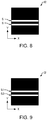
- FIG. 8 is a diagram schematically illustrating a binarized image 12.
- the image I2 includes two blobs, i.e., two slit images S. Accordingly, the arithmetic unit 240 determines that the plurality of slit images S are detected.
- the arithmetic unit 240 specifies, from among the plurality of slit images S, the slit image S1 of the reflected light reflected by the top surface 2a of the specimen 2 based on respective positions of the plurality of slit images on the detection surface 232 of the imaging element 230 (S22).
- the one of the two slit images S over the image I2 having the larger Y-coordinate is determined to be the slit image S 1 of the reflected light reflected by the top surface 2a of the specimen 2.
- the arithmetic unit 240 detects on the image I2 the position of the center (center of gravity) of the slit image S 1 of the reflected light reflected by the top surface 2a of the specimen 2 (S24).
- the arithmetic unit 240 determines the height of the top surface 2a of the specimen 2 based on the position of the slit image S 1 of the reflected light reflected by the top surface 2a of the specimen 2 on the detection surface 232 of the imaging element 230 (S26).
- the height of the top surface 2a of the specimen 2 can be determined by using Expression (2) shown above.
- the displacement amount ⁇ S between the respective positions of the slit images is an amount of displacement of the height of the top surface 2a of the specimen 2 from, e.g., a height of a reference marker provided on the specimen stage 130 to indicate a reference height position. Accordingly, for example, a position of a center (center of gravity) of a slit image of reflected light reflected by a top surface of the reference marker on the detection surface 232 of the imaging element 230 is measured in advance, and coordinates of the center of gravity of the slit image are stored in the storage device of the arithmetic unit 240.
- a distance in the Y-axis direction between the position of the center of the slit image S1 determined in Step S24 and the position of the center of the slit image of the reflected light reflected by the top surface of the reference marker is determined to determine the displacement amount ⁇ S. Then, the determined displacement amount ⁇ S is substituted in Expression (2) to determine a height variation ⁇ H.
- the arithmetic unit 240 detects the position of the center of the slit image (S24) and determines the height of the top surface 2a of the specimen 2 (S26).
- the control unit 300 performs processing such as processing of controlling each of the constituent units of the electro-optical system 100 and processing of controlling the specimen stage 130.
- the control unit 300 includes a processor such as a CPU and a storage device including a RAM, a ROM, and the like. In the storage device, programs for performing various control processing and data are stored. A function of the control unit 300 can be implemented through execution of the programs by the processor.
- a control signal for controlling the objective lens 118 generated by the control unit 300 is converted by a D/A converter 320 to an analog signal, which is supplied to the objective lens 118.
- a control signal for controlling the positioning deflector 120 generated by the control unit 300 is converted by a D/A converter 322 to the analog signal, which is supplied to the positioning deflector 120.
- the electron beam lithography apparatus 1000 combines deflection of the electron beam and movement of the specimen 2 to draw a figure on the top surface 2a of the specimen 2. Specifically, the control unit 300 repeats drawing in a range (field) in which the electron beam is deflected and movement of the specimen 2 to a subsequent field to draw the figure on the top surface 2a of the specimen 2.
- the height measuring device 200 measures the height of the top surface 2a of the specimen 2 and, on each movement between the fields, the control unit 300 acquires information on the height of the top surface 2a of the specimen 2 from the height measuring device 200 and corrects the focus of the objective lens 118 and the deflection angle of the electron beam in the positioning deflector 120.
- the control unit 300 when the control unit 300 operates the specimen stage 130 to move the specimen 2, the height measuring device 200 measures the height of the top surface 2a of the specimen 2. The control unit 300 acquires the information on the height of the top surface 2a of the specimen 2 from the height measuring device 200 and corrects the focus of the objective lens 118 and the deflection angle of the electron beam in the positioning deflector 120. Then, the control unit 300 performs drawing using the electron beam on the top surface 2a of the specimen 2.
- the control unit 300 operates the specimen stage 130 to move the specimen 2, in a similar manner, the height measuring device 200 measures the height of the top surface 2a of the specimen 2, and the control unit 300 corrects the focus of the objective lens 118 and the deflection angle of the electron beam in the positioning deflector 120 and performs drawing.
- the arithmetic unit 240 performs the processing of identifying, from among the plurality of slit images, the slit image of the reflected light reflected by the top surface 2a of the specimen 2 based on the respective positions of the plurality of slit images on the detection surface 232 of the imaging element 230 and the processing of determining the height of the top surface 2a of the specimen 2 based on the position of the slit image of the reflected light reflected by the top surface 2a of the specimen 2 on the detection surface 232.
- the height measuring device 200 when the height of the top surface 2a of the specimen 2 increases as a coordinate (Y-coordinate) in a predetermined direction (Y-axis direction) of each of the slit images increases on the detection surface 232 of the imaging element 230, in the processing of identifying the slit image of the reflected light reflected by the top surface 2a of the specimen 2, the slit image having the largest coordinate (Y-coordinate) in the predetermined direction among the plurality of slit images detected by the imaging element 230 is determined to be the slit image of the reflected light reflected by the top surface 2a of the specimen 2. Consequently, in the height measuring device 200, it is possible to easily identify the slit image of the reflected light reflected by the top surface 2a of the specimen 2 from among the plurality of slit images in the image photographed by the imaging element 230.
- the light source 210 is the light emitting diode. Accordingly, in the height measuring device 200, it is possible to prevent the reflected light emitted from the light source 210 and reflected by the top surface 2a of the specimen 2 and the reflected light reflected by the back surface 2b of the specimen 2 from interfering with each other.
- the light source 210 when the light source 210 is a laser diode, the reflected light reflected by the top surface 2a of the specimen 2 and the reflected light reflected by the back surface 2b of the specimen 2 may interfere with each other. When the reflected light beams interfere with each other, an interference fringe occurs, and the slit images cannot clearly be photographed by the imaging element 230. By contrast, when the light source 210 is the light emitting diode, no interference occurs between the reflected light beams. Consequently, in the height measuring device 200, the slit images can clearly be photographed without being affected by the interference fringe.
- the light source 210 is the light emitting diode, stability is higher than when the light source 210 is a halogen lamp or the like, and accordingly a response is rapid. Consequently, in the height measuring device 200, the light source 210 can be turned ON only when, e.g., the slit images are photographed by the imaging element 230.
- the light source 210 is the halogen lamp having a low response speed or the like
- the height measurement takes time.
- the light source 210 is the light emitting diode having a high response speed, and therefore such a problem does not arise.
- the height measuring method includes the steps of forming a slit image on the top surface 2a of the specimen 2 by using the light source 210 that emits light in a direction oblique to the top surface 2a of the specimen 2 and the slit 222 that shapes the light from the light source 210, detecting the reflected light reflected by the specimen 2 by using the imaging element 230, identifying, when a plurality of the slit images are detected by the imaging element 230, the slit image of the reflected light reflected by the top surface 2a of the specimen 2 from among the plurality of slit images based on respective positions of the plurality of slit images on the detection surface 232 of the imaging element 230, and determining the height of the top surface 2a of the specimen 2 based on the position of the slit image of the reflected light reflected by the top surface 2a of the specimen 2 on the detection surface 232. This allows the height of the top surface 2a of the specimen 2 to be accurately determined.
- the electron beam lithography apparatus 1000 has been described as an example of the charged particle beam apparatus according to the invention.
- the charged particle beam apparatus according to the invention is not limited to the electron beam lithography apparatus 1000, and may also be a scanning electron microscope (SEM), a focused ion beam apparatus (FIB), or the like.
- SEM scanning electron microscope
- FIB focused ion beam apparatus
- the focus of the objective lens can accurately be adjusted based on the height of the top surface of the specimen measured by the height measuring device 200.
- the invention includes configurations that are substantially the same as the configurations described in the embodiments.
- Substantially same configurations means configurations that are the same in function and method, for example.
- the invention also includes configurations in which non-essential elements described in the embodiments are replaced by other elements.
- the invention further includes configurations obtained by adding known art to the configurations described in the embodiments.
Landscapes
- Chemical & Material Sciences (AREA)
- Analytical Chemistry (AREA)
- Physics & Mathematics (AREA)
- General Physics & Mathematics (AREA)
- Length Measuring Devices By Optical Means (AREA)
- Instruments For Measurement Of Length By Optical Means (AREA)
- Exposure And Positioning Against Photoresist Photosensitive Materials (AREA)
- Electron Beam Exposure (AREA)
Abstract
Description
- The present invention relates to a height measuring device, a charged particle beam apparatus, and a height measuring method.
- In an electron beam lithography apparatus, to implement high-accuracy drawing, a height of a top surface of a material is measured before drawing is performed.
- For example,
JP-A-2006-216834 - In the height measuring method disclosed in
JP-A-2006-216834 - When a height of a top surface of a transparent material, which transmits light from a slight source, is measured in the electron beam lithography apparatus as described above, a slit image of the reflected light reflected by the top surface of the material and a slit image of the reflected light reflected by a back surface of the material are detected. In this case, when the two slit images cannot be distinguished from each other and the height of the top surface of the material is determined based on the position of the slit image of the reflected light reflected by the back surface of the material, the height of the top surface of the material cannot accurately be measured.
- According to a first aspect of the invention, there is provided a height measuring device including:
- a light source that emits light in a direction oblique to a top surface of a specimen;
- a slit that shapes the light from the light source to form a slit image on the specimen;
- an imaging element that detects reflected light reflected by the specimen; and
- an arithmetic unit that determines a height of the top surface of the specimen based on a result of detection of the slit image by the imaging element,
- the arithmetic unit performing processing of:
- identifying, when a plurality of slit images are detected by the imaging element, a slit image of the reflected light reflected by the top surface of the specimen from among the plurality of slit images based on respective positions of the plurality of slit images on a detection surface of the imaging element; and
- determining the height of the top surface of the specimen based on the position of the slit image of the reflected light reflected by the top surface of the specimen on the detection surface.
- According to a second aspect of the invention, there is provided a charged particle beam apparatus including the height measuring device described above.
- According to a third aspect of the invention, there is provided a height measuring method including:
- forming a slit image on a top surface of a specimen by using a light source that emits light in a direction oblique to the top surface of the specimen and a slit that shapes the light from the light source;
- detecting reflected light reflected by the specimen by using an imaging element;
- identifying, when a plurality of slit images are detected by the imaging element, a slit image of the reflected light reflected by the top surface of the specimen from among the plurality of slit images based on respective positions of the plurality of slit images on a detection surface of the imaging element; and
- determining a height of the top surface of the specimen based on the position of the slit image of the reflected light reflected by the top surface of the specimen on the detection surface.
-
-
FIG. 1 is a diagram illustrating a configuration of an electron beam lithography apparatus according to an embodiment of the invention. -
FIG. 2 is a diagram schematically illustrating a configuration of a height measuring device. -
FIG. 3 is a diagram for explaining a principle of height measurement. -
FIG. 4 is a diagram for explaining a technique of measuring a displacement amount ΔS. -
FIG. 5 is a diagram for explaining a technique of identifying, when a specimen is made of a transparent material, a slit image of reflected light reflected by a top surface of the specimen. -
FIG. 6 is a diagram for explaining, when the specimen is made of the transparent material, a technique of identifying a slit image of reflected light reflected by a top surface of the specimen. -
FIG. 7 is a flow chart illustrating an example of processing in an arithmetic unit. -
FIG. 8 is a diagram schematically illustrating a binarized image. -
FIG. 9 is a diagram schematically illustrating a binarized image. - A height measuring device according to an embodiment of the invention includes:
- a light source that emits light in a direction oblique to a top surface of a specimen;
- a slit that shapes the light from the light source to form a slit image on the specimen;
- an imaging element that detects reflected light reflected by the specimen; and
- an arithmetic unit that determines a height of the top surface of the specimen based on a result of detection of the slit image by the imaging element,
- the arithmetic unit performing processing of:
- identifying, when a plurality of slit images are detected by the imaging element, a slit image of the reflected light reflected by the top surface of the specimen from among the plurality of slit images based on respective positions of the plurality of slit images on a detection surface of the imaging element; and
- determining the height of the top surface of the specimen based on the position of the slit image of the reflected light reflected by the top surface of the specimen on the detection surface.
- In such a height measuring device, when a plurality of slit images are detected by an imaging element, the slit image of reflected light reflected by a top surface of a specimen can be identified. This prevents a height of the top surface of the specimen from being determined based on a slit image of the reflected light reflected by a back surface of the specimen and allows the height of the top surface of the specimen to be accurately measured.
- A charged particle beam apparatus according to an embodiment of the invention includes the height measuring device described above.
- Such a charged particle beam apparatus allows a height of a top surface of a specimen to be accurately measured.
- A height measuring method according to an embodiment of the invention includes:
- forming a slit image on a top surface of a specimen by using a light source that emits light in a direction oblique to the top surface of the specimen and a slit that shapes the light from the light source;
- detecting reflected light reflected by the specimen by using an imaging element;
- identifying, when a plurality of slit images are detected by the imaging element, a slit image of the reflected light reflected by the top surface of the specimen from among the plurality of slit images based on respective positions of the plurality of slit images on a detection surface of the imaging element; and
- determining a height of the top surface of the specimen based on the position of the slit image of the reflected light reflected by the top surface of the specimen on the detection surface.
- In such a height measuring method, when a plurality of slit images are detected by an imaging element, the slit image of reflected light reflected by a top surface of a specimen can be identified. This prevents a height of the top surface of the specimen from being determined based on a slit image of the reflected light reflected by a back surface of the specimen and allows the height of the top surface of the specimen to be accurately measured.
- Preferred embodiments of the invention are described in detail below with reference to the drawings. It is noted that the following embodiments do not unduly limit the scope of the invention as stated in the claims. In addition, all of the elements described below are not necessarily essential requirements of the invention.
- The following will describe an electron beam lithography apparatus as an example of the charged particle beam apparatus according to the invention, but the charged particle beam apparatus according to the invention is not limited to the electron beam lithography apparatus.
- With reference to the drawings, a description will be given first of an electron beam lithography apparatus according to an embodiment of the invention.
FIG. 1 is a diagram illustrating a configuration of an electronbeam lithography apparatus 1000 according to the present embodiment. - The electron
beam lithography apparatus 1000 is an apparatus which irradiates aspecimen 2 with an electron beam to draw a pattern on thespecimen 2. The electronbeam lithography apparatus 1000 is an apparatus which draws an extremely fine pattern, such as a semiconductor integrated circuit pattern, on a substrate such as, e.g., a semiconductor substrate or a mask blank. Thespecimen 2 mentioned herein is, e.g., a substrate such as a semiconductor substrate or a mask blank. - The electron
beam lithography apparatus 1000 includes an electro-optical system 100, aheight measuring device 200, and acontrol unit 300. - The electro-
optical system 100 includes anelectron gun 102, a blanker 104, anirradiation lens 106, afirst slit 108, a shapingdeflector 110, a shapinglens 112, asecond slit 114, areduction lens 116, anobjective lens 118, and apositioning deflector 120. - The
electron gun 102 generates an electron beam. The blanker 104 deflects the electron beam emitted from theelectron gun 102 to adjust a time required by the electron beam to pass through thefirst slit 108. In other words, it is possible to adjust an amount of the electron beam applied to thespecimen 2 by using theblanker 104. The electron beam having passed through the blanker 104 is applied to thefirst slit 108 via theirradiation lens 106. - The
first slit 108, the shapingdeflector 110, the shapinglens 112, and thesecond slit 114 shape the electron beam. An image formed by the passage of the electron beam through thefirst slit 108 is formed over thesecond slit 114 by the shapinglens 112. At this time, by deflecting the electron beam with the shapingdeflector 110, it is possible to change a position of the image formed by thefirst slit 108 over thesecond slit 114. Thus, the electron beam can be shaped. By controlling a direction in which the electron beam is deflected and an amount of the deflection of the electron beam in the shapingdeflector 110, the electron beam can be shaped into any shape. - The
reduction lens 116 reduces the image formed by thefirst slit 108, the shapingdeflector 110, the shapinglens 112, and thesecond slit 114. Theobjective lens 118 forms the image reduced by thereduction lens 116 onto thespecimen 2. Thepositioning deflector 120 deflects the electron beam having passed through theobjective lens 118. Thus, it is possible to change a position of the electron beam irradiating thespecimen 2. In other words, thepositioning deflector 120 can determine the position of the image formed by thefirst slit 108 and the like on thespecimen 2. - The electron
beam lithography apparatus 1000 has aspecimen stage 130 for supporting thespecimen 2. Thespecimen stage 130 includes a moving mechanism for moving thespecimen 2. - The electron
beam lithography apparatus 1000 can shape the electron beam by using thefirst slit 108, the shapingdeflector 110, the shapinglens 112, and thesecond slit 114 and control a cross-sectional shape of the electron beam to be applied to thespecimen 2, i.e., a shot shape and a shot size. The electronbeam lithography apparatus 1000 can also control a time during which the electron beam irradiates thespecimen 2, i.e., a shot time by using theblanker 104. In addition, the electronbeam lithography apparatus 1000 can control a position of the electron beam irradiating thespecimen 2, i.e., a shot position, by using thepositioning deflector 120. -
FIG. 2 is a diagram schematically illustrating a configuration of aheight measuring device 200. - As illustrated in
FIGS. 1 and2 , theheight measuring device 200 includes alight source 210, aslit member 220 provided with aslit 222, animaging element 230, and anarithmetic unit 240. - The
light source 210 emits light in a direction oblique to atop surface 2a of thespecimen 2. Thelight source 210 illuminates theslit member 220. Thelight source 210 is a light emitting diode (LED). For example, thelight source 210 is an infrared light emitting diode. For example, thelight source 210 is the light emitting diode having a wavelength range of not less than 850 nm and not more than 950 nm and a peak wavelength of 870 nm. - In the
slit member 220, theslit 222 is formed to allow the light from thelight source 210 to pass therethrough. The light having passed through theslit 222 irradiates thetop surface 2a of thespecimen 2. As a result, a slit image is formed on thetop surface 2a of thespecimen 2. Note that, between theslit member 220 and thespecimen 2, a lens included in an illumination optical system may also be disposed, though not shown. The illumination optical system allows the slit image formed by theslit 222 to be formed on thetop surface 2a of thespecimen 2. - The
imaging element 230 detects the reflected light reflected by thespecimen 2. For example, theimaging element 230 is a digital camera such as a charge coupled device (CCD) camera or a complementary metal oxide semiconductor (CMOS) camera. Note that, between thespecimen 2 and theimaging element 230, an image forming optical system may also be disposed, though not shown. The image forming optical system allows the slit image on thespecimen 2 to be formed on adetection surface 232 of theimaging element 230. - The
imaging element 230 can obtain an image including the slit image as a result of the detection of the slit image. In an image photographed by theimaging element 230, a brightness of the slit image is higher than that of the other portion. - The
arithmetic unit 240 performs processing of determining a height of thetop surface 2a of thespecimen 2 based on the result of the detection of the slit image by theimaging element 230. For example, thearithmetic unit 240 includes a processor such as a central processing unit (CPU) and a storage device including a random access memory (RAM), a read only memory (ROM), and the like. In the storage device, programs for performing various calculation processing and data are stored. A function of thearithmetic unit 240 can be implemented through execution of the programs by the processor. -
FIG. 3 is a diagram for explaining a principle of height measurement. - As illustrated in
FIG. 3 , it is assumed that θ represents an incidence angle of an optical axis L1 of the light incident on the top surface of the specimen. When the top surface of the specimen is at a position A, an optical axis of the light regularly reflected by the top surface of the specimen corresponds to an optical axis L2 illustrated inFIG. 3 . When the top surface of the specimen is at a position B, the optical axis of the light regularly reflected by the top surface of the specimen corresponds to an optical axis L4 illustrated inFIG. 3 . When the top surface of the specimen is at the position A, aslit image S 1 on the top surface of the specimen is enlarged by the image forming optical system to be formed on the detection surface of the imaging element. When the top surface of the specimen is at the position B, a slit image S2 is enlarged by the image forming optical system to be formed on the detection surface of the imaging element. The slit image S2 is a mirror image of the slit image S1 with respect to the top surface of the specimen. - When it is assumed that a height variation from the position A to the position B is ΔH and a magnification of the image forming optical system is M, a displacement amount ΔS between respective positions of the slit images on the detection surface of the imaging element is given by Expression (1) shown below.

- Accordingly, the height variation ΔH of the top surface of the specimen is given by Expression (2) shown below.

- Accordingly, by measuring the displacement amount ΔS between the respective positions of the slit images on the detection surface of the imaging element, it is possible to determine the height variation ΔH of the top surface of the specimen by using Expression (2) shown above.
-
FIG. 4 is a diagram for explaining a method of measuring the displacement amount ΔS. - As illustrated in
FIG. 4 , it is possible to measure the displacement amount ΔS between the position of the slit image S1 and the position of the slit image S2 on thedetection surface 232 of theimaging element 230. In the illustrated example, on thedetection surface 232 of theimaging element 230, a Y-axis direction corresponds to a height direction of thetop surface 2a of thespecimen 2, while an X-axis direction corresponds to a width direction of each of the slit images. Accordingly, by measuring, e.g., a distance in the Y-axis direction between a position of a center (center of gravity) of theslit image S 1 and a position of a center (center of gravity) of the slit image S2, it is possible to measure the displacement amount ΔS. - As described above, on the
detection surface 232 of theimaging element 230, the Y-axis direction corresponds to the height of thetop surface 2a of thespecimen 2. Specifically, on thedetection surface 232, as a Y-coordinate is larger, the height of thetop surface 2a of thespecimen 2 is larger. Since a Y-coordinate of the center of the slit image S1 is larger than a Y-coordinate of the center of the slit image S2, thetop surface 2a of thespecimen 2 when theslit image S 1 is detected is higher than thetop surface 2a of thespecimen 2 when the slit image S2 is detected. -
FIGS. 5 and 6 are diagrams for explaining a technique of identifying, when thespecimen 2 is made of a transparent material, a slit image of the reflected light reflected by thetop surface 2a of thespecimen 2. - As illustrated in
FIG. 5 , when thespecimen 2 is made of a transparent material that transmits the light emitted from thelight source 210, such as a glass substrate, the light from thelight source 210 is reflected by thetop surface 2a of thespecimen 2, while being transmitted by thespecimen 2 to be reflected also by aback surface 2b of thespecimen 2. Consequently, in theimaging element 230, theslit image S 1 of the reflected light reflected by thetop surface 2a of thespecimen 2 and a slit image S3 of the reflected light reflected by theback surface 2b of thespecimen 2 are detected. As a result, it is required to identify which one of the two slit images (theslit image S 1 and the slit image S3) is theslit image S 1 of the reflected light reflected by thetop surface 2a of thespecimen 2. - As illustrated in
FIG. 5 , the optical axis of the reflected light reflected by thetop surface 2a of thespecimen 2 corresponds to the optical axis L2, and an optical axis of the reflected light reflected by thetop surface 2a of thespecimen 2 corresponds to an optical axis L6. As illustrated inFIGS. 5 and 6 , on thedetection surface 232 of theimaging element 230, theslit image S 1 of the reflected light reflected by thetop surface 2a of thespecimen 2 is constantly located in a positive Y-axis direction with respect to the slit image S3 of the reflected light reflected by theback surface 2b of thespecimen 2. In other words, the Y-coordinate of the center of the slit image S1 is larger than a Y-coordinate of a center of the slit image S3. Consequently, when the two slit images are detected by theimaging element 230, the one of the two slit images having the larger Y-coordinate is theslit image S 1 of the reflected light reflected by thetop surface 2a of thespecimen 2. -
FIG. 7 is a flow chart illustrating an example of processing in thearithmetic unit 240. - The
arithmetic unit 240 acquires an image photographed by the imaging element 230 (S10). Then, thearithmetic unit 240 sets a threshold for binarization processing (S 12). The threshold is set to a value which allows the slit image S1 and the slit image S3 to be separated from each other. In the processing of setting the threshold, it may be possible to, e.g., set the threshold to a preset value or set the threshold by using a known threshold determination method. - Then, the
arithmetic unit 240 performs the binarization processing on the acquired image based on the set threshold (S14). Note that, after the binarization processing, thearithmetic unit 240 may also perform filter processing for accentuating the image after subjected to the binarization processing. - Next, the
arithmetic unit 240 detects blobs in the image after subjected to the binarization processing (S16) and extracts, as the slit images, the blobs each occupying an area equal to or larger than a predetermined area set in advance (S18). Thus, it is possible to detect the slit images. - Then, the
arithmetic unit 240 determines whether or not the plurality of slit images are detected (S20). -
FIG. 8 is a diagram schematically illustrating abinarized image 12. As illustrated inFIG. 8 , the image I2 includes two blobs, i.e., two slit images S. Accordingly, thearithmetic unit 240 determines that the plurality of slit images S are detected. - When determining that the plurality of slit images are detected (Yes in S20), the
arithmetic unit 240 specifies, from among the plurality of slit images S, the slit image S1 of the reflected light reflected by thetop surface 2a of thespecimen 2 based on respective positions of the plurality of slit images on thedetection surface 232 of the imaging element 230 (S22). - Specifically, as illustrated in
FIG. 9 , the one of the two slit images S over the image I2 having the larger Y-coordinate is determined to be theslit image S 1 of the reflected light reflected by thetop surface 2a of thespecimen 2. - Then, the
arithmetic unit 240 detects on the image I2 the position of the center (center of gravity) of theslit image S 1 of the reflected light reflected by thetop surface 2a of the specimen 2 (S24). - Then, the
arithmetic unit 240 determines the height of thetop surface 2a of thespecimen 2 based on the position of theslit image S 1 of the reflected light reflected by thetop surface 2a of thespecimen 2 on thedetection surface 232 of the imaging element 230 (S26). The height of thetop surface 2a of thespecimen 2 can be determined by using Expression (2) shown above. - It is assumed that the displacement amount ΔS between the respective positions of the slit images is an amount of displacement of the height of the
top surface 2a of thespecimen 2 from, e.g., a height of a reference marker provided on thespecimen stage 130 to indicate a reference height position. Accordingly, for example, a position of a center (center of gravity) of a slit image of reflected light reflected by a top surface of the reference marker on thedetection surface 232 of theimaging element 230 is measured in advance, and coordinates of the center of gravity of the slit image are stored in the storage device of thearithmetic unit 240. - In processing of determining the height of the
top surface 2a of thespecimen 2, a distance in the Y-axis direction between the position of the center of the slit image S1 determined in Step S24 and the position of the center of the slit image of the reflected light reflected by the top surface of the reference marker is determined to determine the displacement amount ΔS. Then, the determined displacement amount ΔS is substituted in Expression (2) to determine a height variation ΔH. - When determining that the plurality of slit images are not detected, i.e., only one slit image is detected (No in S20), the
arithmetic unit 240 detects the position of the center of the slit image (S24) and determines the height of thetop surface 2a of the specimen 2 (S26). - Through the foregoing processing, it is possible to determine the height of the
top surface 2a of thespecimen 2. - The
control unit 300 performs processing such as processing of controlling each of the constituent units of the electro-optical system 100 and processing of controlling thespecimen stage 130. For example, thecontrol unit 300 includes a processor such as a CPU and a storage device including a RAM, a ROM, and the like. In the storage device, programs for performing various control processing and data are stored. A function of thecontrol unit 300 can be implemented through execution of the programs by the processor. - A control signal for controlling the
objective lens 118 generated by thecontrol unit 300 is converted by a D/A converter 320 to an analog signal, which is supplied to theobjective lens 118. A control signal for controlling thepositioning deflector 120 generated by thecontrol unit 300 is converted by a D/A converter 322 to the analog signal, which is supplied to thepositioning deflector 120. - The electron
beam lithography apparatus 1000 combines deflection of the electron beam and movement of thespecimen 2 to draw a figure on thetop surface 2a of thespecimen 2. Specifically, thecontrol unit 300 repeats drawing in a range (field) in which the electron beam is deflected and movement of thespecimen 2 to a subsequent field to draw the figure on thetop surface 2a of thespecimen 2. - When the height of the
top surface 2a of thespecimen 2 varies, to precisely draw the figure, it is required to measure the height of thetop surface 2a of thespecimen 2 on each movement between the fields and adjust a focus of theobjective lens 118 and a deflection angle of the electron beam in thepositioning deflector 120 based on a variation in the height of thetop surface 2a of thespecimen 2. - Accordingly, in the electron
beam lithography apparatus 1000, on each movement between the fields, theheight measuring device 200 measures the height of thetop surface 2a of thespecimen 2 and, on each movement between the fields, thecontrol unit 300 acquires information on the height of thetop surface 2a of thespecimen 2 from theheight measuring device 200 and corrects the focus of theobjective lens 118 and the deflection angle of the electron beam in thepositioning deflector 120. - Specifically, when the
control unit 300 operates thespecimen stage 130 to move thespecimen 2, theheight measuring device 200 measures the height of thetop surface 2a of thespecimen 2. Thecontrol unit 300 acquires the information on the height of thetop surface 2a of thespecimen 2 from theheight measuring device 200 and corrects the focus of theobjective lens 118 and the deflection angle of the electron beam in thepositioning deflector 120. Then, thecontrol unit 300 performs drawing using the electron beam on thetop surface 2a of thespecimen 2. - Subsequently, when the
control unit 300 operates thespecimen stage 130 to move thespecimen 2, in a similar manner, theheight measuring device 200 measures the height of thetop surface 2a of thespecimen 2, and thecontrol unit 300 corrects the focus of theobjective lens 118 and the deflection angle of the electron beam in thepositioning deflector 120 and performs drawing. - In the electron
beam lithography apparatus 1000, through the repetition of the processing described above by thecontrol unit 300 and theheight measuring device 200, a pattern is drawn on thetop surface 2a of thespecimen 2. - In the
height measuring device 200, when the plurality of slit images are detected by theimaging element 230, thearithmetic unit 240 performs the processing of identifying, from among the plurality of slit images, the slit image of the reflected light reflected by thetop surface 2a of thespecimen 2 based on the respective positions of the plurality of slit images on thedetection surface 232 of theimaging element 230 and the processing of determining the height of thetop surface 2a of thespecimen 2 based on the position of the slit image of the reflected light reflected by thetop surface 2a of thespecimen 2 on thedetection surface 232. Thus, in theheight measuring device 200, it is possible to identify the slit image of the reflected light reflected by thetop surface 2a of thespecimen 2. This prevents the height from being determined based on the slit image of the light reflected by theback surface 2b of thespecimen 2 and allows the height of thetop surface 2a of thespecimen 2 to be accurately measured. - In the
height measuring device 200, when the height of thetop surface 2a of thespecimen 2 increases as a coordinate (Y-coordinate) in a predetermined direction (Y-axis direction) of each of the slit images increases on thedetection surface 232 of theimaging element 230, in the processing of identifying the slit image of the reflected light reflected by thetop surface 2a of thespecimen 2, the slit image having the largest coordinate (Y-coordinate) in the predetermined direction among the plurality of slit images detected by theimaging element 230 is determined to be the slit image of the reflected light reflected by thetop surface 2a of thespecimen 2. Consequently, in theheight measuring device 200, it is possible to easily identify the slit image of the reflected light reflected by thetop surface 2a of thespecimen 2 from among the plurality of slit images in the image photographed by theimaging element 230. - In the
height measuring device 200, thelight source 210 is the light emitting diode. Accordingly, in theheight measuring device 200, it is possible to prevent the reflected light emitted from thelight source 210 and reflected by thetop surface 2a of thespecimen 2 and the reflected light reflected by theback surface 2b of thespecimen 2 from interfering with each other. - For example, when the
light source 210 is a laser diode, the reflected light reflected by thetop surface 2a of thespecimen 2 and the reflected light reflected by theback surface 2b of thespecimen 2 may interfere with each other. When the reflected light beams interfere with each other, an interference fringe occurs, and the slit images cannot clearly be photographed by theimaging element 230. By contrast, when thelight source 210 is the light emitting diode, no interference occurs between the reflected light beams. Consequently, in theheight measuring device 200, the slit images can clearly be photographed without being affected by the interference fringe. - In addition, in the
height measuring device 200, since thelight source 210 is the light emitting diode, stability is higher than when thelight source 210 is a halogen lamp or the like, and accordingly a response is rapid. Consequently, in theheight measuring device 200, thelight source 210 can be turned ON only when, e.g., the slit images are photographed by theimaging element 230. - For example, in a case where the
light source 210 is the halogen lamp having a low response speed or the like, when thelight source 210 is turned ON/OFF every time height measurement is performed, the height measurement takes time. Meanwhile, in a state where thelight source 210 is constantly ON, when a specimen image is observed using a reflected electron detector or the like in the electronbeam lithography apparatus 1000, there is a risk that the reflected electron detector may detect the light from thelight source 210. By contrast, in theheight measuring device 200, thelight source 210 is the light emitting diode having a high response speed, and therefore such a problem does not arise. - The height measuring method according to the present embodiment includes the steps of forming a slit image on the
top surface 2a of thespecimen 2 by using thelight source 210 that emits light in a direction oblique to thetop surface 2a of thespecimen 2 and theslit 222 that shapes the light from thelight source 210, detecting the reflected light reflected by thespecimen 2 by using theimaging element 230, identifying, when a plurality of the slit images are detected by theimaging element 230, the slit image of the reflected light reflected by thetop surface 2a of thespecimen 2 from among the plurality of slit images based on respective positions of the plurality of slit images on thedetection surface 232 of theimaging element 230, and determining the height of thetop surface 2a of thespecimen 2 based on the position of the slit image of the reflected light reflected by thetop surface 2a of thespecimen 2 on thedetection surface 232. This allows the height of thetop surface 2a of thespecimen 2 to be accurately determined. - Note that the invention is not limited to the embodiments described above, and can variously be modified within the scope of the invention.
- In the embodiments described above, the electron
beam lithography apparatus 1000 has been described as an example of the charged particle beam apparatus according to the invention. However, the charged particle beam apparatus according to the invention is not limited to the electronbeam lithography apparatus 1000, and may also be a scanning electron microscope (SEM), a focused ion beam apparatus (FIB), or the like. For example, in the scanning electron microscope including theheight measuring device 200, the focus of the objective lens can accurately be adjusted based on the height of the top surface of the specimen measured by theheight measuring device 200. - The invention is not limited to the above-described embodiments, and various modifications can be made. For example, the invention includes configurations that are substantially the same as the configurations described in the embodiments. Substantially same configurations means configurations that are the same in function and method, for example. The invention also includes configurations in which non-essential elements described in the embodiments are replaced by other elements. The invention further includes configurations obtained by adding known art to the configurations described in the embodiments.
- Some embodiments of the invention have been described in detail above, but a person skilled in the art will readily appreciate that various modifications can be made from the embodiments without materially departing from the novel teachings and effects of the invention as defined by the appended claims. Accordingly, all such modifications are assumed to be included in the scope of the invention.
Claims (5)
- A height measuring device comprising:a light source that emits light in a direction oblique to a top surface of a specimen;a slit that shapes the light from the light source to form a slit image on the specimen;an imaging element that detects reflected light reflected by the specimen; andan arithmetic unit that determines a height of the top surface of the specimen based on a result of detection of the slit image by the imaging element,the arithmetic unit performing processing of:identifying, when a plurality of slit images are detected by the imaging element, a slit image of the reflected light reflected by the top surface of the specimen from among the plurality of slit images based on respective positions of the plurality of slit images on a detection surface of the imaging element; anddetermining the height of the top surface of the specimen based on the position of the slit image of the reflected light reflected by the top surface of the specimen on the detection surface.
- The height measuring device according to claim 1, wherein
when the height of the top surface of the specimen increases as a coordinate of the slit image in a predetermined direction increases on the detection surface,
in the processing of identifying the slit image of the reflected light reflected by the top surface of the specimen,
a slit image having the largest coordinate in the predetermined direction from among the plurality of slit images detected by the imaging element is identified to be the slit image of the reflected light reflected by the top surface of the specimen. - The height measuring device according to claim 1 or 2, wherein the light source is a light emitting diode.
- A charged particle beam apparatus comprising the height measuring device according to any one of claims 1 to 3.
- A height measuring method comprising:forming a slit image on a top surface of a specimen by using a light source that emits light in a direction oblique to the top surface of the specimen and a slit that shapes the light from the light source;detecting reflected light reflected by the specimen by using an imaging element;identifying, when a plurality of slit images are detected by the imaging element, a slit image of the reflected light reflected by the top surface of the specimen from among the plurality of slit images based on respective positions of the plurality of slit images on a detection surface of the imaging element; anddetermining a height of the top surface of the specimen based on the position of the slit image of the reflected light reflected by the top surface of the specimen on the detection surface.
Applications Claiming Priority (1)
| Application Number | Priority Date | Filing Date | Title |
|---|---|---|---|
| JP2020000798A JP7083856B2 (en) | 2020-01-07 | 2020-01-07 | Height measuring device, charged particle beam device, and height measuring method |
Publications (2)
| Publication Number | Publication Date |
|---|---|
| EP3848669A1 true EP3848669A1 (en) | 2021-07-14 |
| EP3848669B1 EP3848669B1 (en) | 2024-06-19 |
Family
ID=73834310
Family Applications (1)
| Application Number | Title | Priority Date | Filing Date |
|---|---|---|---|
| EP20213469.8A Active EP3848669B1 (en) | 2020-01-07 | 2020-12-11 | Height measuring device, charged particle beam apparatus, and height measuring method |
Country Status (3)
| Country | Link |
|---|---|
| US (1) | US11754388B2 (en) |
| EP (1) | EP3848669B1 (en) |
| JP (1) | JP7083856B2 (en) |
Families Citing this family (2)
| Publication number | Priority date | Publication date | Assignee | Title |
|---|---|---|---|---|
| US12451324B2 (en) * | 2020-03-13 | 2025-10-21 | Asml Netherlands B.V. | Leveling sensor in multiple charged-particle beam inspection |
| US20250087450A1 (en) * | 2023-09-13 | 2025-03-13 | Kla Corporation | Optics for In-Situ Scanning Electron Microscope Repair |
Citations (4)
| Publication number | Priority date | Publication date | Assignee | Title |
|---|---|---|---|---|
| JP2006216834A (en) | 2005-02-04 | 2006-08-17 | Jeol Ltd | Method for measuring height in electron beam lithography system |
| EP1750087A1 (en) * | 2004-06-04 | 2007-02-07 | Asahi Glass Company, Limited | Method and apparatus for inspecting front surface shape |
| CN102713583A (en) * | 2010-11-25 | 2012-10-03 | 塞米西斯科株式会社 | System and method for measuring irregularity of glass substrate |
| KR20160002104A (en) * | 2014-06-30 | 2016-01-07 | 삼성전자주식회사 | Thickness measuring apparatus and control method for the same |
Family Cites Families (12)
| Publication number | Priority date | Publication date | Assignee | Title |
|---|---|---|---|---|
| US5654903A (en) * | 1995-11-07 | 1997-08-05 | Lucent Technologies Inc. | Method and apparatus for real time monitoring of wafer attributes in a plasma etch process |
| US6104486A (en) * | 1995-12-28 | 2000-08-15 | Fujitsu Limited | Fabrication process of a semiconductor device using ellipsometry |
| US6031615A (en) * | 1997-09-22 | 2000-02-29 | Candela Instruments | System and method for simultaneously measuring lubricant thickness and degradation, thin film thickness and wear, and surface roughness |
| US6483580B1 (en) * | 1998-03-06 | 2002-11-19 | Kla-Tencor Technologies Corporation | Spectroscopic scatterometer system |
| US6271047B1 (en) * | 1998-05-21 | 2001-08-07 | Nikon Corporation | Layer-thickness detection methods and apparatus for wafers and the like, and polishing apparatus comprising same |
| JP2005265841A (en) * | 2004-02-17 | 2005-09-29 | Omron Corp | Optical measuring apparatus and optical measuring method |
| JP4426519B2 (en) * | 2005-11-11 | 2010-03-03 | 株式会社日立ハイテクノロジーズ | Optical height detection method, electron beam measuring device, and electron beam inspection device |
| JP2012215399A (en) * | 2011-03-31 | 2012-11-08 | Panasonic Industrial Devices Sunx Co Ltd | Displacement sensor system and displacement sensor |
| CN104220932B (en) * | 2012-02-21 | 2017-02-22 | Asml荷兰有限公司 | Inspection apparatus and method |
| JP2013228264A (en) * | 2012-04-25 | 2013-11-07 | Toray Eng Co Ltd | Protrusion height measuring apparatus |
| JP2017083234A (en) * | 2015-10-26 | 2017-05-18 | オムロン株式会社 | Three-dimensional shape measurement device, three-dimensional shape measurement system, program, computer-readable recording medium, and three-dimensional shape measurement method |
| DE102017204861A1 (en) * | 2017-03-23 | 2018-09-27 | Carl Zeiss Smt Gmbh | Method for determining a material removal and apparatus for the beam processing of a workpiece |
-
2020
- 2020-01-07 JP JP2020000798A patent/JP7083856B2/en active Active
- 2020-12-11 EP EP20213469.8A patent/EP3848669B1/en active Active
-
2021
- 2021-01-04 US US17/140,302 patent/US11754388B2/en active Active
Patent Citations (4)
| Publication number | Priority date | Publication date | Assignee | Title |
|---|---|---|---|---|
| EP1750087A1 (en) * | 2004-06-04 | 2007-02-07 | Asahi Glass Company, Limited | Method and apparatus for inspecting front surface shape |
| JP2006216834A (en) | 2005-02-04 | 2006-08-17 | Jeol Ltd | Method for measuring height in electron beam lithography system |
| CN102713583A (en) * | 2010-11-25 | 2012-10-03 | 塞米西斯科株式会社 | System and method for measuring irregularity of glass substrate |
| KR20160002104A (en) * | 2014-06-30 | 2016-01-07 | 삼성전자주식회사 | Thickness measuring apparatus and control method for the same |
Also Published As
| Publication number | Publication date |
|---|---|
| US20210207945A1 (en) | 2021-07-08 |
| US11754388B2 (en) | 2023-09-12 |
| EP3848669B1 (en) | 2024-06-19 |
| JP2021110566A (en) | 2021-08-02 |
| JP7083856B2 (en) | 2022-06-13 |
Similar Documents
| Publication | Publication Date | Title |
|---|---|---|
| US7692144B2 (en) | Electron beam exposure or system inspection or measurement apparatus and its method and height detection apparatus | |
| US8487250B2 (en) | Method for detecting information of an electronic potential on a sample and charged particle beam apparatus | |
| TWI494537B (en) | A pattern measuring method, a device condition setting method of a charged particle beam device, and a charged particle beam device | |
| US20080290274A1 (en) | Defect review method and device for semiconductor device | |
| US9213001B2 (en) | Focal position adjustment method and inspection method | |
| JP6431786B2 (en) | Line width error acquisition method, line width error acquisition apparatus, and inspection system | |
| US20180337019A1 (en) | Scanning Transmission Electron Microscope and Method of Image Generation | |
| JP6666627B2 (en) | Charged particle beam device and method of adjusting charged particle beam device | |
| US11276552B2 (en) | Method for image adjustment and charged particle beam system | |
| US11754388B2 (en) | Height measuring device, charged particle beam apparatus, and height measuring method | |
| US7767982B2 (en) | Optical auto focusing system and method for electron beam inspection tool | |
| JP2016033461A (en) | Height measuring device | |
| JP2001202912A (en) | Alignment method of aperture and optical axis of charged particle beam device | |
| CN111693553B (en) | Method and system for ribbon axis alignment | |
| US20200279715A1 (en) | Optical height detection system | |
| JP6909859B2 (en) | Charged particle beam device | |
| US11545337B2 (en) | Scanning transmission electron microscope and adjustment method of optical system | |
| WO2010146927A1 (en) | Pattern inspection device and pattern inspection method | |
| US6414325B1 (en) | Charged particle beam exposure apparatus and exposure method capable of highly accurate exposure in the presence of partial unevenness on the surface of exposed specimen | |
| JP5372445B2 (en) | Scanning electron microscope apparatus and focusing method thereof | |
| KR101928394B1 (en) | Method of measuring resolution of charged particle beam and charged particle beam writing apparatus | |
| US20230071801A1 (en) | Electron beam application apparatus and inspection method | |
| JP7841012B2 (en) | Transmission electron microscope, image classification method, and electron beam adjustment method | |
| JP4146951B2 (en) | Beam irradiation apparatus and electron beam exposure apparatus | |
| US12191111B2 (en) | Charged particle beam system and method for determining observation conditions in charged particle beam device |
Legal Events
| Date | Code | Title | Description |
|---|---|---|---|
| PUAI | Public reference made under article 153(3) epc to a published international application that has entered the european phase |
Free format text: ORIGINAL CODE: 0009012 |
|
| STAA | Information on the status of an ep patent application or granted ep patent |
Free format text: STATUS: THE APPLICATION HAS BEEN PUBLISHED |
|
| AK | Designated contracting states |
Kind code of ref document: A1 Designated state(s): AL AT BE BG CH CY CZ DE DK EE ES FI FR GB GR HR HU IE IS IT LI LT LU LV MC MK MT NL NO PL PT RO RS SE SI SK SM TR |
|
| STAA | Information on the status of an ep patent application or granted ep patent |
Free format text: STATUS: REQUEST FOR EXAMINATION WAS MADE |
|
| 17P | Request for examination filed |
Effective date: 20210927 |
|
| RBV | Designated contracting states (corrected) |
Designated state(s): AL AT BE BG CH CY CZ DE DK EE ES FI FR GB GR HR HU IE IS IT LI LT LU LV MC MK MT NL NO PL PT RO RS SE SI SK SM TR |
|
| STAA | Information on the status of an ep patent application or granted ep patent |
Free format text: STATUS: EXAMINATION IS IN PROGRESS |
|
| 17Q | First examination report despatched |
Effective date: 20230524 |
|
| GRAP | Despatch of communication of intention to grant a patent |
Free format text: ORIGINAL CODE: EPIDOSNIGR1 |
|
| STAA | Information on the status of an ep patent application or granted ep patent |
Free format text: STATUS: GRANT OF PATENT IS INTENDED |
|
| RIC1 | Information provided on ipc code assigned before grant |
Ipc: H01J 37/20 20060101ALI20231222BHEP Ipc: G01B 11/06 20060101AFI20231222BHEP |
|
| INTG | Intention to grant announced |
Effective date: 20240119 |
|
| GRAS | Grant fee paid |
Free format text: ORIGINAL CODE: EPIDOSNIGR3 |
|
| GRAA | (expected) grant |
Free format text: ORIGINAL CODE: 0009210 |
|
| STAA | Information on the status of an ep patent application or granted ep patent |
Free format text: STATUS: THE PATENT HAS BEEN GRANTED |
|
| AK | Designated contracting states |
Kind code of ref document: B1 Designated state(s): AL AT BE BG CH CY CZ DE DK EE ES FI FR GB GR HR HU IE IS IT LI LT LU LV MC MK MT NL NO PL PT RO RS SE SI SK SM TR |
|
| RAP3 | Party data changed (applicant data changed or rights of an application transferred) |
Owner name: JEOL LTD. |
|
| REG | Reference to a national code |
Ref country code: GB Ref legal event code: FG4D |
|
| REG | Reference to a national code |
Ref country code: CH Ref legal event code: EP |
|
| REG | Reference to a national code |
Ref country code: DE Ref legal event code: R096 Ref document number: 602020032574 Country of ref document: DE |
|
| PG25 | Lapsed in a contracting state [announced via postgrant information from national office to epo] |
Ref country code: BG Free format text: LAPSE BECAUSE OF FAILURE TO SUBMIT A TRANSLATION OF THE DESCRIPTION OR TO PAY THE FEE WITHIN THE PRESCRIBED TIME-LIMIT Effective date: 20240619 |
|
| PG25 | Lapsed in a contracting state [announced via postgrant information from national office to epo] |
Ref country code: FI Free format text: LAPSE BECAUSE OF FAILURE TO SUBMIT A TRANSLATION OF THE DESCRIPTION OR TO PAY THE FEE WITHIN THE PRESCRIBED TIME-LIMIT Effective date: 20240619 Ref country code: HR Free format text: LAPSE BECAUSE OF FAILURE TO SUBMIT A TRANSLATION OF THE DESCRIPTION OR TO PAY THE FEE WITHIN THE PRESCRIBED TIME-LIMIT Effective date: 20240619 |
|
| REG | Reference to a national code |
Ref country code: LT Ref legal event code: MG9D |
|
| PG25 | Lapsed in a contracting state [announced via postgrant information from national office to epo] |
Ref country code: GR Free format text: LAPSE BECAUSE OF FAILURE TO SUBMIT A TRANSLATION OF THE DESCRIPTION OR TO PAY THE FEE WITHIN THE PRESCRIBED TIME-LIMIT Effective date: 20240920 |
|
| REG | Reference to a national code |
Ref country code: NL Ref legal event code: MP Effective date: 20240619 |
|
| PG25 | Lapsed in a contracting state [announced via postgrant information from national office to epo] |
Ref country code: LV Free format text: LAPSE BECAUSE OF FAILURE TO SUBMIT A TRANSLATION OF THE DESCRIPTION OR TO PAY THE FEE WITHIN THE PRESCRIBED TIME-LIMIT Effective date: 20240619 |
|
| PG25 | Lapsed in a contracting state [announced via postgrant information from national office to epo] |
Ref country code: NO Free format text: LAPSE BECAUSE OF FAILURE TO SUBMIT A TRANSLATION OF THE DESCRIPTION OR TO PAY THE FEE WITHIN THE PRESCRIBED TIME-LIMIT Effective date: 20240919 Ref country code: LV Free format text: LAPSE BECAUSE OF FAILURE TO SUBMIT A TRANSLATION OF THE DESCRIPTION OR TO PAY THE FEE WITHIN THE PRESCRIBED TIME-LIMIT Effective date: 20240619 Ref country code: HR Free format text: LAPSE BECAUSE OF FAILURE TO SUBMIT A TRANSLATION OF THE DESCRIPTION OR TO PAY THE FEE WITHIN THE PRESCRIBED TIME-LIMIT Effective date: 20240619 Ref country code: GR Free format text: LAPSE BECAUSE OF FAILURE TO SUBMIT A TRANSLATION OF THE DESCRIPTION OR TO PAY THE FEE WITHIN THE PRESCRIBED TIME-LIMIT Effective date: 20240920 Ref country code: FI Free format text: LAPSE BECAUSE OF FAILURE TO SUBMIT A TRANSLATION OF THE DESCRIPTION OR TO PAY THE FEE WITHIN THE PRESCRIBED TIME-LIMIT Effective date: 20240619 Ref country code: BG Free format text: LAPSE BECAUSE OF FAILURE TO SUBMIT A TRANSLATION OF THE DESCRIPTION OR TO PAY THE FEE WITHIN THE PRESCRIBED TIME-LIMIT Effective date: 20240619 Ref country code: RS Free format text: LAPSE BECAUSE OF FAILURE TO SUBMIT A TRANSLATION OF THE DESCRIPTION OR TO PAY THE FEE WITHIN THE PRESCRIBED TIME-LIMIT Effective date: 20240919 |
|
| PG25 | Lapsed in a contracting state [announced via postgrant information from national office to epo] |
Ref country code: NL Free format text: LAPSE BECAUSE OF FAILURE TO SUBMIT A TRANSLATION OF THE DESCRIPTION OR TO PAY THE FEE WITHIN THE PRESCRIBED TIME-LIMIT Effective date: 20240619 |
|
| REG | Reference to a national code |
Ref country code: AT Ref legal event code: MK05 Ref document number: 1696162 Country of ref document: AT Kind code of ref document: T Effective date: 20240619 |
|
| PG25 | Lapsed in a contracting state [announced via postgrant information from national office to epo] |
Ref country code: NL Free format text: LAPSE BECAUSE OF FAILURE TO SUBMIT A TRANSLATION OF THE DESCRIPTION OR TO PAY THE FEE WITHIN THE PRESCRIBED TIME-LIMIT Effective date: 20240619 |
|
| PG25 | Lapsed in a contracting state [announced via postgrant information from national office to epo] |
Ref country code: PT Free format text: LAPSE BECAUSE OF FAILURE TO SUBMIT A TRANSLATION OF THE DESCRIPTION OR TO PAY THE FEE WITHIN THE PRESCRIBED TIME-LIMIT Effective date: 20241021 |
|
| PG25 | Lapsed in a contracting state [announced via postgrant information from national office to epo] |
Ref country code: PT Free format text: LAPSE BECAUSE OF FAILURE TO SUBMIT A TRANSLATION OF THE DESCRIPTION OR TO PAY THE FEE WITHIN THE PRESCRIBED TIME-LIMIT Effective date: 20241021 |
|
| PG25 | Lapsed in a contracting state [announced via postgrant information from national office to epo] |
Ref country code: PL Free format text: LAPSE BECAUSE OF FAILURE TO SUBMIT A TRANSLATION OF THE DESCRIPTION OR TO PAY THE FEE WITHIN THE PRESCRIBED TIME-LIMIT Effective date: 20240619 |
|
| PG25 | Lapsed in a contracting state [announced via postgrant information from national office to epo] |
Ref country code: EE Free format text: LAPSE BECAUSE OF FAILURE TO SUBMIT A TRANSLATION OF THE DESCRIPTION OR TO PAY THE FEE WITHIN THE PRESCRIBED TIME-LIMIT Effective date: 20240619 |
|
| PG25 | Lapsed in a contracting state [announced via postgrant information from national office to epo] |
Ref country code: AT Free format text: LAPSE BECAUSE OF FAILURE TO SUBMIT A TRANSLATION OF THE DESCRIPTION OR TO PAY THE FEE WITHIN THE PRESCRIBED TIME-LIMIT Effective date: 20240619 Ref country code: IS Free format text: LAPSE BECAUSE OF FAILURE TO SUBMIT A TRANSLATION OF THE DESCRIPTION OR TO PAY THE FEE WITHIN THE PRESCRIBED TIME-LIMIT Effective date: 20241019 |
|
| PG25 | Lapsed in a contracting state [announced via postgrant information from national office to epo] |
Ref country code: CZ Free format text: LAPSE BECAUSE OF FAILURE TO SUBMIT A TRANSLATION OF THE DESCRIPTION OR TO PAY THE FEE WITHIN THE PRESCRIBED TIME-LIMIT Effective date: 20240619 |
|
| PG25 | Lapsed in a contracting state [announced via postgrant information from national office to epo] |
Ref country code: SK Free format text: LAPSE BECAUSE OF FAILURE TO SUBMIT A TRANSLATION OF THE DESCRIPTION OR TO PAY THE FEE WITHIN THE PRESCRIBED TIME-LIMIT Effective date: 20240619 Ref country code: RO Free format text: LAPSE BECAUSE OF FAILURE TO SUBMIT A TRANSLATION OF THE DESCRIPTION OR TO PAY THE FEE WITHIN THE PRESCRIBED TIME-LIMIT Effective date: 20240619 |
|
| PG25 | Lapsed in a contracting state [announced via postgrant information from national office to epo] |
Ref country code: ES Free format text: LAPSE BECAUSE OF FAILURE TO SUBMIT A TRANSLATION OF THE DESCRIPTION OR TO PAY THE FEE WITHIN THE PRESCRIBED TIME-LIMIT Effective date: 20240619 Ref country code: SM Free format text: LAPSE BECAUSE OF FAILURE TO SUBMIT A TRANSLATION OF THE DESCRIPTION OR TO PAY THE FEE WITHIN THE PRESCRIBED TIME-LIMIT Effective date: 20240619 |
|
| PG25 | Lapsed in a contracting state [announced via postgrant information from national office to epo] |
Ref country code: SM Free format text: LAPSE BECAUSE OF FAILURE TO SUBMIT A TRANSLATION OF THE DESCRIPTION OR TO PAY THE FEE WITHIN THE PRESCRIBED TIME-LIMIT Effective date: 20240619 Ref country code: SK Free format text: LAPSE BECAUSE OF FAILURE TO SUBMIT A TRANSLATION OF THE DESCRIPTION OR TO PAY THE FEE WITHIN THE PRESCRIBED TIME-LIMIT Effective date: 20240619 Ref country code: RO Free format text: LAPSE BECAUSE OF FAILURE TO SUBMIT A TRANSLATION OF THE DESCRIPTION OR TO PAY THE FEE WITHIN THE PRESCRIBED TIME-LIMIT Effective date: 20240619 Ref country code: PL Free format text: LAPSE BECAUSE OF FAILURE TO SUBMIT A TRANSLATION OF THE DESCRIPTION OR TO PAY THE FEE WITHIN THE PRESCRIBED TIME-LIMIT Effective date: 20240619 Ref country code: IS Free format text: LAPSE BECAUSE OF FAILURE TO SUBMIT A TRANSLATION OF THE DESCRIPTION OR TO PAY THE FEE WITHIN THE PRESCRIBED TIME-LIMIT Effective date: 20241019 Ref country code: ES Free format text: LAPSE BECAUSE OF FAILURE TO SUBMIT A TRANSLATION OF THE DESCRIPTION OR TO PAY THE FEE WITHIN THE PRESCRIBED TIME-LIMIT Effective date: 20240619 Ref country code: EE Free format text: LAPSE BECAUSE OF FAILURE TO SUBMIT A TRANSLATION OF THE DESCRIPTION OR TO PAY THE FEE WITHIN THE PRESCRIBED TIME-LIMIT Effective date: 20240619 Ref country code: CZ Free format text: LAPSE BECAUSE OF FAILURE TO SUBMIT A TRANSLATION OF THE DESCRIPTION OR TO PAY THE FEE WITHIN THE PRESCRIBED TIME-LIMIT Effective date: 20240619 Ref country code: AT Free format text: LAPSE BECAUSE OF FAILURE TO SUBMIT A TRANSLATION OF THE DESCRIPTION OR TO PAY THE FEE WITHIN THE PRESCRIBED TIME-LIMIT Effective date: 20240619 |
|
| PG25 | Lapsed in a contracting state [announced via postgrant information from national office to epo] |
Ref country code: IT Free format text: LAPSE BECAUSE OF FAILURE TO SUBMIT A TRANSLATION OF THE DESCRIPTION OR TO PAY THE FEE WITHIN THE PRESCRIBED TIME-LIMIT Effective date: 20240619 |
|
| REG | Reference to a national code |
Ref country code: DE Ref legal event code: R097 Ref document number: 602020032574 Country of ref document: DE |
|
| PG25 | Lapsed in a contracting state [announced via postgrant information from national office to epo] |
Ref country code: DK Free format text: LAPSE BECAUSE OF FAILURE TO SUBMIT A TRANSLATION OF THE DESCRIPTION OR TO PAY THE FEE WITHIN THE PRESCRIBED TIME-LIMIT Effective date: 20240619 |
|
| PLBE | No opposition filed within time limit |
Free format text: ORIGINAL CODE: 0009261 |
|
| STAA | Information on the status of an ep patent application or granted ep patent |
Free format text: STATUS: NO OPPOSITION FILED WITHIN TIME LIMIT |
|
| 26N | No opposition filed |
Effective date: 20250320 |
|
| PG25 | Lapsed in a contracting state [announced via postgrant information from national office to epo] |
Ref country code: MC Free format text: LAPSE BECAUSE OF FAILURE TO SUBMIT A TRANSLATION OF THE DESCRIPTION OR TO PAY THE FEE WITHIN THE PRESCRIBED TIME-LIMIT Effective date: 20240619 |
|
| REG | Reference to a national code |
Ref country code: CH Ref legal event code: PL |
|
| PG25 | Lapsed in a contracting state [announced via postgrant information from national office to epo] |
Ref country code: LU Free format text: LAPSE BECAUSE OF NON-PAYMENT OF DUE FEES Effective date: 20241211 |
|
| GBPC | Gb: european patent ceased through non-payment of renewal fee |
Effective date: 20241211 |
|
| PG25 | Lapsed in a contracting state [announced via postgrant information from national office to epo] |
Ref country code: SE Free format text: LAPSE BECAUSE OF FAILURE TO SUBMIT A TRANSLATION OF THE DESCRIPTION OR TO PAY THE FEE WITHIN THE PRESCRIBED TIME-LIMIT Effective date: 20240619 |
|
| REG | Reference to a national code |
Ref country code: BE Ref legal event code: MM Effective date: 20241231 |
|
| PG25 | Lapsed in a contracting state [announced via postgrant information from national office to epo] |
Ref country code: GB Free format text: LAPSE BECAUSE OF NON-PAYMENT OF DUE FEES Effective date: 20241211 Ref country code: BE Free format text: LAPSE BECAUSE OF NON-PAYMENT OF DUE FEES Effective date: 20241231 |
|
| PG25 | Lapsed in a contracting state [announced via postgrant information from national office to epo] |
Ref country code: FR Free format text: LAPSE BECAUSE OF NON-PAYMENT OF DUE FEES Effective date: 20241231 |
|
| PG25 | Lapsed in a contracting state [announced via postgrant information from national office to epo] |
Ref country code: CH Free format text: LAPSE BECAUSE OF NON-PAYMENT OF DUE FEES Effective date: 20241231 |
|
| PG25 | Lapsed in a contracting state [announced via postgrant information from national office to epo] |
Ref country code: IE Free format text: LAPSE BECAUSE OF NON-PAYMENT OF DUE FEES Effective date: 20241211 |
|
| PGFP | Annual fee paid to national office [announced via postgrant information from national office to epo] |
Ref country code: DE Payment date: 20251211 Year of fee payment: 6 |