EP3846435A1 - Electronic apparatus, image capture device, and mobile body - Google Patents
Electronic apparatus, image capture device, and mobile body Download PDFInfo
- Publication number
- EP3846435A1 EP3846435A1 EP19855025.3A EP19855025A EP3846435A1 EP 3846435 A1 EP3846435 A1 EP 3846435A1 EP 19855025 A EP19855025 A EP 19855025A EP 3846435 A1 EP3846435 A1 EP 3846435A1
- Authority
- EP
- European Patent Office
- Prior art keywords
- substrate
- housing
- adhesive
- diagonal
- imaging apparatus
- Prior art date
- Legal status (The legal status is an assumption and is not a legal conclusion. Google has not performed a legal analysis and makes no representation as to the accuracy of the status listed.)
- Granted
Links
Images


Classifications
-
- G—PHYSICS
- G02—OPTICS
- G02B—OPTICAL ELEMENTS, SYSTEMS OR APPARATUS
- G02B7/00—Mountings, adjusting means, or light-tight connections, for optical elements
- G02B7/02—Mountings, adjusting means, or light-tight connections, for optical elements for lenses
-
- B—PERFORMING OPERATIONS; TRANSPORTING
- B60—VEHICLES IN GENERAL
- B60R—VEHICLES, VEHICLE FITTINGS, OR VEHICLE PARTS, NOT OTHERWISE PROVIDED FOR
- B60R11/00—Arrangements for holding or mounting articles, not otherwise provided for
- B60R11/04—Mounting of cameras operative during drive; Arrangement of controls thereof relative to the vehicle
-
- G—PHYSICS
- G03—PHOTOGRAPHY; CINEMATOGRAPHY; ANALOGOUS TECHNIQUES USING WAVES OTHER THAN OPTICAL WAVES; ELECTROGRAPHY; HOLOGRAPHY
- G03B—APPARATUS OR ARRANGEMENTS FOR TAKING PHOTOGRAPHS OR FOR PROJECTING OR VIEWING THEM; APPARATUS OR ARRANGEMENTS EMPLOYING ANALOGOUS TECHNIQUES USING WAVES OTHER THAN OPTICAL WAVES; ACCESSORIES THEREFOR
- G03B17/00—Details of cameras or camera bodies; Accessories therefor
- G03B17/02—Bodies
- G03B17/12—Bodies with means for supporting objectives, supplementary lenses, filters, masks, or turrets
-
- G—PHYSICS
- G03—PHOTOGRAPHY; CINEMATOGRAPHY; ANALOGOUS TECHNIQUES USING WAVES OTHER THAN OPTICAL WAVES; ELECTROGRAPHY; HOLOGRAPHY
- G03B—APPARATUS OR ARRANGEMENTS FOR TAKING PHOTOGRAPHS OR FOR PROJECTING OR VIEWING THEM; APPARATUS OR ARRANGEMENTS EMPLOYING ANALOGOUS TECHNIQUES USING WAVES OTHER THAN OPTICAL WAVES; ACCESSORIES THEREFOR
- G03B30/00—Camera modules comprising integrated lens units and imaging units, specially adapted for being embedded in other devices, e.g. mobile phones or vehicles
-
- H—ELECTRICITY
- H04—ELECTRIC COMMUNICATION TECHNIQUE
- H04N—PICTORIAL COMMUNICATION, e.g. TELEVISION
- H04N23/00—Cameras or camera modules comprising electronic image sensors; Control thereof
- H04N23/50—Constructional details
- H04N23/51—Housings
-
- H—ELECTRICITY
- H04—ELECTRIC COMMUNICATION TECHNIQUE
- H04N—PICTORIAL COMMUNICATION, e.g. TELEVISION
- H04N23/00—Cameras or camera modules comprising electronic image sensors; Control thereof
- H04N23/50—Constructional details
- H04N23/54—Mounting of pick-up tubes, electronic image sensors, deviation or focusing coils
-
- H—ELECTRICITY
- H05—ELECTRIC TECHNIQUES NOT OTHERWISE PROVIDED FOR
- H05K—PRINTED CIRCUITS; CASINGS OR CONSTRUCTIONAL DETAILS OF ELECTRIC APPARATUS; MANUFACTURE OF ASSEMBLAGES OF ELECTRICAL COMPONENTS
- H05K1/00—Printed circuits
- H05K1/02—Details
- H05K1/0274—Optical details, e.g. printed circuits comprising integral optical means
-
- H—ELECTRICITY
- H05—ELECTRIC TECHNIQUES NOT OTHERWISE PROVIDED FOR
- H05K—PRINTED CIRCUITS; CASINGS OR CONSTRUCTIONAL DETAILS OF ELECTRIC APPARATUS; MANUFACTURE OF ASSEMBLAGES OF ELECTRICAL COMPONENTS
- H05K1/00—Printed circuits
- H05K1/18—Printed circuits structurally associated with non-printed electric components
- H05K1/182—Printed circuits structurally associated with non-printed electric components associated with components mounted in the printed circuit board, e.g. insert mounted components [IMC]
-
- B—PERFORMING OPERATIONS; TRANSPORTING
- B60—VEHICLES IN GENERAL
- B60R—VEHICLES, VEHICLE FITTINGS, OR VEHICLE PARTS, NOT OTHERWISE PROVIDED FOR
- B60R11/00—Arrangements for holding or mounting articles, not otherwise provided for
- B60R2011/0001—Arrangements for holding or mounting articles, not otherwise provided for characterised by position
- B60R2011/0003—Arrangements for holding or mounting articles, not otherwise provided for characterised by position inside the vehicle
- B60R2011/0019—Side or rear panels
- B60R2011/0021—Doors
-
- H—ELECTRICITY
- H05—ELECTRIC TECHNIQUES NOT OTHERWISE PROVIDED FOR
- H05K—PRINTED CIRCUITS; CASINGS OR CONSTRUCTIONAL DETAILS OF ELECTRIC APPARATUS; MANUFACTURE OF ASSEMBLAGES OF ELECTRICAL COMPONENTS
- H05K2201/00—Indexing scheme relating to printed circuits covered by H05K1/00
- H05K2201/10—Details of components or other objects attached to or integrated in a printed circuit board
- H05K2201/10007—Types of components
- H05K2201/10121—Optical component, e.g. opto-electronic component
Definitions
- the present disclosure relates to an electronic apparatus, an imaging apparatus, and a mobile body.
- screws are generally used to fix a substrate having circuit components mounted thereon to a housing.
- the screws are used for fixing, when the screws are tightened, a force may be applied between the substrate and the housing and may inhibit maintaining the accuracy of a mounting position.
- an adhesive to fix the substrate and the housing.
- a convex portion is provided in an enclosure portion on a housing side for enclosing a substrate, and an adhesive is applied to the convex portion to attach the substrate having electronic components mounted thereon.
- An electronic apparatus includes a substrate, a housing, and an adhesive.
- the housing has opposing surfaces respectively opposing side surfaces of a pair of diagonal portions of the substrate and encloses the substrate.
- the adhesive is positioned between the side surfaces of the pair of diagonal portions of the substrate and the opposing surfaces of the housing.
- An imaging apparatus includes an imaging optical system, an image sensor, a substrate, a housing, and an adhesive.
- the image sensor converts an image of a subject formed by the imaging optical system into an electric signal.
- the substrate has a circuit component including the image sensor mounted thereon.
- the housing supports the imaging optical system, has opposing surfaces opposing respective side surfaces of a pair of diagonal portions of the substrate, and encloses the substrate.
- the adhesive is positioned between the side surfaces of the pair of diagonal portions of the substrate and the opposing surfaces of the housing.
- a mobile body is equipped with an imaging apparatus.
- the imaging apparatus includes an imaging optical system, an image sensor, a substrate, a housing, and an adhesive.
- the image sensor converts an image of a subject formed by the imaging optical system into an electric signal.
- the substrate has the image sensor mounted thereon.
- the housing supports the imaging optical system, has opposing surfaces opposing respective side surfaces of a pair of diagonal portions of the substrate, and encloses the substrate.
- the adhesive is positioned between the side surfaces of the pair of diagonal portions of the substrate and the opposing surfaces of the housing.
- Electronic apparatuses may be used in an environment subject to vibrations, including a position in a mobile body such as a vehicle. Also, the electronic apparatuses may be carried by people during walking or exercising and subjected to an impact caused by a drop or collision thereof while being used.
- a substrate is fixed to a housing by an adhesive
- the electronic component mounted on the substrate has a heavy weight, the stress applied to the adhesion surface when subjected to the vibration or impact increases, and there is a great risk of the peeling of the adhesive.
- the present disclosure relates to an electronic apparatus that uses an adhesive to secure a substrate to a housing and is capable of reducing the possibility of the peeling of the adhesive caused by a vibration or an impact, an imaging apparatus, and a vehicle having the electronic apparatus and the imaging apparatus mounted thereon.
- FIG. 16 illustrates an elevation view and a side view of an attaching configuration 100 according to comparative example 1 in which a substrate 102 is attached to a housing 101.
- the attaching configuration 100 includes the housing 101, the substrate 102, and adhesives 103a and 103b. In FIG. 16 and other drawings, the adhesives are highlighted by shading.
- the housing 101 is a member having a rectangular plate-like shape when viewed from a front side.
- the housing 101 includes a pair of protrusions 101a protruding to a side having the substrate 102 provided thereon, along upper and lower sides of the housing 101 when FIG. 16 is viewed from the front side.
- the substrate 102 is a rectangular substrate having a circuit component mounted thereon.
- the substrate 102 is arranged between the protrusions 101a in a manner such that upper and lower surfaces of the substrate 102 oppose corresponding protrusions 101a when FIG. 16 is viewed from the front side.
- the adhesive 103a is positioned between the protrusion 101a on the upper side of the housing 101 illustrated in FIG. 16 and the upper surface of the substrate 102.
- the adhesive 103b is positioned between the protrusion 101b on the lower side of the housing 101 illustrated in FIG. 16 and the lower surface of the substrate 102.
- the adhesives 103a and 103b fix the substrate 102 to the housing 101.
- an ultraviolet (UV) curable adhesive or a heat-curable adhesive may be used as the adhesives 103a and 103b.
- the substrate 102 can be shaken, for example, in a direction parallel to an extending direction of the protrusion 101a of the housing 101, as indicated by a double-headed arrow.
- the adhesives 103a and 103b are subjected to a force in a shearing direction, which can cause the adhesives to peel off from the protrusions 101a of the housing 101 and the substrate 102.
- the shearing direction means two opposing directions that extend along an adhesion surface across the adhesion surface attached by the adhesive.
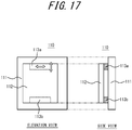
- FIG. 17 illustrates an elevation view and a side view of an attaching configuration 110 according to comparative example 2 in which a substrate 112 is attached to a housing 111.
- the attaching configuration 110 includes the housing 111, the substrate 112, and adhesives 113a, 113b.
- the housing 111 is a member having a rectangular plate-like shape when viewed from the front side.
- the substrate 112 has a rectangular exterior shape that is smaller than an exterior shape of the housing 111 when viewed from the front side.
- the housing 111 and the substrate 112 are arranged opposing each other. In a region where the substrate 112 and the housing 111 opposes each other between the housing 111 and the substrate 112, adhesives 113a and 113b are arranged along upper and lower surfaces of the substrate 112 when FIG. 17 is viewed from the front side.
- the substrate 112 can be shaken, for example, in up-down and left-right directions as indicated by double-headed arrows within its plane opposing the housing 111.
- a force in the shearing direction is applied to the adhesives 113a and 113b and may cause the adhesives 113a and 113b to be peeled off from the housing 111 and the substrate 112.
- FIG. 18 illustrates an elevation view, a cross-sectional view, and a side view of an attaching configuration 120 according to comparative example 3 in which a substrate 122 is attached to the housing 121.
- the attaching configuration 120 includes the housing 121, the substrate 122, and adhesives 123a to 123d.
- the housing 121 is a member having a rectangular plate-like shape.
- the housing 121 has protrusions 121a protruding along each side thereof to a side on which the substrate 122 is arranged.
- the substrate 122 is arranged in a region surrounded by the protrusions 121a, in a manner such that four peripheral surfaces thereof, which are sides when viewed from the front side, oppose respective inward-facing side surfaces of the protrusions 121a.
- the adhesives 123a to 123d are arranged in respective portions between the four peripheral surfaces of the substrate 122 and the inward-facing side surfaces of the protrusions 121a.
- the up-down direction when the elevation view illustrated in FIG. 18 is viewed from the front side corresponds to the vertical direction.
- a force in a tensile direction is applied to the adhesive 123a
- a force in a compression direction is applied to the adhesive 123b.
- a force in the shear direction is applied to the adhesive 123c and the adhesive 123d.
- the housing is enlarged.
- the substrate in the electronic apparatus can be attached without enlarging the housing.
- an imaging apparatus 10 serving as an electronic apparatus according to the embodiment of the present disclosure includes a substrate 11, a housing 12, an image sensor 13, and a lens 14 (an imaging optical system).
- the substrate 11 can be a printed circuit board having the image sensor 13 and circuit components 15 mounted thereon.
- the image sensor 13 and the circuit components 15 are fixed to the substrate 11 by soldering or the like. Although a number of circuit components 15 can be mounted on the substrate 11, only a few circuit components 15 are illustrated in FIG. 2 .
- the image sensor 13 includes a CCD image sensor (Charge-Coupled Device Image Sensor) or a CMOS image sensor (Complementary MOS Image Sensor).
- the image sensor 13 converts an image of a subject imaged by an optical system that includes the lens 14 into an electric signal.
- the image sensor 13 is arranged on a surface of the substrate 11 opposing the lens 14 in a manner such that an optical axis O of the lens 14 passes through the center of a light receiving surface.
- the circuit components 15 is configured to control the image sensor 13 and perform various processing on an electric signal that includes image information output from the image sensor 13.
- the processing performed by the circuit components 15 may include various image processing such as pixel interpolation processing, contrast adjustment, gamma correction, white balance adjustment, and the like.
- the housing 12 includes a lens barrel 12a and a base 12b.
- the lens barrel 12a holds the imaging optical system that includes the lens 14.
- the lens barrel 12a is a cylindrical portion that encloses the optical axis O of the lens 14.
- the lens 14 is not limited to one lens and may include a plurality of lenses.
- the lens 14 is configured to form an image of a subject on the light receiving surface of the image sensor 13.
- the lens barrel 12a can enclose optical elements such as a diaphragm, an IR cut filter, and the like, in addition to the lens 14.
- the base 12b is positioned at an edge of the lens barrel 12a and protrudes outward from the lens barrel 12a in a radial direction of the lens barrel.
- the base 12b has a three-dimensional configuration for enclosing the substrate 11. Further, the base 12b has a three-dimensional configuration for fixing other elements including a lid.
- the base 12b has a plate-like shape and may have a periphery similar to a rectangle shape.
- the substrate 11 has an approximate square shape, as illustrated in FIG. 3 .
- corners included in the approximate square shape opposing each other and their vicinity areas will be referred to as diagonal portions.
- a region having a distance from a vertex of one corner shorter than a vertex of another corner can be determined to be the vicinity area of the one corner.
- the vicinity area of the corner can be limited to a region further closer to the vertex of the corner.
- an intersection between extended lines of unremoved sides adjacent to the corner can be regarded as the vertex, and the corner and its vicinity area can be determined accordingly.
- a first diagonal portion 11a and a second diagonal portion 11b constituting a pair of diagonal portions of the substrate 11 respectively have a convex cut-off shape protruding in an in-plane direction of the substrate 11.
- the convex shape may include an arc shape obtained by dividing a circumference into four equal portions. That is, the first diagonal portion 11a and the second diagonal portion 11b respectively have a cut-off shape obtained by cutting off a quarter circle from a right-angled corner of the substrate 11.
- the base 12b of the housing 12 includes a first diagonal portion 12c and a second diagonal portion 12d respectively corresponding to the first diagonal portion 11a and the second diagonal portion 11b of the substrate 11.
- the first diagonal portion 12c includes a first protrusion 12e protruding in an arc in the normal of the surface of the substrate 11, along an end portion of the first diagonal portion 11a of the substrate 11 on a side opposite from a side having the lens 14 arranged thereon.
- the second diagonal portion 12d includes a second protrusion 12f protruding in an arc in the normal of the surface of the substrate 11, along an end portion of the second diagonal portion 11b of the substrate 11 on the side opposite from the side having the lens 14 arranged thereon.
- a screw hole 12g for attaching the lid of the imaging apparatus 10 may be formed on the outer side of the first protrusion 12e of the first diagonal portion 12c.
- the second diagonal portion 12d may include a screw hole 12h formed in a similar manner.
- FIG. 5 illustrates an enlarged view of a portion surrounded by two-dot chain lines illustrated in FIG. 3 .
- FIG. 6 illustrates an enlarged view of a portion surrounded by two-dot chain lines illustrated in FIG. 4 , by rotating the portion counterclockwise by 90 degrees.
- the first protrusion 12e has a first housing side surface 12i, which is a side surface opposing a first substrate side surface 11c serving as a side surface of the first diagonal portion 11a of the substrate 11.
- a distance between the first substrate side surface 11c and the first housing side surface 12i is approximately constant over an arcuate circumferential direction.
- An adhesive 16 is positioned between the side first substrate side surface 11c and the first housing side surface 12i.
- the adhesive 16 fixes the first substrate side surface 11c and the first housing side surface 12i by adhesion.
- an ultraviolet (UV) curable adhesive or a heat-curable adhesive is filled between the first substrate side surface 11c and the first housing side surface 12i.
- the adhesive 16 is irradiated with UV, or heated, to cure.
- the second diagonal portion 11b and the second protrusion 12f can also be fixed by adhesion.
- the optical axis O of the lens 14 is aligned with the center of the light receiving surface of the image sensor 13 before the adhesive 16 is cured, whereby the position of the substrate 11 may be adjusted with respect to the housing 12 in a direction along the surface of the substrate 11. Further, because an image formation position of the lens 14 is positioned on the light receiving surface of the image sensor 13, the position of the substrate 11 can be adjusted with respect to the housing 12 in the direction along the optical axis O.
- the adhesive 16 is filled between the first substrate side surface 11c and the first housing side surface 12i and between the second substrate side surface 11d and a second housing side surface 12j by using, for example, a syringe-shaped injection device having a fine tip.
- the adhesive 16 is somewhat viscous to stay in the gap.
- the ultraviolet (UV) curable adhesive is used as the adhesive 16, it can be cured by irradiating ultraviolet rays at the timing when the adhesive 16 is filled.
- the first diagonal portion 11a of the substrate 11 has the convex shape protruding in the in-plane direction.
- an orientation of the first substrate side surface 11c greatly differs between the first region 17a and the second region 17b located at either end of the first substrate side surface 11c in contact with the adhesive 16.
- the first region 17a includes a first adhesion position.
- the second region 17b includes a second adhesion position.
- "Orientation of the surface differs" can be rephrased as "Normal differs”.
- the normal of the first substrate side surface 11c can be different by approximately 90 degrees between the first region 17a and the second region 17b.
- the normal of the first housing side surface 12i of the first protrusion 12e opposing the first substrate side surface 11c can also be different by approximately 90 degrees between the first region 17a and the second region 17b.
- an orientation of the second substrate surface 11d greatly differs between the third region 17c and the fourth region 17d located at either end of the second substrate side surface 11d in contact with the adhesive 16.
- the third region 17c includes a third adhesion position.
- the fourth region 17d includes a fourth adhesion position.
- a normal of the side surface 11d may be different by approximately 90 degrees between the third region 17c and the fourth region 17d.
- a normal of the second housing side surface 12j of the second protrusion 12f opposing the side surface 11d can also differ by approximately 90 degrees between the third region 17c and the fourth region 17d.
- first substrate side surface 11c and the second substrate side surface 11d may be parallel to each other in the first region 17a and the third region 17c and in the second region 17b and the fourth region 17d. The same applies to the first housing side surface 12i and the second housing side surface 12j.
- the imaging apparatus 10 can reduce the size of the housing 12 and demonstrate excellent space saving properties.
- a contact direction of the adhesive 16 with respect to the first substrate side surface 11c in the first region 17a and a contact direction of the adhesive 16 with respect to the second substrate side surface 11d in the third region 17c are opposite to each other.
- the substrate 11 is held from both sides in the first region 17a and the third region 17c and thus suppressed from moving in a direction orthogonal to the first substrate side surface 11c and the second substrate side surface 11d.
- a contact direction of the adhesive 16 with respect to the first substrate side surface 11c in the second region 17b and a contact direction of the adhesive 16 with respect to the second substrate side surface 11d in the fourth region 17d are opposite to each other.
- the substrate 11 is held from both sides in the second region 17b and the fourth region 17d and thus suppressed from moving in the direction orthogonal to the first substrate side surface 11c and the second substrate side surface 11d. As a result, the substrate 11 is securely fixed to the housing 12.
- the orientation of the first substrate side surface 11c differs between the first region 17a and the second region 17b.
- the orientation of the second substrate side surface 11d differs between the third region 17c and the fourth region 17d. This configuration restricts a movement in the two directions, whereby the substrate 11 is more securely fixed to the housing 12. Further, because movements in the two directions at an angle of approximately 90 degrees from each other are restricted, the substrate 11 is particularly securely fixed to the housing 12.
- the adhesive 16 can be used to fix the substrate 11 to the housing 12 and, simultaneously, the possibility for peeling off or removal of the adhesive 16 due to a vibration or an impact can be suppressed.
- FIG. 8 and FIG. 9 are diagrams illustrating an adhesion state between the substrate 21 of the imaging apparatus 20 and the housing 22. Because a configuration of the imaging apparatus 20 is similar to the configuration of the imaging apparatus 10 illustrated in FIG. 1 to FIG. 7 , the same or similar elements are denoted by reference signs obtained by adding 10 to the reference signs of corresponding elements of the imaging apparatus 10. Hereinafter, a portion different from the imaging apparatus 10 will be described. Other portions are the same as those of the imaging apparatus 10, and descriptions thereof will thus be omitted.
- the imaging apparatus 20 has a shape in which the first diagonal portion 21a and the second diagonal portion 21b of the substrate 21 are cut off in a manner as to remove square portions from right-angled corners when FIG. 8 is viewed from the front side. It can be said that the first diagonal portion 21a and the second diagonal portion 21b of the substrate 21 have respective shapes cut off in a convex shape protruding in an in-plane direction of the substrate 21.
- the first substrate side surface 21c of the first diagonal portion 21a and the second substrate side surface 21d of the second diagonal portion 21b are respectively configured with two surfaces parallel to the horizontal and vertical directions when FIG. 8 is viewed from the front side. That is, the first substrate side surface 21c and the second substrate side surface 21d respectively have two surfaces in different orientations.
- a base 22b of the housing 22 has a first protrusion 22e and a second protrusion 22f protruding along the normal of the substrate 21 respectively from the first diagonal portion 22c and the second diagonal portion 22d toward the side on which the substrate 21 is provided.
- the first protrusion 22e has an inverted L-shape separated from the first substrate side surface 21c of the substrate 21 by a predetermined distance.
- the second protrusion 22f has an L-shape separated from the second substrate side surface 21d of the substrate 21 by a predetermined distance.
- the first protrusion 22e has a first housing side surface 22i opposing the first substrate side surface 21c.
- the second protrusion 22f has a second housing side surface 22j opposing the second substrate side surface 21d.
- the adhesive 26 is positioned between the first substrate side surface 21c and the first housing side surface 22i and between the second substrate side surface 21d and the second housing side surface 22j.
- the adhesive 26 positioned between the first substrate side surface 21c and the first housing side surface 22i has an L-shape or an inverted L-shape having the right-angled corner in the middle when FIG. 8 is viewed from the front side.
- contact directions of the adhesive 26 with respect to the substrate 21 are different by approximately 90 degrees between the first region 27a and the second region 27b located on different sides across the right-angled corner.
- contact directions of the adhesive 26 positioned between the second substrate side surface 21d and the second housing side surface 22j with respect to the substrate 21 are different by approximately 90 degrees between the third region 27c and the fourth region 27d located on different sides across the right-angled corner.
- the substrate 21 is fixed to the housing 22 by the adhesive 26 as described above.
- the adhesive 26 in a manner similar to the imaging apparatus 10, when a force caused by gravity or a vibration is applied to the adhesive 26, the force is distributed in a shearing direction, a compression direction, a pulling direction, and the like in each different regions of the adhesive 26.
- the possibility of peeling and removal of the adhesive 26 can be reduced.
- the housing 22 can be miniaturized and the space saving can be realized.
- the adhesive 26 in contact with the first substrate side surface 21c is separated into the first region 27a and the second region 27b across the right-angled corner.
- a length of the adhesive 26 in contact with the first substrate side surface 21c in the horizontal and vertical directions when FIG. 8 is viewed from the front side is longer than that of the imaging apparatus 10 having the first substrate side surface 11c formed from a curved surface.
- the first diagonal portion 21a and the second diagonal portion 21b of the substrate 21 have respective cut-off shapes at right angles protruding in the in-surface direction of the substrate 21 when viewed from the front side.
- the cut-off shapes of the first diagonal portion 21a and the second diagonal portion 21b are not limited thereto.
- the cut-off shapes of the first diagonal portion 21a and the second diagonal portion 21b may have an angle other than 90 degrees. That is, the first substrate side surface 21c and the second substrate side surface 21d do not need to be formed from two surfaces orthogonal to each other. Further, the first substrate side surface 21c and the second substrate side surface 21d may have a shape formed from three or more planes, rather than two planes.
- FIG. 10 and FIG. 11 are diagrams illustrating an adhesion state between a substrate 31 of the imaging apparatus 30 and a housing 32. Because a configuration of the imaging apparatus 30 is similar to the configuration of the imaging apparatus 10 illustrated in FIG. 1 to FIG. 7 , the same or similar elements are denoted by reference signs obtained by adding 20 to the reference signs of corresponding elements of the imaging apparatus 10. Hereinafter, a portion different from the imaging apparatus 10 will be described. Other portions are the same as those of the imaging apparatus 10, and descriptions thereof will thus be omitted.
- the substrate 31 of the imaging apparatus 30 has an approximate square shape and does not have a cut-off in the vicinity of each corner.
- the base 32b of the housing 32 of the imaging apparatus 30 does not have a protrusion.
- the base 32b has a recess 32k for accommodating the substrate 31.
- An inner side surface of the recess 32k, at least in a first diagonal portion 32c and a second diagonal portion 32d, is shaped in conformance with shapes of the first diagonal portion 31a and the second diagonal portion 31b of the substrate 31 having gaps therefrom.
- first housing side surface 32i An inner side of the recess 32k in the first diagonal portion 32c where the adhesive 36 is positioned, that is, a side surface opposing the substrate 31 will be referred to as a first housing side surface 32i.
- An inner side of the recess 32k in the second diagonal portion 32d where the adhesive 36 is positioned, that is, a side surface opposing the substrate 31 will be referred to as a second housing side surface 32j.
- first substrate side surface 31c of the first diagonal portion 31a and the second substrate side surface 31d of the second diagonal portion 31b respectively oppose the first housing side surface 32i and the second housing side surface 32j.
- the inner side surface of the recess 32k may be shaped in conformance with a periphery of the substrate 31 throughout the periphery of the substrate 31.
- the adhesive 36 is in contact with the first substrate side surface 31c and the first housing side surface 32i in the vertical direction in the first region 37a. Also, the adhesive 36 is in contact with the first substrate side surface 31c and the first housing side surface 32i in the horizontal direction in the second region 37b. The adhesive 36 is in contact with the second substrate side surface 31d and the second housing side surface 32j in the vertical direction in the third region 37c. The adhesive 36 is in contact with the second substrate side surface 31d and the second housing side surface 32j in the horizontal direction in the fourth region 37d.
- a contact direction of the adhesive 36 with respect to the first substrate side surface 31c in the first region 37a is opposite to a contact direction of the adhesive 36 with respect to the second substrate side surface 31d in the third region 37c.
- a contact direction of the adhesive 36 with respect to the first substrate side surface 31c in the second region 37b is opposite to a contact direction of the adhesive 36 with respect to the second substrate side surface 31d in the fourth region 37d.
- the contact direction or orientation of the adhesive with respect to any given surface is a direction that is orthogonal to the surface in contact with the adhesive and directed toward the contact surface from an adhesive side.
- the imaging apparatus 30 according to the example variation 2 can disperse a force caused by gravity or a vibration and reduce the possibility of peeling and removal of the adhesive 36, in a manner similar to the imaging apparatus 20.
- the substrate 31 can be securely fixed to the housing 32.
- the housing 32 can be miniaturized. For example, in the two diagonal portions other than the first diagonal portion 32c and the second diagonal portion 32d of the housing 32, the housing 32 does not need to protrude from the substrate 31 when viewed from the front side. Accordingly, the housing 32 can be miniaturized by removing the portions in the vicinity of the two corners other than the first diagonal portion 32c and the second diagonal portion 32d from the housing 32 illustrated in FIG. 10 .
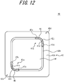
- FIG. 12 is a diagram illustrating an adhesion state between a substrate 41 of the imaging apparatus 40 and a housing 42. Because a configuration of the imaging apparatus 40 is similar to the configuration of the imaging apparatus 10 illustrated in FIG. 1 to FIG. 7 , the same or similar elements are denoted by reference signs obtained by adding 30 to the reference signs of corresponding elements of the imaging apparatus 10. Because the imaging apparatus 40 is particularly similar to the imaging apparatus 30 according to the example variation 2, a portion of the imaging apparatus 40 different from the imaging apparatus 30 will be described below.
- a first diagonal portion 41a and a second diagonal portion 41a of a substrate 41 have respective rounded quadrant shapes in the imaging apparatus 40 when FIG. 12 is viewed from the front side. That is, a first substrate side surface 41c and a second substrate side surface 41d respectively have partially curved surfaces similar to a cylindrical surface. Also, a first housing side surface 42i and a second housing side surface 42j of a recess 42k that are located on a housing side and respectively opposing the first substrate side surface 41c and the second substrate side surface 41d have partially curved surfaces similar to a cylindrical surface.
- An adhesive 46 is positioned between the first substrate side surface 41c and the first housing side surface 42i and between the second substrate side surface 41d and the second housing side surface 42j.
- the adhesive 46 positioned between the first substrate side surface 41c and the first housing side surface 42i is in contact with the first substrate side surface 41c and the first housing side surface 42i in the vertical direction when FIG. 12 is viewed from the front side.
- the adhesive 46 is in contact with the first substrate side surface 41c and the first housing side surface 42i in the vertical direction when FIG. 12 is viewed from the front side.
- the adhesive 46 positioned between the second substrate side surface 41d and the second housing side surface 42j is in contact with the second substrate side surface 41d and the second housing side surface 42j in the vertical direction when FIG.
- the imaging apparatus 40 according to the example variation 3 has an effect similar to the effect of the imaging apparatus 30 according to the example variation 2.
- the gap between the first substrate side surface 11c and the first housing side surface 12i having the adhesive 16 arranged therebetween is consistent in the extending direction of the adhesive 16, as illustrated in FIG. 5 by way of example.
- an imaging apparatus 50 according to the example variation 4 as illustrated in FIG. 13 a gap between a first substrate side surface 51c and a first housing side surface 52i varies in the extending direction of an adhesive 56. Because a configuration of the imaging apparatus 50 is similar to the configuration of the imaging apparatus 10 illustrated in FIG. 1 to FIG. 7 , the same or similar elements of the imaging apparatus 50 are denoted by reference signs obtained by adding 40 to the reference signs of corresponding elements of the imaging apparatus 10, and a portion different from the imaging apparatus 10 will be described.
- FIG. 13 illustrates an arrangement of the adhesive 56 between a first diagonal portion 51a of a substrate 51 and a first diagonal portion 52c of a housing 52.
- End portions of a region in which the adhesive 56 is positioned in FIG. 13 will be respectively referred to as a first end portion 58a and a second end portion 58b.
- a middle portion located between the first end portion 58a and the second end portion 58b will be referred to as a middle portion 58c.
- the first end 58a and the second end 58b are narrower than the middle portion 58c.
- This configuration can restrict a movement of the adhesive 56 in its extending direction when the adhesive 56 of the imaging apparatus 50 is at least partially peeled off from the first substrate side surface 51c and/or the first housing side surface 52i. That is, because a gap between the first substrate side surface 51c and the first housing side surface 52i is reduced, the adhesive 56 positioned in the middle portion 58c is restricted from moving to the first end portion 58a or the second end portion 58b.
- a second diagonal portion 51b of the substrate 51 and a second diagonal portion 52d of the housing 52 can be configured in a similar manner.
- the adhesive 56 positioned between the second diagonal portion 51b and the second diagonal portion 52d is also restricted from moving along the extending direction of the adhesive 56.
- the imaging apparatus 50 according to the example variation 4 demonstrates the effect of the imaging apparatus 10 and, further, restricts the movement of the adhesive 56 as described above, whereby the peeling occurred in a portion of the adhesive 56 is suppressed from extending to another portion. Also, the possibility that the adhesive 56 being peeled off moves in the gap between the first diagonal portion 51a and the first diagonal portion 52c and separates from between the first diagonal portion 51a and the first diagonal portion 52c can be reduced.
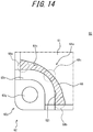
- An imaging apparatus 60 according to the example variation 5 is different from the imaging apparatus 50 according to the example variation 4, in terms of a thickness distribution of an adhesive 66 alone.
- Elements of the imaging apparatus 60 that are the same as or similar to elements of the imaging apparatus 10 are denoted by reference signs obtained by adding 50 to the reference signs of corresponding elements of the imaging apparatus 10, and descriptions thereof will thus be omitted.
- a gap between a first substrate side surface 61c and a first housing side surface 62i is longer in a first end portion 68a and a second end portion 68b than in a middle portion 68c, as illustrated in FIG. 14 .
- the adhesive 66 is restricted from moving in the extending direction thereof. That is, due to the reduced gap between the first substrate side surface 61c and the first housing side surface 62i, the adhesive 66 positioned at the first end portion 68a and the second end portion 68b is restricted from moving to the middle portion 68c.
- a second diagonal portion 61b of a substrate 61 and a second diagonal portion 62d of a housing 62 can be configured in a similar manner.
- the adhesive 66 positioned between the second diagonal portion 61b and the second diagonal portion 62d is also restricted from moving along the extending direction of the adhesive 66.
- the imaging apparatus 60 demonstrates the effect of the imaging apparatus 10 and, further, when a part of the adhesive 66 is peeled off, the imaging apparatus 60 suppresses a peeled portion from extending to another portion, in a manner similar to the imaging apparatus 50 according to the example variation 4. Further, the imaging apparatus 60 reduces the possibility that the adhesive 66 being peeled off separates from the adhesion position.
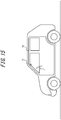
- FIG. 15 illustrates an example in which an imaging apparatus 71 serving as one of the imaging apparatuses of the present disclosure is arranged on an inner side of a windshield of a vehicle 70 (the mobile body).
- the imaging apparatus 71 can take an image of a subject located in front of the vehicle 70 through the windshield.
- An installation position of the imaging apparatus 71 illustrated in FIG. 15 is merely an example.
- the imaging apparatus 71 can be installed at various positions in a manner having the optical axis directed in various directions.
- the imaging apparatus 71 may be fixed to any one of a front bumper, a front grill, a lighting module, a side mirror, a rear bumper, or the like of the vehicle.
- vehicle encompasses, for example, vehicles, ships, and aircrafts.
- vehicle as used herein encompasses, but is not limited to, automobiles, rail vehicles, industrial vehicles, and domestic vehicles.
- the vehicle may include fixed wing aircrafts that travel on a runway.
- Automobiles include cars, trucks, buses, motorcycles, and trolley buses, but are not limited thereto and may also include other automobiles that travel on the road.
- Rail vehicles include locomotives, freight cars, passenger cars, trams, guided track railroads, ropeways, cable cars, linear motor cars and monorails, but are not limited thereto and may also include other vehicles that travel on the track.
- Industrial vehicles include agricultural vehicles and construction vehicles.
- Industrial vehicles include, but are not limited to, forklifts and golf carts.
- Industrial vehicles for agricultural purpose include, but are not limited to, tractors, tillers, transplanters, binders, combined harvesters, and lawn mowers.
- Industrial vehicles for construction purposes include, but are not limited to, bulldozers, scrapers, excavators, crane trucks, dump trucks, and load rollers.
- Life vehicles may include, but are not limited to, bicycles, wheelchairs, strollers, wheelbarrows, electric standing two-wheeled vehicles.
- Power engines of vehicles include, but are not limited to, internal combustion engines including diesel engines, gasoline engines, and hydrogen engines, and electric engines including motors.
- Vehicles include human-power vehicles traveling on human power. Classification of the vehicles is not limited to the above. For example, vehicles may include industrial vehicles authorized to travel on the road, and a plurality of categories may include the same type of vehicle.
- an imaging apparatus is used as the electronic apparatus in the above embodiment.
- the electronic apparatus is not limited to the imaging apparatus.
- the present disclosure can be applied to various electronic apparatuses.
- the electronic apparatus can be a mobile phone, a portable information terminal, a portable music player, an in-vehicle navigation device, an in-vehicle sensor device, or the like.
- the optical system including the lens and the image sensor are not essential.
- the housing does not need to include the lens barrel.
Landscapes
- Engineering & Computer Science (AREA)
- Physics & Mathematics (AREA)
- Multimedia (AREA)
- Signal Processing (AREA)
- General Physics & Mathematics (AREA)
- Microelectronics & Electronic Packaging (AREA)
- Mechanical Engineering (AREA)
- Optics & Photonics (AREA)
- Studio Devices (AREA)
- Camera Bodies And Camera Details Or Accessories (AREA)
- Lens Barrels (AREA)
- Casings For Electric Apparatus (AREA)
- Mounting Of Printed Circuit Boards And The Like (AREA)
Abstract
Description
- This application claims priority to and the benefit of
Japanese Patent Application No. 2018-159392 filed on August 28, 2018 - The present disclosure relates to an electronic apparatus, an imaging apparatus, and a mobile body.
- In electronic apparatuses, screws are generally used to fix a substrate having circuit components mounted thereon to a housing. However, in a case in which the screws are used for fixing, when the screws are tightened, a force may be applied between the substrate and the housing and may inhibit maintaining the accuracy of a mounting position. For this reason, it has been proposed to use an adhesive to fix the substrate and the housing. For example, in PTL1 set forth below, a convex portion is provided in an enclosure portion on a housing side for enclosing a substrate, and an adhesive is applied to the convex portion to attach the substrate having electronic components mounted thereon.
- PTL 1:
JP-A-2003-108968 - An electronic apparatus according to the present disclosure includes a substrate, a housing, and an adhesive. The housing has opposing surfaces respectively opposing side surfaces of a pair of diagonal portions of the substrate and encloses the substrate. The adhesive is positioned between the side surfaces of the pair of diagonal portions of the substrate and the opposing surfaces of the housing.
- An imaging apparatus according to the present disclosure includes an imaging optical system, an image sensor, a substrate, a housing, and an adhesive. The image sensor converts an image of a subject formed by the imaging optical system into an electric signal. The substrate has a circuit component including the image sensor mounted thereon. The housing supports the imaging optical system, has opposing surfaces opposing respective side surfaces of a pair of diagonal portions of the substrate, and encloses the substrate. The adhesive is positioned between the side surfaces of the pair of diagonal portions of the substrate and the opposing surfaces of the housing.
- A mobile body according to the present disclosure is equipped with an imaging apparatus. The imaging apparatus includes an imaging optical system, an image sensor, a substrate, a housing, and an adhesive. The image sensor converts an image of a subject formed by the imaging optical system into an electric signal. The substrate has the image sensor mounted thereon. The housing supports the imaging optical system, has opposing surfaces opposing respective side surfaces of a pair of diagonal portions of the substrate, and encloses the substrate. The adhesive is positioned between the side surfaces of the pair of diagonal portions of the substrate and the opposing surfaces of the housing.
- In the accompanying drawings:
-
FIG. 1 is an exploded perspective view of a portion of an imaging apparatus according to an embodiment; -
FIG. 2 is a perspective view of the imaging apparatus illustrated inFIG. 1 as viewed from a diagonally rear side thereof; -
FIG. 3 is a diagram illustrating the imaging apparatus illustratedFIG. 1 as viewed from a substrate side; -
FIG. 4 is a cross-sectional view taken from line A-A ofFIG. 3 ; -
FIG. 5 is an enlarged view of a first diagonal portion illustrated inFIG. 3 ; -
FIG. 6 is an enlarged cross-sectional view of the first diagonal portion illustrated inFIG. 4 ; -
FIG. 7 is a diagram illustrating an adhesion state between a housing and a substrate in the imaging apparatus illustrated inFIG. 1 ; -
FIG. 8 is a diagram illustrating an adhesion state between a housing and a substrate in an imaging apparatus according to an example variation 1; -
FIG. 9 is a cross-sectional view taken from line B-B ofFIG. 8 ; -
FIG. 10 is a diagram illustrating an adhesion state between a housing and a substrate in an imaging apparatus according to an example variation 2; -
FIG. 11 is a cross-sectional view taken from line C-C ofFIG. 10 ; -
FIG. 12 is a diagram illustrating an adhesion state between a housing and a substrate in an imaging apparatus according to an example variation 3; -
FIG. 13 is an enlarged view of a first diagonal portion of an imaging apparatus according to an example variation 4; -
FIG. 14 is an enlarged view of a first diagonal portion of an imaging apparatus according to anexample variation 5; -
FIG. 15 is a diagram illustrating an example for mounting an imaging apparatus on a vehicle; -
FIG. 16 is a diagram illustrating an adhesion state between a housing and a substrate according to comparative example 1; -
FIG. 17 is a diagram illustrating an adhesion state between a housing and a substrate according to comparative example 2; and -
FIG. 18 is a diagram illustrating an adhesion state between a housing and a substrate according to comparative example 3. - Electronic apparatuses may be used in an environment subject to vibrations, including a position in a mobile body such as a vehicle. Also, the electronic apparatuses may be carried by people during walking or exercising and subjected to an impact caused by a drop or collision thereof while being used. In a case in which a substrate is fixed to a housing by an adhesive, there is a concern that, upon application of a vibration or an impact to the electronic apparatus, a stress caused by the vibration or the impact converges at a particular position on an adhesion surface, causing peeling. In particular, in a case in which the electronic component mounted on the substrate has a heavy weight, the stress applied to the adhesion surface when subjected to the vibration or impact increases, and there is a great risk of the peeling of the adhesive.
- The present disclosure relates to an electronic apparatus that uses an adhesive to secure a substrate to a housing and is capable of reducing the possibility of the peeling of the adhesive caused by a vibration or an impact, an imaging apparatus, and a vehicle having the electronic apparatus and the imaging apparatus mounted thereon.
- Prior to descriptions of the electronic apparatuses and the like according to the present disclosure, configurations of comparative examples assumed to be methods for fixing the substrate and the housing using an adhesive will be described.
-
FIG. 16 illustrates an elevation view and a side view of an attachingconfiguration 100 according to comparative example 1 in which asubstrate 102 is attached to ahousing 101. The attachingconfiguration 100 includes thehousing 101, thesubstrate 102, andadhesives FIG. 16 and other drawings, the adhesives are highlighted by shading. - The
housing 101 is a member having a rectangular plate-like shape when viewed from a front side. Thehousing 101 includes a pair ofprotrusions 101a protruding to a side having thesubstrate 102 provided thereon, along upper and lower sides of thehousing 101 whenFIG. 16 is viewed from the front side. Thesubstrate 102 is a rectangular substrate having a circuit component mounted thereon. Thesubstrate 102 is arranged between theprotrusions 101a in a manner such that upper and lower surfaces of thesubstrate 102 opposecorresponding protrusions 101a whenFIG. 16 is viewed from the front side. - The adhesive 103a is positioned between the
protrusion 101a on the upper side of thehousing 101 illustrated inFIG. 16 and the upper surface of thesubstrate 102. The adhesive 103b is positioned between the protrusion 101b on the lower side of thehousing 101 illustrated inFIG. 16 and the lower surface of thesubstrate 102. Theadhesives substrate 102 to thehousing 101. As theadhesives - When the attaching
configuration 100 of the electronic apparatus illustrated inFIG. 16 is subjected to a vibration or an impact, thesubstrate 102 can be shaken, for example, in a direction parallel to an extending direction of theprotrusion 101a of thehousing 101, as indicated by a double-headed arrow. In this case, theadhesives protrusions 101a of thehousing 101 and thesubstrate 102. The shearing direction means two opposing directions that extend along an adhesion surface across the adhesion surface attached by the adhesive. -
FIG. 17 illustrates an elevation view and a side view of an attachingconfiguration 110 according to comparative example 2 in which asubstrate 112 is attached to ahousing 111. The attachingconfiguration 110 includes thehousing 111, thesubstrate 112, andadhesives housing 111 is a member having a rectangular plate-like shape when viewed from the front side. Thesubstrate 112 has a rectangular exterior shape that is smaller than an exterior shape of thehousing 111 when viewed from the front side. Thehousing 111 and thesubstrate 112 are arranged opposing each other. In a region where thesubstrate 112 and thehousing 111 opposes each other between thehousing 111 and thesubstrate 112,adhesives substrate 112 whenFIG. 17 is viewed from the front side. - When the attaching
configuration 110 of the electronic apparatus illustrated inFIG. 17 is subjected to a vibration or an impact, thesubstrate 112 can be shaken, for example, in up-down and left-right directions as indicated by double-headed arrows within its plane opposing thehousing 111. In this case, a force in the shearing direction is applied to theadhesives adhesives housing 111 and thesubstrate 112. -
FIG. 18 illustrates an elevation view, a cross-sectional view, and a side view of an attachingconfiguration 120 according to comparative example 3 in which asubstrate 122 is attached to thehousing 121. The attachingconfiguration 120 includes thehousing 121, thesubstrate 122, andadhesives 123a to 123d. Thehousing 121 is a member having a rectangular plate-like shape. Thehousing 121 hasprotrusions 121a protruding along each side thereof to a side on which thesubstrate 122 is arranged. Thesubstrate 122 is arranged in a region surrounded by theprotrusions 121a, in a manner such that four peripheral surfaces thereof, which are sides when viewed from the front side, oppose respective inward-facing side surfaces of theprotrusions 121a. Theadhesives 123a to 123d are arranged in respective portions between the four peripheral surfaces of thesubstrate 122 and the inward-facing side surfaces of theprotrusions 121a. - In the attaching
configuration 120 according to comparative example 3, for example, the up-down direction when the elevation view illustrated inFIG. 18 is viewed from the front side corresponds to the vertical direction. Upon application of a load to thesubstrate 122 in a downward direction indicated by an arrow G, a force in a tensile direction is applied to the adhesive 123a, and a force in a compression direction is applied to the adhesive 123b. Simultaneously, a force in the shear direction is applied to the adhesive 123c and the adhesive 123d. As a result, when thesubstrate 122 is subjected to a vibration or an impact, a stress is separated into a shearing force, a compressive force, and a tensile force in theadhesives 123a to 123d. Thus, a convergent application of the stress to a particular one of theadhesives 123a to 123d can be avoided. - In the attaching
configuration 120 of the electronic apparatus illustrated inFIG. 18 , however, because thesubstrate 122 needs to be covered in all directions along four peripheral surfaces thereof, the housing is enlarged. Preferably, the substrate in the electronic apparatus can be attached without enlarging the housing. - Hereinafter, an embodiment of the present disclosure will be described with reference to the drawings. The drawings used herein are merely schematic. The drawings are not necessarily drawn to scale. In the following description, further, terms such as upper, lower, horizontal, and vertical may be used as respective directions when the drawings are viewed from the front side. However, such directions are not limited to the vertical or horizontal direction in relation to gravity, unless otherwise specified. The "upper" and "lower" can be interchanged, and the "horizontal" and "vertical" can also be interchanged, as desired.
- As illustrated in an exploded perspective view in
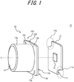
FIG. 1 and a perspective view inFIG. 2 , animaging apparatus 10 serving as an electronic apparatus according to the embodiment of the present disclosure includes asubstrate 11, ahousing 12, animage sensor 13, and a lens 14 (an imaging optical system). - The
substrate 11 can be a printed circuit board having theimage sensor 13 andcircuit components 15 mounted thereon. Theimage sensor 13 and thecircuit components 15 are fixed to thesubstrate 11 by soldering or the like. Although a number ofcircuit components 15 can be mounted on thesubstrate 11, only afew circuit components 15 are illustrated inFIG. 2 . - The
image sensor 13 includes a CCD image sensor (Charge-Coupled Device Image Sensor) or a CMOS image sensor (Complementary MOS Image Sensor). Theimage sensor 13 converts an image of a subject imaged by an optical system that includes thelens 14 into an electric signal. Thus, theimage sensor 13 is arranged on a surface of thesubstrate 11 opposing thelens 14 in a manner such that an optical axis O of thelens 14 passes through the center of a light receiving surface. - The
circuit components 15 is configured to control theimage sensor 13 and perform various processing on an electric signal that includes image information output from theimage sensor 13. The processing performed by thecircuit components 15 may include various image processing such as pixel interpolation processing, contrast adjustment, gamma correction, white balance adjustment, and the like. - The
housing 12 includes alens barrel 12a and abase 12b. - The
lens barrel 12a holds the imaging optical system that includes thelens 14. Thelens barrel 12a is a cylindrical portion that encloses the optical axis O of thelens 14. Thelens 14 is not limited to one lens and may include a plurality of lenses. Thelens 14 is configured to form an image of a subject on the light receiving surface of theimage sensor 13. Thelens barrel 12a can enclose optical elements such as a diaphragm, an IR cut filter, and the like, in addition to thelens 14. - The
base 12b is positioned at an edge of thelens barrel 12a and protrudes outward from thelens barrel 12a in a radial direction of the lens barrel. Thebase 12b has a three-dimensional configuration for enclosing thesubstrate 11. Further, thebase 12b has a three-dimensional configuration for fixing other elements including a lid. For example, thebase 12b has a plate-like shape and may have a periphery similar to a rectangle shape. Hereinafter, a configuration in which thesubstrate 11 is fixed to the base 12b of thehousing 12 will be described with reference toFIG. 3 to FIG. 6 . - The
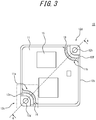
substrate 11 has an approximate square shape, as illustrated inFIG. 3 . In the present application, corners included in the approximate square shape opposing each other and their vicinity areas will be referred to as diagonal portions. A region having a distance from a vertex of one corner shorter than a vertex of another corner can be determined to be the vicinity area of the one corner. The vicinity area of the corner can be limited to a region further closer to the vertex of the corner. In a case in which a vertex area of a corner is removed as cut-off or the like, an intersection between extended lines of unremoved sides adjacent to the corner can be regarded as the vertex, and the corner and its vicinity area can be determined accordingly. - A first
diagonal portion 11a and a seconddiagonal portion 11b constituting a pair of diagonal portions of thesubstrate 11 respectively have a convex cut-off shape protruding in an in-plane direction of thesubstrate 11. In theimaging apparatus 10, the convex shape may include an arc shape obtained by dividing a circumference into four equal portions. That is, the firstdiagonal portion 11a and the seconddiagonal portion 11b respectively have a cut-off shape obtained by cutting off a quarter circle from a right-angled corner of thesubstrate 11. - The base 12b of the
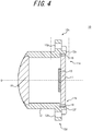
housing 12 includes a firstdiagonal portion 12c and a seconddiagonal portion 12d respectively corresponding to the firstdiagonal portion 11a and the seconddiagonal portion 11b of thesubstrate 11. As illustrated inFIG. 3 andFIG. 4 , the firstdiagonal portion 12c includes afirst protrusion 12e protruding in an arc in the normal of the surface of thesubstrate 11, along an end portion of the firstdiagonal portion 11a of thesubstrate 11 on a side opposite from a side having thelens 14 arranged thereon. Similarly, the seconddiagonal portion 12d includes asecond protrusion 12f protruding in an arc in the normal of the surface of thesubstrate 11, along an end portion of the seconddiagonal portion 11b of thesubstrate 11 on the side opposite from the side having thelens 14 arranged thereon. Ascrew hole 12g for attaching the lid of theimaging apparatus 10 may be formed on the outer side of thefirst protrusion 12e of the firstdiagonal portion 12c. The seconddiagonal portion 12d may include ascrew hole 12h formed in a similar manner. -
FIG. 5 illustrates an enlarged view of a portion surrounded by two-dot chain lines illustrated inFIG. 3 . Also,FIG. 6 illustrates an enlarged view of a portion surrounded by two-dot chain lines illustrated inFIG. 4 , by rotating the portion counterclockwise by 90 degrees. As illustrated in the enlarged views ofFIG. 5 andFIG. 6 , thefirst protrusion 12e has a firsthousing side surface 12i, which is a side surface opposing a firstsubstrate side surface 11c serving as a side surface of the firstdiagonal portion 11a of thesubstrate 11. As illustrated inFIG. 5 , a distance between the firstsubstrate side surface 11c and the firsthousing side surface 12i is approximately constant over an arcuate circumferential direction. - An adhesive 16 is positioned between the side first
substrate side surface 11c and the firsthousing side surface 12i. The adhesive 16 fixes the firstsubstrate side surface 11c and the firsthousing side surface 12i by adhesion. In particular, at the time of manufacturing of theimaging apparatus 10, an ultraviolet (UV) curable adhesive or a heat-curable adhesive is filled between the firstsubstrate side surface 11c and the firsthousing side surface 12i. After filling the adhesive 16, the adhesive 16 is irradiated with UV, or heated, to cure. The seconddiagonal portion 11b and thesecond protrusion 12f can also be fixed by adhesion. - There are gaps between the first
diagonal portion 11a of thesubstrate 11 and thefirst protrusion 12e of thehousing 12 and between the seconddiagonal portion 11b of thesubstrate 11 and thesecond protrusion 12f of thehousing 12. There is also a gap between the surface of thesubstrate 11 on the side of thelens 14 and the surface of thehousing 12 opposing thebase 12b. Thus, at the time of manufacturing of theimaging apparatus 10, the optical axis O of thelens 14 is aligned with the center of the light receiving surface of theimage sensor 13 before the adhesive 16 is cured, whereby the position of thesubstrate 11 may be adjusted with respect to thehousing 12 in a direction along the surface of thesubstrate 11. Further, because an image formation position of thelens 14 is positioned on the light receiving surface of theimage sensor 13, the position of thesubstrate 11 can be adjusted with respect to thehousing 12 in the direction along the optical axis O. - After adjusting the positions of the
substrate 11 and thehousing 12, the adhesive 16 is filled between the firstsubstrate side surface 11c and the firsthousing side surface 12i and between the secondsubstrate side surface 11d and a secondhousing side surface 12j by using, for example, a syringe-shaped injection device having a fine tip. Preferably, the adhesive 16 is somewhat viscous to stay in the gap. In a case in which the ultraviolet (UV) curable adhesive is used as the adhesive 16, it can be cured by irradiating ultraviolet rays at the timing when the adhesive 16 is filled. - Next, an effect of the attaching configuration of the
substrate 11 on thehousing 12 in theimaging apparatus 10 will be described with reference toFIG. 7 . The firstdiagonal portion 11a of thesubstrate 11 has the convex shape protruding in the in-plane direction. Thus, an orientation of the firstsubstrate side surface 11c greatly differs between thefirst region 17a and thesecond region 17b located at either end of the firstsubstrate side surface 11c in contact with the adhesive 16. Thefirst region 17a includes a first adhesion position. Thesecond region 17b includes a second adhesion position. "Orientation of the surface differs" can be rephrased as "Normal differs". For example, the normal of the firstsubstrate side surface 11c can be different by approximately 90 degrees between thefirst region 17a and thesecond region 17b. Further, the normal of the firsthousing side surface 12i of thefirst protrusion 12e opposing the firstsubstrate side surface 11c can also be different by approximately 90 degrees between thefirst region 17a and thesecond region 17b. - In a manner similar to the first
diagonal portion 11a, in the seconddiagonal portion 11b an orientation of thesecond substrate surface 11d greatly differs between thethird region 17c and thefourth region 17d located at either end of the secondsubstrate side surface 11d in contact with the adhesive 16. Thethird region 17c includes a third adhesion position. Thefourth region 17d includes a fourth adhesion position. For example, a normal of theside surface 11d may be different by approximately 90 degrees between thethird region 17c and thefourth region 17d. Further, a normal of the secondhousing side surface 12j of thesecond protrusion 12f opposing theside surface 11d can also differ by approximately 90 degrees between thethird region 17c and thefourth region 17d. - Further, the first
substrate side surface 11c and the secondsubstrate side surface 11d may be parallel to each other in thefirst region 17a and thethird region 17c and in thesecond region 17b and thefourth region 17d. The same applies to the firsthousing side surface 12i and the secondhousing side surface 12j. - As described above, in a case in which the
substrate 11 is fixed to the base 12b of thehousing 12, when, for example, gravity or a vertical vibration in the vertical direction indicated by the arrow G is applied to thesubstrate 11, a force in the shear direction is applied to thefirst region 17a and thethird region 17c. On the other hand, compression or a force in a tensile direction is applied to thesecond region 17b and thefourth region 17d. Alternatively, when gravity or a vibration in the direction orthogonal to the arrow G is applied, a force in the shearing direction is applied to thesecond region 17b and thefourth region 17d, and compression or a force in a tensile direction is applied to thefirst region 17a and thethird region 17c. As a result, the stress applied to the adhesive 16 can be dispersed, whereby the possibility of peeling off and removal of the adhesive 16 can be reduced. Further, because the adhesion is performed in the pair of diagonal portions of thesubstrate 11 alone, the adhesive 16 does not need to cover the periphery of thesubstrate 11 in its entirety. Accordingly, theimaging apparatus 10 can reduce the size of thehousing 12 and demonstrate excellent space saving properties. - Further, a contact direction of the adhesive 16 with respect to the first
substrate side surface 11c in thefirst region 17a and a contact direction of the adhesive 16 with respect to the secondsubstrate side surface 11d in thethird region 17c are opposite to each other. Thus, thesubstrate 11 is held from both sides in thefirst region 17a and thethird region 17c and thus suppressed from moving in a direction orthogonal to the firstsubstrate side surface 11c and the secondsubstrate side surface 11d. Further, a contact direction of the adhesive 16 with respect to the firstsubstrate side surface 11c in thesecond region 17b and a contact direction of the adhesive 16 with respect to the secondsubstrate side surface 11d in thefourth region 17d are opposite to each other. Thus, thesubstrate 11 is held from both sides in thesecond region 17b and thefourth region 17d and thus suppressed from moving in the direction orthogonal to the firstsubstrate side surface 11c and the secondsubstrate side surface 11d. As a result, thesubstrate 11 is securely fixed to thehousing 12. - In the example illustrated in
FIG. 7 , further, the orientation of the firstsubstrate side surface 11c differs between thefirst region 17a and thesecond region 17b. Also, the orientation of the secondsubstrate side surface 11d differs between thethird region 17c and thefourth region 17d. This configuration restricts a movement in the two directions, whereby thesubstrate 11 is more securely fixed to thehousing 12. Further, because movements in the two directions at an angle of approximately 90 degrees from each other are restricted, thesubstrate 11 is particularly securely fixed to thehousing 12. - According to the imaging apparatus 10 (the electronic apparatus) of the present disclosure, as described above, the adhesive 16 can be used to fix the
substrate 11 to thehousing 12 and, simultaneously, the possibility for peeling off or removal of the adhesive 16 due to a vibration or an impact can be suppressed. - Next, an
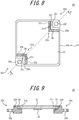
imaging apparatus 20 according to the example variation 1 will be described with reference toFIG. 8 and FIG. 9. FIG. 8 and FIG. 9 are diagrams illustrating an adhesion state between thesubstrate 21 of theimaging apparatus 20 and thehousing 22. Because a configuration of theimaging apparatus 20 is similar to the configuration of theimaging apparatus 10 illustrated inFIG. 1 to FIG. 7 , the same or similar elements are denoted by reference signs obtained by adding 10 to the reference signs of corresponding elements of theimaging apparatus 10. Hereinafter, a portion different from theimaging apparatus 10 will be described. Other portions are the same as those of theimaging apparatus 10, and descriptions thereof will thus be omitted. - The
imaging apparatus 20 has a shape in which the firstdiagonal portion 21a and the seconddiagonal portion 21b of thesubstrate 21 are cut off in a manner as to remove square portions from right-angled corners whenFIG. 8 is viewed from the front side. It can be said that the firstdiagonal portion 21a and the seconddiagonal portion 21b of thesubstrate 21 have respective shapes cut off in a convex shape protruding in an in-plane direction of thesubstrate 21. Thus, the firstsubstrate side surface 21c of the firstdiagonal portion 21a and the secondsubstrate side surface 21d of the seconddiagonal portion 21b are respectively configured with two surfaces parallel to the horizontal and vertical directions whenFIG. 8 is viewed from the front side. That is, the firstsubstrate side surface 21c and the secondsubstrate side surface 21d respectively have two surfaces in different orientations. - A base 22b of the
housing 22 has afirst protrusion 22e and asecond protrusion 22f protruding along the normal of thesubstrate 21 respectively from the firstdiagonal portion 22c and the seconddiagonal portion 22d toward the side on which thesubstrate 21 is provided. Thefirst protrusion 22e has an inverted L-shape separated from the firstsubstrate side surface 21c of thesubstrate 21 by a predetermined distance. Thesecond protrusion 22f has an L-shape separated from the secondsubstrate side surface 21d of thesubstrate 21 by a predetermined distance. Thefirst protrusion 22e has a firsthousing side surface 22i opposing the firstsubstrate side surface 21c. Thesecond protrusion 22f has a secondhousing side surface 22j opposing the secondsubstrate side surface 21d. - The adhesive 26 is positioned between the first
substrate side surface 21c and the firsthousing side surface 22i and between the secondsubstrate side surface 21d and the secondhousing side surface 22j. The adhesive 26 positioned between the firstsubstrate side surface 21c and the firsthousing side surface 22i has an L-shape or an inverted L-shape having the right-angled corner in the middle whenFIG. 8 is viewed from the front side. Thus, contact directions of the adhesive 26 with respect to thesubstrate 21 are different by approximately 90 degrees between thefirst region 27a and thesecond region 27b located on different sides across the right-angled corner. Similarly, contact directions of the adhesive 26 positioned between the secondsubstrate side surface 21d and the secondhousing side surface 22j with respect to thesubstrate 21 are different by approximately 90 degrees between thethird region 27c and thefourth region 27d located on different sides across the right-angled corner. - In the
imaging apparatus 20 according to the present disclosure, thesubstrate 21 is fixed to thehousing 22 by the adhesive 26 as described above. Thus, in a manner similar to theimaging apparatus 10, when a force caused by gravity or a vibration is applied to the adhesive 26, the force is distributed in a shearing direction, a compression direction, a pulling direction, and the like in each different regions of the adhesive 26. As a result, the possibility of peeling and removal of the adhesive 26 can be reduced. Further, because a pair of diagonal portions of thesubstrate 21 alone are adhered, thehousing 22 can be miniaturized and the space saving can be realized. - In the
imaging apparatus 20, further, the adhesive 26 in contact with the firstsubstrate side surface 21c is separated into thefirst region 27a and thesecond region 27b across the right-angled corner. Thus, a length of the adhesive 26 in contact with the firstsubstrate side surface 21c in the horizontal and vertical directions whenFIG. 8 is viewed from the front side is longer than that of theimaging apparatus 10 having the firstsubstrate side surface 11c formed from a curved surface. The same applies to the secondsubstrate side surface 21d. Because the adhesive 26 highly effectively restricts movements in the horizontal and vertical directions orthogonal to each other, thesubstrate 21 is more securely fixed to thehousing 22 in theimaging apparatus 20. - In the example variation 1 described above, the first
diagonal portion 21a and the seconddiagonal portion 21b of thesubstrate 21 have respective cut-off shapes at right angles protruding in the in-surface direction of thesubstrate 21 when viewed from the front side. However, the cut-off shapes of the firstdiagonal portion 21a and the seconddiagonal portion 21b are not limited thereto. The cut-off shapes of the firstdiagonal portion 21a and the seconddiagonal portion 21b may have an angle other than 90 degrees. That is, the firstsubstrate side surface 21c and the secondsubstrate side surface 21d do not need to be formed from two surfaces orthogonal to each other. Further, the firstsubstrate side surface 21c and the secondsubstrate side surface 21d may have a shape formed from three or more planes, rather than two planes. - An
imaging apparatus 30 according to the example variation 2 will be described with reference toFIG. 10 and FIG. 11. FIG. 10 and FIG. 11 are diagrams illustrating an adhesion state between asubstrate 31 of theimaging apparatus 30 and ahousing 32. Because a configuration of theimaging apparatus 30 is similar to the configuration of theimaging apparatus 10 illustrated inFIG. 1 to FIG. 7 , the same or similar elements are denoted by reference signs obtained by adding 20 to the reference signs of corresponding elements of theimaging apparatus 10. Hereinafter, a portion different from theimaging apparatus 10 will be described. Other portions are the same as those of theimaging apparatus 10, and descriptions thereof will thus be omitted. - As illustrated in
FIG. 10 and FIG. 11 , thesubstrate 31 of theimaging apparatus 30 has an approximate square shape and does not have a cut-off in the vicinity of each corner. Further, thebase 32b of thehousing 32 of theimaging apparatus 30 does not have a protrusion. Thebase 32b has arecess 32k for accommodating thesubstrate 31. An inner side surface of therecess 32k, at least in a firstdiagonal portion 32c and a seconddiagonal portion 32d, is shaped in conformance with shapes of the firstdiagonal portion 31a and the seconddiagonal portion 31b of thesubstrate 31 having gaps therefrom. An inner side of therecess 32k in the firstdiagonal portion 32c where the adhesive 36 is positioned, that is, a side surface opposing thesubstrate 31 will be referred to as a firsthousing side surface 32i. An inner side of therecess 32k in the seconddiagonal portion 32d where the adhesive 36 is positioned, that is, a side surface opposing thesubstrate 31 will be referred to as a second housing side surface 32j. In thesubstrate 31, the firstsubstrate side surface 31c of the firstdiagonal portion 31a and the secondsubstrate side surface 31d of the seconddiagonal portion 31b respectively oppose the firsthousing side surface 32i and the second housing side surface 32j. The inner side surface of therecess 32k may be shaped in conformance with a periphery of thesubstrate 31 throughout the periphery of thesubstrate 31. - When
FIG. 10 is viewed from the front side, the adhesive 36 is in contact with the firstsubstrate side surface 31c and the firsthousing side surface 32i in the vertical direction in thefirst region 37a. Also, the adhesive 36 is in contact with the firstsubstrate side surface 31c and the firsthousing side surface 32i in the horizontal direction in thesecond region 37b. The adhesive 36 is in contact with the secondsubstrate side surface 31d and the second housing side surface 32j in the vertical direction in thethird region 37c. The adhesive 36 is in contact with the secondsubstrate side surface 31d and the second housing side surface 32j in the horizontal direction in thefourth region 37d. Further, a contact direction of the adhesive 36 with respect to the firstsubstrate side surface 31c in thefirst region 37a is opposite to a contact direction of the adhesive 36 with respect to the secondsubstrate side surface 31d in thethird region 37c. A contact direction of the adhesive 36 with respect to the firstsubstrate side surface 31c in thesecond region 37b is opposite to a contact direction of the adhesive 36 with respect to the secondsubstrate side surface 31d in thefourth region 37d. Here, the contact direction or orientation of the adhesive with respect to any given surface is a direction that is orthogonal to the surface in contact with the adhesive and directed toward the contact surface from an adhesive side. - The
imaging apparatus 30 according to the example variation 2 can disperse a force caused by gravity or a vibration and reduce the possibility of peeling and removal of the adhesive 36, in a manner similar to theimaging apparatus 20. Also, thesubstrate 31 can be securely fixed to thehousing 32. Further, because the pair of diagonal portions of thesubstrate 31 alone are adhered, thehousing 32 can be miniaturized. For example, in the two diagonal portions other than the firstdiagonal portion 32c and the seconddiagonal portion 32d of thehousing 32, thehousing 32 does not need to protrude from thesubstrate 31 when viewed from the front side. Accordingly, thehousing 32 can be miniaturized by removing the portions in the vicinity of the two corners other than the firstdiagonal portion 32c and the seconddiagonal portion 32d from thehousing 32 illustrated inFIG. 10 . - An
imaging apparatus 40 according to the example variation 3 will be described with reference toFIG. 12. FIG. 12 is a diagram illustrating an adhesion state between asubstrate 41 of theimaging apparatus 40 and ahousing 42. Because a configuration of theimaging apparatus 40 is similar to the configuration of theimaging apparatus 10 illustrated inFIG. 1 to FIG. 7 , the same or similar elements are denoted by reference signs obtained by adding 30 to the reference signs of corresponding elements of theimaging apparatus 10. Because theimaging apparatus 40 is particularly similar to theimaging apparatus 30 according to the example variation 2, a portion of theimaging apparatus 40 different from theimaging apparatus 30 will be described below. - Although the
substrate 31 has an approximate square shape in theimaging apparatus 30, a firstdiagonal portion 41a and a seconddiagonal portion 41a of asubstrate 41 have respective rounded quadrant shapes in theimaging apparatus 40 whenFIG. 12 is viewed from the front side. That is, a firstsubstrate side surface 41c and a secondsubstrate side surface 41d respectively have partially curved surfaces similar to a cylindrical surface. Also, a first housing side surface 42i and a second housing side surface 42j of arecess 42k that are located on a housing side and respectively opposing the firstsubstrate side surface 41c and the secondsubstrate side surface 41d have partially curved surfaces similar to a cylindrical surface. An adhesive 46 is positioned between the firstsubstrate side surface 41c and the first housing side surface 42i and between the secondsubstrate side surface 41d and the second housing side surface 42j. - As illustrated in
FIG. 12 , in afirst region 47a located at one end, the adhesive 46 positioned between the firstsubstrate side surface 41c and the first housing side surface 42i is in contact with the firstsubstrate side surface 41c and the first housing side surface 42i in the vertical direction whenFIG. 12 is viewed from the front side. In asecond region 47b located at the other end, the adhesive 46 is in contact with the firstsubstrate side surface 41c and the first housing side surface 42i in the vertical direction whenFIG. 12 is viewed from the front side. In athird region 47c located at one end, the adhesive 46 positioned between the secondsubstrate side surface 41d and the second housing side surface 42j is in contact with the secondsubstrate side surface 41d and the second housing side surface 42j in the vertical direction whenFIG. 12 is viewed from the front side. Further, in afourth region 47d located at the other end, the adhesive 46 is in contact with the secondsubstrate side surface 41d and the second housing side surface 42j in the horizontal direction whenFIG. 12 is viewed from the front side. A contact direction of the adhesive 46 with respect to the firstsubstrate side surface 41c in thefirst region 47a is opposite to a contact direction of the adhesive 46 with respect to the secondsubstrate side surface 41d in thethird region 47c. A contact direction of the adhesive 46 with respect to the firstsubstrate side surface 41c in thesecond region 47b is opposite to a contact direction of the adhesive 46 with respect to the secondsubstrate side surface 31d in thefourth region 47d. Thus, theimaging apparatus 40 according to the example variation 3 has an effect similar to the effect of theimaging apparatus 30 according to the example variation 2. - In the
imaging apparatus 10 described above, the gap between the firstsubstrate side surface 11c and the firsthousing side surface 12i having the adhesive 16 arranged therebetween is consistent in the extending direction of the adhesive 16, as illustrated inFIG. 5 by way of example. On the other hand, in animaging apparatus 50 according to the example variation 4 as illustrated inFIG. 13 , a gap between a firstsubstrate side surface 51c and a firsthousing side surface 52i varies in the extending direction of an adhesive 56. Because a configuration of theimaging apparatus 50 is similar to the configuration of theimaging apparatus 10 illustrated inFIG. 1 to FIG. 7 , the same or similar elements of theimaging apparatus 50 are denoted by reference signs obtained by adding 40 to the reference signs of corresponding elements of theimaging apparatus 10, and a portion different from theimaging apparatus 10 will be described. -
FIG. 13 illustrates an arrangement of the adhesive 56 between a firstdiagonal portion 51a of asubstrate 51 and a firstdiagonal portion 52c of ahousing 52. End portions of a region in which the adhesive 56 is positioned inFIG. 13 will be respectively referred to as afirst end portion 58a and asecond end portion 58b. Further, a middle portion located between thefirst end portion 58a and thesecond end portion 58b will be referred to as amiddle portion 58c. Thefirst end 58a and thesecond end 58b are narrower than themiddle portion 58c. This configuration can restrict a movement of the adhesive 56 in its extending direction when the adhesive 56 of theimaging apparatus 50 is at least partially peeled off from the firstsubstrate side surface 51c and/or the firsthousing side surface 52i. That is, because a gap between the firstsubstrate side surface 51c and the firsthousing side surface 52i is reduced, the adhesive 56 positioned in themiddle portion 58c is restricted from moving to thefirst end portion 58a or thesecond end portion 58b. - A second diagonal portion 51b of the
substrate 51 and a second diagonal portion 52d of thehousing 52 can be configured in a similar manner. The adhesive 56 positioned between the second diagonal portion 51b and the second diagonal portion 52d is also restricted from moving along the extending direction of the adhesive 56. - The
imaging apparatus 50 according to the example variation 4 demonstrates the effect of theimaging apparatus 10 and, further, restricts the movement of the adhesive 56 as described above, whereby the peeling occurred in a portion of the adhesive 56 is suppressed from extending to another portion. Also, the possibility that the adhesive 56 being peeled off moves in the gap between the firstdiagonal portion 51a and the firstdiagonal portion 52c and separates from between the firstdiagonal portion 51a and the firstdiagonal portion 52c can be reduced. - An
imaging apparatus 60 according to theexample variation 5 is different from theimaging apparatus 50 according to the example variation 4, in terms of a thickness distribution of an adhesive 66 alone. Elements of theimaging apparatus 60 that are the same as or similar to elements of theimaging apparatus 10 are denoted by reference signs obtained by adding 50 to the reference signs of corresponding elements of theimaging apparatus 10, and descriptions thereof will thus be omitted. - In the
imaging apparatus 50, a gap between a firstsubstrate side surface 61c and a first housing side surface 62i is longer in afirst end portion 68a and asecond end portion 68b than in amiddle portion 68c, as illustrated inFIG. 14 . Thus, when the peeling occurs at least in partial between the adhesive 66 of theimaging apparatus 60 and the firstsubstrate side surface 61c and/or the first housing side surface 62i, the adhesive 66 is restricted from moving in the extending direction thereof. That is, due to the reduced gap between the firstsubstrate side surface 61c and the first housing side surface 62i, the adhesive 66 positioned at thefirst end portion 68a and thesecond end portion 68b is restricted from moving to themiddle portion 68c. - A second diagonal portion 61b of a
substrate 61 and a second diagonal portion 62d of ahousing 62 can be configured in a similar manner. The adhesive 66 positioned between the second diagonal portion 61b and the second diagonal portion 62d is also restricted from moving along the extending direction of the adhesive 66. - Thus, the
imaging apparatus 60 according to theexample variation 5 demonstrates the effect of theimaging apparatus 10 and, further, when a part of the adhesive 66 is peeled off, theimaging apparatus 60 suppresses a peeled portion from extending to another portion, in a manner similar to theimaging apparatus 50 according to the example variation 4. Further, theimaging apparatus 60 reduces the possibility that the adhesive 66 being peeled off separates from the adhesion position. - The imaging apparatuses 10, 20, 30, 40, 50, and 60 can be mounted on the mobile body including a vehicle.
FIG. 15 illustrates an example in which animaging apparatus 71 serving as one of the imaging apparatuses of the present disclosure is arranged on an inner side of a windshield of a vehicle 70 (the mobile body). Theimaging apparatus 71 can take an image of a subject located in front of thevehicle 70 through the windshield. An installation position of theimaging apparatus 71 illustrated inFIG. 15 is merely an example. Theimaging apparatus 71 can be installed at various positions in a manner having the optical axis directed in various directions. Theimaging apparatus 71 may be fixed to any one of a front bumper, a front grill, a lighting module, a side mirror, a rear bumper, or the like of the vehicle. - The term "mobile body" as used herein encompasses, for example, vehicles, ships, and aircrafts. The term "vehicle" as used herein encompasses, but is not limited to, automobiles, rail vehicles, industrial vehicles, and domestic vehicles. For example, the vehicle may include fixed wing aircrafts that travel on a runway. Automobiles include cars, trucks, buses, motorcycles, and trolley buses, but are not limited thereto and may also include other automobiles that travel on the road. Rail vehicles include locomotives, freight cars, passenger cars, trams, guided track railroads, ropeways, cable cars, linear motor cars and monorails, but are not limited thereto and may also include other vehicles that travel on the track. Industrial vehicles include agricultural vehicles and construction vehicles. Industrial vehicles include, but are not limited to, forklifts and golf carts. Industrial vehicles for agricultural purpose include, but are not limited to, tractors, tillers, transplanters, binders, combined harvesters, and lawn mowers. Industrial vehicles for construction purposes include, but are not limited to, bulldozers, scrapers, excavators, crane trucks, dump trucks, and load rollers. Life vehicles may include, but are not limited to, bicycles, wheelchairs, strollers, wheelbarrows, electric standing two-wheeled vehicles. Power engines of vehicles include, but are not limited to, internal combustion engines including diesel engines, gasoline engines, and hydrogen engines, and electric engines including motors. Vehicles include human-power vehicles traveling on human power. Classification of the vehicles is not limited to the above. For example, vehicles may include industrial vehicles authorized to travel on the road, and a plurality of categories may include the same type of vehicle.
- The above embodiment has been described as a representative example. It will be apparent to those skilled in the art that many modifications and substitutions can be made within the spirit and scope of the present disclosure. Thus, the present disclosure should not be construed as being limited by the embodiment and examples described above, and various modifications and/or alterations can be made without departing from the claims.
- For example, an imaging apparatus is used as the electronic apparatus in the above embodiment. However, the electronic apparatus is not limited to the imaging apparatus. The present disclosure can be applied to various electronic apparatuses. For example, the electronic apparatus can be a mobile phone, a portable information terminal, a portable music player, an in-vehicle navigation device, an in-vehicle sensor device, or the like. In a case in which the present disclosure is applied to an electronic apparatus other than the imaging apparatus, the optical system including the lens and the image sensor are not essential. Further, the housing does not need to include the lens barrel.
-
- 10, 20, 30, 40, 50, 60
- imaging apparatus (electronic apparatus)
- 11, 21, 31, 41, 51, 61
- substrate
- 11a, 21a, 31a, 41a, 51a, 61a
- first diagonal portion
- 11b, 21b, 31b, 41b
- second diagonal portion
- 11c, 21c, 31c, 41c, 51c, 61c
- first substrate side surface
- 11c, 21c, 31c, 41c
- second substrate side surface
- 12, 22, 32, 42, 52, 62
- housing
- 12a
- lens barrel
- 12b, 22b, 32b, 42b
- base
- 12c, 22c, 32c, 42c, 52c, 62c
- first diagonal portion
- 12d, 22d, 32d, 42d
- second diagonal portion
- 12e, 22e, 52e, 62e
- first protrusion
- 12f, 22f
- second protrusion
- 12g, 22g, 52g, 62g
- screw hole
- 12h, 22h
- screw hole
- 12i, 22i, 32i, 42i, 52i, 62i
- first housing side surface
- 12i, 22i, 32i, 42i
- second housing side surface
- 13, 23, 33
- image sensor
- 14 lens
- (imaging optical system)
- 15
- circuit component
- 16, 26, 36, 46, 56, 66
- adhesive
- 17a, 27a, 37a, 47a
- first region (first adhesion position)
- 17b, 27b, 37b, 47b
- second region (second adhesion position)
- 17c, 27c, 37c, 47c
- third region (third adhesion position)
- 17d, 27d, 37d, 47d
- fourth region (fourth adhesion position)
- 32k, 42k
- recess
- 58a, 68a
- first end portion
- 58b, 68b
- second end portion
- 58c, 68c
- middle portion
- 70
- vehicle (mobile body)
- 71
- imaging apparatus
- 100, 110, 120
- attaching configuration
- 101,111,121
- housing
- 101a, 121a
- protrusion
- 102, 112, 122
- substrate
- 103a, 103b, 113a, 113b, 123a to 123d
- adhesive
Claims (11)
- An electronic apparatus comprising:a substrate;a housing that has opposing surfaces respectively opposing side surfaces of a pair of diagonal portions of the substrate, and encloses the substrate; andan adhesive positioned between the side surfaces of the pair of diagonal portions of the substrate and the opposing surfaces of the housing.
- The electronic apparatus according to claim 1,
wherein the side surfaces of the pair of diagonal portions of the substrate respectively have at least two surfaces in different orientations. - The electronic apparatus according to claim 1,
wherein the pair of diagonal portions of the substrate respectively have an arc shape. - The electronic apparatus according to any one of claims 1 to 3, wherein a gap between the side surface of the pair of diagonal portion of the substrate and the opposing surface of the housing is inconsistent.
- The electronic apparatus according to claim 4,
wherein the gap between the side surface of the diagonal portion of the substrate and the opposing surface of the housing is smaller at either end portion of a region in which the adhesive is positioned than at a middle portion of the region. - The electronic apparatus according to claim 4,
wherein the gap between the side surface of the diagonal portion of the substrate and the opposing surface of the housing is larger at either end portion of a region in which the adhesive is positioned than at a middle portion of the region. - The electronic apparatus according to any one of claims 1 to 6,
wherein the pair of diagonal portions of the substrate includes a first diagonal portion and a second diagonal portion,
a side surface of the first diagonal portion includes a first adhesion position and a second adhesion position in a different orientation from the first adhesion position,
a side surface of the second diagonal portion includes a third adhesion position and a fourth adhesion position in a different orientation from the third adhesion position,
the side surface of the first diagonal portion at the first adhesion position is parallel to the side surface of the second diagonal portion at the third adhesion position, and
the side surface of the first diagonal portion at the second adhesion position is approximately parallel to the side surface of the second diagonal portion at the fourth adhesion position. - The electronic apparatus according to claim 7,
wherein the side surface of the first diagonal portion at the first adhesion position and the side surface of the first diagonal portion at the second adhesion position are approximately orthogonal to each other. - The electronic apparatus according to any one of claims 1 to 8,
wherein the pair of diagonal portions of the substrate respectively have a convex cut-off shape protruding in an in-plane direction of the substrate. - An imaging apparatus comprising:an imaging optical system;an image sensor configured to convert an image of a subject imaged by the imaging optical system into an electric signal;a substrate having a circuit component including the image sensor mounted thereon;a housing that supports the imaging optical system, has opposing surfaces respectively opposing a pair of diagonal portions of the substrate, and encloses the substrate; andan adhesive positioned between side surfaces of the pair of diagonal portions of the substrate and the opposing surfaces of the housing.
- A mobile body equipped with an imaging apparatus that includes: an imaging optical system; an image sensor configured to convert an image of a subject imaged by the imaging optical system into an electric signal; a substrate having the image sensor mounted thereon; a housing that supports the imaging optical system, has opposing surfaces respectively opposing side surfaces of a pair of diagonal portions of the substrate, and encloses the substrate; and an adhesive positioned between the side surfaces of the pair of diagonal portions of the substrate and the opposing surfaces of the housing.
Applications Claiming Priority (2)
| Application Number | Priority Date | Filing Date | Title |
|---|---|---|---|
| JP2018159392A JP7019535B2 (en) | 2018-08-28 | 2018-08-28 | Electronic devices, image pickup devices and mobile objects |
| PCT/JP2019/033158 WO2020045307A1 (en) | 2018-08-28 | 2019-08-23 | Electronic apparatus, image capture device, and mobile body |
Publications (3)
| Publication Number | Publication Date |
|---|---|
| EP3846435A1 true EP3846435A1 (en) | 2021-07-07 |
| EP3846435A4 EP3846435A4 (en) | 2022-05-04 |
| EP3846435B1 EP3846435B1 (en) | 2024-06-12 |
Family
ID=69644379
Family Applications (1)
| Application Number | Title | Priority Date | Filing Date |
|---|---|---|---|
| EP19855025.3A Active EP3846435B1 (en) | 2018-08-28 | 2019-08-23 | Electronic apparatus, image capture device, and mobile body |
Country Status (5)
| Country | Link |
|---|---|
| US (1) | US11647265B2 (en) |
| EP (1) | EP3846435B1 (en) |
| JP (1) | JP7019535B2 (en) |
| CN (1) | CN112640414B (en) |
| WO (1) | WO2020045307A1 (en) |
Families Citing this family (1)
| Publication number | Priority date | Publication date | Assignee | Title |
|---|---|---|---|---|
| CN114760774B (en) * | 2022-03-14 | 2024-05-10 | 深圳市兆兴博拓科技股份有限公司 | Circuit board surface mounting technology based on surface optimization and circuit board |
Family Cites Families (15)
| Publication number | Priority date | Publication date | Assignee | Title |
|---|---|---|---|---|
| JP3621669B2 (en) | 2001-09-28 | 2005-02-16 | 株式会社東芝 | Card type electronic equipment |
| JP5161607B2 (en) * | 2008-02-21 | 2013-03-13 | シチズン時計河口湖株式会社 | Display board |
| JP2010251843A (en) | 2009-04-10 | 2010-11-04 | Fujitsu Ten Ltd | Method of manufacturing imaging device, and imaging device |
| JP2012047816A (en) | 2010-08-24 | 2012-03-08 | Sharp Corp | Camera module, and method of manufacturing the same |
| JP2012147203A (en) | 2011-01-11 | 2012-08-02 | Smk Corp | Sensor module |
| JP5474877B2 (en) | 2011-06-17 | 2014-04-16 | 日立オートモティブシステムズ株式会社 | Electronic control unit |
| JP6027329B2 (en) * | 2012-03-30 | 2016-11-16 | シャープ株式会社 | Imaging device |
| JP6080660B2 (en) * | 2013-04-05 | 2017-02-15 | 三菱電機株式会社 | Flexible printed circuit board mounting structure |
| CN106164731B (en) * | 2014-04-04 | 2019-08-20 | 夏普株式会社 | Lens element and photographic device |
| JP6638151B2 (en) * | 2014-07-04 | 2020-01-29 | 日本電産コパル株式会社 | Imaging device |
| US11036027B2 (en) * | 2015-06-12 | 2021-06-15 | Nidec Copal Corporation | Housing, lens drive device provided with same, imaging device, electronic apparatus, and housing production method |
| JP6524951B2 (en) * | 2016-03-30 | 2019-06-05 | パナソニックIpマネジメント株式会社 | The camera module |
| US11467368B2 (en) * | 2017-08-30 | 2022-10-11 | Lg Innotek Co., Ltd. | Lens driving device, and camera module and optical device including same |
| JP7293698B2 (en) * | 2019-02-07 | 2023-06-20 | 株式会社リコー | Optical system, imaging system and imaging device |
| CN114200619B (en) * | 2020-09-01 | 2025-08-19 | 新思考电机有限公司 | Optical component driving device, camera device, and electronic apparatus |
-
2018
- 2018-08-28 JP JP2018159392A patent/JP7019535B2/en active Active
-
2019
- 2019-08-23 EP EP19855025.3A patent/EP3846435B1/en active Active
- 2019-08-23 WO PCT/JP2019/033158 patent/WO2020045307A1/en not_active Ceased
- 2019-08-23 US US17/269,616 patent/US11647265B2/en active Active
- 2019-08-23 CN CN201980055169.8A patent/CN112640414B/en active Active
Also Published As
| Publication number | Publication date |
|---|---|
| US20210344817A1 (en) | 2021-11-04 |
| JP2020036124A (en) | 2020-03-05 |
| CN112640414B (en) | 2022-09-20 |
| JP7019535B2 (en) | 2022-02-15 |
| EP3846435B1 (en) | 2024-06-12 |
| WO2020045307A1 (en) | 2020-03-05 |
| CN112640414A (en) | 2021-04-09 |
| US11647265B2 (en) | 2023-05-09 |
| EP3846435A4 (en) | 2022-05-04 |
Similar Documents
| Publication | Publication Date | Title |
|---|---|---|
| US20240114222A1 (en) | Electronic device, imaging apparatus, and mobile body | |
| CN103958276A (en) | Vehicle Camera Mounting Device | |
| CN108116498B (en) | Vehicle lower structure | |
| JPH0884277A (en) | In-vehicle camera | |
| CN111869340B (en) | Electronic equipment, camera devices, and moving objects | |
| EP3846435A1 (en) | Electronic apparatus, image capture device, and mobile body | |
| JP2020141229A (en) | Imaging devices, in-vehicle cameras and vehicles | |
| CN112739612B (en) | Saddle-ride type vehicle | |
| JP2019134235A (en) | Fixing structure, imaging device, and movable body | |
| JP6896119B1 (en) | In-vehicle camera | |
| CN220139641U (en) | Vehicle-mounted front-view camera all-in-one machine and vehicle | |
| US20230234507A1 (en) | Exterior rear view assembly for road vehicles and method of manufacturing an exterior rear view assembly for road vehicles | |
| CN112236994B (en) | Bonding structure, photographing device, and moving body | |
| JP7074707B2 (en) | Electronic devices, imaging devices, and moving objects | |
| WO2023276232A1 (en) | Imaging device | |
| JP7742909B1 (en) | Mounting structure for imaging device | |
| EP3678360A1 (en) | Image capturing apparatus, mobile body, and production method | |
| CN114030528B (en) | Roof module and vehicle | |
| CN221188151U (en) | Head-up display device and vehicle | |
| US20250074531A1 (en) | Straddle type vehicle | |
| WO2022224532A1 (en) | In-vehicle information acquisition device cover | |
| JP2022186770A (en) | Imaging device | |
| WO2023203748A1 (en) | Camera unit | |
| KR20220004387A (en) | chassis module for electric motor vehicle |
Legal Events
| Date | Code | Title | Description |
|---|---|---|---|
| STAA | Information on the status of an ep patent application or granted ep patent |
Free format text: STATUS: THE INTERNATIONAL PUBLICATION HAS BEEN MADE |
|
| STAA | Information on the status of an ep patent application or granted ep patent |
Free format text: STATUS: REQUEST FOR EXAMINATION WAS MADE |
|
| PUAI | Public reference made under article 153(3) epc to a published international application that has entered the european phase |
Free format text: ORIGINAL CODE: 0009012 |
|
| 17P | Request for examination filed |
Effective date: 20210219 |
|
| AK | Designated contracting states |
Kind code of ref document: A1 Designated state(s): AL AT BE BG CH CY CZ DE DK EE ES FI FR GB GR HR HU IE IS IT LI LT LU LV MC MK MT NL NO PL PT RO RS SE SI SK SM TR |
|
| DAV | Request for validation of the european patent (deleted) | ||
| DAX | Request for extension of the european patent (deleted) | ||
| A4 | Supplementary search report drawn up and despatched |
Effective date: 20220407 |
|
| RIC1 | Information provided on ipc code assigned before grant |
Ipc: H05K 5/00 20060101ALI20220401BHEP Ipc: H05K 7/14 20060101ALI20220401BHEP Ipc: G03B 17/02 20210101ALI20220401BHEP Ipc: G02B 7/02 20210101ALI20220401BHEP Ipc: H04N 5/225 20060101AFI20220401BHEP |
|
| P01 | Opt-out of the competence of the unified patent court (upc) registered |
Effective date: 20230505 |
|
| REG | Reference to a national code |
Ref country code: DE Free format text: PREVIOUS MAIN CLASS: H04N0005225000 Ref country code: DE Ref legal event code: R079 Ref document number: 602019053699 Country of ref document: DE Free format text: PREVIOUS MAIN CLASS: H04N0005225000 Ipc: G02B0007020000 |
|
| GRAP | Despatch of communication of intention to grant a patent |
Free format text: ORIGINAL CODE: EPIDOSNIGR1 |
|
| STAA | Information on the status of an ep patent application or granted ep patent |
Free format text: STATUS: GRANT OF PATENT IS INTENDED |
|
| RIC1 | Information provided on ipc code assigned before grant |
Ipc: H04N 23/54 20230101ALI20231201BHEP Ipc: H04N 23/51 20230101ALI20231201BHEP Ipc: G03B 30/00 20210101ALI20231201BHEP Ipc: G02B 7/02 20210101AFI20231201BHEP |
|
| INTG | Intention to grant announced |
Effective date: 20240109 |
|
| GRAS | Grant fee paid |
Free format text: ORIGINAL CODE: EPIDOSNIGR3 |
|
| GRAA | (expected) grant |
Free format text: ORIGINAL CODE: 0009210 |
|
| STAA | Information on the status of an ep patent application or granted ep patent |
Free format text: STATUS: THE PATENT HAS BEEN GRANTED |
|
| AK | Designated contracting states |
Kind code of ref document: B1 Designated state(s): AL AT BE BG CH CY CZ DE DK EE ES FI FR GB GR HR HU IE IS IT LI LT LU LV MC MK MT NL NO PL PT RO RS SE SI SK SM TR |
|
| REG | Reference to a national code |
Ref country code: GB Ref legal event code: FG4D |
|
| REG | Reference to a national code |
Ref country code: CH Ref legal event code: EP |
|
| REG | Reference to a national code |
Ref country code: DE Ref legal event code: R096 Ref document number: 602019053699 Country of ref document: DE |
|
| REG | Reference to a national code |
Ref country code: IE Ref legal event code: FG4D |
|
| PG25 | Lapsed in a contracting state [announced via postgrant information from national office to epo] |
Ref country code: BG Free format text: LAPSE BECAUSE OF FAILURE TO SUBMIT A TRANSLATION OF THE DESCRIPTION OR TO PAY THE FEE WITHIN THE PRESCRIBED TIME-LIMIT Effective date: 20240612 |
|
| PG25 | Lapsed in a contracting state [announced via postgrant information from national office to epo] |
Ref country code: HR Free format text: LAPSE BECAUSE OF FAILURE TO SUBMIT A TRANSLATION OF THE DESCRIPTION OR TO PAY THE FEE WITHIN THE PRESCRIBED TIME-LIMIT Effective date: 20240612 Ref country code: FI Free format text: LAPSE BECAUSE OF FAILURE TO SUBMIT A TRANSLATION OF THE DESCRIPTION OR TO PAY THE FEE WITHIN THE PRESCRIBED TIME-LIMIT Effective date: 20240612 |
|
| REG | Reference to a national code |
Ref country code: LT Ref legal event code: MG9D |
|
| PG25 | Lapsed in a contracting state [announced via postgrant information from national office to epo] |
Ref country code: GR Free format text: LAPSE BECAUSE OF FAILURE TO SUBMIT A TRANSLATION OF THE DESCRIPTION OR TO PAY THE FEE WITHIN THE PRESCRIBED TIME-LIMIT Effective date: 20240913 |
|
| REG | Reference to a national code |
Ref country code: NL Ref legal event code: MP Effective date: 20240612 |
|
| PG25 | Lapsed in a contracting state [announced via postgrant information from national office to epo] |
Ref country code: ES Free format text: LAPSE BECAUSE OF FAILURE TO SUBMIT A TRANSLATION OF THE DESCRIPTION OR TO PAY THE FEE WITHIN THE PRESCRIBED TIME-LIMIT Effective date: 20240612 |
|
| PG25 | Lapsed in a contracting state [announced via postgrant information from national office to epo] |
Ref country code: LV Free format text: LAPSE BECAUSE OF FAILURE TO SUBMIT A TRANSLATION OF THE DESCRIPTION OR TO PAY THE FEE WITHIN THE PRESCRIBED TIME-LIMIT Effective date: 20240612 |
|
| PG25 | Lapsed in a contracting state [announced via postgrant information from national office to epo] |
Ref country code: NO Free format text: LAPSE BECAUSE OF FAILURE TO SUBMIT A TRANSLATION OF THE DESCRIPTION OR TO PAY THE FEE WITHIN THE PRESCRIBED TIME-LIMIT Effective date: 20240912 Ref country code: LV Free format text: LAPSE BECAUSE OF FAILURE TO SUBMIT A TRANSLATION OF THE DESCRIPTION OR TO PAY THE FEE WITHIN THE PRESCRIBED TIME-LIMIT Effective date: 20240612 Ref country code: HR Free format text: LAPSE BECAUSE OF FAILURE TO SUBMIT A TRANSLATION OF THE DESCRIPTION OR TO PAY THE FEE WITHIN THE PRESCRIBED TIME-LIMIT Effective date: 20240612 Ref country code: GR Free format text: LAPSE BECAUSE OF FAILURE TO SUBMIT A TRANSLATION OF THE DESCRIPTION OR TO PAY THE FEE WITHIN THE PRESCRIBED TIME-LIMIT Effective date: 20240913 Ref country code: FI Free format text: LAPSE BECAUSE OF FAILURE TO SUBMIT A TRANSLATION OF THE DESCRIPTION OR TO PAY THE FEE WITHIN THE PRESCRIBED TIME-LIMIT Effective date: 20240612 Ref country code: ES Free format text: LAPSE BECAUSE OF FAILURE TO SUBMIT A TRANSLATION OF THE DESCRIPTION OR TO PAY THE FEE WITHIN THE PRESCRIBED TIME-LIMIT Effective date: 20240612 Ref country code: BG Free format text: LAPSE BECAUSE OF FAILURE TO SUBMIT A TRANSLATION OF THE DESCRIPTION OR TO PAY THE FEE WITHIN THE PRESCRIBED TIME-LIMIT Effective date: 20240612 Ref country code: RS Free format text: LAPSE BECAUSE OF FAILURE TO SUBMIT A TRANSLATION OF THE DESCRIPTION OR TO PAY THE FEE WITHIN THE PRESCRIBED TIME-LIMIT Effective date: 20240912 |
|
| PG25 | Lapsed in a contracting state [announced via postgrant information from national office to epo] |
Ref country code: NL Free format text: LAPSE BECAUSE OF FAILURE TO SUBMIT A TRANSLATION OF THE DESCRIPTION OR TO PAY THE FEE WITHIN THE PRESCRIBED TIME-LIMIT Effective date: 20240612 |
|
| REG | Reference to a national code |
Ref country code: AT Ref legal event code: MK05 Ref document number: 1694738 Country of ref document: AT Kind code of ref document: T Effective date: 20240612 |
|
| PG25 | Lapsed in a contracting state [announced via postgrant information from national office to epo] |
Ref country code: NL Free format text: LAPSE BECAUSE OF FAILURE TO SUBMIT A TRANSLATION OF THE DESCRIPTION OR TO PAY THE FEE WITHIN THE PRESCRIBED TIME-LIMIT Effective date: 20240612 |
|
| PG25 | Lapsed in a contracting state [announced via postgrant information from national office to epo] |
Ref country code: PT Free format text: LAPSE BECAUSE OF FAILURE TO SUBMIT A TRANSLATION OF THE DESCRIPTION OR TO PAY THE FEE WITHIN THE PRESCRIBED TIME-LIMIT Effective date: 20241014 |
|
| PG25 | Lapsed in a contracting state [announced via postgrant information from national office to epo] |
Ref country code: PT Free format text: LAPSE BECAUSE OF FAILURE TO SUBMIT A TRANSLATION OF THE DESCRIPTION OR TO PAY THE FEE WITHIN THE PRESCRIBED TIME-LIMIT Effective date: 20241014 |
|
| PG25 | Lapsed in a contracting state [announced via postgrant information from national office to epo] |
Ref country code: PL Free format text: LAPSE BECAUSE OF FAILURE TO SUBMIT A TRANSLATION OF THE DESCRIPTION OR TO PAY THE FEE WITHIN THE PRESCRIBED TIME-LIMIT Effective date: 20240612 |
|
| PG25 | Lapsed in a contracting state [announced via postgrant information from national office to epo] |
Ref country code: EE Free format text: LAPSE BECAUSE OF FAILURE TO SUBMIT A TRANSLATION OF THE DESCRIPTION OR TO PAY THE FEE WITHIN THE PRESCRIBED TIME-LIMIT Effective date: 20240612 |
|
| PG25 | Lapsed in a contracting state [announced via postgrant information from national office to epo] |
Ref country code: AT Free format text: LAPSE BECAUSE OF FAILURE TO SUBMIT A TRANSLATION OF THE DESCRIPTION OR TO PAY THE FEE WITHIN THE PRESCRIBED TIME-LIMIT Effective date: 20240612 Ref country code: IS Free format text: LAPSE BECAUSE OF FAILURE TO SUBMIT A TRANSLATION OF THE DESCRIPTION OR TO PAY THE FEE WITHIN THE PRESCRIBED TIME-LIMIT Effective date: 20241012 |
|
| PG25 | Lapsed in a contracting state [announced via postgrant information from national office to epo] |
Ref country code: CZ Free format text: LAPSE BECAUSE OF FAILURE TO SUBMIT A TRANSLATION OF THE DESCRIPTION OR TO PAY THE FEE WITHIN THE PRESCRIBED TIME-LIMIT Effective date: 20240612 |
|
| PG25 | Lapsed in a contracting state [announced via postgrant information from national office to epo] |
Ref country code: SK Free format text: LAPSE BECAUSE OF FAILURE TO SUBMIT A TRANSLATION OF THE DESCRIPTION OR TO PAY THE FEE WITHIN THE PRESCRIBED TIME-LIMIT Effective date: 20240612 Ref country code: RO Free format text: LAPSE BECAUSE OF FAILURE TO SUBMIT A TRANSLATION OF THE DESCRIPTION OR TO PAY THE FEE WITHIN THE PRESCRIBED TIME-LIMIT Effective date: 20240612 |
|
| PG25 | Lapsed in a contracting state [announced via postgrant information from national office to epo] |
Ref country code: SM Free format text: LAPSE BECAUSE OF FAILURE TO SUBMIT A TRANSLATION OF THE DESCRIPTION OR TO PAY THE FEE WITHIN THE PRESCRIBED TIME-LIMIT Effective date: 20240612 |
|
| PG25 | Lapsed in a contracting state [announced via postgrant information from national office to epo] |
Ref country code: SM Free format text: LAPSE BECAUSE OF FAILURE TO SUBMIT A TRANSLATION OF THE DESCRIPTION OR TO PAY THE FEE WITHIN THE PRESCRIBED TIME-LIMIT Effective date: 20240612 Ref country code: SK Free format text: LAPSE BECAUSE OF FAILURE TO SUBMIT A TRANSLATION OF THE DESCRIPTION OR TO PAY THE FEE WITHIN THE PRESCRIBED TIME-LIMIT Effective date: 20240612 Ref country code: RO Free format text: LAPSE BECAUSE OF FAILURE TO SUBMIT A TRANSLATION OF THE DESCRIPTION OR TO PAY THE FEE WITHIN THE PRESCRIBED TIME-LIMIT Effective date: 20240612 Ref country code: PL Free format text: LAPSE BECAUSE OF FAILURE TO SUBMIT A TRANSLATION OF THE DESCRIPTION OR TO PAY THE FEE WITHIN THE PRESCRIBED TIME-LIMIT Effective date: 20240612 Ref country code: IS Free format text: LAPSE BECAUSE OF FAILURE TO SUBMIT A TRANSLATION OF THE DESCRIPTION OR TO PAY THE FEE WITHIN THE PRESCRIBED TIME-LIMIT Effective date: 20241012 Ref country code: EE Free format text: LAPSE BECAUSE OF FAILURE TO SUBMIT A TRANSLATION OF THE DESCRIPTION OR TO PAY THE FEE WITHIN THE PRESCRIBED TIME-LIMIT Effective date: 20240612 Ref country code: CZ Free format text: LAPSE BECAUSE OF FAILURE TO SUBMIT A TRANSLATION OF THE DESCRIPTION OR TO PAY THE FEE WITHIN THE PRESCRIBED TIME-LIMIT Effective date: 20240612 Ref country code: AT Free format text: LAPSE BECAUSE OF FAILURE TO SUBMIT A TRANSLATION OF THE DESCRIPTION OR TO PAY THE FEE WITHIN THE PRESCRIBED TIME-LIMIT Effective date: 20240612 |
|
| PG25 | Lapsed in a contracting state [announced via postgrant information from national office to epo] |
Ref country code: IT Free format text: LAPSE BECAUSE OF FAILURE TO SUBMIT A TRANSLATION OF THE DESCRIPTION OR TO PAY THE FEE WITHIN THE PRESCRIBED TIME-LIMIT Effective date: 20240612 |
|
| REG | Reference to a national code |
Ref country code: DE Ref legal event code: R097 Ref document number: 602019053699 Country of ref document: DE |
|
| REG | Reference to a national code |
Ref country code: CH Ref legal event code: PL |
|
| PG25 | Lapsed in a contracting state [announced via postgrant information from national office to epo] |
Ref country code: DK Free format text: LAPSE BECAUSE OF FAILURE TO SUBMIT A TRANSLATION OF THE DESCRIPTION OR TO PAY THE FEE WITHIN THE PRESCRIBED TIME-LIMIT Effective date: 20240612 |
|
| PG25 | Lapsed in a contracting state [announced via postgrant information from national office to epo] |
Ref country code: LU Free format text: LAPSE BECAUSE OF NON-PAYMENT OF DUE FEES Effective date: 20240823 |
|
| PLBE | No opposition filed within time limit |
Free format text: ORIGINAL CODE: 0009261 |
|
| STAA | Information on the status of an ep patent application or granted ep patent |
Free format text: STATUS: NO OPPOSITION FILED WITHIN TIME LIMIT |
|
| PG25 | Lapsed in a contracting state [announced via postgrant information from national office to epo] |
Ref country code: CH Free format text: LAPSE BECAUSE OF NON-PAYMENT OF DUE FEES Effective date: 20240831 Ref country code: MC Free format text: LAPSE BECAUSE OF FAILURE TO SUBMIT A TRANSLATION OF THE DESCRIPTION OR TO PAY THE FEE WITHIN THE PRESCRIBED TIME-LIMIT Effective date: 20240612 |
|
| 26N | No opposition filed |
Effective date: 20250313 |
|
| REG | Reference to a national code |
Ref country code: BE Ref legal event code: MM Effective date: 20240831 |
|
| PG25 | Lapsed in a contracting state [announced via postgrant information from national office to epo] |
Ref country code: BE Free format text: LAPSE BECAUSE OF NON-PAYMENT OF DUE FEES Effective date: 20240831 |
|
| PG25 | Lapsed in a contracting state [announced via postgrant information from national office to epo] |
Ref country code: IE Free format text: LAPSE BECAUSE OF NON-PAYMENT OF DUE FEES Effective date: 20240823 |
|
| PG25 | Lapsed in a contracting state [announced via postgrant information from national office to epo] |
Ref country code: SE Free format text: LAPSE BECAUSE OF FAILURE TO SUBMIT A TRANSLATION OF THE DESCRIPTION OR TO PAY THE FEE WITHIN THE PRESCRIBED TIME-LIMIT Effective date: 20240612 |
|
| PGFP | Annual fee paid to national office [announced via postgrant information from national office to epo] |
Ref country code: DE Payment date: 20250702 Year of fee payment: 7 |
|
| PGFP | Annual fee paid to national office [announced via postgrant information from national office to epo] |
Ref country code: GB Payment date: 20250703 Year of fee payment: 7 |
|
| PGFP | Annual fee paid to national office [announced via postgrant information from national office to epo] |
Ref country code: FR Payment date: 20250703 Year of fee payment: 7 |
|
| PG25 | Lapsed in a contracting state [announced via postgrant information from national office to epo] |
Ref country code: CY Free format text: LAPSE BECAUSE OF FAILURE TO SUBMIT A TRANSLATION OF THE DESCRIPTION OR TO PAY THE FEE WITHIN THE PRESCRIBED TIME-LIMIT; INVALID AB INITIO Effective date: 20190823 |