EP3846363A1 - Communication system - Google Patents
Communication system Download PDFInfo
- Publication number
- EP3846363A1 EP3846363A1 EP18931521.1A EP18931521A EP3846363A1 EP 3846363 A1 EP3846363 A1 EP 3846363A1 EP 18931521 A EP18931521 A EP 18931521A EP 3846363 A1 EP3846363 A1 EP 3846363A1
- Authority
- EP
- European Patent Office
- Prior art keywords
- conductive layer
- communication
- circuit
- signal
- conductor
- Prior art date
- Legal status (The legal status is an assumption and is not a legal conclusion. Google has not performed a legal analysis and makes no representation as to the accuracy of the status listed.)
- Withdrawn
Links
Images







Classifications
-
- H—ELECTRICITY
- H04—ELECTRIC COMMUNICATION TECHNIQUE
- H04B—TRANSMISSION
- H04B3/00—Line transmission systems
- H04B3/54—Systems for transmission via power distribution lines
- H04B3/548—Systems for transmission via power distribution lines the power on the line being DC
-
- H—ELECTRICITY
- H04—ELECTRIC COMMUNICATION TECHNIQUE
- H04B—TRANSMISSION
- H04B13/00—Transmission systems characterised by the medium used for transmission, not provided for in groups H04B3/00 - H04B11/00
-
- G—PHYSICS
- G06—COMPUTING OR CALCULATING; COUNTING
- G06F—ELECTRIC DIGITAL DATA PROCESSING
- G06F1/00—Details not covered by groups G06F3/00 - G06F13/00 and G06F21/00
- G06F1/04—Generating or distributing clock signals or signals derived directly therefrom
-
- H—ELECTRICITY
- H04—ELECTRIC COMMUNICATION TECHNIQUE
- H04B—TRANSMISSION
- H04B10/00—Transmission systems employing electromagnetic waves other than radio-waves, e.g. infrared, visible or ultraviolet light, or employing corpuscular radiation, e.g. quantum communication
- H04B10/25—Arrangements specific to fibre transmission
-
- H—ELECTRICITY
- H04—ELECTRIC COMMUNICATION TECHNIQUE
- H04B—TRANSMISSION
- H04B3/00—Line transmission systems
- H04B3/02—Details
-
- H—ELECTRICITY
- H04—ELECTRIC COMMUNICATION TECHNIQUE
- H04B—TRANSMISSION
- H04B2203/00—Indexing scheme relating to line transmission systems
- H04B2203/54—Aspects of powerline communications not already covered by H04B3/54 and its subgroups
- H04B2203/5404—Methods of transmitting or receiving signals via power distribution lines
- H04B2203/5412—Methods of transmitting or receiving signals via power distribution lines by modofying wave form of the power source
-
- H—ELECTRICITY
- H04—ELECTRIC COMMUNICATION TECHNIQUE
- H04B—TRANSMISSION
- H04B2203/00—Indexing scheme relating to line transmission systems
- H04B2203/54—Aspects of powerline communications not already covered by H04B3/54 and its subgroups
- H04B2203/5429—Applications for powerline communications
- H04B2203/5458—Monitor sensor; Alarm systems
Definitions
- the present disclosure relates to a communication system.
- a fiber structure is used in such a clothing article. This fiber structure supplies power to the sensors, actuators, and the like, and transmits information sent or received by the sensors, the actuators, and the like.
- the fiber structure is formed by knitting or weaving in conductive thread having electrical conductivity and non-conductive thread not having electrical conductivity. Patent Literature 1 discloses an example of such a fiber structure.
- the fiber structure must include at least two mutually insulated conductive layers.
- One method for realizing communication among a plurality of communication devices using a simple configuration is a method that adopts serial communication using clock signals and data signals.
- Patent Literature 1 Unexamined Japanese Patent Application Publication No. 2017-25432
- Patent Literature 1 makes no mention of a method for realizing such serial communication using two conductors. Therefore, technology for realizing, using two conductors, serial communication using clock signals and data signals is desired.
- the present disclosure is made with the view of the above situation, and an objective of the present disclosure is to provide a communication system that realizes, using two conductors, serial communication using clock signals and data signals.
- a communication system according to the present disclosure that achieves the objective described above is
- the communication system may further include a fiber structure including a first conductive layer that has conductivity and that includes the first conductor, a second conductive layer that has conductivity and that includes the second conductor, and an insulation layer that insulates the first conductive layer and the second conductive layer.
- the communication system may further include a clothing article including the fiber structure.
- a first wavelength that is a wavelength of the first carrier wave and a second wavelength that is a wavelength of the second carrier wave may be longer than a length between two points that are separated farthest from each other on the fiber structure.
- the communication system may further include a filter circuit that is provided parallel to a capacitor including the first conductive layer and the second conductive layer, and that increases a parallel combined impedance between both ends of the capacitor at the first frequency and the second frequency.
- the communication system may further include an integration module that includes a third communication device of the plurality of communication devices, a communication target device that communicates with the third communication device, the communication target device being one selected from an actuator, a light emitting device, and a sensor, a circuit board on which the third communication device and the communication target device are mounted, and an attachment member for attaching the circuit board to the fiber structure, wherein
- a mesh-like opening may be formed in the second conductive layer, and the tack may be inserted into the fiber structure so as to penetrate the opening and be insulated from the second conductive layer.
- a portion of the tack may be covered with an insulator, and the insulator may contact the second conductive layer, and the tack may be insulated from the second conductive layer.
- serial communication using clock signals and data signals can be realized using two conductors.
- a clothing article 100 is described while referencing FIG. 1 .
- the clothing article 100 is a part of a communication system 1000 according to some embodiments of the present disclosure.
- the clothing article 100 is used to apply vibrations to a human body, collect information about the human body, and the like.
- the clothing article 100 is used to apply vibrations to a human body.
- the clothing article 100 is a garment.
- the clothing article 100 may be a hat, gloves, a supporter, shoes, or the like.
- the clothing article 100 includes a fiber structure 110.
- the fiber structure 110 is a structure that is constituted by fiber.
- the fiber structure 110 is a wearable transmission sheet that supplies power, transmits information, and the like.
- the fiber structure 110 may be used as the material of the clothing article 100, or may be attached to an existing clothing article 100 and used.
- FIG. 1 illustrates an example in which the fiber structure 110 is provided on only one side of the front surface of the clothing article 100. However, the fiber structure 110 may, of course, be provided at a plurality of locations of the clothing article 100.
- the fiber structure 110 is basically formed by laminating a conductive layer 111, an insulation layer 113, and a conductive layer 112 in this order.
- the conductive layer 111 and the conductive layer 112 include conductors and are electrically conductive layers.
- the conductive layer 111 and the conductive layer 112 function as media that transmit power and information.
- the conductive layer 111 and the conductive layer 112 include mesh-like openings and, when viewed planarly, the conductive layer 111 and the conductive layer 112 have a lattice pattern.
- the size of the openings, the interval of the openings, the pattern, and the like are appropriate adjusted in accordance with the application of the fiber structure 110, the power supply voltage, the signal voltage, the frequency of the signal, the maximum transmission distance, and the like.
- the conductive layer 112 is set to the ground potential, and power supply voltage for supplying power and signals for transmitting information are applied to the conductive layer 111.
- the conductive layer 111 and the conductive layer 112 are constituted from conductive thread that has electrical conductivity.
- the conductive layer 111 and the conductive layer 112 may, for example, may be formed by printing conductive ink or plating metal on a fabric constituted from non-conductive thread that does not have electrical conductivity.
- the conductive thread is a thread that includes a conductor.
- the conductor is a substance that has a specific resistance (also called "volume resistivity") of less than 10 8 ⁇ cm.
- the conductive thread may be a metal fiber constituted from a metal such as copper, stainless steel, or the like, or may be a carbon fiber constituted from carbon. Additionally, the conductive thread may be a thread that is obtained by coating a synthetic fiber with a metal by sputtering or plating. Alternatively, the conductive thread may be a thread that is obtained by kneading a conductive substance such as metal powder, conductive polymer, or the like into a synthetic fiber. Meanwhile, the non-conductive thread is a thread that does not include a conductor.
- the non-conductive thread is a natural fiber, a synthetic fiber, a semi-synthetic fiber, an inorganic fiber, or the like.
- the insulation layer 113 functions as a layer for insulating the conductive layer 111 and the conductive layer 112 from each other. Accordingly, the insulation layer 113 is disposed between the conductive layer 111 and the conductive layer 112. Here, it is undesirable that the conductive layer 111 and the conductive layer 112 contact each other because, in such a case, not only will it become unable to supply power, transmit information, or the like, but a large current may flow and heat may be generated. As such, in the present embodiment, a thickness of the insulation layer 113 is made thick enough so that the conductive layer 111 and the conductive layer 112 do not contact each other. In one example, the insulation layer 113 is constituted from the non-conductive thread that does not have electrical conductivity.
- the conductive layer 111, the conductive layer 112, and the insulation layer 113 may be integrally formed by knitting or weaving, or may be formed separately and fixed to each other. Examples of fixing methods include sewing using non-conductive thread, adhesion using an adhesive, affixing using double-sided tape, and the like.
- the fiber structure 110 is basically constituted from the conductive thread and the non-conductive thread and, as such, is very flexible.
- the integration module 200 is a module that integrates devices, boards, members, and the like.
- the configuration of the integration module 200 is described while referencing FIG. 3 .
- the integration module 200 includes a communication device 400, a communication target device 500, a circuit board 600, a relay board 610, a support member 620, and an attachment member 700.
- the communication device 400 communicates with a communication device 300 that is described later, and communicates with the communication target device 500.
- the communication device 300 and the communication device 400 include a half-duplex serial bus interface corresponding to an inter integrated circuit (I2C), and I2C communication is possible.
- I2C communication is a communication system in which one master communicates with one or more slaves using a serial clock (SCL) that is a serial clock line and serial data (SDA) that is a serial data line.
- SCL serial clock
- SDA serial data
- the communication device 300 is the master
- the communication device 400 is a slave.
- the SCL is a signal line used for synchronization.
- the SDA is a signal line that is synchronized with the SCL, and is used to transmit data.
- the state of the SCL and the state of the SDA are controlled by the master.
- the SCL and the SDA are set by the master to H-level (power supply potential, namely Vcc) or L-level (ground potential, namely 0 V). Note that, in typical I2C communication, when a slave notifies a busy state, the state of the SCL is sometimes controlled by the slave, but this feature is not used in the present embodiment.
- both the SCL and the SDA are open collector connections or open drain connections, and the signal line is pulled up to the power supply voltage via a resistor.
- an output terminal of the SCL and an output terminal of the SDA are pulled up to the power supply voltage via a resistor in a switch control circuit 333, and are output as H-level or L-level voltage.
- the master and the slaves are connected to each other by the SCL, the SDA, and the ground line.
- the communication device 300 and the communication device 400 are connected to each other by the conductive layer 111 and the conductive layer 112.
- the conductive layer 112 fulfills a role as the ground line.
- both the data to be sent using the SCL and the data to be sent using the SDA must be sent using the conductive layer 111. Therefore, in the present embodiment, a system is adopted in which two carrier waves having different frequencies are each modulated with two pieces of data, and the two modulated signals obtained by the modulating are superimposed on the conductive layer 111.
- the communication target device 500 is an actuator. Accordingly, it is sufficient that the communication device 400 controls the communication target device 500 on the basis of data received from the communication device 300. Therefore, the communication device 400 does not need to receive data from the communication target device 500 and send the received data to the communication device 300.
- the communication device 400 includes a function for receiving data from the communication device 300, but does not include a function for sending data to the communication device 300. Note that the communication device 400 does not include a function for sending an ACK to the communication device 300 and a function for notifying a busy state, and it is sufficient that the communication device 300 not use these functions. As described above, the communication device 400 controls the communication target device 500 on the basis of data received from the communication device 300.
- the communication target device 500 is a communication target of the communication device 400, and is controlled by the communication device 400. As described above, in the present embodiment, the communication target device 500 is an actuator. Accordingly, the communication target device 500 vibrates in accordance with commands from the communication device 400, and applies vibration to the human body of the wearer of the clothing article 100.
- the circuit board 600 is a circuit board on which the communication device 400 and the communication target device 500 are mounted.
- the circuit board 600 includes an electrode 601 and an electrode 602.
- the electrode 601 is connected to the conductive layer 111 via an electrical wire 603.
- the electrode 602 is connected to the conductive layer 112 via an electrical wire 604.
- the circuit board 600 supplies DC power to the communication device 400 and the communication target device 500 via the electrode 601 and the electrode 602. Additionally, the circuit board 600 supplies signals to the communication device 400 via the electrode 601 and the electrode 602.
- the relay board 610 relays the connection between the conductive layer 111 and the electrode 601 and the connection between the conductive layer 112 and the electrode 602.
- the relay board 610 supports the attachment member 700 described later and also is fixed to the circuit board 600 by the electrical wire 603, the electrical wire 604, and an electrical wire 605.
- the relay board 610 connects the conductive layer 111 to the electrode 601 by connecting a socket 722 described later to the electrical wire 603. Additionally, the relay board 610 connects the conductive layer 112 to the electrode 602 by connecting an electrode 721 described later to the electrical wire 604.
- the support member 620 is a member that supports the circuit board 600, and serves as a base of the entire integration module 200.
- the attachment member 700 is a member for attaching the integration module 200 to the fiber structure 110.
- the attachment member 700 includes a tack 710 and a fixed member 720.
- the tack 710 is a member that is inserted into the fiber structure 110 from a first conductive layer side toward a second conductive layer side.
- the first conductive layer is the conductive layer 111.
- the second conductive layer is the conductive layer 112.
- the first conductive layer may be the conductive layer 112 and the second conductive layer may be the conductive layer 111.
- the tack 710 is constituted by a conductor.
- the tack 710 includes a first electrode and a protrusion 712.
- the first electrode is a portion that contacts the first conductive layer when the tack 710 is inserted into the fiber structure 110.
- the first electrode is an electrode 711.
- the electrode 711 is a portion of back surface of the umbrella-like part of the tack 710.
- the protrusion 712 is a portion that protrudes from the second conductive layer when the tack 710 is inserted into the fiber structure 110.
- the fixed member 720 fixes to the protrusion 712 of the tack 710 on the second conductor layer side.
- the fixed member 720 includes a second electrode and a socket 722.
- the second electrode contacts the second conductive layer.
- the second electrode is an electrode 721.
- the electrode 721 is constituted by a conductor.
- the protrusion 712 of the tack 710 is inserted into the socket 722.
- the socket 722 is constituted by a conductor.
- FIG. 4 illustrates a situation in which the tack 710 inserted into the fiber structure 110 is fixed by the fixed member 720, and the integration module 200 is fixed to the fiber structure 110.
- FIG. 4 is a cross-sectional view of the tack 710 and the fiber structure 110, taken along a cross-section including a center axis of the protrusion 712 of the tack 710.
- the tack 710 is inserted into the fiber structure 110 so as to pass through an opening of the conductive layer 112 from the conductive layer 111 side toward the conductive layer 112 side. Specifically, the tack 710 is inserted into the fiber structure 110 from the conductive layer 111 side so as to avoid the conductive layer 112. As the insertion of the tack 710 progresses, the tack 710 penetrates the fiber structure 110, and the protrusion 712 of the tack 710 protrudes to the conductive layer 112 side. Then, when the insertion of the tack 710 progresses from here, the electrode 711 of the tack 710 contacts the conductive layer 111, and further insertion of the tack 710 is prevented.
- the fixed member 720 is pressed against the fiber structure 110 from the conductive layer 112 side such that the protrusion 712 of the tack 710 is inserted into the socket 722 of the fixed member 720. Then, the protrusion 712 of the tack 710 is inserted into the socket 722 of the fixed member 720. At this time, the protrusion 712 contacts the socket 722, and the tack 710 is supported by the fixed member 720.
- the electrode 721 of the fixed member 720 contacts the conductive layer 112, and movement of the fixed member 720 is suppressed.
- the tack 710 and the fixed member 720 are fixed to each other in a state in which the tack 710 and the fixed member 720 sandwich the fiber structure 110.
- the attachment member 700 is fixed to the fiber structure 110 and, as a result, the integration module 200 is fixed to the fiber structure 110.
- the electrode 711 contacts the conductive layer 111, and the protrusion 712 contacts the socket 722.
- the socket 722 is connected to the electrode 601 via the relay board 610 and the electrical wire 603. That is, the circuit board 600 is connected to the conductive layer 111 via the electrode 711 and the socket 722. Additionally, the electrode 721 contacts the conductive layer 112. Moreover, the electrode 721 is connected to the electrode 602 via the relay board 610 and the electrical wire 604. That is, the circuit board 600 is connected to the conductive layer 112 via the electrode 721.
- the integration module 200 includes the communication device 400 is described above.
- the attaching of the integration module 200 to the fiber structure 110 is the same when the integration module 200 includes the communication device 300 and also when the integration module 200 includes a DC power supply 380.
- the integration module 200 includes the communication device 300 instead of the communication device 400, and does not include the communication target device 500.
- the integration module 200 includes the DC power supply 380 the integration module 200 includes the DC power supply 380 instead of the communication device 400 and the communication target device 500.
- the integration module 200 includes the communication device 300 and the DC power supply 380.
- the communication system 1000 includes at least the communication device 300, the communication device 400, the communication target device 500, and the conductive layer 111.
- the communication device 300 functions as the master, and the communication device 400 functions as a slave.
- a first communication device corresponds to the communication device 300.
- a second communication device corresponds to the communication device 400.
- both the communication device 300 and the communication device 400 are a third communication device and are organized together with the circuit board 600 and the attachment member 700 as the integration module 200.
- the communication target device 500 is controlled by the communication device 300 via the communication device 400.
- a modulated signal corresponding to the SCL and a modulated signal corresponding to the SDA are superimposed on the conductive layer 111.
- the communication device 300 includes a control circuit 310, a communication circuit 320, a modulation circuit 330, an oscillation circuit 361, an oscillation circuit 362, a bandpass filter 371, a bandpass filter 372, the DC power supply 380, and an inductor 381.
- the control circuit 310 controls the operations of the entire communication device 300.
- the control circuit 310 supplies serial data to the communication circuit 320.
- This serial data is serial data to be sent and, specifically, is serial data to be sent to the communication device 400 in order to control the communication target device 500.
- the communication circuit 320 is a communication circuit for realizing I2C communication.
- the communication circuit 320 generates a first clock signal and a first data signal. That is, the communication circuit 320 is a signal generation circuit.
- the first clock signal is a digital signal corresponding to a serial clock.
- the first data signal is a digital signal corresponding to serial data to be sent.
- the first clock signal is a signal that alternately demonstrates an H-level representing the power supply potential (Vcc) and an L-level representing the ground potential (0 V).
- the first data signal is a signal that demonstrates the H-level representing the power supply potential (Vcc) when the serial data is 1, and demonstrates the L-level representing the ground potential (0 V) when the serial data is 0.
- the modulation circuit 330 generates the first modulated signal and the second modulated signal, and applies the first modulated signal and the second modulated signal between the first conductive layer and the second conductive layer.
- the first modulated signal is a signal that is obtained by ON-OFF modulating a first carrier wave with the first clock signal.
- the first carrier wave is a carrier wave that has a first frequency.
- the first carrier wave is generated by a first oscillation circuit.
- the first oscillation circuit is the oscillation circuit 361.
- the second modulated signal is a signal that is obtained by ON-OFF modulating a second carrier wave with the first data signal.
- the second carrier wave is a carrier wave that has a second frequency different from the first frequency.
- the second carrier wave is generated by a second oscillation circuit.
- the second oscillation circuit is the oscillation circuit 362.
- the modulation circuit 330 includes a switch 331, a switch 332, and a switch control circuit 333.
- the switch 331 is a switch for controlling conduction and interruption to the conductive layer 111 of the first carrier wave generated by the oscillation circuit 361.
- the switch 332 is a switch for controlling conduction and interruption to the conductive layer 111 of the second carrier wave generated by the oscillation circuit 362.
- the switch control circuit 333 is a circuit that controls the state of the switch 331 and the state of the switch 332. In one example, the switch control circuit 333 controls the switch 331 to an interrupted state when the first clock signal is the L-level, and controls the switch 331 to a conduction state with the first clock signal is the H-level. In one example, the switch control circuit 333 controls the switch 332 to the interrupted state when the first data signal is the L-level, and controls the switch 332 to the conduction state with the first data signal is the H-level.
- the oscillation circuit 361 is a circuit that generates the first carrier wave that has the first frequency.
- the oscillation circuit 362 is a circuit that generates the second carrier wave that has the second frequency.
- the first frequency is 5 MHz
- the second frequency is 2 MHz
- the clock frequency of the I2C communication that is, the frequency of the first clock signal, is 10 kHz.
- the bandpass filter 371 is a filter that allows signals that have the first frequency to pass, and that blocks signals that have frequencies other than the first frequency. Specifically, the bandpass filter 371 is a filter that allows the first carrier wave to pass, and that blocks the passage of the second carrier wave, harmonics of the first carrier wave and the second carrier wave, and the like.
- the bandpass filter 372 is a filter that allows signals that have the second frequency to pass, and that blocks signals that have frequencies other than the second frequency. Specifically, the bandpass filter 372 is a filter that allows the second carrier wave to pass, and that blocks the passage of the first carrier wave, harmonics of the first carrier wave and the second carrier wave, and the like.
- the communication device 400 includes a control circuit 410, a communication circuit 420, a demodulation circuit 440, and a second communication circuit 450.
- the control circuit 410 controls the operations of the entire communication device 400.
- the control circuit 410 controls the communication target device 500 via the second communication circuit 450 on the basis of the serial data supplied from the communication circuit 420.
- the communication circuit 420 is a communication circuit for realizing I2C communication.
- the communication circuit 420 acquires the serial data on the basis of a second clock signal and a second data signal generated by the demodulation circuit 440.
- the communication circuit 420 is a data acquisition circuit.
- the demodulation circuit 440 includes a buffer amplifier 441 that has high input impedance and that is connected to a transmission path including the conductive layer 111 and the conductive layer 112.
- the demodulation circuit 440 is connected to the transmission path via this buffer amplifier 441.
- the input impedance of the buffer amplifier 441 is sufficiently higher than the output impedance of the oscillation circuit 361 and the output impedance of the oscillation circuit 362. In this case, it is possible to receive the first modulated signal and the second modulated signal, even if a plurality of buffer amplifiers 441 is connected in parallel to the transmission path. That is, in the present embodiment, each individual input impedance of the demodulation circuit 440 of the communication device 400 connected to the transmission path is high and, as such, normal communication operations can be realized even if multiple communication devices 400 are connected in parallel to the transmission path.
- the demodulation circuit 440 demodulates the first modulated signal that is applied between the conductive layer 111 of the first conductor and the conductive layer 112 of the second conductor, and generates the second clock signal.
- the demodulation circuit 440 acquires, via a bandpass filter similar to the bandpass filter 371, the first modulated signal applied between the conductive layer 111 and the conductive layer 112. Then, the demodulation circuit 440 determines whether the first modulated signal has amplitude, and generates the second clock signal.
- the second clock signal is basically a signal similar to the first clock signal, and is a digital signal corresponding to the serial clock.
- the second clock signal is a signal that is the L-level when the first modulated signal does not have amplitude, and is the H-level when the first modulated signal has amplitude. That is, the second clock signal is a signal that is the H-level when the first clock signal is the H-level, and is the L-level when the first clock signal is the L-level.
- the demodulation circuit 440 demodulates the second modulated signal applied between the conductive layer 111 and the conductive layer 112, and generates the second data signal.
- the demodulation circuit 440 acquires, via a bandpass filter similar to the bandpass filter 372, the second modulated signal applied between the conductive layer 111 and the conductive layer 112. Then, the demodulation circuit 440 determines whether the second modulated signal has amplitude, and generates the second data signal.
- the second data signal is basically a signal similar to the first data signal, and is a digital signal corresponding to the serial data.
- the second data signal is a signal that is the L-level when the second modulated signal does not have amplitude, and is the H-level when the second modulated signal has amplitude. That is, the second data signal is a signal that is the H-level when the first data signal is the H-level, and is the L-level when the first data signal is the L-level.
- the second communication circuit 450 is a communication circuit for enabling the communication device 400 to communicate with the communication target device 500.
- the second communication circuit 450 sends, in accordance with control by the control circuit 410, information for controlling the communication target device 500 to the communication target device 500.
- the communication target device 500 operates in accordance with the information received from the second communication circuit 450.
- the communication circuit 320 generates the first clock signal that is a digital signal corresponding to the serial clock. This first clock signal is converted to the first modulated signal by the modulation circuit 330. The first modulated signal superimposed between the conductive layer 111 and the conductive layer 112 is converted to the second clock signal by the demodulation circuit 440. This second clock signal is used when the communication circuit 420 acquires the serial data from the second data signal.
- the first modulated signal when the first clock signal is the H-level, the first modulated signal has amplitude and the second clock signal is the H-level. Meanwhile, in one example, when the first clock signal is the L-level, the first modulated signal does not have amplitude and the second clock signal is the L-level.
- This serial data is converted to the first data signal by the communication circuit 320.
- This first data signal is converted to the second modulated signal by the modulation circuit 330.
- the second modulated signal superimposed between the conductive layer 111 and the conductive layer 112 is converted to the second data signal by the demodulation circuit 440.
- This second data signal is converted to serial data by the communication circuit 420.
- the first data signal is the H-level
- the second modulated signal has amplitude
- the second data signal is the H-level.
- the first data signal is the L-level
- the second modulated signal does not have amplitude
- the second data signal is the L-level.
- the first modulated signal that has the first frequency and the second modulated signal that has the second frequency are simultaneously applied between the conductive layer 111 and the conductive layer 112. Accordingly, it is preferable that the difference between the first frequency and the second frequency is greater than or equal to a threshold. In one example, this threshold is determined in consideration of the performance of the bandpass filter, the perspective of EMC, and the like.
- the first carrier wave that has the first frequency is ON-OFF modulated by the first clock signal
- the second carrier wave that has the second frequency is ON-OFF modulated by the first data signal. Accordingly, the first frequency must be sufficiently higher than the frequency of the first clock signal.
- the second frequency must be sufficiently higher than the frequency of the first data signal. As such, it is preferable to increase the first frequency and the second frequency to increase the communication speed of the I2C communication.
- the wavelength of the first modulated signal that has the first frequency shortens as the first frequency increases. Moreover, in a case in which the wavelength of the first modulated signal is shorter than the length between two points separated the farthest from each other on the fiber structure 110, a standing wave is generated on the fiber structure 110. If a standing wave is generated on the fiber structure 110, locations develop where the first modulated signal attenuates, and the possibility of the communication device 300 and the communication device 400 not being able to normally communicate increases. Accordingly, it is preferable that the wavelength of the first modulated signal is sufficiently long with respect to the length of the fiber structure 110. Note that the wavelength of the first modulated signal is basically the wavelength of the first modulated signal when the first modulated signal propagates through the fiber structure 110, and is shorter than the wavelength in vacuum of the first modulated signal. The same is true for the wavelength of the second modulated signal.
- the capacitance between the conductive layer 111 and the conductive layer 112 increases or, as the first frequency increases, the impedance between the conductive layer 111 and the conductive layer 112 decreases, and the first modulated signal attenuates. The same is true for the second modulated signal.
- FIG. 8 it is preferable to provide a filter circuit 373 in parallel with a capacitor 114 constituted by the conductive layer 111 and the conductive layer 112, and increase the parallel combined impedance at the first frequency and the second frequency of a parallel circuit 374 including the capacitor 114 and the filter circuit 373.
- a parallel circuit 374 including the capacitor 114 and the filter circuit 373.
- the filter circuit 373 is a circuit that includes a plurality of inductors and a plurality of capacitors, for example.
- FIG. 9 illustrates the relationship between the frequency of the signal and the parallel combined impedance of the parallel circuit 374. As illustrated in FIG. 9 , basically, the parallel combined impedance of the parallel circuit 374 decreases as the frequency of the signal increases. However, FIG. 9 also illustrates that the parallel combined impedance relatively increases at the first frequency and the second frequency due to the selection of the filter circuit 373.
- Embodiment 1 an example is described in which a conductive layer 111 in which mesh-like openings are formed is used as the first conductive layer, and a conductive layer 112 in which mesh-like openings are formed is used as the second conductive layer.
- a configuration is possible in which a conductive layer 115 that does not include openings is used as the first conductive layer, and a conductive layer 116 that does not include openings is used as the second conductive layer.
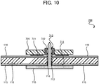
- the tack 710 described in Embodiment 1 when the tack 710 described in Embodiment 1 is inserted into the fiber structure 110, there is a possibility that the tack 710 may contact the conductive layer 116, and a short may occur between the conductive layer 115 and the conductive layer 116.
- a portion of the tack 710 is covered by an insulator 713.
- the insulator 713 contacts the conductive layer 116 and prevents the tack 710 from contacting the conductive layer 116.
- Embodiment 1 an example is described in which data is sent from the communication device 300 to the communication device 400, and data is not sent from the communication device 400 to the communication device 300.
- the communication target device 500 is a sensor instead of an actuator
- the communication device 300 is provided with a demodulation function
- the communication device 400 is provided with a modulation function.
- the communication device 300 includes a demodulation circuit 340.
- the functions of the demodulation circuit 340 are basically the same as the functions of the demodulation circuit 440. That is, the demodulation circuit 340 includes a buffer amplifier 341 that has high input impedance and is connected to a transmission path including the conductive layer 111 and the conductive layer 112. The demodulation circuit 340 is connected to the transmission path via this buffer amplifier 341. Additionally, the communication device 400 includes a modulation circuit 430, an oscillation circuit 461, an oscillation circuit 462, a bandpass filter 471, and a bandpass filter 472.
- the features of the modulation circuit 430, the features of the oscillation circuit 461, the features of the oscillation circuit 462, the features of the bandpass filter 471, and the features of the bandpass filter 472 are, respectively, basically the same as the features of the modulation circuit 330, the features of the oscillation circuit 361, the features of the oscillation circuit 362, the features of the bandpass filter 371, and the features of the bandpass filter 372.
- the modulation circuit 430 includes a switch 431, a switch 432, and a switch control circuit 433.
- the communication device 400 can send data to the communication device 300. Additionally, the communication device 400 can send an ACK to the communication device 300. Moreover, the communication device 400 can notify the communication device 300 of the busy state.
- Embodiment 3 an example is described in which the communication device 400 is provided with the oscillation circuit 462 and the like so that the communication device 400 can send not only the first data signal, but also the first clock signal. However, it is sufficient that the communication device 300 that is the master sends the first clock signal, and the communication device 400 that is a slave need not send the first clock signal.
- the communication device 400 need not include the oscillation circuit 461 and the bandpass filter 471. Additionally, the demodulation circuit 340 need not have a function for demodulating the SCL. Moreover, the modulation circuit 430 need not include the switch 431.
- the communication device 400 cannot notify the communication device 300 of the busy state, the communication device 400 can send data to the communication device 300.
- any part of the configurations, functions, and operations described in the embodiments described above may be adopted as desired. Additionally, in the present disclosure, an additional configuration, function, or operation may be adopted apart from the configurations, functions, and operations described above. Furthermore, the embodiments described above may be combined as desired. Moreover, the numbers of the constituents in the embodiments described above can be adjusted, as appropriate. Additionally, the materials, sizes, electrical characteristics, and the like usable in the present disclosure are not limited to those mentioned in the embodiments described above.
- the communication target device 500 may be a light emitting device that includes an LED or the like.
- Embodiment 1 an example is described in which ON-OFF modulation is used as the digital modulation.
- Various types of digital modulation other than ON-OFF modulation can be used. Examples thereof include amplitude shift keying (ASK) modulation, frequency shift keying (FSK) modulation, phase shift keying (PSK) modulation, and the like.
- ASK amplitude shift keying
- FSK frequency shift keying
- PSK phase shift keying
- the fiber structure 110 to which the present disclosure is applied is not limited to the fiber structure 110 of the clothing article 100.
- a configuration is possible in which the present disclosure is applied to a fiber structure 110 provided on a seat or a bed in a vehicle or facility.
- the vehicle include cars, trains, airplanes, and the like.
- Examples of the facility include entertainment facilities, schools, hospitals, and the like.
- a configuration is possible in which the present disclosure is applied to a fiber structure 110 provided on a piece of furniture or medical equipment.
- a configuration is possible in which, instead of the fiber structure 110, the present disclosure is applied to a structure that is constituted from a material other than fiber and that includes a plurality of conductive layers. Additionally, a configuration is possible in which the present disclosure is applied to a plurality of conductors that are not arranged in a laminated form. For example, the present disclosure may be applied to two electrical wires.
- Embodiment 1 is based on a premise of the functions of the communication devices 300, 400 being realized by software (or firmware), that is, a premise of many of the functions of the communication devices 300, 400 being realized by a processor executing a program.
- the communication devices 300, 400 include processing circuits instead of processors, for example.
- processing circuits are constituted by a single circuit, a composite circuit, a programmed processor, a parallel programmed processor, an application specific integrated circuit (ASIC), a field programmable gate array (FPGA), or a combination thereof.
- An operation program defining the operations of the communication devices 300, 400 according to the present disclosure can be applied to an existing personal computer, information terminal device, or the like to cause that personal computer or the like to function as the communication devices 300, 400 according to the present disclosure. Any distribution method of such a program can be used.
- the program may be stored and distributed on a non-transitory computer-readable recording medium such as a compact disc read-only memory (CD-ROM), a digital versatile disk (DVD), or a memory card, or may be distributed via a communication network (for example, the internet).
Landscapes
- Engineering & Computer Science (AREA)
- Computer Networks & Wireless Communication (AREA)
- Signal Processing (AREA)
- Theoretical Computer Science (AREA)
- Physics & Mathematics (AREA)
- General Physics & Mathematics (AREA)
- General Engineering & Computer Science (AREA)
- Electromagnetism (AREA)
- Power Engineering (AREA)
- Near-Field Transmission Systems (AREA)
- Cable Transmission Systems, Equalization Of Radio And Reduction Of Echo (AREA)
- Arrangements For Transmission Of Measured Signals (AREA)
- Textile Engineering (AREA)
Abstract
Description
- The present disclosure relates to a communication system.
- Technologies are known in which sensors, actuators, and the like are attached to a clothing article to be worn by a human to collect information about the human body, apply vibrations to the human body, and the like. In some cases, a fiber structure is used in such a clothing article. This fiber structure supplies power to the sensors, actuators, and the like, and transmits information sent or received by the sensors, the actuators, and the like. In one example, the fiber structure is formed by knitting or weaving in conductive thread having electrical conductivity and non-conductive thread not having electrical conductivity.
Patent Literature 1 discloses an example of such a fiber structure. - At least two mutually insulated conductors are required to realize the transmission of power and information. Accordingly, the fiber structure must include at least two mutually insulated conductive layers. One method for realizing communication among a plurality of communication devices using a simple configuration is a method that adopts serial communication using clock signals and data signals.
- Patent Literature 1: Unexamined
Japanese Patent Application Publication No. 2017-25432 - However, when there are only two conductors that can be used for communication, serial communication using clock signals and data signals cannot be readily adopted. In many cases, it is difficult to increase the number of conductive layers in order to realize such serial communication.
Patent Literature 1 makes no mention of a method for realizing such serial communication using two conductors. Therefore, technology for realizing, using two conductors, serial communication using clock signals and data signals is desired. - The present disclosure is made with the view of the above situation, and an objective of the present disclosure is to provide a communication system that realizes, using two conductors, serial communication using clock signals and data signals.
- A communication system according to the present disclosure that achieves the objective described above is
- a communication system including a plurality of communication devices that communicate via a first conductor and a second conductor, and a DC power supply that supplies DC power to the plurality of communication devices via the first conductor and the second conductor, wherein
- a first communication device of the plurality of communication devices including:
- a signal generation circuit that generates a clock signal that is a digital signal corresponding to a serial clock, and a data signal that is a digital signal corresponding to serial data to be sent,
- a first oscillation circuit that generates a first carrier wave having a first frequency,
- a second oscillation circuit that generates a second carrier wave having a second frequency different than the first frequency, and
- a modulation circuit that generates a first modulated signal obtained by digital modulating the first carrier wave with the clock signal and second modulated signal obtained by modulating the second carrier wave with the data signal, and applies the first modulated signal and the second modulated signal between the first conductor and the second conductor, and
- a second communication device different from the first communication device of the plurality of communication devices that is different from the first communication device, the second communication device including
- a demodulation circuit that includes a buffer amplifier that has high input impedance and that is connected to the first conductor and the second conductor, demodulates the first modulated signal and the second modulated signal applied between the first conductor and the second conductor, and generates the clock signal and the data signal, and
- a data acquisition circuit that acquires the serial data on the basis of the clock signal and the data signal generated by the demodulation circuit.
- The communication system may further include a fiber structure including a first conductive layer that has conductivity and that includes the first conductor, a second conductive layer that has conductivity and that includes the second conductor, and an insulation layer that insulates the first conductive layer and the second conductive layer.
- The communication system may further include a clothing article including the fiber structure.
- A first wavelength that is a wavelength of the first carrier wave and a second wavelength that is a wavelength of the second carrier wave may be longer than a length between two points that are separated farthest from each other on the fiber structure.
- The communication system may further include a filter circuit that is provided parallel to a capacitor including the first conductive layer and the second conductive layer, and that increases a parallel combined impedance between both ends of the capacitor at the first frequency and the second frequency.
- The communication system may further include an integration module that includes a third communication device of the plurality of communication devices, a communication target device that communicates with the third communication device, the communication target device being one selected from an actuator, a light emitting device, and a sensor, a circuit board on which the third communication device and the communication target device are mounted, and an attachment member for attaching the circuit board to the fiber structure, wherein
- the attachment member includes
- a tack constituted by a conductor, the tack being inserted into the fiber structure from a side of the first conductor toward a side of the second conductor, and
- a fixed member fixed to a protrusion of the tack on the side of the second conductor,
- the tack includes a first electrode that contacts the first conductive layer,
- the fixed member includes a second electrode that contacts the second conductive layer, and a socket into which the protrusion of the tack is inserted, and
- the circuit board is connected to the first conductive layer via the first electrode and possible in which the and is connected to the second conductive layer via the second electrode.
- A mesh-like opening may be formed in the second conductive layer, and
the tack may be inserted into the fiber structure so as to penetrate the opening and be insulated from the second conductive layer. - A portion of the tack may be covered with an insulator, and
the insulator may contact the second conductive layer, and the tack may be insulated from the second conductive layer. - According to the present disclosure, serial communication using clock signals and data signals can be realized using two conductors.
-
-
FIG. 1 is a configuration drawing of a clothing article according toEmbodiment 1 of the present disclosure; -
FIG. 2 is a disassembled perspective view of a fiber structure according toEmbodiment 1 of the present disclosure; -
FIG. 3 is a perspective view of an integration module according toEmbodiment 1 of the present disclosure; -
FIG. 4 is a cross-sectional view of an attachment member according toEmbodiment 1 of the present disclosure; -
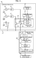
FIG. 5 is a configuration drawing of a communication system according toEmbodiment 1 of the present disclosure; -
FIG. 6 is a drawing illustrating the manner in which a clock signal changes; -
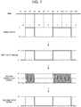
FIG. 7 is a drawing illustrating the manner in which a data signal changes; -
FIG. 8 is a circuit diagram of a communication circuit including a filter circuit provided in parallel with a capacitor; -
FIG. 9 is a drawing illustrating the relationship between the frequency of a carrier wave and the impedance between both ends of the capacitor; -
FIG. 10 is a cross-sectional view of an attachment member according to Embodiment 2 of the present disclosure; -
FIG. 11 is a configuration drawing of a communication system according toEmbodiment 3 of the present disclosure; and -
FIG. 12 is a configuration drawing of a communication system according to Embodiment 4 of the present disclosure. - Hereinafter, embodiments of the present disclosure are described while referencing the drawings. Note that, in the drawings, identical or corresponding components are denoted with the same reference numerals.
- Firstly, a
clothing article 100 according to some embodiments of the present disclosure is described while referencingFIG. 1 . Note that theclothing article 100 is a part of acommunication system 1000 according to some embodiments of the present disclosure. Theclothing article 100 is used to apply vibrations to a human body, collect information about the human body, and the like. In the present embodiment, theclothing article 100 is used to apply vibrations to a human body. In the present embodiment, theclothing article 100 is a garment. However, theclothing article 100 may be a hat, gloves, a supporter, shoes, or the like. - As illustrated in
FIG. 1 , theclothing article 100 includes afiber structure 110. Thefiber structure 110 is a structure that is constituted by fiber. Thefiber structure 110 is a wearable transmission sheet that supplies power, transmits information, and the like. Thefiber structure 110 may be used as the material of theclothing article 100, or may be attached to an existingclothing article 100 and used.FIG. 1 illustrates an example in which thefiber structure 110 is provided on only one side of the front surface of theclothing article 100. However, thefiber structure 110 may, of course, be provided at a plurality of locations of theclothing article 100. - As illustrated in
FIG. 2 , thefiber structure 110 is basically formed by laminating aconductive layer 111, aninsulation layer 113, and aconductive layer 112 in this order. Theconductive layer 111 and theconductive layer 112 include conductors and are electrically conductive layers. Theconductive layer 111 and theconductive layer 112 function as media that transmit power and information. In the present embodiment, theconductive layer 111 and theconductive layer 112 include mesh-like openings and, when viewed planarly, theconductive layer 111 and theconductive layer 112 have a lattice pattern. Note that the size of the openings, the interval of the openings, the pattern, and the like are appropriate adjusted in accordance with the application of thefiber structure 110, the power supply voltage, the signal voltage, the frequency of the signal, the maximum transmission distance, and the like. In the present embodiment, theconductive layer 112 is set to the ground potential, and power supply voltage for supplying power and signals for transmitting information are applied to theconductive layer 111. In one example, theconductive layer 111 and theconductive layer 112 are constituted from conductive thread that has electrical conductivity. However, theconductive layer 111 and theconductive layer 112 may, for example, may be formed by printing conductive ink or plating metal on a fabric constituted from non-conductive thread that does not have electrical conductivity. - The conductive thread is a thread that includes a conductor. In one example, the conductor is a substance that has a specific resistance (also called "volume resistivity") of less than 108 Ω·cm. The conductive thread may be a metal fiber constituted from a metal such as copper, stainless steel, or the like, or may be a carbon fiber constituted from carbon. Additionally, the conductive thread may be a thread that is obtained by coating a synthetic fiber with a metal by sputtering or plating. Alternatively, the conductive thread may be a thread that is obtained by kneading a conductive substance such as metal powder, conductive polymer, or the like into a synthetic fiber. Meanwhile, the non-conductive thread is a thread that does not include a conductor. For example, the non-conductive thread is a natural fiber, a synthetic fiber, a semi-synthetic fiber, an inorganic fiber, or the like.
- The
insulation layer 113 functions as a layer for insulating theconductive layer 111 and theconductive layer 112 from each other. Accordingly, theinsulation layer 113 is disposed between theconductive layer 111 and theconductive layer 112. Here, it is undesirable that theconductive layer 111 and theconductive layer 112 contact each other because, in such a case, not only will it become unable to supply power, transmit information, or the like, but a large current may flow and heat may be generated. As such, in the present embodiment, a thickness of theinsulation layer 113 is made thick enough so that theconductive layer 111 and theconductive layer 112 do not contact each other. In one example, theinsulation layer 113 is constituted from the non-conductive thread that does not have electrical conductivity. - The
conductive layer 111, theconductive layer 112, and theinsulation layer 113 may be integrally formed by knitting or weaving, or may be formed separately and fixed to each other. Examples of fixing methods include sewing using non-conductive thread, adhesion using an adhesive, affixing using double-sided tape, and the like. Thefiber structure 110 is basically constituted from the conductive thread and the non-conductive thread and, as such, is very flexible. - A plurality of
integration modules 200 is attached to thefiber structure 110. As described later, theintegration module 200 is a module that integrates devices, boards, members, and the like. Hereinafter, the configuration of theintegration module 200 is described while referencingFIG. 3 . As illustrated inFIG. 3 , theintegration module 200 includes acommunication device 400, acommunication target device 500, acircuit board 600, arelay board 610, asupport member 620, and anattachment member 700. - The
communication device 400 communicates with acommunication device 300 that is described later, and communicates with thecommunication target device 500. In the present embodiment, thecommunication device 300 and thecommunication device 400 include a half-duplex serial bus interface corresponding to an inter integrated circuit (I2C), and I2C communication is possible. I2C communication is a communication system in which one master communicates with one or more slaves using a serial clock (SCL) that is a serial clock line and serial data (SDA) that is a serial data line. In the present embodiment, thecommunication device 300 is the master, and thecommunication device 400 is a slave. - The SCL is a signal line used for synchronization. The SDA is a signal line that is synchronized with the SCL, and is used to transmit data. In the present embodiment, the state of the SCL and the state of the SDA are controlled by the master. The SCL and the SDA are set by the master to H-level (power supply potential, namely Vcc) or L-level (ground potential, namely 0 V). Note that, in typical I2C communication, when a slave notifies a busy state, the state of the SCL is sometimes controlled by the slave, but this feature is not used in the present embodiment. Additionally, in typical I2C communication, when a slave sends data or sends an ACK, the state of the SCL is sometimes controlled by the slave, but this feature is not used in the present embodiment. Moreover, in typical I2C communication, both the SCL and the SDA are open collector connections or open drain connections, and the signal line is pulled up to the power supply voltage via a resistor. However, in the present embodiment, for example, an output terminal of the SCL and an output terminal of the SDA are pulled up to the power supply voltage via a resistor in a
switch control circuit 333, and are output as H-level or L-level voltage. - Typically, in I2C communication, the master and the slaves are connected to each other by the SCL, the SDA, and the ground line. However, in the present embodiment, the
communication device 300 and thecommunication device 400 are connected to each other by theconductive layer 111 and theconductive layer 112. Here, theconductive layer 112 fulfills a role as the ground line. As such, in the present embodiment, both the data to be sent using the SCL and the data to be sent using the SDA must be sent using theconductive layer 111. Therefore, in the present embodiment, a system is adopted in which two carrier waves having different frequencies are each modulated with two pieces of data, and the two modulated signals obtained by the modulating are superimposed on theconductive layer 111. - In the present embodiment, the
communication target device 500 is an actuator. Accordingly, it is sufficient that thecommunication device 400 controls thecommunication target device 500 on the basis of data received from thecommunication device 300. Therefore, thecommunication device 400 does not need to receive data from thecommunication target device 500 and send the received data to thecommunication device 300. As such, thecommunication device 400 includes a function for receiving data from thecommunication device 300, but does not include a function for sending data to thecommunication device 300. Note that thecommunication device 400 does not include a function for sending an ACK to thecommunication device 300 and a function for notifying a busy state, and it is sufficient that thecommunication device 300 not use these functions. As described above, thecommunication device 400 controls thecommunication target device 500 on the basis of data received from thecommunication device 300. - The
communication target device 500 is a communication target of thecommunication device 400, and is controlled by thecommunication device 400. As described above, in the present embodiment, thecommunication target device 500 is an actuator. Accordingly, thecommunication target device 500 vibrates in accordance with commands from thecommunication device 400, and applies vibration to the human body of the wearer of theclothing article 100. - The
circuit board 600 is a circuit board on which thecommunication device 400 and thecommunication target device 500 are mounted. Thecircuit board 600 includes anelectrode 601 and anelectrode 602. Theelectrode 601 is connected to theconductive layer 111 via anelectrical wire 603. Theelectrode 602 is connected to theconductive layer 112 via anelectrical wire 604. Thecircuit board 600 supplies DC power to thecommunication device 400 and thecommunication target device 500 via theelectrode 601 and theelectrode 602. Additionally, thecircuit board 600 supplies signals to thecommunication device 400 via theelectrode 601 and theelectrode 602. - The
relay board 610 relays the connection between theconductive layer 111 and theelectrode 601 and the connection between theconductive layer 112 and theelectrode 602. Therelay board 610 supports theattachment member 700 described later and also is fixed to thecircuit board 600 by theelectrical wire 603, theelectrical wire 604, and anelectrical wire 605. Therelay board 610 connects theconductive layer 111 to theelectrode 601 by connecting asocket 722 described later to theelectrical wire 603. Additionally, therelay board 610 connects theconductive layer 112 to theelectrode 602 by connecting anelectrode 721 described later to theelectrical wire 604. - The
support member 620 is a member that supports thecircuit board 600, and serves as a base of theentire integration module 200. Theattachment member 700 is a member for attaching theintegration module 200 to thefiber structure 110. Theattachment member 700 includes atack 710 and a fixedmember 720. - The
tack 710 is a member that is inserted into thefiber structure 110 from a first conductive layer side toward a second conductive layer side. In one example, the first conductive layer is theconductive layer 111. In one example, the second conductive layer is theconductive layer 112. However, the first conductive layer may be theconductive layer 112 and the second conductive layer may be theconductive layer 111. Thetack 710 is constituted by a conductor. Thetack 710 includes a first electrode and aprotrusion 712. The first electrode is a portion that contacts the first conductive layer when thetack 710 is inserted into thefiber structure 110. In one example, the first electrode is anelectrode 711. Theelectrode 711 is a portion of back surface of the umbrella-like part of thetack 710. Theprotrusion 712 is a portion that protrudes from the second conductive layer when thetack 710 is inserted into thefiber structure 110. - The fixed
member 720 fixes to theprotrusion 712 of thetack 710 on the second conductor layer side. The fixedmember 720 includes a second electrode and asocket 722. The second electrode contacts the second conductive layer. In one example, the second electrode is anelectrode 721. Theelectrode 721 is constituted by a conductor. Theprotrusion 712 of thetack 710 is inserted into thesocket 722. Thesocket 722 is constituted by a conductor. -
FIG. 4 illustrates a situation in which thetack 710 inserted into thefiber structure 110 is fixed by the fixedmember 720, and theintegration module 200 is fixed to thefiber structure 110.FIG. 4 is a cross-sectional view of thetack 710 and thefiber structure 110, taken along a cross-section including a center axis of theprotrusion 712 of thetack 710. - Firstly, the
tack 710 is inserted into thefiber structure 110 so as to pass through an opening of theconductive layer 112 from theconductive layer 111 side toward theconductive layer 112 side. Specifically, thetack 710 is inserted into thefiber structure 110 from theconductive layer 111 side so as to avoid theconductive layer 112. As the insertion of thetack 710 progresses, thetack 710 penetrates thefiber structure 110, and theprotrusion 712 of thetack 710 protrudes to theconductive layer 112 side. Then, when the insertion of thetack 710 progresses from here, theelectrode 711 of thetack 710 contacts theconductive layer 111, and further insertion of thetack 710 is prevented. - Here, the fixed
member 720 is pressed against thefiber structure 110 from theconductive layer 112 side such that theprotrusion 712 of thetack 710 is inserted into thesocket 722 of the fixedmember 720. Then, theprotrusion 712 of thetack 710 is inserted into thesocket 722 of the fixedmember 720. At this time, theprotrusion 712 contacts thesocket 722, and thetack 710 is supported by the fixedmember 720. Here, when the fixedmember 720 is further pressed against thefiber structure 110, theelectrode 721 of the fixedmember 720 contacts theconductive layer 112, and movement of the fixedmember 720 is suppressed. - Thus, when the
protrusion 712 that penetrates thefiber structure 110 is fitted into thesocket 722, thetack 710 and the fixedmember 720 are fixed to each other in a state in which thetack 710 and the fixedmember 720 sandwich thefiber structure 110. When thetack 710 and the fixedmember 720 are fixed, theattachment member 700 is fixed to thefiber structure 110 and, as a result, theintegration module 200 is fixed to thefiber structure 110. - At this time, the
electrode 711 contacts theconductive layer 111, and theprotrusion 712 contacts thesocket 722. Here, thesocket 722 is connected to theelectrode 601 via therelay board 610 and theelectrical wire 603. That is, thecircuit board 600 is connected to theconductive layer 111 via theelectrode 711 and thesocket 722. Additionally, theelectrode 721 contacts theconductive layer 112. Moreover, theelectrode 721 is connected to theelectrode 602 via therelay board 610 and theelectrical wire 604. That is, thecircuit board 600 is connected to theconductive layer 112 via theelectrode 721. - An example in which the
integration module 200 includes thecommunication device 400 is described above. The attaching of theintegration module 200 to thefiber structure 110 is the same when theintegration module 200 includes thecommunication device 300 and also when theintegration module 200 includes aDC power supply 380. Note that, when theintegration module 200 includes thecommunication device 300, theintegration module 200 includes thecommunication device 300 instead of thecommunication device 400, and does not include thecommunication target device 500. Additionally, when theintegration module 200 includes theDC power supply 380, theintegration module 200 includes theDC power supply 380 instead of thecommunication device 400 and thecommunication target device 500. In the present embodiment, theintegration module 200 includes thecommunication device 300 and theDC power supply 380. - Next, a detailed description of the configuration of the
communication system 1000 is given while referencingFIG. 5 . As illustrated inFIG. 5 , thecommunication system 1000 includes at least thecommunication device 300, thecommunication device 400, thecommunication target device 500, and theconductive layer 111. Thecommunication device 300 functions as the master, and thecommunication device 400 functions as a slave. In one example, a first communication device corresponds to thecommunication device 300. In one example, a second communication device corresponds to thecommunication device 400. Note that, in the present embodiment, both thecommunication device 300 and thecommunication device 400 are a third communication device and are organized together with thecircuit board 600 and theattachment member 700 as theintegration module 200. Thecommunication target device 500 is controlled by thecommunication device 300 via thecommunication device 400. A modulated signal corresponding to the SCL and a modulated signal corresponding to the SDA are superimposed on theconductive layer 111. - The
communication device 300 includes acontrol circuit 310, acommunication circuit 320, amodulation circuit 330, anoscillation circuit 361, anoscillation circuit 362, abandpass filter 371, abandpass filter 372, theDC power supply 380, and aninductor 381. - The
control circuit 310 controls the operations of theentire communication device 300. For example, thecontrol circuit 310 supplies serial data to thecommunication circuit 320. This serial data is serial data to be sent and, specifically, is serial data to be sent to thecommunication device 400 in order to control thecommunication target device 500. - The
communication circuit 320 is a communication circuit for realizing I2C communication. Thecommunication circuit 320 generates a first clock signal and a first data signal. That is, thecommunication circuit 320 is a signal generation circuit. The first clock signal is a digital signal corresponding to a serial clock. The first data signal is a digital signal corresponding to serial data to be sent. Note that, in one example, the first clock signal is a signal that alternately demonstrates an H-level representing the power supply potential (Vcc) and an L-level representing the ground potential (0 V). Additionally, in one example the first data signal is a signal that demonstrates the H-level representing the power supply potential (Vcc) when the serial data is 1, and demonstrates the L-level representing the ground potential (0 V) when the serial data is 0. - The
modulation circuit 330 generates the first modulated signal and the second modulated signal, and applies the first modulated signal and the second modulated signal between the first conductive layer and the second conductive layer. The first modulated signal is a signal that is obtained by ON-OFF modulating a first carrier wave with the first clock signal. The first carrier wave is a carrier wave that has a first frequency. The first carrier wave is generated by a first oscillation circuit. In one example, the first oscillation circuit is theoscillation circuit 361. The second modulated signal is a signal that is obtained by ON-OFF modulating a second carrier wave with the first data signal. The second carrier wave is a carrier wave that has a second frequency different from the first frequency. The second carrier wave is generated by a second oscillation circuit. In one example, the second oscillation circuit is theoscillation circuit 362. - The
modulation circuit 330 includes aswitch 331, aswitch 332, and aswitch control circuit 333. Theswitch 331 is a switch for controlling conduction and interruption to theconductive layer 111 of the first carrier wave generated by theoscillation circuit 361. Theswitch 332 is a switch for controlling conduction and interruption to theconductive layer 111 of the second carrier wave generated by theoscillation circuit 362. Theswitch control circuit 333 is a circuit that controls the state of theswitch 331 and the state of theswitch 332. In one example, theswitch control circuit 333 controls theswitch 331 to an interrupted state when the first clock signal is the L-level, and controls theswitch 331 to a conduction state with the first clock signal is the H-level. In one example, theswitch control circuit 333 controls theswitch 332 to the interrupted state when the first data signal is the L-level, and controls theswitch 332 to the conduction state with the first data signal is the H-level. - The
oscillation circuit 361 is a circuit that generates the first carrier wave that has the first frequency. Theoscillation circuit 362 is a circuit that generates the second carrier wave that has the second frequency. In the present embodiment, the first frequency is 5 MHz, and the second frequency is 2 MHz Additionally, the clock frequency of the I2C communication, that is, the frequency of the first clock signal, is 10 kHz. - The
bandpass filter 371 is a filter that allows signals that have the first frequency to pass, and that blocks signals that have frequencies other than the first frequency. Specifically, thebandpass filter 371 is a filter that allows the first carrier wave to pass, and that blocks the passage of the second carrier wave, harmonics of the first carrier wave and the second carrier wave, and the like. Thebandpass filter 372 is a filter that allows signals that have the second frequency to pass, and that blocks signals that have frequencies other than the second frequency. Specifically, thebandpass filter 372 is a filter that allows the second carrier wave to pass, and that blocks the passage of the first carrier wave, harmonics of the first carrier wave and the second carrier wave, and the like. - Next, the configuration of the
communication device 400 is described. Thecommunication device 400 includes acontrol circuit 410, acommunication circuit 420, ademodulation circuit 440, and asecond communication circuit 450. - The
control circuit 410 controls the operations of theentire communication device 400. In one example, thecontrol circuit 410 controls thecommunication target device 500 via thesecond communication circuit 450 on the basis of the serial data supplied from thecommunication circuit 420. - The
communication circuit 420 is a communication circuit for realizing I2C communication. Thecommunication circuit 420 acquires the serial data on the basis of a second clock signal and a second data signal generated by thedemodulation circuit 440. In other words, thecommunication circuit 420 is a data acquisition circuit. - The
demodulation circuit 440 includes abuffer amplifier 441 that has high input impedance and that is connected to a transmission path including theconductive layer 111 and theconductive layer 112. Thedemodulation circuit 440 is connected to the transmission path via thisbuffer amplifier 441. It is preferable that the input impedance of thebuffer amplifier 441 is sufficiently higher than the output impedance of theoscillation circuit 361 and the output impedance of theoscillation circuit 362. In this case, it is possible to receive the first modulated signal and the second modulated signal, even if a plurality ofbuffer amplifiers 441 is connected in parallel to the transmission path. That is, in the present embodiment, each individual input impedance of thedemodulation circuit 440 of thecommunication device 400 connected to the transmission path is high and, as such, normal communication operations can be realized even ifmultiple communication devices 400 are connected in parallel to the transmission path. - Here, the
demodulation circuit 440 demodulates the first modulated signal that is applied between theconductive layer 111 of the first conductor and theconductive layer 112 of the second conductor, and generates the second clock signal. In one example, thedemodulation circuit 440 acquires, via a bandpass filter similar to thebandpass filter 371, the first modulated signal applied between theconductive layer 111 and theconductive layer 112. Then, thedemodulation circuit 440 determines whether the first modulated signal has amplitude, and generates the second clock signal. The second clock signal is basically a signal similar to the first clock signal, and is a digital signal corresponding to the serial clock. Note that, in one example, the second clock signal is a signal that is the L-level when the first modulated signal does not have amplitude, and is the H-level when the first modulated signal has amplitude. That is, the second clock signal is a signal that is the H-level when the first clock signal is the H-level, and is the L-level when the first clock signal is the L-level. - The
demodulation circuit 440 demodulates the second modulated signal applied between theconductive layer 111 and theconductive layer 112, and generates the second data signal. In one example, thedemodulation circuit 440 acquires, via a bandpass filter similar to thebandpass filter 372, the second modulated signal applied between theconductive layer 111 and theconductive layer 112. Then, thedemodulation circuit 440 determines whether the second modulated signal has amplitude, and generates the second data signal. The second data signal is basically a signal similar to the first data signal, and is a digital signal corresponding to the serial data. Note that, in one example, the second data signal is a signal that is the L-level when the second modulated signal does not have amplitude, and is the H-level when the second modulated signal has amplitude. That is, the second data signal is a signal that is the H-level when the first data signal is the H-level, and is the L-level when the first data signal is the L-level. - The
second communication circuit 450 is a communication circuit for enabling thecommunication device 400 to communicate with thecommunication target device 500. Thesecond communication circuit 450 sends, in accordance with control by thecontrol circuit 410, information for controlling thecommunication target device 500 to thecommunication target device 500. Thecommunication target device 500 operates in accordance with the information received from thesecond communication circuit 450. - Next, the manner in which the clock signal changes is described while referencing
FIG. 6 . Firstly, thecommunication circuit 320 generates the first clock signal that is a digital signal corresponding to the serial clock. This first clock signal is converted to the first modulated signal by themodulation circuit 330. The first modulated signal superimposed between theconductive layer 111 and theconductive layer 112 is converted to the second clock signal by thedemodulation circuit 440. This second clock signal is used when thecommunication circuit 420 acquires the serial data from the second data signal. - Here, in one example, when the first clock signal is the H-level, the first modulated signal has amplitude and the second clock signal is the H-level. Meanwhile, in one example, when the first clock signal is the L-level, the first modulated signal does not have amplitude and the second clock signal is the L-level.
- Next, the manner in which the data signal changes is described while referencing
FIG. 7 . This serial data is converted to the first data signal by thecommunication circuit 320. This first data signal is converted to the second modulated signal by themodulation circuit 330. The second modulated signal superimposed between theconductive layer 111 and theconductive layer 112 is converted to the second data signal by thedemodulation circuit 440. This second data signal is converted to serial data by thecommunication circuit 420. - Here, in one example, when the serial data is 1, the first data signal is the H-level, the second modulated signal has amplitude, and the second data signal is the H-level. Meanwhile, in one example, when the serial data is 0, the first data signal is the L-level, the second modulated signal does not have amplitude, and the second data signal is the L-level.
- Next, descriptions are given of the first frequency and the second frequency. The first modulated signal that has the first frequency and the second modulated signal that has the second frequency are simultaneously applied between the
conductive layer 111 and theconductive layer 112. Accordingly, it is preferable that the difference between the first frequency and the second frequency is greater than or equal to a threshold. In one example, this threshold is determined in consideration of the performance of the bandpass filter, the perspective of EMC, and the like. - The first carrier wave that has the first frequency is ON-OFF modulated by the first clock signal, and the second carrier wave that has the second frequency is ON-OFF modulated by the first data signal. Accordingly, the first frequency must be sufficiently higher than the frequency of the first clock signal. Likewise, the second frequency must be sufficiently higher than the frequency of the first data signal. As such, it is preferable to increase the first frequency and the second frequency to increase the communication speed of the I2C communication.
- However, the wavelength of the first modulated signal that has the first frequency shortens as the first frequency increases. Moreover, in a case in which the wavelength of the first modulated signal is shorter than the length between two points separated the farthest from each other on the
fiber structure 110, a standing wave is generated on thefiber structure 110. If a standing wave is generated on thefiber structure 110, locations develop where the first modulated signal attenuates, and the possibility of thecommunication device 300 and thecommunication device 400 not being able to normally communicate increases. Accordingly, it is preferable that the wavelength of the first modulated signal is sufficiently long with respect to the length of thefiber structure 110. Note that the wavelength of the first modulated signal is basically the wavelength of the first modulated signal when the first modulated signal propagates through thefiber structure 110, and is shorter than the wavelength in vacuum of the first modulated signal. The same is true for the wavelength of the second modulated signal. - As the capacitance between the
conductive layer 111 and theconductive layer 112 increases or, as the first frequency increases, the impedance between theconductive layer 111 and theconductive layer 112 decreases, and the first modulated signal attenuates. The same is true for the second modulated signal. Here, it may not be possible to significantly reduce the capacitance between theconductive layer 111 and theconductive layer 112 due to various restrictions. Additionally, it may not be possible to significantly lower the first frequency due to restrictions such as communication speed and the like. - In such a case, as illustrated in
FIG. 8 , it is preferable to provide afilter circuit 373 in parallel with acapacitor 114 constituted by theconductive layer 111 and theconductive layer 112, and increase the parallel combined impedance at the first frequency and the second frequency of aparallel circuit 374 including thecapacitor 114 and thefilter circuit 373. Such a configuration is expected to result in an increase in the gain at the first frequency and the second frequency, and a decrease in the attenuation rates of the first modulated signal and the second modulated signal. Note thatFIG. 8 illustrates an example in which theoscillation circuit 361 is divided into anideal oscillation circuit 363 that does not include aninternal resistor 364 and theinternal resistor 364, and theoscillation circuit 362 is divided into and anideal oscillation circuit 365 that does not include aninternal resistor 366 and theinternal resistor 366. Thefilter circuit 373 is a circuit that includes a plurality of inductors and a plurality of capacitors, for example. -
FIG. 9 illustrates the relationship between the frequency of the signal and the parallel combined impedance of theparallel circuit 374. As illustrated inFIG. 9 , basically, the parallel combined impedance of theparallel circuit 374 decreases as the frequency of the signal increases. However,FIG. 9 also illustrates that the parallel combined impedance relatively increases at the first frequency and the second frequency due to the selection of thefilter circuit 373. - According to the present embodiment, it is possible to carry out serial communication, by appropriately using clock signals and data signals, among a plurality of communication devices, by using the two conductive layers of the
fiber structure 110. - In
Embodiment 1, an example is described in which aconductive layer 111 in which mesh-like openings are formed is used as the first conductive layer, and aconductive layer 112 in which mesh-like openings are formed is used as the second conductive layer. As illustrated inFIG. 10 , a configuration is possible in which aconductive layer 115 that does not include openings is used as the first conductive layer, and aconductive layer 116 that does not include openings is used as the second conductive layer. - With such a configuration, when the
tack 710 described inEmbodiment 1 is inserted into thefiber structure 110, there is a possibility that thetack 710 may contact theconductive layer 116, and a short may occur between theconductive layer 115 and theconductive layer 116. As such, in the present embodiment, as illustrated inFIG. 10 , a portion of thetack 710 is covered by aninsulator 713. In this case, theinsulator 713 contacts theconductive layer 116 and prevents thetack 710 from contacting theconductive layer 116. - In
Embodiment 1, an example is described in which data is sent from thecommunication device 300 to thecommunication device 400, and data is not sent from thecommunication device 400 to thecommunication device 300. In a case such as when thecommunication target device 500 is a sensor instead of an actuator, it may be desired to send data from thecommunication device 400 to thecommunication device 300. In such a case, it is preferable that thecommunication device 300 is provided with a demodulation function, and thecommunication device 400 is provided with a modulation function. - In one example of such a case, as illustrated in
FIG. 11 , thecommunication device 300 includes ademodulation circuit 340. The functions of thedemodulation circuit 340 are basically the same as the functions of thedemodulation circuit 440. That is, thedemodulation circuit 340 includes abuffer amplifier 341 that has high input impedance and is connected to a transmission path including theconductive layer 111 and theconductive layer 112. Thedemodulation circuit 340 is connected to the transmission path via thisbuffer amplifier 341. Additionally, thecommunication device 400 includes amodulation circuit 430, anoscillation circuit 461, anoscillation circuit 462, abandpass filter 471, and abandpass filter 472. The features of themodulation circuit 430, the features of theoscillation circuit 461, the features of theoscillation circuit 462, the features of thebandpass filter 471, and the features of thebandpass filter 472 are, respectively, basically the same as the features of themodulation circuit 330, the features of theoscillation circuit 361, the features of theoscillation circuit 362, the features of thebandpass filter 371, and the features of thebandpass filter 372. Themodulation circuit 430 includes aswitch 431, aswitch 432, and aswitch control circuit 433. - According to this configuration, the
communication device 400 can send data to thecommunication device 300. Additionally, thecommunication device 400 can send an ACK to thecommunication device 300. Moreover, thecommunication device 400 can notify thecommunication device 300 of the busy state. - In
Embodiment 3, an example is described in which thecommunication device 400 is provided with theoscillation circuit 462 and the like so that thecommunication device 400 can send not only the first data signal, but also the first clock signal. However, it is sufficient that thecommunication device 300 that is the master sends the first clock signal, and thecommunication device 400 that is a slave need not send the first clock signal. - In this case, as illustrated in
FIG. 12 , thecommunication device 400 need not include theoscillation circuit 461 and thebandpass filter 471. Additionally, thedemodulation circuit 340 need not have a function for demodulating the SCL. Moreover, themodulation circuit 430 need not include theswitch 431. - With this configuration as well, although the
communication device 400 cannot notify thecommunication device 300 of the busy state, thecommunication device 400 can send data to thecommunication device 300. - Embodiments of the present disclosure are described above. However, various modifications and applications are possible when implementing the present disclosure.
- In the present disclosure, any part of the configurations, functions, and operations described in the embodiments described above may be adopted as desired. Additionally, in the present disclosure, an additional configuration, function, or operation may be adopted apart from the configurations, functions, and operations described above. Furthermore, the embodiments described above may be combined as desired. Moreover, the numbers of the constituents in the embodiments described above can be adjusted, as appropriate. Additionally, the materials, sizes, electrical characteristics, and the like usable in the present disclosure are not limited to those mentioned in the embodiments described above.
- For example, the
communication target device 500 may be a light emitting device that includes an LED or the like. - In
Embodiment 1, an example is described in which ON-OFF modulation is used as the digital modulation. Various types of digital modulation other than ON-OFF modulation can be used. Examples thereof include amplitude shift keying (ASK) modulation, frequency shift keying (FSK) modulation, phase shift keying (PSK) modulation, and the like. - In
Embodiment 1, an example is described in which the present disclosure is applied to thefiber structure 110 of theclothing article 100. However, thefiber structure 110 to which the present disclosure is applied is not limited to thefiber structure 110 of theclothing article 100. For example, a configuration is possible in which the present disclosure is applied to afiber structure 110 provided on a seat or a bed in a vehicle or facility. Examples of the vehicle include cars, trains, airplanes, and the like. Examples of the facility include entertainment facilities, schools, hospitals, and the like. Alternatively, a configuration is possible in which the present disclosure is applied to afiber structure 110 provided on a piece of furniture or medical equipment. - A configuration is possible in which, instead of the
fiber structure 110, the present disclosure is applied to a structure that is constituted from a material other than fiber and that includes a plurality of conductive layers. Additionally, a configuration is possible in which the present disclosure is applied to a plurality of conductors that are not arranged in a laminated form. For example, the present disclosure may be applied to two electrical wires. - The description of Embodiment 1is based on a premise of the functions of the
communication devices communication devices communication devices - An operation program defining the operations of the
communication devices communication devices - The foregoing describes some example embodiments for explanatory purposes. Although the foregoing discussion has presented specific embodiments, persons skilled in the art will recognize that changes may be made in form and detail without departing from the broader spirit and scope of the invention. Accordingly, the specification and drawings are to be regarded in an illustrative rather than a restrictive sense. This detailed description, therefore, is not to be taken in a limiting sense, and the scope of the invention is defined only by the included claims, along with the full range of equivalents to which such claims are entitled.
- This application claims the benefit of
Japanese Patent Application No. 2018-159542, filed on August 28, 2018 -
- 100
- Clothing article
- 110
- Fiber structure
- 111, 112, 115, 116
- Conductive layer
- 113
- Insulation layer
- 114
- Capacitor
- 200
- Integration module
- 300, 400
- Communication device
- 310, 410
- Control circuit
- 320, 420
- Communication circuit
- 330, 430
- Modulation circuit
- 331, 332, 431, 432
- Switch
- 333,433
- Switch control circuit
- 340, 440
- Demodulation circuit
- 341, 441
- Buffer amplifier
- 361, 362, 363, 365, 461, 462
- Oscillation circuit
- 364, 366
- Internal resistor
- 371, 372, 471, 472
- Bandpass filter
- 373
- Filter circuit
- 374
- Parallel circuit
- 380
- DC power supply
- 381
- Inductor
- 450
- Second communication circuit
- 500
- Communication target device
- 600
- Circuit board
- 601, 602, 711, 721
- Electrode
- 603, 604,
- 605 Electrical wire
- 610
- Relay board
- 620
- Support member
- 700
- Attachment member
- 710
- Tack
- 712
- Protrusion
- 713
- Insulator
- 720
- Fixed member
- 722
- Socket
- 1000
- Communication system
Claims (8)
- A communication system comprising a plurality of communication devices that communicate via a first conductor and a second conductor, and a DC power supply that supplies DC power to the plurality of communication devices via the first conductor and the second conductor, whereina first communication device of the plurality of communication devices includinga signal generation circuit that generates a clock signal that is a digital signal corresponding to a serial clock, and a data signal that is a digital signal corresponding to serial data to be sent,a first oscillation circuit that generates a first carrier wave having a first frequency,a second oscillation circuit that generates a second carrier wave having a second frequency different than the first frequency, anda modulation circuit that generates a first modulated signal obtained by digital modulating the first carrier wave with the clock signal and second modulated signal obtained by modulating the second carrier wave with the data signal, and applies the first modulated signal and the second modulated signal between the first conductor and the second conductor, anda second communication device of the plurality of communication devices that is different from the first communication device, the second communication device includinga demodulation circuit that includes a buffer amplifier that has high input impedance and that is connected to the first conductor and the second conductor, demodulates the first modulated signal and the second modulated signal applied between the first conductor and the second conductor, and generates the clock signal and the data signal, anda data acquisition circuit that acquires the serial data on the basis of the clock signal and the data signal generated by the demodulation circuit.
- The communication system according to claim 1, further comprising:
a fiber structure including a first conductive layer that has conductivity and that includes the first conductor, a second conductive layer that has conductivity and that includes the second conductor, and an insulation layer that insulates the first conductive layer and the second conductive layer. - The communication system according to claim 2, further comprising:
a clothing article including the fiber structure. - The communication system according to claim 2 or 3, wherein a first wavelength that is a wavelength of the first carrier wave and a second wavelength that is a wavelength of the second carrier wave are longer than a length between two points that are separated farthest from each other on the fiber structure.
- The communication system according to any one of claims 2 to 4, further comprising:
a filter circuit that is provided parallel to a capacitor including the first conductive layer and the second conductive layer, and that increases a parallel combined impedance between both ends of the capacitor at the first frequency and the second frequency. - The communication system according to any one of claims 2 to 5, further comprising:an integration module that includes a third communication device of the plurality of communication devices, a communication target device that communicates with the third communication device, the communication target device being one selected from an actuator, a light emitting device, and a sensor, a circuit board on which the third communication device and the communication target device are mounted, and an attachment member for attaching the circuit board to the fiber structure, whereinthe attachment member includesa tack constituted by a conductor, the tack being inserted into the fiber structure from a side of the first conductive layer toward a side of the second conductive layer, anda fixed member fixed to a protrusion of the tack on the side of the second conductive layer,the tack includes a first electrode that contacts the first conductive layer,the fixed member includes a second electrode that contacts the second conductive layer, and a socket into which the protrusion of the tack is inserted, andthe circuit board is connected to the first conductive layer via the first electrode and the socket, and is connected to the second conductive layer via the second electrode.
- The communication system according to claim 6, wherein
a mesh-like opening is formed in the second conductive layer, and
the tack is inserted into the fiber structure so as to penetrate the opening, and is insulated from the second conductive layer. - The communication system according to claim 6, wherein
a portion of the tack is covered with an insulator, and
the insulator contacts the second conductive layer, and the tack is insulated from the second conductive layer.
Applications Claiming Priority (2)
| Application Number | Priority Date | Filing Date | Title |
|---|---|---|---|
| JP2018159542A JP6498827B1 (en) | 2018-08-28 | 2018-08-28 | Communications system |
| PCT/JP2018/045743 WO2020044583A1 (en) | 2018-08-28 | 2018-12-12 | Communication system |
Publications (2)
| Publication Number | Publication Date |
|---|---|
| EP3846363A1 true EP3846363A1 (en) | 2021-07-07 |
| EP3846363A4 EP3846363A4 (en) | 2022-06-01 |
Family
ID=66092677
Family Applications (1)
| Application Number | Title | Priority Date | Filing Date |
|---|---|---|---|
| EP18931521.1A Withdrawn EP3846363A4 (en) | 2018-08-28 | 2018-12-12 | Communication system |
Country Status (5)
| Country | Link |
|---|---|
| US (1) | US20210328688A1 (en) |
| EP (1) | EP3846363A4 (en) |
| JP (1) | JP6498827B1 (en) |
| CN (1) | CN112585893A (en) |
| WO (1) | WO2020044583A1 (en) |
Families Citing this family (3)
| Publication number | Priority date | Publication date | Assignee | Title |
|---|---|---|---|---|
| JP7330812B2 (en) * | 2019-08-13 | 2023-08-22 | 日清紡マイクロデバイス株式会社 | signal processing system |
| JP6653819B1 (en) * | 2019-09-09 | 2020-02-26 | 学校法人南山学園 | Wearable biological sensing system |
| JP6990953B1 (en) * | 2021-10-04 | 2022-01-12 | 学校法人南山学園 | Connector for conductive cloth |
Family Cites Families (25)
| Publication number | Priority date | Publication date | Assignee | Title |
|---|---|---|---|---|
| JPS6377290A (en) * | 1986-09-20 | 1988-04-07 | Victor Co Of Japan Ltd | Hue variable circuit |
| JP2518708B2 (en) * | 1989-12-20 | 1996-07-31 | セイコー電子工業株式会社 | Portable information device |
| WO1996031038A1 (en) * | 1995-03-24 | 1996-10-03 | Hitachi, Ltd. | Data transmitting method and transmission/reception circuit used therefor, and signal processor |
| JPH1098439A (en) * | 1996-09-20 | 1998-04-14 | Oki Electric Ind Co Ltd | Optical signal transmitter, optical signal receiver and optical signal transmitter-receiver |
| US6442179B2 (en) * | 1997-08-15 | 2002-08-27 | Seagate Technology Llc | Data storage communication channel and method of transmitting data |
| JP3862212B2 (en) * | 2001-10-29 | 2006-12-27 | 松下電器産業株式会社 | Optical transmission system and optical receiver |
| JP4012032B2 (en) * | 2001-11-20 | 2007-11-21 | キヤノン株式会社 | Data communication device |
| WO2004091108A1 (en) * | 2003-04-01 | 2004-10-21 | Nec Corporation | Information processing terminal system and transmission/reception method using the same |
| EP1636706A2 (en) * | 2003-06-13 | 2006-03-22 | International Business Machines Corporation | Serial bus interface and method for serially interconnecting time-critical digital devices |
| JP2005286774A (en) * | 2004-03-30 | 2005-10-13 | Sanyo Electric Co Ltd | Transmission signal generating device |
| JP4419082B2 (en) * | 2005-03-24 | 2010-02-24 | ヤマハ株式会社 | Communications system |
| WO2007119405A1 (en) * | 2006-04-03 | 2007-10-25 | Brother Kogyo Kabushiki Kaisha | Radio communication device |
| JP4250634B2 (en) * | 2006-04-18 | 2009-04-08 | キヤノン株式会社 | Data communication apparatus, data communication system, and data communication method |
| KR100968865B1 (en) * | 2007-12-17 | 2010-07-09 | 주식회사 애트랩 | Serial communication system and its ID method |
| US8831073B2 (en) * | 2009-08-31 | 2014-09-09 | Sony Corporation | Wireless transmission system, wireless communication device, and wireless communication method |
| JP5692093B2 (en) * | 2010-01-22 | 2015-04-01 | 日本電気株式会社 | Data communication system and method, data transmission apparatus and method, data reception apparatus and method |
| JP2011259091A (en) * | 2010-06-07 | 2011-12-22 | Sony Corp | Signal transmission system, signal processor, reference signal transmitter, reference signal receiver, electronic apparatus, signal transmission method |
| JP2012147351A (en) * | 2011-01-14 | 2012-08-02 | Sony Corp | Signal transmission device, electronic device, and signal transmission method |
| JP5644521B2 (en) * | 2011-01-14 | 2014-12-24 | ソニー株式会社 | Signal transmission device and electronic device |
| US8958497B2 (en) * | 2012-06-12 | 2015-02-17 | Silicon Image, Inc. | Simultaneous transmission of clock and bidirectional data over a communication channel |
| JP6560043B2 (en) | 2015-07-22 | 2019-08-14 | 帝人フロンティア株式会社 | Conductive warp knitted fabric and use thereof |
| CN105249943A (en) * | 2015-08-26 | 2016-01-20 | 金卫华 | An intelligent clothes control system and a control method thereof |
| US10241942B2 (en) * | 2016-06-28 | 2019-03-26 | Mediatek Inc. | Method and apparatus for memory access |
| JP6377290B1 (en) * | 2018-03-01 | 2018-08-22 | 学校法人南山学園 | Communications system |
| JP6492214B2 (en) | 2018-06-25 | 2019-03-27 | 日立アプライアンス株式会社 | Opening device and device provided with opening device |
-
2018
- 2018-08-28 JP JP2018159542A patent/JP6498827B1/en active Active
- 2018-12-12 WO PCT/JP2018/045743 patent/WO2020044583A1/en not_active Ceased
- 2018-12-12 CN CN201880096976.XA patent/CN112585893A/en active Pending
- 2018-12-12 EP EP18931521.1A patent/EP3846363A4/en not_active Withdrawn
- 2018-12-12 US US17/271,953 patent/US20210328688A1/en not_active Abandoned
Also Published As
| Publication number | Publication date |
|---|---|
| WO2020044583A1 (en) | 2020-03-05 |
| US20210328688A1 (en) | 2021-10-21 |
| JP2020036130A (en) | 2020-03-05 |
| EP3846363A4 (en) | 2022-06-01 |
| CN112585893A (en) | 2021-03-30 |
| JP6498827B1 (en) | 2019-04-10 |
Similar Documents
| Publication | Publication Date | Title |
|---|---|---|
| US20210328688A1 (en) | Communication system | |
| CN204305287U (en) | Headphone signal multiplex system | |
| JP6965250B2 (en) | Signal transduction and antenna layout using flexible printed circuit board (PCB) | |
| US9398714B1 (en) | Method of attaching electronic module on fabrics by stitching metal foil | |
| EP3171677A1 (en) | Improved plastic-cladding filament structure | |
| JP2004513711A5 (en) | ||
| US11190055B2 (en) | Simultaneous wireless power and data transfer system | |
| CN112119645A (en) | Hearing aid housing with integrated antenna | |
| KR20170136063A (en) | Ultra-thin type electromagnetic shielding sheet and electronic apparatus having the same | |
| CN106461888B (en) | Optical transceiver | |
| GB2437380A (en) | Textile system with a plurality of electronic functional elements | |
| WO2014015644A1 (en) | High-frequency signal double-layer flat cable adapter card | |
| RU2015150224A (en) | INDUCTIVE SUPPRESSION SUPPRESSION DEVICE | |
| CN105284003A (en) | Antenna device | |
| JP6653819B1 (en) | Wearable biological sensing system | |
| CN215497060U (en) | SAR sensing device and terminal | |
| CN105962928A (en) | Production of electrical contact with skin | |
| JP2014193195A (en) | Shield sheet for bioelectrode, shield tape for bioelectrode, and bioelectrode with shield sheet | |
| EP3806493B1 (en) | A hearing device having a magnetic induction coil | |
| US10980113B2 (en) | Circuit board structure incorporated with resin-based conductive adhesive layer | |
| JP2021000324A (en) | Bioelectrode having electronic circuit board | |
| WO2020241458A1 (en) | Communication system | |
| Noda | Multi-channel FM transmission of vibrotactile signals on 2-D communication textile | |
| CN104838598A (en) | Modular bus system for transferring data and/or energy | |
| JP2005333292A (en) | Condenser microphone |
Legal Events
| Date | Code | Title | Description |
|---|---|---|---|
| STAA | Information on the status of an ep patent application or granted ep patent |
Free format text: STATUS: THE INTERNATIONAL PUBLICATION HAS BEEN MADE |
|
| STAA | Information on the status of an ep patent application or granted ep patent |
Free format text: STATUS: REQUEST FOR EXAMINATION WAS MADE |
|
| PUAI | Public reference made under article 153(3) epc to a published international application that has entered the european phase |
Free format text: ORIGINAL CODE: 0009012 |
|
| 17P | Request for examination filed |
Effective date: 20210303 |
|
| AK | Designated contracting states |
Kind code of ref document: A1 Designated state(s): AL AT BE BG CH CY CZ DE DK EE ES FI FR GB GR HR HU IE IS IT LI LT LU LV MC MK MT NL NO PL PT RO RS SE SI SK SM TR |
|
| DAV | Request for validation of the european patent (deleted) | ||
| DAX | Request for extension of the european patent (deleted) | ||
| STAA | Information on the status of an ep patent application or granted ep patent |
Free format text: STATUS: EXAMINATION IS IN PROGRESS |
|
| A4 | Supplementary search report drawn up and despatched |
Effective date: 20220502 |
|
| RIC1 | Information provided on ipc code assigned before grant |
Ipc: H04B 13/00 20060101ALI20220425BHEP Ipc: H04B 3/02 20060101ALI20220425BHEP Ipc: H04J 1/00 20060101AFI20220425BHEP |
|
| 17Q | First examination report despatched |
Effective date: 20220513 |
|
| STAA | Information on the status of an ep patent application or granted ep patent |
Free format text: STATUS: THE APPLICATION IS DEEMED TO BE WITHDRAWN |
|
| 18D | Application deemed to be withdrawn |
Effective date: 20220924 |