EP3846242A1 - Organic electric element, display panel comprising the same and display device comprising the same - Google Patents
Organic electric element, display panel comprising the same and display device comprising the same Download PDFInfo
- Publication number
- EP3846242A1 EP3846242A1 EP20217608.7A EP20217608A EP3846242A1 EP 3846242 A1 EP3846242 A1 EP 3846242A1 EP 20217608 A EP20217608 A EP 20217608A EP 3846242 A1 EP3846242 A1 EP 3846242A1
- Authority
- EP
- European Patent Office
- Prior art keywords
- group
- ring
- chemical formula
- compound
- hetero
- Prior art date
- Legal status (The legal status is an assumption and is not a legal conclusion. Google has not performed a legal analysis and makes no representation as to the accuracy of the status listed.)
- Granted
Links
- 0 *C(*)=C1c2c(*)c(C(*)=C(*)C3=C(*)I)c3c(*)c2C(*)=C1* Chemical compound *C(*)=C1c2c(*)c(C(*)=C(*)C3=C(*)I)c3c(*)c2C(*)=C1* 0.000 description 10
- WUHHIRJACPCVOS-UHFFFAOYSA-N CN(C(F)(F)F)c(cc(cc1)C(C(c(cc2C3C(C#N)C#N)c4cc2C(C#N)=C3c(cc2OC(F)(F)F)ccc2C#N)=C(C#N)C#N)=C4C#N)c1C#N Chemical compound CN(C(F)(F)F)c(cc(cc1)C(C(c(cc2C3C(C#N)C#N)c4cc2C(C#N)=C3c(cc2OC(F)(F)F)ccc2C#N)=C(C#N)C#N)=C4C#N)c1C#N WUHHIRJACPCVOS-UHFFFAOYSA-N 0.000 description 1
- DTFZJVKXTZURJN-UHFFFAOYSA-N N#CC(C#N)=C(C(C1)C2=CC(C(C#N)=C3c4cc(C#N)cc(C#N)c4)=C1C3=C(C#N)C#N)C(c1cc(C#N)cc(C#N)c1)=C2C#N Chemical compound N#CC(C#N)=C(C(C1)C2=CC(C(C#N)=C3c4cc(C#N)cc(C#N)c4)=C1C3=C(C#N)C#N)C(c1cc(C#N)cc(C#N)c1)=C2C#N DTFZJVKXTZURJN-UHFFFAOYSA-N 0.000 description 1
- IDNMVRGVKZRBAL-UHFFFAOYSA-N N#CC(C#N)=C(c(c1c2)cc(C3=C(C#N)C#N)c2C(C#N)=C3c(cc2C#N)ccc2OC(F)(F)F)C(c(cc2)cc(C#N)c2OC(F)(F)F)=C1C#N Chemical compound N#CC(C#N)=C(c(c1c2)cc(C3=C(C#N)C#N)c2C(C#N)=C3c(cc2C#N)ccc2OC(F)(F)F)C(c(cc2)cc(C#N)c2OC(F)(F)F)=C1C#N IDNMVRGVKZRBAL-UHFFFAOYSA-N 0.000 description 1
- AREGXAALQKTPNB-UHFFFAOYSA-N N#CC(C#N)=C(c(c1c2)cc(C3=C(C#N)C#N)c2C(C#N)=C3c(cc2F)cc(F)c2C#N)C(c(cc2F)cc(F)c2C#N)=C1C#N Chemical compound N#CC(C#N)=C(c(c1c2)cc(C3=C(C#N)C#N)c2C(C#N)=C3c(cc2F)cc(F)c2C#N)C(c(cc2F)cc(F)c2C#N)=C1C#N AREGXAALQKTPNB-UHFFFAOYSA-N 0.000 description 1
- QBBXXPSMMQDASV-UHFFFAOYSA-N N#CC(C#N)=C(c(cc1C2=C(C#N)C#N)c3cc1C(C#N)=C2c1ccc(C(F)(F)F)c(C#N)c1)C(c1cc(C#N)c(C(F)(F)F)cc1)=C3C#N Chemical compound N#CC(C#N)=C(c(cc1C2=C(C#N)C#N)c3cc1C(C#N)=C2c1ccc(C(F)(F)F)c(C#N)c1)C(c1cc(C#N)c(C(F)(F)F)cc1)=C3C#N QBBXXPSMMQDASV-UHFFFAOYSA-N 0.000 description 1
- JYYAIVNAABAWIE-UHFFFAOYSA-N N#CC(C(c(cc1C2=C(C#N)C#N)c3cc1C(C#N)=C2c(cc1C#N)ccc1C#N)C(c(cc1)cc(C#N)c1C#N)=C3C#N)C#N Chemical compound N#CC(C(c(cc1C2=C(C#N)C#N)c3cc1C(C#N)=C2c(cc1C#N)ccc1C#N)C(c(cc1)cc(C#N)c1C#N)=C3C#N)C#N JYYAIVNAABAWIE-UHFFFAOYSA-N 0.000 description 1
Images


Classifications
-
- H—ELECTRICITY
- H10—SEMICONDUCTOR DEVICES; ELECTRIC SOLID-STATE DEVICES NOT OTHERWISE PROVIDED FOR
- H10K—ORGANIC ELECTRIC SOLID-STATE DEVICES
- H10K50/00—Organic light-emitting devices
- H10K50/10—OLEDs or polymer light-emitting diodes [PLED]
-
- H—ELECTRICITY
- H10—SEMICONDUCTOR DEVICES; ELECTRIC SOLID-STATE DEVICES NOT OTHERWISE PROVIDED FOR
- H10K—ORGANIC ELECTRIC SOLID-STATE DEVICES
- H10K85/00—Organic materials used in the body or electrodes of devices covered by this subclass
- H10K85/60—Organic compounds having low molecular weight
- H10K85/631—Amine compounds having at least two aryl rest on at least one amine-nitrogen atom, e.g. triphenylamine
- H10K85/633—Amine compounds having at least two aryl rest on at least one amine-nitrogen atom, e.g. triphenylamine comprising polycyclic condensed aromatic hydrocarbons as substituents on the nitrogen atom
-
- C—CHEMISTRY; METALLURGY
- C07—ORGANIC CHEMISTRY
- C07C—ACYCLIC OR CARBOCYCLIC COMPOUNDS
- C07C255/00—Carboxylic acid nitriles
- C07C255/49—Carboxylic acid nitriles having cyano groups bound to carbon atoms of six-membered aromatic rings of a carbon skeleton
- C07C255/50—Carboxylic acid nitriles having cyano groups bound to carbon atoms of six-membered aromatic rings of a carbon skeleton to carbon atoms of non-condensed six-membered aromatic rings
- C07C255/51—Carboxylic acid nitriles having cyano groups bound to carbon atoms of six-membered aromatic rings of a carbon skeleton to carbon atoms of non-condensed six-membered aromatic rings containing at least two cyano groups bound to the carbon skeleton
-
- C—CHEMISTRY; METALLURGY
- C07—ORGANIC CHEMISTRY
- C07D—HETEROCYCLIC COMPOUNDS
- C07D209/00—Heterocyclic compounds containing five-membered rings, condensed with other rings, with one nitrogen atom as the only ring hetero atom
- C07D209/56—Ring systems containing three or more rings
- C07D209/80—[b, c]- or [b, d]-condensed
- C07D209/82—Carbazoles; Hydrogenated carbazoles
- C07D209/86—Carbazoles; Hydrogenated carbazoles with only hydrogen atoms, hydrocarbon or substituted hydrocarbon radicals, directly attached to carbon atoms of the ring system
-
- C—CHEMISTRY; METALLURGY
- C09—DYES; PAINTS; POLISHES; NATURAL RESINS; ADHESIVES; COMPOSITIONS NOT OTHERWISE PROVIDED FOR; APPLICATIONS OF MATERIALS NOT OTHERWISE PROVIDED FOR
- C09K—MATERIALS FOR MISCELLANEOUS APPLICATIONS, NOT PROVIDED FOR ELSEWHERE
- C09K11/00—Luminescent materials, e.g. electroluminescent or chemiluminescent
- C09K11/06—Luminescent materials, e.g. electroluminescent or chemiluminescent containing organic luminescent materials
-
- G—PHYSICS
- G09—EDUCATION; CRYPTOGRAPHY; DISPLAY; ADVERTISING; SEALS
- G09F—DISPLAYING; ADVERTISING; SIGNS; LABELS OR NAME-PLATES; SEALS
- G09F9/00—Indicating arrangements for variable information in which the information is built-up on a support by selection or combination of individual elements
- G09F9/30—Indicating arrangements for variable information in which the information is built-up on a support by selection or combination of individual elements in which the desired character or characters are formed by combining individual elements
- G09F9/33—Indicating arrangements for variable information in which the information is built-up on a support by selection or combination of individual elements in which the desired character or characters are formed by combining individual elements being semiconductor devices, e.g. diodes
- G09F9/335—Indicating arrangements for variable information in which the information is built-up on a support by selection or combination of individual elements in which the desired character or characters are formed by combining individual elements being semiconductor devices, e.g. diodes being organic light emitting diodes [OLED]
-
- H—ELECTRICITY
- H10—SEMICONDUCTOR DEVICES; ELECTRIC SOLID-STATE DEVICES NOT OTHERWISE PROVIDED FOR
- H10K—ORGANIC ELECTRIC SOLID-STATE DEVICES
- H10K50/00—Organic light-emitting devices
- H10K50/10—OLEDs or polymer light-emitting diodes [PLED]
- H10K50/11—OLEDs or polymer light-emitting diodes [PLED] characterised by the electroluminescent [EL] layers
-
- H—ELECTRICITY
- H10—SEMICONDUCTOR DEVICES; ELECTRIC SOLID-STATE DEVICES NOT OTHERWISE PROVIDED FOR
- H10K—ORGANIC ELECTRIC SOLID-STATE DEVICES
- H10K50/00—Organic light-emitting devices
- H10K50/10—OLEDs or polymer light-emitting diodes [PLED]
- H10K50/11—OLEDs or polymer light-emitting diodes [PLED] characterised by the electroluminescent [EL] layers
- H10K50/12—OLEDs or polymer light-emitting diodes [PLED] characterised by the electroluminescent [EL] layers comprising dopants
-
- H—ELECTRICITY
- H10—SEMICONDUCTOR DEVICES; ELECTRIC SOLID-STATE DEVICES NOT OTHERWISE PROVIDED FOR
- H10K—ORGANIC ELECTRIC SOLID-STATE DEVICES
- H10K50/00—Organic light-emitting devices
- H10K50/10—OLEDs or polymer light-emitting diodes [PLED]
- H10K50/17—Carrier injection layers
-
- H—ELECTRICITY
- H10—SEMICONDUCTOR DEVICES; ELECTRIC SOLID-STATE DEVICES NOT OTHERWISE PROVIDED FOR
- H10K—ORGANIC ELECTRIC SOLID-STATE DEVICES
- H10K59/00—Integrated devices, or assemblies of multiple devices, comprising at least one organic light-emitting element covered by group H10K50/00
- H10K59/10—OLED displays
- H10K59/12—Active-matrix OLED [AMOLED] displays
-
- H—ELECTRICITY
- H10—SEMICONDUCTOR DEVICES; ELECTRIC SOLID-STATE DEVICES NOT OTHERWISE PROVIDED FOR
- H10K—ORGANIC ELECTRIC SOLID-STATE DEVICES
- H10K85/00—Organic materials used in the body or electrodes of devices covered by this subclass
- H10K85/60—Organic compounds having low molecular weight
- H10K85/615—Polycyclic condensed aromatic hydrocarbons, e.g. anthracene
-
- H—ELECTRICITY
- H10—SEMICONDUCTOR DEVICES; ELECTRIC SOLID-STATE DEVICES NOT OTHERWISE PROVIDED FOR
- H10K—ORGANIC ELECTRIC SOLID-STATE DEVICES
- H10K85/00—Organic materials used in the body or electrodes of devices covered by this subclass
- H10K85/60—Organic compounds having low molecular weight
- H10K85/615—Polycyclic condensed aromatic hydrocarbons, e.g. anthracene
- H10K85/624—Polycyclic condensed aromatic hydrocarbons, e.g. anthracene containing six or more rings
-
- H—ELECTRICITY
- H10—SEMICONDUCTOR DEVICES; ELECTRIC SOLID-STATE DEVICES NOT OTHERWISE PROVIDED FOR
- H10K—ORGANIC ELECTRIC SOLID-STATE DEVICES
- H10K85/00—Organic materials used in the body or electrodes of devices covered by this subclass
- H10K85/60—Organic compounds having low molecular weight
- H10K85/631—Amine compounds having at least two aryl rest on at least one amine-nitrogen atom, e.g. triphenylamine
-
- H—ELECTRICITY
- H10—SEMICONDUCTOR DEVICES; ELECTRIC SOLID-STATE DEVICES NOT OTHERWISE PROVIDED FOR
- H10K—ORGANIC ELECTRIC SOLID-STATE DEVICES
- H10K85/00—Organic materials used in the body or electrodes of devices covered by this subclass
- H10K85/60—Organic compounds having low molecular weight
- H10K85/631—Amine compounds having at least two aryl rest on at least one amine-nitrogen atom, e.g. triphenylamine
- H10K85/636—Amine compounds having at least two aryl rest on at least one amine-nitrogen atom, e.g. triphenylamine comprising heteroaromatic hydrocarbons as substituents on the nitrogen atom
-
- H—ELECTRICITY
- H10—SEMICONDUCTOR DEVICES; ELECTRIC SOLID-STATE DEVICES NOT OTHERWISE PROVIDED FOR
- H10K—ORGANIC ELECTRIC SOLID-STATE DEVICES
- H10K85/00—Organic materials used in the body or electrodes of devices covered by this subclass
- H10K85/60—Organic compounds having low molecular weight
- H10K85/649—Aromatic compounds comprising a hetero atom
- H10K85/657—Polycyclic condensed heteroaromatic hydrocarbons
- H10K85/6572—Polycyclic condensed heteroaromatic hydrocarbons comprising only nitrogen in the heteroaromatic polycondensed ring system, e.g. phenanthroline or carbazole
-
- C—CHEMISTRY; METALLURGY
- C07—ORGANIC CHEMISTRY
- C07C—ACYCLIC OR CARBOCYCLIC COMPOUNDS
- C07C2603/00—Systems containing at least three condensed rings
- C07C2603/02—Ortho- or ortho- and peri-condensed systems
- C07C2603/04—Ortho- or ortho- and peri-condensed systems containing three rings
- C07C2603/06—Ortho- or ortho- and peri-condensed systems containing three rings containing at least one ring with less than six ring members
- C07C2603/10—Ortho- or ortho- and peri-condensed systems containing three rings containing at least one ring with less than six ring members containing five-membered rings
-
- C—CHEMISTRY; METALLURGY
- C09—DYES; PAINTS; POLISHES; NATURAL RESINS; ADHESIVES; COMPOSITIONS NOT OTHERWISE PROVIDED FOR; APPLICATIONS OF MATERIALS NOT OTHERWISE PROVIDED FOR
- C09K—MATERIALS FOR MISCELLANEOUS APPLICATIONS, NOT PROVIDED FOR ELSEWHERE
- C09K2211/00—Chemical nature of organic luminescent or tenebrescent compounds
- C09K2211/10—Non-macromolecular compounds
- C09K2211/1003—Carbocyclic compounds
- C09K2211/1007—Non-condensed systems
-
- C—CHEMISTRY; METALLURGY
- C09—DYES; PAINTS; POLISHES; NATURAL RESINS; ADHESIVES; COMPOSITIONS NOT OTHERWISE PROVIDED FOR; APPLICATIONS OF MATERIALS NOT OTHERWISE PROVIDED FOR
- C09K—MATERIALS FOR MISCELLANEOUS APPLICATIONS, NOT PROVIDED FOR ELSEWHERE
- C09K2211/00—Chemical nature of organic luminescent or tenebrescent compounds
- C09K2211/10—Non-macromolecular compounds
- C09K2211/1003—Carbocyclic compounds
- C09K2211/1011—Condensed systems
-
- C—CHEMISTRY; METALLURGY
- C09—DYES; PAINTS; POLISHES; NATURAL RESINS; ADHESIVES; COMPOSITIONS NOT OTHERWISE PROVIDED FOR; APPLICATIONS OF MATERIALS NOT OTHERWISE PROVIDED FOR
- C09K—MATERIALS FOR MISCELLANEOUS APPLICATIONS, NOT PROVIDED FOR ELSEWHERE
- C09K2211/00—Chemical nature of organic luminescent or tenebrescent compounds
- C09K2211/10—Non-macromolecular compounds
- C09K2211/1018—Heterocyclic compounds
-
- H—ELECTRICITY
- H10—SEMICONDUCTOR DEVICES; ELECTRIC SOLID-STATE DEVICES NOT OTHERWISE PROVIDED FOR
- H10K—ORGANIC ELECTRIC SOLID-STATE DEVICES
- H10K2101/00—Properties of the organic materials covered by group H10K85/00
- H10K2101/30—Highest occupied molecular orbital [HOMO], lowest unoccupied molecular orbital [LUMO] or Fermi energy values
-
- H—ELECTRICITY
- H10—SEMICONDUCTOR DEVICES; ELECTRIC SOLID-STATE DEVICES NOT OTHERWISE PROVIDED FOR
- H10K—ORGANIC ELECTRIC SOLID-STATE DEVICES
- H10K50/00—Organic light-emitting devices
- H10K50/10—OLEDs or polymer light-emitting diodes [PLED]
- H10K50/14—Carrier transporting layers
- H10K50/15—Hole transporting layers
-
- H—ELECTRICITY
- H10—SEMICONDUCTOR DEVICES; ELECTRIC SOLID-STATE DEVICES NOT OTHERWISE PROVIDED FOR
- H10K—ORGANIC ELECTRIC SOLID-STATE DEVICES
- H10K50/00—Organic light-emitting devices
- H10K50/10—OLEDs or polymer light-emitting diodes [PLED]
- H10K50/14—Carrier transporting layers
- H10K50/15—Hole transporting layers
- H10K50/156—Hole transporting layers comprising a multilayered structure
-
- H—ELECTRICITY
- H10—SEMICONDUCTOR DEVICES; ELECTRIC SOLID-STATE DEVICES NOT OTHERWISE PROVIDED FOR
- H10K—ORGANIC ELECTRIC SOLID-STATE DEVICES
- H10K50/00—Organic light-emitting devices
- H10K50/80—Constructional details
- H10K50/805—Electrodes
- H10K50/81—Anodes
-
- H—ELECTRICITY
- H10—SEMICONDUCTOR DEVICES; ELECTRIC SOLID-STATE DEVICES NOT OTHERWISE PROVIDED FOR
- H10K—ORGANIC ELECTRIC SOLID-STATE DEVICES
- H10K50/00—Organic light-emitting devices
- H10K50/80—Constructional details
- H10K50/805—Electrodes
- H10K50/82—Cathodes
Definitions
- a third object is to provide a display device comprising a display panel, wherein the device has a high efficiency or a long lifetime.
- n and m are each independently an integer from 0 to 5
- R 7 to R 8 which may be the same or different, are each independently one selected from the group consisting of a deuterium; a tritium; a halogen; a cyano group; a C 1 -C 50 alkyl group; and a C 1 -C 30 alkoxy group, and the alkyl group and the alkoxy group may each be further substituted with at least one substituent selected from the group consisting of a deuterium and a halogen.
- the first chemical compound may be one or more of the following chemical compounds:
- carbonyl as used herein is represented by -COR', wherein R' is hydrogen, an alkyl group of 1 to 20 carbon atoms, an aryl group of 6 to 30 carbon atoms, a cycloalkyl group of 3 to 30 carbon atoms, an alkenyl group of 2 to 20 carbon atoms, an alkynyl group of 2 to 20 carbon atoms, or a combination thereof.
- the formation of a ring by combining substituents with each other means that adjacent groups combine with each other to form a monocycle or single ring, a ring aggregated or a conjugated multi-cycle, and the monocycle, the ring aggregated and the formed conjugated multicycle may include the heterocycle including at least one heteroatom, and may include aromatic and non-aromatic rings.
- Each gate driver integrated circuit GDIC may include a shift register, a level shifter, and/or the like.
- Each gate driver integrated circuit GDIC may be connected to a bonding pad of the display panel 110 in a tape automated bonding (TAB) type or a chip on glass (COG) type, or be directly disposed on the display panel 110 as being implemented in a gate in panel (GIP) type.
- TAB tape automated bonding
- COG chip on glass
- GIP gate in panel
- the gate driver integrated circuit GDIC may be disposed to be integrated with the display panel 110.
- each gate driver integrated circuit GDIC may be implemented in a chip on film (COF) type in which the gate driver integrated circuit GDIC is mounted on a film connected with the display panel 110.
- COF chip on film
- the gate driving circuit GDC sequentially provides scan signals of an on-voltage or an off-voltage to the plurality of gate lines GL.
- the display device 100 may be one of various types of display devices, such as, a liquid crystal display device, an organic light emitting display device, a plasma display device, or the like.
- each sub-pixel 111 may further include a first transistor T1 allowing a data voltage VDATA to be applied to a first node N1 corresponding to a gate node of the driving transistor DRT, and a storage capacitor C1 for remaining a data voltage VDATA corresponding to an image signal voltage or a voltage corresponding to this during one frame time.
- a low-level voltage EVSS may be applied to the second electrode 223 of the organic light emitting diode OLED.
- the light emitting layer 322a may include a third compound.
- the third compound may be, for example, a host material or a dopant included in the light emitting layer 322a.
- R 1 to R 6 which are same or different, are each independently one selected from the group consisting of a hydrogen; a deuterium; a tritium; a halogen; a cyano group; a nitro group; a C 6 -C 60 aryl group; a fluorenyl group; a C 2 -C 60 hetero ring group containing at least one hetero atom from O, N, S, Si and P; a fused ring group of a C 3 -C 60 aliphatic ring and a C 6 -C 60 aromatic ring; a C 1 -C 50 alkyl group; a C 2 -C 20 alkenyl group; a C 2 -C 20 alkynyl group; a C 1 -C 30 alkoxy group; a C 6 -C 30 aryloxy group; a C 3 -C 60 alkylsilyl group; a C 18 -C 60 arylsilyl group; and a C 8 -
- o and p are each independently 0 or 1, o + p is 1 or more. If one of o and p is "0", the other one is not "0".
- R 1 is each independently one selected from the group consisting of a deuterium; a tritium; a halogen; a cyano group; a nitro group; a C 6 -C 60 aryl group; a fluorenyl group; a C 2 -C 60 hetero ring group containing at least one hetero atom from O, N, S, Si and P; a fused ring group of a C 3 -C 60 aliphatic ring and a C 6 -C 60 aromatic ring; a C 1 -C 50 alkyl group; a C 2 -C 20 alkenyl group; a C 2 -C 20 alkynyl group; a C 1 -C 30 alkoxy group; a C 6 -C 30 aryloxy group; a C 3 -C 60 alkylsilyl group; a C 18 -C 60 arylsilyl group; and a C 8 -C 60 alkylarylsilyl group.
- R 1 is the C 6 -C 60 aryl group
- each may be independently a C 6 -C 30 aryl group or a C 6 -C 12 aryl group.
- L 1 is one selected from the group consisting of a C 6 -C 60 arylene group; a fluorylene group; a C 2 -C 60 divalent hetero ring group containing at least one heteroatom from O, N, S, Si and P; a divalent fused ring group of a C 3 -C 60 aliphatic ring and a C 6 -C 60 aromatic ring; a C 1 -C 50 alkylene group; a C 2 -C 20 alkenylene group; and a C 2 -C 20 alkynylene group, when p is 1;
- L 1 is ii) one selected from the group consisting of a C 6 -C 60 aryl group; a fluorenyl group; a C 2 -C 60 hetero ring group containing at least one hetero atom from O, N, S, Si and P; a fused ring group of a C 3 -C 60 aliphatic ring and a C 6 -C 60 aromatic ring
- R 7 and R 8 are the C 1 -C 30 alkoxy groups, they may be a C 1 -C 20 alkoxy group or a C 1 -C 10 alkoxy group.
- R 1 is the C 6 -C 60 aryl group, it may be each independently a C 6 -C 30 aryl group or a C 6 -C 12 aryl group.
- the organic electric element 420 satisfies the following general formula 1. 0.32 eV ⁇ L 1 ⁇ H 2 ⁇ 0.8 eV
- the upper limit of L 1 -H 2 defined in general formula 1 may be 0.7 eV or less, or 0.6eV or less.
- the organic electric element 420 satisfies the following general formula 3. 0.40 eV ⁇ H 2 ⁇ H 3 ⁇ 0.9 eV
- the lower limit of H 2 -H 3 defined in general formula 3 may be 0.45 eV or more, or 0.50 eV or more.
- A15 and A38 are the A15 and A38 chemical compounds described as being selectable as the first chemical compound, and 4-4, 4-9, 4-11, 5-2 and 5-8 are the 4-4, 4-9, 4-11, 5-2 and 5-8 chemical compounds described as being selectable as the second chemical compounds.
- F4-TCNQ is as follows.
- the organic electric elements of the Inventive Embodiments i.e.Embodiments 2-6 and 8-12
- a first layer that further comprises the second compound represented by chemical formula 3 have a better efficiency and a longer lifetime than the organic electric elements of Embodiments 1 and 7.
Landscapes
- Chemical & Material Sciences (AREA)
- Physics & Mathematics (AREA)
- Engineering & Computer Science (AREA)
- Materials Engineering (AREA)
- Spectroscopy & Molecular Physics (AREA)
- Organic Chemistry (AREA)
- Optics & Photonics (AREA)
- Microelectronics & Electronic Packaging (AREA)
- General Physics & Mathematics (AREA)
- Theoretical Computer Science (AREA)
- Electroluminescent Light Sources (AREA)
Abstract
Description
- This application claims priority from Korean Patent Application No.
10-2019-0179906, filed on December 31, 2019 - Embodiments of the present invention relate to an organic electric element, a display panel, and a display device including the organic electric element.
- In general, an organic light emitting phenomenon refers to the phenomenon of converting electrical energy into light energy by means of an organic material. An organic electric element refers to an electric element using the organic light emitting phenomenon.
- An organic electric element using the organic light emitting phenomenon may be applied to a display device. Since the portable display device is driven by a battery, which is a limited power source, an organic electric element used in the portable display device requires excellent light emission efficiency. In addition, since the image should be displayed normally during use of the electronic device, a long lifetime of the organic electric element (also referred to as lifespan hereinafter) may be also required.
- In order to improve efficiency, lifespan and driving voltage in the organic electric element, research has been conducted on the organic material included in the organic electric element.
- Accordingly, the object of the present invention is to provide an organic electric element, a display panel, and a display device including the organic electric element that substantially obviate one or more of the problems due to limitations and disadvantages of the related art.
- More specifically, a first object is to provide an organic electric element having a high efficiency or a long lifetime.
- A second object is to provide a display panel having a high efficiency or a long lifetime.
- Further, a third object is to provide a display device comprising a display panel, wherein the device has a high efficiency or a long lifetime.
- Additional features and aspects will be set forth in the description that follows, and in part will be apparent from the description, or may be learned by practice of the inventive concepts provided herein. Other features and aspects of the inventive concepts may be realized and attained by the structure particularly pointed out in the written description, or derivable therefrom, and the claims hereof as well as the appended drawings.
- These objects are solved by the subject-matter of the independent claims. For example, the present invention provides an organic electric element comprising a first electrode, a second electrode and an organic layer.
- The organic layer is positioned between the first electrode and the second electrode.
- The organic layer comprises a light emitting layer and a first layer.
- The first layer comprises a first compound and a second compound.
- The first compound is selected from one or more of the following chemical formula 1, one or more of the following chemical formula 2 or combinations of compounds represented by chemical formula 1 and compounds represented by chemical formula 2.


- The second compound is represented by the following chemical formula 3.

- In chemical formula 1 and chemical formula 2, R1 to R6, which are same or different, are each independently one selected from the group consisting of a hydrogen; a deuterium; a tritium; a halogen; a cyano group; a nitro group; a C6-C60 aryl group; a fluorenyl group; a C2-C60 hetero ring group containing at least one hetero atom from O, N, S, Si and P; a fused ring group of a C3-C60 aliphatic ring and a C6-C60 aromatic ring; a C1-C50 alkyl group; a C2-C20 alkenyl group; a C2-C20 alkynyl group; a C1-C30 alkoxy group; a C6-C30 aryloxy group; a C3-C60 alkylsilyl group; a C18-C60 arylsilyl group; and a C8-C60 alkylarylsilyl group, and one or more of R1 to R6 is the cyano group.
- A1 to A4, which may be the same or different, are each independently one selected from the group consisting of a hydrogen; a deuterium; a tritium; a halogen; a cyano group; a nitro group; a C6-C60 aryl group; a fluorenyl group; a C2-C60 hetero ring group containing at least one hetero atom from O, N, S, Si and P; a fused ring group of a C3-C60 aliphatic ring and a C6-C60 aromatic ring; a C1-C50 alkyl group; a C2-C20 alkenyl group; a C2-C20 alkynyl group; a C1-C30 alkoxy group; a C6-C30 aryloxy group; a C3-C60 alkylsilyl group; a C18-C60 arylsilyl group; and a C8-C60 alkylarylsilyl group.
- Furthermore, in R1 to R6 and A1 to A4 of chemical formula 1 and chemical formula 2, the aryl group, the fluorenyl group, the hetero ring group, the fused ring group, the alkyl group, the alkenyl group, the alkynyl group, the alkoxy group, the aryloxy group, the alkylsilyl group, the arylsilyl group and the alkylarylsilyl group may each be further substituted with at least one substituent selected from the group consisting of a deuterium; a nitro group; a cyano group; a halogen; an amino group; a C1-C20 alkoxyl group; a C1-C20 alkyl group; a C2 - C20 alkenyl group; a C2-C20 alkynyl group; a C6-C20 aryl group; a C6-C20 aryl group substituted with the deuterium; a fluorenyl group; a C2-C20 hetero ring group; a C3-C60 alkylsilyl group; a C18-C60 arylsilyl group; and a C8-C60 alkylarylsilyl group.
- In chemical formula 3, m is an integer from 0 to 4, n is an integer from 0 to 3, o and p are each independently 0 or 1, o + p is 1 or more, R1 is each independently one selected from the group consisting of a deuterium; a tritium; a halogen; a cyano group; a nitro group; a C6-C60 aryl group; a fluorenyl group; a C2-C60 hetero ring group containing at least one hetero atom from O, N, S, Si and P; a fused ring group of a C3-C60 aliphatic ring and a C6-C60 aromatic ring; a C1-C50 alkyl group; a C2-C20 alkenyl group; a C2-C20 alkynyl group; a C1-C30 alkoxy group; a C6-C30 aryloxy group; a C3-C60 alkylsilyl group; a C18-C60 arylsilyl group; and a C8-C60 alkylarylsilyl group, R2 and R3, which may be the same or different, are each independently one selected from the group consisting of a C6-C60 aryl group; a fluorenyl group; a C2-C60 hetero ring group containing at least one hetero atom from O, N, S, Si and P; a fused ring group of a C3-C60 aliphatic ring and a C6-C60 aromatic ring; a C1-C50 alkyl group, L1 is i) one selected from the group consisting of a C6-C60 arylene group; a fluorylene group; a C2-C60 divalent hetero ring group containing at least one heteroatom from O, N, S, Si and P; a divalent fused ring group of a C3-C60 aliphatic ring and a C6-C60 aromatic ring; a C1-C50 alkylene group; a C2-C20 alkenylene group; and a C2-C20 alkynylene group, when p is 1; ii) one selected from the group consisting of a C6-C60 aryl group; a fluorenyl group; a C2-C60 hetero ring group containing at least one hetero atom from O, N, S, Si and P; a fused ring group of a C3-C60 aliphatic ring and a C6-C60 aromatic ring, when p is 0, L2 is i) one selected from the group consisting of a C6-C60 arylene group; a fluorylene group; a C2-C60 divalent hetero ring group containing at least one heteroatom from O, N, S, Si and P; a divalent fused ring group of a C3-C60 aliphatic ring and a C6-C60 aromatic ring; a C1-C50 alkylene group; a C2-C20 alkenylene group; and a C2-C20 alkynylene group, when p is 1; and ii) one selected from the group consisting of a hydrogen; a deuterium; a tritium; a halogen; a cyano group; a nitro group; a C6-C60 aryl group; a fluorenyl group; a C2-C60 hetero ring group containing at least one hetero atom from O, N, S, Si and P; a fused ring group of a C3-C60 aliphatic ring and a C6-C60 aromatic ring; a C1-C50 alkyl group; a C2-C20 alkenyl group; a C2-C20 alkynyl group; a C1-C30 alkoxy group; a C6-C30 aryloxy group; a C3-C60 alkylsilyl group; a C18-C60 arylsilyl group; and a C8-C60 alkylarylsilyl group, when p is 0.
- In R1 to R3, L1 and L2 of chemical formula 3, the aryl group, the fluorenyl group, the hetero ring group, the fused ring group, the alkyl group, the alkenyl group, the alkynyl group, the alkoxy group, the aryloxy group, the alkylsilyl group, the arylsilyl group, the alkylarylsilyl group, the arylene group, the fluorylene group, the alkylene group, the alkenylene group and the alkynylene group may each be further substituted with at least one substituent selected from the group consisting of a deuterium; a nitro group; a cyano group; a halogen; an amino group; a C1-C20 alkoxyl group; a C1-C20 alkyl group; a C2 - C20 alkenyl group; a C2-C20 alkynyl group; a C6-C20 aryl group; a C6-C20 aryl group substituted with the deuterium; a fluorenyl group; a C2-C20 hetero ring group; a C3-C60 alkylsilyl group; a C18-C60 arylsilyl group; and a C8-C60 alkylarylsilyl group.
- In a preferred embodiment, the first chemical compound is represented by one or more of the following chemical formula 4 and chemical formula 5:


- In chemical formula 4 and chemical formula 5, n and m are each independently an integer from 0 to 5, R7 to R8, which may be the same or different, are each independently one selected from the group consisting of a deuterium; a tritium; a halogen; a cyano group; a C1-C50 alkyl group; and a C1-C30 alkoxy group, and the alkyl group and the alkoxy group may each be further substituted with at least one substituent selected from the group consisting of a deuterium and a halogen.
- The first chemical compound may also be represented by one or more of the following chemical formula 6 and formula 7.


- In chemical formula 6 and chemical formula 7, R1 to R6 are the same as R1 to R6 in chemical formulas 1 and 2.
- In a preferred embodiment, the first chemical compound may be one or more of the following chemical compounds:


- In a preferred embodiment, the second chemical compound is represented by one or more of the following chemical formula 9 and formula 10:


- In chemical formula 8, m, n and R1 to R3 are the same as m, n and R1 in chemical formula 3, L1 is one selected from the group consisting of a C6-C60 aryl group; a fluorenyl group; a C2-C60 hetero ring group containing at least one hetero atom from O, N, S, Si and P; a fused ring group of a C3-C60 aliphatic ring and a C6-C60 aromatic ring, L2 is one selected from the group consisting of a C6-C60 arylene group; a fluorylene group; a C2-C60 divalent hetero ring group containing at least one heteroatom from O, N, S, Si and P; a divalent fused ring group of a C3-C60 aliphatic ring and a C6-C60 aromatic ring; a C1-C50 alkylene group; a C2-C20 alkenylene group; and a C2-C20 alkynylene group,
- In chemical formula 9, m, n and R1 to R3 are the same as m, n and R1 in chemical formula 3, L1 is one selected from the group consisting of a C6-C60 arylene group; a fluorylene group; a C2-C60 divalent hetero ring group containing at least one heteroatom from O, N, S, Si and P; a divalent fused ring group of a C3-C60 aliphatic ring and a C6-C60 aromatic ring; a C1-C50 alkylene group; a C2-C20 alkenylene group; and a C2-C20 alkynylene group, L2 is one selected from the group consisting of a C6-C60 aryl group; a fluorenyl group; a C2-C60 hetero ring group containing at least one hetero atom from O, N, S, Si and P; a fused ring group of a C3-C60 aliphatic ring and a C6-C60 aromatic ring.
- Moreover, in R1 to R3, L1 and L2 of chemical formula 8 and chemical formula 9, the aryl group, the fluorenyl group, the hetero ring group, the fused ring group, the alkyl group, the alkenyl group, the alkynyl group, the alkoxy group, the aryloxy group, the alkylsilyl group, the arylsilyl group, the alkylarylsilyl group, the arylene group, the fluorylene group, and the divalent fused ring group, may each be further substituted with at least one substituent selected from the group consisting of a deuterium; a nitro group; a cyano group; a halogen; an amino group; a C1-C20 alkoxyl group; a C1-C20 alkyl group; a C2 - C20 alkenyl group; a C2-C20 alkynyl group; a C6-C20 aryl group; a C6-C20 aryl group substituted with the deuterium; a fluorenyl group; a C2-C20 hetero ring group; a C3-C60 alkylsilyl group; a C18-C60 arylsilyl group; and a C8-C60 alkylarylsilyl group.
- In a further preferred embodiment, the second chemical compound is one or more of the following chemical compounds:
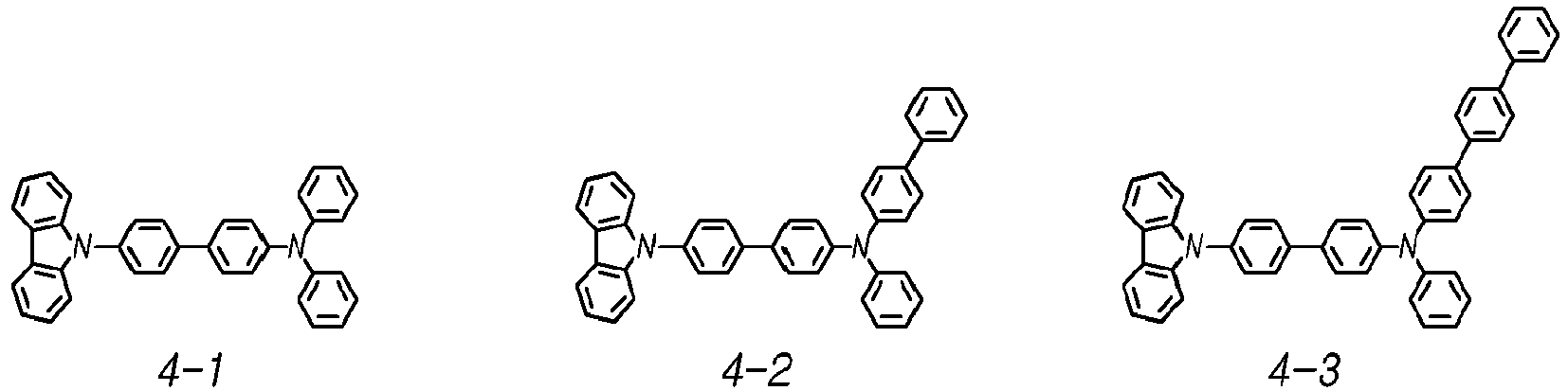


- The first electrode may be an anode electrode, the second electrode may be a cathode electrode, and the first layer may be positioned between the first electrode and the light emitting layer of the organic electric element.
- Furthermore, the first layer may correspond to (i.e. may be identical to) a hole injection layer.
- It is further preferred, if the organic electric element satisfies the following general formula 1:
- [general formula 1] 0.32 eV ≤ L1-H2 ≤ 0.8 eV
- wherein in general formula 1, L1 is the LUMO energy level of the first compound, and H2 is the HOMO (Highest Occupied Molecular Orbital) energy level of the second compound.
- Besides that, it is preferred, if the organic electric element satisfies the following general formula 2:
- [general formula 2] 0.80 eV ≤ L1-H3 ≤ 1.4 eV
- wherein in general formula 2, L1 is the LUMO (Lowest Unoccupied Molecular Orbital) energy level of the first compound, and H3 is the HOMO (Highest Occupied Molecular Orbital) energy level of the third compound.
- It is further preferred, if the organic electric element satisfies the following general formula 3:
- [general formula 3] 0.40 eV ≤ H2-H3 ≤ 0.9 eV
- wherein in general formula 3, H2 is the HOMO (Highest Occupied Molecular Orbital) energy level of the second compound, and H3 is the HOMO (Highest Occupied Molecular Orbital) energy level of the third compound.
- In a second aspect, the invention provides a display panel comprising a subpixel comprising the organic electric element.
- In a third aspect, the invention provides a display device comprising the display panel and a driving circuit for driving the display panel.
- In this way, it is possible to provide the organic electric device having high luminous efficiency and long lifetime.
- Summarizing, it is possible to provide a display panel including the organic electric element having a high luminous efficiency and long lifetime and a display device comprising the same.
- It is to be understood that both the foregoing general description and the following detailed description are exemplary and explanatory and are intended to provide further explanation of the inventive concepts as claimed.
- The above and other objects, features, and advantages of the present invention will be more clearly understood from the following detailed description, taken in conjunction with the accompanying drawings, in which:
-
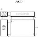
FIG. 1 is a system configuration diagram of a display device according to the present invention; -
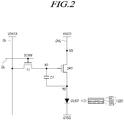
FIG. 2 is a view illustrating a subpixel circuit of a display panel of the present invention; and -
FIG. 3 andFIG.4 are schematic cross-sectional views of an organic electric element of the present invention. - In the following description of examples or embodiments of the present invention, reference will be made to the accompanying drawings in which it is shown by way of illustration specific examples or embodiments that can be implemented, and in which the same reference numerals and signs can be used to designate the same or like components even when they are shown in different accompanying drawings from one another. Further, in the following description of examples or embodiments of the present invention, detailed descriptions of well-known functions and components incorporated herein will be omitted when it is determined that the description may make the subject matter in some embodiments of the present invention rather unclear. The terms such as "including", "having", "containing", "constituting" "make up of', and "formed of" used herein are generally intended to allow other components to be added unless the terms are used with the term "only". As used herein, singular forms are intended to include plural forms unless the context clearly indicates otherwise.
- Terms, such as "first", "second", "A", "B", "(A)", or "(B)" may be used herein to describe elements of the present invention. Each of these terms is not used to define essence, order, sequence, or number of elements etc., but is used merely to distinguish the corresponding element from other elements.
- When it is mentioned that a first element "is connected or coupled to", "contacts or overlaps" etc. a second element, it should be interpreted that, not only can the first element "be directly connected or coupled to" or "directly contact or overlap" the second element, but a third element can also be "interposed" between the first and second elements, or the first and second elements can "be connected or coupled to", "contact or overlap", etc. each other via a fourth element. Here, the second element may be included in at least one of two or more elements that "are connected or coupled to", "contact or overlap", etc. each other.
- When time relative terms, such as "after," "subsequent to," "next," "before," and the like, are used to describe processes or operations of elements or configurations, or flows or steps in operating, processing, manufacturing methods, these terms may be used to describe non-consecutive or non-sequential processes or operations unless the term "directly" or "immediately" is used together.
- In addition, when any dimensions, relative sizes etc. are mentioned, it should be considered that numerical values for an elements or features, or corresponding information (e.g., level, range, etc.) include a tolerance or error range that may be caused by various factors (e.g., process factors, internal or external impact, noise, etc.) even when a relevant description is not specified. Further, the term "may" fully encompasses all the meanings of the term "can".
- The term "halo" or "halogen" as used herein refers to fluorine (F), bromine (Br), chlorine (Cl), or iodine (I) unless otherwise indicated.
- As used herein, the term "alkyl" or "alkyl group" refers to a saturated aliphatic functional radical of 1 to 60 carbon atoms with a single bond therein, including a straight chain alkyl group, a branched chain alkyl group, a cycloalkyl (alicyclic) group, an alkyl-substituted cycloalkyl group, and a cycloalkyl-substituted alkyl group, unless otherwise indicated.
- The term "haloalkyl group" or "halogenalkyl group", as used herein, means a halogensubstituted alkyl group unless otherwise specified.
- The term "heteroalkyl group", as used herein, means that at least one of the carbon atoms constituting the alkyl group has been replaced with a heteroatom.
- As used herein, the terms "alkenyl group" and "alkynyl group", refer to a straight or branched chain of 2 to 60 carbon atoms with a double and a triple bond therein, respectively, unless stated otherwise, but are not limited thereto.
- Unless otherwise stated, the term "cycloalkyl" as used herein refers to an alkyl forming a ring having 3 to 60 carbon atoms, without being limited thereto.
- Unless otherwise stated, the term "alkoxyl group", "alkoxy group", or "alkyloxy group" as used herein means an alkyl group of 1 to 60 carbon atoms having an oxygen radical attached thereto, but is not limited thereto.
- As used herein, the term "alkenoxyl group", "alkenoxy group", "alkenyloxyl group", or "alkenyloxy group" means an alkenyl group of 2 to 60 carbon atoms having an oxygen radical attached thereto, unless otherwise stated, but is not limited thereto.
- As used herein, the term "aryloxyl group" or "aryloxy group" means an aryl group of 6 to 60 carbon atoms having an oxygen radical attached thereto unless otherwise specified, but is not limited thereto.
- As used herein, the terms "aryl group" and "arylene group" each refer to having 6 to 60 carbon atoms unless otherwise stated, but are not limited thereto. In the present invention, an aryl group or an arylene group means a single or multiple aromatic ring, including an aromatic ring which is formed as neighboring substituents participate in a bond or a reaction. For example, the aryl group may be a phenyl group, a biphenyl group, a terphenyl group, a naphthyl group, an anthracenyl group, a fluorene group, a spirofluorene group, or a spirobifluorene group.
- The prefix "aryl" or "ar" means a radical substituted with an aryl group. For example, an arylalkyl group is an alkyl group substituted with an aryl group and an arylalkenyl group is an alkenyl group substituted with an aryl group. In this regard, the radical substituted with an aryl group has the number of carbon atoms described herein.
- Also, when prefixes are named consecutively, it means that the substituents are listed in the order described first. By way of example, an arylalkoxy group means an alkoxy group substituted with an aryl group, an alkoxylcarbonyl group means a carbonyl group substituted with an alkoxyl group, and an arylcarbonylalkenyl group means an alkenyl group substituted with an arylcarbonyl group wherein the arylcarbonyl group is a carbonyl group substituted with an aryl group.
- As used herein, the term "heteroalkyl" means an alkyl bearing one or more heteroatoms unless otherwise indicated. As used herein, the terms "heteroaryl group" and "heteroarylene group" refer respectively to an aryl group and an arylene group of 2 to 60 carbon atoms bearing one or more heteroatoms therein, unless otherwise specified, without being limited thereto. It may include at least one of a single ring and multiple rings, and may be formed by combining adjacent functional groups.
- Unless otherwise indicated, the term "heterocyclic group" as used herein, refers to at least one of heteroaliphatic rings and heteroaromatic rings of 2 to 60 carbon atoms bearing one or more heteroatoms as a ring member thereof, which may be mono- or multi-cyclic and may be formed as neighboring functional groups combine with each other.
- The term "heteroatom" as used herein refers to N, O, S, P, or Si unless otherwise stated.
- "Heterocyclic groups" may also include rings comprising SO2, in place of carbon atoms, as a ring member. For example, a "heterocyclic group" includes the following compounds.

- Unless otherwise stated, the term "aliphatic" as used herein means an aliphatic hydrocarbon of 1 to 60 carbon atoms, and the "aliphatic ring" means an aliphatic hydrocarbon ring of 3 to 60 carbon atoms.
- Unless otherwise stated, the term "ring" as used herein refers to an aliphatic ring of 3 to 60 carbon atoms, an aromatic ring of 6 to 60 carbon atoms, a hetero ring of 2 to 60 carbon atoms, or a fused ring consisting of a combination thereof whether or not it is saturated or unsaturated.
- Other hetero-compounds or hetero-radicals other than the aforementioned hetero-compounds include, but are not limited to, one or more heteroatoms.
- Unless otherwise stated, the term "carbonyl" as used herein is represented by -COR', wherein R' is hydrogen, an alkyl group of 1 to 20 carbon atoms, an aryl group of 6 to 30 carbon atoms, a cycloalkyl group of 3 to 30 carbon atoms, an alkenyl group of 2 to 20 carbon atoms, an alkynyl group of 2 to 20 carbon atoms, or a combination thereof.
- Unless otherwise specified, the term "ether" as used herein is represented by -R-O-R'-, wherein R and R' are each independently hydrogen, an alkyl group of 1 to 20 carbon atoms, an aryl group of 6 to 30 carbon atoms, a cycloalkyl group of 3 to 30 carbon atoms, an alkenyl group of 2 to 20 carbon atoms, an alkynyl group of 2 to 20 carbon atoms, or a combination thereof.
- Also, unless explicitly stated otherwise, the term "substituted" in the expression "substituted or unsubstituted" means having at least one substituent selected from the group consisting of, but not limited to, deuterium, halogen, an amino group, a nitrile group, a nitro group, a C1-C20 alkyl group, a C1-C20 alkoxyl group, a C1-C20 alkylamine group, a C1-C20 alkylthiophene group, a C6-C20 arylthiophene group, a C2-C20 alkenyl group, a C2-C20 alkynyl, a C3-C20 cycloalkyl group, a C6-C20 aryl group, a deuterium-substituted C6-C20 aryl group, a C8-C20 aryl alkenyl group, a silane group, a boron group, a germanium group, and a C2-C20 hetero-ring.
- Also, unless otherwise stated, the chemical formulas used in the present invention are as defined for the exponent parts of the substituent in the following chemical formula:
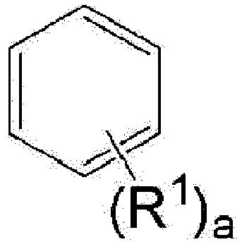
- when a is an integer of 0, the substituent R1 being null,
- when a is an integer of 1, one substituent R1 is bonded to any one of the constituent carbon atoms of the benzene ring,
- when a is an integer of 2 or 3, the substituents R1's, which may be the same or different, are each bonded as represented below, and
- when a is an integer of 4 to 6, the substituents R1's are bonded to the constituents carbon atoms of the benzene ring in the same manner
- while the hydrogens bonded to the constituent carbon atoms of the benzene ring are not indicated:

- In the present specification, the formation of a ring by combining substituents with each other means that adjacent groups combine with each other to form a monocycle or single ring, a ring aggregated or a conjugated multi-cycle, and the monocycle, the ring aggregated and the formed conjugated multicycle may include the heterocycle including at least one heteroatom, and may include aromatic and non-aromatic rings.
- In the present specification, the organic electric element may mean a component(s) between an anode and a cathode, or an organic light emitting diode including the anode, the cathode and the component(s) positioned therebetween.
- In the present specification, the organic electric element may mean one of an organic electric device, the organic light emitting diode and the panel including the same, and an electronic device including the panel and a circuit. For example, the electronic device includes a display device, a lighting device, a solar cell, a portable or mobile terminal (eg, a smart phone, a tablet, a PDA, an electronic dictionary, a PMP, etc.), a navigation terminal, a game machine, various TVs, and various computers monitor and the like, but is not limited thereto, and may be any type of device as long as the component(s) are included.
- Hereinafter, exemplary embodiments of the present invention will be described in detail with reference to the accompanying drawings.
-
FIG. 1 is a system configuration diagram of a display device according to the present inventions. - Referring to
FIG. 1 , thedisplay device 100 includes adisplay panel 110 in which a plurality of data lines DL and a plurality of gate lines GL are arranged and a plurality ofsub-pixels 111 defined by the plurality of data lines DL and the plurality of gate lines GL is arranged, a data driving circuit DDC (or a data driver) for driving the plurality of data lines DL, a gate driving circuit GDC (or a gate driver) for driving the plurality of gate lines GL, a controller D-CTR controlling the data driving circuit DDC and the gate driving circuit GDC, and the like. - The controller D-CTR controls operations of the data driving circuit DDC and the gate driving circuit GDC by supplying respective control signals (DCS, GCS) to the data driving circuit DDC and the gate driving circuit GDC.
- The controller D-CTR starts the scan of pixels according to timings processed in each frame, converts image data inputted from other devices or other image providing sources to be adapted to a data signal form used in the data driving circuit DDC and then outputs image data DATA resulted from the converting, and causes the data to be loaded into the pixels at a preconfigured time according to the scan.
- The controller D-CTR may be implemented as a separate component from the data driving circuit DDC or may be integrated with data driving circuit DDC so the controller D-CTR can be implemented as an integrated circuit.
- The data driving circuit DDC drives the plurality of data lines DL by providing data voltages corresponding to image data DATA received from the controller D-CTR to the data lines DL. Here, the data driving circuit DDC is sometimes referred to as a source driving circuit or a source driver.
- The data driving circuit DDC may include at least one source driver integrated circuit SDIC to be implemented.
- Each source driver integrated circuit SDIC may include a shift register, a latch circuit, a digital to analog converter DAC, an output buffer, and/or the like.
- In some instances, each source driver integrated circuit SDIC may further include one or more analog to digital converters ADC.
- The gate driving circuit GDC sequentially drives a plurality of gate lines GL by sequentially providing scan signals to the plurality of gate lines GL. Here, the gate driving circuit GDC is sometimes referred to as a scan driving circuit or a scan driver.
- The gate driving circuit GDC may include at least one gate driver integrated circuit GDIC to be implemented.
- Each gate driver integrated circuit GDIC may include a shift register, a level shifter, and/or the like.
- Each gate driver integrated circuit GDIC may be connected to a bonding pad of the
display panel 110 in a tape automated bonding (TAB) type or a chip on glass (COG) type, or be directly disposed on thedisplay panel 110 as being implemented in a gate in panel (GIP) type. In some instances, the gate driver integrated circuit GDIC may be disposed to be integrated with thedisplay panel 110. Further, each gate driver integrated circuit GDIC may be implemented in a chip on film (COF) type in which the gate driver integrated circuit GDIC is mounted on a film connected with thedisplay panel 110. - According to the controlling of the controller D-CTR, the gate driving circuit GDC sequentially provides scan signals of an on-voltage or an off-voltage to the plurality of gate lines GL.
- When a specific gate line is asserted by a scan signal from the gate driving circuit GDC, the data driving circuit DDC converts image data DATA received from the controller D-CTR into analog data voltages and provides the obtained analog data voltages to the plurality of data lines DL.
- The data driving circuit DDC may be located on, but not limited to, only one side (e.g., an upper side or a lower side) of the
display panel 110, or in some instances, be located on, but not limited to, two sides (e.g., the upper side and the lower side) of thedisplay panel 110 according to driving schemes, panel design schemes, or the like. - The gate driving circuit GDC may be located on, but not limited to, only one side (e.g., a left side or a right side) of the
panel 110, or in some instances, be located on, but not limited to, two sides (e.g., the left side and the right side) of thedisplay panel 110 according to driving schemes, panel design schemes, or the like. - The
display device 100 according to the present invention may be one of various types of display devices, such as, a liquid crystal display device, an organic light emitting display device, a plasma display device, or the like. - In case the
display device 100 of the present invention is an organic light emitting display device, each sub-pixel 111 arranged in thedisplay panel 110 may include circuit components, such as an organic light emitting diode (OLED), which is a self-emissive element, a driving transistor for driving the organic light emitting diode OLED, and the like. - Types of circuit elements and the number of the circuit elements included in each
subpixel 111 may be different depending on types of the panel (e.g., an LCD panel, an OLED panel, etc.), provided functions, design schemes/features, or the like. -
FIG. 2 is a view illustrating a subpixel circuit of a display panel according to the present invention. - Referring to
FIG. 2 , eachsubpixel 111 may include an organic light emitting diode OLED and a driving transistor DRT for driving the organic light emitting diode OLED as basic circuit components. - Referring to
FIG. 2 , each sub-pixel 111 may further include a first transistor T1 allowing a data voltage VDATA to be applied to a first node N1 corresponding to a gate node of the driving transistor DRT, and a storage capacitor C1 for remaining a data voltage VDATA corresponding to an image signal voltage or a voltage corresponding to this during one frame time. - The organic light emitting diode OLED may be an organic
electric element 220 which may include a first electrode 221 (an anode electrode or a cathode electrode), alight emitting layer 222, a second electrode 223 (the cathode electrode or the anode electrode), and the like. - In one embodiment, a low-level voltage EVSS may be applied to the
second electrode 223 of the organic light emitting diode OLED. - The driving transistor DRT causes the organic light emitting diode OLED to be driven by providing a driving current to the organic light emitting diode OLED.
- The driving transistor DRT includes a first node N1, a second node N2 and a third node N3.
- The first node N1 of the driving transistor DRT may be a node corresponding to the gate node thereof and may be electrically connected to a source node or a drain node of the first transistor T1.
- The second node N2 of the driving transistor DRT may be electrically connected to the
first electrode 221 of the organic light emitting diode OLED and may be a source node or a drain node. - The third node N3 of the driving transistor DRT may be the drain node or the source node as a node to which a driving voltage EVDD is applied, and may be electrically connected to a driving voltage line DVL used to supply a driving voltage EVDD.
- The first transistor T1 may be electrically connected between a data line DL and the first node N1 of the driving transistor DRT and may be controlled by a scan signal SCAN that is provided through a gate line and applied to the gate node of the first transistor T1.
- The storage capacitor C1 may be electrically connected between the first node N1 and the second node N2 of the driving transistor DRT.
- The storage capacitor C1 is an external capacitor intentionally designed to be located outside of the driving transistor DRT, not an internal storage, such as a parasitic capacitor (e.g., a Cgs, a Cgd) that presents between the first node N1 and the second node N2 of the driving transistor DRT.
-
FIG. 3 is a cross-sectional view of an organic electric element according to the present invention. - Referring to
FIG.3 , an organicelectric element 320 includes afirst electrode 321 and asecond electrode 323, anorganic layer 322 positioned therebetween. - The
first electrode 321 may be an anode and thesecond electrode 323 may be a cathode. In the case of an inverted type, thefirst electrode 321 may be a cathode and thesecond electrode 323 may be an anode. - For example, the
first electrode 321 may be a transparent electrode, and thesecond electrode 323 may be a reflective electrode. In another example, thefirst electrode 321 may be a reflective electrode, and thesecond electrode 323 may be a transparent electrode. - The
organic layer 322 may include a plurality of layers which is located between thefirst electrode 321 and thesecond electrode 323 and includes an organic material. - The
organic layer 322 includes alight emitting layer 322a and afirst layer 322b. - The
light emitting layer 322a is a layer in which holes and electrons transmitted from thefirst electrode 321 and thesecond electrode 323 are recombined to emit light, and may include, for example, a host material and a dopant. - The
light emitting layer 322a may include a third compound. The third compound may be, for example, a host material or a dopant included in thelight emitting layer 322a. - The
first layer 322b may be positioned between the light emittinglayer 322a and thefirst electrode 321. For example, thefirst layer 322b may be positioned between thefirst electrode 321 as an anode electrode and thelight emitting layer 322a. - Although not illustrated in
FIG. 3 , the organicelectric device 320 may further include one or more of a hole transport layer, an electron transport layer, and an electron injection layer. For example, the hole transport layer may be positioned between thefirst layer 322b and thelight emitting layer 322a and at the same time between the light emittinglayer 322a and thefirst electrode 321 which serves as an anode electrode. For example, the electron injection layer may be positioned between thesecond electrode 323 which serves as a cathode electrode and thelight emitting layer 322a. For example, the electron transport layer may be positioned between the light emittinglayer 322a and the electron injection layer and at the same time between thesecond electrode 323 which serves as the cathode electrode and thelight emitting layer 322a. In examples including the hole injection layer, thefirst layer 322b may be the hole injection layer. - The
first layer 322b includes a first compound. The hole transport layer may also include the first compound. The first compound included in each layer may be the same or may be different as long as the requirements for the first compound to be described later are met. -
FIG.4 is a view schematically showing an organic electric element according to the present invention. - Referring to
FIG.4 , the organicelectric element 420 includes a first electrode 421, asecond electrode 423, and anorganic layer 422 positioned between the first electrode 421 and thesecond electrode 423. - The first electrode 421 may be, for example, an anode electrode, and the
second electrode 423 may be a cathode electrode. - For example, the first electrode 421 may be a transparent electrode, and the
second electrode 423 may be a reflective electrode. In another example, the first electrode 421 may be a reflective electrode, and thesecond electrode 423 may be a transparent electrode. - The
organic layer 422 is a layer including an organic material while being positioned between the first electrode 421 and thesecond electrode 423 and may be composed of a plurality of layers. - The
organic layer 422 includes afirst stack 424, asecond stack 425, and acharge generating layer 426 positioned between thefirst stack 424 and thesecond stack 425. - The organic
electric element 420 may be a tandem organic electric element including a plurality of stacks each including a light emitting layer. The plurality of light emitting layers may be made of the same material or may be made of different materials. - The
first stack 424 includes a first emittinglayer 424a. The first emittinglayer 424a may include, for example, a host material and a dopant. - The
first stack 424 may further include a firsthole transport layer 424b and a firstelectron transport layer 424b. - The first
hole transport layer 424b may be positioned between the firstlight emitting layer 424a and one of the first electrode 421 and thesecond electrode 423 which serves as an anode electrode. The firstelectron transport layer 424c may be positioned between the firstlight emitting layer 424a and one of the first electrode 421 and thesecond electrode 423 which serves as a cathode electrode. For example, when the first electrode 421 is the anode electrode and thesecond electrode 423 is the cathode electrode, the firsthole transport layer 424b may be positioned on the first electrode 421, the firstlight emitting layer 424a may be positioned on the firsthole transport layer 424b, and the firstelectron transport layer 424c may be positioned on the firstlight emitting layer 424a. - The
second stack 425 includes a second emittinglayer 425a. The second emittinglayer 425a may include, for example, a host material and a dopant. - The
second stack 425 may further include a secondhole transport layer 425b and a second electron transport layer 425c. - The second
hole transport layer 425b may be positioned between the secondlight emitting layer 425a and one of the first electrode 421 and thesecond electrode 423 which serves as an anode electrode. The second electron transport layer 425c may be positioned between the secondlight emitting layer 424a and one of the first electrode 421 and thesecond electrode 423 which serves as a cathode electrode. For example, when the first electrode 421 is the anode electrode and thesecond electrode 423 is the cathode electrode, the secondhole transport layer 425b may be positioned on the second electrode 421, the secondlight emitting layer 425a may be positioned on the secondhole transport layer 425b, and the second electron transport layer 425c may be positioned on the secondlight emitting layer 425a. - Since the
first stack 424 and thesecond stack 425 are configured as described above, holes and electrons transmitted from the first electrode 421 and thesecond electrode 423 recombine in the first and secondlight emitting layers light emitting layers - The
charge generating layer 426 is formed between a plurality of light emitting layers to smoothly distribute charges so that it may increase the current efficiency of the light emitting layer. Accordingly, thecharge generating layer 426 is positioned between thefirst stack 424 including the firstlight emitting layer 424a and thesecond stack 425 including the secondlight emitting layer 425a. - The
charge generating layer 426 may include a p-type charge generating layer and an n-type charge generating layer in order to smoothly distribute charges. For example, thefirst layer 426a may be a p-type charge generating layer and thesecond layer 426b may be an n-type charge generating layer. When the first electrode 421 is the anode electrode and thesecond electrode 423 is the cathode electrode, the p-type charge generating layer may be located on the cathode electrode side and the n-type charge generating layer may be located on the anode side. For example, thefirst layer 426a may be positioned between thesecond layer 426b and thesecond electrode 423 which is a cathode electrode. - Although
FIG. 4 shows a tandem organic electric element including two stacks, the invention is not limited to a tandem organic electric element including two stacks. Instead the invention also comprises organic electric elements with more than two stacks. When the organicelectrical element 420 includes an additional stack, an additional charge generating layer may be positioned between the additional stack and one of the adjacentfirst stack 424 and thesecond stack 425. - The organic
electric element 420 may include ahole injection layer 427. Thehole injection layer 427 may be positioned between the first electrode 421 which serves as an anode electrode and the firstlight emitting layer 424a. For example, thehole injection layer 427 may be positioned between the first electrode 421 which serves as an anode electrode and the firsthole transport layer 424b. - Although not illustrated in
FIG. 4 , the organicelectric element 420 may further include an electron injection layer. For example, the electron injection layer may be positioned between thesecond electrode 423 which serves as a cathode electrode, and the second electron transport layer 425c. - In another example, each of the
first stack 424 and thesecond stack 425 may further include one or more of a hole injection layer and an electron injection layer. Within each stack, the hole injection layer may be located between the light emitting layer and the anode electrode, and an electron injection layer may be located between the light emitting layer and the cathode electrode. - The
first layer 426a includes the first compound. The firsthole transport layer 424b may include the first compound, and the secondhole transport layer 425b may also include the first compound. Further, the hole injection layer may also include the first compound. The first compound included in each layer may be the same or may be different as long as the requirements for the first compound described later are met. - The first compound is represented by one or more of the following chemical formula 1 and chemical formula 2.


- Hereinafter, chemical formula 1 and chemical formula 2 will be described.
- R1 to R6, which are same or different, are each independently one selected from the group consisting of a hydrogen; a deuterium; a tritium; a halogen; a cyano group; a nitro group; a C6-C60 aryl group; a fluorenyl group; a C2-C60 hetero ring group containing at least one hetero atom from O, N, S, Si and P; a fused ring group of a C3-C60 aliphatic ring and a C6-C60 aromatic ring; a C1-C50 alkyl group; a C2-C20 alkenyl group; a C2-C20 alkynyl group; a C1-C30 alkoxy group; a C6-C30 aryloxy group; a C3-C60 alkylsilyl group; a C18-C60 arylsilyl group; and a C8-C60 alkylarylsilyl group, and one or more of R1 to R6 is the cyano group.
- When R1 to R6 are the C6-C60 aryl groups, they may be independently a C6-C30 aryl group or a C6-C12 aryl group.
- A1 to A4, which may be the same or different, are each independently one selected from the group consisting of a hydrogen; a deuterium; a tritium; a halogen; a cyano group; a nitro group; a C6-C60 aryl group; a fluorenyl group; a C2-C60 hetero ring group containing at least one hetero atom from O, N, S, Si and P; a fused ring group of a C3-C60 aliphatic ring and a C6-C60 aromatic ring; a C1-C50 alkyl group; a C2-C20 alkenyl group; a C2-C20 alkynyl group; a C1-C30 alkoxy group; a C6-C30 aryloxy group; a C3-C60 alkylsilyl group; a C18-C60 arylsilyl group; and a C8-C60 alkylarylsilyl group.
- In R1 to R6 and A1 to A4 of chemical formula 1 and chemical formula 2, the C6-C60 aryl group, the fluorenyl group, the C2-C60 hetero ring group containing at least one hetero atom from O, N, S, Si and P, the fused ring group of a C3-C60 aliphatic ring and a C6-C60 aromatic ring, the C1-C50 alkyl group, the C2-C20 alkenyl group, the C2-C20 alkynyl group, the C1-C30 alkoxy group, the C6-C30 aryloxy group, the C3-C60 alkylsilyl group, the C18-C60 arylsilyl group and the C8-C60 alkylarylsilyl group may each be further substituted with at least one substituent selected from the group consisting of a deuterium; a nitro group; a cyano group; a halogen; an amino group; a C1-C20 alkoxyl group; a C1-C20 alkyl group; a C2-C20 alkenyl group; a C2-C20 alkynyl group; a C6-C20 aryl group; a C6-C20 aryl group substituted with the deuterium; a fluorenyl group; a C2-C20 hetero ring group; a C3-C60 alkylsilyl group; a C18-C60 arylsilyl group; and a C8-C60 alkylarylsilyl group.
- When the first compound is represented by one or more of chemical formula 1 and chemical formula 2, for example, the first layer includes one compound (A) represented by chemical formula 1 and one compound (B) represented by chemical formula 2, it means that all the two compounds (A, B) are included in the first compound.
- The
first layer 426a includes a second compound. The second compound is represented by the following chemical formula 3.
- Hereinafter, chemical formula 3 will be described.
- m is an integer from 0 to 4.
- n is an integer from 0 to 3.
- o and p are each independently 0 or 1, o + p is 1 or more. If one of o and p is "0", the other one is not "0".
- R1 is each independently one selected from the group consisting of a deuterium; a tritium; a halogen; a cyano group; a nitro group; a C6-C60 aryl group; a fluorenyl group; a C2-C60 hetero ring group containing at least one hetero atom from O, N, S, Si and P; a fused ring group of a C3-C60 aliphatic ring and a C6-C60 aromatic ring; a C1-C50 alkyl group; a C2-C20 alkenyl group; a C2-C20 alkynyl group; a C1-C30 alkoxy group; a C6-C30 aryloxy group; a C3-C60 alkylsilyl group; a C18-C60 arylsilyl group; and a C8-C60 alkylarylsilyl group.
- When R1 is the C6-C60 aryl group, each may be independently a C6-C30 aryl group or a C6-C12 aryl group.
- R2 and R3, which may be the same or different, are each independently one selected from the group consisting of a C6-C60 aryl group; a fluorenyl group; a C2-C60 hetero ring group containing at least one hetero atom from O, N, S, Si and P; a fused ring group of a C3-C60 aliphatic ring and a C6-C60 aromatic ring; and a C1-C50 alkyl group.
- When R2 and R3 are the C6-C60 aryl groups, they may be each independently a C6-C30 aryl group or a C6-C30 aryl group.
- L1 is one selected from the group consisting of a C6-C60 arylene group; a fluorylene group; a C2-C60 divalent hetero ring group containing at least one heteroatom from O, N, S, Si and P; a divalent fused ring group of a C3-C60 aliphatic ring and a C6-C60 aromatic ring; a C1-C50 alkylene group; a C2-C20 alkenylene group; and a C2-C20 alkynylene group, when p is 1; Alternatively, L1 is ii) one selected from the group consisting of a C6-C60 aryl group; a fluorenyl group; a C2-C60 hetero ring group containing at least one hetero atom from O, N, S, Si and P; a fused ring group of a C3-C60 aliphatic ring and a C6-C60 aromatic ring, when p is 0.
- When L1 is the C6-C60 aryl group, it may be a C6-C30 aryl group or a C6-C12 aryl group.
- When L1 is the C6-C60 arylene group, it may be a C6-C30 arylene group or a C6-C12 arylene group.
- L2 is one selected from the group consisting of a C6-C60 arylene group; a fluorylene group; a C2-C60 divalent hetero ring group containing at least one heteroatom from O, N, S, Si and P; a divalent fused ring group of a C3-C60 aliphatic ring and a C6-C60 aromatic ring; a C1-C50 alkylene group; a C2-C20 alkenylene group; and a C2-C20 alkynylene group, when p is 1; or ii) one selected from the group consisting of a hydrogen; a deuterium; a tritium; a halogen; a cyano group; a nitro group; a C6-C60 aryl group; a fluorenyl group; a C2-C60 hetero ring group containing at least one hetero atom from O, N, S, Si and P; a fused ring group of a C3-C60 aliphatic ring and a C6-C60 aromatic ring; a C1-C50 alkyl group; a C2-C20 alkenyl group; a C2-C20 alkynyl group; a C1-C30 alkoxy group; a C6-C30 aryloxy group; a C3-C60 alkylsilyl group; a C18-C60 arylsilyl group; and a C8-C60 alkylarylsilyl group, when p is 0.
- In R1 to R3, L1 and L2 of chemical formula 3, the C6-C60 aryl group, the fluorenyl group, the C2-C60 hetero ring group containing at least one heteroatom from O, N, S, Si and P, the fused ring group of a C3-C60 aliphatic ring and a C6-C60 aromatic ring, the C1-C50 alkyl group, the C2-C20 alkenyl group, the C2-C20 alkynyl group, the C1-C30 alkoxy group, the C6-C30 aryloxy group, the C3-C60 alkylsilyl group, the C18-C60 arylsilyl group, the C8-C60 alkylarylsilyl group, the C6-C60 arylene group, the fluorylene group, the C1-C50 alkylene group, the C2-C20 alkenylene group, the C2-C20 alkynylene group, the C2-C60 divalent hetero ring group containing at least one heteroatom from O, N, S, Si and P and the divalent fused ring group of a C3-C60 aliphatic ring and a C6-C60 aromatic ring may each be further substituted with at least one substituent selected from the group consisting of a deuterium; a nitro group; a cyano group; a halogen; an amino group; a C1-C20 alkoxyl group; a C1-C20 alkyl group; a C2 - C20 alkenyl group; a C2-C20 alkynyl group; a C6-C20 aryl group; a C6-C20 aryl group substituted with the deuterium; a fluorenyl group; a C2-C20 hetero ring group; a C3-C60 alkylsilyl group; a C18-C60 arylsilyl group; and a C8-C60 alkylarylsilyl group.
- When L2 is the C6-C60 aryl group, it may be a C6-C30 aryl group or a C6-C12 aryl group.
- When L2 is the C6-C60 arylene group, it may be a C6-C30 arylene group or a C6-C12 arylene group.
- Since the organic
electric element 420 includes thefirst layer 426a including the first compound and the second compound, it can have a high efficiency or a long lifetime. - The first chemical compound is represented by one or more of the following chemical formula 4 and chemical formula 5.


- Hereafter, chemical formula 4 and chemical formula 5 will be described.
- n and m are each independently an integer from 0 to 5.
- R7 to R8, which may be the same or different, are each independently one selected from the group consisting of a deuterium; a tritium; a halogen; a cyano group; a C1-C50 alkyl group; and a C1-C30 alkoxy group.
- When R7 and R8 are the C1-C30 alkoxy groups, they may bea C1-C20 alkoxy group or a C1-C10 alkoxy group.
- In R7 and R8 of chemical formula 4 and chemical formula 5, the C1-C50 alkyl group and the C1-C30 alkoxy group may each be further substituted with at least one substituent selected from the group consisting of a deuterium and a halogen.
- When the first compound is represented by one or more of chemical formula 4 and chemical formula 5, for example, the first layer includes one compound (C) represented by chemical formula 4 and one compound (D) represented by chemical formula 5, it means that all the two compounds (C, D) are included in the first compound.
- When the
first layer 426a includes the first compound represented by one or more of the above chemical formulas 4 and 5, the organicelectric element 420 may have high a efficiency or long lifetime. - The first chemical compound is represented by one or more of the following chemical formula 6 and formula 7.


- Below chemical formula 6 and chemical formula 7 will be described in more detail.
- R1 to R6, which are same or different, are each independently one selected from the group consisting of a hydrogen; a deuterium; a tritium; a halogen; a cyano group; a nitro group; a C6-C60 aryl group; a fluorenyl group; a C2-C60 hetero ring group containing at least one hetero atom from O, N, S, Si and P; a fused ring group of a C3-C60 aliphatic ring and a C6-C60 aromatic ring; a C1-C50 alkyl group; a C2-C20 alkenyl group; a C2-C20 alkynyl group; a C1-C30 alkoxy group; a C6-C30 aryloxy group; a C3-C60 alkylsilyl group; a C18-C60 arylsilyl group; and a C8-C60 alkylarylsilyl group, and one or more of R1 to R6 is the cyano group.
- When R1 to R6 are the C6-C60 aryl groups, they may be each independently a C6-C30 aryl group or a C6-C12 aryl group.
- In R1 to R6 of chemical formula 6 and chemical formula 7, the C6-C60 aryl group, the fluorenyl group, the C2-C60 hetero ring group containing at least one hetero atom from O, N, S, Si and P, the fused ring group of a C3-C60 aliphatic ring and a C6-C60 aromatic ring, the C1-C50 alkyl group, the C2-C20 alkenyl group, the C2-C20 alkynyl group, the C1-C30 alkoxy group, the C6-C30 aryloxy group, the C3-C60 alkylsilyl group, the C18-C60 arylsilyl group and the C8-C60 alkylarylsilyl group may each be further substituted with at least one substituent selected from the group consisting of a deuterium; a nitro group; a cyano group; a halogen; an amino group; a C1-C20 alkoxyl group; a C1-C20 alkyl group; a C2 - C20 alkenyl group; a C2-C20 alkynyl group; a C6-C20 aryl group; a C6-C20 aryl group substituted with the deuterium; a fluorenyl group; a C2-C20 hetero ring group; a C3-C60 alkylsilyl group; a C18-C60 arylsilyl group; and a C8-C60 alkylarylsilyl group.
- When the first compound is represented by one or more of chemical formula 7 and chemical formula 8, for example, the first layer includes one compound (E) represented by chemical formula 7 and one compound (F) represented by chemical formula 8, it means that all the two compounds (E, F) are included in the first compound.
- When the
first layer 426a includes the first compound represented by one or more of the above chemical formulas 6 and 7, the organicelectric element 420 may have a high efficiency or a long lifetime. - The first chemical compound may be one or more of the following chemical compounds.


- When the
first layer 426a includes the first compound represented by one or more of the above chemical compounds, the organicelectric element 420 may have a high efficiency or a long lifetime. - The second compound is represented by the following chemical formula 8.


- Hereinafter, chemical formulas 8 and 9 will be described.
- m is an integer from 0 to 4.
- n is an integer from 0 to 3.
- R1 is each independently one selected from the group consisting of a deuterium; a tritium; a halogen; a cyano group; a nitro group; a C6-C60 aryl group; a fluorenyl group; a C2-C60 hetero ring group containing at least one hetero atom from O, N, S, Si and P; a fused ring group of a C3-C60 aliphatic ring and a C6-C60 aromatic ring; a C1-C50 alkyl group; a C2-C20 alkenyl group; a C2-C20 alkynyl group; a C1-C30 alkoxy group; a C6-C30 aryloxy group; a C3-C60 alkylsilyl group; a C18-C60 arylsilyl group; and a C8-C60 alkylarylsilyl group.
- When R1 is the C6-C60 aryl group, it may be each independently a C6-C30 aryl group or a C6-C12 aryl group.
- R2 and R3, which may be the same or different, are each independently one selected from the group consisting of a C6-C60 aryl group; a fluorenyl group; a C2-C60 hetero ring group containing at least one hetero atom from O, N, S, Si and P; a fused ring group of a C3-C60 aliphatic ring and a C6-C60 aromatic ring; a C1-C50 alkyl group.
- When R2 and R3 are the C6-C60 aryl groups, they may be independently a C6-C30 aryl group or a C6-C30 aryl group.
- In chemical formula 8, L1 is one selected from the group consisting of a C6-C60 aryl group; a fluorenyl group; a C2-C60 hetero ring group containing at least one hetero atom from O, N, S, Si and P; a fused ring group of a C3-C60 aliphatic ring and a C6-C60 aromatic ring.
- When L1 is the C6-C60 aryl group, it may be a C6-C30 aryl group or a C6-C12 aryl group.
- In chemical formula 8, L2 is one selected from the group consisting of a C6-C60 arylene group; a fluorylene group; a C2-C60 divalent hetero ring group containing at least one heteroatom from O, N, S, Si and P; a divalent fused ring group of a C3-C60 aliphatic ring and a C6-C60 aromatic ring; a C1-C50 alkylene group; a C2-C20 alkenylene group; and a C2-C20 alkynylene group.
- When L2 is the C6-C60 arylene group, it may be a C6-C30 arylene group or a C6-C12 arylene group.
- In chemical formula 9, L1 is one selected from the group consisting of a C6-C60 arylene group; a fluorylene group; a C2-C60 divalent hetero ring group containing at least one heteroatom from O, N, S, Si and P; a divalent fused ring group of a C3-C60 aliphatic ring and a C6-C60 aromatic ring; a C1-C50 alkylene group; a C2-C20 alkenylene group; and a C2-C20 alkynylene group.
- When L1 is the C6-C60 aryl group, it may be a C6-C30 aryl group or a C6-C12 aryl group.
- In chemical formula 9, L2 is one selected from the group consisting of a C6-C60 aryl group; a fluorenyl group; a C2-C60 hetero ring group containing at least one hetero atom from O, N, S, Si and P; a fused ring group of a C3-C60 aliphatic ring and a C6-C60 aromatic ring.
- When L2 is the C6-C60 aryl group, it may be a C6-C30 aryl group or a C6-C12 aryl group.
- In R1 to R3, L1 and L2 of chemical formula 8 and chemical formula 9, the aryl group, the fluorenyl group, the hetero ring group, the fused ring group, the C1-C50 alkyl group, the C2-C20 alkenyl group, the C2-C20 alkynyl group, the C1-C30 alkoxy group, the C6-C30 aryloxy group, the C3-C60 alkylsilyl group, the C18-C60 arylsilyl group, the C8-C60 alkylarylsilyl group, the C6-C60 arylene group, the fluorylene group, the divalent fused ring group of a C3-C60 aliphatic ring and a C6-C60 aromatic ring, may each be further substituted with at least one substituent selected from the group consisting of a deuterium; a nitro group; a cyano group; a halogen; an amino group; a C1-C20 alkoxyl group; a C1-C20 alkyl group; a C2 - C20 alkenyl group; a C2-C20 alkynyl group; a C6-C20 aryl group; a C6-C20 aryl group substituted with the deuterium; a fluorenyl group; a C2-C20 hetero ring group; a C3-C60 alkylsilyl group; a C18-C60 arylsilyl group; and a C8-C60 alkylarylsilyl group.
- When the second compound is represented by one or more of chemical formula 8 and chemical formula 9, for example, the first layer includes one compound (E) represented by chemical formula 8 and one compound (F) represented by chemical formula 9, it means that all the two compounds (E, F) are included in the first compound.
- When the
first layer 426a includes the first compound and the second compound represented by one or more of the above chemical formulas 8 and 9, the organicelectric element 420 may have a high efficiency or a long lifetime. - The second chemical compound may be one or more of the following chemical compounds.


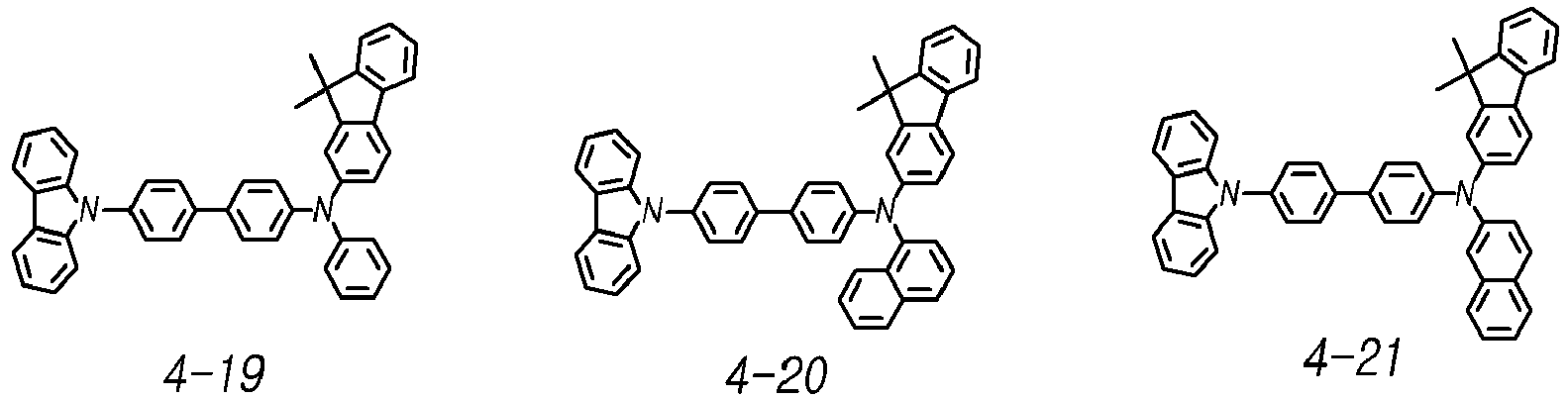

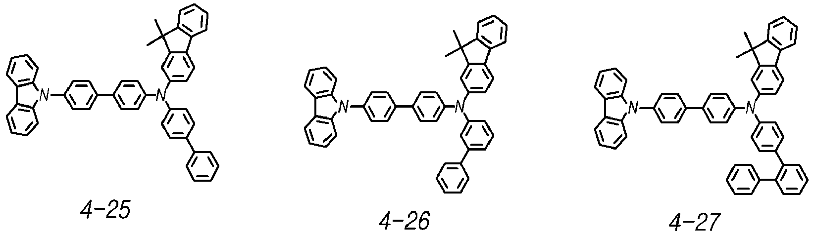


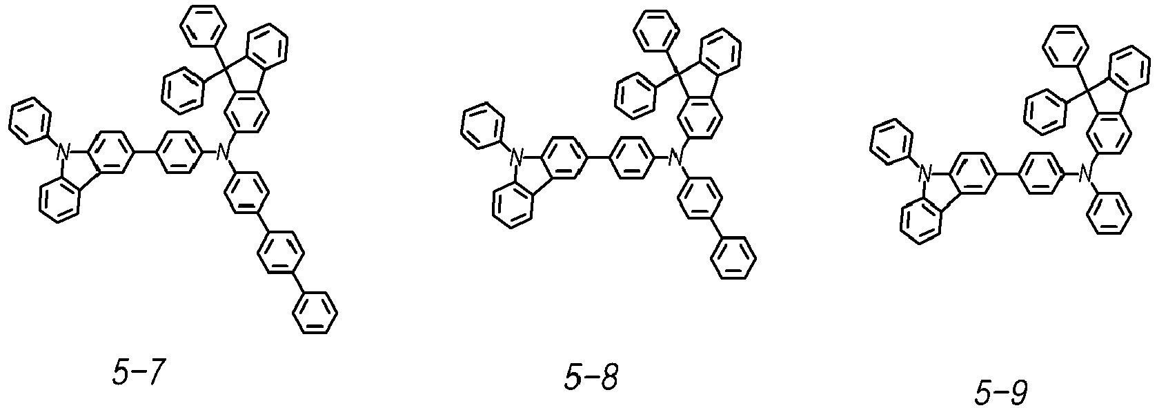


- When the
first layer 426a includes the second compound represented by one or more of the above chemical compounds, the organicelectric element 420 may have a high efficiency or a long lifetime. - The organic
electric element 420 satisfies the following general formula 1.
- In general formula 1, L1 is the LUMO energy level of the first compound. H2 is the HOMO (Highest Occupied Molecular Orbital) energy level of the second compound.
- The lower limit of L1-H2 defined in general formula 1 may be 0.34 eV or more, or 0.38eV or more.
- The upper limit of L1-H2 defined in general formula 1 may be 0.7 eV or less, or 0.6eV or less.
- The organic
electric device 420 includes the first layer including a first compound and a second compound satisfying general formula 1 so that it may have a high efficiency or a long lifetime. - The organic
electric element 420 satisfies the following general formula 2.
- In general formula 2, L1 is the LUMO (Lowest Unoccupied Molecular Orbital) energy level of the first compound.
- H3 is the HOMO (Highest Occupied Molecular Orbital) energy level of the third compound.
- The lower limit of L1-H3 defined in general formula 2 may be 0.90 eV or more, or 1.00eV or more.
- The upper limit of L1-H3 defined in general formula 2 may be 1.3 eV or less, or 1.2 eV or less.
- The organic
electric device 420 includes the first layer including the first compound satisfying general formula 2 and the light emitting layer including the third compound so that it may have a high efficiency or long lifetime. - The organic
electric element 420 satisfies the following general formula 3.
- In general formula 3, H2 is the HOMO (Highest Occupied Molecular Orbital) energy level of the second compound.
- H3 is the HOMO (Highest Occupied Molecular Orbital) energy level of the third compound.
- The lower limit of H2-H3 defined in general formula 3 may be 0.45 eV or more, or 0.50 eV or more.
- The upper limit of H2-H3 defined in general formula 3 may be 0.70 eV or less, or 0.60 eV or less.
- The organic
electric device 420 includes the first layer including the second compound satisfying general formula 3 and the light emitting layer including the third compound so that it may have a high efficiency or a long lifetime. - The first compound included in the
first layer 426a may be a dopant, and the second compound may be a host compound. Since thefirst layer 426a includes the above-described first compound as the dopant and the above-described second compound as the host, thefirst layer 426a has excellent hole transport properties so that the organic electric element may have excellent efficiency and lifespan. - The first compound may be doped at the ratio of 10% to 50% by weight into the
first layer 426a. When the first compound satisfies the above ratio, the first layer has excellent hole transport properties so that the organic electric element may have an excellent efficiency and lifespan. - The thickness of the
first layer 426a is not particularly limited, but may be, for example, 50 Å to 500 Å. - The thickness of the
second layer 426b is not particularly limited, but may be, for example, 50 Å to 500Å. - In another aspect, the present invention provides a
display panel 110. - The
display panel 110 includes a sub-pixel 111 including the above-described organicelectric element 220. - In the
display panel 110 according to the present invention, since the organicelectrical element 220 is the same as the organicelectrical element 220 as described above, a description thereof will be omitted. - In addition, since the
display panel 110 and the sub-pixel 111 according to the embodiments have been described above, a description thereof will be omitted. - Other embodiments of the present invention may provide a
display device 100. - The
display device 100 includes the above-describeddisplay panel 110 and a driving circuit for driving the above-describeddisplay panel 110. - In the
display device 100 according to the present invention, thedisplay panel 110 is the same as thedisplay panel 110 according to the above-described embodiments, so a description thereof will be omitted. - In addition, since the driving circuit for driving the display panel according to embodiments has been described above, a description thereof will be omitted.
- Hereinafter, examples of manufacturing an organic electric element according to the embodiments will be specifically described with reference to the embodiment, but the embodiments are not limited to the following examples.
- After washing a glass substrate coated with ITO (indium tin oxide) to a thickness of 1,000 Å, the substrate is washed with a solvent such as isopropyl alcohol, acetone or methanol and dried. On this prepared ITO transparent electrode, NPD(N, N'-Di(1-naphthyl)-N,N'-diphenyl-(1,1'-biphenyl)-4,4'-diamine) is used as the second compound, F4-TCNQ (2,3,5,6-tetrafluorotetracyanoquinodimethane) was doped with 10% as the first compound and thermally vacuumdeposited to form a hole injection layer of 10 nm. A first hole transport layer (HTL1) was formed by thermal vacuum deposition of a hole transport material (NPD) of 100 nm.
- Subsequently, a second hole transport layer (HTL2) was formed by thermal vacuum deposition of a hole transport material (TCTA, Tris(4-carbazoyl-9-ylphenyl) amine) to a thickness of 100 nm. After that, ADN(9,10-di(naphtha-2-yl)anthracene) and 1,6-Bis (diphenylamine)pyrene were used as host and dopant materials, respectively, doped with 3%, and thermally vacuumdeposited to a thickness of 20 nm to form a first light emitting layer.
- Subsequently, an electron transport layer was formed by thermal vacuum deposition of an electron transport material (TmPyPB, 1,3,5-Tri (m-pyridin-3-ylphenyl) benzene) to a thickness of 10 nm, and Bphen(Bathophenanthroline) as an electron injection material was used, and Li was doped with 2% to form an electron injection layer by thermal vacuum deposition to a thickness of 20 nm. Subsequently, a cathode was formed by depositing Al to a thickness of 50 nm, thereby fabricating an organic electric element.
- The organic electric element was manufactured in the same manner as in the Comparative Example 1, except that the first compound, the second compound and the third compound were used in the types and ratios shown in Table 1 below. Table 2 shows the performances of the manufactured organic electric elements.
[Table 1] first chemical compound second chemical compound third chemical compound L1 -H2 (eV) L1-H3 (eV) H2-H3 (eV) Comparative Example 1 F4-TCNQ(10%) NPD ADN 0.30 0.60 0.30 Comparative Example 2 F4-TCNQ(10%) 4-4 ADN 0.01 0.60 0.59 Comparative Example 3 F4-TCNQ(10%) 4-9 ADN 0.02 0.60 0.58 Comparative Example 4 F4-TCNQ(10%) 4-11 ADN -0.01 0.60 0.61 Comparative Example 5 F4-TCNQ(10%) 5-2 ADN 0 0.60 0.60 Comparative Example 6 F4-TCNQ(10%) 5-8 ADN 0 0.60 0.60 Embodiment 1 A15(10%) NPD ADN 0.76 1.06 0.30 Embodiment 2 A15(10%) 4-4 ADN 0.47 1.06 0.59 Embodiment 3 A15(10%) 4-9 ADN 0.48 1.06 0.58 Embodiment 4 A15(10%) 4-11 ADN 0.45 1.06 0.61 Embodiment 5 A15(10%) 5-2 ADN 0.46 1.06 0.60 Embodiment 6 A15(10%) 5-8 ADN 0.46 1.06 0.60 Embodiment 7 A38(10%) NPD ADN 0.70 1.00 0.30 Embodiment 8 A38(10%) 4-4 ADN 0.41 1.00 0.59 Embodiment 9 A3810% 4-9 ADN 0.42 1.00 0.58 Embodiment 10 A38(10%) 4-11 ADN 0.39 1.00 0.61 Embodiment 11 A38(10%) 5-2 ADN 0.40 1.00 0.60 Embodiment 12 A38(10%) 5-8 ADN 0.40 1.00 0.60 - In Table 1, A15 and A38 are the A15 and A38 chemical compounds described as being selectable as the first chemical compound, and 4-4, 4-9, 4-11, 5-2 and 5-8 are the 4-4, 4-9, 4-11, 5-2 and 5-8 chemical compounds described as being selectable as the second chemical compounds. F4-TCNQ is as follows.

[Table 2] driving voltage efficiency color coordinate lifespan (V) (cd/A) (CIE x, y) (T95, hr) Comparative Example 1 4.79 5.56 0.140 0.097 77 Comparative Example 2 4.69 5.72 0.139 0.098 85 Comparative Example 3 4.70 5.68 0.141 0.099 96 Comparative Example 4 4.64 5.75 0.140 0.100 101 Comparative Example 5 4.70 5.69 0.139 0.099 88 Comparative Example 6 4.68 5.76 0.139 0.098 90 Embodiment 1 4.57 5.95 0.140 0.097 126 Embodiment 2 4.41 6.00 0.140 0.098 171 Embodiment 3 4.30 6.45 0.139 0.099 188 Embodiment 4 4.22 6.22 0.140 0.100 176 Embodiment 5 4.20 6.18 0.139 0.097 160 Embodiment 6 4.24 6.44 0.140 0.097 192 Embodiment 7 4.36 5.97 0.139 0.098 161 Embodiment 8 4.27 6.02 0.141 0.099 218 Embodiment 9 4.26 6.49 0.140 0.100 232 Embodiment 10 4.20 6.27 0.139 0.099 227 Embodiment 11 4.21 6.22 0.139 0.098 215 Embodiment 12 4.19 6.50 0.140 0.099 239 - As can be seen from the results in Table 2, the organic electric elements according to the Inventive Embodiments (i.e. Embodiments 2-6 and 8-12) which include a first layer comprising the first compound and the second compound have an excellent efficiency or lifespan compared to the organic electric element of the Comparative Examples.
- In the case of the organic electric elements in Reference Embodiments 1 and 7 which include a first layer comprising the first compound represented by at least one of chemical formula 1 and chemical formula 2 only, efficiency and lifespan is improved compared to the organic electric elements of the Comparative Embodiments.
- In addition, compared to the Embodiments 1 and 7, it can be seen that the organic electric elements of the Inventive Embodiments (i.e.Embodiments 2-6 and 8-12) which include a first layer that further comprises the second compound represented by chemical formula 3 have a better efficiency and a longer lifetime than the organic electric elements of Embodiments 1 and 7.
- Accordingly, it can be seen that the feature which demands that the first layer comprises a first compound represented by one or more of chemical formulas 1 and 2 and the feature which demands that the first layer comprises a second compound represented by chemical formula 3 provide synergistic effects and assist with providing an improved organic electric element.
Claims (13)
- An organic electric element (220, 320, 420), comprising:a first electrode (221, 321, 421);a second electrode (223, 323, 423); andan organic layer (222, 322, 422) positioned between the first electrode (221, 321, 421) and the second electrode (223, 323, 423),wherein the organic layer (222, 322, 422) comprises a first layer (322b, 426a), andthe first layer (322b, 426a) comprises a first compound represented by one or more of the following chemical formula 1 and chemical formula 2 and a second compound represented by the following chemical formula 3:


 wherein in chemical formula 1 and chemical formula 2,R1 to R6, which are same or different, are each independently one selected from the group consisting of a hydrogen; a deuterium; a tritium; a halogen; a cyano group; a nitro group; a C6-C60 aryl group; a fluorenyl group; a C2-C60 hetero ring group containing at least one hetero atom from O, N, S, Si and P; a fused ring group of a C3-C60 aliphatic ring and a C6-C60 aromatic ring; a C1-C50 alkyl group; a C2-C20 alkenyl group; a C2-C20 alkynyl group; a C1-C30 alkoxy group; a C6-C30 aryloxy group; a C3-C60 alkylsilyl group; a C18-C60 arylsilyl group; and a C8-C60 alkylarylsilyl group, and one or more of R1 to R6 is the cyano group,A1 to A4, which may be the same or different, are each independently one selected from the group consisting of a hydrogen; a deuterium; a tritium; a halogen; a cyano group; a nitro group; a C6-C60 aryl group; a fluorenyl group; a C2-C60 hetero ring group containing at least one hetero atom from O, N, S, Si and P; a fused ring group of a C3-C60 aliphatic ring and a C6-C60 aromatic ring; a C1-C50 alkyl group; a C2-C20 alkenyl group; a C2-C20 alkynyl group; a C1-C30 alkoxy group; a C6-C30 aryloxy group; a C3-C60 alkylsilyl group; a C18-C60 arylsilyl group; and a C8-C60 alkylarylsilyl group,and wherein in R1 to R6 and A1 to A4 of chemical formula 1 and chemical formula 2, the aryl group, the fluorenyl group, the hetero ring group, the fused ring group, the alkyl group, the alkenyl group, the alkynyl group, the alkoxy group, the aryloxy group, the alkylsilyl group, the arylsilyl group and the alkylarylsilyl group may each be further substituted with at least one substituent selected from the group consisting of a deuterium; a nitro group; a cyano group; a halogen; an amino group; a C1-C20 alkoxyl group; a C1-C20 alkyl group; a C2 - C20 alkenyl group; a C2-C20 alkynyl group; a C6-C20 aryl group; a C6-C20 aryl group substituted with the deuterium; a fluorenyl group; a C2-C20 hetero ring group; a C3-C60 alkylsilyl group; a C18-C60 arylsilyl group; and a C8-C60 alkylarylsilyl group,wherein in chemical formula 3,m is an integer from 0 to 4,n is an integer from 0 to 3, ando and p are each independently 0 or 1, o + p is 1 or more,R1 is each independently one selected from the group consisting of a deuterium; a tritium; a halogen; a cyano group; a nitro group; a C6-C60 aryl group; a fluorenyl group; a C2-C60 hetero ring group containing at least one hetero atom from O, N, S, Si and P; a fused ring group of a C3-C60 aliphatic ring and a C6-C60 aromatic ring; a C1-C50 alkyl group; a C2-C20 alkenyl group; a C2-C20 alkynyl group; a C1-C30 alkoxy group; a C6-C30 aryloxy group; a C3-C60 alkylsilyl group; a C18-C60 arylsilyl group; and a C8-C60 alkylarylsilyl group,R2 and R3, which may be the same or different, are each independently one selected from the group consisting of a C6-C60 aryl group; a fluorenyl group; a C2-C60 hetero ring group containing at least one hetero atom from O, N, S, Si and P; a fused ring group of a C3-C60 aliphatic ring and a C6-C60 aromatic ring; a C1-C50 alkyl group,L1 is i) one selected from the group consisting of a C6-C60 arylene group; a fluorylene group; a C2-C60 divalent hetero ring group containing at least one heteroatom from O, N, S, Si and P; a divalent fused ring group of a C3-C60 aliphatic ring and a C6-C60 aromatic ring; a C1-C50 alkylene group; a C2-C20 alkenylene group; and a C2-C20 alkynylene group, when p is 1; ii) one selected from the group consisting of a C6-C60 aryl group; a fluorenyl group; a C2-C60 hetero ring group containing at least one hetero atom from O, N, S, Si and P; a fused ring group of a C3-C60 aliphatic ring and a C6-C60 aromatic ring, when p is 0,L2 is i) one selected from the group consisting of a C6-C60 arylene group; a fluorylene group; a C2-C60 divalent hetero ring group containing at least one heteroatom from O, N, S, Si and P; a divalent fused ring group of a C3-C60 aliphatic ring and a C6-C60 aromatic ring; a C1-C50 alkylene group; a C2-C20 alkenylene group; and a C2-C20 alkynylene group, when p is 1; and ii) one selected from the group consisting of a hydrogen; a deuterium; a tritium; a halogen; a cyano group; a nitro group; a C6-C60 aryl group; a fluorenyl group; a C2-C60 hetero ring group containing at least one hetero atom from O, N, S, Si and P; a fused ring group of a C3-C60 aliphatic ring and a C6-C60 aromatic ring; a C1-C50 alkyl group; a C2-C20 alkenyl group; a C2-C20 alkynyl group; a C1-C30 alkoxy group; a C6-C30 aryloxy group; a C3-C60 alkylsilyl group; a C18-C60 arylsilyl group; and a C8-C60 alkylarylsilyl group, when p is 0,wherein in R1 to R3, L1 and L2 of chemical formula 3, the aryl group, the fluorenyl group, the hetero ring group, the fused ring group, the alkyl group, the alkenyl group, the alkynyl group, the alkoxy group, the aryloxy group, the alkylsilyl group, the arylsilyl group, the alkylarylsilyl group, the arylene group, the fluorylene group, the alkylene group, the alkenylene group and the alkynylene group may each be further substituted with at least one substituent selected from the group consisting of a deuterium; a nitro group; a cyano group; a halogen; an amino group; a C1-C20 alkoxyl group; a C1-C20 alkyl group; a C2 - C20 alkenyl group; a C2-C20 alkynyl group; a C6-C20 aryl group; a C6-C20 aryl group substituted with the deuterium; a fluorenyl group; a C2-C20 hetero ring group; a C3-C60 alkylsilyl group; a C18-C60 arylsilyl group; and a C8-C60 alkylarylsilyl group.
 - The organic electric element (220, 320, 420) according to claim 1, wherein the first chemical compound is represented by one or more of the following chemical formula 4 and chemical formula 5:

 wherein in chemical formula 4 and chemical formula 5,n and m are each independently an integer from 0 to 5,R7 to R8, which may be the same or different, are each independently one selected from the group consisting of a deuterium; a tritium; a halogen; a cyano group; a C1-C50 alkyl group; and a C1-C30 alkoxy group, andwherein the alkyl group and the alkoxy group may each be further substituted with at least one substituent selected from the group consisting of a deuterium and a halogen.
 - The organic electric element (220, 320, 420) according to claim 1 or 2, wherein the first chemical compound is represented by one or more of the following chemical formula 6 and formula 7:

 wherein in chemical formula 6 and chemical formula 7,R1 to R6 are the same as R1 to R6 in chemical formulas 1 and 2.
 - The organic electric element (220, 320, 420) according to one of the preceding claims, wherein the first chemical compound is one or more of the following chemical compounds:








- The organic electric element (220, 320, 420) according to one of the preceding claims, wherein the second chemical compound is represented by one or more of the following chemical formula 9 and formula 10:


 m, n and R1 to R3 are the same as m, n and R1 in chemical formula 3,L1 is one selected from the group consisting of a C6-C60 aryl group; a fluorenyl group; a C2-C60 hetero ring group containing at least one hetero atom from O, N, S, Si and P; a fused ring group of a C3-C60 aliphatic ring and a C6-C60 aromatic ringL2 is one selected from the group consisting of a C6-C60 arylene group; a fluorylene group; a C2-C60 divalent hetero ring group containing at least one heteroatom from O, N, S, Si and P; a divalent fused ring group of a C3-C60 aliphatic ring and a C6-C60 aromatic ring; a C1-C50 alkylene group; a C2-C20 alkenylene group; and a C2-C20 alkynylene group,and wherein in chemical formula 9,m, n and R1 to R3 are the same as m, n and R1 in chemical formula 3,L1 is one selected from the group consisting of a C6-C60 arylene group; a fluorylene group; a C2-C60 divalent hetero ring group containing at least one heteroatom from O, N, S, Si and P; a divalent fused ring group of a C3-C60 aliphatic ring and a C6-C60 aromatic ring; a C1-C50 alkylene group; a C2-C20 alkenylene group; and a C2-C20 alkynylene group,L2 is one selected from the group consisting of a C6-C60 aryl group; a fluorenyl group; a C2-C60 hetero ring group containing at least one hetero atom from O, N, S, Si and P; a fused ring group of a C3-C60 aliphatic ring and a C6-C60 aromatic ring, andwherein in R1 to R3, L1 and L2 of chemical formula 8 and chemical formula 9, the aryl group, the fluorenyl group, the hetero ring group, the fused ring group, the alkyl group, the alkenyl group, the alkynyl group, the alkoxy group, the aryloxy group, the alkylsilyl group, the arylsilyl group, the alkylarylsilyl group, the arylene group, the fluorylene group, the divalent fused ring group, may each be further substituted with at least one substituent selected from the group consisting of a deuterium; a nitro group; a cyano group; a halogen; an amino group; a C1-C20 alkoxyl group; a C1-C20 alkyl group; a C2 - C20 alkenyl group; a C2-C20 alkynyl group; a C6-C20 aryl group; a C6-C20 aryl group substituted with the deuterium; a fluorenyl group; a C2-C20 hetero ring group; a C3-C60 alkylsilyl group; a C18-C60 arylsilyl group; and a C8-C60 alkylarylsilyl group.
 - The organic electric element (220, 320, 420) according to one of the preceding claims, wherein the second chemical compound is one or more of the following chemical compounds:


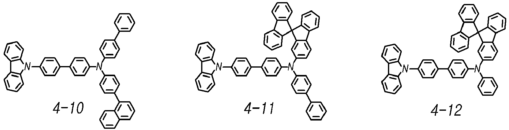

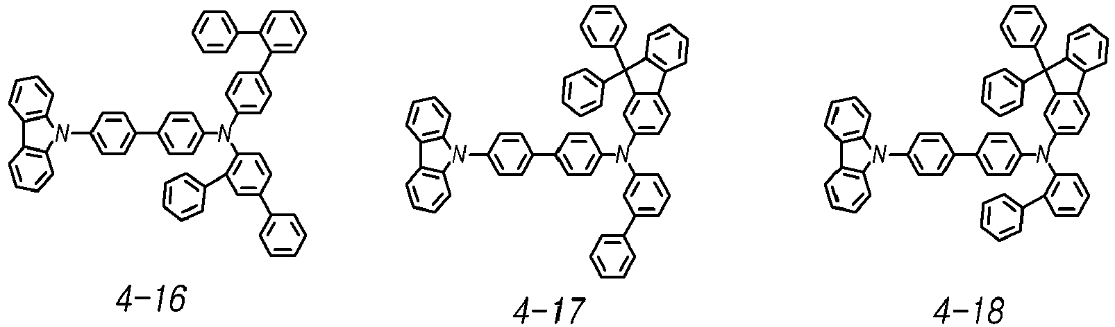


- The organic electric element (320) according to one of the preceding claims, wherein the first electrode (321) is an anode electrode, the second electrode (323) is a cathode electrode, and the first layer (322b) is positioned between the first electrode (321) and the light emitting layer (322a).
- The organic electric element (320) according to one of the preceding claims, wherein the first layer (322b) corresponds to a hole injection layer.
- The organic electric element (220, 320, 420) according to one of the preceding claims, wherein the following general formula 1 is satisfied:

- The organic electric element (220, 320, 420) according to one of the preceding claims, wherein the following general formula 2 is satisfied:

- The organic electric element (220, 320, 420) according to one of the preceding claims, wherein the following general formula 3 is satisfied:

- A display panel (110) comprising a subpixel (111) comprising the organic electric element (220, 320, 420) of one of the preceding claims.
- A display device (100), comprising;the display panel (110) of claim 12; anda driving circuit for driving the display panel (110).
Applications Claiming Priority (1)
| Application Number | Priority Date | Filing Date | Title |
|---|---|---|---|
| KR1020190179906A KR102820114B1 (en) | 2019-12-31 | 2019-12-31 | Organic electronic element, display panel comprising the same and display device comprising the same |
Publications (2)
| Publication Number | Publication Date |
|---|---|
| EP3846242A1 true EP3846242A1 (en) | 2021-07-07 |
| EP3846242B1 EP3846242B1 (en) | 2024-11-13 |
Family
ID=74003761
Family Applications (1)
| Application Number | Title | Priority Date | Filing Date |
|---|---|---|---|
| EP20217608.7A Active EP3846242B1 (en) | 2019-12-31 | 2020-12-29 | Organic electric element, display panel comprising the same and display device comprising the same |
Country Status (4)
| Country | Link |
|---|---|
| US (1) | US20210202860A1 (en) |
| EP (1) | EP3846242B1 (en) |
| KR (1) | KR102820114B1 (en) |
| CN (2) | CN117896992A (en) |
Cited By (1)
| Publication number | Priority date | Publication date | Assignee | Title |
|---|---|---|---|---|
| US11678571B2 (en) | 2006-06-22 | 2023-06-13 | Idemitsu Kosan Co., Ltd. | Organic electroluminescent device using aryl amine derivative containing heterocycle |
Families Citing this family (1)
| Publication number | Priority date | Publication date | Assignee | Title |
|---|---|---|---|---|
| KR20220089235A (en) * | 2020-12-21 | 2022-06-28 | 엘지디스플레이 주식회사 | Organic compound, and Organic light emitting diode and Organic light emitting device including the same |
Citations (2)
| Publication number | Priority date | Publication date | Assignee | Title |
|---|---|---|---|---|
| EP3176844A1 (en) * | 2015-12-03 | 2017-06-07 | LG Display Co., Ltd. | Organic light emitting display device |
| WO2018221871A1 (en) * | 2017-05-31 | 2018-12-06 | 주식회사 엘지화학 | Organic light emitting element |
Family Cites Families (3)
| Publication number | Priority date | Publication date | Assignee | Title |
|---|---|---|---|---|
| US20050123791A1 (en) * | 2003-12-05 | 2005-06-09 | Deaton Joseph C. | Organic electroluminescent devices |
| CN103641726B (en) * | 2005-09-30 | 2015-10-28 | 株式会社半导体能源研究所 | Spirofluorene derivative, light-emitting element material, luminous element, luminaire and electronics |
| KR20100041043A (en) * | 2008-10-13 | 2010-04-22 | 다우어드밴스드디스플레이머티리얼 유한회사 | Novel organic electroluminescent compounds and organic electroluminescent device using the same |
-
2019
- 2019-12-31 KR KR1020190179906A patent/KR102820114B1/en active Active
-
2020
- 2020-12-11 CN CN202311815534.5A patent/CN117896992A/en active Pending
- 2020-12-11 CN CN202011438972.0A patent/CN113130828B/en active Active
- 2020-12-29 EP EP20217608.7A patent/EP3846242B1/en active Active
- 2020-12-30 US US17/138,413 patent/US20210202860A1/en active Pending
Patent Citations (3)
| Publication number | Priority date | Publication date | Assignee | Title |
|---|---|---|---|---|
| EP3176844A1 (en) * | 2015-12-03 | 2017-06-07 | LG Display Co., Ltd. | Organic light emitting display device |
| WO2018221871A1 (en) * | 2017-05-31 | 2018-12-06 | 주식회사 엘지화학 | Organic light emitting element |
| US20200144552A1 (en) * | 2017-05-31 | 2020-05-07 | Lg Chem, Ltd. | Organic light emitting element |
Cited By (1)
| Publication number | Priority date | Publication date | Assignee | Title |
|---|---|---|---|---|
| US11678571B2 (en) | 2006-06-22 | 2023-06-13 | Idemitsu Kosan Co., Ltd. | Organic electroluminescent device using aryl amine derivative containing heterocycle |
Also Published As
| Publication number | Publication date |
|---|---|
| EP3846242B1 (en) | 2024-11-13 |
| US20210202860A1 (en) | 2021-07-01 |
| CN113130828B (en) | 2024-01-19 |
| CN117896992A (en) | 2024-04-16 |
| KR20210086165A (en) | 2021-07-08 |
| CN113130828A (en) | 2021-07-16 |
| KR102820114B1 (en) | 2025-06-13 |
Similar Documents
| Publication | Publication Date | Title |
|---|---|---|
| EP3846241A1 (en) | Organic electric element, display panel comprising the same and display device comprising the same | |
| EP3846240A1 (en) | Organic electric element, display panel comprising the same and display device comprising the same | |
| EP3846239B1 (en) | Organic electric element, display panel comprising the same and display device comprising the same | |
| EP4216697B1 (en) | Organic electric element, display panel comprising the same and display device comprising the same | |
| EP3846242B1 (en) | Organic electric element, display panel comprising the same and display device comprising the same | |
| EP3846238A1 (en) | Organic electric element, display panel comprising the same and display device comprising the same | |
| EP3846237B1 (en) | Organic electric element, display panel comprising the same and display device comprising the same |
Legal Events
| Date | Code | Title | Description |
|---|---|---|---|
| STAA | Information on the status of an ep patent application or granted ep patent |
Free format text: STATUS: REQUEST FOR EXAMINATION WAS MADE |
|
| PUAI | Public reference made under article 153(3) epc to a published international application that has entered the european phase |
Free format text: ORIGINAL CODE: 0009012 |
|
| 17P | Request for examination filed |
Effective date: 20201229 |
|
| AK | Designated contracting states |
Kind code of ref document: A1 Designated state(s): AL AT BE BG CH CY CZ DE DK EE ES FI FR GB GR HR HU IE IS IT LI LT LU LV MC MK MT NL NO PL PT RO RS SE SI SK SM TR |
|
| RBV | Designated contracting states (corrected) |
Designated state(s): AL AT BE BG CH CY CZ DE DK EE ES FI FR GB GR HR HU IE IS IT LI LT LU LV MC MK MT NL NO PL PT RO RS SE SI SK SM TR |
|
| REG | Reference to a national code |
Ref country code: DE Ref legal event code: R079 Free format text: PREVIOUS MAIN CLASS: H01L0051540000 Ipc: H10K0085600000 Ref document number: 602020041230 Country of ref document: DE |
|
| RIC1 | Information provided on ipc code assigned before grant |
Ipc: H10K 85/60 20230101AFI20240423BHEP |
|
| GRAP | Despatch of communication of intention to grant a patent |
Free format text: ORIGINAL CODE: EPIDOSNIGR1 |
|
| STAA | Information on the status of an ep patent application or granted ep patent |
Free format text: STATUS: GRANT OF PATENT IS INTENDED |
|
| RIC1 | Information provided on ipc code assigned before grant |
Ipc: H10K 50/17 20230101ALN20240514BHEP Ipc: H10K 50/14 20230101ALN20240514BHEP Ipc: H10K 85/60 20230101AFI20240514BHEP |
|
| INTG | Intention to grant announced |
Effective date: 20240606 |
|
| RAP3 | Party data changed (applicant data changed or rights of an application transferred) |
Owner name: LG CHEM, LTD. Owner name: LG DISPLAY CO., LTD. |
|
| GRAS | Grant fee paid |
Free format text: ORIGINAL CODE: EPIDOSNIGR3 |
|
| GRAA | (expected) grant |
Free format text: ORIGINAL CODE: 0009210 |
|
| STAA | Information on the status of an ep patent application or granted ep patent |
Free format text: STATUS: THE PATENT HAS BEEN GRANTED |
|
| AK | Designated contracting states |
Kind code of ref document: B1 Designated state(s): AL AT BE BG CH CY CZ DE DK EE ES FI FR GB GR HR HU IE IS IT LI LT LU LV MC MK MT NL NO PL PT RO RS SE SI SK SM TR |
|
| REG | Reference to a national code |
Ref country code: GB Ref legal event code: FG4D |
|
| REG | Reference to a national code |
Ref country code: CH Ref legal event code: EP |
|
| REG | Reference to a national code |
Ref country code: IE Ref legal event code: FG4D |
|
| REG | Reference to a national code |
Ref country code: DE Ref legal event code: R096 Ref document number: 602020041230 Country of ref document: DE |
|
| REG | Reference to a national code |
Ref country code: LT Ref legal event code: MG9D |
|
| REG | Reference to a national code |
Ref country code: NL Ref legal event code: MP Effective date: 20241113 |
|
| PG25 | Lapsed in a contracting state [announced via postgrant information from national office to epo] |
Ref country code: PT Free format text: LAPSE BECAUSE OF FAILURE TO SUBMIT A TRANSLATION OF THE DESCRIPTION OR TO PAY THE FEE WITHIN THE PRESCRIBED TIME-LIMIT Effective date: 20250313 Ref country code: HR Free format text: LAPSE BECAUSE OF FAILURE TO SUBMIT A TRANSLATION OF THE DESCRIPTION OR TO PAY THE FEE WITHIN THE PRESCRIBED TIME-LIMIT Effective date: 20241113 Ref country code: IS Free format text: LAPSE BECAUSE OF FAILURE TO SUBMIT A TRANSLATION OF THE DESCRIPTION OR TO PAY THE FEE WITHIN THE PRESCRIBED TIME-LIMIT Effective date: 20250313 |
|
| PG25 | Lapsed in a contracting state [announced via postgrant information from national office to epo] |
Ref country code: FI Free format text: LAPSE BECAUSE OF FAILURE TO SUBMIT A TRANSLATION OF THE DESCRIPTION OR TO PAY THE FEE WITHIN THE PRESCRIBED TIME-LIMIT Effective date: 20241113 Ref country code: NL Free format text: LAPSE BECAUSE OF FAILURE TO SUBMIT A TRANSLATION OF THE DESCRIPTION OR TO PAY THE FEE WITHIN THE PRESCRIBED TIME-LIMIT Effective date: 20241113 |
|
| REG | Reference to a national code |
Ref country code: AT Ref legal event code: MK05 Ref document number: 1742652 Country of ref document: AT Kind code of ref document: T Effective date: 20241113 |
|
| PG25 | Lapsed in a contracting state [announced via postgrant information from national office to epo] |
Ref country code: BG Free format text: LAPSE BECAUSE OF FAILURE TO SUBMIT A TRANSLATION OF THE DESCRIPTION OR TO PAY THE FEE WITHIN THE PRESCRIBED TIME-LIMIT Effective date: 20241113 |
|
| PG25 | Lapsed in a contracting state [announced via postgrant information from national office to epo] |
Ref country code: ES Free format text: LAPSE BECAUSE OF FAILURE TO SUBMIT A TRANSLATION OF THE DESCRIPTION OR TO PAY THE FEE WITHIN THE PRESCRIBED TIME-LIMIT Effective date: 20241113 |
|
| PG25 | Lapsed in a contracting state [announced via postgrant information from national office to epo] |
Ref country code: NO Free format text: LAPSE BECAUSE OF FAILURE TO SUBMIT A TRANSLATION OF THE DESCRIPTION OR TO PAY THE FEE WITHIN THE PRESCRIBED TIME-LIMIT Effective date: 20250213 |
|
| PG25 | Lapsed in a contracting state [announced via postgrant information from national office to epo] |
Ref country code: LV Free format text: LAPSE BECAUSE OF FAILURE TO SUBMIT A TRANSLATION OF THE DESCRIPTION OR TO PAY THE FEE WITHIN THE PRESCRIBED TIME-LIMIT Effective date: 20241113 Ref country code: AT Free format text: LAPSE BECAUSE OF FAILURE TO SUBMIT A TRANSLATION OF THE DESCRIPTION OR TO PAY THE FEE WITHIN THE PRESCRIBED TIME-LIMIT Effective date: 20241113 Ref country code: GR Free format text: LAPSE BECAUSE OF FAILURE TO SUBMIT A TRANSLATION OF THE DESCRIPTION OR TO PAY THE FEE WITHIN THE PRESCRIBED TIME-LIMIT Effective date: 20250214 |
|
| PG25 | Lapsed in a contracting state [announced via postgrant information from national office to epo] |
Ref country code: PL Free format text: LAPSE BECAUSE OF FAILURE TO SUBMIT A TRANSLATION OF THE DESCRIPTION OR TO PAY THE FEE WITHIN THE PRESCRIBED TIME-LIMIT Effective date: 20241113 |
|
| PG25 | Lapsed in a contracting state [announced via postgrant information from national office to epo] |
Ref country code: RS Free format text: LAPSE BECAUSE OF FAILURE TO SUBMIT A TRANSLATION OF THE DESCRIPTION OR TO PAY THE FEE WITHIN THE PRESCRIBED TIME-LIMIT Effective date: 20250213 |
|
| PG25 | Lapsed in a contracting state [announced via postgrant information from national office to epo] |
Ref country code: SM Free format text: LAPSE BECAUSE OF FAILURE TO SUBMIT A TRANSLATION OF THE DESCRIPTION OR TO PAY THE FEE WITHIN THE PRESCRIBED TIME-LIMIT Effective date: 20241113 |
|
| PG25 | Lapsed in a contracting state [announced via postgrant information from national office to epo] |
Ref country code: DK Free format text: LAPSE BECAUSE OF FAILURE TO SUBMIT A TRANSLATION OF THE DESCRIPTION OR TO PAY THE FEE WITHIN THE PRESCRIBED TIME-LIMIT Effective date: 20241113 |
|
| PG25 | Lapsed in a contracting state [announced via postgrant information from national office to epo] |
Ref country code: EE Free format text: LAPSE BECAUSE OF FAILURE TO SUBMIT A TRANSLATION OF THE DESCRIPTION OR TO PAY THE FEE WITHIN THE PRESCRIBED TIME-LIMIT Effective date: 20241113 |
|
| PG25 | Lapsed in a contracting state [announced via postgrant information from national office to epo] |
Ref country code: RO Free format text: LAPSE BECAUSE OF FAILURE TO SUBMIT A TRANSLATION OF THE DESCRIPTION OR TO PAY THE FEE WITHIN THE PRESCRIBED TIME-LIMIT Effective date: 20241113 |
|
| PG25 | Lapsed in a contracting state [announced via postgrant information from national office to epo] |
Ref country code: SK Free format text: LAPSE BECAUSE OF FAILURE TO SUBMIT A TRANSLATION OF THE DESCRIPTION OR TO PAY THE FEE WITHIN THE PRESCRIBED TIME-LIMIT Effective date: 20241113 |
|
| PG25 | Lapsed in a contracting state [announced via postgrant information from national office to epo] |
Ref country code: CZ Free format text: LAPSE BECAUSE OF FAILURE TO SUBMIT A TRANSLATION OF THE DESCRIPTION OR TO PAY THE FEE WITHIN THE PRESCRIBED TIME-LIMIT Effective date: 20241113 |
|
| PG25 | Lapsed in a contracting state [announced via postgrant information from national office to epo] |
Ref country code: IT Free format text: LAPSE BECAUSE OF FAILURE TO SUBMIT A TRANSLATION OF THE DESCRIPTION OR TO PAY THE FEE WITHIN THE PRESCRIBED TIME-LIMIT Effective date: 20241113 |
|
| REG | Reference to a national code |
Ref country code: CH Ref legal event code: PL |
|
| REG | Reference to a national code |
Ref country code: DE Ref legal event code: R097 Ref document number: 602020041230 Country of ref document: DE |
|
| PG25 | Lapsed in a contracting state [announced via postgrant information from national office to epo] |
Ref country code: LU Free format text: LAPSE BECAUSE OF NON-PAYMENT OF DUE FEES Effective date: 20241229 |
|
| PG25 | Lapsed in a contracting state [announced via postgrant information from national office to epo] |
Ref country code: SE Free format text: LAPSE BECAUSE OF FAILURE TO SUBMIT A TRANSLATION OF THE DESCRIPTION OR TO PAY THE FEE WITHIN THE PRESCRIBED TIME-LIMIT Effective date: 20241113 |
|
| PG25 | Lapsed in a contracting state [announced via postgrant information from national office to epo] |
Ref country code: MC Free format text: LAPSE BECAUSE OF FAILURE TO SUBMIT A TRANSLATION OF THE DESCRIPTION OR TO PAY THE FEE WITHIN THE PRESCRIBED TIME-LIMIT Effective date: 20241113 |
|
| PLBE | No opposition filed within time limit |
Free format text: ORIGINAL CODE: 0009261 |
|
| STAA | Information on the status of an ep patent application or granted ep patent |
Free format text: STATUS: NO OPPOSITION FILED WITHIN TIME LIMIT |
|
| REG | Reference to a national code |
Ref country code: BE Ref legal event code: MM Effective date: 20241231 |
|
| PG25 | Lapsed in a contracting state [announced via postgrant information from national office to epo] |
Ref country code: BE Free format text: LAPSE BECAUSE OF NON-PAYMENT OF DUE FEES Effective date: 20241231 |
|
| PG25 | Lapsed in a contracting state [announced via postgrant information from national office to epo] |
Ref country code: CH Free format text: LAPSE BECAUSE OF NON-PAYMENT OF DUE FEES Effective date: 20241231 |
|
| 26N | No opposition filed |
Effective date: 20250814 |
|
| PG25 | Lapsed in a contracting state [announced via postgrant information from national office to epo] |
Ref country code: IE Free format text: LAPSE BECAUSE OF NON-PAYMENT OF DUE FEES Effective date: 20241229 |
|
| PGFP | Annual fee paid to national office [announced via postgrant information from national office to epo] |
Ref country code: DE Payment date: 20251020 Year of fee payment: 6 |
|
| PGFP | Annual fee paid to national office [announced via postgrant information from national office to epo] |
Ref country code: GB Payment date: 20251023 Year of fee payment: 6 |
|
| PGFP | Annual fee paid to national office [announced via postgrant information from national office to epo] |
Ref country code: FR Payment date: 20251021 Year of fee payment: 6 |
|
| PG25 | Lapsed in a contracting state [announced via postgrant information from national office to epo] |
Ref country code: CY Free format text: LAPSE BECAUSE OF FAILURE TO SUBMIT A TRANSLATION OF THE DESCRIPTION OR TO PAY THE FEE WITHIN THE PRESCRIBED TIME-LIMIT Effective date: 20241113 |