EP3176844A1 - Organic light emitting display device - Google Patents
Organic light emitting display device Download PDFInfo
- Publication number
- EP3176844A1 EP3176844A1 EP16182682.1A EP16182682A EP3176844A1 EP 3176844 A1 EP3176844 A1 EP 3176844A1 EP 16182682 A EP16182682 A EP 16182682A EP 3176844 A1 EP3176844 A1 EP 3176844A1
- Authority
- EP
- European Patent Office
- Prior art keywords
- light emitting
- group
- layer
- carbon atoms
- hole injection
- Prior art date
- Legal status (The legal status is an assumption and is not a legal conclusion. Google has not performed a legal analysis and makes no representation as to the accuracy of the status listed.)
- Granted
Links
- 239000010410 layer Substances 0.000 claims abstract description 539
- 150000001875 compounds Chemical class 0.000 claims abstract description 157
- 125000004432 carbon atom Chemical group C* 0.000 claims abstract description 63
- 125000004093 cyano group Chemical group *C#N 0.000 claims abstract description 19
- 239000000126 substance Substances 0.000 claims abstract description 19
- 125000000217 alkyl group Chemical group 0.000 claims abstract description 18
- 125000003118 aryl group Chemical group 0.000 claims abstract description 18
- 239000012044 organic layer Substances 0.000 claims abstract description 18
- 229910052757 nitrogen Inorganic materials 0.000 claims abstract description 16
- 125000005842 heteroatom Chemical group 0.000 claims abstract description 15
- 125000003545 alkoxy group Chemical group 0.000 claims abstract description 14
- 125000001033 ether group Chemical group 0.000 claims abstract description 14
- 125000001153 fluoro group Chemical group F* 0.000 claims abstract description 14
- 125000001072 heteroaryl group Chemical group 0.000 claims abstract description 14
- 229910052760 oxygen Inorganic materials 0.000 claims abstract description 14
- 229910052710 silicon Inorganic materials 0.000 claims abstract description 14
- 229910052717 sulfur Inorganic materials 0.000 claims abstract description 14
- 125000000876 trifluoromethoxy group Chemical group FC(F)(F)O* 0.000 claims abstract description 14
- 125000002023 trifluoromethyl group Chemical group FC(F)(F)* 0.000 claims abstract description 14
- 125000000026 trimethylsilyl group Chemical group [H]C([H])([H])[Si]([*])(C([H])([H])[H])C([H])([H])[H] 0.000 claims abstract description 14
- 125000004435 hydrogen atom Chemical group [H]* 0.000 claims abstract description 10
- 238000002347 injection Methods 0.000 claims description 188
- 239000007924 injection Substances 0.000 claims description 188
- 239000002019 doping agent Substances 0.000 claims description 27
- 125000001424 substituent group Chemical group 0.000 claims description 24
- 125000004404 heteroalkyl group Chemical group 0.000 claims description 4
- 230000005525 hole transport Effects 0.000 description 60
- YMWUJEATGCHHMB-UHFFFAOYSA-N Dichloromethane Chemical compound ClCCl YMWUJEATGCHHMB-UHFFFAOYSA-N 0.000 description 54
- 230000000052 comparative effect Effects 0.000 description 38
- 239000000463 material Substances 0.000 description 33
- CSNNHWWHGAXBCP-UHFFFAOYSA-L Magnesium sulfate Chemical compound [Mg+2].[O-][S+2]([O-])([O-])[O-] CSNNHWWHGAXBCP-UHFFFAOYSA-L 0.000 description 32
- 238000004770 highest occupied molecular orbital Methods 0.000 description 27
- 238000004768 lowest unoccupied molecular orbital Methods 0.000 description 23
- DKHNGUNXLDCATP-UHFFFAOYSA-N dipyrazino[2,3-f:2',3'-h]quinoxaline-2,3,6,7,10,11-hexacarbonitrile Chemical compound C12=NC(C#N)=C(C#N)N=C2C2=NC(C#N)=C(C#N)N=C2C2=C1N=C(C#N)C(C#N)=N2 DKHNGUNXLDCATP-UHFFFAOYSA-N 0.000 description 22
- 230000008021 deposition Effects 0.000 description 21
- 0 CCC(C)C=C(C)C(C1=CC(C)(*)C(C(C)CC(*)c2cc(N)cc([Zn])c2)=C(C)C1C(*)c1cc([Zn]C)cc(*)c1)=* Chemical compound CCC(C)C=C(C)C(C1=CC(C)(*)C(C(C)CC(*)c2cc(N)cc([Zn])c2)=C(C)C1C(*)c1cc([Zn]C)cc(*)c1)=* 0.000 description 20
- NLXLAEXVIDQMFP-UHFFFAOYSA-N Ammonia chloride Chemical compound [NH4+].[Cl-] NLXLAEXVIDQMFP-UHFFFAOYSA-N 0.000 description 18
- YBYIRNPNPLQARY-UHFFFAOYSA-N 1H-indene Chemical compound C1=CC=C2CC=CC2=C1 YBYIRNPNPLQARY-UHFFFAOYSA-N 0.000 description 16
- 229910052943 magnesium sulfate Inorganic materials 0.000 description 16
- 238000000034 method Methods 0.000 description 16
- 230000008569 process Effects 0.000 description 15
- 239000000203 mixture Substances 0.000 description 14
- 238000000605 extraction Methods 0.000 description 12
- 229910052782 aluminium Inorganic materials 0.000 description 9
- XAGFODPZIPBFFR-UHFFFAOYSA-N aluminium Chemical compound [Al] XAGFODPZIPBFFR-UHFFFAOYSA-N 0.000 description 9
- 238000012546 transfer Methods 0.000 description 9
- JUJWROOIHBZHMG-UHFFFAOYSA-N Pyridine Chemical compound C1=CC=NC=C1 JUJWROOIHBZHMG-UHFFFAOYSA-N 0.000 description 8
- 230000015572 biosynthetic process Effects 0.000 description 8
- 238000004440 column chromatography Methods 0.000 description 8
- UAOMVDZJSHZZME-UHFFFAOYSA-N diisopropylamine Chemical compound CC(C)NC(C)C UAOMVDZJSHZZME-UHFFFAOYSA-N 0.000 description 8
- 230000006872 improvement Effects 0.000 description 8
- 235000019341 magnesium sulphate Nutrition 0.000 description 8
- 239000007787 solid Substances 0.000 description 8
- XJDNKRIXUMDJCW-UHFFFAOYSA-J titanium tetrachloride Chemical compound Cl[Ti](Cl)(Cl)Cl XJDNKRIXUMDJCW-UHFFFAOYSA-J 0.000 description 8
- RIOQSEWOXXDEQQ-UHFFFAOYSA-N triphenylphosphine Chemical compound C1=CC=CC=C1P(C=1C=CC=CC=1)C1=CC=CC=C1 RIOQSEWOXXDEQQ-UHFFFAOYSA-N 0.000 description 8
- 238000004519 manufacturing process Methods 0.000 description 7
- 238000003786 synthesis reaction Methods 0.000 description 7
- XEKOWRVHYACXOJ-UHFFFAOYSA-N Ethyl acetate Chemical compound CCOC(C)=O XEKOWRVHYACXOJ-UHFFFAOYSA-N 0.000 description 6
- XLOMVQKBTHCTTD-UHFFFAOYSA-N Zinc monoxide Chemical compound [Zn]=O XLOMVQKBTHCTTD-UHFFFAOYSA-N 0.000 description 6
- 235000019270 ammonium chloride Nutrition 0.000 description 6
- 239000000243 solution Substances 0.000 description 6
- 239000007983 Tris buffer Substances 0.000 description 5
- 238000002360 preparation method Methods 0.000 description 5
- WSLDOOZREJYCGB-UHFFFAOYSA-N 1,2-Dichloroethane Chemical group ClCCCl WSLDOOZREJYCGB-UHFFFAOYSA-N 0.000 description 4
- AOIJDQAFSCJFIO-UHFFFAOYSA-N 2,6-bis(4-cyanophenyl)-3,7-dioxo-s-indacene-1,5-dicarbonitrile Chemical compound C(#N)C1=CC=C(C=C1)C1=C(C2=CC=3C(C(=C(C=3C=C2C1=O)C#N)C1=CC=C(C=C1)C#N)=O)C#N AOIJDQAFSCJFIO-UHFFFAOYSA-N 0.000 description 4
- 239000012300 argon atmosphere Substances 0.000 description 4
- YNHIGQDRGKUECZ-UHFFFAOYSA-L bis(triphenylphosphine)palladium(ii) dichloride Chemical compound [Cl-].[Cl-].[Pd+2].C1=CC=CC=C1P(C=1C=CC=CC=1)C1=CC=CC=C1.C1=CC=CC=C1P(C=1C=CC=CC=1)C1=CC=CC=C1 YNHIGQDRGKUECZ-UHFFFAOYSA-L 0.000 description 4
- 239000011575 calcium Substances 0.000 description 4
- 238000006243 chemical reaction Methods 0.000 description 4
- NEHMKBQYUWJMIP-UHFFFAOYSA-N chloromethane Chemical compound ClC NEHMKBQYUWJMIP-UHFFFAOYSA-N 0.000 description 4
- GBRBMTNGQBKBQE-UHFFFAOYSA-L copper;diiodide Chemical compound I[Cu]I GBRBMTNGQBKBQE-UHFFFAOYSA-L 0.000 description 4
- 239000011777 magnesium Substances 0.000 description 4
- PIBWKRNGBLPSSY-UHFFFAOYSA-L palladium(II) chloride Chemical compound Cl[Pd]Cl PIBWKRNGBLPSSY-UHFFFAOYSA-L 0.000 description 4
- UMJSCPRVCHMLSP-UHFFFAOYSA-N pyridine Natural products COC1=CC=CN=C1 UMJSCPRVCHMLSP-UHFFFAOYSA-N 0.000 description 4
- 239000000758 substrate Substances 0.000 description 4
- 238000012360 testing method Methods 0.000 description 4
- TVIVIEFSHFOWTE-UHFFFAOYSA-K tri(quinolin-8-yloxy)alumane Chemical compound [Al+3].C1=CN=C2C([O-])=CC=CC2=C1.C1=CN=C2C([O-])=CC=CC2=C1.C1=CN=C2C([O-])=CC=CC2=C1 TVIVIEFSHFOWTE-UHFFFAOYSA-K 0.000 description 4
- MAGZFXHVHHEINI-UHFFFAOYSA-N 1,5-bis(chloromethyl)-2,4-bis(2-phenylethynyl)benzene Chemical compound ClCC1=C(C=C(C(=C1)CCl)C#CC1=CC=CC=C1)C#CC1=CC=CC=C1 MAGZFXHVHHEINI-UHFFFAOYSA-N 0.000 description 3
- IXHWGNYCZPISET-UHFFFAOYSA-N 2-[4-(dicyanomethylidene)-2,3,5,6-tetrafluorocyclohexa-2,5-dien-1-ylidene]propanedinitrile Chemical compound FC1=C(F)C(=C(C#N)C#N)C(F)=C(F)C1=C(C#N)C#N IXHWGNYCZPISET-UHFFFAOYSA-N 0.000 description 3
- WEVYAHXRMPXWCK-UHFFFAOYSA-N Acetonitrile Chemical compound CC#N WEVYAHXRMPXWCK-UHFFFAOYSA-N 0.000 description 3
- 238000003775 Density Functional Theory Methods 0.000 description 3
- PXHVJJICTQNCMI-UHFFFAOYSA-N Nickel Chemical compound [Ni] PXHVJJICTQNCMI-UHFFFAOYSA-N 0.000 description 3
- UFVXQDWNSAGPHN-UHFFFAOYSA-K bis[(2-methylquinolin-8-yl)oxy]-(4-phenylphenoxy)alumane Chemical compound [Al+3].C1=CC=C([O-])C2=NC(C)=CC=C21.C1=CC=C([O-])C2=NC(C)=CC=C21.C1=CC([O-])=CC=C1C1=CC=CC=C1 UFVXQDWNSAGPHN-UHFFFAOYSA-K 0.000 description 3
- 229910052791 calcium Inorganic materials 0.000 description 3
- 238000005304 joining Methods 0.000 description 3
- 229910052749 magnesium Inorganic materials 0.000 description 3
- 150000002736 metal compounds Chemical class 0.000 description 3
- 235000012736 patent blue V Nutrition 0.000 description 3
- -1 polyphenylenevinylene Polymers 0.000 description 3
- 239000011787 zinc oxide Substances 0.000 description 3
- NGQSLSMAEVWNPU-YTEMWHBBSA-N 1,2-bis[(e)-2-phenylethenyl]benzene Chemical compound C=1C=CC=CC=1/C=C/C1=CC=CC=C1\C=C\C1=CC=CC=C1 NGQSLSMAEVWNPU-YTEMWHBBSA-N 0.000 description 2
- UCPMCOZDCIXZFU-UHFFFAOYSA-N 3,5-dioxo-2,6-diphenyl-s-indacene-1,7-dicarbonitrile Chemical compound O=C1C(=C(C2=CC=3C(=C(C(C=3C=C12)=O)C1=CC=CC=C1)C#N)C#N)C1=CC=CC=C1 UCPMCOZDCIXZFU-UHFFFAOYSA-N 0.000 description 2
- VFUDMQLBKNMONU-UHFFFAOYSA-N 9-[4-(4-carbazol-9-ylphenyl)phenyl]carbazole Chemical compound C12=CC=CC=C2C2=CC=CC=C2N1C1=CC=C(C=2C=CC(=CC=2)N2C3=CC=CC=C3C3=CC=CC=C32)C=C1 VFUDMQLBKNMONU-UHFFFAOYSA-N 0.000 description 2
- JJHHIJFTHRNPIK-UHFFFAOYSA-N Diphenyl sulfoxide Chemical compound C=1C=CC=CC=1S(=O)C1=CC=CC=C1 JJHHIJFTHRNPIK-UHFFFAOYSA-N 0.000 description 2
- 229910052693 Europium Inorganic materials 0.000 description 2
- 229920001609 Poly(3,4-ethylenedioxythiophene) Polymers 0.000 description 2
- BQCADISMDOOEFD-UHFFFAOYSA-N Silver Chemical compound [Ag] BQCADISMDOOEFD-UHFFFAOYSA-N 0.000 description 2
- 229910052769 Ytterbium Inorganic materials 0.000 description 2
- 229910052784 alkaline earth metal Inorganic materials 0.000 description 2
- FJDQFPXHSGXQBY-UHFFFAOYSA-L caesium carbonate Chemical compound [Cs+].[Cs+].[O-]C([O-])=O FJDQFPXHSGXQBY-UHFFFAOYSA-L 0.000 description 2
- 229910000024 caesium carbonate Inorganic materials 0.000 description 2
- 230000015556 catabolic process Effects 0.000 description 2
- 238000006731 degradation reaction Methods 0.000 description 2
- 238000011161 development Methods 0.000 description 2
- 238000010586 diagram Methods 0.000 description 2
- 229940043279 diisopropylamine Drugs 0.000 description 2
- 238000005538 encapsulation Methods 0.000 description 2
- 238000005516 engineering process Methods 0.000 description 2
- 239000003822 epoxy resin Substances 0.000 description 2
- IXCSERBJSXMMFS-UHFFFAOYSA-N hcl hcl Chemical compound Cl.Cl IXCSERBJSXMMFS-UHFFFAOYSA-N 0.000 description 2
- 239000004973 liquid crystal related substance Substances 0.000 description 2
- CUONGYYJJVDODC-UHFFFAOYSA-N malononitrile Chemical compound N#CCC#N CUONGYYJJVDODC-UHFFFAOYSA-N 0.000 description 2
- 229910052751 metal Inorganic materials 0.000 description 2
- 239000002184 metal Substances 0.000 description 2
- ZJFKMIYGRJGWIB-UHFFFAOYSA-N n-[3-methyl-4-[2-methyl-4-(n-naphthalen-1-ylanilino)phenyl]phenyl]-n-phenylnaphthalen-1-amine Chemical compound CC1=CC(N(C=2C=CC=CC=2)C=2C3=CC=CC=C3C=CC=2)=CC=C1C(C(=C1)C)=CC=C1N(C=1C2=CC=CC=C2C=CC=1)C1=CC=CC=C1 ZJFKMIYGRJGWIB-UHFFFAOYSA-N 0.000 description 2
- 239000012299 nitrogen atmosphere Substances 0.000 description 2
- 239000011368 organic material Substances 0.000 description 2
- 229920000553 poly(phenylenevinylene) Polymers 0.000 description 2
- 229920000767 polyaniline Polymers 0.000 description 2
- 229920000647 polyepoxide Polymers 0.000 description 2
- 229920002098 polyfluorene Polymers 0.000 description 2
- 229920000642 polymer Polymers 0.000 description 2
- 229910052700 potassium Inorganic materials 0.000 description 2
- 230000009467 reduction Effects 0.000 description 2
- 229910052701 rubidium Inorganic materials 0.000 description 2
- 229910052709 silver Inorganic materials 0.000 description 2
- 239000004332 silver Substances 0.000 description 2
- 229910001544 silver hexafluoroantimonate(V) Inorganic materials 0.000 description 2
- 238000004088 simulation Methods 0.000 description 2
- 239000002356 single layer Substances 0.000 description 2
- 229910052708 sodium Inorganic materials 0.000 description 2
- 229910052712 strontium Inorganic materials 0.000 description 2
- JYEUMXHLPRZUAT-UHFFFAOYSA-N 1,2,3-triazine Chemical compound C1=CN=NN=C1 JYEUMXHLPRZUAT-UHFFFAOYSA-N 0.000 description 1
- SPDPTFAJSFKAMT-UHFFFAOYSA-N 1-n-[4-[4-(n-[4-(3-methyl-n-(3-methylphenyl)anilino)phenyl]anilino)phenyl]phenyl]-4-n,4-n-bis(3-methylphenyl)-1-n-phenylbenzene-1,4-diamine Chemical compound CC1=CC=CC(N(C=2C=CC(=CC=2)N(C=2C=CC=CC=2)C=2C=CC(=CC=2)C=2C=CC(=CC=2)N(C=2C=CC=CC=2)C=2C=CC(=CC=2)N(C=2C=C(C)C=CC=2)C=2C=C(C)C=CC=2)C=2C=C(C)C=CC=2)=C1 SPDPTFAJSFKAMT-UHFFFAOYSA-N 0.000 description 1
- MQRCTQVBZYBPQE-UHFFFAOYSA-N 189363-47-1 Chemical compound C1=CC=CC=C1N(C=1C=C2C3(C4=CC(=CC=C4C2=CC=1)N(C=1C=CC=CC=1)C=1C=CC=CC=1)C1=CC(=CC=C1C1=CC=C(C=C13)N(C=1C=CC=CC=1)C=1C=CC=CC=1)N(C=1C=CC=CC=1)C=1C=CC=CC=1)C1=CC=CC=C1 MQRCTQVBZYBPQE-UHFFFAOYSA-N 0.000 description 1
- CFURZOACFPKEOF-UHFFFAOYSA-N 2-(2,3,5,6-tetrafluoropyridin-4-yl)acetonitrile Chemical compound FC1=NC(F)=C(F)C(CC#N)=C1F CFURZOACFPKEOF-UHFFFAOYSA-N 0.000 description 1
- KKHDEAOYTFMYBW-UHFFFAOYSA-N 2-(4-phenylphenyl)-4,6-bis[4-(4-pyridin-2-ylphenyl)phenyl]-1,3,5-triazine Chemical compound C1=CC=CC=C1C1=CC=C(C=2N=C(N=C(N=2)C=2C=CC(=CC=2)C=2C=CC(=CC=2)C=2N=CC=CC=2)C=2C=CC(=CC=2)C=2C=CC(=CC=2)C=2N=CC=CC=2)C=C1 KKHDEAOYTFMYBW-UHFFFAOYSA-N 0.000 description 1
- CKLWZVRFWLJKBA-UHFFFAOYSA-N 2-[2,5-dibromo-4-(cyanomethyl)phenyl]acetonitrile Chemical compound BrC1=CC(CC#N)=C(Br)C=C1CC#N CKLWZVRFWLJKBA-UHFFFAOYSA-N 0.000 description 1
- 125000006276 2-bromophenyl group Chemical group [H]C1=C([H])C(Br)=C(*)C([H])=C1[H] 0.000 description 1
- HONWGFNQCPRRFM-UHFFFAOYSA-N 2-n-(3-methylphenyl)-1-n,1-n,2-n-triphenylbenzene-1,2-diamine Chemical compound CC1=CC=CC(N(C=2C=CC=CC=2)C=2C(=CC=CC=2)N(C=2C=CC=CC=2)C=2C=CC=CC=2)=C1 HONWGFNQCPRRFM-UHFFFAOYSA-N 0.000 description 1
- PJTRPOOMTCMYNU-UHFFFAOYSA-N 3,5-bis(dicyanomethylidene)-2,6-diphenyl-s-indacene-1,7-dicarbonitrile Chemical compound C(#N)C(=C1C(=C(C2=CC=3C(=C(C(C=3C=C12)=C(C#N)C#N)C1=CC=CC=C1)C#N)C#N)C1=CC=CC=C1)C#N PJTRPOOMTCMYNU-UHFFFAOYSA-N 0.000 description 1
- OGGKVJMNFFSDEV-UHFFFAOYSA-N 3-methyl-n-[4-[4-(n-(3-methylphenyl)anilino)phenyl]phenyl]-n-phenylaniline Chemical compound CC1=CC=CC(N(C=2C=CC=CC=2)C=2C=CC(=CC=2)C=2C=CC(=CC=2)N(C=2C=CC=CC=2)C=2C=C(C)C=CC=2)=C1 OGGKVJMNFFSDEV-UHFFFAOYSA-N 0.000 description 1
- YOZHUJDVYMRYDM-UHFFFAOYSA-N 4-(4-anilinophenyl)-3-naphthalen-1-yl-n-phenylaniline Chemical compound C=1C=C(C=2C(=CC(NC=3C=CC=CC=3)=CC=2)C=2C3=CC=CC=C3C=CC=2)C=CC=1NC1=CC=CC=C1 YOZHUJDVYMRYDM-UHFFFAOYSA-N 0.000 description 1
- HGLFGYGQDKEZFY-UHFFFAOYSA-N 4-N,4-bis(3-methylphenyl)cyclohexa-1,5-diene-1,4-diamine Chemical compound C1(=CC(=CC=C1)C1(CC=C(C=C1)N)NC=1C=C(C=CC=1)C)C HGLFGYGQDKEZFY-UHFFFAOYSA-N 0.000 description 1
- GXOKPBBHYMSNLK-UHFFFAOYSA-N 4-[2-[2,5-bis(cyanomethyl)-4-[2-(4-cyanophenyl)ethynyl]phenyl]ethynyl]benzonitrile Chemical compound C(#N)CC1=C(C=C(C(=C1)C#CC1=CC=C(C=C1)C#N)CC#N)C#CC1=CC=C(C=C1)C#N GXOKPBBHYMSNLK-UHFFFAOYSA-N 0.000 description 1
- LAGNMUUUMQJXBF-UHFFFAOYSA-N 4-ethynylbenzonitrile Chemical compound C#CC1=CC=C(C#N)C=C1 LAGNMUUUMQJXBF-UHFFFAOYSA-N 0.000 description 1
- POWTYFVTDXHUSD-UHFFFAOYSA-N 5-(cyanomethyl)benzene-1,3-dicarbonitrile Chemical compound N#CCC1=CC(C#N)=CC(C#N)=C1 POWTYFVTDXHUSD-UHFFFAOYSA-N 0.000 description 1
- SWHFESMETXNUMH-QDEGLNIYSA-N C/C=C(\C=C/C(C(F)(F)F)=C)/C(C(C(C1)C2=CC(C3=C(C#N)C#N)=C1C(C#N)=C3c1ccc(C(F)(F)F)cc1)=C(C#N)C#N)=C2C#N Chemical compound C/C=C(\C=C/C(C(F)(F)F)=C)/C(C(C(C1)C2=CC(C3=C(C#N)C#N)=C1C(C#N)=C3c1ccc(C(F)(F)F)cc1)=C(C#N)C#N)=C2C#N SWHFESMETXNUMH-QDEGLNIYSA-N 0.000 description 1
- OYPRJOBELJOOCE-UHFFFAOYSA-N Calcium Chemical compound [Ca] OYPRJOBELJOOCE-UHFFFAOYSA-N 0.000 description 1
- 229910052684 Cerium Inorganic materials 0.000 description 1
- 238000004057 DFT-B3LYP calculation Methods 0.000 description 1
- 229910052692 Dysprosium Inorganic materials 0.000 description 1
- SIKJAQJRHWYJAI-UHFFFAOYSA-N Indole Chemical class C1=CC=C2NC=CC2=C1 SIKJAQJRHWYJAI-UHFFFAOYSA-N 0.000 description 1
- FYYHWMGAXLPEAU-UHFFFAOYSA-N Magnesium Chemical compound [Mg] FYYHWMGAXLPEAU-UHFFFAOYSA-N 0.000 description 1
- IOKITGVOVJHVFJ-UHFFFAOYSA-N N#CC(C(c(cc1C2=C(C#N)C#N)c3cc1C(C#N)=C2c1cc(C#N)ccc1)C(c1cc(C#N)ccc1)=C3C#N)C#N Chemical compound N#CC(C(c(cc1C2=C(C#N)C#N)c3cc1C(C#N)=C2c1cc(C#N)ccc1)C(c1cc(C#N)ccc1)=C3C#N)C#N IOKITGVOVJHVFJ-UHFFFAOYSA-N 0.000 description 1
- YNPNZTXNASCQKK-UHFFFAOYSA-N Phenanthrene Natural products C1=CC=C2C3=CC=CC=C3C=CC2=C1 YNPNZTXNASCQKK-UHFFFAOYSA-N 0.000 description 1
- 229910052772 Samarium Inorganic materials 0.000 description 1
- 229910052771 Terbium Inorganic materials 0.000 description 1
- DGEZNRSVGBDHLK-UHFFFAOYSA-N [1,10]phenanthroline Chemical compound C1=CN=C2C3=NC=CC=C3C=CC2=C1 DGEZNRSVGBDHLK-UHFFFAOYSA-N 0.000 description 1
- 229910052783 alkali metal Inorganic materials 0.000 description 1
- 150000001339 alkali metal compounds Chemical class 0.000 description 1
- 150000001340 alkali metals Chemical class 0.000 description 1
- 239000000956 alloy Substances 0.000 description 1
- 229910045601 alloy Inorganic materials 0.000 description 1
- 229910052788 barium Inorganic materials 0.000 description 1
- 229910001632 barium fluoride Inorganic materials 0.000 description 1
- 238000005284 basis set Methods 0.000 description 1
- JZKFIPKXQBZXMW-UHFFFAOYSA-L beryllium difluoride Chemical compound F[Be]F JZKFIPKXQBZXMW-UHFFFAOYSA-L 0.000 description 1
- 229910001633 beryllium fluoride Inorganic materials 0.000 description 1
- 230000000903 blocking effect Effects 0.000 description 1
- 229910052792 caesium Inorganic materials 0.000 description 1
- WUKWITHWXAAZEY-UHFFFAOYSA-L calcium difluoride Chemical compound [F-].[F-].[Ca+2] WUKWITHWXAAZEY-UHFFFAOYSA-L 0.000 description 1
- 229910001634 calcium fluoride Inorganic materials 0.000 description 1
- 238000004891 communication Methods 0.000 description 1
- 238000000205 computational method Methods 0.000 description 1
- 238000011109 contamination Methods 0.000 description 1
- XCJYREBRNVKWGJ-UHFFFAOYSA-N copper(II) phthalocyanine Chemical compound [Cu+2].C12=CC=CC=C2C(N=C2[N-]C(C3=CC=CC=C32)=N2)=NC1=NC([C]1C=CC=CC1=1)=NC=1N=C1[C]3C=CC=CC3=C2[N-]1 XCJYREBRNVKWGJ-UHFFFAOYSA-N 0.000 description 1
- 230000009977 dual effect Effects 0.000 description 1
- 238000002474 experimental method Methods 0.000 description 1
- RBTKNAXYKSUFRK-UHFFFAOYSA-N heliogen blue Chemical compound [Cu].[N-]1C2=C(C=CC=C3)C3=C1N=C([N-]1)C3=CC=CC=C3C1=NC([N-]1)=C(C=CC=C3)C3=C1N=C([N-]1)C3=CC=CC=C3C1=N2 RBTKNAXYKSUFRK-UHFFFAOYSA-N 0.000 description 1
- AMGQUBHHOARCQH-UHFFFAOYSA-N indium;oxotin Chemical compound [In].[Sn]=O AMGQUBHHOARCQH-UHFFFAOYSA-N 0.000 description 1
- 238000003475 lamination Methods 0.000 description 1
- 229910052746 lanthanum Inorganic materials 0.000 description 1
- 229910052744 lithium Inorganic materials 0.000 description 1
- 229910001635 magnesium fluoride Inorganic materials 0.000 description 1
- 229910052759 nickel Inorganic materials 0.000 description 1
- 125000004433 nitrogen atom Chemical group N* 0.000 description 1
- 239000005416 organic matter Substances 0.000 description 1
- 125000002080 perylenyl group Chemical group C1(=CC=C2C=CC=C3C4=CC=CC5=CC=CC(C1=C23)=C45)* 0.000 description 1
- CSHWQDPOILHKBI-UHFFFAOYSA-N peryrene Natural products C1=CC(C2=CC=CC=3C2=C2C=CC=3)=C3C2=CC=CC3=C1 CSHWQDPOILHKBI-UHFFFAOYSA-N 0.000 description 1
- 239000004033 plastic Substances 0.000 description 1
- LISFMEBWQUVKPJ-UHFFFAOYSA-N quinolin-2-ol Chemical class C1=CC=C2NC(=O)C=CC2=C1 LISFMEBWQUVKPJ-UHFFFAOYSA-N 0.000 description 1
- 229910001636 radium fluoride Inorganic materials 0.000 description 1
- 238000011160 research Methods 0.000 description 1
- 150000003967 siloles Chemical class 0.000 description 1
- 239000011734 sodium Substances 0.000 description 1
- 229910001637 strontium fluoride Inorganic materials 0.000 description 1
- FVRNDBHWWSPNOM-UHFFFAOYSA-L strontium fluoride Chemical compound [F-].[F-].[Sr+2] FVRNDBHWWSPNOM-UHFFFAOYSA-L 0.000 description 1
- 125000005504 styryl group Chemical group 0.000 description 1
- 230000002123 temporal effect Effects 0.000 description 1
- YVTHLONGBIQYBO-UHFFFAOYSA-N zinc indium(3+) oxygen(2-) Chemical compound [O--].[Zn++].[In+3] YVTHLONGBIQYBO-UHFFFAOYSA-N 0.000 description 1
Images


Classifications
-
- H—ELECTRICITY
- H10—SEMICONDUCTOR DEVICES; ELECTRIC SOLID-STATE DEVICES NOT OTHERWISE PROVIDED FOR
- H10K—ORGANIC ELECTRIC SOLID-STATE DEVICES
- H10K85/00—Organic materials used in the body or electrodes of devices covered by this subclass
- H10K85/60—Organic compounds having low molecular weight
- H10K85/615—Polycyclic condensed aromatic hydrocarbons, e.g. anthracene
-
- C—CHEMISTRY; METALLURGY
- C07—ORGANIC CHEMISTRY
- C07C—ACYCLIC OR CARBOCYCLIC COMPOUNDS
- C07C255/00—Carboxylic acid nitriles
- C07C255/45—Carboxylic acid nitriles having cyano groups bound to carbon atoms of rings other than six-membered aromatic rings
- C07C255/47—Carboxylic acid nitriles having cyano groups bound to carbon atoms of rings other than six-membered aromatic rings to carbon atoms of rings being part of condensed ring systems
-
- C—CHEMISTRY; METALLURGY
- C07—ORGANIC CHEMISTRY
- C07D—HETEROCYCLIC COMPOUNDS
- C07D213/00—Heterocyclic compounds containing six-membered rings, not condensed with other rings, with one nitrogen atom as the only ring hetero atom and three or more double bonds between ring members or between ring members and non-ring members
- C07D213/02—Heterocyclic compounds containing six-membered rings, not condensed with other rings, with one nitrogen atom as the only ring hetero atom and three or more double bonds between ring members or between ring members and non-ring members having three double bonds between ring members or between ring members and non-ring members
- C07D213/04—Heterocyclic compounds containing six-membered rings, not condensed with other rings, with one nitrogen atom as the only ring hetero atom and three or more double bonds between ring members or between ring members and non-ring members having three double bonds between ring members or between ring members and non-ring members having no bond between the ring nitrogen atom and a non-ring member or having only hydrogen or carbon atoms directly attached to the ring nitrogen atom
- C07D213/60—Heterocyclic compounds containing six-membered rings, not condensed with other rings, with one nitrogen atom as the only ring hetero atom and three or more double bonds between ring members or between ring members and non-ring members having three double bonds between ring members or between ring members and non-ring members having no bond between the ring nitrogen atom and a non-ring member or having only hydrogen or carbon atoms directly attached to the ring nitrogen atom with hetero atoms or with carbon atoms having three bonds to hetero atoms with at the most one bond to halogen, e.g. ester or nitrile radicals, directly attached to ring carbon atoms
- C07D213/61—Halogen atoms or nitro radicals
-
- C—CHEMISTRY; METALLURGY
- C09—DYES; PAINTS; POLISHES; NATURAL RESINS; ADHESIVES; COMPOSITIONS NOT OTHERWISE PROVIDED FOR; APPLICATIONS OF MATERIALS NOT OTHERWISE PROVIDED FOR
- C09K—MATERIALS FOR MISCELLANEOUS APPLICATIONS, NOT PROVIDED FOR ELSEWHERE
- C09K11/00—Luminescent, e.g. electroluminescent, chemiluminescent materials
- C09K11/06—Luminescent, e.g. electroluminescent, chemiluminescent materials containing organic luminescent materials
-
- H—ELECTRICITY
- H10—SEMICONDUCTOR DEVICES; ELECTRIC SOLID-STATE DEVICES NOT OTHERWISE PROVIDED FOR
- H10K—ORGANIC ELECTRIC SOLID-STATE DEVICES
- H10K50/00—Organic light-emitting devices
- H10K50/10—OLEDs or polymer light-emitting diodes [PLED]
- H10K50/14—Carrier transporting layers
- H10K50/15—Hole transporting layers
-
- H—ELECTRICITY
- H10—SEMICONDUCTOR DEVICES; ELECTRIC SOLID-STATE DEVICES NOT OTHERWISE PROVIDED FOR
- H10K—ORGANIC ELECTRIC SOLID-STATE DEVICES
- H10K50/00—Organic light-emitting devices
- H10K50/10—OLEDs or polymer light-emitting diodes [PLED]
- H10K50/19—Tandem OLEDs
-
- H—ELECTRICITY
- H10—SEMICONDUCTOR DEVICES; ELECTRIC SOLID-STATE DEVICES NOT OTHERWISE PROVIDED FOR
- H10K—ORGANIC ELECTRIC SOLID-STATE DEVICES
- H10K85/00—Organic materials used in the body or electrodes of devices covered by this subclass
- H10K85/60—Organic compounds having low molecular weight
- H10K85/615—Polycyclic condensed aromatic hydrocarbons, e.g. anthracene
- H10K85/621—Aromatic anhydride or imide compounds, e.g. perylene tetra-carboxylic dianhydride or perylene tetracarboxylic di-imide
-
- H—ELECTRICITY
- H10—SEMICONDUCTOR DEVICES; ELECTRIC SOLID-STATE DEVICES NOT OTHERWISE PROVIDED FOR
- H10K—ORGANIC ELECTRIC SOLID-STATE DEVICES
- H10K85/00—Organic materials used in the body or electrodes of devices covered by this subclass
- H10K85/60—Organic compounds having low molecular weight
- H10K85/649—Aromatic compounds comprising a hetero atom
- H10K85/652—Cyanine dyes
-
- H—ELECTRICITY
- H10—SEMICONDUCTOR DEVICES; ELECTRIC SOLID-STATE DEVICES NOT OTHERWISE PROVIDED FOR
- H10K—ORGANIC ELECTRIC SOLID-STATE DEVICES
- H10K85/00—Organic materials used in the body or electrodes of devices covered by this subclass
- H10K85/60—Organic compounds having low molecular weight
- H10K85/649—Aromatic compounds comprising a hetero atom
- H10K85/654—Aromatic compounds comprising a hetero atom comprising only nitrogen as heteroatom
-
- C—CHEMISTRY; METALLURGY
- C07—ORGANIC CHEMISTRY
- C07C—ACYCLIC OR CARBOCYCLIC COMPOUNDS
- C07C2603/00—Systems containing at least three condensed rings
- C07C2603/02—Ortho- or ortho- and peri-condensed systems
- C07C2603/04—Ortho- or ortho- and peri-condensed systems containing three rings
- C07C2603/06—Ortho- or ortho- and peri-condensed systems containing three rings containing at least one ring with less than six ring members
- C07C2603/10—Ortho- or ortho- and peri-condensed systems containing three rings containing at least one ring with less than six ring members containing five-membered rings
-
- C—CHEMISTRY; METALLURGY
- C09—DYES; PAINTS; POLISHES; NATURAL RESINS; ADHESIVES; COMPOSITIONS NOT OTHERWISE PROVIDED FOR; APPLICATIONS OF MATERIALS NOT OTHERWISE PROVIDED FOR
- C09K—MATERIALS FOR MISCELLANEOUS APPLICATIONS, NOT PROVIDED FOR ELSEWHERE
- C09K2211/00—Chemical nature of organic luminescent or tenebrescent compounds
- C09K2211/10—Non-macromolecular compounds
- C09K2211/1003—Carbocyclic compounds
- C09K2211/1007—Non-condensed systems
-
- C—CHEMISTRY; METALLURGY
- C09—DYES; PAINTS; POLISHES; NATURAL RESINS; ADHESIVES; COMPOSITIONS NOT OTHERWISE PROVIDED FOR; APPLICATIONS OF MATERIALS NOT OTHERWISE PROVIDED FOR
- C09K—MATERIALS FOR MISCELLANEOUS APPLICATIONS, NOT PROVIDED FOR ELSEWHERE
- C09K2211/00—Chemical nature of organic luminescent or tenebrescent compounds
- C09K2211/10—Non-macromolecular compounds
- C09K2211/1003—Carbocyclic compounds
- C09K2211/1011—Condensed systems
-
- C—CHEMISTRY; METALLURGY
- C09—DYES; PAINTS; POLISHES; NATURAL RESINS; ADHESIVES; COMPOSITIONS NOT OTHERWISE PROVIDED FOR; APPLICATIONS OF MATERIALS NOT OTHERWISE PROVIDED FOR
- C09K—MATERIALS FOR MISCELLANEOUS APPLICATIONS, NOT PROVIDED FOR ELSEWHERE
- C09K2211/00—Chemical nature of organic luminescent or tenebrescent compounds
- C09K2211/10—Non-macromolecular compounds
- C09K2211/1018—Heterocyclic compounds
- C09K2211/1025—Heterocyclic compounds characterised by ligands
- C09K2211/1029—Heterocyclic compounds characterised by ligands containing one nitrogen atom as the heteroatom
-
- H—ELECTRICITY
- H10—SEMICONDUCTOR DEVICES; ELECTRIC SOLID-STATE DEVICES NOT OTHERWISE PROVIDED FOR
- H10K—ORGANIC ELECTRIC SOLID-STATE DEVICES
- H10K50/00—Organic light-emitting devices
- H10K50/10—OLEDs or polymer light-emitting diodes [PLED]
- H10K50/11—OLEDs or polymer light-emitting diodes [PLED] characterised by the electroluminescent [EL] layers
-
- H—ELECTRICITY
- H10—SEMICONDUCTOR DEVICES; ELECTRIC SOLID-STATE DEVICES NOT OTHERWISE PROVIDED FOR
- H10K—ORGANIC ELECTRIC SOLID-STATE DEVICES
- H10K50/00—Organic light-emitting devices
- H10K50/10—OLEDs or polymer light-emitting diodes [PLED]
- H10K50/14—Carrier transporting layers
- H10K50/15—Hole transporting layers
- H10K50/155—Hole transporting layers comprising dopants
-
- H—ELECTRICITY
- H10—SEMICONDUCTOR DEVICES; ELECTRIC SOLID-STATE DEVICES NOT OTHERWISE PROVIDED FOR
- H10K—ORGANIC ELECTRIC SOLID-STATE DEVICES
- H10K50/00—Organic light-emitting devices
- H10K50/10—OLEDs or polymer light-emitting diodes [PLED]
- H10K50/14—Carrier transporting layers
- H10K50/15—Hole transporting layers
- H10K50/156—Hole transporting layers comprising a multilayered structure
-
- H—ELECTRICITY
- H10—SEMICONDUCTOR DEVICES; ELECTRIC SOLID-STATE DEVICES NOT OTHERWISE PROVIDED FOR
- H10K—ORGANIC ELECTRIC SOLID-STATE DEVICES
- H10K50/00—Organic light-emitting devices
- H10K50/10—OLEDs or polymer light-emitting diodes [PLED]
- H10K50/17—Carrier injection layers
-
- H—ELECTRICITY
- H10—SEMICONDUCTOR DEVICES; ELECTRIC SOLID-STATE DEVICES NOT OTHERWISE PROVIDED FOR
- H10K—ORGANIC ELECTRIC SOLID-STATE DEVICES
- H10K50/00—Organic light-emitting devices
- H10K50/80—Constructional details
- H10K50/805—Electrodes
- H10K50/81—Anodes
-
- H—ELECTRICITY
- H10—SEMICONDUCTOR DEVICES; ELECTRIC SOLID-STATE DEVICES NOT OTHERWISE PROVIDED FOR
- H10K—ORGANIC ELECTRIC SOLID-STATE DEVICES
- H10K50/00—Organic light-emitting devices
- H10K50/80—Constructional details
- H10K50/805—Electrodes
- H10K50/82—Cathodes
Definitions
- the present disclosure relates to an organic light emitting display device, and more particularly, to an organic light emitting display device with reduced operating voltage and improved efficiency.
- Image displays used for displaying a variety of information on the screen are one of the core technologies of the information and communication era. Such image displays have been developed to be thinner, lighter, more portable, and to have high performance. With the development of the information society, various demands for display devices are on the rise. To meet these demands, research on panel displays such as liquid crystal displays (LCD), plasma display panels (PDP), electroluminescent displays (ELD), field emission displays (FED), organic light emitting diodes (OLED), etc. is actively under way.
- LCD liquid crystal displays
- PDP plasma display panels
- ELD electroluminescent displays
- FED field emission displays
- OLED organic light emitting diodes
- the organic light emitting display devices are a type of devices that, when the charges are injected into an organic emissive layer formed between an anode and a cathode, the emission of light due to the formation of electron-hole pairs takes place and extinguishes.
- the organic light emitting display devices are advantageous in that they can be fabricated on a flexible transparent substrate such as plastic substrate, can be operated at relatively a low voltage, have less power consumption, and deliver vivid color reproduction, as compared with the plasma display panels or the inorganic light emitting displays.
- the white OLED devices are used for various purposes in lighting, thin light sources, backlights for liquid crystal displays, or full-color displays employing color filters.
- An organic light emitting display device has a lamination structure of an anode, a hole injection layer, a hole transport layer, an light emitting layer, an electron transport layer, an electron injection layer, and a cathode, and the hole injection layer and the electron injection layer are used to facilitate charge injection.
- a P-type hole injection layer which is a type of hole injection layer, is involved in the generation, injection, and transport of holes, and is a layer formed of single a P-type dopant or includes a host and a P-type dopant therein.
- the host serves to inject holes from the anode into the light emitting layer through the HOMO (highest occupied molecular orbital) energy level, and is a material commonly used as the hole injection layer.
- the P-type dopant is a material that has a strong electron-attracting substituent and attracts electrons from the LUMO (lowest unoccupied molecular orbital) energy level of the hole transport layer adjacent to the P-type hole injection layer to the HOMO energy level of the P-type dopant.
- the P-type hole injection layer with a strong electron-attracting substituent forms a hole transport path by accepting electrons from the HOMO (highest occupied molecular orbital) energy level of the host or the HOMO energy level of the hole injection layer or hole transport layer to the LUMO (lowest unoccupied molecular orbital) energy level of the P-type hole injection layer.
- the LUMO energy level of the P-type hole injection layer and the HOMO energy level of the hole transport layer adjacent to the P-type hole injection layer or the host may be similar in energy level to enable efficient hole generation, so P-type hole injecting materials having a strong electron-attracting substituent are needed.
- the P-type hole injecting materials are not easy to synthesize due to their strong electron-attracting substituent, and have problems with thermal stability and deposition stability.
- F 4 -TCNQ one of the P-type hole injecting materials, sublimes easily, which affects the contamination of deposition sources, the performance reproducibility and thermal stability of devices during device fabrication.
- the present disclosure is directed to an organic light emitting display device that substantially obviates one or more of the problems due to limitations and disadvantages of the related art.
- An object of the present disclosure is to provide an organic light emitting display device with reduced operating voltage and improved efficiency.
- an organic light emitting display device comprises at least one light emitting part between an anode and a cathode, and the at least one light emitting part having at least one organic layer and a light emitting layer, wherein the at least one organic layer comprises a compound represented by the following Chemical Formula 1 or 2: where R 1 to R 6 each independently represents one among a hydrogen atom, a substituted or unsubstituted aryl group with 6 to 12 carbon atoms, a substituted or unsubstituted heteroaryl group with 1 to 12 carbon atoms and 1 to 4 heteroatoms one among O, N, S, and Si, a substituted or unsubstituted alkyl group with 1 to 12 carbon atoms, a substituted or unsubstituted alkoxy group with 1 to 12 carbon atoms, a substituted or unsubstituted ether group with 1 to 12 carbon atoms, a cyan
- Z 1 and Z 2 are independently represented by the following Chemical Formula 3: where A and B include independently one among a hydrogen atom, a substituted or unsubstituted aryl group with 6 to 12 carbon atoms, a substituted or unsubstituted heteroaryl group with 1 to 12 carbon atoms and 1 to 4 heteroatoms one among O, N, S, and Si, an alkyl group with 1 to 12 carbon atoms, a substituted or unsubstituted alkoxy group with 1 to 12 carbon atoms, a substituted or unsubstituted ether group with 1 to 12 carbon atoms, a cyano group, a fluorine group, a trifluoromethyl group, a trifluoromethoxy group, and a trimethylsilyl group.
- a and B include independently one among a hydrogen atom, a substituted or unsubstituted aryl group with 6 to 12 carbon atoms, a substituted or unsubstituted heteroaryl group with 1
- the substituent of the aryl group, heteroaryl group, alkyl group, alkoxy group, and ether group is one among an alkyl with 1 to 12 carbon atoms, an aryl with 6 to 15 carbon atoms, a hetero alkyl with 1 to 15 carbon atoms and 1 to 4 heteroatoms one among O, N, S, and Si, a cyano group, a fluorine group, a trifluoromethyl group, a trifluoromethoxy group, and a trimethylsilyl group.
- the compound represented by Chemical Formula 1 preferably includes one among the following compounds:
- the compound represented by the above Chemical Formula 2 preferably is one among the following compounds:
- the at least one organic layer preferably includes a hole injection layer.
- a dopant of the hole injection layer preferably includes the compound.
- the hole injection layer preferably includes the compound.
- the at least one organic layer preferably includes a P-type charge generation layer.
- a dopant of the P-type charge generation layer preferably includes the compound.
- the P-type charge generation layer preferably includes the compound.
- an organic light emitting display device comprises at least one light emitting part between an anode and a cathode, and the at least one light emitting part having a hole injection layer and a light emitting layer, and a charge generation layer having a P-type charge generation layer between the light emitting parts, wherein at least one among the hole injection layer and the P-type charge generation layer comprises a compound represented by the following Chemical Formula 1 or 2: where R 1 to R 6 each independently represents one among a hydrogen atom, a substituted or unsubstituted aryl group with 6 to 12 carbon atoms, a substituted or unsubstituted heteroaryl group with 1 to 12 carbon atoms and 1 to 4 heteroatoms one among O, N, S, and Si" a substituted or unsubstituted alkyl group with 1 to 12 carbon atoms, a substituted or unsubstituted alkoxy group with 1 to 12 carbon atoms, a substituted or unsubstituted ether
- Z 1 and Z 2 are independently represented by the following Chemical Formula 3: where A and B include independently one among a hydrogen atom, a substituted or unsubstituted aryl group with 6 to 12 carbon atoms, a heteroaryl group with 1 to 12 carbon atoms and 1 to 4 heteroatoms one among O, N, S, and Si" an alkyl group with 1 to 12 carbon atoms, an alkoxy group with 1 to 12 carbon atoms, an ether group with 1 to 12 carbon atoms, a cyano group, a fluorine group, a trifluoromethyl group, a trifluoromethoxy group, and a trimethylsilyl group.
- a and B include independently one among a hydrogen atom, a substituted or unsubstituted aryl group with 6 to 12 carbon atoms, a heteroaryl group with 1 to 12 carbon atoms and 1 to 4 heteroatoms one among O, N, S, and Si" an alkyl group with 1 to 12 carbon atoms,
- the substituent of the aryl group, heteroaryl group, alkyl group, alkoxy group, and ether group is one among an alkyl with 1 to 12 carbon atoms, an aryl with 6 to 15 carbon atoms, a hetero alkyl with 1 to 15 carbon atoms and 1 to 4 heteroatoms one among O, N, S, and Si" a cyano group, a fluorine group, a trifluoromethyl group, a trifluoromethoxy group, and a trimethylsilyl group.
- the compound represented by Chemical Formula 1 includes one among the following compounds:
- the compound represented by the above Chemical Formula 2 preferably includes one among the following compounds:
- a dopant for the hole injection layer preferably includes the compound.
- the hole injection layer preferably includes the compound.
- a dopant for the P-type charge generation layer preferably includes the compound.
- the P-type charge generation layer preferably includes the compound.
- the elements may be interpreted to include an error margin even if not explicitly stated.
- one or more parts may be positioned between the two parts as long as the term 'immediately' or 'directly' is not used.
- FIG. 1 is a cross-sectional view showing an organic light emitting display device according to a first exemplary embodiment of the present disclosure. All the components of the organic light emitting display device according to all embodiments of the present disclosure are operatively coupled and configured.
- an organic light emitting display device 100 comprises an anode 110, a hole injection layer 120, a hole transport layer 130, an light emitting layer 140, an electron transport layer 150, an electron injection layer 210, and a cathode 220.
- the anode 110 is a hole injection electrode, and may be formed of one among ITO (indium tin oxide), IZO (indium zinc oxide), or ZnO (zinc oxide) having a high work function. Also, if the anode 110 is a reflective electrode, the anode 110 may further comprise a reflective layer formed of one among aluminum (Al), silver (Ag), or nickel (Ni) under a layer formed of one among ITO, IZO, or ZnO.
- the hole injection layer 120 is formed on the anode 110.
- the hole injection layer 120 has to comprise a strong electron-attracting substituent, in order to make the LUMO energy level of the hole injection layer similar to or lower than the HOMO energy level of the host of the hole injection layer or the HOMO energy level of the hole transport layer.
- compounds comprising an electron-attracting substituent are hard to synthesize because of the electron-attracting substituents, and are not easy to develop due to their low thermal and deposition stability.
- the present inventors conducted various tests to improve the hole injection properties and the device's efficiency and lifetime by forming a hole injection layer of a material that ensures process stability and comprises an electron-attracting substituent.
- a hole injection layer is formed using a compound comprising indene as a core and an electron-attracting substituent.
- the composition and deposition of the compound is simplified because indene provides process stability against heat or deposition.
- the compound of this disclosure can improve the hole injection properties by comprising an electron-attracting substituent attached to the core and making the LUMO energy level of the compound similar to or lower than the HOMO energy level of the host of the hole injection layer 120, the host of a P-type charge generation layer, or the hole transport layer.
- the hole injection layer 120 of this disclosure comprises a compound represented by the following Chemical Formula 1 or 2:
- R 1 to R 6 each independently represents one among a hydrogen atom, a substituted or unsubstituted aryl group with 6 to 12 carbon atoms, a substituted or unsubstituted heteroaryl group with 1 to 12 carbon atoms and 1 to 4 heteroatoms one among O, N, S, and Si, a substituted or unsubstituted alkyl group with 1 to 12 carbon atoms, a substituted or unsubstituted alkoxy group with 1 to 12 carbon atoms, a substituted or unsubstituted ether group with 1 to 12 carbon atoms, a cyano group, a fluorine group, a trifluoromethyl group, a trifluoromethoxy group, and a trimethylsilyl group, and at least one among R 1 to R 6 comprises a cyano group.
- Z 1 and Z 2 include independently represented by the following Chemical Formula 3: where A and B include independently one among a hydrogen atom, a substituted or unsubstituted aryl group with 6 to 12 carbon atoms, a substituted or unsubstituted heteroaryl group with 1 to 12 carbon atoms and 1 to 4 heteroatoms one among O, N, S, and Si, a substituted or unsubstituted alkyl group with 1 to 12 carbon atoms, a substituted or unsubstituted alkoxy group with 1 to 12 carbon atoms, a substituted or unsubstituted ether group with 1 to 12 carbon atoms, a cyano group, a fluorine group, a trifluoromethyl group, a trifluoromethoxy group, and a trimethylsilyl group.
- a and B include independently one among a hydrogen atom, a substituted or unsubstituted aryl group with 6 to 12 carbon atoms, a substituted or unsub
- the substituent of the aryl group, heteroaryl group, alkyl group, alkoxy group, and ether group may be one among an alkyl with 1 to 12 carbon atoms, an aryl with 6 to 15 carbon atoms, a hetero alkyl with 1 to 15 carbon atoms and 1 to 4 heteroatoms one among O, N, S, and Si, a cyano group, a fluorine group, a trifluoromethyl group, a trifluoromethoxy group, and a trimethylsilyl group.
- the compound represented by Chemical Formula 1 includes one among the following compounds:
- the compound represented by the above Chemical Formula 2 includes one among the following compounds:
- the above-described compound of this disclosure comprises indene as a core, which provides process stability against heat or deposition, thus simplifying the composition and deposition of the compound. Moreover, the compound of this disclosure improves the hole injection properties by comprising an electron-attracting substituent attached to the core and making the LUMO energy level of the compound similar to or lower than the HOMO energy level of the host of the hole injection layer, the host of the P-type charge generation layer, or the hole transport layer.
- the hole injection layer is formed of the compound of this disclosure to ensure the process stability of the compound, simplifying the fabrication of the organic light emitting display device. Moreover, the compound of this disclosure can reduce the device's operating voltage and improve its efficiency and lifetime since the improvement in hole injection properties helps to facilitate the transfer of holes from the anode to the light emitting layer.
- the hole injection layer 120 may be formed of a compound of this disclosure, or may comprise the compound as a dopant.
- the hole injection layer 120 may form solely of a compound of this disclosure.
- the hole injection layer 120 may comprise one or more hosts among CuPc(copper phthalocyanine), PEDOT(poly(3,4)-ethylenedioxythiophene), PANI(polyaniline), DNTPD(N1',N1 "-(biphenyl-4,4'-diyl)bis(N'-phenyl-N 4 ,N 4 -di-m-tolylbenzene-1,4-diamine), and NPD(N,N'-bis(naphthalene-1-yl)-N,N'-bis(phenyl)-2,2'-dimethylbenzidine) and a dopant comprising the compound of this disclosure.
- the hole injection layer 120 may have a 1 to 150 nm thickness. If the hole injection layer 120 has a 1 nm thickness or greater, the hole injection properties may be improved. If the hole injection layer 120 has a 150 nm thickness or less, an increase in the thickness of the hole injection layer 120 may be prevented and a rise in operating voltage may be therefore prevented.
- the hole transport layer 130 may function to facilitate hole transport, and may be formed of, but is not limited to, one or more among NPD(N,N'-bis(naphthalene-1-yl)-N,N'-bis(phenyl)-2,2'-dimethylbenzidine), TPD(N,N'-bis-(3-methylphenyl)-N,N'-bis(phenyl)-benzidine), spiro-TAD(2,2'7,7'-tetrakis(N,N-diphenylamino)-9,9'-spirofluorene), NPB(N,N'-bis(naphthalene-1-yl-N,N'-bis(phenyl)-benzidine), and MTDATA(4,4',4"-Tris(N-3-methylphenyl-N-phenylamino)-triphenylamine).
- NPD N,N'-bis(naphthalene-1-yl)-N,N'-bis(pheny
- the hole transport layer 130 may have a 1 to 150 nm thickness. If the hole transport layer 130 has a 1 nm thickness or greater, the hole transport properties may be improved, or if the hole transport layer 130 has a 150 nm thickness or less, an increase in the thickness of the hole transport layer 130 may be prevented, and a rise in operating voltage may be therefore prevented. Moreover, an electron blocking layer may be further formed over the hole transport layer 130.
- the light emitting layer 140 may emit light of red (R), green (G), or blue (B), and may be formed of a fluorescent material or phosphorescent material.
- the light emitting layer 140 is a red light emitting layer, it may be formed of, but is not limited to, a fluorescent material comprising PBD:Eu(DBM) 3 (Phen) or perylene. If the light emitting layer 140 is a green light emitting layer, it may be formed of, but is not limited to, a fluorescent material comprising Alq 3 (tris(8-hydroxyquinolinato)aluminum).
- the light emitting layer 140 is a blue light emitting layer, it may be formed of, but is not limited to, a fluorescent material comprising one among spiro-BDAVBi(2,7-bis[4-(diphenylamino)styryl]-9,9-spirofluorene), spiro-CBP(2,2',7,7'-tetrakis(carbozol-9-yl)-9,9-spirofluorene), distyrylbenzene (DSB), distyrylarylene (DSA), a PFO (polyfluorene) polymer, and a PPV(polyphenylenevinylene) polymer.
- a fluorescent material comprising one among spiro-BDAVBi(2,7-bis[4-(diphenylamino)styryl]-9,9-spirofluorene), spiro-CBP(2,2',7,7'-tetrakis(carbo
- the electron transport layer 150 may function to facilitate the transport of electrons, and may be formed of, but is not limited to, one or more among Alq 3 (tris(8-hydroxyquinolinato)aluminum), PBD(2-4-biphenyl)-5-(4-tert-butylphenyl)-1,3,4-oxadiazole), TAZ(3-(4-biphenyl)-4-pheynyl-5-tert-butylphenyl-1,2,4-triazole), DPT(2-biphenyl-4-yl-4,6-bis-(4 '-pyridin-2-yl-biphenyl-4-yl)-[1,3,5]triazine), and BAlq(Bis(2-methyl-8-quinolinolato)-4-(phenylphenolato)aluminum).
- Alq 3 tris(8-hydroxyquinolinato)aluminum
- PBD 2-4-biphenyl)-5-(4-tert
- the electron transport layer 150 may have a 1 to 150 nm thickness. If the electron transport layer 150 has a 1 nm thickness or greater, a degradation of the electron transport properties may be prevented, or if the electron transport layer 150 has a 150 nm thickness or less, an increase in the thickness of the electron transport layer 150 may be prevented, and a rise in operating voltage may be therefore prevented.
- the electron injection layer 210 functions to facilitate electron injection, and may be formed of, but is not limited to, one among Alq 3 (tris(8-hydroxyquinolinato)aluminum), PBD(2-4-biphenyl)-5-(4-tert-butylphenyl)-1,3,4-oxadiazole), TAZ(3-(4-biphenyl)-4-pheynyl-5-tert-butylphenyl-1,2,4-triazole), and BAlq(Bis(2-methyl-8-quinolinolato)-4-(phenylphenolato)aluminum).
- Alq 3 tris(8-hydroxyquinolinato)aluminum
- PBD 2-4-biphenyl)-5-(4-tert-butylphenyl)-1,3,4-oxadiazole
- the electron injection layer 210 may be formed of a metal compound, and the metal compound may be, for example, but is not limited to, one or more among LiQ, LiF, NaF, KF, RbF, CsF, FrF, BeF 2 , MgF 2 , CaF 2 , SrF 2 , BaF 2 , and RaF 2 .
- the electron injection layer 210 may have a 1 to 50 nm thickness. If the electron injection layer 210 has a 1 nm thickness or greater, a degradation of the electron injection properties may be prevented. If the electron injection layer 210 has a 50 nm thickness or less, an increase in the thickness of the electron injection layer 210 may be prevented, and a rise in operating voltage may be therefore prevented.
- the electron injection layer 210 may not be included in the elements of the organic light emitting display device, depending on the structure or characteristics of the device.
- the cathode 220 is an electron injection electrode, and may be formed of magnesium (Mg), calcium (Ca), aluminum (Al), silver (Ag), or an alloy thereof, having a low work function. If the organic light emitting display device is a top-emission type or a dual-emission type, the cathode 220 may be formed thin enough to pass light therethrough. If the organic light emitting display device is a bottom-emission type, the cathode 220 may be formed thick enough to reflect light.
- a compound of this disclosure comprises indene as a core, which provides process stability against heat or deposition, thus simplifying the composition and deposition of the compound. Moreover, the compound of this disclosure improves the hole injection properties by comprising an electron-attracting substituent attached to the core and making the LUMO energy level of the compound similar to or lower than the HOMO energy level of the host of the hole injection layer, the host of the P-type charge generation layer, or the hole transport layer.
- the hole injection layer is formed of the compound of this disclosure to ensure the process stability of the compound, which simplifies the fabrication of the organic light emitting display device.
- the compound of this disclosure can reduce the device's operating voltage and improve its efficiency and lifetime since the improvement in hole injection properties helps to facilitate the transfer of holes from the anode to the light emitting layer.
- FIG. 2 is a view showing an organic light emitting display device according to a second exemplary embodiment of the present disclosure.
- the same elements as the first exemplary embodiment are denoted by the same reference numerals, so descriptions of these elements will be omitted or may be brief below.
- an organic light emitting display device 100 of the present disclosure comprises light emitting parts ST1 and ST2 between an anode 110 and a cathode 220, and a charge generation layer 160 between the light emitting parts ST1 and ST2.
- the first light emitting part ST1 comprises a first light emitting layer 140.
- the first light emitting layer 140 may emit light of red (R), green (G), or blue (B), and may be formed of a fluorescent or phosphorescent material.
- the first light emitting layer 140 may be a blue light emitting layer.
- the blue light emitting layer comprises one among a blue light emitting layer, a dark blue light emitting layer, and a sky blue light emitting layer.
- the first light emitting layer 140 may form of a blue light emitting layer and a red light emitting layer, a blue light emitting layer and a yellow-green light emitting layer, or a blue light emitting layer and a green light emitting layer.
- the first light emitting layer 140 may emit light over a wavelength range of 440 to 480 nm. If the first light emitting layer 140 forms of a blue light emitting layer and a red light emitting layer, it may emit light over a wavelength range of 440 to 650 nm. If the first light emitting layer 140 forms of a blue light emitting layer and a yellow-green light emitting layer, it may emit light over a wavelength range of 440 to 590 nm. If the first light emitting layer 140 forms of a blue light emitting layer and a green light emitting layer, it may emit light over a wavelength range of 440 to 580 nm.
- the first light emitting part ST1 comprises a hole injection layer 120 and a first hole transport layer 130 that are between the anode 110 and the first light emitting layer 140, and a first electron transport layer 150 on the first light emitting layer 140. Accordingly, the first light emitting part ST1 comprising the hole injection layer 120, first hole transport layer 130, first light emitting layer 140, and first electron transport layer 150 is formed on the anode 110.
- the first hole transport layer 130 may be formed of, but is not limited to, the same material as the hole transport layer 130 explained with reference to FIG. 1 .
- a charge generation layer (CGL) 160 is between the first light emitting part ST1 and the second light emitting part ST2.
- the first light emitting part ST1 and the second light emitting part ST2 are connected by the charge generation layer 160.
- the charge generation layer 160 may be a PN-junction charge generation layer formed by joining an N-type charge generation layer 160N and a P-type charge generation layer 160P.
- the PN junction charge generation layer 160 generates a charge, or injects the charge (i.e., electrons and holes), separately into the light emitting layer. That is, the N-type charge generation layer 160N transfers electrons to the first electron transport layer 150, and the first electron transport layer 150 supplies the electrons to the first light emitting layer 140 adjacent to the anode.
- the P-type charge generation layer 160P transfers holes to the second hole transport layer 180, and the second hole transport layer 180 supplies the holes to the second light emitting layer 190 of the second light emitting part ST2. As such, the luminous efficiency of the first and second light emitting layers 140 and 190 may be further increased, and the operating voltage may be reduced.
- the N-type charge generation layer 160N may be formed of a metal or an N-doped organic material.
- the metal may be one among Li, Na, K, Rb, Cs, Mg, Ca, Sr, Ba, La, Ce, Sm, Eu, Tb, Dy, and Yb.
- An N-type dopant and host for the N-doped organic material may be commonly-used materials.
- the N-type dopant may be an alkali metal, an alkali metal compound, an alkali earth metal, or an alkali earth metal compound.
- the N-type dopant may be one among Li, Cs, K, Rb, Mg, Na, Ca, Sr, Eu, and Yb.
- the host material may be an organic matter that has a nitrogen atom-containing hetero ring, with 20 to 60 carbon atoms, for example, one material among Alq 3 (tris(8-hydroxyquinolinato)aluminum), triazine, a hydroxyquinoline derivative, a benzazole derivative, and a silole derivative.
- Alq 3 tris(8-hydroxyquinolinato)aluminum
- triazine triazine
- a hydroxyquinoline derivative a benzazole derivative
- silole derivative silole derivative
- the P-type charge generation layer 160P may be formed of the same material as the hole injection layer 120 of the above-described first exemplary embodiment.
- a compound of this disclosure comprises indene as a core, which provides process stability against heat or deposition, thus simplifying the composition and deposition of the compound. Moreover, the compound of this disclosure improves the hole injection properties by comprising an electron-attracting substituent attached to the core and making the LUMO energy level of the compound similar to or lower than the HOMO energy level of the hole transport layer.
- the P-type charge generation layer is formed of the compound of this disclosure to ensure the process stability of the compound, which simplifies the fabrication of the organic light emitting display device.
- the compound of this disclosure can reduce the device's operating voltage and improve its efficiency and lifetime since the improvement in hole injection properties helps to facilitate the transfer of holes from the anode to the light emitting layer.
- the second light emitting part ST2 comprising a second hole transport layer 180, the second light emitting layer 190, a second electron transport layer 200, and an electron injection layer 210 is on the charge generation layer 160.
- the second light emitting layer 190 may emit light of red (R), green (G), blue (B), or yellow-green (YG), and may be formed of a fluorescent or phosphorescent material.
- the second light emitting layer 190 may be a light emitting layer that emits yellow-green light.
- the second light emitting layer 190 may have a single layer structure of a yellow-green light emitting layer or a green light emitting layer, or a multilayer structure formed of a yellow-green light emitting layer and a green light emitting layer.
- the second light emitting layer 190 comprises a yellow-green light emitting layer, a green light emitting layer, or a multilayer structure formed of a yellow-green light emitting layer and a green light emitting layer, a yellow light emitting layer and a red light emitting layer, a green light emitting layer and a red light emitting layer, or a yellow-green light emitting layer and a red light emitting layer. If the second light emitting layer 190 forms of a yellow-green light emitting layer, a green light emitting layer, or a yellow-green light emitting layer and a green light emitting layer, it may emit light over a wavelength range of 510 to 590 nm.
- the second light emitting layer 190 is formed of a yellow light emitting layer and a red light emitting layer, a green light emitting layer and a red light emitting layer, or a yellow-green light emitting layer and a red light emitting layer, it may emit light over a wavelength range of 510 to 650 nm.
- the second light emitting layer 190 may comprise, but is not limited to, at least one host of CBP (4,4'-bis(carbazol-9-yl)biphenyl) and BAlq(Bis(2-methyl-8-quinolinolato)-4-(phenylphenolato)aluminum) and a phosphorescent yellow-green dopant that emits yellow-green light.
- the second light emitting part ST2 comprises the second hole transport layer 180 between the charge generation layer 160 and the second light emitting layer 190, and comprises the second electron transport layer 200 and electron injection layer 210 on the second light emitting layer 190.
- the second hole transport layer 180 may be formed of, but is not limited to, the same material as the hole transport layer 130 explained with reference to FIG. 1 .
- the second light emitting part ST2 comprising the second hole transport layer 180, second light emitting layer 190, second electron transport layer 200, and electron injection layer 210 is formed on the charge generation layer 160.
- the cathode 220 is provided on the second light emitting part ST2 to constitute the organic light emitting display device according to the second exemplary embodiment of the present disclosure.
- the P-type charge generation layer 160P comprise a compound of this disclosure.
- the compound of this disclosure may be also used as the hole injection layer 120.
- the compound of this disclosure may be included in at least one among the hole injection layer 120 and the P-type charge generation layer 160P.
- a compound of this disclosure comprises indene as a core, which provides process stability against heat or deposition, thus simplifying the composition and deposition of the compound.
- the compound of this disclosure can improve the hole injection properties by comprising an electron-attracting substituent attached to the core and making the LUMO energy level of the compound similar to or lower than the HOMO energy level of host of the hole injection layer, the host of the P-type charge generation layer, or the hole transport layer.
- the compound of this disclosure is formed of the compound of this disclosure to ensure the process stability of the compound, which simplifies the fabrication of the organic light emitting display device.
- the compound of this disclosure can reduce the device's operating voltage and improve its efficiency and lifetime since the improvement in hole injection properties helps to facilitate the transfer of holes from the anode to the light emitting layer.
- FIG. 3 is a view showing an organic light emitting display device according to a third exemplary embodiment of the present disclosure.
- the same elements as the first and second exemplary embodiments are denoted by the same reference numerals, so descriptions of these elements will be omitted or may be brief below.
- an organic light emitting display device 100 of the present disclosure comprises a plurality of light emitting parts ST1, ST2, and ST3 between an anode 110 and a cathode 220, and a first charge generation layer 160 and a second charge generation layer 230 that are between the light emitting parts ST1, ST2, and ST3.
- this exemplary embodiment has been illustrated and described with an example where three light emitting parts are between the anode 110 and the cathode 220, the present disclosure is not limited to this example and four or more light emitting parts may be between the anode 110 and the cathode 220.
- the first light emitting part ST1 comprises a first light emitting layer 140.
- the first light emitting layer 140 may emit light one among red, green, and blue.
- it may be a blue light emitting layer in this exemplary embodiment.
- the blue light emitting layer comprises one among a blue light emitting layer, a dark blue light emitting layer, and a sky blue light emitting layer.
- the first light emitting layer 140 may form of a blue light emitting layer and a red light emitting layer, a blue light emitting layer and a yellow-green light emitting layer, or a blue light emitting layer and a green light emitting layer.
- the first light emitting layer 140 may emit light over a wavelength range of 440 to 480 nm. If the first light emitting layer 140 forms of a blue light emitting layer and a red light emitting layer, it may emit light over a wavelength range of 440 to 650 nm. If the first light emitting layer 140 forms of a blue light emitting layer and a yellow-green light emitting layer, it may emit light over a wavelength range of 440 to 590 nm. If the first light emitting layer 140 forms of a blue light emitting layer and a green light emitting layer, it may emit light over a wavelength range of 440 to 580 nm.
- the first light emitting part ST1 comprises a hole injection layer 120 and a first hole transport layer 130 that are between the anode 110 and the first light emitting layer 140, and a first electron transport layer 150 on the first light emitting layer 140. Accordingly, the first light emitting part ST1 comprising the hole injection layer 120, the first hole transport layer 130, the first light emitting layer 140, and the first electron transport layer 150 is formed on the anode 110.
- the second light emitting part ST2 comprising a second light emitting layer 190 is on the first light emitting part ST1.
- the second light emitting layer 190 may emit light of one among red, green, blue, and yellow-green. For example, it may be a yellow-green light emitting layer in this exemplary embodiment.
- the second light emitting layer 190 comprises a yellow-green light emitting layer, a green light emitting layer, or a multilayer structure formed of a yellow-green light emitting layer and a green light emitting layer, a yellow light emitting layer and a red light emitting layer, a green light emitting layer and a red light emitting layer, or a yellow-green light emitting layer and a red light emitting layer.
- the second light emitting layer 190 forms of a yellow-green light emitting layer, a green light emitting layer, or a yellow-green light emitting layer and a green light emitting layer, it may emit light over a wavelength range of 510 to 590 nm. If the second light emitting layer 190 forms of a yellow light emitting layer and a red light emitting layer, a green light emitting layer and a red light emitting layer, or a yellow-green light emitting layer and a red light emitting layer, it may emit light over a wavelength range of 510 to 650 nm.
- the second light emitting part ST2 further comprises a second hole transport layer 180 on the first light emitting part ST1, and comprises a second electron transport layer 200 on the second light emitting layer 190. Accordingly, the second light emitting part ST2 comprising the second hole transport layer 180, the second light emitting layer 190, and the second electron transport layer 200 is formed on the first light emitting part ST1.
- a first charge generation layer 160 is between the first light emitting part ST1 and the second light emitting part ST2.
- the first charge generation layer 160 is a PN-junction charge generation layer formed by joining an N-type charge generation layer 160N and a P-type charge generation layer 160P.
- the first charge generation layer 160 generates a charge, or injects the charge, i.e., electrons and holes, separately into the first and second light emitting layers 140 and 190.
- the third light emitting part ST3 comprising a third light emitting layer 250 is on the second light emitting part ST2.
- the third light emitting layer 250 may emit light one among red, green, and blue, and be formed of a fluorescent material.
- it may be a blue light emitting layer in this exemplary embodiment.
- the blue light emitting layer comprises one among a blue light emitting layer, a dark blue light emitting layer, and a sky blue light emitting layer.
- the third light emitting layer 250 may form of a blue light emitting layer and a red light emitting layer, a blue light emitting layer and a yellow-green light emitting layer, or a blue light emitting layer and a green light emitting layer.
- the third light emitting layer 250 is a blue light emitting layer, it may emit light over a wavelength range of 440 to 480 nm. If the third light emitting layer 250 forms of a blue light emitting layer and a red light emitting layer, it may emit light over a wavelength range of 440 to 650 nm. If the third light emitting layer 250 forms of a blue light emitting layer and a yellow-green light emitting layer, it may emit light over a wavelength range of 440 to 590 nm. If the third light emitting layer 250 forms of a blue light emitting layer and a green light emitting layer, it may emit light over a wavelength range of 440 to 580 nm.
- the third light emitting part ST3 further comprises a third hole transport layer 240 on the second light emitting part ST2, and a third electron transport layer 260 and an electron injection layer 210 that are on the third light emitting layer 250. Accordingly, the third light emitting part ST3 comprising the third hole transport layer 240, third light emitting layer 250, third electron transport layer 260, and electron injection layer 210 is formed on the second light emitting part ST2.
- the electron injection layer 210 may not be included in the elements of the third light emitting part ST3, depending on the structure or characteristics of the device.
- the second charge generation layer 230 is between the second light emitting part ST2 and the third light emitting part ST3.
- the second charge generation layer 230 is a PN junction charge generation layer formed by joining the N-type charge generation layer 230N and the P-type charge generation layer 230P.
- the second charge generation layer 230 generates a charge, or injects the charge, i.e., electrons and holes, separately into the second and third light emitting layers 190 and 250.
- the cathode 220 is provided on the third light emitting part ST3 to constitute the organic light emitting display device according to the third exemplary embodiment of the present disclosure.
- At least one among the hole injection layer 120, the P-type charge generation layer 160P of the first charge generation layer 160, and the P-type charge generation layer 260P of the second charge generation layer 260 is formed of a compound of this disclosure, as in the case of the foregoing exemplary embodiments.
- a compound of this disclosure comprises indene as a core, which provides process stability against heat or deposition, thus simplifying the composition and deposition of the compound.
- the compound of this disclosure improves the hole injection properties by comprising an electron-attracting substituent attached to the core and making the LUMO energy level of the compound similar to or lower than the HOMO energy level of host of the hole injection layer, the host of the P-type charge generation layer, or the hole transport layer.
- the compound of this disclosure is formed of the compound of this disclosure to ensure the process stability of the compound, which simplifies the fabrication of the organic light emitting display device.
- the compound of this disclosure can reduce the device's operating voltage and improve its efficiency and lifetime since the improvement in hole injection properties helps to facilitate the transfer of holes from the anode to the light emitting layer.
- Organic light emitting displays using the organic light emitting display device according to the first to third exemplary embodiments of the present disclosure may include top emission displays, bottom emission displays, dual emission displays, and vehicle lighting.
- the vehicle lighting may include, but are not necessarily limited to, headlights, high beams, taillights, brake lights, and back-up lights.
- organic light emitting displays using the organic light emitting display devices according to the first to third exemplary embodiments of the present disclosure may be applied to mobile devices, tablet PCs, monitors, smartwatches, laptop computers, vehicle displays, etc.
- these organic light emitting displays may be applied to vehicle displays, wearable displays, foldable displays, rollable displays, etc.
- organic light emitting displays using the organic light emitting display device according to the second exemplary embodiment of the present disclosure may be applied to displays in which the first and second light emitting layers emit light of the same color.
- organic light emitting displays using the organic light emitting display device according to the third exemplary embodiment of the present disclosure may be applied to displays in which at least two of the first, second, and third light emitting layers emit light of the same color.
- FIGS. 4 and 5 are energy band diagrams of an organic light emitting display device of the present disclosure.
- the hole injection layer 120 may be formed of a single material comprising a compound of this disclosure.
- the hole transport layer 130 may be formed of, for example, NPD. Since the LUMO energy level of the compound in the hole injection layer 120 is similar to or lower than the HOMO energy level of the hole transport layer 130, electrons are accepted from the HOMO energy level of the hole transport layer 130 to the LUMO energy level of the compound, thereby forming a hole transport path. Accordingly, holes can be smoothly injected from the hole injection layer 120 into the hole transport layer 130 through the hole transport path (indicated by the arrows) between the hole injection layer 120 and the hole transport layer 130.
- the hole injection layer 120 may comprise a dopant introduced into a host. Accordingly, a compound of this disclosure acts as the dopant. Since the LUMO energy level of the compound used as a dopant for the hole injection layer 120 is similar to or lower than the HOMO energy level of the host, electrons are accepted from the HOMO energy level of the host to the LUMO energy level of the compound of this disclosure, thereby forming a hole transport path (indicated by the arrow). Accordingly, holes can be smoothly injected from the hole injection layer 120 into the hole transport layer 130 through the hole transport path between the HOMO energy level of the host and the LUMO energy level of the compound of this disclosure, within the hole injection layer 120. As a result, the use of the compound of this disclosure as a dopant for the hole injection layer 120 facilitates the transfer of holes from the hole injection layer 120 into the hole transport layer 130, leading to a reduction in operating voltage.
- FIGS. 4 and 5 are explained with respect to the hole injection layer by way of example, the same may apply when the hole injection layer 120 is replaced with the P-type charge generation layer 160P of FIG. 2 and the hole transport layer 130 is replaced with the second hole transport layer 170 of FIG. 2 . Accordingly, referring to FIG. 4 , if the hole injection layer 120 is replaced with the P-type charge generation layer 160P of FIG. 2 , the P-type charge generation layer 160P may be formed of a single material comprising a compound of this disclosure. Also, referring to FIG. 5 , the P-type charge generation layer 160P may comprise a compound of this disclosure as a dopant.
- the P-type charge generation layer 160P may be formed of a single material comprising a compound of this disclosure.
- the P-type charge generation layer 160P may comprise a compound of this disclosure as a dopant.
- the P-type charge generation layer 230P may be formed of a single material comprising a compound of this disclosure.
- the P-type charge generation layer 230P may comprise a compound of this disclosure as a dopant.
- An organic light emitting display device was fabricated by forming, an anode, a hole injection layer, a hole transport layer, a blue light emitting layer, an electron transport layer, an electron injection layer, and a cathode on a substrate.
- the hole injection layer was formed of Compound B31.
- the device was transferred from the deposition chamber into a dry box for encapsulation, and was subsequently encapsulated using an UV-curable epoxy resin and a moisture getter.
- the organic light emitting display device thus obtained was connected to an external power supply source, and upon application of direct current voltage, the results in Table 1 were obtained.
- the characteristics of all the fabricated devices were evaluated using a constant current source (KEITHLEY) and a photometer (PR650) at room temperature.
- KITHLEY constant current source
- PR650 photometer
- Example 1 in which the hole injection layer comprises Compound B31 of this disclosure and Comparative Example 1 in which HAT-CN is used as the hole injection layer showed similar levels of operating voltage, efficiency, and external quantum efficiency.
- Example 2 in which a hole injection layer of NPD is doped with Compound B31 of this disclosure showed a 1.9 V decrease in operating voltage, a 1.4 cd/A increase in efficiency, and 1.0 % increase in external quantum efficiency, compared to Comparative Example 2 in which a hole injection layer of NPD is doped with HAT-CN.
- Example 1 of this disclosure showed a 2.6 V decrease in operating voltage, a 2.2 cd/A increase in efficiency, and 2.2 % increase in external quantum efficiency
- Example 2 showed a 2.7 V decrease in operating voltage, a 2.6 cd/A increase in efficiency, and a 2.6 % increase in external quantum efficiency, compared to Comparative Example 3 in which the hole injection layer was not formed.
- Example 3 in which the hole injection layer comprises Compound A33 of this disclosure showed a 0.3 V decrease in operating voltage, a 0.4 cd/A increase in efficiency, and a 0.5 % increase in external quantum efficiency, compared to Comparative Example 1 in which HAT-CN is used as the hole injection layer.
- Example 4 in which a hole injection layer of NPD is doped with Compound A33 of this disclosure showed a 2.2 V decrease in operating voltage, a 1.5 cd/A increase in efficiency, and 1.3 % increase in external quantum efficiency, compared to Comparative Example 2 in which a hole injection layer of NPD is doped with HAT-CN.
- Example 3 of this disclosure showed a 2.9 V decrease in operating voltage, a 2.7 cd/A increase in efficiency, and 2.9 % increase in external quantum efficiency
- Example 4 showed a 3.0 V decrease in operating voltage, a 2.7 cd/A increase in efficiency, and a 2.9 % increase in external quantum efficiency, compared to Comparative Example 3 in which the hole injection layer was not formed.
- Example 5 in which the hole injection layer comprises Compound A62 of this disclosure showed a 0.2 V decrease in operating voltage, a 0.2 cd/A increase in efficiency, and a 0.3 % increase in external quantum efficiency, compared to Comparative Example 1 in which HAT-CN is used as the hole injection layer.
- Example 6 in which a hole injection layer of NPD is doped with Compound A62 of this disclosure showed a 2.0 V decrease in operating voltage, a 1.4 cd/A increase in efficiency, and 1.2 % increase in external quantum efficiency, compared to Comparative Example 2 in which a hole injection layer of NPD is doped with HAT-CN.
- Example 5 of this disclosure showed a 2.8 V decrease in operating voltage, a 2.5 cd/A increase in efficiency, and 2.7 % increase in external quantum efficiency
- Example 6 showed a 2.8 V decrease in operating voltage, a 2.6 cd/A increase in efficiency, and a 2.8 % increase in external quantum efficiency, compared to Comparative Example 3 in which the hole injection layer was not formed.
- Example 7 in which the hole injection layer comprises Compound A63 of this disclosure showed a 0.1 V decrease in operating voltage, a 0.1 cd/A increase in efficiency, and a 0.3 % increase in external quantum efficiency, compared to Comparative Example 1 in which HAT-CN is used as the hole injection layer.
- Example 8 in which a hole injection layer of NPD is doped with Compound A63 of this disclosure showed a 2.0 V decrease in operating voltage, a 1.4 cd/A increase in efficiency, and 1.1 % increase in external quantum efficiency, compared to Comparative Example 2 in which a hole injection layer of NPD is doped with HAT-CN.
- Example 7 of this disclosure showed a 2.7 V decrease in operating voltage, a 2.4 cd/A increase in efficiency, and 2.7 % increase in external quantum efficiency
- Example 8 showed a 2.8 V decrease in operating voltage, a 2.6 cd/A increase in efficiency, and a 2.7 % increase in external quantum efficiency, compared to Comparative Example 3 in which the hole injection layer was not formed
- the organic light emitting display devices of Examples 1 to 8 in which the hole injection layer comprises a compound of this disclosure achieved a reduction in operating voltage and improvements in efficiency and external quantum efficiency, compared to the organic light emitting display devices of Comparative Examples 1 to 3 in which the hole injection layer is formed of a well-known material.
- the hole injection layer may form solely of a compound of this disclosure, or this compound may be used as a dopant.
- An organic light emitting display device was fabricated by forming, a first light emitting part comprising a hole injection layer, a first hole transport layer, a fluorescent blue light emitting layer, and a first electron transport layer, a charge generation layer comprising an N-type charge generation layer and a P-type charge generation layer, a second light emitting part comprising a second electron injection layer, a fluorescent blue light emitting layer, a second electron transport layer, and an electron injection layer, and a cathode on a substrate.
- the hole injection layer and the P-type charge generation layer were formed of Compound B31.
- the device was transferred from the deposition chamber into a dry box for encapsulation, and was subsequently encapsulated using an UV-curable epoxy resin and a moisture getter.
- the organic light emitting display device thus obtained was connected to an external power supply source, and upon application of direct current voltage, the results in Table 2 were obtained.
- the characteristics of all the fabricated devices were evaluated using a constant current source (KEITHLEY) and a photometer (PR650) at room temperature.
- the light emitting layers in the first and second light emitting parts are blue light emitting layers, but is not limited thereto.
- Example 9 in which the hole injection layer and the P-type charge generation layer comprise Compound B31 of this disclosure and Comparative Example 4 in which HAT-CN is used as the hole injection layer and the P-type charge generation layer showed similar levels of operating voltage, efficiency, and external quantum efficiency.
- Example 10 in which a hole injection layer and P-type charge generation layer of NPD are doped with Compound B31 of this disclosure showed a 4.9 V decrease in operating voltage, a 2.0 cd/A increase in efficiency, and 2.4 % increase in external quantum efficiency, compared to Comparative Example 5 in which a hole injection layer and P-type charge generation layer of NPD are doped with HAT-CN.
- Example 11 in which the hole injection layer and the P-type charge generation layer comprise Compound A33 of this disclosure showed a 0.9 V decrease in operating voltage, a 1.8 cd/A increase in efficiency, and a 1.7 % increase in external quantum efficiency, compared to Comparative Example 4 in which HAT-CN is used as the hole injection layer and the P-type charge generation layer.
- Example 12 in which a hole injection layer and P-type charge generation layer of NPD are doped with Compound A33 of this disclosure showed a 5.4 V decrease in operating voltage, a 2.7 cd/A increase in efficiency, and 3.2 % increase in external quantum efficiency, compared to Comparative Example 5 in which a hole injection layer and P-type charge generation layer of NPD are doped with HAT-CN.
- Example 14 in which a hole injection layer and P-type charge generation layer of NPD are doped with Compound A62 of this disclosure showed a 5.0 V decrease in operating voltage, a 2.2 cd/A increase in efficiency, and 2.6 % increase in external quantum efficiency, compared to Comparative Example 5 in which a hole injection layer and P-type charge generation layer of NPD are doped with HAT-CN.
- Example 15 in which the hole injection layer and the P-type charge generation layer comprise Compound A63 of this disclosure showed a 0.6 V decrease in operating voltage, a 1.3 cd/A increase in efficiency, and a 1.1 % increase in external quantum efficiency, compared to Comparative Example 4 in which HAT-CN is used as the hole injection layer and the P-type charge generation layer.
- Example 16 in which a hole injection layer and P-type charge generation layer of NPD are doped with Compound A63 of this disclosure showed a 5.1 V decrease in operating voltage, a 2.3 cd/A increase in efficiency, and 2.7 % increase in external quantum efficiency, compared to Comparative Example 5 in which a hole injection layer and P-type charge generation layer of NPD are doped with HAT-CN.
- At least one among the hole injection layer and the P-type charge generation layer may form solely of a compound of this disclosure, or this compound may be used as a dopant.
- the energy levels of the well-known compounds and the compounds used in the examples of the present disclosure are shown in the following Table 3.
- the energy levels are calculated by DFT (Density Functional Theory) simulation.
- the DFT is one of the electronic structure computational methods.
- the function (basis set) used in the simulation is B3LYP/6-31G*, but is not limited thereto.
- a compound of this disclosure showed a LUMO energy level closer to -5.45 eV, which is the HOMO energy level of NPD used as a host for the hole injection layer or P-type charge generation layer, compared to HAT-CN and F 4 -TCNQ, known as p-type dopant materials.
- the LUMO energy level of the compound of this disclosure is similar to or lower than the HOMO energy level of the host for the hole injection layer or P-type charge generation layer, which may lead to an improvement in the hole injection properties.
- the organic light emitting display device of Example 9 in which the hole injection layer and the P-type charge generation layer comprise a compound of this disclosure achieved almost the same levels of operating voltage, efficiency, and external quantum efficiency as the organic light emitting display device of Comparative Example 4. Also, it can be concluded that the organic light emitting display device of Example 10 in which the hole injection layer and the P-type charge generation layer comprise a compound of this disclosure achieved a 4.9 V decrease in operating voltage, a 2.0 cd/A increase in efficiency, and a 2.4 % increase in external quantum efficiency, compared to the organic light emitting display device of Comparative Example 5.
- a compound of the present disclosure comprises indene as a core, which provides process stability against heat or deposition, thus simplifying the composition and deposition of the compound.
- the compound of this disclosure can improve the hole injection properties by comprising an electron-attracting substituent attached to the core and making the LUMO energy level of the compound similar to or lower than the HOMO energy level of host of the hole injection layer, the host of the P-type charge generation layer, or the hole transport layer.
- the compound of this disclosure is formed of the compound of this disclosure to ensure the process stability of the compound, simplifying the fabrication of the organic light emitting display device.
- the compound of this disclosure can reduce the device's operating voltage and improve its efficiency and lifetime since the improvement in hole injection properties helps to facilitate the transfer of holes from the anode to the light emitting layer.
Abstract


Description
- The present disclosure relates to an organic light emitting display device, and more particularly, to an organic light emitting display device with reduced operating voltage and improved efficiency.
- Image displays used for displaying a variety of information on the screen are one of the core technologies of the information and communication era. Such image displays have been developed to be thinner, lighter, more portable, and to have high performance. With the development of the information society, various demands for display devices are on the rise. To meet these demands, research on panel displays such as liquid crystal displays (LCD), plasma display panels (PDP), electroluminescent displays (ELD), field emission displays (FED), organic light emitting diodes (OLED), etc. is actively under way.
- Among these types of displays, the organic light emitting display devices are a type of devices that, when the charges are injected into an organic emissive layer formed between an anode and a cathode, the emission of light due to the formation of electron-hole pairs takes place and extinguishes. The organic light emitting display devices are advantageous in that they can be fabricated on a flexible transparent substrate such as plastic substrate, can be operated at relatively a low voltage, have less power consumption, and deliver vivid color reproduction, as compared with the plasma display panels or the inorganic light emitting displays. Particularly, the white OLED devices are used for various purposes in lighting, thin light sources, backlights for liquid crystal displays, or full-color displays employing color filters.
- An organic light emitting display device has a lamination structure of an anode, a hole injection layer, a hole transport layer, an light emitting layer, an electron transport layer, an electron injection layer, and a cathode, and the hole injection layer and the electron injection layer are used to facilitate charge injection. A P-type hole injection layer, which is a type of hole injection layer, is involved in the generation, injection, and transport of holes, and is a layer formed of single a P-type dopant or includes a host and a P-type dopant therein. The host serves to inject holes from the anode into the light emitting layer through the HOMO (highest occupied molecular orbital) energy level, and is a material commonly used as the hole injection layer. The P-type dopant is a material that has a strong electron-attracting substituent and attracts electrons from the LUMO (lowest unoccupied molecular orbital) energy level of the hole transport layer adjacent to the P-type hole injection layer to the HOMO energy level of the P-type dopant. The P-type hole injection layer with a strong electron-attracting substituent forms a hole transport path by accepting electrons from the HOMO (highest occupied molecular orbital) energy level of the host or the HOMO energy level of the hole injection layer or hole transport layer to the LUMO (lowest unoccupied molecular orbital) energy level of the P-type hole injection layer. After all, the LUMO energy level of the P-type hole injection layer and the HOMO energy level of the hole transport layer adjacent to the P-type hole injection layer or the host may be similar in energy level to enable efficient hole generation, so P-type hole injecting materials having a strong electron-attracting substituent are needed.
- However, the P-type hole injecting materials are not easy to synthesize due to their strong electron-attracting substituent, and have problems with thermal stability and deposition stability. Particularly, F4-TCNQ, one of the P-type hole injecting materials, sublimes easily, which affects the contamination of deposition sources, the performance reproducibility and thermal stability of devices during device fabrication. Moreover, it is not easy to develop P-type hole injecting materials whose LUMO energy level is similar to the HOMO energy level of the host or the HOMO energy level of the hole transport layer. In order to make the LUMO energy level similar to the HOMO energy level, it is necessary to introduce a strong electron-attracting substituent into the P-type hole injecting material. However, the stronger the electron-attracting substituent is, the harder it is to improve the purity of the material, making the synthesis of the material difficult. Besides, it is necessary that the strong electron-attracting substituent does not absorb visible light, which makes the development of P-type hole injecting materials difficult.
- Accordingly, the present disclosure is directed to an organic light emitting display device that substantially obviates one or more of the problems due to limitations and disadvantages of the related art.
- An object of the present disclosure is to provide an organic light emitting display device with reduced operating voltage and improved efficiency.
- Additional features and advantages of the disclosure will be set forth in the description which follows, and in part will be apparent from the description, or may be learned by practice of the disclosure. The objectives and other advantages of the disclosure will be realized and attained by the structure particularly pointed out in the written description and claims hereof as well as the appended drawings.
- To achieve these and other advantages and in accordance with the purpose of the disclosure, as embodied and broadly described, an organic light emitting display device comprises at least one light emitting part between an anode and a cathode, and the at least one light emitting part having at least one organic layer and a light emitting layer, wherein the at least one organic layer comprises a compound represented by the following Chemical Formula 1 or 2:


- Z1 and Z2 are independently represented by the following Chemical Formula 3:


- The substituent of the aryl group, heteroaryl group, alkyl group, alkoxy group, and ether group is one among an alkyl with 1 to 12 carbon atoms, an aryl with 6 to 15 carbon atoms, a hetero alkyl with 1 to 15 carbon atoms and 1 to 4 heteroatoms one among O, N, S, and Si, a cyano group, a fluorine group, a trifluoromethyl group, a trifluoromethoxy group, and a trimethylsilyl group.
- The compound represented by Chemical Formula 1 preferably includes one among the following compounds:


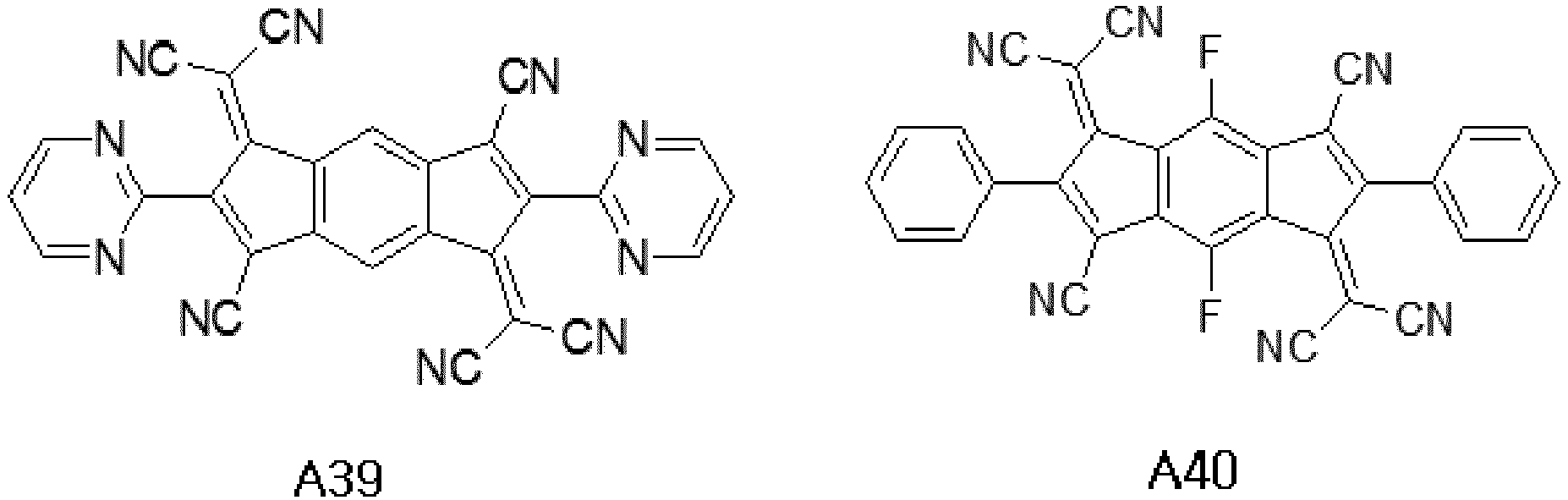


- The compound represented by the above Chemical Formula 2 preferably is one among the following compounds:


- The at least one organic layer preferably includes a hole injection layer.
- A dopant of the hole injection layer preferably includes the compound.
- The hole injection layer preferably includes the compound.
- The at least one organic layer preferably includes a P-type charge generation layer.
- A dopant of the P-type charge generation layer preferably includes the compound.
- The P-type charge generation layer preferably includes the compound.
- In another aspect of the disclosure, an organic light emitting display device comprises at least one light emitting part between an anode and a cathode, and the at least one light emitting part having a hole injection layer and a light emitting layer, and a charge generation layer having a P-type charge generation layer between the light emitting parts, wherein at least one among the hole injection layer and the P-type charge generation layer comprises a compound represented by the following Chemical Formula 1 or 2:


- Z1 and Z2 are independently represented by the following Chemical Formula 3:

- The substituent of the aryl group, heteroaryl group, alkyl group, alkoxy group, and ether group is one among an alkyl with 1 to 12 carbon atoms, an aryl with 6 to 15 carbon atoms, a hetero alkyl with 1 to 15 carbon atoms and 1 to 4 heteroatoms one among O, N, S, and Si" a cyano group, a fluorine group, a trifluoromethyl group, a trifluoromethoxy group, and a trimethylsilyl group.
- The compound represented by Chemical Formula 1 includes one among the following compounds:


- The compound represented by the above Chemical Formula 2 preferably includes one among the following compounds:


- A dopant for the hole injection layer preferably includes the compound.
- The hole injection layer preferably includes the compound.
- A dopant for the P-type charge generation layer preferably includes the compound.
- The P-type charge generation layer preferably includes the compound.
- The accompanying drawings, which are included to provide a further understanding of the disclosure and are incorporated in and constitute a part of this specification, illustrate embodiments of the disclosure and together with the description serve to explain the principles of the disclosure.
-
FIG. 1 is a cross-sectional view showing an organic light emitting display device according to a first exemplary embodiment of the present disclosure; -
FIG. 2 is a cross-sectional view showing an organic light emitting display device according to a second exemplary embodiment of the present disclosure; -
FIG. 3 is a cross-sectional view showing an organic light emitting display device according to a third exemplary embodiment of the present disclosure; and -
FIGS. 4 and 5 are energy band diagrams of an organic light emitting display device according to one or more embodiments of the present disclosure. - The advantages and features of the present disclosure and methods for accomplishing the same may be understood more readily by reference to the following detailed descriptions of exemplary embodiments and the accompanying drawings. The present disclosure may, however, be embodied in many different forms and should not be construed as being limited to the exemplary embodiments set forth herein. Rather, these exemplary embodiments are provided so that this disclosure will be thorough and complete and will fully convey the concept of the present disclosure to those skilled in the art, and the present disclosure is defined by the appended claims
- The shapes, sizes, percentages, angles, numbers, etc shown in the figures to describe the exemplary embodiments of the present disclosure are merely examples and not limited to those shown in the figures. Like reference numerals denote like elements throughout the specification. In describing the present disclosure, detailed descriptions of related well-known technologies will be omitted to avoid unnecessary obscuring the present disclosure. When the terms 'comprise', 'have', 'consist of' and the like are used, other parts may be added as long as the term 'only' is not used. The singular forms may be interpreted as the plural forms unless explicitly stated.
- The elements may be interpreted to include an error margin even if not explicitly stated.
- When the position relation between two parts is described using the terms 'on', 'over', 'under', 'next to' and the like, one or more parts may be positioned between the two parts as long as the term 'immediately' or 'directly' is not used.
- When the temporal relationship between two events is described using the terms 'after', 'following', 'next', 'before' and the like, the two events may not occur in succession as long as the term 'immediately' or 'directly' is not used.
- It will be understood that, although the terms first, second, etc., may be used to describe various elements, these elements should not be limited by these terms. These terms are only used to distinguish one element from another element. Thus, a first element discussed below could be termed a second element without departing from the technical spirit of the present disclosure.
- The features of various exemplary embodiments of the present disclosure may be combined with one another either partly or wholly, and may technically interact or work together in various ways. The exemplary embodiments may be carried out independently or in combination with one another.
- Hereinafter, various exemplary embodiments of the present disclosure will be described in detail with reference to the accompanying drawings.
-
FIG. 1 is a cross-sectional view showing an organic light emitting display device according to a first exemplary embodiment of the present disclosure. All the components of the organic light emitting display device according to all embodiments of the present disclosure are operatively coupled and configured. - Referring to
FIG. 1 , an organic light emittingdisplay device 100 according to the first exemplary embodiment of the present disclosure comprises ananode 110, ahole injection layer 120, ahole transport layer 130, anlight emitting layer 140, anelectron transport layer 150, anelectron injection layer 210, and acathode 220. - The
anode 110 is a hole injection electrode, and may be formed of one among ITO (indium tin oxide), IZO (indium zinc oxide), or ZnO (zinc oxide) having a high work function. Also, if theanode 110 is a reflective electrode, theanode 110 may further comprise a reflective layer formed of one among aluminum (Al), silver (Ag), or nickel (Ni) under a layer formed of one among ITO, IZO, or ZnO. - The
hole injection layer 120 is formed on theanode 110. Thehole injection layer 120 has to comprise a strong electron-attracting substituent, in order to make the LUMO energy level of the hole injection layer similar to or lower than the HOMO energy level of the host of the hole injection layer or the HOMO energy level of the hole transport layer. However, compounds comprising an electron-attracting substituent are hard to synthesize because of the electron-attracting substituents, and are not easy to develop due to their low thermal and deposition stability. In view of this, the present inventors conducted various tests to improve the hole injection properties and the device's efficiency and lifetime by forming a hole injection layer of a material that ensures process stability and comprises an electron-attracting substituent. - Through a number of tests or experiments which were performed on materials that do not affect the lifetime or efficiency of the organic light emitting display device and that cause no rise in operating voltage, the present inventors developed compounds that can exhibit hole injection properties by ensuring process stability and comprising an electron-attracting substituent. In the present disclosure, a hole injection layer is formed using a compound comprising indene as a core and an electron-attracting substituent. The composition and deposition of the compound is simplified because indene provides process stability against heat or deposition. Moreover, the compound of this disclosure can improve the hole injection properties by comprising an electron-attracting substituent attached to the core and making the LUMO energy level of the compound similar to or lower than the HOMO energy level of the host of the
hole injection layer 120, the host of a P-type charge generation layer, or the hole transport layer. - Accordingly, the
hole injection layer 120 of this disclosure comprises a compound represented by the following Chemical Formula 1 or 2:

- where R1 to R6 each independently represents one among a hydrogen atom, a substituted or unsubstituted aryl group with 6 to 12 carbon atoms, a substituted or unsubstituted heteroaryl group with 1 to 12 carbon atoms and 1 to 4 heteroatoms one among O, N, S, and Si, a substituted or unsubstituted alkyl group with 1 to 12 carbon atoms, a substituted or unsubstituted alkoxy group with 1 to 12 carbon atoms, a substituted or unsubstituted ether group with 1 to 12 carbon atoms, a cyano group, a fluorine group, a trifluoromethyl group, a trifluoromethoxy group, and a trimethylsilyl group, and at least one among R1 to R6 comprises a cyano group.
- Z1 and Z2 include independently represented by the following Chemical Formula 3:

- The substituent of the aryl group, heteroaryl group, alkyl group, alkoxy group, and ether group may be one among an alkyl with 1 to 12 carbon atoms, an aryl with 6 to 15 carbon atoms, a hetero alkyl with 1 to 15 carbon atoms and 1 to 4 heteroatoms one among O, N, S, and Si, a cyano group, a fluorine group, a trifluoromethyl group, a trifluoromethoxy group, and a trimethylsilyl group.
- The compound represented by Chemical Formula 1 includes one among the following compounds:


- The compound represented by the above Chemical Formula 2 includes one among the following compounds:


- The above-described compound of this disclosure comprises indene as a core, which provides process stability against heat or deposition, thus simplifying the composition and deposition of the compound. Moreover, the compound of this disclosure improves the hole injection properties by comprising an electron-attracting substituent attached to the core and making the LUMO energy level of the compound similar to or lower than the HOMO energy level of the host of the hole injection layer, the host of the P-type charge generation layer, or the hole transport layer.
- Accordingly, the hole injection layer is formed of the compound of this disclosure to ensure the process stability of the compound, simplifying the fabrication of the organic light emitting display device. Moreover, the compound of this disclosure can reduce the device's operating voltage and improve its efficiency and lifetime since the improvement in hole injection properties helps to facilitate the transfer of holes from the anode to the light emitting layer.
- The
hole injection layer 120 may be formed of a compound of this disclosure, or may comprise the compound as a dopant. Thehole injection layer 120 may form solely of a compound of this disclosure. Also, if thehole injection layer 120 comprises a compound of this disclosure as a dopant, thehole injection layer 120 may comprise one or more hosts among CuPc(copper phthalocyanine), PEDOT(poly(3,4)-ethylenedioxythiophene), PANI(polyaniline), DNTPD(N1',N1 "-(biphenyl-4,4'-diyl)bis(N'-phenyl-N4,N4-di-m-tolylbenzene-1,4-diamine), and NPD(N,N'-bis(naphthalene-1-yl)-N,N'-bis(phenyl)-2,2'-dimethylbenzidine) and a dopant comprising the compound of this disclosure. - The
hole injection layer 120 may have a 1 to 150 nm thickness. If thehole injection layer 120 has a 1 nm thickness or greater, the hole injection properties may be improved. If thehole injection layer 120 has a 150 nm thickness or less, an increase in the thickness of thehole injection layer 120 may be prevented and a rise in operating voltage may be therefore prevented. - The
hole transport layer 130 may function to facilitate hole transport, and may be formed of, but is not limited to, one or more among NPD(N,N'-bis(naphthalene-1-yl)-N,N'-bis(phenyl)-2,2'-dimethylbenzidine), TPD(N,N'-bis-(3-methylphenyl)-N,N'-bis(phenyl)-benzidine), spiro-TAD(2,2'7,7'-tetrakis(N,N-diphenylamino)-9,9'-spirofluorene), NPB(N,N'-bis(naphthalene-1-yl-N,N'-bis(phenyl)-benzidine), and MTDATA(4,4',4"-Tris(N-3-methylphenyl-N-phenylamino)-triphenylamine). Thehole transport layer 130 may have a 1 to 150 nm thickness. If thehole transport layer 130 has a 1 nm thickness or greater, the hole transport properties may be improved, or if thehole transport layer 130 has a 150 nm thickness or less, an increase in the thickness of thehole transport layer 130 may be prevented, and a rise in operating voltage may be therefore prevented. Moreover, an electron blocking layer may be further formed over thehole transport layer 130. - The
light emitting layer 140 may emit light of red (R), green (G), or blue (B), and may be formed of a fluorescent material or phosphorescent material. - If the
light emitting layer 140 is a red light emitting layer, it may be formed of, but is not limited to, a fluorescent material comprising PBD:Eu(DBM)3(Phen) or perylene. If thelight emitting layer 140 is a green light emitting layer, it may be formed of, but is not limited to, a fluorescent material comprising Alq3(tris(8-hydroxyquinolinato)aluminum). If thelight emitting layer 140 is a blue light emitting layer, it may be formed of, but is not limited to, a fluorescent material comprising one among spiro-BDAVBi(2,7-bis[4-(diphenylamino)styryl]-9,9-spirofluorene), spiro-CBP(2,2',7,7'-tetrakis(carbozol-9-yl)-9,9-spirofluorene), distyrylbenzene (DSB), distyrylarylene (DSA), a PFO (polyfluorene) polymer, and a PPV(polyphenylenevinylene) polymer. - The
electron transport layer 150 may function to facilitate the transport of electrons, and may be formed of, but is not limited to, one or more among Alq3(tris(8-hydroxyquinolinato)aluminum), PBD(2-4-biphenyl)-5-(4-tert-butylphenyl)-1,3,4-oxadiazole), TAZ(3-(4-biphenyl)-4-pheynyl-5-tert-butylphenyl-1,2,4-triazole), DPT(2-biphenyl-4-yl-4,6-bis-(4 '-pyridin-2-yl-biphenyl-4-yl)-[1,3,5]triazine), and BAlq(Bis(2-methyl-8-quinolinolato)-4-(phenylphenolato)aluminum). Theelectron transport layer 150 may have a 1 to 150 nm thickness. If theelectron transport layer 150 has a 1 nm thickness or greater, a degradation of the electron transport properties may be prevented, or if theelectron transport layer 150 has a 150 nm thickness or less, an increase in the thickness of theelectron transport layer 150 may be prevented, and a rise in operating voltage may be therefore prevented. - The
electron injection layer 210 functions to facilitate electron injection, and may be formed of, but is not limited to, one among Alq3(tris(8-hydroxyquinolinato)aluminum), PBD(2-4-biphenyl)-5-(4-tert-butylphenyl)-1,3,4-oxadiazole), TAZ(3-(4-biphenyl)-4-pheynyl-5-tert-butylphenyl-1,2,4-triazole), and BAlq(Bis(2-methyl-8-quinolinolato)-4-(phenylphenolato)aluminum). On the other hand, theelectron injection layer 210 may be formed of a metal compound, and the metal compound may be, for example, but is not limited to, one or more among LiQ, LiF, NaF, KF, RbF, CsF, FrF, BeF2, MgF2, CaF2, SrF2, BaF2, and RaF2. Theelectron injection layer 210 may have a 1 to 50 nm thickness. If theelectron injection layer 210 has a 1 nm thickness or greater, a degradation of the electron injection properties may be prevented. If theelectron injection layer 210 has a 50 nm thickness or less, an increase in the thickness of theelectron injection layer 210 may be prevented, and a rise in operating voltage may be therefore prevented. Theelectron injection layer 210 may not be included in the elements of the organic light emitting display device, depending on the structure or characteristics of the device. - The
cathode 220 is an electron injection electrode, and may be formed of magnesium (Mg), calcium (Ca), aluminum (Al), silver (Ag), or an alloy thereof, having a low work function. If the organic light emitting display device is a top-emission type or a dual-emission type, thecathode 220 may be formed thin enough to pass light therethrough. If the organic light emitting display device is a bottom-emission type, thecathode 220 may be formed thick enough to reflect light. - As above, a compound of this disclosure comprises indene as a core, which provides process stability against heat or deposition, thus simplifying the composition and deposition of the compound. Moreover, the compound of this disclosure improves the hole injection properties by comprising an electron-attracting substituent attached to the core and making the LUMO energy level of the compound similar to or lower than the HOMO energy level of the host of the hole injection layer, the host of the P-type charge generation layer, or the hole transport layer.
- Accordingly, the hole injection layer is formed of the compound of this disclosure to ensure the process stability of the compound, which simplifies the fabrication of the organic light emitting display device. Moreover, the compound of this disclosure can reduce the device's operating voltage and improve its efficiency and lifetime since the improvement in hole injection properties helps to facilitate the transfer of holes from the anode to the light emitting layer.
-
FIG. 2 is a view showing an organic light emitting display device according to a second exemplary embodiment of the present disclosure. The same elements as the first exemplary embodiment are denoted by the same reference numerals, so descriptions of these elements will be omitted or may be brief below. - Referring to
FIG. 2 , an organic light emittingdisplay device 100 of the present disclosure comprises light emitting parts ST1 and ST2 between ananode 110 and acathode 220, and acharge generation layer 160 between the light emitting parts ST1 and ST2. - The first light emitting part ST1 comprises a first
light emitting layer 140. The firstlight emitting layer 140 may emit light of red (R), green (G), or blue (B), and may be formed of a fluorescent or phosphorescent material. In this exemplary embodiment, the firstlight emitting layer 140 may be a blue light emitting layer. The blue light emitting layer comprises one among a blue light emitting layer, a dark blue light emitting layer, and a sky blue light emitting layer. Alternatively, the firstlight emitting layer 140 may form of a blue light emitting layer and a red light emitting layer, a blue light emitting layer and a yellow-green light emitting layer, or a blue light emitting layer and a green light emitting layer. If the firstlight emitting layer 140 is a blue light emitting layer, it may emit light over a wavelength range of 440 to 480 nm. If the firstlight emitting layer 140 forms of a blue light emitting layer and a red light emitting layer, it may emit light over a wavelength range of 440 to 650 nm. If the firstlight emitting layer 140 forms of a blue light emitting layer and a yellow-green light emitting layer, it may emit light over a wavelength range of 440 to 590 nm. If the firstlight emitting layer 140 forms of a blue light emitting layer and a green light emitting layer, it may emit light over a wavelength range of 440 to 580 nm. - The first light emitting part ST1 comprises a
hole injection layer 120 and a firsthole transport layer 130 that are between theanode 110 and the firstlight emitting layer 140, and a firstelectron transport layer 150 on the firstlight emitting layer 140. Accordingly, the first light emitting part ST1 comprising thehole injection layer 120, firsthole transport layer 130, firstlight emitting layer 140, and firstelectron transport layer 150 is formed on theanode 110. The firsthole transport layer 130 may be formed of, but is not limited to, the same material as thehole transport layer 130 explained with reference toFIG. 1 . - A charge generation layer (CGL) 160 is between the first light emitting part ST1 and the second light emitting part ST2. The first light emitting part ST1 and the second light emitting part ST2 are connected by the
charge generation layer 160. Thecharge generation layer 160 may be a PN-junction charge generation layer formed by joining an N-typecharge generation layer 160N and a P-typecharge generation layer 160P. The PN junctioncharge generation layer 160 generates a charge, or injects the charge (i.e., electrons and holes), separately into the light emitting layer. That is, the N-typecharge generation layer 160N transfers electrons to the firstelectron transport layer 150, and the firstelectron transport layer 150 supplies the electrons to the firstlight emitting layer 140 adjacent to the anode. The P-typecharge generation layer 160P transfers holes to the secondhole transport layer 180, and the secondhole transport layer 180 supplies the holes to the secondlight emitting layer 190 of the second light emitting part ST2. As such, the luminous efficiency of the first and secondlight emitting layers - The N-type
charge generation layer 160N may be formed of a metal or an N-doped organic material. The metal may be one among Li, Na, K, Rb, Cs, Mg, Ca, Sr, Ba, La, Ce, Sm, Eu, Tb, Dy, and Yb. An N-type dopant and host for the N-doped organic material may be commonly-used materials. For example, the N-type dopant may be an alkali metal, an alkali metal compound, an alkali earth metal, or an alkali earth metal compound. Specifically, the N-type dopant may be one among Li, Cs, K, Rb, Mg, Na, Ca, Sr, Eu, and Yb. The host material may be an organic matter that has a nitrogen atom-containing hetero ring, with 20 to 60 carbon atoms, for example, one material among Alq3(tris(8-hydroxyquinolinato)aluminum), triazine, a hydroxyquinoline derivative, a benzazole derivative, and a silole derivative. - The P-type
charge generation layer 160P may be formed of the same material as thehole injection layer 120 of the above-described first exemplary embodiment. A compound of this disclosure comprises indene as a core, which provides process stability against heat or deposition, thus simplifying the composition and deposition of the compound. Moreover, the compound of this disclosure improves the hole injection properties by comprising an electron-attracting substituent attached to the core and making the LUMO energy level of the compound similar to or lower than the HOMO energy level of the hole transport layer. - Accordingly, the P-type charge generation layer is formed of the compound of this disclosure to ensure the process stability of the compound, which simplifies the fabrication of the organic light emitting display device. Moreover, the compound of this disclosure can reduce the device's operating voltage and improve its efficiency and lifetime since the improvement in hole injection properties helps to facilitate the transfer of holes from the anode to the light emitting layer.
- The second light emitting part ST2 comprising a second
hole transport layer 180, the secondlight emitting layer 190, a secondelectron transport layer 200, and anelectron injection layer 210 is on thecharge generation layer 160. - The second
light emitting layer 190 may emit light of red (R), green (G), blue (B), or yellow-green (YG), and may be formed of a fluorescent or phosphorescent material. In this exemplary embodiment, the secondlight emitting layer 190 may be a light emitting layer that emits yellow-green light. The secondlight emitting layer 190 may have a single layer structure of a yellow-green light emitting layer or a green light emitting layer, or a multilayer structure formed of a yellow-green light emitting layer and a green light emitting layer. The secondlight emitting layer 190 comprises a yellow-green light emitting layer, a green light emitting layer, or a multilayer structure formed of a yellow-green light emitting layer and a green light emitting layer, a yellow light emitting layer and a red light emitting layer, a green light emitting layer and a red light emitting layer, or a yellow-green light emitting layer and a red light emitting layer. If the secondlight emitting layer 190 forms of a yellow-green light emitting layer, a green light emitting layer, or a yellow-green light emitting layer and a green light emitting layer, it may emit light over a wavelength range of 510 to 590 nm. If the secondlight emitting layer 190 is formed of a yellow light emitting layer and a red light emitting layer, a green light emitting layer and a red light emitting layer, or a yellow-green light emitting layer and a red light emitting layer, it may emit light over a wavelength range of 510 to 650 nm. - This exemplary embodiment will be described by taking as an example a single layer structure of a second
light emitting layer 190 that emits yellow-green light. The secondlight emitting layer 190 may comprise, but is not limited to, at least one host of CBP (4,4'-bis(carbazol-9-yl)biphenyl) and BAlq(Bis(2-methyl-8-quinolinolato)-4-(phenylphenolato)aluminum) and a phosphorescent yellow-green dopant that emits yellow-green light. - The second light emitting part ST2 comprises the second
hole transport layer 180 between thecharge generation layer 160 and the secondlight emitting layer 190, and comprises the secondelectron transport layer 200 andelectron injection layer 210 on the secondlight emitting layer 190. The secondhole transport layer 180 may be formed of, but is not limited to, the same material as thehole transport layer 130 explained with reference toFIG. 1 . - Accordingly, the second light emitting part ST2 comprising the second
hole transport layer 180, secondlight emitting layer 190, secondelectron transport layer 200, andelectron injection layer 210 is formed on thecharge generation layer 160. Thecathode 220 is provided on the second light emitting part ST2 to constitute the organic light emitting display device according to the second exemplary embodiment of the present disclosure. - The above-described second exemplary embodiment of the present disclosure has disclosed that the P-type
charge generation layer 160P comprise a compound of this disclosure. As in the above-described first exemplary embodiment, the compound of this disclosure may be also used as thehole injection layer 120. The compound of this disclosure may be included in at least one among thehole injection layer 120 and the P-typecharge generation layer 160P. - As above, a compound of this disclosure comprises indene as a core, which provides process stability against heat or deposition, thus simplifying the composition and deposition of the compound. Moreover, the compound of this disclosure can improve the hole injection properties by comprising an electron-attracting substituent attached to the core and making the LUMO energy level of the compound similar to or lower than the HOMO energy level of host of the hole injection layer, the host of the P-type charge generation layer, or the hole transport layer.
- Accordingly, at least one among the hole injection layer and the P-type charge generation layer is formed of the compound of this disclosure to ensure the process stability of the compound, which simplifies the fabrication of the organic light emitting display device. Moreover, the compound of this disclosure can reduce the device's operating voltage and improve its efficiency and lifetime since the improvement in hole injection properties helps to facilitate the transfer of holes from the anode to the light emitting layer.
-
FIG. 3 is a view showing an organic light emitting display device according to a third exemplary embodiment of the present disclosure. The same elements as the first and second exemplary embodiments are denoted by the same reference numerals, so descriptions of these elements will be omitted or may be brief below. - Referring to
FIG. 3 , an organic light emittingdisplay device 100 of the present disclosure comprises a plurality of light emitting parts ST1, ST2, and ST3 between ananode 110 and acathode 220, and a firstcharge generation layer 160 and a secondcharge generation layer 230 that are between the light emitting parts ST1, ST2, and ST3. Although this exemplary embodiment has been illustrated and described with an example where three light emitting parts are between theanode 110 and thecathode 220, the present disclosure is not limited to this example and four or more light emitting parts may be between theanode 110 and thecathode 220. - Among the light emitting parts, the first light emitting part ST1 comprises a first
light emitting layer 140. The firstlight emitting layer 140 may emit light one among red, green, and blue. For example, it may be a blue light emitting layer in this exemplary embodiment. The blue light emitting layer comprises one among a blue light emitting layer, a dark blue light emitting layer, and a sky blue light emitting layer. Alternatively, the firstlight emitting layer 140 may form of a blue light emitting layer and a red light emitting layer, a blue light emitting layer and a yellow-green light emitting layer, or a blue light emitting layer and a green light emitting layer. If the firstlight emitting layer 140 is a blue light emitting layer, it may emit light over a wavelength range of 440 to 480 nm. If the firstlight emitting layer 140 forms of a blue light emitting layer and a red light emitting layer, it may emit light over a wavelength range of 440 to 650 nm. If the firstlight emitting layer 140 forms of a blue light emitting layer and a yellow-green light emitting layer, it may emit light over a wavelength range of 440 to 590 nm. If the firstlight emitting layer 140 forms of a blue light emitting layer and a green light emitting layer, it may emit light over a wavelength range of 440 to 580 nm. - The first light emitting part ST1 comprises a
hole injection layer 120 and a firsthole transport layer 130 that are between theanode 110 and the firstlight emitting layer 140, and a firstelectron transport layer 150 on the firstlight emitting layer 140. Accordingly, the first light emitting part ST1 comprising thehole injection layer 120, the firsthole transport layer 130, the firstlight emitting layer 140, and the firstelectron transport layer 150 is formed on theanode 110. - The second light emitting part ST2 comprising a second
light emitting layer 190 is on the first light emitting part ST1. The secondlight emitting layer 190 may emit light of one among red, green, blue, and yellow-green. For example, it may be a yellow-green light emitting layer in this exemplary embodiment. The secondlight emitting layer 190 comprises a yellow-green light emitting layer, a green light emitting layer, or a multilayer structure formed of a yellow-green light emitting layer and a green light emitting layer, a yellow light emitting layer and a red light emitting layer, a green light emitting layer and a red light emitting layer, or a yellow-green light emitting layer and a red light emitting layer. If the secondlight emitting layer 190 forms of a yellow-green light emitting layer, a green light emitting layer, or a yellow-green light emitting layer and a green light emitting layer, it may emit light over a wavelength range of 510 to 590 nm. If the secondlight emitting layer 190 forms of a yellow light emitting layer and a red light emitting layer, a green light emitting layer and a red light emitting layer, or a yellow-green light emitting layer and a red light emitting layer, it may emit light over a wavelength range of 510 to 650 nm. - The second light emitting part ST2 further comprises a second
hole transport layer 180 on the first light emitting part ST1, and comprises a secondelectron transport layer 200 on the secondlight emitting layer 190. Accordingly, the second light emitting part ST2 comprising the secondhole transport layer 180, the secondlight emitting layer 190, and the secondelectron transport layer 200 is formed on the first light emitting part ST1. - A first
charge generation layer 160 is between the first light emitting part ST1 and the second light emitting part ST2. The firstcharge generation layer 160 is a PN-junction charge generation layer formed by joining an N-typecharge generation layer 160N and a P-typecharge generation layer 160P. The firstcharge generation layer 160 generates a charge, or injects the charge, i.e., electrons and holes, separately into the first and secondlight emitting layers - The third light emitting part ST3 comprising a third
light emitting layer 250 is on the second light emitting part ST2. The thirdlight emitting layer 250 may emit light one among red, green, and blue, and be formed of a fluorescent material. For example, it may be a blue light emitting layer in this exemplary embodiment. The blue light emitting layer comprises one among a blue light emitting layer, a dark blue light emitting layer, and a sky blue light emitting layer. Alternatively, the thirdlight emitting layer 250 may form of a blue light emitting layer and a red light emitting layer, a blue light emitting layer and a yellow-green light emitting layer, or a blue light emitting layer and a green light emitting layer. If the thirdlight emitting layer 250 is a blue light emitting layer, it may emit light over a wavelength range of 440 to 480 nm. If the thirdlight emitting layer 250 forms of a blue light emitting layer and a red light emitting layer, it may emit light over a wavelength range of 440 to 650 nm. If the thirdlight emitting layer 250 forms of a blue light emitting layer and a yellow-green light emitting layer, it may emit light over a wavelength range of 440 to 590 nm. If the thirdlight emitting layer 250 forms of a blue light emitting layer and a green light emitting layer, it may emit light over a wavelength range of 440 to 580 nm. - The third light emitting part ST3 further comprises a third
hole transport layer 240 on the second light emitting part ST2, and a thirdelectron transport layer 260 and anelectron injection layer 210 that are on the thirdlight emitting layer 250. Accordingly, the third light emitting part ST3 comprising the thirdhole transport layer 240, thirdlight emitting layer 250, thirdelectron transport layer 260, andelectron injection layer 210 is formed on the second light emitting part ST2. Theelectron injection layer 210 may not be included in the elements of the third light emitting part ST3, depending on the structure or characteristics of the device. - The second
charge generation layer 230 is between the second light emitting part ST2 and the third light emitting part ST3. The secondcharge generation layer 230 is a PN junction charge generation layer formed by joining the N-typecharge generation layer 230N and the P-typecharge generation layer 230P. The secondcharge generation layer 230 generates a charge, or injects the charge, i.e., electrons and holes, separately into the second and thirdlight emitting layers cathode 220 is provided on the third light emitting part ST3 to constitute the organic light emitting display device according to the third exemplary embodiment of the present disclosure. - At least one among the
hole injection layer 120, the P-typecharge generation layer 160P of the firstcharge generation layer 160, and the P-type charge generation layer 260P of the secondcharge generation layer 260 is formed of a compound of this disclosure, as in the case of the foregoing exemplary embodiments. A compound of this disclosure comprises indene as a core, which provides process stability against heat or deposition, thus simplifying the composition and deposition of the compound. Moreover, the compound of this disclosure improves the hole injection properties by comprising an electron-attracting substituent attached to the core and making the LUMO energy level of the compound similar to or lower than the HOMO energy level of host of the hole injection layer, the host of the P-type charge generation layer, or the hole transport layer. - Accordingly, at least one among the hole injection layer and the P-type charge generation layer is formed of the compound of this disclosure to ensure the process stability of the compound, which simplifies the fabrication of the organic light emitting display device. Moreover, the compound of this disclosure can reduce the device's operating voltage and improve its efficiency and lifetime since the improvement in hole injection properties helps to facilitate the transfer of holes from the anode to the light emitting layer.
- Organic light emitting displays using the organic light emitting display device according to the first to third exemplary embodiments of the present disclosure may include top emission displays, bottom emission displays, dual emission displays, and vehicle lighting. The vehicle lighting may include, but are not necessarily limited to, headlights, high beams, taillights, brake lights, and back-up lights. Moreover, organic light emitting displays using the organic light emitting display devices according to the first to third exemplary embodiments of the present disclosure may be applied to mobile devices, tablet PCs, monitors, smartwatches, laptop computers, vehicle displays, etc. Besides, these organic light emitting displays may be applied to vehicle displays, wearable displays, foldable displays, rollable displays, etc.
- Also, organic light emitting displays using the organic light emitting display device according to the second exemplary embodiment of the present disclosure may be applied to displays in which the first and second light emitting layers emit light of the same color.
- Also, organic light emitting displays using the organic light emitting display device according to the third exemplary embodiment of the present disclosure may be applied to displays in which at least two of the first, second, and third light emitting layers emit light of the same color.
-
FIGS. 4 and 5 are energy band diagrams of an organic light emitting display device of the present disclosure. Referring toFIG. 4 , theanode 110, thehole injection layer 120, thehole transport layer 130, and thelight emitting layer 140 are illustrated. Thehole injection layer 120 may be formed of a single material comprising a compound of this disclosure. Thehole transport layer 130 may be formed of, for example, NPD. Since the LUMO energy level of the compound in thehole injection layer 120 is similar to or lower than the HOMO energy level of thehole transport layer 130, electrons are accepted from the HOMO energy level of thehole transport layer 130 to the LUMO energy level of the compound, thereby forming a hole transport path. Accordingly, holes can be smoothly injected from thehole injection layer 120 into thehole transport layer 130 through the hole transport path (indicated by the arrows) between thehole injection layer 120 and thehole transport layer 130. - Referring to
FIG. 5 , thehole injection layer 120 may comprise a dopant introduced into a host. Accordingly, a compound of this disclosure acts as the dopant. Since the LUMO energy level of the compound used as a dopant for thehole injection layer 120 is similar to or lower than the HOMO energy level of the host, electrons are accepted from the HOMO energy level of the host to the LUMO energy level of the compound of this disclosure, thereby forming a hole transport path (indicated by the arrow). Accordingly, holes can be smoothly injected from thehole injection layer 120 into thehole transport layer 130 through the hole transport path between the HOMO energy level of the host and the LUMO energy level of the compound of this disclosure, within thehole injection layer 120. As a result, the use of the compound of this disclosure as a dopant for thehole injection layer 120 facilitates the transfer of holes from thehole injection layer 120 into thehole transport layer 130, leading to a reduction in operating voltage. - Although
FIGS. 4 and 5 are explained with respect to the hole injection layer by way of example, the same may apply when thehole injection layer 120 is replaced with the P-typecharge generation layer 160P ofFIG. 2 and thehole transport layer 130 is replaced with the second hole transport layer 170 ofFIG. 2 . Accordingly, referring toFIG. 4 , if thehole injection layer 120 is replaced with the P-typecharge generation layer 160P ofFIG. 2 , the P-typecharge generation layer 160P may be formed of a single material comprising a compound of this disclosure. Also, referring toFIG. 5 , the P-typecharge generation layer 160P may comprise a compound of this disclosure as a dopant. - Moreover, the same applies when the
hole injection layer 120 is replaced with the P-typecharge generation layer 160P ofFIG. 3 and thehole transport layer 130 is replaced with the second hole transport layer 170 ofFIG. 3 . Accordingly, referring toFIG. 4 , if thehole injection layer 120 is replaced with the P-typecharge generation layer 160P ofFIG. 3 , the P-typecharge generation layer 160P may be formed of a single material comprising a compound of this disclosure. Also, referring toFIG. 5 , the P-typecharge generation layer 160P may comprise a compound of this disclosure as a dopant. - Furthermore, the same applies when the
hole injection layer 120 is replaced with the P-typecharge generation layer 230P ofFIG. 3 and thehole transport layer 130 is replaced with the thirdhole transport layer 240 ofFIG. 3 . Accordingly, referring toFIG. 4 , if thehole injection layer 120 is replaced with the P-typecharge generation layer 230P ofFIG. 3 , the P-typecharge generation layer 230P may be formed of a single material comprising a compound of this disclosure. Also, referring toFIG. 5 , the P-typecharge generation layer 230P may comprise a compound of this disclosure as a dopant. - Hereinafter, synthesis examples of compounds of the present disclosure will be described in detail. However, the following examples are only for illustration, and the present disclosure is not limited thereto.
-


- 2-bromophenyl)acetonitrile (0.12 mol), bis(triphenylphosphine)palladium(II)chloride (PdCl2(PPh3)2) (2 mmol), copper iodide (Cul) (2 mmol), triphenylphosphine (PPh3) (4 mmol), and diisopropylamine (i-Pr2NH) (0.1 mol) were put into a 250 ml two-necked flask under a nitrogen atmosphere and stirred for 5 min at room temperature, and then 1,5-dibromophenyl-2,4-dicarbonitrile (0.05 mol) was added to the mixture and stirred for 24 hours at 50°C. An organic layer was obtained by extraction with H2O/ethyl acetate, dried over magnesium sulfate (MgSO4), and then subjected to column chromatography to give 10.9 g of solid (yield: 61 %).
-

- 1,5-bis(chloromethyl)-2,4-bis(2-phenylethynyl)benzene (0.03 mol), palladium(II) chloride (PdCl2) (6.1 mmol), silver hexafluoroantimonate (AgSbF6) (9.1 mmol), and diphenylsulfoxide (Ph2SO) (0.18 mol) were dissolved in a 250 ml two-necked flask with dichloroethylene (DCE) and stirred for 24 hours at 60 °C, and then cesium carbonate (Cs2CO3) (0.074 mol) was added to the mixture and stirred for 12 hours. After the reaction, an extract was obtained by extraction with dichloromethane (CH2Cl2), which was dried up after the extraction, and then put into 35 % hydrochloric acid (HCl) and stirred for 2 hours. An organic layer was obtained by extraction with a dichloromethane/ammonium chloride (CH2Cl2/aq.NH4Cl) solution, dried over magnesium sulfate (MgSO4), and then subjected to column chromatography to give 4.4 g of solid (yield: 38 %).
-

- 3,5-dihydro-3,5-dioxo-2,6-diphenyl-s-indacene-1,7-dicarbonitrile (0.01 mol), malononitrile (0.062 mol), and dichloromethane (CH2Cl2) were put into a 100 ml two-necked flask and stirred for 30 min under an argon atmosphere. Titanium(IV) chloride (TiCl4) (0.062 mol) was slowly added to the mixture, followed by the addition of pyridine (0.1 mol), and stirred at room temperature. An organic layer was obtained by extraction with a dichloromethane/ammonium chloride (CH2Cl2/aq.NH4Cl) solution, dried over magnesium sulfate (MgSO4), and then subjected to column chromatography to give 1.6 g of solid, i.e., Compound B31 (yield: 32 %).
-


- 4-ethynylbenzonitrile (0.12 mol), bis(triphenylphosphine)palladium(II)chloride (PdCl2(PPh3)2) (2 mmol), copper iodide (Cul) (2 mmol), triphenylphosphine (PPh3) (4 mmol), and diisopropylamine (i-Pr2NH) (0.1 mol) were put into a 250 ml two-necked flask under a nitrogen atmosphere and stirred for 5 min at room temperature, and then 1,4-dibromo-2,5-di(cyanomethyl)benzene (0.05 mol) was added to the mixture and stirred for 24 hours at 50 °C. An organic layer was obtained by extraction with H2O/ethyl acetate, dried over magnesium sulfate (MgSO4), and then subjected to column chromatography to give 13.8 g of solid (yield: 68 %).
-

- 1,4-di(cyanomethyl)-2,5-bis(2-(4-cyanophenyl)ethynyl)benzene (0.034 mol), palladium(II)chloride (PdCl2) (6.8 mmol), silver hexafluoroantimonate (AgSbF6) (10.2 mmol), and diphenylsulfoxide (Ph2SO) (0.2 mol) were dissolved in a 250 ml two-necked flask with dichloroethylene (DCE) and stirred for 24 hours at 60 °C. After the reaction, an extract was obtained by extraction with dichloromethane (CH2Cl2), which was dried up after the extraction, and then put into 35 % hydrochloric acid (HCl) and stirred for 2 hours. An organic layer was obtained by extraction with a dichloromethane/ammonium chloride (CH2Cl2/aq.NH4Cl) solution, dried over magnesium sulfate (MgSO4), and then subjected to column chromatography to give 5.9 g of solid, i.e., an intermediate, (yield: 48 %).
-

- 2,6-bis(4-cyanophenyl)-3,7-dihydro-3,7-dioxo-s-indacene-1,5-dicarbonitrile (13.6 mmol), malononitrile (0.082 mol), and dichloromethane (CH2Cl2) were put into a 100 ml two-necked flask and stirred for 30 min under an argon atmosphere. Titanium(IV)chloride (TiCl4) (0.082 mol) was slowly added to the mixture, followed by the addition of pyridine (0.1 mol), and stirred at room temperature. After the reaction, an organic layer was obtained by extraction with a dichloromethane/ammonium chloride (CH2Cl2/aq.NH4Cl) solution, dried over magnesium sulfate (MgSO4), and then subjected to column chromatography to give 2.5 g of solid, i.e., Compound A33 (yield: 35 %).
-

- 2,6-bis(4-cyanophenyl)-3,7-dihydro-3,7-dioxo-s-indacene-1,5-dicarbonitrile (0.01 mol), 5-(cyanomethyl)benzene-1,3-dinitrile (0.06 mol), and chloromethane (CH2Cl2) were put into a 100 ml two-necked flask and stirred for 30 min under an argon atmosphere. Titanium(IV)chloride (TiCl4) (0.06 mol) was slowly added to the mixture, followed by the addition of pyridine (0.1 mol), and stirred at room temperature. An organic layer was obtained by extraction with a dichloromethane/ammonium chloride (CH2Cl2/aq.NH4Cl) solution, dried over magnesium sulfate (MgSO4), and then subjected to column chromatography to give 2.3 g of solid, i.e., Compound A62 (yield: 31 %).
-

- 2,6-bis(4-cyanophenyl)-3,7-dihydro-3,7-dioxo-s-indacene-1,5-dicarbonitrile (0.01 mol), 2-(perfluoropyridin-4-yl)acetonitrile (0.06 mol), and chloromethane (CH2Cl2) were put into a 100 ml two-necked flask and stirred for 30 min under an argon atmosphere. Titanium(IV)chloride (TiCl4) (0.06 mol) was slowly added to the mixture, followed by the addition of pyridine (0.1 mol), and stirred at room temperature. After the reaction, an organic layer was obtained by extraction with a dichloromethane/ammonium chloride (CH2Cl2/aq.NH4Cl) solution, dried over magnesium sulfate (MgSO4), and then subjected to column chromatography to give 2.2 g of solid, i.e., Compound A63 (yield: 28 %).
- Hereinafter, examples for fabricating an organic light emitting display device of this disclosure will be disclosed. It should be noted that materials of the following hole injection layer and P-type charge generation layer do not limit the scope of this disclosure.
- An organic light emitting display device was fabricated by forming, an anode, a hole injection layer, a hole transport layer, a blue light emitting layer, an electron transport layer, an electron injection layer, and a cathode on a substrate. Here, the hole injection layer was formed of Compound B31. After the deposition of these layers, the device was transferred from the deposition chamber into a dry box for encapsulation, and was subsequently encapsulated using an UV-curable epoxy resin and a moisture getter. The organic light emitting display device thus obtained was connected to an external power supply source, and upon application of direct current voltage, the results in Table 1 were obtained. The characteristics of all the fabricated devices were evaluated using a constant current source (KEITHLEY) and a photometer (PR650) at room temperature.
- It has the same elements as the above-described Example 1, and the hole injection layer was formed of NPD doped with 10 % Compound B31.
- It has the same elements as the above-described Example 1, and the hole injection layer was formed of Compound A33.
- It has the same elements as the above-described Example 1, and the hole injection layer was formed of NPD doped with 10 % Compound A33.
- It has the same elements as the above-described Example 1, and the hole injection layer was formed of Compound A62.
- It has the same elements as the above-described Example 1, and the hole injection layer was formed of NPD doped with 10 % Compound A62.
- It has the same elements as the above-described Example 1, and the hole injection layer was formed of Compound A63.
- It has the same elements as the above-described Example 1, and the hole injection layer was formed of NPD doped with 10 % Compound A63.
- It has the same elements as the above-described Example 1, and the hole injection layer was formed HAT-CN.
- It has the same elements as the above-described Example 2, and the hole injection layer was formed of NPD doped with 10% HAT-CN.
- It has the same elements as the above-described Example 2, but without the hole injection layer.
- The operating voltage, efficiency, and external quantum efficiency of the devices fabricated according to Examples 1 to 8 of the present disclosure and Comparative Examples 1, 2, and 3 set forth above were measured and shown in the following Table 1. (The devices were driven at a drive current of 10 mA/cm2 to measure the operating voltage, efficiency, and external quantum efficiency).
[Table 1] Operating voltage (V) Efficiency (Cd/A) External quantum efficiency (%) Example 1 4.2 4.0 4.5 Example 2 4.1 4.4 4.9 Example 3 3.9 4.5 5.2 Example 4 3.8 4.5 5.2 Example 5 4.0 4.3 5.0 Example 6 4.0 4.4 5.1 Example 7 4.1 4.2 5.0 Example 8 4.0 4.4 5.0 Comparative Example 1 4.2 4.1 4.7 Comparative Example 2 6.0 3.0 3.9 Comparative Example 3 6.8 1.8 2.3 - Referring to Table 1, Example 1 in which the hole injection layer comprises Compound B31 of this disclosure and Comparative Example 1 in which HAT-CN is used as the hole injection layer showed similar levels of operating voltage, efficiency, and external quantum efficiency. Example 2 in which a hole injection layer of NPD is doped with Compound B31 of this disclosure showed a 1.9 V decrease in operating voltage, a 1.4 cd/A increase in efficiency, and 1.0 % increase in external quantum efficiency, compared to Comparative Example 2 in which a hole injection layer of NPD is doped with HAT-CN. Example 1 of this disclosure showed a 2.6 V decrease in operating voltage, a 2.2 cd/A increase in efficiency, and 2.2 % increase in external quantum efficiency, and Example 2 showed a 2.7 V decrease in operating voltage, a 2.6 cd/A increase in efficiency, and a 2.6 % increase in external quantum efficiency, compared to Comparative Example 3 in which the hole injection layer was not formed.
- Also, Example 3 in which the hole injection layer comprises Compound A33 of this disclosure showed a 0.3 V decrease in operating voltage, a 0.4 cd/A increase in efficiency, and a 0.5 % increase in external quantum efficiency, compared to Comparative Example 1 in which HAT-CN is used as the hole injection layer. Example 4 in which a hole injection layer of NPD is doped with Compound A33 of this disclosure showed a 2.2 V decrease in operating voltage, a 1.5 cd/A increase in efficiency, and 1.3 % increase in external quantum efficiency, compared to Comparative Example 2 in which a hole injection layer of NPD is doped with HAT-CN. Example 3 of this disclosure showed a 2.9 V decrease in operating voltage, a 2.7 cd/A increase in efficiency, and 2.9 % increase in external quantum efficiency, and Example 4 showed a 3.0 V decrease in operating voltage, a 2.7 cd/A increase in efficiency, and a 2.9 % increase in external quantum efficiency, compared to Comparative Example 3 in which the hole injection layer was not formed.
- Also, Example 5 in which the hole injection layer comprises Compound A62 of this disclosure showed a 0.2 V decrease in operating voltage, a 0.2 cd/A increase in efficiency, and a 0.3 % increase in external quantum efficiency, compared to Comparative Example 1 in which HAT-CN is used as the hole injection layer. Example 6 in which a hole injection layer of NPD is doped with Compound A62 of this disclosure showed a 2.0 V decrease in operating voltage, a 1.4 cd/A increase in efficiency, and 1.2 % increase in external quantum efficiency, compared to Comparative Example 2 in which a hole injection layer of NPD is doped with HAT-CN. Example 5 of this disclosure showed a 2.8 V decrease in operating voltage, a 2.5 cd/A increase in efficiency, and 2.7 % increase in external quantum efficiency, and Example 6 showed a 2.8 V decrease in operating voltage, a 2.6 cd/A increase in efficiency, and a 2.8 % increase in external quantum efficiency, compared to Comparative Example 3 in which the hole injection layer was not formed.
- Also, Example 7 in which the hole injection layer comprises Compound A63 of this disclosure showed a 0.1 V decrease in operating voltage, a 0.1 cd/A increase in efficiency, and a 0.3 % increase in external quantum efficiency, compared to Comparative Example 1 in which HAT-CN is used as the hole injection layer. Example 8 in which a hole injection layer of NPD is doped with Compound A63 of this disclosure showed a 2.0 V decrease in operating voltage, a 1.4 cd/A increase in efficiency, and 1.1 % increase in external quantum efficiency, compared to Comparative Example 2 in which a hole injection layer of NPD is doped with HAT-CN. Example 7 of this disclosure showed a 2.7 V decrease in operating voltage, a 2.4 cd/A increase in efficiency, and 2.7 % increase in external quantum efficiency, and Example 8 showed a 2.8 V decrease in operating voltage, a 2.6 cd/A increase in efficiency, and a 2.7 % increase in external quantum efficiency, compared to Comparative Example 3 in which the hole injection layer was not formed
- From these results, it can be concluded that the organic light emitting display devices of Examples 1 to 8 in which the hole injection layer comprises a compound of this disclosure achieved a reduction in operating voltage and improvements in efficiency and external quantum efficiency, compared to the organic light emitting display devices of Comparative Examples 1 to 3 in which the hole injection layer is formed of a well-known material. Also, the hole injection layer may form solely of a compound of this disclosure, or this compound may be used as a dopant.
- Test 2: Device with Multiple Light Emitting Parts
- An organic light emitting display device was fabricated by forming, a first light emitting part comprising a hole injection layer, a first hole transport layer, a fluorescent blue light emitting layer, and a first electron transport layer, a charge generation layer comprising an N-type charge generation layer and a P-type charge generation layer, a second light emitting part comprising a second electron injection layer, a fluorescent blue light emitting layer, a second electron transport layer, and an electron injection layer, and a cathode on a substrate. Here, the hole injection layer and the P-type charge generation layer were formed of Compound B31. After the deposition of these layers, the device was transferred from the deposition chamber into a dry box for encapsulation, and was subsequently encapsulated using an UV-curable epoxy resin and a moisture getter. The organic light emitting display device thus obtained was connected to an external power supply source, and upon application of direct current voltage, the results in Table 2 were obtained. The characteristics of all the fabricated devices were evaluated using a constant current source (KEITHLEY) and a photometer (PR650) at room temperature. Here, the light emitting layers in the first and second light emitting parts are blue light emitting layers, but is not limited thereto.
- It has the same elements as the above-described Example 9, and the hole injection layer and the P-type charge generation layer were formed of NPD doped with 10 % Compound B31.
- It has the same elements as the above-described Example 9, and the hole injection layer and the P-type charge generation layer were formed of Compound A33.
- It has the same elements as the above-described Example 9, and the hole injection layer and the P-type charge generation layer were formed of NPD doped with 10 % Compound A33.
- It has the same elements as the above-described Example 9, and the hole injection layer and the P-type charge generation layer were formed of Compound A62.
- It has the same elements as the above-described Example 9, and the hole injection layer and the P-type charge generation layer were formed of NPD doped with 10 % Compound A62.
- It has the same elements as the above-described Example 9, and the hole injection layer and the P-type charge generation layer were formed of Compound A63.
- It has the same elements as the above-described Example 9, and the hole injection layer and the P-type charge generation layer were formed of NPD doped with 10 % Compound A63.
- It has the same elements as the above-described Example 9, and the hole injection layer and the P-type charge generation layer were formed of HAT-CN.
- It has the same elements as the above-described Example 9, and the hole injection layer and the P-type charge generation layer were formed of NPD doped with 10 % HAT-CN.
- It has the same elements as the above-described Example 9, but without the hole injection layer and the P-type charge generation layer.
- The operating voltage, efficiency, and external quantum efficiency of the devices fabricated according to Examples 9 to 16 of the present disclosure and Comparative Examples 4, 5, and 6 set forth above were measured and shown in the following Table 2. (The devices were driven at a drive current of 10 mA/cm2 to measure the operating voltage, efficiency, and external quantum efficiency).
[Table 2] Operating voltage (V) Efficiency (Cd/A) External quantum efficiency (%) Example 9 9.2 5.3 6.4 Example 10 8.6 6.5 7.5 Example 11 8.2 7.2 8.3 Example 12 8.1 7.2 8.3 Example 13 8.4 6.7 7.8 Example 14 8.5 6.7 7.7 Example 15 8.5 6.7 7.7 Example 16 8.4 6.8 7.8 Comparative Example 4 9.1 5.4 6.6 Comparative Example 5 13.5 4.5 5.1 Comparative Example 6 - - - - Referring to Table 2, Example 9 in which the hole injection layer and the P-type charge generation layer comprise Compound B31 of this disclosure and Comparative Example 4 in which HAT-CN is used as the hole injection layer and the P-type charge generation layer showed similar levels of operating voltage, efficiency, and external quantum efficiency. Example 10 in which a hole injection layer and P-type charge generation layer of NPD are doped with Compound B31 of this disclosure showed a 4.9 V decrease in operating voltage, a 2.0 cd/A increase in efficiency, and 2.4 % increase in external quantum efficiency, compared to Comparative Example 5 in which a hole injection layer and P-type charge generation layer of NPD are doped with HAT-CN.
- Also, Example 11 in which the hole injection layer and the P-type charge generation layer comprise Compound A33 of this disclosure showed a 0.9 V decrease in operating voltage, a 1.8 cd/A increase in efficiency, and a 1.7 % increase in external quantum efficiency, compared to Comparative Example 4 in which HAT-CN is used as the hole injection layer and the P-type charge generation layer. Example 12 in which a hole injection layer and P-type charge generation layer of NPD are doped with Compound A33 of this disclosure showed a 5.4 V decrease in operating voltage, a 2.7 cd/A increase in efficiency, and 3.2 % increase in external quantum efficiency, compared to Comparative Example 5 in which a hole injection layer and P-type charge generation layer of NPD are doped with HAT-CN.
- Also, Example 13 in which the hole injection layer and the P-type charge generation layer comprise Compound A62 of this disclosure showed a 0.7 V decrease in operating voltage, a 1.3 cd/A increase in efficiency, and a 1.2 % increase in external quantum efficiency, compared to Comparative Example 4 in which HAT-CN is used as the hole injection layer and the P-type charge generation layer. Example 14 in which a hole injection layer and P-type charge generation layer of NPD are doped with Compound A62 of this disclosure showed a 5.0 V decrease in operating voltage, a 2.2 cd/A increase in efficiency, and 2.6 % increase in external quantum efficiency, compared to Comparative Example 5 in which a hole injection layer and P-type charge generation layer of NPD are doped with HAT-CN.
- Also, Example 15 in which the hole injection layer and the P-type charge generation layer comprise Compound A63 of this disclosure showed a 0.6 V decrease in operating voltage, a 1.3 cd/A increase in efficiency, and a 1.1 % increase in external quantum efficiency, compared to Comparative Example 4 in which HAT-CN is used as the hole injection layer and the P-type charge generation layer. Example 16 in which a hole injection layer and P-type charge generation layer of NPD are doped with Compound A63 of this disclosure showed a 5.1 V decrease in operating voltage, a 2.3 cd/A increase in efficiency, and 2.7 % increase in external quantum efficiency, compared to Comparative Example 5 in which a hole injection layer and P-type charge generation layer of NPD are doped with HAT-CN.
- In Comparative Example 6 in which the hole injection layer was not formed, the device could not be driven.
- Also, at least one among the hole injection layer and the P-type charge generation layer may form solely of a compound of this disclosure, or this compound may be used as a dopant.
- For reference, the energy levels of the well-known compounds and the compounds used in the examples of the present disclosure are shown in the following Table 3. The energy levels are calculated by DFT (Density Functional Theory) simulation. The DFT is one of the electronic structure computational methods. The function (basis set) used in the simulation is B3LYP/6-31G*, but is not limited thereto.
[Table 3] HOMO (eV) LUMO (eV) NPD -5.45 -2.30 HAT-CN -9.55 -6.07 F4-TCNQ -8.33 -5.78 B31 -7.9 -5.72 - Referring to Table 3, it can be found out that a compound of this disclosure showed a LUMO energy level closer to -5.45 eV, which is the HOMO energy level of NPD used as a host for the hole injection layer or P-type charge generation layer, compared to HAT-CN and F4-TCNQ, known as p-type dopant materials. As such, the LUMO energy level of the compound of this disclosure is similar to or lower than the HOMO energy level of the host for the hole injection layer or P-type charge generation layer, which may lead to an improvement in the hole injection properties.
- From these results, it can be concluded that the organic light emitting display device of Example 9 in which the hole injection layer and the P-type charge generation layer comprise a compound of this disclosure achieved almost the same levels of operating voltage, efficiency, and external quantum efficiency as the organic light emitting display device of Comparative Example 4. Also, it can be concluded that the organic light emitting display device of Example 10 in which the hole injection layer and the P-type charge generation layer comprise a compound of this disclosure achieved a 4.9 V decrease in operating voltage, a 2.0 cd/A increase in efficiency, and a 2.4 % increase in external quantum efficiency, compared to the organic light emitting display device of Comparative Example 5.
- As discussed above, a compound of the present disclosure comprises indene as a core, which provides process stability against heat or deposition, thus simplifying the composition and deposition of the compound. Moreover, the compound of this disclosure can improve the hole injection properties by comprising an electron-attracting substituent attached to the core and making the LUMO energy level of the compound similar to or lower than the HOMO energy level of host of the hole injection layer, the host of the P-type charge generation layer, or the hole transport layer.
- Accordingly, at least one among the hole injection layer and the P-type charge generation layer is formed of the compound of this disclosure to ensure the process stability of the compound, simplifying the fabrication of the organic light emitting display device. Moreover, the compound of this disclosure can reduce the device's operating voltage and improve its efficiency and lifetime since the improvement in hole injection properties helps to facilitate the transfer of holes from the anode to the light emitting layer.
Claims (11)
- An organic light emitting display device, comprising:at least one light emitting part between an anode and a cathode, and the at least one light emitting part having at least one organic layer and a light emitting layer,wherein the at least one organic layer comprises a compound represented by the following Chemical Formula 1 or 2:

 where R1 to R6 each independently represents one among a hydrogen atom, a substituted or unsubstituted aryl group with 6 to 12 carbon atoms, a substituted or unsubstituted heteroaryl group with 1 to 12 carbon atoms and 1 to 4 heteroatoms one among O, N, S, and Si" a substituted or unsubstituted alkyl group with 1 to 12 carbon atoms, a substituted or unsubstituted alkoxy group with 1 to 12 carbon atoms, a substituted or unsubstituted ether group with 1 to 12 carbon atoms, a cyano group, a fluorine group, a trifluoromethyl group, a trifluoromethoxy group, and a trimethylsilyl group, and at least one among R1 to R6 comprises a cyano group, andZ1 and Z2 are independently represented by the following Chemical Formula 3:
- The organic light emitting display device of claim 1, wherein the substituent of the aryl group, heteroaryl group, alkyl group, alkoxy group, and ether group is one among an alkyl with 1 to 12 carbon atoms, an aryl with 6 to 15 carbon atoms, a hetero alkyl with 1 to 15 carbon atoms and 1 to 4 heteroatoms one among O, N, S, and Si, a cyano group, a fluorine group, a trifluoromethyl group, a trifluoromethoxy group, and a trimethylsilyl group.
- The organic light emitting display device of claim 1 and/or claim 2, wherein the compound represented by Chemical Formula 1 includes one among the following compounds:


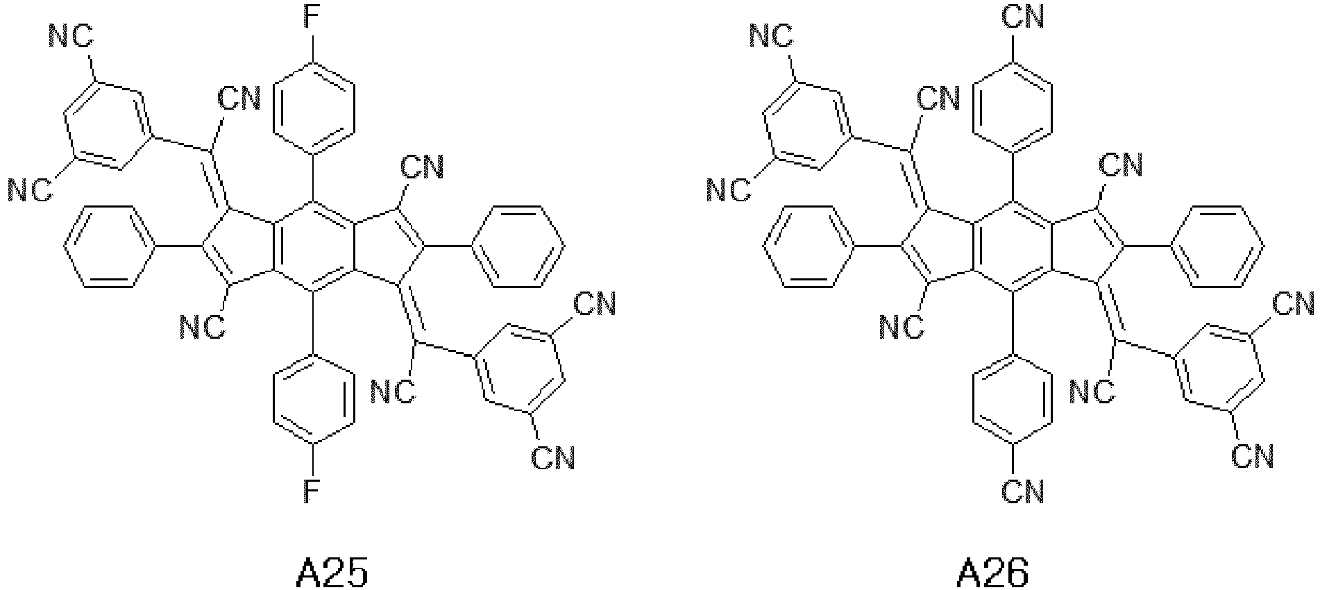


- The organic light emitting display device of any one of claims 1 to 3, wherein the compound represented by the above Chemical Formula 2 is one among the following compounds:


- The organic light emitting display device of any one of claims 1 to 4, wherein the at least one organic layer includes a hole injection layer.
- The organic light emitting display device of claim 5, wherein a dopant of the hole injection layer includes the compound.
- The organic light emitting display device of claim 5, wherein the hole injection layer includes the compound.
- The organic light emitting display device of any one of claims 1 to 7, wherein the at least one organic layer includes a P-type charge generation layer.
- The organic light emitting display device of claim 8, wherein a dopant of the P-type charge generation layer includes the compound.
- The organic light emitting display device of claim 8, wherein the P-type charge generation layer includes the compound.
- The organic light emitting display device of any one of claims 1 to 10, comprising:at least one light emitting part between an anode and a cathode, and the at least one light emitting part having a hole injection layer and a light emitting layer; anda charge generation layer having a P-type charge generation layer between the at least one light emitting parts,wherein at least one among the hole injection layer and the P-type charge generation layer comprises the compound represented by Chemical Formula 1 or 2.
Priority Applications (2)
| Application Number | Priority Date | Filing Date | Title |
|---|---|---|---|
| EP22153431.6A EP4009392A1 (en) | 2015-12-03 | 2016-08-04 | Organic light emitting display device |
| EP20194870.0A EP3767696B1 (en) | 2015-12-03 | 2016-08-04 | Organic light emitting display device |
Applications Claiming Priority (2)
| Application Number | Priority Date | Filing Date | Title |
|---|---|---|---|
| KR20150171452 | 2015-12-03 | ||
| KR1020160057107A KR102279375B1 (en) | 2015-12-03 | 2016-05-10 | Organic Light Emitting Diode Device |
Related Child Applications (3)
| Application Number | Title | Priority Date | Filing Date |
|---|---|---|---|
| EP22153431.6A Division EP4009392A1 (en) | 2015-12-03 | 2016-08-04 | Organic light emitting display device |
| EP20194870.0A Division EP3767696B1 (en) | 2015-12-03 | 2016-08-04 | Organic light emitting display device |
| EP20194870.0A Division-Into EP3767696B1 (en) | 2015-12-03 | 2016-08-04 | Organic light emitting display device |
Publications (2)
| Publication Number | Publication Date |
|---|---|
| EP3176844A1 true EP3176844A1 (en) | 2017-06-07 |
| EP3176844B1 EP3176844B1 (en) | 2020-11-18 |
Family
ID=56799237
Family Applications (1)
| Application Number | Title | Priority Date | Filing Date |
|---|---|---|---|
| EP16182682.1A Active EP3176844B1 (en) | 2015-12-03 | 2016-08-04 | Organic light emitting display device |
Country Status (2)
| Country | Link |
|---|---|
| US (2) | US10658593B2 (en) |
| EP (1) | EP3176844B1 (en) |
Cited By (9)
| Publication number | Priority date | Publication date | Assignee | Title |
|---|---|---|---|---|
| EP3846240A1 (en) * | 2019-12-31 | 2021-07-07 | LG Display Co., Ltd. | Organic electric element, display panel comprising the same and display device comprising the same |
| EP3846238A1 (en) * | 2019-12-31 | 2021-07-07 | LG Display Co., Ltd. | Organic electric element, display panel comprising the same and display device comprising the same |
| EP3846233A1 (en) * | 2019-12-31 | 2021-07-07 | LG Display Co., Ltd. | Organic electric element, display panel comprising the same and display device comprising the same |
| EP3846242A1 (en) * | 2019-12-31 | 2021-07-07 | LG Display Co., Ltd. | Organic electric element, display panel comprising the same and display device comprising the same |
| EP3846241A1 (en) * | 2019-12-31 | 2021-07-07 | LG Display Co., Ltd. | Organic electric element, display panel comprising the same and display device comprising the same |
| EP3846237A1 (en) * | 2019-12-31 | 2021-07-07 | LG Display Co., Ltd. | Organic electric element, display panel comprising the same and display device comprising the same |
| EP3846239A1 (en) * | 2019-12-31 | 2021-07-07 | LG Display Co., Ltd. | Organic electric element, display panel comprising the same and display device comprising the same |
| EP4216697A1 (en) * | 2019-12-31 | 2023-07-26 | LG Display Co., Ltd. | Organic electric element, display panel comprising the same and display device comprising the same |
| CN113130815B (en) * | 2019-12-31 | 2024-05-03 | 乐金显示有限公司 | Organic electronic element, display panel including the same, and display device including the same |
Families Citing this family (4)
| Publication number | Priority date | Publication date | Assignee | Title |
|---|---|---|---|---|
| KR102498847B1 (en) * | 2014-12-03 | 2023-02-13 | 삼성디스플레이 주식회사 | Organic electroluminescence device |
| KR102348376B1 (en) * | 2015-09-30 | 2022-01-06 | 엘지디스플레이 주식회사 | Organic light emitting device |
| CN107464833B (en) | 2017-09-28 | 2020-06-09 | 京东方科技集团股份有限公司 | Laminated OLED display panel, manufacturing method thereof and display device |
| CN114843410A (en) * | 2021-01-30 | 2022-08-02 | 北京夏禾科技有限公司 | Laminated organic electroluminescent device |
Citations (3)
| Publication number | Priority date | Publication date | Assignee | Title |
|---|---|---|---|---|
| WO2008106210A1 (en) * | 2007-02-28 | 2008-09-04 | E. I. Du Pont De Nemours And Company | Organic electronic device |
| WO2013190427A1 (en) * | 2012-06-19 | 2013-12-27 | Koninklijke Philips N.V. | Organic electroluminescent device |
| US20140183493A1 (en) * | 2012-12-28 | 2014-07-03 | Lg Display Co., Ltd. | Organic Light Emitting Display Device and Method of Fabricating the Same |
Family Cites Families (7)
| Publication number | Priority date | Publication date | Assignee | Title |
|---|---|---|---|---|
| EP2185496A1 (en) * | 2007-08-02 | 2010-05-19 | Northwestern University | Conjugated monomers and polymers and preparation and use thereof |
| KR101434359B1 (en) | 2007-10-08 | 2014-08-26 | 삼성디스플레이 주식회사 | White Organic light emitting device |
| WO2013051234A1 (en) | 2011-10-04 | 2013-04-11 | ソニー株式会社 | Organic electroluminescent element |
| GB2508289B (en) * | 2012-10-31 | 2015-09-30 | Lg Display Co Ltd | Organic light emitting display device |
| DE102013112602B4 (en) * | 2012-12-18 | 2020-11-12 | Lg Display Co., Ltd. | White organic light emitting device |
| KR102279375B1 (en) | 2015-12-03 | 2021-07-22 | 엘지디스플레이 주식회사 | Organic Light Emitting Diode Device |
| KR102486441B1 (en) | 2017-12-28 | 2023-01-06 | 엘지디스플레이 주식회사 | Organic light emitting diode |
-
2016
- 2016-08-04 EP EP16182682.1A patent/EP3176844B1/en active Active
- 2016-08-29 US US15/250,214 patent/US10658593B2/en active Active
-
2020
- 2020-04-07 US US16/842,486 patent/US11158808B2/en active Active
Patent Citations (3)
| Publication number | Priority date | Publication date | Assignee | Title |
|---|---|---|---|---|
| WO2008106210A1 (en) * | 2007-02-28 | 2008-09-04 | E. I. Du Pont De Nemours And Company | Organic electronic device |
| WO2013190427A1 (en) * | 2012-06-19 | 2013-12-27 | Koninklijke Philips N.V. | Organic electroluminescent device |
| US20140183493A1 (en) * | 2012-12-28 | 2014-07-03 | Lg Display Co., Ltd. | Organic Light Emitting Display Device and Method of Fabricating the Same |
Non-Patent Citations (3)
| Title |
|---|
| H.Z. CHEN ET AL: "Synthesis, optical and electroluminescent properties of a novel Indacene", SYNTHETIC METALS, vol. 139, no. 2, 5 September 2003 (2003-09-05), CH, pages 529 - 534, XP055326460, ISSN: 0379-6779, DOI: 10.1016/S0379-6779(03)00338-2 * |
| XIAOZHANG ZHU ET AL: "Modular Synthesis of 1 H -Indenes, Dihydro- s -Indacene, and Diindenoindacene-a Carbon-Bridged p -Phenylenevinylene Congener", JOURNAL OF THE AMERICAN CHEMICAL SOCIETY, vol. 131, no. 38, 30 September 2009 (2009-09-30), pages 13596 - 13597, XP055366099, ISSN: 0002-7863, DOI: 10.1021/ja905626b * |
| YASUTAKA ENDO ET AL: "Synthesis and Electronic Structure of Dicyanofulvene-Fused Electron Accepting Molecule Based on a 1,5-Dihydro- s -Indacene Framework", ORGANIC LETTERS , 14(23), 6012-6015 CODEN: ORLEF7; ISSN: 1523-7052, vol. 16, no. 21, 7 November 2014 (2014-11-07), pages 5608 - 5611, XP055365865, ISSN: 1523-7060, DOI: 10.1021/ol502675n * |
Cited By (17)
| Publication number | Priority date | Publication date | Assignee | Title |
|---|---|---|---|---|
| EP3846240A1 (en) * | 2019-12-31 | 2021-07-07 | LG Display Co., Ltd. | Organic electric element, display panel comprising the same and display device comprising the same |
| EP3846238A1 (en) * | 2019-12-31 | 2021-07-07 | LG Display Co., Ltd. | Organic electric element, display panel comprising the same and display device comprising the same |
| EP3846233A1 (en) * | 2019-12-31 | 2021-07-07 | LG Display Co., Ltd. | Organic electric element, display panel comprising the same and display device comprising the same |
| EP3846242A1 (en) * | 2019-12-31 | 2021-07-07 | LG Display Co., Ltd. | Organic electric element, display panel comprising the same and display device comprising the same |
| EP3846241A1 (en) * | 2019-12-31 | 2021-07-07 | LG Display Co., Ltd. | Organic electric element, display panel comprising the same and display device comprising the same |
| EP3846237A1 (en) * | 2019-12-31 | 2021-07-07 | LG Display Co., Ltd. | Organic electric element, display panel comprising the same and display device comprising the same |
| EP3846239A1 (en) * | 2019-12-31 | 2021-07-07 | LG Display Co., Ltd. | Organic electric element, display panel comprising the same and display device comprising the same |
| CN113130830A (en) * | 2019-12-31 | 2021-07-16 | 乐金显示有限公司 | Organic electronic element, display panel including the same, and display device including the same |
| CN113130815A (en) * | 2019-12-31 | 2021-07-16 | 乐金显示有限公司 | Organic electronic element, display panel including the same, and display device including the same |
| CN113130828A (en) * | 2019-12-31 | 2021-07-16 | 乐金显示有限公司 | Organic electronic element, display panel including the same, and display device including the same |
| CN113130831A (en) * | 2019-12-31 | 2021-07-16 | 乐金显示有限公司 | Organic electronic element, display panel including the same, and display device including the same |
| US11430964B2 (en) | 2019-12-31 | 2022-08-30 | Lg Display Co., Ltd. | Organic electric element, display panel comprising the same and display device comprising the same |
| EP4216697A1 (en) * | 2019-12-31 | 2023-07-26 | LG Display Co., Ltd. | Organic electric element, display panel comprising the same and display device comprising the same |
| CN113130828B (en) * | 2019-12-31 | 2024-01-19 | 乐金显示有限公司 | Organic electronic element, display panel including the same, and display device including the same |
| CN113130830B (en) * | 2019-12-31 | 2024-02-06 | 乐金显示有限公司 | Organic electronic element, display panel including the same, and display device including the same |
| CN113130831B (en) * | 2019-12-31 | 2024-03-29 | 乐金显示有限公司 | Organic electronic element, display panel including the same, and display device including the same |
| CN113130815B (en) * | 2019-12-31 | 2024-05-03 | 乐金显示有限公司 | Organic electronic element, display panel including the same, and display device including the same |
Also Published As
| Publication number | Publication date |
|---|---|
| US20200235302A1 (en) | 2020-07-23 |
| US10658593B2 (en) | 2020-05-19 |
| US20170162792A1 (en) | 2017-06-08 |
| US11158808B2 (en) | 2021-10-26 |
| EP3176844B1 (en) | 2020-11-18 |
Similar Documents
| Publication | Publication Date | Title |
|---|---|---|
| EP3176844B1 (en) | Organic light emitting display device | |
| US11600784B2 (en) | Organic light emitting display device | |
| EP3107131B1 (en) | Organic light emitting display device | |
| US11349079B2 (en) | Organic light emitting display device | |
| EP3133655B1 (en) | Organic light emitting display device | |
| EP3174123B1 (en) | Organic light emitting display device | |
| US10355220B2 (en) | Organic light emitting display device | |
| CN111081888B (en) | Organic light emitting diode and organic light emitting device having the same | |
| KR102152013B1 (en) | Organic light emitting diode device comprising organic compounds | |
| KR102145425B1 (en) | Organic compounds and organic light emitting diode device comprising the same |
Legal Events
| Date | Code | Title | Description |
|---|---|---|---|
| 17P | Request for examination filed |
Effective date: 20160804 |
|
| AK | Designated contracting states |
Kind code of ref document: A1 Designated state(s): AL AT BE BG CH CY CZ DE DK EE ES FI FR GB GR HR HU IE IS IT LI LT LU LV MC MK MT NL NO PL PT RO RS SE SI SK SM TR |
|
| AX | Request for extension of the european patent |
Extension state: BA ME |
|
| PUAI | Public reference made under article 153(3) epc to a published international application that has entered the european phase |
Free format text: ORIGINAL CODE: 0009012 |
|
| STAA | Information on the status of an ep patent application or granted ep patent |
Free format text: STATUS: REQUEST FOR EXAMINATION WAS MADE |
|
| RBV | Designated contracting states (corrected) |
Designated state(s): AL AT BE BG CH CY CZ DE DK EE ES FI FR GB GR HR HU IE IS IT LI LT LU LV MC MK MT NL NO PL PT RO RS SE SI SK SM TR |
|
| REG | Reference to a national code |
Ref country code: DE Ref legal event code: R079 Ref document number: 602016047969 Country of ref document: DE Free format text: PREVIOUS MAIN CLASS: H01L0051000000 Ipc: H01L0051540000 |
|
| RIC1 | Information provided on ipc code assigned before grant |
Ipc: H01L 51/54 20060101AFI20200305BHEP |
|
| GRAP | Despatch of communication of intention to grant a patent |
Free format text: ORIGINAL CODE: EPIDOSNIGR1 |
|
| STAA | Information on the status of an ep patent application or granted ep patent |
Free format text: STATUS: GRANT OF PATENT IS INTENDED |
|
| INTG | Intention to grant announced |
Effective date: 20200612 |
|
| GRAS | Grant fee paid |
Free format text: ORIGINAL CODE: EPIDOSNIGR3 |
|
| GRAA | (expected) grant |
Free format text: ORIGINAL CODE: 0009210 |
|
| STAA | Information on the status of an ep patent application or granted ep patent |
Free format text: STATUS: THE PATENT HAS BEEN GRANTED |
|
| AK | Designated contracting states |
Kind code of ref document: B1 Designated state(s): AL AT BE BG CH CY CZ DE DK EE ES FI FR GB GR HR HU IE IS IT LI LT LU LV MC MK MT NL NO PL PT RO RS SE SI SK SM TR |
|
| REG | Reference to a national code |
Ref country code: GB Ref legal event code: FG4D |
|
| REG | Reference to a national code |
Ref country code: CH Ref legal event code: NV Representative=s name: RENTSCH PARTNER AG, CH Ref country code: CH Ref legal event code: EP |
|
| REG | Reference to a national code |
Ref country code: DE Ref legal event code: R096 Ref document number: 602016047969 Country of ref document: DE |
|
| REG | Reference to a national code |
Ref country code: IE Ref legal event code: FG4D |
|
| REG | Reference to a national code |
Ref country code: AT Ref legal event code: REF Ref document number: 1336745 Country of ref document: AT Kind code of ref document: T Effective date: 20201215 |
|
| REG | Reference to a national code |
Ref country code: AT Ref legal event code: MK05 Ref document number: 1336745 Country of ref document: AT Kind code of ref document: T Effective date: 20201118 |
|
| REG | Reference to a national code |
Ref country code: NL Ref legal event code: MP Effective date: 20201118 |
|
| PG25 | Lapsed in a contracting state [announced via postgrant information from national office to epo] |
Ref country code: FI Free format text: LAPSE BECAUSE OF FAILURE TO SUBMIT A TRANSLATION OF THE DESCRIPTION OR TO PAY THE FEE WITHIN THE PRESCRIBED TIME-LIMIT Effective date: 20201118 Ref country code: GR Free format text: LAPSE BECAUSE OF FAILURE TO SUBMIT A TRANSLATION OF THE DESCRIPTION OR TO PAY THE FEE WITHIN THE PRESCRIBED TIME-LIMIT Effective date: 20210219 Ref country code: RS Free format text: LAPSE BECAUSE OF FAILURE TO SUBMIT A TRANSLATION OF THE DESCRIPTION OR TO PAY THE FEE WITHIN THE PRESCRIBED TIME-LIMIT Effective date: 20201118 Ref country code: PT Free format text: LAPSE BECAUSE OF FAILURE TO SUBMIT A TRANSLATION OF THE DESCRIPTION OR TO PAY THE FEE WITHIN THE PRESCRIBED TIME-LIMIT Effective date: 20210318 Ref country code: NO Free format text: LAPSE BECAUSE OF FAILURE TO SUBMIT A TRANSLATION OF THE DESCRIPTION OR TO PAY THE FEE WITHIN THE PRESCRIBED TIME-LIMIT Effective date: 20210218 |
|
| PG25 | Lapsed in a contracting state [announced via postgrant information from national office to epo] |
Ref country code: BG Free format text: LAPSE BECAUSE OF FAILURE TO SUBMIT A TRANSLATION OF THE DESCRIPTION OR TO PAY THE FEE WITHIN THE PRESCRIBED TIME-LIMIT Effective date: 20210218 Ref country code: LV Free format text: LAPSE BECAUSE OF FAILURE TO SUBMIT A TRANSLATION OF THE DESCRIPTION OR TO PAY THE FEE WITHIN THE PRESCRIBED TIME-LIMIT Effective date: 20201118 Ref country code: IS Free format text: LAPSE BECAUSE OF FAILURE TO SUBMIT A TRANSLATION OF THE DESCRIPTION OR TO PAY THE FEE WITHIN THE PRESCRIBED TIME-LIMIT Effective date: 20210318 Ref country code: SE Free format text: LAPSE BECAUSE OF FAILURE TO SUBMIT A TRANSLATION OF THE DESCRIPTION OR TO PAY THE FEE WITHIN THE PRESCRIBED TIME-LIMIT Effective date: 20201118 Ref country code: PL Free format text: LAPSE BECAUSE OF FAILURE TO SUBMIT A TRANSLATION OF THE DESCRIPTION OR TO PAY THE FEE WITHIN THE PRESCRIBED TIME-LIMIT Effective date: 20201118 Ref country code: AT Free format text: LAPSE BECAUSE OF FAILURE TO SUBMIT A TRANSLATION OF THE DESCRIPTION OR TO PAY THE FEE WITHIN THE PRESCRIBED TIME-LIMIT Effective date: 20201118 |
|
| REG | Reference to a national code |
Ref country code: LT Ref legal event code: MG9D |
|
| PG25 | Lapsed in a contracting state [announced via postgrant information from national office to epo] |
Ref country code: HR Free format text: LAPSE BECAUSE OF FAILURE TO SUBMIT A TRANSLATION OF THE DESCRIPTION OR TO PAY THE FEE WITHIN THE PRESCRIBED TIME-LIMIT Effective date: 20201118 |
|
| PG25 | Lapsed in a contracting state [announced via postgrant information from national office to epo] |
Ref country code: RO Free format text: LAPSE BECAUSE OF FAILURE TO SUBMIT A TRANSLATION OF THE DESCRIPTION OR TO PAY THE FEE WITHIN THE PRESCRIBED TIME-LIMIT Effective date: 20201118 Ref country code: SK Free format text: LAPSE BECAUSE OF FAILURE TO SUBMIT A TRANSLATION OF THE DESCRIPTION OR TO PAY THE FEE WITHIN THE PRESCRIBED TIME-LIMIT Effective date: 20201118 Ref country code: EE Free format text: LAPSE BECAUSE OF FAILURE TO SUBMIT A TRANSLATION OF THE DESCRIPTION OR TO PAY THE FEE WITHIN THE PRESCRIBED TIME-LIMIT Effective date: 20201118 Ref country code: CZ Free format text: LAPSE BECAUSE OF FAILURE TO SUBMIT A TRANSLATION OF THE DESCRIPTION OR TO PAY THE FEE WITHIN THE PRESCRIBED TIME-LIMIT Effective date: 20201118 Ref country code: SM Free format text: LAPSE BECAUSE OF FAILURE TO SUBMIT A TRANSLATION OF THE DESCRIPTION OR TO PAY THE FEE WITHIN THE PRESCRIBED TIME-LIMIT Effective date: 20201118 Ref country code: LT Free format text: LAPSE BECAUSE OF FAILURE TO SUBMIT A TRANSLATION OF THE DESCRIPTION OR TO PAY THE FEE WITHIN THE PRESCRIBED TIME-LIMIT Effective date: 20201118 |
|
| REG | Reference to a national code |
Ref country code: DE Ref legal event code: R097 Ref document number: 602016047969 Country of ref document: DE |
|
| PG25 | Lapsed in a contracting state [announced via postgrant information from national office to epo] |
Ref country code: DK Free format text: LAPSE BECAUSE OF FAILURE TO SUBMIT A TRANSLATION OF THE DESCRIPTION OR TO PAY THE FEE WITHIN THE PRESCRIBED TIME-LIMIT Effective date: 20201118 |
|
| PLBE | No opposition filed within time limit |
Free format text: ORIGINAL CODE: 0009261 |
|
| STAA | Information on the status of an ep patent application or granted ep patent |
Free format text: STATUS: NO OPPOSITION FILED WITHIN TIME LIMIT |
|
| 26N | No opposition filed |
Effective date: 20210819 |
|
| PG25 | Lapsed in a contracting state [announced via postgrant information from national office to epo] |
Ref country code: NL Free format text: LAPSE BECAUSE OF FAILURE TO SUBMIT A TRANSLATION OF THE DESCRIPTION OR TO PAY THE FEE WITHIN THE PRESCRIBED TIME-LIMIT Effective date: 20201118 Ref country code: AL Free format text: LAPSE BECAUSE OF FAILURE TO SUBMIT A TRANSLATION OF THE DESCRIPTION OR TO PAY THE FEE WITHIN THE PRESCRIBED TIME-LIMIT Effective date: 20201118 Ref country code: IT Free format text: LAPSE BECAUSE OF FAILURE TO SUBMIT A TRANSLATION OF THE DESCRIPTION OR TO PAY THE FEE WITHIN THE PRESCRIBED TIME-LIMIT Effective date: 20201118 |
|
| PG25 | Lapsed in a contracting state [announced via postgrant information from national office to epo] |
Ref country code: SI Free format text: LAPSE BECAUSE OF FAILURE TO SUBMIT A TRANSLATION OF THE DESCRIPTION OR TO PAY THE FEE WITHIN THE PRESCRIBED TIME-LIMIT Effective date: 20201118 |
|
| PG25 | Lapsed in a contracting state [announced via postgrant information from national office to epo] |
Ref country code: ES Free format text: LAPSE BECAUSE OF FAILURE TO SUBMIT A TRANSLATION OF THE DESCRIPTION OR TO PAY THE FEE WITHIN THE PRESCRIBED TIME-LIMIT Effective date: 20201118 |
|
| PG25 | Lapsed in a contracting state [announced via postgrant information from national office to epo] |
Ref country code: MC Free format text: LAPSE BECAUSE OF FAILURE TO SUBMIT A TRANSLATION OF THE DESCRIPTION OR TO PAY THE FEE WITHIN THE PRESCRIBED TIME-LIMIT Effective date: 20201118 |
|
| REG | Reference to a national code |
Ref country code: BE Ref legal event code: MM Effective date: 20210831 |
|
| PG25 | Lapsed in a contracting state [announced via postgrant information from national office to epo] |
Ref country code: IS Free format text: LAPSE BECAUSE OF FAILURE TO SUBMIT A TRANSLATION OF THE DESCRIPTION OR TO PAY THE FEE WITHIN THE PRESCRIBED TIME-LIMIT Effective date: 20210318 Ref country code: LU Free format text: LAPSE BECAUSE OF NON-PAYMENT OF DUE FEES Effective date: 20210804 |
|
| PG25 | Lapsed in a contracting state [announced via postgrant information from national office to epo] |
Ref country code: IE Free format text: LAPSE BECAUSE OF NON-PAYMENT OF DUE FEES Effective date: 20210804 Ref country code: BE Free format text: LAPSE BECAUSE OF NON-PAYMENT OF DUE FEES Effective date: 20210831 |
|
| REG | Reference to a national code |
Ref country code: DE Ref legal event code: R079 Ref document number: 602016047969 Country of ref document: DE Free format text: PREVIOUS MAIN CLASS: H01L0051540000 Ipc: H10K0085000000 |
|
| PG25 | Lapsed in a contracting state [announced via postgrant information from national office to epo] |
Ref country code: HU Free format text: LAPSE BECAUSE OF FAILURE TO SUBMIT A TRANSLATION OF THE DESCRIPTION OR TO PAY THE FEE WITHIN THE PRESCRIBED TIME-LIMIT; INVALID AB INITIO Effective date: 20160804 |
|
| PG25 | Lapsed in a contracting state [announced via postgrant information from national office to epo] |
Ref country code: CY Free format text: LAPSE BECAUSE OF FAILURE TO SUBMIT A TRANSLATION OF THE DESCRIPTION OR TO PAY THE FEE WITHIN THE PRESCRIBED TIME-LIMIT Effective date: 20201118 |
|
| PGFP | Annual fee paid to national office [announced via postgrant information from national office to epo] |
Ref country code: FR Payment date: 20230621 Year of fee payment: 8 |
|
| PGFP | Annual fee paid to national office [announced via postgrant information from national office to epo] |
Ref country code: GB Payment date: 20230620 Year of fee payment: 8 Ref country code: CH Payment date: 20230901 Year of fee payment: 8 |
|
| PGFP | Annual fee paid to national office [announced via postgrant information from national office to epo] |
Ref country code: DE Payment date: 20230620 Year of fee payment: 8 |
|
| REG | Reference to a national code |
Ref country code: DE Ref legal event code: R082 Ref document number: 602016047969 Country of ref document: DE Representative=s name: TER MEER STEINMEISTER & PARTNER PATENTANWAELTE, DE |