EP3846233A1 - Organic electric element, display panel comprising the same and display device comprising the same - Google Patents
Organic electric element, display panel comprising the same and display device comprising the same Download PDFInfo
- Publication number
- EP3846233A1 EP3846233A1 EP20212711.4A EP20212711A EP3846233A1 EP 3846233 A1 EP3846233 A1 EP 3846233A1 EP 20212711 A EP20212711 A EP 20212711A EP 3846233 A1 EP3846233 A1 EP 3846233A1
- Authority
- EP
- European Patent Office
- Prior art keywords
- compound
- layer
- electric element
- organic electric
- organic
- Prior art date
- Legal status (The legal status is an assumption and is not a legal conclusion. Google has not performed a legal analysis and makes no representation as to the accuracy of the status listed.)
- Granted
Links
Images


Classifications
-
- H—ELECTRICITY
- H10—SEMICONDUCTOR DEVICES; ELECTRIC SOLID-STATE DEVICES NOT OTHERWISE PROVIDED FOR
- H10K—ORGANIC ELECTRIC SOLID-STATE DEVICES
- H10K85/00—Organic materials used in the body or electrodes of devices covered by this subclass
- H10K85/60—Organic compounds having low molecular weight
- H10K85/615—Polycyclic condensed aromatic hydrocarbons, e.g. anthracene
-
- H—ELECTRICITY
- H10—SEMICONDUCTOR DEVICES; ELECTRIC SOLID-STATE DEVICES NOT OTHERWISE PROVIDED FOR
- H10K—ORGANIC ELECTRIC SOLID-STATE DEVICES
- H10K50/00—Organic light-emitting devices
- H10K50/10—OLEDs or polymer light-emitting diodes [PLED]
- H10K50/14—Carrier transporting layers
- H10K50/15—Hole transporting layers
-
- H—ELECTRICITY
- H10—SEMICONDUCTOR DEVICES; ELECTRIC SOLID-STATE DEVICES NOT OTHERWISE PROVIDED FOR
- H10K—ORGANIC ELECTRIC SOLID-STATE DEVICES
- H10K50/00—Organic light-emitting devices
- H10K50/10—OLEDs or polymer light-emitting diodes [PLED]
- H10K50/14—Carrier transporting layers
- H10K50/15—Hole transporting layers
- H10K50/155—Hole transporting layers comprising dopants
-
- H—ELECTRICITY
- H10—SEMICONDUCTOR DEVICES; ELECTRIC SOLID-STATE DEVICES NOT OTHERWISE PROVIDED FOR
- H10K—ORGANIC ELECTRIC SOLID-STATE DEVICES
- H10K50/00—Organic light-emitting devices
- H10K50/10—OLEDs or polymer light-emitting diodes [PLED]
- H10K50/11—OLEDs or polymer light-emitting diodes [PLED] characterised by the electroluminescent [EL] layers
-
- H—ELECTRICITY
- H10—SEMICONDUCTOR DEVICES; ELECTRIC SOLID-STATE DEVICES NOT OTHERWISE PROVIDED FOR
- H10K—ORGANIC ELECTRIC SOLID-STATE DEVICES
- H10K50/00—Organic light-emitting devices
- H10K50/10—OLEDs or polymer light-emitting diodes [PLED]
- H10K50/14—Carrier transporting layers
- H10K50/15—Hole transporting layers
- H10K50/156—Hole transporting layers comprising a multilayered structure
-
- H—ELECTRICITY
- H10—SEMICONDUCTOR DEVICES; ELECTRIC SOLID-STATE DEVICES NOT OTHERWISE PROVIDED FOR
- H10K—ORGANIC ELECTRIC SOLID-STATE DEVICES
- H10K50/00—Organic light-emitting devices
- H10K50/10—OLEDs or polymer light-emitting diodes [PLED]
- H10K50/19—Tandem OLEDs
-
- H—ELECTRICITY
- H10—SEMICONDUCTOR DEVICES; ELECTRIC SOLID-STATE DEVICES NOT OTHERWISE PROVIDED FOR
- H10K—ORGANIC ELECTRIC SOLID-STATE DEVICES
- H10K59/00—Integrated devices, or assemblies of multiple devices, comprising at least one organic light-emitting element covered by group H10K50/00
- H10K59/10—OLED displays
- H10K59/12—Active-matrix OLED [AMOLED] displays
-
- H—ELECTRICITY
- H10—SEMICONDUCTOR DEVICES; ELECTRIC SOLID-STATE DEVICES NOT OTHERWISE PROVIDED FOR
- H10K—ORGANIC ELECTRIC SOLID-STATE DEVICES
- H10K85/00—Organic materials used in the body or electrodes of devices covered by this subclass
-
- H—ELECTRICITY
- H10—SEMICONDUCTOR DEVICES; ELECTRIC SOLID-STATE DEVICES NOT OTHERWISE PROVIDED FOR
- H10K—ORGANIC ELECTRIC SOLID-STATE DEVICES
- H10K85/00—Organic materials used in the body or electrodes of devices covered by this subclass
- H10K85/30—Coordination compounds
- H10K85/341—Transition metal complexes, e.g. Ru(II)polypyridine complexes
- H10K85/342—Transition metal complexes, e.g. Ru(II)polypyridine complexes comprising iridium
-
- H—ELECTRICITY
- H10—SEMICONDUCTOR DEVICES; ELECTRIC SOLID-STATE DEVICES NOT OTHERWISE PROVIDED FOR
- H10K—ORGANIC ELECTRIC SOLID-STATE DEVICES
- H10K85/00—Organic materials used in the body or electrodes of devices covered by this subclass
- H10K85/60—Organic compounds having low molecular weight
- H10K85/615—Polycyclic condensed aromatic hydrocarbons, e.g. anthracene
- H10K85/626—Polycyclic condensed aromatic hydrocarbons, e.g. anthracene containing more than one polycyclic condensed aromatic rings, e.g. bis-anthracene
-
- H—ELECTRICITY
- H10—SEMICONDUCTOR DEVICES; ELECTRIC SOLID-STATE DEVICES NOT OTHERWISE PROVIDED FOR
- H10K—ORGANIC ELECTRIC SOLID-STATE DEVICES
- H10K85/00—Organic materials used in the body or electrodes of devices covered by this subclass
- H10K85/60—Organic compounds having low molecular weight
- H10K85/631—Amine compounds having at least two aryl rest on at least one amine-nitrogen atom, e.g. triphenylamine
-
- H—ELECTRICITY
- H10—SEMICONDUCTOR DEVICES; ELECTRIC SOLID-STATE DEVICES NOT OTHERWISE PROVIDED FOR
- H10K—ORGANIC ELECTRIC SOLID-STATE DEVICES
- H10K85/00—Organic materials used in the body or electrodes of devices covered by this subclass
- H10K85/60—Organic compounds having low molecular weight
- H10K85/631—Amine compounds having at least two aryl rest on at least one amine-nitrogen atom, e.g. triphenylamine
- H10K85/633—Amine compounds having at least two aryl rest on at least one amine-nitrogen atom, e.g. triphenylamine comprising polycyclic condensed aromatic hydrocarbons as substituents on the nitrogen atom
-
- H—ELECTRICITY
- H10—SEMICONDUCTOR DEVICES; ELECTRIC SOLID-STATE DEVICES NOT OTHERWISE PROVIDED FOR
- H10K—ORGANIC ELECTRIC SOLID-STATE DEVICES
- H10K85/00—Organic materials used in the body or electrodes of devices covered by this subclass
- H10K85/60—Organic compounds having low molecular weight
- H10K85/649—Aromatic compounds comprising a hetero atom
- H10K85/654—Aromatic compounds comprising a hetero atom comprising only nitrogen as heteroatom
-
- H—ELECTRICITY
- H10—SEMICONDUCTOR DEVICES; ELECTRIC SOLID-STATE DEVICES NOT OTHERWISE PROVIDED FOR
- H10K—ORGANIC ELECTRIC SOLID-STATE DEVICES
- H10K85/00—Organic materials used in the body or electrodes of devices covered by this subclass
- H10K85/60—Organic compounds having low molecular weight
- H10K85/649—Aromatic compounds comprising a hetero atom
- H10K85/657—Polycyclic condensed heteroaromatic hydrocarbons
- H10K85/6572—Polycyclic condensed heteroaromatic hydrocarbons comprising only nitrogen in the heteroaromatic polycondensed ring system, e.g. phenanthroline or carbazole
-
- H—ELECTRICITY
- H10—SEMICONDUCTOR DEVICES; ELECTRIC SOLID-STATE DEVICES NOT OTHERWISE PROVIDED FOR
- H10K—ORGANIC ELECTRIC SOLID-STATE DEVICES
- H10K2101/00—Properties of the organic materials covered by group H10K85/00
- H10K2101/30—Highest occupied molecular orbital [HOMO], lowest unoccupied molecular orbital [LUMO] or Fermi energy values
-
- H—ELECTRICITY
- H10—SEMICONDUCTOR DEVICES; ELECTRIC SOLID-STATE DEVICES NOT OTHERWISE PROVIDED FOR
- H10K—ORGANIC ELECTRIC SOLID-STATE DEVICES
- H10K2101/00—Properties of the organic materials covered by group H10K85/00
- H10K2101/40—Interrelation of parameters between multiple constituent active layers or sublayers, e.g. HOMO values in adjacent layers
Definitions
- Embodiments of the present disclosure relate to an organic electric element, a display panel and a display device including the organic electric element.
- an organic light emitting phenomenon refers to the phenomenon of converting electrical energy into light energy by using an organic material.
- An organic electric element refers to an electric element using the organic light emitting phenomenon.
- An organic electric element using the organic light emitting phenomenon can be applied to a display device. Since a portable display device is driven by a battery, which is a limited power source, an organic electric element used in the portable display device requires excellent light emission efficiency. In addition, since an image should be displayed normally during the use of an electronic device, a long life of the organic electric element can be also needed.
- Embodiments of the present disclosure can provide an organic electric element having high efficiency and/or long life.
- Embodiments of the present disclosure can provide a display panel having high efficiency and/or long life by including the above-described organic electric element.
- embodiments of the present disclosure can provide a display device having high efficiency and/or long life by including the above-described display panel.
- embodiments of the present disclosure provide an organic electric element according to claim 1. Further embodiments are described in the dependent claims. According to an aspect, embodiments of the present disclosure can provide an organic electric element comprising a first electrode, a second electrode and an organic layer.
- the organic layer is positioned between the first electrode and the second electrode.
- the organic layer comprises a light emitting layer and a first layer.
- the first layer comprises a first compound, a second compound and a third compound.
- the first compound has a HOMO (Highest Occupied Molecular Orbital) energy level of -5.5 eV to -5.0 eV.
- HOMO Highest Occupied Molecular Orbital
- the organic electric element satisfies the following general formula 1. 0.1 eV ⁇ L 3 ⁇ L 2 ⁇ 0.5 eV
- L 3 is a LUMO (Lowest Unoccupied Molecular Orbital) energy level of the third compound
- L 2 is a LUMO (Lowest Unoccupied Molecular Orbital) energy level of the second compound.
- the second compound and the third compound have the LUMO energy level of -4.0 eV or less, respectively.
- the LUMO energy level of the third compound is greater than the HOMO energy level of the first compound.
- the first compound and the third compound included in the organic electric element satisfy the following general formula 2. 2.0 eV ⁇ L 1 ⁇ L 3 ⁇ 3.0 eV
- L 1 is the LUMO energy level of the first compound.
- the first compound and the third compound included in the organic electric element satisfy the following general formula 3. 0.2 eV ⁇ L 3 ⁇ H 1 ⁇ 1.0 eV
- H 1 is the HOMO energy level of the first compound.
- the first layer is positioned between the first electrode and the light emitting layer.
- the organic layer comprises two or more light emitting layers, and the first layer is positioned between the first electrode and one of the two or more light emitting layers.
- the organic layer comprises two or more light emitting layers, and the first layer is positioned between the light emitting layers.
- the first compound includes a tertiary amine-based material.
- the second compound is a cyanocarbon-based material.
- the third compound includes an indacene-based material.
- a sum of a weight of the second compound and a weight of the third compound is approximately 0.1% to 50% by weight according to a total weight of the first compound, the second compound, and the third compound.
- a ratio (A:B) of a weight (A) of the second compound and a weight (B) of the third compound included in the first layer is approximately (1:99) to (99:1).
- Embodiments of the present disclosure can provide a display panel comprising a subpixel comprising the organic electric element according to one or more embodiments described herein.
- the display panel comprises a plurality of subpixels, wherein each of at least one of the plurality of subpixels comprises the organic electric element according to one or more embodiments described herein.
- embodiments of the present disclosure can provide a display device comprising the display panel and a driving circuit for driving the display panel.
- an organic electric element having high luminous efficiency and long life by including layers having excellent hole injection property and charge control ability.
- a display panel including the organic electric element having a high luminous efficiency and long life and a display device comprising the same.
- first element is connected or coupled to
- contacts or overlaps etc. a second element
- a third element can also be “interposed” between the first and second elements, or the first and second elements can “be connected or coupled to", “contact or overlap”, etc. each other via a fourth element.
- the second element can be included in at least one of two or more elements that "are connected or coupled to", “contact or overlap”, etc. each other.
- the organic electric element can preferably mean component(s) between an anode and a cathode, or an organic light emitting diode including the anode, the cathode and the component(s) positioned therebetween.
- the organic electric element can preferably mean one of an organic electric device, the organic light emitting diode and the panel including the same, and an electronic device including the panel and a circuit.
- the electronic device includes a display device, a lighting device, a solar cell, a portable or mobile terminal (e.g., a smart phone, a tablet, a PDA, an electronic dictionary, a PMP, etc.), a navigation terminal, a game machine, various TVs, and various computers monitor and the like, but is not limited thereto, and can be any type of device as long as the component(s) are included.
- FIG. 1 is a system configuration diagram of a display device according to embodiments of the present disclosure. All the components of the display device according to all embodiments of the present disclosure are operatively coupled and configured.
- a display device 100 in accordance with embodiments of the present disclosure includes a display panel 110 in which a plurality of data lines DL and a plurality of gate lines GL are arranged and a plurality of sub-pixels 111 defined by the plurality of data lines DL and the plurality of gate lines GL is arranged, a data driving circuit DDC (or a data driver) for driving the plurality of data lines DL, a gate driving circuit GDC (or a gate driver) for driving the plurality of gate lines GL, a controller D-CTR controlling the data driving circuit DDC and the gate driving circuit GDC, and the like.
- a data driving circuit DDC or a data driver
- GDC gate driving circuit
- controller D-CTR controlling the data driving circuit DDC and the gate driving circuit GDC
- the controller D-CTR controls operations of the data driving circuit DDC and the gate driving circuit GDC by supplying respective control signals (DCS, GCS) to the data driving circuit DDC and the gate driving circuit GDC.
- the controller D-CTR starts the scan of pixels according to timings processed in each frame, converts image data inputted from other devices or other image providing sources to be adapted to a data signal form used in the data driving circuit DDC and then outputs image data DATA resulting from the converting, and causes the data to be loaded into the pixels at a preconfigured time according to the scan.
- the controller D-CTR can be implemented as a separate component from the data driving circuit DDC or can be integrated with the data driving circuit DDC so the controller D-CTR can be implemented as an integrated circuit.
- the data driving circuit DDC drives the plurality of data lines DL by providing data voltages corresponding to image data DATA received from the controller D-CTR to the data lines DL.
- the data driving circuit DDC is sometimes referred to as a source driving circuit or a source driver.
- the data driving circuit DDC can include at least one source driver integrated circuit SDIC to be implemented.
- Each source driver integrated circuit SDIC can include a shift register, a latch circuit, a digital to analog converter DAC, an output buffer, and/or the like.
- each source driver integrated circuit SDIC can further include one or more analog to digital converters ADC.
- the gate driving circuit GDC sequentially drives a plurality of gate lines GL by sequentially providing scan signals to the plurality of gate lines GL.
- the gate driving circuit GDC is sometimes referred to as a scan driving circuit or a scan driver.
- the gate driving circuit GDC can include at least one gate driver integrated circuit GDIC to be implemented.
- Each gate driver integrated circuit GDIC can include a shift register, a level shifter, and/or the like.
- Each gate driver integrated circuit GDIC can be connected to a bonding pad of the display panel 110 in a tape automated bonding (TAB) type or a chip on glass (COG) type, or be directly disposed on the display panel 110 as being implemented in a gate in panel (GIP) type.
- TAB tape automated bonding
- COG chip on glass
- GIP gate in panel
- the gate driver integrated circuit GDIC can be disposed to be integrated with the display panel 110.
- each gate driver integrated circuit GDIC can be implemented in a chip on film (COF) type in which the gate driver integrated circuit GDIC is mounted on a film connected with the display panel 110.
- COF chip on film
- the gate driving circuit GDC sequentially provides scan signals of an on-voltage or an off-voltage to the plurality of gate lines GL.
- the data driving circuit DDC converts image data DATA received from the controller D-CTR into analog data voltages and provides the obtained analog data voltages to the plurality of data lines DL.
- the data driving circuit DDC can be located on, but not limited to, only one side (e.g., an upper side or a lower side) of the display panel 110, or in some instances, be located on, but not limited to, two sides (e.g., the upper side and the lower side) of the display panel 110 according to driving schemes, panel design schemes, or the like.
- the gate driving circuit GDC can be located on, but not limited to, only one side (e.g., a left side or a right side) of the panel 110, or in some instances, be located on, but not limited to, two sides (e.g., the left side and the right side) of the display panel 110 according to driving schemes, panel design schemes, or the like.
- the display device 100 can be one of various types of display devices, such as, a liquid crystal display device, an organic light emitting display device, a plasma display device, or the like.
- each sub-pixel 111 arranged in the display panel 110 can include circuit components, such as an organic light emitting diode (OLED), which is a self-emissive element, a driving transistor for driving the organic light emitting diode OLED, and the like.
- OLED organic light emitting diode
- Types of circuit elements and the number of the circuit elements included in each subpixel 111 can be different depending on types of the panel (e.g., an LCD panel, an OLED panel, etc.), provided functions, design schemes/features, or the like.
- FIG. 2 and FIG. 3 are views illustrating a subpixel circuit of a display panel according to embodiments of the present disclosure.
- each subpixel 111 can include an organic light emitting diode OLED and a driving transistor DRT for driving the organic light emitting diode OLED as basic circuit components.
- each sub-pixel 111 can further include a first transistor T1 allowing a data voltage VDATA to be applied to a first node N1 corresponding to a gate node of the driving transistor DRT, and a storage capacitor C1 for maintaining a data voltage VDATA corresponding to an image signal voltage or a voltage corresponding to this during one frame time.
- the organic light emitting diode OLED (220) can include a first electrode 221 (an anode electrode or a cathode electrode), a light emitting layer 222, a second electrode 223 (the cathode electrode or the anode electrode), and the like.
- a low-level voltage EVSS can be applied to the second electrode 223 of the organic light emitting diode OLED.
- the driving transistor DRT causes the organic light emitting diode OLED to be driven by providing a driving current to the organic light emitting diode OLED.
- the driving transistor DRT includes a first node N1, a second node N2 and a third node N3.
- the first node N1 of the driving transistor DRT can be a node corresponding to the gate node thereof, and can be electrically connected to a source node or a drain node of the first transistor T1.
- the second node N2 of the driving transistor DRT can be electrically connected to the first electrode 221 of the organic light emitting diode OLED and can be a source node or a drain node.
- the third node N3 of the driving transistor DRT can be the drain node or the source node as a node to which a driving voltage EVDD is applied, and can be electrically connected to a driving voltage line DVL used to supply a driving voltage EVDD.
- the first transistor T1 can be electrically connected between a data line DL and the first node N1 of the driving transistor DRT and can be controlled by a scan signal SCAN that is provided through a gate line and applied to the gate node of the first transistor T1.
- the storage capacitor C1 can be electrically connected between the first node N1 and the second node N2 of the driving transistor DRT.
- the storage capacitor C1 is an external capacitor intentionally designed to be located outside of the driving transistor DRT, not an internal storage, such as a parasitic capacitor (e.g., a Cgs, a Cgd) that appears between the first node N1 and the second node N2 of the driving transistor DRT.
- a parasitic capacitor e.g., a Cgs, a Cgd
- each sub-pixel 111 disposed on the display panel includes not only an organic light emitting device OLED, a driving transistor DRT, a first transistor T1, and a storage capacitor C1 but may also include a second transistor T2.
- the second transistor T2 is electrically connected between the second node N2 of the driving transistor DRT and a reference voltage line RVL that supplies a reference voltage VREF, and can be controlled by receiving a sensing signal SENSE, which is a type of a scan signal, at its gate node.
- SENSE which is a type of a scan signal
- the voltage state of the second node N2 of the driving transistor DRT in the subpixel 111 can be effectively controlled.
- the second transistor T2 is turned on by the sensing signal SENSE to apply the reference voltage VREF supplied through the reference voltage line RVL to the second node N2 of the driving transistor DRT.
- the scan signal SCAN and the sensing signal SENSE can be separate gate signals.
- the scan signal SCAN and the sensing signal SENSE can be applied to the gate node of the first transistor T1 and the gate node of the second transistor T2, respectively, through different gate lines.
- the scan signal SCAN and the sensing signal SENSE can be the same gate signal.
- the scan signal SCAN and the sensing signal SENSE can be commonly applied to the gate node of the first transistor T1 and the gate node of the second transistor T2 through the same gate line.
- FIG. 4 is a cross-sectional view of an organic electric element according to embodiments of the present disclosure.
- the organic electric element of FIG. 4 can be used in the display device according to one or more embodiments of the present disclosure.
- an organic electric element 220 includes a first electrode 221 and a second electrode 223, and an organic layer 222 positioned therebetween.
- the first electrode 221 can be an anode and the second electrode 223 can be a cathode. In the case of an inverted type, the first electrode 221 can be a cathode and the second electrode 223 can be an anode.
- the first electrode 221 can be a transparent electrode, and the second electrode 223 can be a reflective electrode.
- the first electrode 221 can be a reflective electrode, and the second electrode 223 can be a transparent electrode.
- the organic layer 222 can include a plurality of layers which are located between the first electrode 221 and the second electrode 223 and includes an organic material.
- each of the plurality of layers can include an organic material.
- the organic layer includes a light emitting layer 222b, and a first layer 222a.
- the organic electric element 220 can be a tandem organic electric element including a plurality of stacks each including a light emitting layer 222b.
- the plurality of light emitting layers can be made of the same material as each other, or can be made of different materials from each other.
- the light emitting layer 222b is a layer in which energy generated by recombination of electrons and holes is emitted as light, and can include, for example, a host material and a dopant.
- the first layer 222a can be positioned between the light emitting layer 222b and the first electrode 221.
- the first electrode 221 can be an anode electrode
- the first layer 222a can be a hole transport layer or a hole injection layer.
- the organic electric element 220 can have high efficiency and/or long life.
- the first layer 222a includes a first compound, a second compound and a third compound.
- the first layer 222a can be one layer including the first compound, the second compound and the third compound, or can be composed of a plurality of layers each containing one or more of the first compound, the second compound and the third compound.
- the first layer 222a can include a first compound layer including the first compound, a second compound layer including the second compound and a third compound layer including the third compound.
- the first layer 222a is illustrated as one layer, but the first layer 222a of the embodiments is not limited to a single layer structure.
- the organic electric element 220 can further include at least one of a hole injection layer, a hole transport layer, an electron transport layer, and an electron injection layer.
- the first compound has a HOMO (Highest Occupied Molecular Orbital) energy level of -5.5 eV to -5.0 eV.
- HOMO Highest Occupied Molecular Orbital
- the second compound and the third compound included in the organic electric element satisfy the following general formula 1. 0.1 eV ⁇ L 3 ⁇ L 2 ⁇ 0.5 eV
- L 3 is the LUMO (Lowest Unoccupied Molecular Orbital) energy level of the third compound
- L 2 is the LUMO (Lowest Unoccupied Molecular Orbital) energy level of the second compound.
- the lower limit of L 3 -L 2 defined in the general formula 1 can be 0.1 eV or more, or 0.2 eV or more.
- the upper limit of L 3 -L 2 defined in the general formula 1 can be 0.5 eV or less, or 0.4 eV or less.
- the first layer including them can have excellent hole injection and charge control ability.
- the second compound can have the LUMO energy level of -4.0 eV or less.
- the upper limit of the LUMO energy level of the second compound can be, for example, -4.5 eV or less, or -5.0 eV or less.
- the lower limit of the LUMO energy level of the second compound can be, for example, -6.0 eV or more, or -5.5 eV or more.
- the first layer When the LUMO energy level of the second compound satisfies the above range, the first layer has excellent hole transport property and charge control ability so that the organic electric element can have excellent efficiency and life.
- the third compound can have a LUMO energy level of -4.0 eV or less.
- the upper limit of the LUMO energy level of the third compound can be, for example, -4.5 eV or less.
- the lower limit of the LUMO energy level of the third compound can be, for example, -6.0 eV or more, or -5.5 eV or more.
- the first layer When the LUMO energy level of the third compound satisfies the above range, the first layer has excellent hole transport property and charge control ability so that the organic electric element can have excellent efficiency and life.
- the LUMO energy level of the third compound can be greater than the HOMO energy level of the first compound.
- the first layer has excellent hole transport property and charge control ability so that the organic electric element can have excellent efficiency and life.
- the first compound and the third compound included in the organic electric element can satisfy the following general formula 2. 2.0 eV ⁇ L 1 ⁇ L 3 ⁇ 3.0 eV
- L 1 is the LUMO energy level of the first compound.
- the lower limit of L 1 -L 3 defined in the general formula 2 can be 2.2 eV or more, or 2.4 eV or more.
- the upper limit of L 1 -L 3 defined in the general formula 2 can be 2.8 eV or less, or 2.7 eV or less.
- the first layer including them can have excellent hole injection property and charge control ability.
- the first compound and the third compound included in the organic electric element can satisfy the following general formula 3. 0.2 eV ⁇ L 3 ⁇ H 1 ⁇ 1.0 eV
- H 1 is the HOMO energy level of the first compound.
- the lower limit of L 3 -H 1 defined in the general formula 3 can be 0.2 eV or more, or 0.4 eV or more.
- the upper limit of L 3 -H 1 defined in the general formula 3 can be 0.8 eV or less, or 0.6 eV or less.
- the first layer including them can have excellent hole injection property and charge control ability.
- the first compound can be a material that satisfies the energy level described above, and can be, for example, a tertiary amine-based material.
- the tertiary amine-based material is, for example, N,N'-diphenyl-N,N'-bis(3-methylphenyl)-1,1'-biphenyl-4,4'-diamine (TPD), NPD(N,N'-Di(1-naphthyl)-N,N'-diphenyl-(1,1'-biphenyl)-4,4'-diamine), MTDATA, 1,3-bis(N-carbazolyl)benzene (mCP), CuPC, TCTA, tris(trifluorovinyl ether)-tris(4-carbazoyl-9-yl-phenyl)amine(TFV-TCTA), tris[4-(diethylamino)phenyl]amine, N-(biphenyl-4-yl)-9,9-dimethyl-N-(4 -(9-phenyl-9H-carbazol-3-yl)phenyl)-9
- the second compound can be a material that satisfies the energy level described above, and can be, for example, a cyanocarbon-based material.
- the cyanocarbon-based material can be, for example, a compound derived from tetracyanoquinodimethane, and can be tetrafluoro-tetracyanoquinodimethane.
- the third compound can be a material that satisfies the energy level described above, and can be, for example, an indacene-based material.
- the indacene-based material can be, for example, one or more of the following compounds.
- the first layer 222a can include the first compound as a host compound. Therefore, the first layer 222a includes the second compound and the third compound wherein the sum of the weight of the second compound and the weight of the third compound can be 0.1% to 50% by weight according to the total weight of the first compound, the second compound, and the third compound.
- the first compound included in the first layer 222a can be a host compound, and the second compound and the third compound can be dopants.
- the first layer 222a includes the above-described first compound as the host, and the second compound and the third compound as the dopants, the first layer 222a has excellent hole transport property and charge control ability so that so that the organic electric element can have excellent efficiency and life.
- the ratio (A:B) of the weight (A) of the second compound and the weight (B) of the third compound included in the first layer 222a can be (1:99) to (99:1).
- the first layer has excellent hole transport property and charge control ability so that so that the organic electric element can have excellent efficiency and life.
- the thickness of the first layer 222a is not particularly limited, but can be, for example, 50 mm to 500 mm. When the thickness of the first layer 222a satisfies the above range, the first layer 222a has excellent hole transport property and excellent charge control property so that the organic electric element can have excellent efficiency and life.
- the organic layer of the organic electric element according to embodiments of the present disclosure can include two or more light emitting layers.
- FIG. 5 is a cross-sectional view of another example of an organic electric element according to embodiments of the present disclosure.
- the organic electric element of FIG. 5 can be used in the display device according to one or more embodiments of the present disclosure.
- an organic electric element 320 includes a first electrode 321 and a second electrode 323, and an organic layer 322 positioned therebetween.
- the organic layer 322 includes a light emitting layer 322b and a first layer 322a.
- the organic layer 322 can include two or more light emitting layers 322b.
- the light emitting layers 322b can be made of the same material as each other, or can be made of different materials from each other.
- the first layer 322a can be positioned between the first electrode 321 and the light emitting layer 322b adjacent to the first electrode 321.
- the light emitting layer 322b adjacent to the first electrode 321 means the light emitting layer 322b closest to the first electrode 321 among the plurality of light emitting layers 322b.
- the first electrode 321 can be an anode electrode
- the first layer 322a can be a hole transport layer or a hole injection layer. Since the first layer 322a is positioned as described above, the organic electric element 320 can have high efficiency and/or long life.
- the first layer 322a can be positioned between the plurality of the light emitting layers 322b. Accordingly, the organic layer 322 of the organic electric element 320 can include at least one first layer 322a. When the first layer 322a is plural, each of the first layers 322a can be made of the same material, or can be made of different materials.
- the first layer 322a When the first layer 322a is positioned between the plurality of light emitting layers 322b, the first layer 322a can be a charge generating layer, and in particular, a P-type charge generating layer.
- the charge generating layer can include an N-type charge generating layer and the first layer 322a which is a P-type charge generating layer.
- the first layer 322a can be positioned between the first electrode 321 and the light emitting layer 322b adjacent thereto as well as the light emitting layers 322b.
- the first electrode 321 can be an anode electrode
- the first layer 322a positioned as described above can be a hole injection layer or a hole transport layer.
- each of the first layers 322a includes the first compound, the second compound, and the third compound.
- the first compounds included in each first layer can be different from each other or the same, and the second compound and the third compound are also the same.
- the first compounds included in each first layer can be different from each other or the same, and/or the second compounds in each first layer can be different from each other or the same, and/or the third compounds in each first layer can be different from each other or the same.
- each of the first layers 322a can have excellent hole transport property and charge control ability.
- the first layer 322a is positioned between the first electrode 321 and the light emitting layer 322b, or between the light emitting layers 322b, but the embodiments are not limited thereto.
- the embodiments can include only one first layer 322a.
- FIG. 6 is a cross-sectional view of another example of an organic electric element according to embodiments of the present disclosure.
- the organic electric element of FIG. 6 can be used in the display device according to one or more embodiments of the present disclosure.
- an organic electric element 420 includes a first electrode 421 and a second electrode 423, and an organic layer 422 positioned therebetween.
- the organic layer 422 includes a light emitting layer 422b and a first layer 422a.
- the organic electric element 420 can include two or more light emitting layers 422b.
- the organic layer 422 can include three light emitting layers 422b as one example.
- the light emitting layers 422b can be made of the same material as each other, or can be made of different materials from each other.
- the position of the first layer 422a is similar to that of the first layer 322a with reference to FIG. 5 .
- the first layer 422a is positioned between the first electrode 421 and the light emitting layer 422b, or between the light emitting layers 422b, but the embodiments are not limited thereto.
- the embodiments of the present disclosure can include only one first layer 422a.
- the first compound, the second compound, and the third compound included in one first layer 422a have the same energy level as described in the embodiments illustrated in FIG. 4 above. Therefore, each of the first layers 422a can have excellent hole transport property and charge control ability.
- an organic electric element including four or more light emitting layers is also included, and a person skilled in the art can understand the structure and the position of the first electrode, the organic layer, and the second electrode in this case with reference to the FIGS. 4 to 6 .
- the organic electric elements 220, 320 and 420 according to the embodiments can be a front emission type, a back emission type, or a double-sided emission type, depending on the material used.
- the organic layer 222, 322 and 422 can include an additional layer in addition to the first layer 222a, 322a and 422a, and the light emitting layer 222b, 322b and 422b.
- a hole injection layer, a hole transport layer, an electron transport layer, an electron injection layer, a hole transport layer, and a charge generating layer that can be commonly applied in the field of organic electric elements can be included in the organic layer 222, 322 and 422.
- the display panel 110 includes a plurality of sub-pixels 111, each of at least one of the plurality of sub-pixels including one of the aforementioned organic electric elements 220, 320, and 420.
- the organic electrical elements 220, 320, and 420 are the same as the organic electric elements 220, 320, and 420 according to the embodiments described above, the detailed description thereof will be omitted.
- FIG. 1 An illustration of an exemplary computing environment
- FIG. 1 An illustration of an exemplary computing environment
- FIG. 1 An illustration of an exemplary computing environment
- FIG. 1 An illustration of an exemplary computing environment
- FIG. 1 An illustration of an exemplary computing environment
- FIG. 1 An illustration of an exemplary computing environment
- FIG. 1 An illustration of an exemplary computing environment
- FIG. 1 An illustration of an exemplary computing environment
- FIG. 1 An illustration of an a display device 100.
- the display device 100 includes the above-described display panel 110 and a driving circuit for driving the above-described display panel 110.
- the display panel 110 is the same as the display panel 110 according to the above-described embodiments, so a description thereof will be omitted or will be brief.
- the substrate After washing a glass substrate coated with ITO (indium tin oxide) to a thickness of 1,000 ⁇ , the substrate is washed with a solvent such as isopropyl alcohol, acetone or methanol and dried.
- a solvent such as isopropyl alcohol, acetone or methanol
- a hole injection layer was formed by thermal vacuum deposition of a hole injection material (HI-01) to a thickness of 10 nm on the prepared ITO transparent electrode, followed by thermal vacuum deposition of a hole transport material (HT1) to a thickness of 80 nm to form a hole transport layer. Thereafter, BH1 and BD1 were doped 5% with a host and a dopant material, respectively, and thermally vacuum-deposited to a thickness of 30 nm to form a first light emitting layer.
- HI-01 hole injection material
- HT1 hole transport material
- the electron transport material ET2 was thermally vacuum-deposited to a thickness of 10 nm to form an electron transport layer
- the N-type charge generating material NC1 was thermally vacuum-deposited to a thickness of 20 nm to form an N-type charge generating layer.
- the first layer was thermally vacuum-deposited to a thickness of 25 nm using PH1 as the first compound, and doped with 5% of PD1 as the second compound and doped with 5% of CCM1 as the third compound.
- HT1 as a hole transport material was thermally vacuum-deposited to a thickness of 5 nm, and then PhHA and PhHB as a host material were thermally vacuum-deposited at a ratio of 5:5, followed by doping 20% of PhD2 as a dopant.
- an ET1 compound as an electron transport layer material was thermally vacuum-deposited to a thickness of 20 nm, and then LiF and Al were thermally vacuum-deposited to a thickness of 4 nm and 100 nm to form a cathode, thereby fabricating an organic electric element.
- the following compounds are compounds used in the Manufacturing of the above-mentioned organic electric element.
- an organic electric element was manufactured in the same manner as in the Embodiment 1, except that the following CCM2 as the third compound was used instead of CCM1.
- the organic electric element was manufactured in the same manner as in the Embodiment 1, except that the following HI-01 as the third compound was used instead of CCM1.
- Table 1 shows the HOMO energy levels and LUMO energy levels of some of the compounds used in the Embodiments and Comparative Example.
- Table 2 shows the performances of the manufactured organic electric elements in the Embodiments and Comparative Example.
- First Layer driving voltage ( ⁇ V) efficiency (sample/Ref, %) Lifespan (sample/Ref, %)
- General formula 1 (eV) General formula 2 (eV)
- General formula 3 (eV) Embodiment1 PH1 + PD1(5%) + CCM1(5%) -0.5V 102% 138% 0.23 2.62 0.38 Embodiment2 PH1 + PD1(5%) + CCM2(5%) -0.5V 102% 151% 0.4 2.45 0.55 Comparative Example 1 PH1+ PD1(5%) + HI-01(5%) +1.1V 84% 72% 1.04 1.81 1.19
- the organic electric elements according to the embodiments 1 and 2 include the first layer including the first compound, the second compound and the third compound, they can have excellent efficiency and/or lifespan compared to the organic electric element of the Comparative Example 1.
Landscapes
- Physics & Mathematics (AREA)
- Chemical & Material Sciences (AREA)
- Engineering & Computer Science (AREA)
- Materials Engineering (AREA)
- Spectroscopy & Molecular Physics (AREA)
- Optics & Photonics (AREA)
- Microelectronics & Electronic Packaging (AREA)
- Crystallography & Structural Chemistry (AREA)
- Inorganic Chemistry (AREA)
- Electroluminescent Light Sources (AREA)
Abstract
Description
- This application claims priority to the Korean Patent Application No.
10-2019-0180033, filed on December 31, 2019 - Embodiments of the present disclosure relate to an organic electric element, a display panel and a display device including the organic electric element.
- In general, an organic light emitting phenomenon refers to the phenomenon of converting electrical energy into light energy by using an organic material. An organic electric element refers to an electric element using the organic light emitting phenomenon.
- An organic electric element using the organic light emitting phenomenon can be applied to a display device. Since a portable display device is driven by a battery, which is a limited power source, an organic electric element used in the portable display device requires excellent light emission efficiency. In addition, since an image should be displayed normally during the use of an electronic device, a long life of the organic electric element can be also needed.
- In order to improve efficiency, lifespan and driving voltage in the organic electric element, research has been conducted on the organic material included in the organic electric element.
- Embodiments of the present disclosure can provide an organic electric element having high efficiency and/or long life.
- Embodiments of the present disclosure can provide a display panel having high efficiency and/or long life by including the above-described organic electric element.
- Further, embodiments of the present disclosure can provide a display device having high efficiency and/or long life by including the above-described display panel.
- Various embodiments of the present disclosure provide an organic electric element according to claim 1. Further embodiments are described in the dependent claims. According to an aspect, embodiments of the present disclosure can provide an organic electric element comprising a first electrode, a second electrode and an organic layer.
- The organic layer is positioned between the first electrode and the second electrode.
- The organic layer comprises a light emitting layer and a first layer.
- The first layer comprises a first compound, a second compound and a third compound.
- The first compound has a HOMO (Highest Occupied Molecular Orbital) energy level of -5.5 eV to -5.0 eV.
- The organic electric element satisfies the following general formula 1.

- In the general formula 1, L3 is a LUMO (Lowest Unoccupied Molecular Orbital) energy level of the third compound, and L2 is a LUMO (Lowest Unoccupied Molecular Orbital) energy level of the second compound.
- In one or more embodiments, the second compound and the third compound have the LUMO energy level of -4.0 eV or less, respectively.
- In one or more embodiments, the LUMO energy level of the third compound is greater than the HOMO energy level of the first compound.
- In one or more embodiments, the first compound and the third compound included in the organic electric element satisfy the following general formula 2.

- In the general formula 2, L1 is the LUMO energy level of the first compound.
- In one or more embodiments, the first compound and the third compound included in the organic electric element satisfy the following general formula 3.

- In the general formula 3, H1 is the HOMO energy level of the first compound.
- In one or more embodiments, the first layer is positioned between the first electrode and the light emitting layer.
- In one or more embodiments, the organic layer comprises two or more light emitting layers, and the first layer is positioned between the first electrode and one of the two or more light emitting layers.
- In one or more embodiments, the organic layer comprises two or more light emitting layers, and the first layer is positioned between the light emitting layers.
- In one or more embodiments, the first compound includes a tertiary amine-based material.
- In one or more embodiments, the second compound is a cyanocarbon-based material.
- In one or more embodiments, the third compound includes an indacene-based material.
- In one or more embodiments, a sum of a weight of the second compound and a weight of the third compound is approximately 0.1% to 50% by weight according to a total weight of the first compound, the second compound, and the third compound.
- In one or more embodiments, a ratio (A:B) of a weight (A) of the second compound and a weight (B) of the third compound included in the first layer is approximately (1:99) to (99:1).
- Embodiments of the present disclosure can provide a display panel comprising a subpixel comprising the organic electric element according to one or more embodiments described herein.
- In one or more embodiments, the display panel comprises a plurality of subpixels, wherein each of at least one of the plurality of subpixels comprises the organic electric element according to one or more embodiments described herein.
- According to another aspect, embodiments of the present disclosure can provide a display device comprising the display panel and a driving circuit for driving the display panel.
- According to embodiments of the present disclosure, it is possible to provide an organic electric element having high luminous efficiency and long life by including layers having excellent hole injection property and charge control ability.
- According to embodiments of the present disclosure, it is possible to provide a display panel including the organic electric element having a high luminous efficiency and long life and a display device comprising the same.
- The above and other objects, features, and advantages of the present disclosure will be more clearly understood from the following detailed description, taken in conjunction with the accompanying drawings, in which:
-
FIG. 1 is a system configuration diagram of a display device according to embodiments of the present disclosure; -
FIG. 2 andFIG.3 are views illustrating a subpixel circuit of a display panel according to embodiments of the present disclosure; and -
FIG. 4 to FIG.6 are schematic cross-sectional views of an organic electric element according to embodiments of the present disclosure. - In the following description of examples or embodiments of the present invention (or the present disclosure), reference will be made to the accompanying drawings in which it is shown by way of illustration specific examples or embodiments that can be implemented, and in which the same reference numerals and signs can be used to designate the same or like components even when they are shown in different accompanying drawings from one another.
- Further, in the following description of examples or embodiments of the present invention, detailed descriptions of well-known functions and components incorporated herein will be omitted when it is determined that the description can make the subject matter in some embodiments of the present invention rather unclear. The terms such as "including", "having", "containing", "constituting" "make up of', and "formed of' used herein are generally intended to allow other components to be added unless the terms are used with the term "only". As used herein, singular forms are intended to include plural forms unless the context clearly indicates otherwise.
- Terms, such as "first", "second", "A", "B", "(A)", or "(B)" can be used herein to describe elements of the present invention. Each of these terms is not used to define essence, order, sequence, or number of elements etc., but is used merely to distinguish the corresponding element from other elements.
- When it is mentioned that a first element "is connected or coupled to", "contacts or overlaps" etc. a second element, it should be interpreted that, not only can the first element "be directly connected or coupled to" or "directly contact or overlap" the second element, but a third element can also be "interposed" between the first and second elements, or the first and second elements can "be connected or coupled to", "contact or overlap", etc. each other via a fourth element. Here, the second element can be included in at least one of two or more elements that "are connected or coupled to", "contact or overlap", etc. each other.
- When time relative terms, such as "after," "subsequent to," "next," "before," and the like, are used to describe processes or operations of elements or configurations, or flows or steps in operating, processing, manufacturing methods, these terms can be used to describe nonconsecutive or non-sequential processes or operations unless the term "directly" or "immediately" is used together.
- In addition, when any dimensions, relative sizes etc. are mentioned, it should be considered that numerical values for an elements or features, or corresponding information (e.g., level, range, etc.) include a tolerance or error range that can be caused by various factors (e.g., process factors, internal or external impact, noise, etc.) even when a relevant description is not specified. Further, the term "may" fully encompasses all the meanings of the term "can".
- In the present specification, the organic electric element can preferably mean component(s) between an anode and a cathode, or an organic light emitting diode including the anode, the cathode and the component(s) positioned therebetween.
- In the present specification, the organic electric element can preferably mean one of an organic electric device, the organic light emitting diode and the panel including the same, and an electronic device including the panel and a circuit. For example, the electronic device includes a display device, a lighting device, a solar cell, a portable or mobile terminal (e.g., a smart phone, a tablet, a PDA, an electronic dictionary, a PMP, etc.), a navigation terminal, a game machine, various TVs, and various computers monitor and the like, but is not limited thereto, and can be any type of device as long as the component(s) are included.
- Hereinafter, exemplary embodiments of the present disclosure will be described in detail with reference to the accompanying drawings.
-
FIG. 1 is a system configuration diagram of a display device according to embodiments of the present disclosure. All the components of the display device according to all embodiments of the present disclosure are operatively coupled and configured. - Referring to
FIG. 1 , adisplay device 100 in accordance with embodiments of the present disclosure includes adisplay panel 110 in which a plurality of data lines DL and a plurality of gate lines GL are arranged and a plurality ofsub-pixels 111 defined by the plurality of data lines DL and the plurality of gate lines GL is arranged, a data driving circuit DDC (or a data driver) for driving the plurality of data lines DL, a gate driving circuit GDC (or a gate driver) for driving the plurality of gate lines GL, a controller D-CTR controlling the data driving circuit DDC and the gate driving circuit GDC, and the like. - The controller D-CTR controls operations of the data driving circuit DDC and the gate driving circuit GDC by supplying respective control signals (DCS, GCS) to the data driving circuit DDC and the gate driving circuit GDC.
- The controller D-CTR starts the scan of pixels according to timings processed in each frame, converts image data inputted from other devices or other image providing sources to be adapted to a data signal form used in the data driving circuit DDC and then outputs image data DATA resulting from the converting, and causes the data to be loaded into the pixels at a preconfigured time according to the scan.
- The controller D-CTR can be implemented as a separate component from the data driving circuit DDC or can be integrated with the data driving circuit DDC so the controller D-CTR can be implemented as an integrated circuit.
- The data driving circuit DDC drives the plurality of data lines DL by providing data voltages corresponding to image data DATA received from the controller D-CTR to the data lines DL. Here, the data driving circuit DDC is sometimes referred to as a source driving circuit or a source driver.
- The data driving circuit DDC can include at least one source driver integrated circuit SDIC to be implemented.
- Each source driver integrated circuit SDIC can include a shift register, a latch circuit, a digital to analog converter DAC, an output buffer, and/or the like.
- In some instances, each source driver integrated circuit SDIC can further include one or more analog to digital converters ADC.
- The gate driving circuit GDC sequentially drives a plurality of gate lines GL by sequentially providing scan signals to the plurality of gate lines GL. Here, the gate driving circuit GDC is sometimes referred to as a scan driving circuit or a scan driver.
- The gate driving circuit GDC can include at least one gate driver integrated circuit GDIC to be implemented.
- Each gate driver integrated circuit GDIC can include a shift register, a level shifter, and/or the like.
- Each gate driver integrated circuit GDIC can be connected to a bonding pad of the
display panel 110 in a tape automated bonding (TAB) type or a chip on glass (COG) type, or be directly disposed on thedisplay panel 110 as being implemented in a gate in panel (GIP) type. In some instances, the gate driver integrated circuit GDIC can be disposed to be integrated with thedisplay panel 110. Further, each gate driver integrated circuit GDIC can be implemented in a chip on film (COF) type in which the gate driver integrated circuit GDIC is mounted on a film connected with thedisplay panel 110. - According to the controlling of the controller D-CTR, the gate driving circuit GDC sequentially provides scan signals of an on-voltage or an off-voltage to the plurality of gate lines GL.
- When a specific gate line is asserted (e.g., selected, e.g., driven) by a scan signal from the gate driving circuit GDC, the data driving circuit DDC converts image data DATA received from the controller D-CTR into analog data voltages and provides the obtained analog data voltages to the plurality of data lines DL.
- The data driving circuit DDC can be located on, but not limited to, only one side (e.g., an upper side or a lower side) of the
display panel 110, or in some instances, be located on, but not limited to, two sides (e.g., the upper side and the lower side) of thedisplay panel 110 according to driving schemes, panel design schemes, or the like. - The gate driving circuit GDC can be located on, but not limited to, only one side (e.g., a left side or a right side) of the
panel 110, or in some instances, be located on, but not limited to, two sides (e.g., the left side and the right side) of thedisplay panel 110 according to driving schemes, panel design schemes, or the like. - The
display device 100 according to embodiments of the present disclosure can be one of various types of display devices, such as, a liquid crystal display device, an organic light emitting display device, a plasma display device, or the like. - In case the
display device 100 according to embodiments of the present disclosure is an organic light emitting display device, each sub-pixel 111 arranged in thedisplay panel 110 can include circuit components, such as an organic light emitting diode (OLED), which is a self-emissive element, a driving transistor for driving the organic light emitting diode OLED, and the like. - Types of circuit elements and the number of the circuit elements included in each subpixel 111 can be different depending on types of the panel (e.g., an LCD panel, an OLED panel, etc.), provided functions, design schemes/features, or the like.
-
FIG. 2 andFIG. 3 are views illustrating a subpixel circuit of a display panel according to embodiments of the present disclosure. - Referring to
FIG. 2 andFIG. 3 , eachsubpixel 111 can include an organic light emitting diode OLED and a driving transistor DRT for driving the organic light emitting diode OLED as basic circuit components. - Referring to
FIG. 2 , each sub-pixel 111 can further include a first transistor T1 allowing a data voltage VDATA to be applied to a first node N1 corresponding to a gate node of the driving transistor DRT, and a storage capacitor C1 for maintaining a data voltage VDATA corresponding to an image signal voltage or a voltage corresponding to this during one frame time. - The organic light emitting diode OLED (220) can include a first electrode 221 (an anode electrode or a cathode electrode), a
light emitting layer 222, a second electrode 223 (the cathode electrode or the anode electrode), and the like. - In one embodiment, a low-level voltage EVSS can be applied to the
second electrode 223 of the organic light emitting diode OLED. - The driving transistor DRT causes the organic light emitting diode OLED to be driven by providing a driving current to the organic light emitting diode OLED.
- The driving transistor DRT includes a first node N1, a second node N2 and a third node N3.
- The first node N1 of the driving transistor DRT can be a node corresponding to the gate node thereof, and can be electrically connected to a source node or a drain node of the first transistor T1.
- The second node N2 of the driving transistor DRT can be electrically connected to the
first electrode 221 of the organic light emitting diode OLED and can be a source node or a drain node. - The third node N3 of the driving transistor DRT can be the drain node or the source node as a node to which a driving voltage EVDD is applied, and can be electrically connected to a driving voltage line DVL used to supply a driving voltage EVDD.
- The first transistor T1 can be electrically connected between a data line DL and the first node N1 of the driving transistor DRT and can be controlled by a scan signal SCAN that is provided through a gate line and applied to the gate node of the first transistor T1.
- The storage capacitor C1 can be electrically connected between the first node N1 and the second node N2 of the driving transistor DRT.
- The storage capacitor C1 is an external capacitor intentionally designed to be located outside of the driving transistor DRT, not an internal storage, such as a parasitic capacitor (e.g., a Cgs, a Cgd) that appears between the first node N1 and the second node N2 of the driving transistor DRT.
- Referring to another example as shown in
FIG. 3 , each sub-pixel 111 disposed on the display panel according to the present embodiments includes not only an organic light emitting device OLED, a driving transistor DRT, a first transistor T1, and a storage capacitor C1 but may also include a second transistor T2. - The second transistor T2 is electrically connected between the second node N2 of the driving transistor DRT and a reference voltage line RVL that supplies a reference voltage VREF, and can be controlled by receiving a sensing signal SENSE, which is a type of a scan signal, at its gate node.
- By further including the above-described second transistor T2, the voltage state of the second node N2 of the driving transistor DRT in the
subpixel 111 can be effectively controlled. - The second transistor T2 is turned on by the sensing signal SENSE to apply the reference voltage VREF supplied through the reference voltage line RVL to the second node N2 of the driving transistor DRT.
- Meanwhile, the scan signal SCAN and the sensing signal SENSE can be separate gate signals. In this case, the scan signal SCAN and the sensing signal SENSE can be applied to the gate node of the first transistor T1 and the gate node of the second transistor T2, respectively, through different gate lines.
- In some cases, the scan signal SCAN and the sensing signal SENSE can be the same gate signal. In this case, the scan signal SCAN and the sensing signal SENSE can be commonly applied to the gate node of the first transistor T1 and the gate node of the second transistor T2 through the same gate line.
-
FIG. 4 is a cross-sectional view of an organic electric element according to embodiments of the present disclosure. The organic electric element ofFIG. 4 can be used in the display device according to one or more embodiments of the present disclosure. - Referring to
FIG. 4 , an organicelectric element 220 according to embodiments includes afirst electrode 221 and asecond electrode 223, and anorganic layer 222 positioned therebetween. - The
first electrode 221 can be an anode and thesecond electrode 223 can be a cathode. In the case of an inverted type, thefirst electrode 221 can be a cathode and thesecond electrode 223 can be an anode. - For example, the
first electrode 221 can be a transparent electrode, and thesecond electrode 223 can be a reflective electrode. In another example, thefirst electrode 221 can be a reflective electrode, and thesecond electrode 223 can be a transparent electrode. - The
organic layer 222 can include a plurality of layers which are located between thefirst electrode 221 and thesecond electrode 223 and includes an organic material. For example, each of the plurality of layers can include an organic material. - The organic layer includes a light emitting layer 222b, and a first layer 222a.
- The organic
electric element 220 can be a tandem organic electric element including a plurality of stacks each including a light emitting layer 222b. The plurality of light emitting layers can be made of the same material as each other, or can be made of different materials from each other. - The light emitting layer 222b is a layer in which energy generated by recombination of electrons and holes is emitted as light, and can include, for example, a host material and a dopant.
- The first layer 222a can be positioned between the light emitting layer 222b and the
first electrode 221. In this example, thefirst electrode 221 can be an anode electrode, and the first layer 222a can be a hole transport layer or a hole injection layer. When the first layer 222a is positioned between the light emitting layer 222b and thefirst electrode 221, the organicelectric element 220 can have high efficiency and/or long life. - The first layer 222a includes a first compound, a second compound and a third compound. The first layer 222a can be one layer including the first compound, the second compound and the third compound, or can be composed of a plurality of layers each containing one or more of the first compound, the second compound and the third compound. For example, the first layer 222a can include a first compound layer including the first compound, a second compound layer including the second compound and a third compound layer including the third compound. In
FIG. 4 , the first layer 222a is illustrated as one layer, but the first layer 222a of the embodiments is not limited to a single layer structure. - Further, the organic
electric element 220 can further include at least one of a hole injection layer, a hole transport layer, an electron transport layer, and an electron injection layer. - The first compound has a HOMO (Highest Occupied Molecular Orbital) energy level of -5.5 eV to -5.0 eV. When the HOMO energy level of the first compound satisfies the above range, the first layer including it can have excellent hole injection property and charge control ability.
- The second compound and the third compound included in the organic electric element satisfy the following general formula 1.

- In the general formula 1, L3 is the LUMO (Lowest Unoccupied Molecular Orbital) energy level of the third compound, and L2 is the LUMO (Lowest Unoccupied Molecular Orbital) energy level of the second compound.
- The lower limit of L3-L2 defined in the general formula 1 can be 0.1 eV or more, or 0.2 eV or more.
- The upper limit of L3-L2 defined in the general formula 1 can be 0.5 eV or less, or 0.4 eV or less.
- If the second compound and the third compound satisfy the general formula 1, the first layer including them can have excellent hole injection and charge control ability.
- The second compound can have the LUMO energy level of -4.0 eV or less. The upper limit of the LUMO energy level of the second compound can be, for example, -4.5 eV or less, or -5.0 eV or less. The lower limit of the LUMO energy level of the second compound can be, for example, -6.0 eV or more, or -5.5 eV or more.
- When the LUMO energy level of the second compound satisfies the above range, the first layer has excellent hole transport property and charge control ability so that the organic electric element can have excellent efficiency and life.
- The third compound can have a LUMO energy level of -4.0 eV or less. The upper limit of the LUMO energy level of the third compound can be, for example, -4.5 eV or less. The lower limit of the LUMO energy level of the third compound can be, for example, -6.0 eV or more, or -5.5 eV or more.
- When the LUMO energy level of the third compound satisfies the above range, the first layer has excellent hole transport property and charge control ability so that the organic electric element can have excellent efficiency and life.
- The LUMO energy level of the third compound can be greater than the HOMO energy level of the first compound. When the LUMO energy level of the third compound and the HOMO energy level of the first compound satisfy the above relationship, the first layer has excellent hole transport property and charge control ability so that the organic electric element can have excellent efficiency and life.
- The first compound and the third compound included in the organic electric element can satisfy the following general formula 2.

- In the general formula 2, L1 is the LUMO energy level of the first compound.
- The lower limit of L1-L3 defined in the general formula 2 can be 2.2 eV or more, or 2.4 eV or more. The upper limit of L1-L3 defined in the general formula 2 can be 2.8 eV or less, or 2.7 eV or less.
- If the first compound and the third compound satisfy the general formula 2, the first layer including them can have excellent hole injection property and charge control ability.
- The first compound and the third compound included in the organic electric element can satisfy the following general formula 3.

- In the general formula 3, H1 is the HOMO energy level of the first compound.
- The lower limit of L3-H1 defined in the general formula 3 can be 0.2 eV or more, or 0.4 eV or more. The upper limit of L3-H1 defined in the general formula 3 can be 0.8 eV or less, or 0.6 eV or less.
- If the first compound and the third compound satisfy the general formula 3, the first layer including them can have excellent hole injection property and charge control ability.
- The first compound can be a material that satisfies the energy level described above, and can be, for example, a tertiary amine-based material.
- The tertiary amine-based material is, for example, N,N'-diphenyl-N,N'-bis(3-methylphenyl)-1,1'-biphenyl-4,4'-diamine (TPD), NPD(N,N'-Di(1-naphthyl)-N,N'-diphenyl-(1,1'-biphenyl)-4,4'-diamine), MTDATA, 1,3-bis(N-carbazolyl)benzene (mCP), CuPC, TCTA, tris(trifluorovinyl ether)-tris(4-carbazoyl-9-yl-phenyl)amine(TFV-TCTA), tris[4-(diethylamino)phenyl]amine, N-(biphenyl-4-yl)-9,9-dimethyl-N-(4 -(9-phenyl-9H-carbazol-3-yl)phenyl)-9H-fluoren-2-amine, tri-p-tolylamine, N-[1,1'-biphenyl]-4-yl-9,9-diMethyl-N-[4-(9-phenyl-9H-carbazol-3-yl)phenyl]-amine, 4,4'-bis(N-carbazolyl)-1,1'-biphenyl(CBP) and/or 1,1-bis(4-(N,N'-di(ptolyl)amino)phenyl)cyclohexane(TAPC), or the like. In another example, the first compound can be NPD.
- The second compound can be a material that satisfies the energy level described above, and can be, for example, a cyanocarbon-based material.
- The cyanocarbon-based material can be, for example, a compound derived from tetracyanoquinodimethane, and can be tetrafluoro-tetracyanoquinodimethane.
- The third compound can be a material that satisfies the energy level described above, and can be, for example, an indacene-based material.
- The indacene-based material can be, for example, one or more of the following compounds.

- The first layer 222a can include the first compound as a host compound. Therefore, the first layer 222a includes the second compound and the third compound wherein the sum of the weight of the second compound and the weight of the third compound can be 0.1% to 50% by weight according to the total weight of the first compound, the second compound, and the third compound.
- Further, the first compound included in the first layer 222a can be a host compound, and the second compound and the third compound can be dopants. When the first layer 222a includes the above-described first compound as the host, and the second compound and the third compound as the dopants, the first layer 222a has excellent hole transport property and charge control ability so that so that the organic electric element can have excellent efficiency and life.
- The ratio (A:B) of the weight (A) of the second compound and the weight (B) of the third compound included in the first layer 222a can be (1:99) to (99:1). When the second compound and the third compound satisfy the above ratio, the first layer has excellent hole transport property and charge control ability so that so that the organic electric element can have excellent efficiency and life.
- The thickness of the first layer 222a is not particularly limited, but can be, for example, 50 mm to 500 mm. When the thickness of the first layer 222a satisfies the above range, the first layer 222a has excellent hole transport property and excellent charge control property so that the organic electric element can have excellent efficiency and life.
- The organic layer of the organic electric element according to embodiments of the present disclosure can include two or more light emitting layers.
-
FIG. 5 is a cross-sectional view of another example of an organic electric element according to embodiments of the present disclosure. The organic electric element ofFIG. 5 can be used in the display device according to one or more embodiments of the present disclosure. - Referring to
FIG. 5 , an organicelectric element 320 according to embodiments includes afirst electrode 321 and asecond electrode 323, and anorganic layer 322 positioned therebetween. - The
organic layer 322 includes alight emitting layer 322b and afirst layer 322a. - The
organic layer 322 can include two or more light emittinglayers 322b. Thelight emitting layers 322b can be made of the same material as each other, or can be made of different materials from each other. - The
first layer 322a can be positioned between thefirst electrode 321 and thelight emitting layer 322b adjacent to thefirst electrode 321. Thelight emitting layer 322b adjacent to thefirst electrode 321 means thelight emitting layer 322b closest to thefirst electrode 321 among the plurality of light emittinglayers 322b. In this example, thefirst electrode 321 can be an anode electrode, and thefirst layer 322a can be a hole transport layer or a hole injection layer. Since thefirst layer 322a is positioned as described above, the organicelectric element 320 can have high efficiency and/or long life. - The
first layer 322a can be positioned between the plurality of thelight emitting layers 322b. Accordingly, theorganic layer 322 of the organicelectric element 320 can include at least onefirst layer 322a. When thefirst layer 322a is plural, each of thefirst layers 322a can be made of the same material, or can be made of different materials. - When the
first layer 322a is positioned between the plurality of light emittinglayers 322b, thefirst layer 322a can be a charge generating layer, and in particular, a P-type charge generating layer. When the organicelectric element 320 includes the charge generating layer, the charge generating layer can include an N-type charge generating layer and thefirst layer 322a which is a P-type charge generating layer. - The
first layer 322a can be positioned between thefirst electrode 321 and thelight emitting layer 322b adjacent thereto as well as thelight emitting layers 322b. In this example, thefirst electrode 321 can be an anode electrode, and thefirst layer 322a positioned as described above can be a hole injection layer or a hole transport layer. - When the
first layer 322a is a plurality of layers, each of thefirst layers 322a includes the first compound, the second compound, and the third compound. In addition, the first compounds included in each first layer can be different from each other or the same, and the second compound and the third compound are also the same. For example, the first compounds included in each first layer can be different from each other or the same, and/or the second compounds in each first layer can be different from each other or the same, and/or the third compounds in each first layer can be different from each other or the same. - When a plurality of the
first layers 322a are included, the first compound, the second compound, and the third compound included in onefirst layer 322a have the same energy level as described for the embodiments illustrated inFIG. 4 above. Therefore, each of thefirst layers 322a can have excellent hole transport property and charge control ability. - In
FIG. 5 , thefirst layer 322a is positioned between thefirst electrode 321 and thelight emitting layer 322b, or between the light emittinglayers 322b, but the embodiments are not limited thereto. The embodiments can include only onefirst layer 322a. -
FIG. 6 is a cross-sectional view of another example of an organic electric element according to embodiments of the present disclosure. The organic electric element ofFIG. 6 can be used in the display device according to one or more embodiments of the present disclosure. - Referring to
FIG. 6 , an organicelectric element 420 according to the embodiments includes afirst electrode 421 and asecond electrode 423, and anorganic layer 422 positioned therebetween. - The
organic layer 422 includes alight emitting layer 422b and afirst layer 422a. - The organic
electric element 420 can include two or more light emittinglayers 422b. InFIG.6 , theorganic layer 422 can include three light emittinglayers 422b as one example. Thelight emitting layers 422b can be made of the same material as each other, or can be made of different materials from each other. - Even if the three light emitting
layers 422b are included, the position of thefirst layer 422a is similar to that of thefirst layer 322a with reference toFIG. 5 . - In
FIG. 6 , thefirst layer 422a is positioned between thefirst electrode 421 and thelight emitting layer 422b, or between the light emittinglayers 422b, but the embodiments are not limited thereto. The embodiments of the present disclosure can include only onefirst layer 422a. - When the plurality of the
first layers 422a are included, the first compound, the second compound, and the third compound included in onefirst layer 422a have the same energy level as described in the embodiments illustrated inFIG. 4 above. Therefore, each of thefirst layers 422a can have excellent hole transport property and charge control ability. - In the embodiments of the present disclosure, an organic electric element including four or more light emitting layers is also included, and a person skilled in the art can understand the structure and the position of the first electrode, the organic layer, and the second electrode in this case with reference to the
FIGS. 4 to 6 . - The organic
electric elements - Also, the
organic layer first layer light emitting layer organic layer - Other embodiments of the present disclosure can provide a
display panel 110. - The
display panel 110 includes a plurality ofsub-pixels 111, each of at least one of the plurality of sub-pixels including one of the aforementioned organicelectric elements - In the
display panel 110 according to the present embodiments, since the organicelectrical elements electric elements - In addition, since the
display panel 110 and the sub-pixel 111 according to embodiments have been described above, a detailed description thereof will be omitted. - Other embodiments of the present disclosure can provide a
display device 100. - The
display device 100 includes the above-describeddisplay panel 110 and a driving circuit for driving the above-describeddisplay panel 110. - In the
display device 100 according to the present embodiments, thedisplay panel 110 is the same as thedisplay panel 110 according to the above-described embodiments, so a description thereof will be omitted or will be brief. - In addition, since the driving circuit for driving the display panel according to embodiments has been described above, a description thereof will be omitted or will be brief.
- Hereinafter, examples of the synthesis of the compound represented by the chemical formula 1 and the compound represented by the chemical formula 2 and examples of manufacturing an organic electric element according to the embodiments will be specifically described with reference to the embodiment, but the embodiments are not limited to the following examples.
- After washing a glass substrate coated with ITO (indium tin oxide) to a thickness of 1,000 Å, the substrate is washed with a solvent such as isopropyl alcohol, acetone or methanol and dried.
- A hole injection layer was formed by thermal vacuum deposition of a hole injection material (HI-01) to a thickness of 10 nm on the prepared ITO transparent electrode, followed by thermal vacuum deposition of a hole transport material (HT1) to a thickness of 80 nm to form a hole transport layer. Thereafter, BH1 and BD1 were doped 5% with a host and a dopant material, respectively, and thermally vacuum-deposited to a thickness of 30 nm to form a first light emitting layer.
- Subsequently, the electron transport material ET2 was thermally vacuum-deposited to a thickness of 10 nm to form an electron transport layer, and the N-type charge generating material NC1 was thermally vacuum-deposited to a thickness of 20 nm to form an N-type charge generating layer. Subsequently, the first layer was thermally vacuum-deposited to a thickness of 25 nm using PH1 as the first compound, and doped with 5% of PD1 as the second compound and doped with 5% of CCM1 as the third compound.
- Subsequently, HT1 as a hole transport material was thermally vacuum-deposited to a thickness of 5 nm, and then PhHA and PhHB as a host material were thermally vacuum-deposited at a ratio of 5:5, followed by doping 20% of PhD2 as a dopant.
- Subsequently, an ET1 compound as an electron transport layer material was thermally vacuum-deposited to a thickness of 20 nm, and then LiF and Al were thermally vacuum-deposited to a thickness of 4 nm and 100 nm to form a cathode, thereby fabricating an organic electric element.
- The following compounds are compounds used in the Manufacturing of the above-mentioned organic electric element.


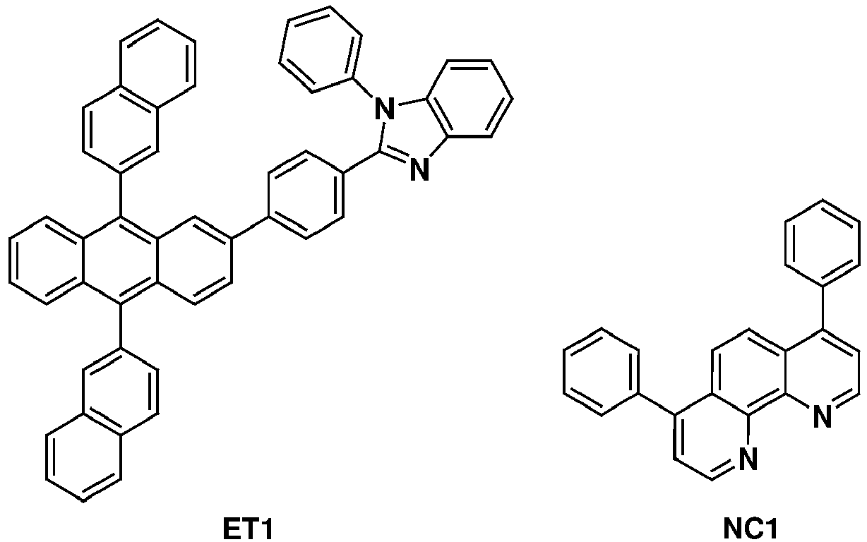

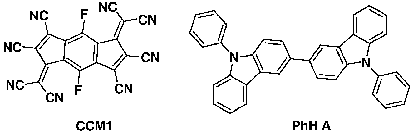

- In the above mentioned Embodiment 1, an organic electric element was manufactured in the same manner as in the Embodiment 1, except that the following CCM2 as the third compound was used instead of CCM1.

- The organic electric element was manufactured in the same manner as in the Embodiment 1, except that the following HI-01 as the third compound was used instead of CCM1.
- Table 1 shows the HOMO energy levels and LUMO energy levels of some of the compounds used in the Embodiments and Comparative Example.
[Table 1] HOMO (eV) LUMO (eV) PH1 -5.4 -2.4 PD1 - -5.25 HI-01 - -4.21 CCM1 - -5.02 CCM2 - -4.85 - Table 2 shows the performances of the manufactured organic electric elements in the Embodiments and Comparative Example.
[Table 2] First Layer driving voltage (ΔV) efficiency (sample/Ref, %) Lifespan (sample/Ref, %) General formula 1 (eV) General formula 2 (eV) General formula 3 (eV) Embodiment1 PH1 + PD1(5%) + CCM1(5%) -0.5V 102% 138% 0.23 2.62 0.38 Embodiment2 PH1 + PD1(5%) + CCM2(5%) -0.5V 102% 151% 0.4 2.45 0.55 Comparative Example 1 PH1+ PD1(5%) + HI-01(5%) +1.1V 84% 72% 1.04 1.81 1.19 - As can be seen from the result of the table 2, since the organic electric elements according to the embodiments 1 and 2 include the first layer including the first compound, the second compound and the third compound, they can have excellent efficiency and/or lifespan compared to the organic electric element of the Comparative Example 1.
- The above description has been presented to enable any person skilled in the art to make and use the technical idea of the present invention, and has been provided in the context of a particular application and its requirements. Various modifications, additions and substitutions to the described embodiments will be readily apparent to those skilled in the art, and the general principles defined herein can be applied to other embodiments and applications without departing from the scope of the present invention. The above description and the accompanying drawings provide an example of the technical idea of the present invention for illustrative purposes only.
- For example, the disclosed embodiments are intended to illustrate the scope of the technical idea of the present invention. Thus, the scope of the present invention is not limited to the embodiments shown, but is to be accorded the widest scope consistent with the claims. The scope of protection of the present invention should be construed based on the following claims.
Claims (15)
- An organic electric element (220, 320, 420) comprising:a first electrode (221, 321, 421);a second electrode (223, 323, 423); andan organic layer (222, 322, 422) positioned between the first electrode (221, 321, 421) and the second electrode (223, 323, 423), and comprising a first layer (222a, 322a, 422a) and a light emitting layer (222b, 322b, 422b),wherein the first layer (222a, 322a, 422a) comprises a first compound, a second compound, and a third compound, andthe first compound has a Highest Occupied Molecular Orbital, HOMO, energy level of -5.5eV to -5.0eV,the organic electric element (220, 320, 420) satisfies a following general formula 1:

- The organic electric element (220, 320, 420) according to claim 1, wherein the second compound and the third compound have the LUMO energy level of -4.0 eV or less, respectively.
- The organic electric element (220, 320, 420) according to claim 1 or 2, wherein the LUMO energy level of the third compound is greater than the HOMO energy level of the first compound.
- The organic electric element (220, 320, 420) according to any one of claims 1 to 3, wherein the first compound and the third compound included in the organic electric element (220, 320, 420) satisfy a following general formula 2:

- The organic electric element (220, 320, 420) according to any one of claims 1 to 4, wherein the first compound and the third compound included in the organic electric element (220, 320, 420) satisfy a following general formula 3:

- The organic electric element (220, 320, 420) according to any one of claims 1 to 5, wherein the first layer (222a, 322a, 422a) is positioned between the first electrode (221, 321, 421) and the light emitting layer (222b, 322b, 422b).
- The organic electric element (320, 420) according to any one of claims 1 to 5, wherein the organic layer (322, 422) comprises two or more light emitting layers (322b, 422b), and the first layer (322a, 422a) is positioned between the first electrode (321, 421) and one of the two or more light emitting layers (322b, 422b).
- The organic electric element (220, 320, 420) according to any one of claims 1 to 5, wherein the organic layer (322, 422) comprises two or more light emitting layers (322b, 422b), and the first layer (322a, 422a) is positioned between the light emitting layers (322b, 422b).
- The organic electric element (220, 320, 420) according to any one of claims 1 to 8, wherein the first compound includes a tertiary amine-based material.
- The organic electric element (220, 320, 420) according to any one of claims 1 to 9, wherein the second compound is a cyanocarbon-based material.
- The organic electric element (220, 320, 420) according to any one of claims 1 to 10, wherein the third compound includes an indacene-based material.
- The organic electric element (220, 320, 420) according to any one of claims 1 to 11, wherein a sum of a weight of the second compound and a weight of the third compound is approximately 0.1% to 50% by weight according to a total weight of the first compound, the second compound, and the third compound.
- The organic electric element (220, 320, 420) according to any one of claims 1 to 12, wherein a ratio of a weight of the second compound and a weight of the third compound included in the first layer (222a, 322a, 422a) is approximately (1:99) to (99:1).
- A display panel (110) comprising a plurality of subpixels (111), wherein each of at least one of the plurality of subpixels (111) comprises the organic electric element (220, 320, 420) of any one of claims 1 to 13.
- A display device (100) comprising;
the display panel (110) of claim 14; and
a driving circuit (GDC, DDC) configured to drive the display panel (110).
Applications Claiming Priority (1)
| Application Number | Priority Date | Filing Date | Title |
|---|---|---|---|
| KR1020190180033A KR102782422B1 (en) | 2019-12-31 | 2019-12-31 | Organic electronic element, display panel comprising the same and display device comprising the same |
Publications (2)
| Publication Number | Publication Date |
|---|---|
| EP3846233A1 true EP3846233A1 (en) | 2021-07-07 |
| EP3846233B1 EP3846233B1 (en) | 2025-12-03 |
Family
ID=73789900
Family Applications (1)
| Application Number | Title | Priority Date | Filing Date |
|---|---|---|---|
| EP20212711.4A Active EP3846233B1 (en) | 2019-12-31 | 2020-12-09 | Organic electric element, display panel comprising the same and display device comprising the same |
Country Status (4)
| Country | Link |
|---|---|
| US (1) | US11430964B2 (en) |
| EP (1) | EP3846233B1 (en) |
| KR (1) | KR102782422B1 (en) |
| CN (1) | CN113130797B (en) |
Citations (3)
| Publication number | Priority date | Publication date | Assignee | Title |
|---|---|---|---|---|
| GB2527606A (en) * | 2014-06-27 | 2015-12-30 | Cambridge Display Tech Ltd | Charge-transfer salt |
| US20170104172A1 (en) * | 2015-10-12 | 2017-04-13 | The Regents Of The University Of Michigan | Organic Light Emitting Diode Having a Mixed Blocking Layer |
| EP3176844A1 (en) * | 2015-12-03 | 2017-06-07 | LG Display Co., Ltd. | Organic light emitting display device |
Family Cites Families (3)
| Publication number | Priority date | Publication date | Assignee | Title |
|---|---|---|---|---|
| KR100922758B1 (en) * | 2008-02-20 | 2009-10-21 | 삼성모바일디스플레이주식회사 | Organic light emitting device |
| KR102279375B1 (en) * | 2015-12-03 | 2021-07-22 | 엘지디스플레이 주식회사 | Organic Light Emitting Diode Device |
| KR102620084B1 (en) * | 2016-07-29 | 2024-01-02 | 엘지디스플레이 주식회사 | Organic Light Emitting Element and Organic Light Emitting Display Device Using the Same |
-
2019
- 2019-12-31 KR KR1020190180033A patent/KR102782422B1/en active Active
-
2020
- 2020-12-09 EP EP20212711.4A patent/EP3846233B1/en active Active
- 2020-12-10 CN CN202011437647.2A patent/CN113130797B/en active Active
- 2020-12-29 US US17/136,784 patent/US11430964B2/en active Active
Patent Citations (3)
| Publication number | Priority date | Publication date | Assignee | Title |
|---|---|---|---|---|
| GB2527606A (en) * | 2014-06-27 | 2015-12-30 | Cambridge Display Tech Ltd | Charge-transfer salt |
| US20170104172A1 (en) * | 2015-10-12 | 2017-04-13 | The Regents Of The University Of Michigan | Organic Light Emitting Diode Having a Mixed Blocking Layer |
| EP3176844A1 (en) * | 2015-12-03 | 2017-06-07 | LG Display Co., Ltd. | Organic light emitting display device |
Non-Patent Citations (1)
| Title |
|---|
| YASUTAKA ENDO ET AL: "Synthesis and Electronic Structure of Dicyanofulvene-Fused Electron Accepting Molecule Based on a 1,5-Dihydro- s -Indacene Framework", ORGANIC LETTERS ., vol. 16, no. 21, 7 November 2014 (2014-11-07), US, pages 5608 - 5611, XP055365865, ISSN: 1523-7060, DOI: 10.1021/ol502675n * |
Also Published As
| Publication number | Publication date |
|---|---|
| EP3846233B1 (en) | 2025-12-03 |
| US11430964B2 (en) | 2022-08-30 |
| US20210202871A1 (en) | 2021-07-01 |
| KR102782422B1 (en) | 2025-03-18 |
| CN113130797A (en) | 2021-07-16 |
| CN113130797B (en) | 2024-04-05 |
| KR20210086232A (en) | 2021-07-08 |
Similar Documents
| Publication | Publication Date | Title |
|---|---|---|
| EP3846241A1 (en) | Organic electric element, display panel comprising the same and display device comprising the same | |
| US20240306489A1 (en) | Organic electric element, display panel comprising the same and display device comprising the same | |
| KR102512069B1 (en) | Blue organic light emitting device and display device including the same | |
| EP3846239B1 (en) | Organic electric element, display panel comprising the same and display device comprising the same | |
| US20240040812A1 (en) | Organic electric element, display panel comprising the same and display device comprising the same | |
| EP3846242B1 (en) | Organic electric element, display panel comprising the same and display device comprising the same | |
| US12349590B2 (en) | Organic electric element, display panel comprising the same and display device comprising the same | |
| EP3846233B1 (en) | Organic electric element, display panel comprising the same and display device comprising the same | |
| EP3846237B1 (en) | Organic electric element, display panel comprising the same and display device comprising the same | |
| US20230217809A1 (en) | Organic electronic element, display panel comprising the same and display device comprising the same |
Legal Events
| Date | Code | Title | Description |
|---|---|---|---|
| STAA | Information on the status of an ep patent application or granted ep patent |
Free format text: STATUS: REQUEST FOR EXAMINATION WAS MADE |
|
| PUAI | Public reference made under article 153(3) epc to a published international application that has entered the european phase |
Free format text: ORIGINAL CODE: 0009012 |
|
| 17P | Request for examination filed |
Effective date: 20201209 |
|
| AK | Designated contracting states |
Kind code of ref document: A1 Designated state(s): AL AT BE BG CH CY CZ DE DK EE ES FI FR GB GR HR HU IE IS IT LI LT LU LV MC MK MT NL NO PL PT RO RS SE SI SK SM TR |
|
| RBV | Designated contracting states (corrected) |
Designated state(s): AL AT BE BG CH CY CZ DE DK EE ES FI FR GB GR HR HU IE IS IT LI LT LU LV MC MK MT NL NO PL PT RO RS SE SI SK SM TR |
|
| STAA | Information on the status of an ep patent application or granted ep patent |
Free format text: STATUS: EXAMINATION IS IN PROGRESS |
|
| 17Q | First examination report despatched |
Effective date: 20230411 |
|
| REG | Reference to a national code |
Ref country code: DE Ref legal event code: R079 Free format text: PREVIOUS MAIN CLASS: H01L0051500000 Ipc: H10K0050155000 Ref country code: DE Ref legal event code: R079 Ref document number: 602020063129 Country of ref document: DE Free format text: PREVIOUS MAIN CLASS: H01L0051500000 Ipc: H10K0050155000 |
|
| GRAP | Despatch of communication of intention to grant a patent |
Free format text: ORIGINAL CODE: EPIDOSNIGR1 |
|
| STAA | Information on the status of an ep patent application or granted ep patent |
Free format text: STATUS: GRANT OF PATENT IS INTENDED |
|
| RIC1 | Information provided on ipc code assigned before grant |
Ipc: H10K 50/15 20230101ALI20250602BHEP Ipc: H10K 101/30 20230101ALI20250602BHEP Ipc: H10K 85/00 20230101ALI20250602BHEP Ipc: H10K 50/19 20230101ALI20250602BHEP Ipc: H10K 50/155 20230101AFI20250602BHEP |
|
| INTG | Intention to grant announced |
Effective date: 20250624 |
|
| GRAS | Grant fee paid |
Free format text: ORIGINAL CODE: EPIDOSNIGR3 |
|
| GRAA | (expected) grant |
Free format text: ORIGINAL CODE: 0009210 |
|
| STAA | Information on the status of an ep patent application or granted ep patent |
Free format text: STATUS: THE PATENT HAS BEEN GRANTED |
|
| AK | Designated contracting states |
Kind code of ref document: B1 Designated state(s): AL AT BE BG CH CY CZ DE DK EE ES FI FR GB GR HR HU IE IS IT LI LT LU LV MC MK MT NL NO PL PT RO RS SE SI SK SM TR |
|
| REG | Reference to a national code |
Ref country code: CH Ref legal event code: F10 Free format text: ST27 STATUS EVENT CODE: U-0-0-F10-F00 (AS PROVIDED BY THE NATIONAL OFFICE) Effective date: 20251203 Ref country code: GB Ref legal event code: FG4D |
|
| REG | Reference to a national code |
Ref country code: DE Ref legal event code: R096 Ref document number: 602020063129 Country of ref document: DE |
|
| REG | Reference to a national code |
Ref country code: IE Ref legal event code: FG4D |
|
| PGFP | Annual fee paid to national office [announced via postgrant information from national office to epo] |
Ref country code: FR Payment date: 20251230 Year of fee payment: 6 |
|
| REG | Reference to a national code |
Ref country code: NL Ref legal event code: MP Effective date: 20251203 |
|
| PGFP | Annual fee paid to national office [announced via postgrant information from national office to epo] |
Ref country code: GB Payment date: 20260108 Year of fee payment: 6 |
|
| PG25 | Lapsed in a contracting state [announced via postgrant information from national office to epo] |
Ref country code: ES Free format text: LAPSE BECAUSE OF FAILURE TO SUBMIT A TRANSLATION OF THE DESCRIPTION OR TO PAY THE FEE WITHIN THE PRESCRIBED TIME-LIMIT Effective date: 20251203 |
|
| REG | Reference to a national code |
Ref country code: LT Ref legal event code: MG9D |
|
| PG25 | Lapsed in a contracting state [announced via postgrant information from national office to epo] |
Ref country code: NO Free format text: LAPSE BECAUSE OF FAILURE TO SUBMIT A TRANSLATION OF THE DESCRIPTION OR TO PAY THE FEE WITHIN THE PRESCRIBED TIME-LIMIT Effective date: 20260303 |
|
| PGFP | Annual fee paid to national office [announced via postgrant information from national office to epo] |
Ref country code: DE Payment date: 20260105 Year of fee payment: 6 |
|
| PG25 | Lapsed in a contracting state [announced via postgrant information from national office to epo] |
Ref country code: HR Free format text: LAPSE BECAUSE OF FAILURE TO SUBMIT A TRANSLATION OF THE DESCRIPTION OR TO PAY THE FEE WITHIN THE PRESCRIBED TIME-LIMIT Effective date: 20251203 Ref country code: FI Free format text: LAPSE BECAUSE OF FAILURE TO SUBMIT A TRANSLATION OF THE DESCRIPTION OR TO PAY THE FEE WITHIN THE PRESCRIBED TIME-LIMIT Effective date: 20251203 |
|
| PG25 | Lapsed in a contracting state [announced via postgrant information from national office to epo] |
Ref country code: RS Free format text: LAPSE BECAUSE OF FAILURE TO SUBMIT A TRANSLATION OF THE DESCRIPTION OR TO PAY THE FEE WITHIN THE PRESCRIBED TIME-LIMIT Effective date: 20260303 |
|
| PG25 | Lapsed in a contracting state [announced via postgrant information from national office to epo] |
Ref country code: PL Free format text: LAPSE BECAUSE OF FAILURE TO SUBMIT A TRANSLATION OF THE DESCRIPTION OR TO PAY THE FEE WITHIN THE PRESCRIBED TIME-LIMIT Effective date: 20251203 |
|
| PG25 | Lapsed in a contracting state [announced via postgrant information from national office to epo] |
Ref country code: LV Free format text: LAPSE BECAUSE OF FAILURE TO SUBMIT A TRANSLATION OF THE DESCRIPTION OR TO PAY THE FEE WITHIN THE PRESCRIBED TIME-LIMIT Effective date: 20251203 |
|
| PG25 | Lapsed in a contracting state [announced via postgrant information from national office to epo] |
Ref country code: BG Free format text: LAPSE BECAUSE OF FAILURE TO SUBMIT A TRANSLATION OF THE DESCRIPTION OR TO PAY THE FEE WITHIN THE PRESCRIBED TIME-LIMIT Effective date: 20251203 |