EP3846224A1 - Deep trench and junction hybrid isolation - Google Patents
Deep trench and junction hybrid isolation Download PDFInfo
- Publication number
- EP3846224A1 EP3846224A1 EP20216887.8A EP20216887A EP3846224A1 EP 3846224 A1 EP3846224 A1 EP 3846224A1 EP 20216887 A EP20216887 A EP 20216887A EP 3846224 A1 EP3846224 A1 EP 3846224A1
- Authority
- EP
- European Patent Office
- Prior art keywords
- dti
- anode
- drain
- ldmos
- voltage potential
- Prior art date
- Legal status (The legal status is an assumption and is not a legal conclusion. Google has not performed a legal analysis and makes no representation as to the accuracy of the status listed.)
- Withdrawn
Links
Images




Classifications
-
- H—ELECTRICITY
- H10—SEMICONDUCTOR DEVICES; ELECTRIC SOLID-STATE DEVICES NOT OTHERWISE PROVIDED FOR
- H10D—INORGANIC ELECTRIC SEMICONDUCTOR DEVICES
- H10D84/00—Integrated devices formed in or on semiconductor substrates that comprise only semiconducting layers, e.g. on Si wafers or on GaAs-on-Si wafers
- H10D84/101—Integrated devices comprising main components and built-in components, e.g. IGBT having built-in freewheel diode
- H10D84/151—LDMOS having built-in components
- H10D84/153—LDMOS having built-in components the built-in component being PN junction diodes
-
- H—ELECTRICITY
- H10—SEMICONDUCTOR DEVICES; ELECTRIC SOLID-STATE DEVICES NOT OTHERWISE PROVIDED FOR
- H10D—INORGANIC ELECTRIC SEMICONDUCTOR DEVICES
- H10D30/00—Field-effect transistors [FET]
- H10D30/60—Insulated-gate field-effect transistors [IGFET]
- H10D30/64—Double-diffused metal-oxide semiconductor [DMOS] FETs
- H10D30/65—Lateral DMOS [LDMOS] FETs
-
- H—ELECTRICITY
- H10—SEMICONDUCTOR DEVICES; ELECTRIC SOLID-STATE DEVICES NOT OTHERWISE PROVIDED FOR
- H10D—INORGANIC ELECTRIC SEMICONDUCTOR DEVICES
- H10D8/00—Diodes
-
- H—ELECTRICITY
- H03—ELECTRONIC CIRCUITRY
- H03K—PULSE TECHNIQUE
- H03K17/00—Electronic switching or gating, i.e. not by contact-making and –breaking
- H03K17/10—Modifications for increasing the maximum permissible switched voltage
- H03K17/102—Modifications for increasing the maximum permissible switched voltage in field-effect transistor switches
-
- H—ELECTRICITY
- H10—SEMICONDUCTOR DEVICES; ELECTRIC SOLID-STATE DEVICES NOT OTHERWISE PROVIDED FOR
- H10D—INORGANIC ELECTRIC SEMICONDUCTOR DEVICES
- H10D30/00—Field-effect transistors [FET]
- H10D30/60—Insulated-gate field-effect transistors [IGFET]
- H10D30/601—Insulated-gate field-effect transistors [IGFET] having lightly-doped drain or source extensions, e.g. LDD IGFETs or DDD IGFETs
- H10D30/603—Insulated-gate field-effect transistors [IGFET] having lightly-doped drain or source extensions, e.g. LDD IGFETs or DDD IGFETs having asymmetry in the channel direction, e.g. lateral high-voltage MISFETs having drain offset region or extended drain IGFETs [EDMOS]
-
- H—ELECTRICITY
- H10—SEMICONDUCTOR DEVICES; ELECTRIC SOLID-STATE DEVICES NOT OTHERWISE PROVIDED FOR
- H10D—INORGANIC ELECTRIC SEMICONDUCTOR DEVICES
- H10D30/00—Field-effect transistors [FET]
- H10D30/60—Insulated-gate field-effect transistors [IGFET]
- H10D30/64—Double-diffused metal-oxide semiconductor [DMOS] FETs
- H10D30/65—Lateral DMOS [LDMOS] FETs
- H10D30/655—Lateral DMOS [LDMOS] FETs having edge termination structures
-
- H—ELECTRICITY
- H10—SEMICONDUCTOR DEVICES; ELECTRIC SOLID-STATE DEVICES NOT OTHERWISE PROVIDED FOR
- H10D—INORGANIC ELECTRIC SEMICONDUCTOR DEVICES
- H10D30/00—Field-effect transistors [FET]
- H10D30/60—Insulated-gate field-effect transistors [IGFET]
- H10D30/64—Double-diffused metal-oxide semiconductor [DMOS] FETs
- H10D30/65—Lateral DMOS [LDMOS] FETs
- H10D30/657—Lateral DMOS [LDMOS] FETs having substrates comprising insulating layers, e.g. SOI-LDMOS transistors
-
- H—ELECTRICITY
- H10—SEMICONDUCTOR DEVICES; ELECTRIC SOLID-STATE DEVICES NOT OTHERWISE PROVIDED FOR
- H10D—INORGANIC ELECTRIC SEMICONDUCTOR DEVICES
- H10D62/00—Semiconductor bodies, or regions thereof, of devices having potential barriers
- H10D62/10—Shapes, relative sizes or dispositions of the regions of the semiconductor bodies; Shapes of the semiconductor bodies
- H10D62/102—Constructional design considerations for preventing surface leakage or controlling electric field concentration
- H10D62/103—Constructional design considerations for preventing surface leakage or controlling electric field concentration for increasing or controlling the breakdown voltage of reverse-biased devices
- H10D62/105—Constructional design considerations for preventing surface leakage or controlling electric field concentration for increasing or controlling the breakdown voltage of reverse-biased devices by having particular doping profiles, shapes or arrangements of PN junctions; by having supplementary regions, e.g. junction termination extension [JTE]
- H10D62/106—Constructional design considerations for preventing surface leakage or controlling electric field concentration for increasing or controlling the breakdown voltage of reverse-biased devices by having particular doping profiles, shapes or arrangements of PN junctions; by having supplementary regions, e.g. junction termination extension [JTE] having supplementary regions doped oppositely to or in rectifying contact with regions of the semiconductor bodies, e.g. guard rings with PN or Schottky junctions
-
- H—ELECTRICITY
- H10—SEMICONDUCTOR DEVICES; ELECTRIC SOLID-STATE DEVICES NOT OTHERWISE PROVIDED FOR
- H10D—INORGANIC ELECTRIC SEMICONDUCTOR DEVICES
- H10D62/00—Semiconductor bodies, or regions thereof, of devices having potential barriers
- H10D62/10—Shapes, relative sizes or dispositions of the regions of the semiconductor bodies; Shapes of the semiconductor bodies
- H10D62/113—Isolations within a component, i.e. internal isolations
- H10D62/115—Dielectric isolations, e.g. air gaps
-
- H—ELECTRICITY
- H10—SEMICONDUCTOR DEVICES; ELECTRIC SOLID-STATE DEVICES NOT OTHERWISE PROVIDED FOR
- H10D—INORGANIC ELECTRIC SEMICONDUCTOR DEVICES
- H10D62/00—Semiconductor bodies, or regions thereof, of devices having potential barriers
- H10D62/10—Shapes, relative sizes or dispositions of the regions of the semiconductor bodies; Shapes of the semiconductor bodies
- H10D62/113—Isolations within a component, i.e. internal isolations
- H10D62/115—Dielectric isolations, e.g. air gaps
- H10D62/116—Dielectric isolations, e.g. air gaps adjoining the input or output regions of field-effect devices, e.g. adjoining source or drain regions
-
- H—ELECTRICITY
- H10—SEMICONDUCTOR DEVICES; ELECTRIC SOLID-STATE DEVICES NOT OTHERWISE PROVIDED FOR
- H10D—INORGANIC ELECTRIC SEMICONDUCTOR DEVICES
- H10D62/00—Semiconductor bodies, or regions thereof, of devices having potential barriers
- H10D62/10—Shapes, relative sizes or dispositions of the regions of the semiconductor bodies; Shapes of the semiconductor bodies
- H10D62/124—Shapes, relative sizes or dispositions of the regions of semiconductor bodies or of junctions between the regions
- H10D62/126—Top-view geometrical layouts of the regions or the junctions
-
- H—ELECTRICITY
- H10—SEMICONDUCTOR DEVICES; ELECTRIC SOLID-STATE DEVICES NOT OTHERWISE PROVIDED FOR
- H10D—INORGANIC ELECTRIC SEMICONDUCTOR DEVICES
- H10D62/00—Semiconductor bodies, or regions thereof, of devices having potential barriers
- H10D62/10—Shapes, relative sizes or dispositions of the regions of the semiconductor bodies; Shapes of the semiconductor bodies
- H10D62/13—Semiconductor regions connected to electrodes carrying current to be rectified, amplified or switched, e.g. source or drain regions
- H10D62/149—Source or drain regions of field-effect devices
- H10D62/151—Source or drain regions of field-effect devices of IGFETs
- H10D62/152—Source regions of DMOS transistors
- H10D62/154—Dispositions
-
- H—ELECTRICITY
- H10—SEMICONDUCTOR DEVICES; ELECTRIC SOLID-STATE DEVICES NOT OTHERWISE PROVIDED FOR
- H10D—INORGANIC ELECTRIC SEMICONDUCTOR DEVICES
- H10D62/00—Semiconductor bodies, or regions thereof, of devices having potential barriers
- H10D62/10—Shapes, relative sizes or dispositions of the regions of the semiconductor bodies; Shapes of the semiconductor bodies
- H10D62/13—Semiconductor regions connected to electrodes carrying current to be rectified, amplified or switched, e.g. source or drain regions
- H10D62/149—Source or drain regions of field-effect devices
- H10D62/151—Source or drain regions of field-effect devices of IGFETs
- H10D62/156—Drain regions of DMOS transistors
- H10D62/158—Dispositions
-
- H—ELECTRICITY
- H10—SEMICONDUCTOR DEVICES; ELECTRIC SOLID-STATE DEVICES NOT OTHERWISE PROVIDED FOR
- H10D—INORGANIC ELECTRIC SEMICONDUCTOR DEVICES
- H10D62/00—Semiconductor bodies, or regions thereof, of devices having potential barriers
- H10D62/10—Shapes, relative sizes or dispositions of the regions of the semiconductor bodies; Shapes of the semiconductor bodies
- H10D62/17—Semiconductor regions connected to electrodes not carrying current to be rectified, amplified or switched, e.g. channel regions
- H10D62/351—Substrate regions of field-effect devices
- H10D62/357—Substrate regions of field-effect devices of FETs
- H10D62/364—Substrate regions of field-effect devices of FETs of IGFETs
- H10D62/378—Contact regions to the substrate regions
-
- H—ELECTRICITY
- H10—SEMICONDUCTOR DEVICES; ELECTRIC SOLID-STATE DEVICES NOT OTHERWISE PROVIDED FOR
- H10D—INORGANIC ELECTRIC SEMICONDUCTOR DEVICES
- H10D62/00—Semiconductor bodies, or regions thereof, of devices having potential barriers
- H10D62/10—Shapes, relative sizes or dispositions of the regions of the semiconductor bodies; Shapes of the semiconductor bodies
- H10D62/17—Semiconductor regions connected to electrodes not carrying current to be rectified, amplified or switched, e.g. channel regions
- H10D62/393—Body regions of DMOS transistors or IGBTs
-
- H—ELECTRICITY
- H10—SEMICONDUCTOR DEVICES; ELECTRIC SOLID-STATE DEVICES NOT OTHERWISE PROVIDED FOR
- H10D—INORGANIC ELECTRIC SEMICONDUCTOR DEVICES
- H10D84/00—Integrated devices formed in or on semiconductor substrates that comprise only semiconducting layers, e.g. on Si wafers or on GaAs-on-Si wafers
- H10D84/101—Integrated devices comprising main components and built-in components, e.g. IGBT having built-in freewheel diode
- H10D84/151—LDMOS having built-in components
- H10D84/153—LDMOS having built-in components the built-in component being PN junction diodes
- H10D84/154—LDMOS having built-in components the built-in component being PN junction diodes in antiparallel diode configurations
-
- H—ELECTRICITY
- H10—SEMICONDUCTOR DEVICES; ELECTRIC SOLID-STATE DEVICES NOT OTHERWISE PROVIDED FOR
- H10D—INORGANIC ELECTRIC SEMICONDUCTOR DEVICES
- H10D84/00—Integrated devices formed in or on semiconductor substrates that comprise only semiconducting layers, e.g. on Si wafers or on GaAs-on-Si wafers
- H10D84/80—Integrated devices formed in or on semiconductor substrates that comprise only semiconducting layers, e.g. on Si wafers or on GaAs-on-Si wafers characterised by the integration of at least one component covered by groups H10D12/00 or H10D30/00, e.g. integration of IGFETs
- H10D84/82—Integrated devices formed in or on semiconductor substrates that comprise only semiconducting layers, e.g. on Si wafers or on GaAs-on-Si wafers characterised by the integration of at least one component covered by groups H10D12/00 or H10D30/00, e.g. integration of IGFETs of only field-effect components
- H10D84/83—Integrated devices formed in or on semiconductor substrates that comprise only semiconducting layers, e.g. on Si wafers or on GaAs-on-Si wafers characterised by the integration of at least one component covered by groups H10D12/00 or H10D30/00, e.g. integration of IGFETs of only field-effect components of only insulated-gate FETs [IGFET]
-
- H—ELECTRICITY
- H10—SEMICONDUCTOR DEVICES; ELECTRIC SOLID-STATE DEVICES NOT OTHERWISE PROVIDED FOR
- H10P—GENERIC PROCESSES OR APPARATUS FOR THE MANUFACTURE OR TREATMENT OF DEVICES COVERED BY CLASS H10
- H10P90/00—Preparation of wafers not covered by a single main group of this subclass, e.g. wafer reinforcement
- H10P90/19—Preparing inhomogeneous wafers
- H10P90/1904—Preparing vertically inhomogeneous wafers
- H10P90/1906—Preparing SOI wafers
-
- H—ELECTRICITY
- H10—SEMICONDUCTOR DEVICES; ELECTRIC SOLID-STATE DEVICES NOT OTHERWISE PROVIDED FOR
- H10W—GENERIC PACKAGES, INTERCONNECTIONS, CONNECTORS OR OTHER CONSTRUCTIONAL DETAILS OF DEVICES COVERED BY CLASS H10
- H10W10/00—Isolation regions in semiconductor bodies between components of integrated devices
- H10W10/01—Manufacture or treatment
- H10W10/011—Manufacture or treatment of isolation regions comprising dielectric materials
- H10W10/014—Manufacture or treatment of isolation regions comprising dielectric materials using trench refilling with dielectric materials, e.g. shallow trench isolations
-
- H—ELECTRICITY
- H10—SEMICONDUCTOR DEVICES; ELECTRIC SOLID-STATE DEVICES NOT OTHERWISE PROVIDED FOR
- H10W—GENERIC PACKAGES, INTERCONNECTIONS, CONNECTORS OR OTHER CONSTRUCTIONAL DETAILS OF DEVICES COVERED BY CLASS H10
- H10W10/00—Isolation regions in semiconductor bodies between components of integrated devices
- H10W10/01—Manufacture or treatment
- H10W10/011—Manufacture or treatment of isolation regions comprising dielectric materials
- H10W10/014—Manufacture or treatment of isolation regions comprising dielectric materials using trench refilling with dielectric materials, e.g. shallow trench isolations
- H10W10/0148—Manufacture or treatment of isolation regions comprising dielectric materials using trench refilling with dielectric materials, e.g. shallow trench isolations comprising introducing impurities in side walls or bottom walls of trenches, e.g. for forming channel stoppers
-
- H—ELECTRICITY
- H10—SEMICONDUCTOR DEVICES; ELECTRIC SOLID-STATE DEVICES NOT OTHERWISE PROVIDED FOR
- H10W—GENERIC PACKAGES, INTERCONNECTIONS, CONNECTORS OR OTHER CONSTRUCTIONAL DETAILS OF DEVICES COVERED BY CLASS H10
- H10W10/00—Isolation regions in semiconductor bodies between components of integrated devices
- H10W10/01—Manufacture or treatment
- H10W10/061—Manufacture or treatment using SOI processes together with lateral isolation, e.g. combinations of SOI and shallow trench isolations
-
- H—ELECTRICITY
- H10—SEMICONDUCTOR DEVICES; ELECTRIC SOLID-STATE DEVICES NOT OTHERWISE PROVIDED FOR
- H10W—GENERIC PACKAGES, INTERCONNECTIONS, CONNECTORS OR OTHER CONSTRUCTIONAL DETAILS OF DEVICES COVERED BY CLASS H10
- H10W10/00—Isolation regions in semiconductor bodies between components of integrated devices
- H10W10/10—Isolation regions comprising dielectric materials
- H10W10/17—Isolation regions comprising dielectric materials formed using trench refilling with dielectric materials, e.g. shallow trench isolations
-
- H—ELECTRICITY
- H10—SEMICONDUCTOR DEVICES; ELECTRIC SOLID-STATE DEVICES NOT OTHERWISE PROVIDED FOR
- H10W—GENERIC PACKAGES, INTERCONNECTIONS, CONNECTORS OR OTHER CONSTRUCTIONAL DETAILS OF DEVICES COVERED BY CLASS H10
- H10W10/00—Isolation regions in semiconductor bodies between components of integrated devices
- H10W10/10—Isolation regions comprising dielectric materials
- H10W10/181—Semiconductor-on-insulator [SOI] isolation regions, e.g. buried oxide regions of SOI wafers
-
- H—ELECTRICITY
- H10—SEMICONDUCTOR DEVICES; ELECTRIC SOLID-STATE DEVICES NOT OTHERWISE PROVIDED FOR
- H10D—INORGANIC ELECTRIC SEMICONDUCTOR DEVICES
- H10D62/00—Semiconductor bodies, or regions thereof, of devices having potential barriers
- H10D62/10—Shapes, relative sizes or dispositions of the regions of the semiconductor bodies; Shapes of the semiconductor bodies
- H10D62/124—Shapes, relative sizes or dispositions of the regions of semiconductor bodies or of junctions between the regions
- H10D62/126—Top-view geometrical layouts of the regions or the junctions
- H10D62/127—Top-view geometrical layouts of the regions or the junctions of cellular field-effect devices, e.g. multicellular DMOS transistors or IGBTs
-
- H—ELECTRICITY
- H10—SEMICONDUCTOR DEVICES; ELECTRIC SOLID-STATE DEVICES NOT OTHERWISE PROVIDED FOR
- H10D—INORGANIC ELECTRIC SEMICONDUCTOR DEVICES
- H10D64/00—Electrodes of devices having potential barriers
- H10D64/111—Field plates
-
- H—ELECTRICITY
- H10—SEMICONDUCTOR DEVICES; ELECTRIC SOLID-STATE DEVICES NOT OTHERWISE PROVIDED FOR
- H10W—GENERIC PACKAGES, INTERCONNECTIONS, CONNECTORS OR OTHER CONSTRUCTIONAL DETAILS OF DEVICES COVERED BY CLASS H10
- H10W10/00—Isolation regions in semiconductor bodies between components of integrated devices
- H10W10/01—Manufacture or treatment
- H10W10/031—Manufacture or treatment of isolation regions comprising PN junctions
-
- H—ELECTRICITY
- H10—SEMICONDUCTOR DEVICES; ELECTRIC SOLID-STATE DEVICES NOT OTHERWISE PROVIDED FOR
- H10W—GENERIC PACKAGES, INTERCONNECTIONS, CONNECTORS OR OTHER CONSTRUCTIONAL DETAILS OF DEVICES COVERED BY CLASS H10
- H10W10/00—Isolation regions in semiconductor bodies between components of integrated devices
- H10W10/30—Isolation regions comprising PN junctions
Definitions
- This disclosure relates generally to high voltage semiconductor devices, and more specifically to increasing an operating and isolation voltage of a Laterally Diffused Metal Oxide Semiconductor (LDMOS) and circuit block.
- LDMOS Laterally Diffused Metal Oxide Semiconductor
- LDMOS devices are frequently used in high voltage applications (e.g., automotive applications), requiring high voltage under high-side operation. Such devices are also being used with the requirement of high voltage isolation between circuitry, with increasing demanding high voltage levels.
- SOI Silicon-On-Insulator
- DTI Deep Trench Isolation
- the isolation voltage is limited by a Buried Oxide (BOX) thickness and a DTI sidewall oxide thickness. While, it is relatively simple to increase the BOX thickness, increasing the DTI sidewall thickness involves additional process complexity, which could lead to higher mechanical stress and thus higher defectivity levels.
- a hybrid isolation structure consisting of a DTI and a biased junction isolation is used to increase the voltage isolation of a circuit beyond what is achievable by using a DTI without further enhancement. Accordingly, an isolation and a maximum operating voltage are increased without incurring additional process complexity, cost or an increase of defectivity levels, (for example due to dislocation faults).
- a drain of an LDMOS is biased with a high voltage potential, being higher in voltage than a low voltage potential.
- a DTI laterally surrounds the LDMOS, and a bulk, source and gate terminal of the LDMOS are each connected to the low voltage potential (e.g., "ground” or 0V).
- the drain connects to a drift region of the LDMOS.
- the source connects to a body region of the LDMOS.
- Equipotential electric field lines define a voltage gradient between the drain and at least one other electrical net comprising the source terminal.
- bias voltage potential By contacting the drift region with a reverse biased diode connection, outside of the conduction path between the source and the drain, at a location corresponding to a specific equipotential field line, a bias voltage potential, (or "bias potential"), is extracted.
- the bias voltage is chosen to correspond to a voltage being less than a maximum allowed voltage across a sidewall of the DTI, by adjusting a distance between the drain and the diode connection to the drift region.
- the choice of the field line corresponding to the bias voltage is further defined with a high voltage p-type implant between the cathode of the diode and the drift region.
- the bias voltage capacitively charges the anode of the diode, which in further connected to a p-type region, (or a region having the same doping polarity as the anode), proximate to the DTI, thereby pinning the DTI sidewall voltage to prevent damage to the DTI from the higher operating voltage of the drain.
- FIG. 1 is a partial plan view of an example embodiment 10 of a DTI and junction hybrid isolation apparatus.
- a high voltage n-type LDMOS (NLD) 12 extracts the bias voltage by aligning a location of a diode with a specific equipotential field line.
- a DTI and junction hybrid isolation structure 14 receives the bias voltage and provides a region for additional circuitry to operate (or be isolated) from a high voltage, otherwise exceeding the normal operating limits of the DTI.
- the NLD 12 includes a pair of drains 20 and 22. In one example embodiment of an NLD 12, the drains 20 and 22 connect to a drift region formed by a high voltage n-type (HVN) region 24.
- HVN high voltage n-type
- the HVN region 24 is separated from a p-type high voltage (PHV) region 26 by an epitaxial region 28.
- the HVN region 24 comprises the drift region.
- the PHV region 26 comprises the body region.
- a first DTI 30 laterally surrounds the PHV region 26 and thus the high voltage NLD device 12.
- a p-plus region 32 forms an anode of a diode, whose cathode, (not shown), connects to the drift region.
- a high voltage p-type (HVP) region is formed between the cathode of the diode and the drift region.
- a second DTI 40 is electrically connected to the first DTI 30.
- a p-plus region 42 is laterally surrounded by the second DTI 40.
- an HVP region 43 is formed under the p-plus region 42.
- an n-type isolation ring 44 is formed within an NHV region 45 to isolate circuitry laterally enclosed therein.
- the isolation ring 44 is separated from the p-plus region 42 by an epitaxial region 46.
- a length and/or width of the isolation ring 44 are adjusted dependent upon the shape and size of the various circuits in the region 48, within the isolation ring 44.
- FIG. 2 is a cross-section view of a deep trench and junction hybrid isolation apparatus, in accordance with an example embodiment 50 of the present disclosure.
- the example embodiment 50 comprises an NLD device 52, an extracted high voltage supply 54 and a DTI and junction hybrid isolation structure 56.
- the example embodiment 50 is formed on an n-type substrate 60, covered with a BOX layer 62.
- a DTI consisting of doped polysilicon 64 and sidewall oxide 66 on either side of the polysilicon, is formed to contact the n-type substrate 60.
- the DTI 64 + 66
- An epitaxial layer 68 is formed over the BOX 62 for the NLD device 52.
- a PHV region 70 is formed in the epitaxial layer 68, comprising the body region of the NLD device 52.
- a p-plus region 72 forms a bulk contact to the body region.
- An n-plus region 74 forms a source contact to the body region.
- an n-type lightly doped source implant 76 is formed adjacent to the source contact.
- a shallow trench isolation (STI) 78 separates the bulk contact from the DTI sidewall oxide 66.
- An HVN region 80 is formed in the epitaxial layer 68, comprising the drift region of the NLD device 52.
- An n-plus implant 82 forms a drain contact in the HVN 80.
- An STI 84 and an STI 86 are formed on either side of the drain contact.
- a polysilicon gate 88 is formed over the body and drift regions to enable the formation of a conduction channel of the NLD device 52.
- an interconnect 90 connects the DTI 64, the bulk and source contacts, the polysilicon gate 88, and the metal field plate 92 to a low voltage potential (e.g., ground).
- a p-type implant 94 forms an anode of a diode with the HVN 80 forming the cathode. In some embodiments, the anode is separated from the HVN 80 by an HVP 96 implant.
- a lightly doped n-type buried layer (LNBL) 100 is formed over the BOX 62 in the DTI and junction hybrid isolation region 56. The epitaxial layer 68 is formed over the LNBL 100.
- An n-type high voltage region (NHV) 102 is formed over the LNBL 100.
- a p-type implant 104 forms a shield junction in the DTI and junction hybrid isolation structure 56.
- An STI 106 and an STI 108 are formed on either side of the shield junction.
- an HVP 110 is formed under the p-plus implant 104.
- An n-plus implant 112 forms a high voltage isolation ring in the NHV 102.
- An interlayer dielectric 114 covers the active structures of the example embodiment 50.
- the drain of the NLD device 52 is connected to the high voltage isolation ring and to a high voltage supply with an interconnect 116, depicted symbolically for clarity of illustration.
- the anode of the diode in the NLD device 52 is connected to the shield junction with an interconnect 118, depicted symbolically for clarity of illustration.
- the interconnect 116 and 118 are formed with metal interconnect similar to the shown interconnect line 90.
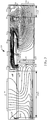
- FIG. 3 shows an example embodiment 120 of an electrostatic potential profile of the structure of FIG. 2 , wherein the gate 88, source 74, bulk 72, DTI 64 and substrate 60 are biased to the low voltage potential, and the drain 82 is biased to the high voltage potential.
- the example embodiment 120 includes conductors 122, 124 and 128 connecting to the drain, source (and body) and high voltage isolation ring as respectively shown in FIG. 2 .
- the example embodiment 120 includes a conductor 126, similar to the symbolic conductor 118 of FIG. 2 , for connecting the anode to the shield junction.
- a plurality of equipotential field lines 130 defining a voltage gradient between the drain at 82 and at least one other electrical net comprising the source at 74.
- the drain is biased to a high voltage and the source is biased to a low voltage (e.g., 0V).
- the equipotential field lines emanate from the drain at 82 towards lower voltage conductors, including the source, bulk and gate.
- the drain 20 corresponding to the drain at 82 in FIG. 3
- the drain 22 are equally spaced from the anode at 94.
- the equipotential field lines tend to be parallel to the BOX or to the surface below the drain of the example embodiment 120, but change direction between the drain and the anode at 94.
- a specific equipotential field line 134 will intersect the anode and thereby cause the anode to be charged to a bias voltage potential.
- the first distance 132 is further adjusted by the introduction of the HVP implant 96 of FIG. 2 .
- the bias voltage potential is chosen to be less than a maximum allowed voltage across a sidewall 66 of the second DTI 64 + 66 (or 40 of FIG. 1 ). Accordingly, the DTI sidewall 66 is shielded by the shield junction 104 to prevent the DTI sidewall 66 from being exposed to the higher voltage applied to the drain of the example embodiment 120.
- An additional set of equipotential field lines 136 define a voltage gradient emanating from the high voltage isolation ring at 112.
- the high voltage isolation ring at 112 is separated from the shield junction at 104 by a second distance 138 to minimize the disturbance of the equipotential field lines 136 on the field line 134.
- the second distance 138 divided by the first distance 132 should have a ratio of 3:1 or within a range of 2:1 to 6:1, to minimize adverse effects on the bias voltage.
- FIG. 4 shows the breakdown characteristics of the NLD device 52 of FIG.2 .
- the breakdown voltage (BVdss) 140 of the NLD device 52 is shown at 140V, above the high side operating voltage of 120V applied to the drain at 82.
- BVdss breakdown voltage
- a bias voltage potential of 79V is applied to the shield junction, while the drain at 82 is biased to the high voltage potential of 120V.
- FIG. 6 shows a method 160 for improving the deep trench and junction hybrid isolation in accordance with an example embodiment of the present disclosure.
- an LDMOS Drain at 82 is biased to a high voltage (e.g., 120V in FIG. 5 ).
- An LDMOS source is biased to a low voltage (e.g., 0V).
- Equipotential field lines 130 define a voltage gradient between the drain at 82 and at least one net comprising the source at 74.
- an anode at 94, of a diode is charged to a bias potential (79V in FIG. 5 ), by displacing the anode from the drain (by a distance 132), to intersect the equipotential field line 134 corresponding to the bias potential.
- the LDMOS is isolated with a DTI (64 + 66, or 30 in FIG. 1 ), proximate to the LDMOS source at 74.
- the DTI 64 + 66 or 30
- the DTI is shielded with a shield junction at 104, connected to the anode at 94.
- an apparatus comprises a Laterally Diffused Metal Oxide Semiconductor (LDMOS) comprising a drain connected to a drift region and a source connected to a body region. The body region is laterally separated from the drift region.
- the drain is connectable to a high voltage potential
- the source is connectable to a low voltage potential.
- a diode comprises an anode and a cathode. The cathode is electrically coupled to the drift region, wherein during an operating condition, the anode is capacitively charged to a bias voltage potential, wherein the bias voltage potential is less than the high voltage potential applied to the drain and greater than the low voltage potential applied to the source.
- the anode is laterally displaced from the drain by a first distance.
- a first deep trench isolation (DTI) is disposed to laterally surround the LDMOS.
- the first DTI is proximate to the source.
- a shield junction comprises a same doping polarity as the anode and is disposed proximate to the first DTI and on an opposite side of the source, wherein the shield junction is electrically connected to the anode.
- the first DTI is electrically connected to a second DTI, the second DTI disposed to laterally surround the shield junction, and the shield junction disposed to laterally surround a circuit.
- the bias voltage potential is less than a maximum allowed voltage across a sidewall of the second DTI.
- the maximum allowed voltage of the second DTI is less than an LDMOS breakdown voltage of the LDMOS.
- a high voltage isolation ring connected to the high voltage potential is laterally displaced from the shield junction by a second distance, wherein the second distance is greater than the first distance.
- the LDMOS is an n-type Field Effect Transistor.
- the LDMOS is a p-type Field Effect Transistor.
- the DTI is electrically connected to a second DTI, the second DTI disposed to laterally surround a circuit.
- a high voltage p-type implant is between the cathode and the drift region.
- a second drain is laterally displaced from the anode by the first distance, the second drain connectable to the high voltage potential.
- a method for deep trench and junction hybrid isolation comprises biasing a Laterally Diffused Metal Oxide Semiconductor (LDMOS), comprising biasing a drain connected to a drift region to a high voltage potential and biasing a source connected to a body region to a low voltage potential.
- An anode of a diode is charged to a bias voltage potential, wherein a cathode of the diode is electrically coupled to the drift region.
- the bias voltage potential is less than the high voltage potential and greater than the low voltage potential, and the anode laterally displaced from the drain by a first distance.
- the LDMOS is electrically isolated with a first deep trench isolation (DTI) disposed to laterally surround the LDMOS.
- the first DTI is proximate to the source.
- the first DTI is shielded with a shield junction disposed proximate to the first DTI, wherein the shield junction is electrically connected to the anode.
- DTI deep trench isolation
- the first DTI is electrically connected to a second DTI, wherein the second DTI is disposed to laterally surround the shield junction, and the shield junction is disposed to laterally surround a circuit.
- the bias voltage potential is less than a maximum allowed voltage across a sidewall of the second DTI.
- the maximum allowed voltage of the second DTI is less than an LDMOS breakdown voltage of the LDMOS.
- a high voltage isolation ring is laterally displaced from the shield junction by a second distance, wherein the second distance is greater than the first distance.
- the cathode is separated from the drift region with a high voltage p-type implant.
- a second drain is laterally displaced from the anode by the first distance, wherein the second drain is connected to the high voltage potential.
- an apparatus comprises a first Field Effect Transistor (FET) comprising a drain connected to a drift region and a source connected to a body region, the drain connectable to a high voltage potential, the source connectable to a low voltage potential.
- FET Field Effect Transistor
- a diode comprises an anode and a cathode, the cathode electrically coupled to the drift region, and the anode laterally displaced from the drain by a first distance.
- a first deep trench isolation (DTI) is disposed to laterally surround the first FET, the first DTI proximate to the source.
- a second DTI is electrically connected to the first DTI, wherein the second DTI is disposed to laterally surround a circuit.
- a shield junction comprises a same doping polarity as the anode and is disposed proximate to the first DTI and laterally surrounded by the second DTI, wherein the shield junction is electrically connected to the anode.
- a high voltage p-type implant is between the cathode and the drift region.
- a second drain is laterally displaced from the anode by the first distance, the second drain connected to the high voltage potential.
Landscapes
- Insulated Gate Type Field-Effect Transistor (AREA)
- Metal-Oxide And Bipolar Metal-Oxide Semiconductor Integrated Circuits (AREA)
Abstract
An apparatus comprises a Laterally Diffused Metal Oxide Semiconductor (LDMOS) comprising a drain connectable to a drift region and a source connectable to a body region. A diode comprises a cathode electrically coupled to the drift region, wherein during an operating condition, the anode is charged to a bias voltage less than a high voltage applied to the drain and greater than a low voltage applied to the source. The anode is laterally displaced from the drain by a first distance. A first deep trench isolation (DTI) is proximate to the source and disposed to laterally surround the LDMOS. A shield junction is proximate to the first DTI and on an opposite side of the source, and electrically connected to the anode.
Description
- This disclosure relates generally to high voltage semiconductor devices, and more specifically to increasing an operating and isolation voltage of a Laterally Diffused Metal Oxide Semiconductor (LDMOS) and circuit block.
- LDMOS devices are frequently used in high voltage applications (e.g., automotive applications), requiring high voltage under high-side operation. Such devices are also being used with the requirement of high voltage isolation between circuitry, with increasing demanding high voltage levels. In particular, for Silicon-On-Insulator (SOI) technology with a Deep Trench Isolation (DTI), the isolation voltage is limited by a Buried Oxide (BOX) thickness and a DTI sidewall oxide thickness. While, it is relatively simple to increase the BOX thickness, increasing the DTI sidewall thickness involves additional process complexity, which could lead to higher mechanical stress and thus higher defectivity levels.
- The present invention is illustrated by way of example and is not limited by the accompanying figures, in which like references indicate similar elements. Elements in the figures are illustrated for simplicity and clarity and have not necessarily been drawn to scale.
-
FIG. 1 is a partial plan view of a deep trench and junction hybrid isolation apparatus, in accordance with an example embodiment of the present disclosure. -
FIG. 2 is a cross-section view of a deep trench and junction hybrid isolation apparatus, in accordance with an example embodiment of the present disclosure. -
FIG. 3 is an example embodiment of an electrostatic potential profile ofFIG. 2 , showing equipotential field lines at the breakdown condition of a hybrid isolation structure. -
FIG. 4 is a graphical view showing a breakdown characteristic of an LDMOS, in accordance with an example embodiment of the present disclosure. -
FIG. 5 is a graphical view of a bias voltage potential derived from the apparatus ofFIG. 2 , in accordance with an example embodiment of the present disclosure. -
FIG. 6 is a flowchart representation of a method for deep trench and junction hybrid isolation in accordance with an example embodiment of the present disclosure. - Various embodiments described herein provide for improving high voltage isolation using a DTI and junction hybrid isolation structure. A hybrid isolation structure consisting of a DTI and a biased junction isolation is used to increase the voltage isolation of a circuit beyond what is achievable by using a DTI without further enhancement. Accordingly, an isolation and a maximum operating voltage are increased without incurring additional process complexity, cost or an increase of defectivity levels, (for example due to dislocation faults).
- During one operating condition, a drain of an LDMOS is biased with a high voltage potential, being higher in voltage than a low voltage potential. In one example embodiment, a DTI laterally surrounds the LDMOS, and a bulk, source and gate terminal of the LDMOS are each connected to the low voltage potential (e.g., "ground" or 0V). The drain connects to a drift region of the LDMOS. The source connects to a body region of the LDMOS. Equipotential electric field lines define a voltage gradient between the drain and at least one other electrical net comprising the source terminal. By contacting the drift region with a reverse biased diode connection, outside of the conduction path between the source and the drain, at a location corresponding to a specific equipotential field line, a bias voltage potential, (or "bias potential"), is extracted. The bias voltage is chosen to correspond to a voltage being less than a maximum allowed voltage across a sidewall of the DTI, by adjusting a distance between the drain and the diode connection to the drift region. In another example embodiment, the choice of the field line corresponding to the bias voltage is further defined with a high voltage p-type implant between the cathode of the diode and the drift region. The bias voltage capacitively charges the anode of the diode, which in further connected to a p-type region, (or a region having the same doping polarity as the anode), proximate to the DTI, thereby pinning the DTI sidewall voltage to prevent damage to the DTI from the higher operating voltage of the drain.
-
FIG. 1 is a partial plan view of anexample embodiment 10 of a DTI and junction hybrid isolation apparatus. A high voltage n-type LDMOS (NLD) 12 extracts the bias voltage by aligning a location of a diode with a specific equipotential field line. A DTI and junctionhybrid isolation structure 14 receives the bias voltage and provides a region for additional circuitry to operate (or be isolated) from a high voltage, otherwise exceeding the normal operating limits of the DTI. The NLD 12 includes a pair ofdrains NLD 12, thedrains epitaxial region 28. The HVN region 24 comprises the drift region. The PHV region 26 comprises the body region. Afirst DTI 30 laterally surrounds the PHV region 26 and thus the highvoltage NLD device 12. A p-plus region 32 forms an anode of a diode, whose cathode, (not shown), connects to the drift region. In some embodiments, a high voltage p-type (HVP) region is formed between the cathode of the diode and the drift region. - A second DTI 40 is electrically connected to the
first DTI 30. A p-plus region 42 is laterally surrounded by thesecond DTI 40. In one embodiment, an HVP region 43 is formed under the p-plus region 42. In one embodiment, an n-type isolation ring 44 is formed within anNHV region 45 to isolate circuitry laterally enclosed therein. Theisolation ring 44 is separated from the p-plus region 42 by anepitaxial region 46. In one embodiment, a length and/or width of theisolation ring 44 are adjusted dependent upon the shape and size of the various circuits in theregion 48, within theisolation ring 44. -
FIG. 2 is a cross-section view of a deep trench and junction hybrid isolation apparatus, in accordance with anexample embodiment 50 of the present disclosure. Theexample embodiment 50 comprises anNLD device 52, an extractedhigh voltage supply 54 and a DTI and junctionhybrid isolation structure 56. Theexample embodiment 50 is formed on an n-type substrate 60, covered with aBOX layer 62. A DTI, consisting of doped polysilicon 64 andsidewall oxide 66 on either side of the polysilicon, is formed to contact the n-type substrate 60. In one embodiment, the DTI (64 + 66) comprises a portion of both thefirst DTI 30 and thesecond DTI 40 ofFIG. 1 . Anepitaxial layer 68 is formed over theBOX 62 for theNLD device 52. APHV region 70 is formed in theepitaxial layer 68, comprising the body region of theNLD device 52. A p-plus region 72 forms a bulk contact to the body region. An n-plus region 74 forms a source contact to the body region. In some embodiments, an n-type lightly dopedsource implant 76 is formed adjacent to the source contact. A shallow trench isolation (STI) 78 separates the bulk contact from theDTI sidewall oxide 66. - An
HVN region 80 is formed in theepitaxial layer 68, comprising the drift region of theNLD device 52. An n-plus implant 82 forms a drain contact in the HVN 80. An STI 84 and an STI 86 are formed on either side of the drain contact. Apolysilicon gate 88 is formed over the body and drift regions to enable the formation of a conduction channel of theNLD device 52. In one embodiment of theNLD device 52 configured for use in high voltage isolation, aninterconnect 90 connects the DTI 64, the bulk and source contacts, thepolysilicon gate 88, and themetal field plate 92 to a low voltage potential (e.g., ground). - A p-
type implant 94 forms an anode of a diode with theHVN 80 forming the cathode. In some embodiments, the anode is separated from theHVN 80 by anHVP 96 implant. A lightly doped n-type buried layer (LNBL) 100 is formed over theBOX 62 in the DTI and junctionhybrid isolation region 56. Theepitaxial layer 68 is formed over theLNBL 100. An n-type high voltage region (NHV) 102 is formed over theLNBL 100. A p-type implant 104 forms a shield junction in the DTI and junctionhybrid isolation structure 56. AnSTI 106 and anSTI 108 are formed on either side of the shield junction. In one embodiment, anHVP 110 is formed under the p-plus implant 104. - An n-
plus implant 112 forms a high voltage isolation ring in theNHV 102. Aninterlayer dielectric 114 covers the active structures of theexample embodiment 50. The drain of theNLD device 52 is connected to the high voltage isolation ring and to a high voltage supply with an interconnect 116, depicted symbolically for clarity of illustration. The anode of the diode in theNLD device 52 is connected to the shield junction with aninterconnect 118, depicted symbolically for clarity of illustration. In one embodiment, theinterconnect 116 and 118 are formed with metal interconnect similar to the showninterconnect line 90. -
FIG. 3 shows anexample embodiment 120 of an electrostatic potential profile of the structure ofFIG. 2 , wherein thegate 88,source 74,bulk 72, DTI 64 andsubstrate 60 are biased to the low voltage potential, and thedrain 82 is biased to the high voltage potential. Theexample embodiment 120 includesconductors FIG. 2 . Theexample embodiment 120 includes aconductor 126, similar to thesymbolic conductor 118 ofFIG. 2 , for connecting the anode to the shield junction. A plurality ofequipotential field lines 130 defining a voltage gradient between the drain at 82 and at least one other electrical net comprising the source at 74. For clarity of illustration, not all field lines have been shown. In theexample embodiment 120, the drain is biased to a high voltage and the source is biased to a low voltage (e.g., 0V). The equipotential field lines emanate from the drain at 82 towards lower voltage conductors, including the source, bulk and gate. As shown inFIG. 1 , the drain 20 (corresponding to the drain at 82 inFIG. 3 ) and thedrain 22 are equally spaced from the anode at 94. The equipotential field lines tend to be parallel to the BOX or to the surface below the drain of theexample embodiment 120, but change direction between the drain and the anode at 94. - By separating the anode at 94 from the drain at 82, by a
first distance 132, a specificequipotential field line 134 will intersect the anode and thereby cause the anode to be charged to a bias voltage potential. In one embodiment, thefirst distance 132 is further adjusted by the introduction of theHVP implant 96 ofFIG. 2 . The bias voltage potential is chosen to be less than a maximum allowed voltage across asidewall 66 of the second DTI 64 + 66 (or 40 ofFIG. 1 ). Accordingly, theDTI sidewall 66 is shielded by theshield junction 104 to prevent theDTI sidewall 66 from being exposed to the higher voltage applied to the drain of theexample embodiment 120. - An additional set of
equipotential field lines 136 define a voltage gradient emanating from the high voltage isolation ring at 112. In one embodiment, the high voltage isolation ring at 112 is separated from the shield junction at 104 by asecond distance 138 to minimize the disturbance of theequipotential field lines 136 on thefield line 134. In practice, thesecond distance 138 divided by thefirst distance 132 should have a ratio of 3:1 or within a range of 2:1 to 6:1, to minimize adverse effects on the bias voltage. -
FIG. 4 shows the breakdown characteristics of theNLD device 52 ofFIG.2 . In the example embodiment ofFIG. 4 , the breakdown voltage (BVdss) 140 of theNLD device 52 is shown at 140V, above the high side operating voltage of 120V applied to the drain at 82. In the example embodiment ofFIG. 5 , a bias voltage potential of 79V is applied to the shield junction, while the drain at 82 is biased to the high voltage potential of 120V. -
FIG. 6 , with ongoing reference toFIG. 2 ,FIG. 3 andFIG. 5 shows amethod 160 for improving the deep trench and junction hybrid isolation in accordance with an example embodiment of the present disclosure. At 162 ("Biasing an LDMOS Drain connected to a drift region to a high voltage, and an LDMOS source to a low voltage, wherein equipotential field lines define a voltage gradient between the drain and at least one net comprising the source"), an LDMOS Drain at 82, connected to a drift region, is biased to a high voltage (e.g., 120V inFIG. 5 ). An LDMOS source is biased to a low voltage (e.g., 0V).Equipotential field lines 130 define a voltage gradient between the drain at 82 and at least one net comprising the source at 74. At 164 ("charging an anode of a diode to a bias potential by displacing the anode from the drain to intersect the equipotential field line corresponding to the bias potential"), an anode at 94, of a diode is charged to a bias potential (79V inFIG. 5 ), by displacing the anode from the drain (by a distance 132), to intersect theequipotential field line 134 corresponding to the bias potential. At 166 ("isolating the LDMOS with a DTI approximate to the LDMOS source"), the LDMOS is isolated with a DTI (64 + 66, or 30 inFIG. 1 ), proximate to the LDMOS source at 74. At 168 ("shielding the DTI with a shield junction connected to the anode"), the DTI (64 + 66 or 30) is shielded with a shield junction at 104, connected to the anode at 94. - As will be appreciated, embodiments as disclosed include at least the following. In one embodiment, an apparatus comprises a Laterally Diffused Metal Oxide Semiconductor (LDMOS) comprising a drain connected to a drift region and a source connected to a body region. The body region is laterally separated from the drift region. The drain is connectable to a high voltage potential, and the source is connectable to a low voltage potential. A diode comprises an anode and a cathode. The cathode is electrically coupled to the drift region, wherein during an operating condition, the anode is capacitively charged to a bias voltage potential, wherein the bias voltage potential is less than the high voltage potential applied to the drain and greater than the low voltage potential applied to the source. The anode is laterally displaced from the drain by a first distance. A first deep trench isolation (DTI) is disposed to laterally surround the LDMOS. The first DTI is proximate to the source. A shield junction comprises a same doping polarity as the anode and is disposed proximate to the first DTI and on an opposite side of the source, wherein the shield junction is electrically connected to the anode.
- Alternative embodiments of the apparatus include one of the following features, or any combination thereof. The first DTI is electrically connected to a second DTI, the second DTI disposed to laterally surround the shield junction, and the shield junction disposed to laterally surround a circuit. The bias voltage potential is less than a maximum allowed voltage across a sidewall of the second DTI. The maximum allowed voltage of the second DTI is less than an LDMOS breakdown voltage of the LDMOS. A high voltage isolation ring connected to the high voltage potential is laterally displaced from the shield junction by a second distance, wherein the second distance is greater than the first distance. The LDMOS is an n-type Field Effect Transistor. The LDMOS is a p-type Field Effect Transistor. The DTI is electrically connected to a second DTI, the second DTI disposed to laterally surround a circuit. A high voltage p-type implant is between the cathode and the drift region. A second drain is laterally displaced from the anode by the first distance, the second drain connectable to the high voltage potential.
- In another embodiment, a method for deep trench and junction hybrid isolation comprises biasing a Laterally Diffused Metal Oxide Semiconductor (LDMOS), comprising biasing a drain connected to a drift region to a high voltage potential and biasing a source connected to a body region to a low voltage potential. An anode of a diode is charged to a bias voltage potential, wherein a cathode of the diode is electrically coupled to the drift region. The bias voltage potential is less than the high voltage potential and greater than the low voltage potential, and the anode laterally displaced from the drain by a first distance. The LDMOS is electrically isolated with a first deep trench isolation (DTI) disposed to laterally surround the LDMOS. The first DTI is proximate to the source. The first DTI is shielded with a shield junction disposed proximate to the first DTI, wherein the shield junction is electrically connected to the anode.
- Alternative embodiments of the method for deep trench and junction hybrid isolation include one of the following features, or any combination thereof. The first DTI is electrically connected to a second DTI, wherein the second DTI is disposed to laterally surround the shield junction, and the shield junction is disposed to laterally surround a circuit. The bias voltage potential is less than a maximum allowed voltage across a sidewall of the second DTI. The maximum allowed voltage of the second DTI is less than an LDMOS breakdown voltage of the LDMOS. A high voltage isolation ring is laterally displaced from the shield junction by a second distance, wherein the second distance is greater than the first distance. The cathode is separated from the drift region with a high voltage p-type implant. A second drain is laterally displaced from the anode by the first distance, wherein the second drain is connected to the high voltage potential.
- In another embodiment, an apparatus comprises a first Field Effect Transistor (FET) comprising a drain connected to a drift region and a source connected to a body region, the drain connectable to a high voltage potential, the source connectable to a low voltage potential. A diode comprises an anode and a cathode, the cathode electrically coupled to the drift region, and the anode laterally displaced from the drain by a first distance. A first deep trench isolation (DTI) is disposed to laterally surround the first FET, the first DTI proximate to the source. A second DTI is electrically connected to the first DTI, wherein the second DTI is disposed to laterally surround a circuit. A shield junction comprises a same doping polarity as the anode and is disposed proximate to the first DTI and laterally surrounded by the second DTI, wherein the shield junction is electrically connected to the anode.
- Alternative embodiments of the apparatus include one of the following features, or any combination thereof. A high voltage p-type implant is between the cathode and the drift region. A second drain is laterally displaced from the anode by the first distance, the second drain connected to the high voltage potential.
- Although the invention is described herein with reference to specific embodiments, various modifications and changes can be made without departing from the scope of the present invention as set forth in the claims below. Accordingly, the specification and figures are to be regarded in an illustrative rather than a restrictive sense, and all such modifications are intended to be included within the scope of the present invention. Any benefits, advantages, or solutions to problems that are described herein with regard to specific embodiments are not intended to be construed as a critical, required, or essential feature or element of any or all the claims.
- Unless stated otherwise, terms such as "first" and "second" are used to arbitrarily distinguish between the elements such terms describe. Thus, these terms are not necessarily intended to indicate temporal or other prioritization of such elements.
Claims (15)
- An apparatus comprising:a Laterally Diffused Metal Oxide Semiconductor, LDMOS, comprising a drain connected to a drift region and a source connected to a body region, the body region laterally separated from the drift region, the drain connectable to a high voltage potential, the source connectable to a low voltage potential;a diode comprising an anode and a cathode, the cathode electrically coupled to the drift region, wherein during an operating condition, the anode capacitively charged to a bias voltage potential, wherein the bias voltage potential is less than the high voltage potential applied to the drain and greater than the low voltage potential applied to the source, and the anode laterally displaced from the drain by a first distance;a first deep trench isolation, DTI, disposed to laterally surround the LDMOS, the first DTI proximate to the source; anda shield junction comprising a same doping polarity as the anode and disposed proximate to the first DTI and on an opposite side of the source, wherein the shield junction is electrically connected to the anode.
- The apparatus of claim 1 wherein the first DTI is electrically connected to a second DTI, the second DTI disposed to laterally surround the shield junction, and the shield junction disposed to laterally surround a circuit.
- The apparatus of claim 2 wherein the bias voltage potential is less than a maximum allowed voltage across a sidewall of the second DTI.
- The apparatus of claim 3 wherein the maximum allowed voltage of the second DTI is less than an LDMOS breakdown voltage of the LDMOS.
- The apparatus of any preceding claim wherein a high voltage isolation ring connected to the high voltage potential is laterally displaced from the shield junction by a second distance, wherein the second distance is greater than the first distance.
- The apparatus of any preceding claim wherein the LDMOS is an n-type Field Effect Transistor.
- The apparatus of any preceding claim wherein the DTI is electrically connected to a second DTI, the second DTI disposed to laterally surround a circuit.
- The apparatus of any preceding claim further comprising a high voltage p-type implant between the cathode and the drift region.
- The apparatus of any preceding claim further comprising a second drain laterally displaced from the anode by the first distance, the second drain connectable to the high voltage potential.
- A method for deep trench and junction hybrid isolation comprising:biasing a Laterally Diffused Metal Oxide Semiconductor, LDMOS, comprising biasing a drain connected to a drift region to a high voltage potential and biasing a source connected to a body region to a low voltage potential;charging an anode of a diode to a bias voltage potential, wherein a cathode of the diode is electrically coupled to the drift region, the bias voltage potential is less than the high voltage potential and greater than the low voltage potential, and the anode laterally displaced from the drain by a first distance;electrically isolating the LDMOS with a first deep trench isolation, DTI, disposed to laterally surround the LDMOS, the first DTI proximate to the source; andshielding the first DTI with a shield junction disposed proximate to the first DTI, wherein the shield junction is electrically connected to the anode.
- The method of claim 10 further comprising electrically connecting the first DTI to a second DTI, wherein the second DTI is disposed to laterally surround the shield junction, and the shield junction is disposed to laterally surround a circuit.
- The method of claim 11 wherein the bias voltage potential is less than a maximum allowed voltage across a sidewall of the second DTI.
- The method of claim 12 wherein the maximum allowed voltage of the second DTI is less than an LDMOS breakdown voltage of the LDMOS.
- The method of any of claims 10 to 13 further comprising laterally displacing a high voltage isolation ring from the shield junction by a second distance, wherein the second distance is greater than the first distance.
- The method of any of claims 10 to 14 further comprising separating the cathode from the drift region with a high voltage p-type implant.
Applications Claiming Priority (1)
| Application Number | Priority Date | Filing Date | Title |
|---|---|---|---|
| US16/735,029 US10944001B1 (en) | 2020-01-06 | 2020-01-06 | Deep trench and junction hybrid isolation |
Publications (1)
| Publication Number | Publication Date |
|---|---|
| EP3846224A1 true EP3846224A1 (en) | 2021-07-07 |
Family
ID=73857035
Family Applications (1)
| Application Number | Title | Priority Date | Filing Date |
|---|---|---|---|
| EP20216887.8A Withdrawn EP3846224A1 (en) | 2020-01-06 | 2020-12-23 | Deep trench and junction hybrid isolation |
Country Status (3)
| Country | Link |
|---|---|
| US (1) | US10944001B1 (en) |
| EP (1) | EP3846224A1 (en) |
| CN (1) | CN113078219A (en) |
Families Citing this family (4)
| Publication number | Priority date | Publication date | Assignee | Title |
|---|---|---|---|---|
| US10971632B2 (en) * | 2019-06-24 | 2021-04-06 | Semiconductor Components Industries, Llc | High voltage diode on SOI substrate with trench-modified current path |
| CN115274859B (en) * | 2022-09-30 | 2023-01-20 | 北京芯可鉴科技有限公司 | LDMOS transistor and manufacturing method thereof |
| US20240162345A1 (en) * | 2022-11-10 | 2024-05-16 | Globalfoundries U.S. Inc. | Transistor with metal field plate contact |
| CN118825010A (en) * | 2023-04-21 | 2024-10-22 | 扬智科技股份有限公司 | Electrostatic discharge protection device |
Citations (1)
| Publication number | Priority date | Publication date | Assignee | Title |
|---|---|---|---|---|
| US20170110446A1 (en) * | 2015-10-15 | 2017-04-20 | United Microelectronics Corp. | Electrostatic discharge protection semiconductor device |
Family Cites Families (4)
| Publication number | Priority date | Publication date | Assignee | Title |
|---|---|---|---|---|
| EP2006900B1 (en) | 2007-05-25 | 2020-11-18 | Semiconductor Components Industries, LLC | Deep trench isolation for power semiconductors |
| US8541862B2 (en) | 2011-11-30 | 2013-09-24 | Freescale Semiconductor, Inc. | Semiconductor device with self-biased isolation |
| US9343526B2 (en) | 2013-03-13 | 2016-05-17 | Freescale Semiconductor, Inc. | Deep trench isolation |
| JP6971877B2 (en) * | 2018-02-20 | 2021-11-24 | ルネサスエレクトロニクス株式会社 | Semiconductor device |
-
2020
- 2020-01-06 US US16/735,029 patent/US10944001B1/en active Active
- 2020-12-23 EP EP20216887.8A patent/EP3846224A1/en not_active Withdrawn
-
2021
- 2021-01-06 CN CN202110010939.6A patent/CN113078219A/en active Pending
Patent Citations (1)
| Publication number | Priority date | Publication date | Assignee | Title |
|---|---|---|---|---|
| US20170110446A1 (en) * | 2015-10-15 | 2017-04-20 | United Microelectronics Corp. | Electrostatic discharge protection semiconductor device |
Also Published As
| Publication number | Publication date |
|---|---|
| CN113078219A (en) | 2021-07-06 |
| US10944001B1 (en) | 2021-03-09 |
Similar Documents
| Publication | Publication Date | Title |
|---|---|---|
| US10944001B1 (en) | Deep trench and junction hybrid isolation | |
| US9159803B2 (en) | Semiconductor device with HCI protection region | |
| US8445960B2 (en) | Self-aligned body fully isolated device | |
| US8338872B2 (en) | Electronic device with capcitively coupled floating buried layer | |
| US8476684B2 (en) | Field effect transistors having improved breakdown voltages and methods of forming the same | |
| US20130270606A1 (en) | Semiconductor Device with Integrated Breakdown Protection | |
| CN107768423B (en) | Lateral Diffused Metal Oxide Semiconductor Field Effect Transistor with Isolation Region | |
| US11329156B2 (en) | Transistor with extended drain region | |
| EP1378009A2 (en) | Field-effect transistor structure and method of manufacture | |
| US9508845B1 (en) | LDMOS device with high-potential-biased isolation ring | |
| US7074681B2 (en) | Semiconductor component and method of manufacturing | |
| US10217828B1 (en) | Transistors with field plates on fully depleted silicon-on-insulator platform and method of making the same | |
| US7521741B2 (en) | Shielding structures for preventing leakages in high voltage MOS devices | |
| US10256340B2 (en) | High-voltage semiconductor device and method for manufacturing the same | |
| EP3961722A1 (en) | Apparatus for extension of operation voltage | |
| US9412863B2 (en) | Enhanced breakdown voltages for high voltage MOSFETS | |
| EP3723136A1 (en) | Ldmos with diode coupled isolation ring | |
| EP4057360A1 (en) | Ldmos with an improved breakdown performance | |
| US11211449B2 (en) | Semiconductor device | |
| EP3599645A1 (en) | Semiconductor device with drain active area | |
| US20200357755A1 (en) | Transistors with electrically active chip seal ring and methods of manufacture | |
| US20250311361A1 (en) | Semiconductor device | |
| CN109216453B (en) | High-voltage semiconductor device and method of manufacturing the same | |
| CN121924795A (en) | Semiconductor device and method for manufacturing the same | |
| EP3261126B1 (en) | High-voltage semiconductor device and method for manufacturing the same |
Legal Events
| Date | Code | Title | Description |
|---|---|---|---|
| PUAI | Public reference made under article 153(3) epc to a published international application that has entered the european phase |
Free format text: ORIGINAL CODE: 0009012 |
|
| STAA | Information on the status of an ep patent application or granted ep patent |
Free format text: STATUS: THE APPLICATION HAS BEEN PUBLISHED |
|
| AK | Designated contracting states |
Kind code of ref document: A1 Designated state(s): AL AT BE BG CH CY CZ DE DK EE ES FI FR GB GR HR HU IE IS IT LI LT LU LV MC MK MT NL NO PL PT RO RS SE SI SK SM TR |
|
| STAA | Information on the status of an ep patent application or granted ep patent |
Free format text: STATUS: THE APPLICATION IS DEEMED TO BE WITHDRAWN |
|
| 18D | Application deemed to be withdrawn |
Effective date: 20220108 |