EP3845957A1 - Light control device and method for producing light control device - Google Patents
Light control device and method for producing light control device Download PDFInfo
- Publication number
- EP3845957A1 EP3845957A1 EP19855617.7A EP19855617A EP3845957A1 EP 3845957 A1 EP3845957 A1 EP 3845957A1 EP 19855617 A EP19855617 A EP 19855617A EP 3845957 A1 EP3845957 A1 EP 3845957A1
- Authority
- EP
- European Patent Office
- Prior art keywords
- light control
- transparent
- transparent adhesive
- coating substrate
- layer
- Prior art date
- Legal status (The legal status is an assumption and is not a legal conclusion. Google has not performed a legal analysis and makes no representation as to the accuracy of the status listed.)
- Withdrawn
Links
Images


Classifications
-
- G—PHYSICS
- G02—OPTICS
- G02F—OPTICAL DEVICES OR ARRANGEMENTS FOR THE CONTROL OF LIGHT BY MODIFICATION OF THE OPTICAL PROPERTIES OF THE MEDIA OF THE ELEMENTS INVOLVED THEREIN; NON-LINEAR OPTICS; FREQUENCY-CHANGING OF LIGHT; OPTICAL LOGIC ELEMENTS; OPTICAL ANALOGUE/DIGITAL CONVERTERS
- G02F1/00—Devices or arrangements for the control of the intensity, colour, phase, polarisation or direction of light arriving from an independent light source, e.g. switching, gating or modulating; Non-linear optics
- G02F1/01—Devices or arrangements for the control of the intensity, colour, phase, polarisation or direction of light arriving from an independent light source, e.g. switching, gating or modulating; Non-linear optics for the control of the intensity, phase, polarisation or colour
- G02F1/13—Devices or arrangements for the control of the intensity, colour, phase, polarisation or direction of light arriving from an independent light source, e.g. switching, gating or modulating; Non-linear optics for the control of the intensity, phase, polarisation or colour based on liquid crystals, e.g. single liquid crystal display cells
- G02F1/133—Constructional arrangements; Operation of liquid crystal cells; Circuit arrangements
- G02F1/1333—Constructional arrangements; Manufacturing methods
- G02F1/1343—Electrodes
- G02F1/13439—Electrodes characterised by their electrical, optical, physical properties; materials therefor; method of making
-
- B—PERFORMING OPERATIONS; TRANSPORTING
- B32—LAYERED PRODUCTS
- B32B—LAYERED PRODUCTS, i.e. PRODUCTS BUILT-UP OF STRATA OF FLAT OR NON-FLAT, e.g. CELLULAR OR HONEYCOMB, FORM
- B32B17/00—Layered products essentially comprising sheet glass, or glass, slag, or like fibres
- B32B17/06—Layered products essentially comprising sheet glass, or glass, slag, or like fibres comprising glass as the main or only constituent of a layer, next to another layer of a specific material
- B32B17/10—Layered products essentially comprising sheet glass, or glass, slag, or like fibres comprising glass as the main or only constituent of a layer, next to another layer of a specific material of synthetic resin
-
- B—PERFORMING OPERATIONS; TRANSPORTING
- B32—LAYERED PRODUCTS
- B32B—LAYERED PRODUCTS, i.e. PRODUCTS BUILT-UP OF STRATA OF FLAT OR NON-FLAT, e.g. CELLULAR OR HONEYCOMB, FORM
- B32B27/00—Layered products comprising a layer of synthetic resin
- B32B27/06—Layered products comprising a layer of synthetic resin as the main or only constituent of a layer, which is next to another layer of the same or of a different material
- B32B27/08—Layered products comprising a layer of synthetic resin as the main or only constituent of a layer, which is next to another layer of the same or of a different material of synthetic resin
-
- B—PERFORMING OPERATIONS; TRANSPORTING
- B32—LAYERED PRODUCTS
- B32B—LAYERED PRODUCTS, i.e. PRODUCTS BUILT-UP OF STRATA OF FLAT OR NON-FLAT, e.g. CELLULAR OR HONEYCOMB, FORM
- B32B27/00—Layered products comprising a layer of synthetic resin
- B32B27/30—Layered products comprising a layer of synthetic resin comprising vinyl (co)polymers; comprising acrylic (co)polymers
- B32B27/302—Layered products comprising a layer of synthetic resin comprising vinyl (co)polymers; comprising acrylic (co)polymers comprising aromatic vinyl (co)polymers, e.g. styrenic (co)polymers
-
- B—PERFORMING OPERATIONS; TRANSPORTING
- B32—LAYERED PRODUCTS
- B32B—LAYERED PRODUCTS, i.e. PRODUCTS BUILT-UP OF STRATA OF FLAT OR NON-FLAT, e.g. CELLULAR OR HONEYCOMB, FORM
- B32B27/00—Layered products comprising a layer of synthetic resin
- B32B27/30—Layered products comprising a layer of synthetic resin comprising vinyl (co)polymers; comprising acrylic (co)polymers
- B32B27/308—Layered products comprising a layer of synthetic resin comprising vinyl (co)polymers; comprising acrylic (co)polymers comprising acrylic (co)polymers
-
- B—PERFORMING OPERATIONS; TRANSPORTING
- B32—LAYERED PRODUCTS
- B32B—LAYERED PRODUCTS, i.e. PRODUCTS BUILT-UP OF STRATA OF FLAT OR NON-FLAT, e.g. CELLULAR OR HONEYCOMB, FORM
- B32B27/00—Layered products comprising a layer of synthetic resin
- B32B27/32—Layered products comprising a layer of synthetic resin comprising polyolefins
-
- B—PERFORMING OPERATIONS; TRANSPORTING
- B32—LAYERED PRODUCTS
- B32B—LAYERED PRODUCTS, i.e. PRODUCTS BUILT-UP OF STRATA OF FLAT OR NON-FLAT, e.g. CELLULAR OR HONEYCOMB, FORM
- B32B27/00—Layered products comprising a layer of synthetic resin
- B32B27/34—Layered products comprising a layer of synthetic resin comprising polyamides
-
- B—PERFORMING OPERATIONS; TRANSPORTING
- B32—LAYERED PRODUCTS
- B32B—LAYERED PRODUCTS, i.e. PRODUCTS BUILT-UP OF STRATA OF FLAT OR NON-FLAT, e.g. CELLULAR OR HONEYCOMB, FORM
- B32B27/00—Layered products comprising a layer of synthetic resin
- B32B27/36—Layered products comprising a layer of synthetic resin comprising polyesters
-
- B—PERFORMING OPERATIONS; TRANSPORTING
- B32—LAYERED PRODUCTS
- B32B—LAYERED PRODUCTS, i.e. PRODUCTS BUILT-UP OF STRATA OF FLAT OR NON-FLAT, e.g. CELLULAR OR HONEYCOMB, FORM
- B32B27/00—Layered products comprising a layer of synthetic resin
- B32B27/36—Layered products comprising a layer of synthetic resin comprising polyesters
- B32B27/365—Layered products comprising a layer of synthetic resin comprising polyesters comprising polycarbonates
-
- B—PERFORMING OPERATIONS; TRANSPORTING
- B32—LAYERED PRODUCTS
- B32B—LAYERED PRODUCTS, i.e. PRODUCTS BUILT-UP OF STRATA OF FLAT OR NON-FLAT, e.g. CELLULAR OR HONEYCOMB, FORM
- B32B27/00—Layered products comprising a layer of synthetic resin
- B32B27/40—Layered products comprising a layer of synthetic resin comprising polyurethanes
-
- B—PERFORMING OPERATIONS; TRANSPORTING
- B32—LAYERED PRODUCTS
- B32B—LAYERED PRODUCTS, i.e. PRODUCTS BUILT-UP OF STRATA OF FLAT OR NON-FLAT, e.g. CELLULAR OR HONEYCOMB, FORM
- B32B3/00—Layered products comprising a layer with external or internal discontinuities or unevennesses, or a layer of non-planar shape; Layered products comprising a layer having particular features of form
- B32B3/02—Layered products comprising a layer with external or internal discontinuities or unevennesses, or a layer of non-planar shape; Layered products comprising a layer having particular features of form characterised by features of form at particular places, e.g. in edge regions
-
- B—PERFORMING OPERATIONS; TRANSPORTING
- B32—LAYERED PRODUCTS
- B32B—LAYERED PRODUCTS, i.e. PRODUCTS BUILT-UP OF STRATA OF FLAT OR NON-FLAT, e.g. CELLULAR OR HONEYCOMB, FORM
- B32B7/00—Layered products characterised by the relation between layers; Layered products characterised by the relative orientation of features between layers, or by the relative values of a measurable parameter between layers, i.e. products comprising layers having different physical, chemical or physicochemical properties; Layered products characterised by the interconnection of layers
- B32B7/04—Interconnection of layers
- B32B7/12—Interconnection of layers using interposed adhesives or interposed materials with bonding properties
-
- G—PHYSICS
- G02—OPTICS
- G02F—OPTICAL DEVICES OR ARRANGEMENTS FOR THE CONTROL OF LIGHT BY MODIFICATION OF THE OPTICAL PROPERTIES OF THE MEDIA OF THE ELEMENTS INVOLVED THEREIN; NON-LINEAR OPTICS; FREQUENCY-CHANGING OF LIGHT; OPTICAL LOGIC ELEMENTS; OPTICAL ANALOGUE/DIGITAL CONVERTERS
- G02F1/00—Devices or arrangements for the control of the intensity, colour, phase, polarisation or direction of light arriving from an independent light source, e.g. switching, gating or modulating; Non-linear optics
- G02F1/01—Devices or arrangements for the control of the intensity, colour, phase, polarisation or direction of light arriving from an independent light source, e.g. switching, gating or modulating; Non-linear optics for the control of the intensity, phase, polarisation or colour
- G02F1/13—Devices or arrangements for the control of the intensity, colour, phase, polarisation or direction of light arriving from an independent light source, e.g. switching, gating or modulating; Non-linear optics for the control of the intensity, phase, polarisation or colour based on liquid crystals, e.g. single liquid crystal display cells
- G02F1/133—Constructional arrangements; Operation of liquid crystal cells; Circuit arrangements
- G02F1/1333—Constructional arrangements; Manufacturing methods
-
- G—PHYSICS
- G02—OPTICS
- G02F—OPTICAL DEVICES OR ARRANGEMENTS FOR THE CONTROL OF LIGHT BY MODIFICATION OF THE OPTICAL PROPERTIES OF THE MEDIA OF THE ELEMENTS INVOLVED THEREIN; NON-LINEAR OPTICS; FREQUENCY-CHANGING OF LIGHT; OPTICAL LOGIC ELEMENTS; OPTICAL ANALOGUE/DIGITAL CONVERTERS
- G02F1/00—Devices or arrangements for the control of the intensity, colour, phase, polarisation or direction of light arriving from an independent light source, e.g. switching, gating or modulating; Non-linear optics
- G02F1/01—Devices or arrangements for the control of the intensity, colour, phase, polarisation or direction of light arriving from an independent light source, e.g. switching, gating or modulating; Non-linear optics for the control of the intensity, phase, polarisation or colour
- G02F1/13—Devices or arrangements for the control of the intensity, colour, phase, polarisation or direction of light arriving from an independent light source, e.g. switching, gating or modulating; Non-linear optics for the control of the intensity, phase, polarisation or colour based on liquid crystals, e.g. single liquid crystal display cells
- G02F1/133—Constructional arrangements; Operation of liquid crystal cells; Circuit arrangements
- G02F1/1333—Constructional arrangements; Manufacturing methods
- G02F1/1334—Constructional arrangements; Manufacturing methods based on polymer dispersed liquid crystals, e.g. microencapsulated liquid crystals
-
- G—PHYSICS
- G02—OPTICS
- G02F—OPTICAL DEVICES OR ARRANGEMENTS FOR THE CONTROL OF LIGHT BY MODIFICATION OF THE OPTICAL PROPERTIES OF THE MEDIA OF THE ELEMENTS INVOLVED THEREIN; NON-LINEAR OPTICS; FREQUENCY-CHANGING OF LIGHT; OPTICAL LOGIC ELEMENTS; OPTICAL ANALOGUE/DIGITAL CONVERTERS
- G02F1/00—Devices or arrangements for the control of the intensity, colour, phase, polarisation or direction of light arriving from an independent light source, e.g. switching, gating or modulating; Non-linear optics
- G02F1/01—Devices or arrangements for the control of the intensity, colour, phase, polarisation or direction of light arriving from an independent light source, e.g. switching, gating or modulating; Non-linear optics for the control of the intensity, phase, polarisation or colour
- G02F1/13—Devices or arrangements for the control of the intensity, colour, phase, polarisation or direction of light arriving from an independent light source, e.g. switching, gating or modulating; Non-linear optics for the control of the intensity, phase, polarisation or colour based on liquid crystals, e.g. single liquid crystal display cells
- G02F1/133—Constructional arrangements; Operation of liquid crystal cells; Circuit arrangements
- G02F1/1333—Constructional arrangements; Manufacturing methods
- G02F1/1334—Constructional arrangements; Manufacturing methods based on polymer dispersed liquid crystals, e.g. microencapsulated liquid crystals
- G02F1/13345—Network or three-dimensional gels
-
- G—PHYSICS
- G02—OPTICS
- G02F—OPTICAL DEVICES OR ARRANGEMENTS FOR THE CONTROL OF LIGHT BY MODIFICATION OF THE OPTICAL PROPERTIES OF THE MEDIA OF THE ELEMENTS INVOLVED THEREIN; NON-LINEAR OPTICS; FREQUENCY-CHANGING OF LIGHT; OPTICAL LOGIC ELEMENTS; OPTICAL ANALOGUE/DIGITAL CONVERTERS
- G02F1/00—Devices or arrangements for the control of the intensity, colour, phase, polarisation or direction of light arriving from an independent light source, e.g. switching, gating or modulating; Non-linear optics
- G02F1/01—Devices or arrangements for the control of the intensity, colour, phase, polarisation or direction of light arriving from an independent light source, e.g. switching, gating or modulating; Non-linear optics for the control of the intensity, phase, polarisation or colour
- G02F1/13—Devices or arrangements for the control of the intensity, colour, phase, polarisation or direction of light arriving from an independent light source, e.g. switching, gating or modulating; Non-linear optics for the control of the intensity, phase, polarisation or colour based on liquid crystals, e.g. single liquid crystal display cells
- G02F1/133—Constructional arrangements; Operation of liquid crystal cells; Circuit arrangements
- G02F1/1333—Constructional arrangements; Manufacturing methods
- G02F1/1339—Gaskets; Spacers; Sealing of cells
- G02F1/13392—Gaskets; Spacers; Sealing of cells spacers dispersed on the cell substrate, e.g. spherical particles, microfibres
-
- G—PHYSICS
- G02—OPTICS
- G02F—OPTICAL DEVICES OR ARRANGEMENTS FOR THE CONTROL OF LIGHT BY MODIFICATION OF THE OPTICAL PROPERTIES OF THE MEDIA OF THE ELEMENTS INVOLVED THEREIN; NON-LINEAR OPTICS; FREQUENCY-CHANGING OF LIGHT; OPTICAL LOGIC ELEMENTS; OPTICAL ANALOGUE/DIGITAL CONVERTERS
- G02F1/00—Devices or arrangements for the control of the intensity, colour, phase, polarisation or direction of light arriving from an independent light source, e.g. switching, gating or modulating; Non-linear optics
- G02F1/01—Devices or arrangements for the control of the intensity, colour, phase, polarisation or direction of light arriving from an independent light source, e.g. switching, gating or modulating; Non-linear optics for the control of the intensity, phase, polarisation or colour
- G02F1/13—Devices or arrangements for the control of the intensity, colour, phase, polarisation or direction of light arriving from an independent light source, e.g. switching, gating or modulating; Non-linear optics for the control of the intensity, phase, polarisation or colour based on liquid crystals, e.g. single liquid crystal display cells
- G02F1/133—Constructional arrangements; Operation of liquid crystal cells; Circuit arrangements
- G02F1/1333—Constructional arrangements; Manufacturing methods
- G02F1/1339—Gaskets; Spacers; Sealing of cells
- G02F1/13398—Spacer materials; Spacer properties
-
- G—PHYSICS
- G02—OPTICS
- G02F—OPTICAL DEVICES OR ARRANGEMENTS FOR THE CONTROL OF LIGHT BY MODIFICATION OF THE OPTICAL PROPERTIES OF THE MEDIA OF THE ELEMENTS INVOLVED THEREIN; NON-LINEAR OPTICS; FREQUENCY-CHANGING OF LIGHT; OPTICAL LOGIC ELEMENTS; OPTICAL ANALOGUE/DIGITAL CONVERTERS
- G02F2201/00—Constructional arrangements not provided for in groups G02F1/00 - G02F7/00
- G02F2201/50—Protective arrangements
-
- G—PHYSICS
- G02—OPTICS
- G02F—OPTICAL DEVICES OR ARRANGEMENTS FOR THE CONTROL OF LIGHT BY MODIFICATION OF THE OPTICAL PROPERTIES OF THE MEDIA OF THE ELEMENTS INVOLVED THEREIN; NON-LINEAR OPTICS; FREQUENCY-CHANGING OF LIGHT; OPTICAL LOGIC ELEMENTS; OPTICAL ANALOGUE/DIGITAL CONVERTERS
- G02F2202/00—Materials and properties
- G02F2202/28—Adhesive materials or arrangements
Definitions
- the present invention relates to a light control device including a light control sheet and a method for producing the same.
- Alight control sheet includes a first electrode layer, a second electrode layer, and a liquid crystal layer located between the first and second electrode layers.
- the first electrode layer and the second electrode layer allow visible light to be transmitted therethrough.
- the liquid crystal layer includes a polymer network and a liquid crystal composition that fills voids of the polymer network. Changing a voltage applied across the electrode layers alters a light transmittance of the liquid crystal layer, and in turn alters a light transmittance of the light control sheet (see, e.g., Patent Literature 1).
- the environment in which the light control sheet is located is not limited to a dry atmosphere having a low relative humidity, but is increasingly often a humid atmosphere having a high relative humidity.
- Alight control sheet located in a humid atmosphere is subject to a decline in the function of altering the light transmittance when the liquid crystal layer becomes wet.
- the present invention aims to provide a light control device that enhances the waterproofness relative to the liquid crystal layer and a method for producing the same.
- Alight control device for solving the problem described above includes a first transparent coating substrate having a first bonding surface, a second transparent coating substrate having a second bonding surface, and a light control sheet located between the first bonding surface and the second bonding surface.
- the light control sheet includes a first transparent electrode film, a second transparent electrode film, and a liquid crystal layer.
- the first transparent electrode film includes a first electrode layer and a first support film that supports the first electrode layer, with the first support film joined to the first bonding surface via a first transparent adhesive.
- the second transparent electrode film includes a second electrode layer and a second support film that supports the second electrode layer, with the second support film joined to the second bonding surface via a second transparent adhesive.
- the liquid crystal layer has a liquid crystal composition that fills the space between the first transparent electrode film and the second transparent electrode film.
- An edge face of the first electrode layer, an edge face of the second electrode layer, and an edge face of the liquid crystal layer constitute a sheet edge face.
- the light control device further includes a transparent adhesive layer covering the sheet edge face, and joining the first bonding surface and the second bonding surface together around the light control sheet, the transparent adhesive layer having a water absorption rate of 2 % or less in accordance with the method of JIS K 7209:2000 A.
- a method for producing the light control device for solving the problem described above includes preparing a light control sheet having a liquid crystal layer containing a liquid crystal composition that fills voids of a polymer network and spacers dispersed in the liquid crystal layer.
- the liquid crystal layer is located between a first electrode layer supported by a first support film and a second electrode layer supported by a second support film.
- an edge face of the first electrode layer, an edge face of the second electrode layer, and an edge face of the liquid crystal layer constitute a sheet edge face.
- the method for producing this light control device includes laminating a first transparent coating substrate, a second transparent coating substrate, and the light control sheet so that the light control sheet is sandwiched by the first transparent coating substrate and the second transparent coating substrate, and covering the sheet edge face with a transparent adhesive layer and joining a first bonding surface and a second bonding surface with the transparent adhesive layer around the light control sheet, the transparent adhesive layer having a water absorption rate of 2 % or less in accordance with the method of JIS K 7209:2000 A.
- the light control sheet is located between the first transparent coating substrate and the second transparent coating substrate, which enhances the waterproofness relative to the liquid crystal layer both on a first electrode layer side relative to the liquid crystal layer and on a second electrode layer side relative thereto.
- the sheet edge face including the edge face of the liquid crystal layer is covered by the transparent adhesive layer whose water absorption rate is 2% or less, which enhances the waterproofness relative to the edge face of the liquid crystal layer.
- the transparent adhesive layer which enhances the waterproofness, is also transparent, thus preventing deterioration in designability when the transparent adhesive layer is visually recognized.
- the first and second transparent coating substrates are joined to each other so that the light control sheet is pressed by these substrates.
- the respective transparent coating substrates joined to each other by the transparent adhesive layer exert an external force on the light control sheet so that the first and second electrode layers press the liquid crystal layer. This can in turn prevent the layers constituting the light control sheet from separating from each other.
- the liquid crystal layer having a polymer network and spacers can prevent a distance between the electrode layers from varying due to an action of the external force described above.
- the transparent adhesive layer may have a thickness of 1 mm or more and 5 mm or less in a direction in which the light control sheet extends.
- the transparent adhesive layer has a thickness of 1 mm or more, which further enhances the waterproofness relative to the liquid crystal layer.
- the thickness of 5 mm or less of the transparent adhesive layer can sufficiently keep small an area occupied by the transparent adhesive layer as viewed perpendicular to the light control sheet, thereby making it possible to maintain the designability of the light control device.
- the liquid crystal layer may have spacers dispersed therein, and the compressive fracture strength of the spacers may be 1 MPa or more.
- the compressive fracture strength of 1 MPa or more of the spacers can prevent the distance between the electrode layers from varying as long as the light control sheet is pressed with a force of less than 1 MPa.
- a method of pressing a light control sheet between transparent coating substrates is readily employed for producing a light control device.
- the transparent adhesive layer may be located around the light control sheet, and an edge portion of the first transparent coating substrate and an edge portion of the second transparent coating substrate may be joined to each other so as to cover the transparent adhesive layer on a side opposite to the light control sheet.
- a transparent adhesive layer is located around the light control sheet, and additionally, the joint portion between the edge portion of the first transparent coating substrate and the edge portion of the second transparent coating substrate is located around the transparent adhesive layer.
- the joint portion between the edge portion of the first transparent adhesive layer and the edge portion of the second transparent adhesive layer further enhances the waterproofness relative to the liquid crystal layer.
- the joining of the transparent coating substrates can further prevent the layers constituting the light control sheet from separating from each other.
- the transparent adhesive layer may include an inner side facing the sheet edge face and an outer side exposed to the outside of the light control device in the direction in which the light control sheet extends, and the outer side may include a cutting mark contiguous to the edge face of each transparent coating substrate.
- the outer side of the transparent adhesive layer has a cutting mark, so that the thickness and shape thereof can be adjusted by cutting. For example, a transparent adhesive is cured on an edge face of a liquid crystal layer and the like, and part of the cured material of the transparent adhesive is cut, thereby forming a transparent adhesive layer.
- the main components of the first transparent coating substrate, the second transparent coating substrate, and the transparent adhesive layer may be an identical type of resin.
- This configuration can join the first transparent coating substrate and the transparent adhesive layer together more firmly because the main components of the first transparent coating substrate and the transparent adhesive layer are an identical type of resin.
- the second transparent coating substrate and the transparent adhesive layer can be also joined more firmly because the main components of the second transparent coating substrate and the transparent adhesive layer are an identical type of resin.
- the joining of the transparent adhesive layer and each bonding surface can prevent the layers constituting the light control sheet from separating from each other.
- the main components of the first transparent adhesive, the second transparent adhesive, and a transparent adhesive composing the transparent adhesive layer may be an identical type of resin.
- the laminating may include joining the first support film to the first transparent coating substrate via a first transparent adhesive, and joining the second support film to the second transparent coating substrate via a second transparent adhesive.
- the covering the sheet edge face may include forming the transparent adhesive layer by covering the sheet edge face with the first and second transparent adhesives and curing the first and second transparent adhesives.
- each transparent adhesive has an identical type of resin as its main component.
- the same transparent adhesive may be used as the respective transparent adhesives, which simplifies the light control device and the production method thereof.
- the first transparent coating substrate may include an opposite surface facing away from the first bonding surface and additionally include an opening that extends between the first bonding surface and the opposite surface.
- the opening may face an area of the light control sheet surrounded by the sheet edge face. According to this configuration, a part of the light control sheet is exposed from the transparent coating substrate, which makes it possible to prevent the first transparent coating substrate from lowering the light transmittance.
- the light control device described above may further include a power supply wire connected to the first electrode layer.
- a connection part at which the first electrode layer and the power supply wire are connected to each other may be covered by the first transparent coating substrate via the first transparent adhesive. This configuration enhances the waterproofness relative to the connection part.
- the same transparent adhesive may be used as the transparent adhesive that joins the first support film to the first bonding surface and the transparent adhesive that covers the connection part, which simplifies the light control device and the production method thereof.
- the present invention enhances the waterproofness relative to a liquid crystal layer.
- the light control device has a rectangular sheet shape.
- the light control device is attached to a window provided to a moving body such as a vehicle or aircraft.
- the light control device can be also attached to a window of buildings, such as houses, stations, and airports, partitions in offices, and a display window in stores.
- Objects to which the light control device is attached may have various shapes such as flat, curved, and indefinite shapes.
- the light control device is attached to an object with an adhesive layer.
- the adhesive layer may be composed of any material as long as the layer is transparent and adhesive.
- An example of the adhesive layer is an OCA (Optical Clear Adhesive) film.
- the light control device can be made into a geometric shape other than a rectangle, a sheet shape such as an indefinite shape, or a plate shape.
- the light control device includes a first transparent coating substrate 11, a second transparent coating substrate 12, a light control sheet 20, a power supply wire 31, and a transparent adhesive layer 41.
- the transparent coating substrates 11 and 12 each have the shape of a film.
- the transparent coating substrates 11 and 12 preferably each have a thickness of 50 ⁇ m or more to enhance the waterproofness relative to the light control sheet 20.
- the transparent coating substrates 11 and 12 preferably each have a thickness of 200 ⁇ m or less to ensure that the light control device can be made more light-transmissive and to facilitate joining the light control sheet 20 to each of the transparent coating substrates 11 and 12.
- the transparent coating substrates 11 and 12 can be each made into a plate shape.
- the transparent coating substrates 11 and 12 are colorless and transparent, and thus allow visible light to be transmitted therethrough.
- the transparent coating substrates 11 and 12 are each made of transparent resin or glass.
- the transparent coating substrates 11 and 12 can be each made colored and transparent so as to allow part of visible light to be transmitted therethrough.
- the transparent coating substrates 11 and 12 each preferably have a water absorption rate of 2% or less to enhance the waterproofness relative to the light control sheet 20.
- the water absorption rate refers to a value in accordance with the method of JIS K 7209:2000 A.
- the resin composing each of the transparent coating substrates 11 and 12 is one selected from the group consisting of polyethylene terephthalate, polyethylene naphthalate, polycarbonate, polypropylene, polystyrene, acrylic resins such as a polymethylmethacrylate or styrene-methacrylic acid copolymer, nylon-based resins such as nylon 6 or nylon 66, and polyurethanes.
- Polyethylene-terephthalate has a water absorption rate of 0.3%.
- Polyethylene-naphthalate has a water absorption rate of 0.3%.
- Polycarbonate has a water absorption rate of 0.2%.
- Nylon-based resins have a water absorption rate of 1.5% or more and 1.6% or less.
- the transparent coating substrates 11 and 12 can each contain a UV absorber.
- the transparent coating substrates 11 and 12 can be each made from resin of a type different from each other.
- the light control sheet 20 is located between the first transparent coating substrate 11 and the second transparent coating substrate 12.
- the entire light control sheet 20 is covered by the first transparent coating substrate 11 as viewed perpendicular to the first transparent coating substrate 11.
- the entire light control sheet 20 is covered by the second transparent coating substrate 12 as viewed perpendicular to the second transparent coating substrate 12.
- the transparent adhesive layer 41 is shaped like a rectangular frame as viewed perpendicular to the second transparent coating substrate 12.
- the transparent adhesive layer 41 is joined to a periphery of the first bonding surface 11A (see Fig. 2 ) of the first transparent coating substrate 11.
- the transparent adhesive layer 41 is joined to a periphery of the second bonding surface 12A (see Fig. 2 ) of the second transparent coating substrate 12.
- the transparent adhesive layer 41 is joined to an outer periphery (edge face) of the light control sheet 20 and covers the entire edge face of the light control sheet 20.
- the power supply wire 31 is separately connected to a first electrode layer 22M (see Fig. 2 ) of the light control sheet 20 and to a second electrode layer 23M (see Fig. 2 ) of the light control sheet 20.
- the power supply wire 31 includes separate conductive adhesive layers, such as anisotropic conductive films, joined to the respective electrode layers 22M and 23M, and a single flexible printed substrate joined to each conductive adhesive layer.
- the power supply wire 31 can be modified to include separate conductive paste layers joined to the respective electrode layers 22M and 23M, separate conductive tapes joined to the respective conductive paste layers, and separate leads joined to the respective conductive tapes.
- connection part between the first electrode layer 22M and the power supply wire 31 is covered by the first transparent coating substrate 11.
- the connection part between the second electrode layer 23M and the power supply wire 31 is covered by the second transparent coating substrate 12.
- the power supply wire 31 is connected to a drive unit, which is located outside the light control device, and to the light control sheet 20 through a part of the transparent adhesive layer 41.
- the power supply wire 31 applies a voltage for driving the light control device from a driving device between the first electrode layer 22M and the second electrode layer 23M.
- the first transparent coating substrate 11 includes a first bonding surface 11A.
- the second transparent coating substrate 12 includes a second bonding surface 12A.
- the light control sheet 20 is located between the first bonding surface 11A of the first transparent coating substrate 11 and the second bonding surface 12A of the second transparent coating substrate 12.
- the first bonding surface 11A and the light control sheet 20 are joined together with a transparent adhesive (first transparent adhesive).
- the second bonding surface 12A and the light control sheet 20 are joined together with a transparent adhesive (second transparent adhesive).
- the transparent adhesive layer 41 is joined to the first bonding surface 11A, the second bonding surface 12A, and a sheet edge face 20E of the light control sheet 20 (see the partially enlarged view in Fig. 2 ).
- the transparent adhesive that joins the first bonding surface 11A and the light control sheet 20 together and the transparent adhesive that joins the second bonding surface 12A and the light control sheet 20 together are joined to the transparent adhesive layer 41.
- the transparent adhesive that joins the first bonding surface 11A and the light control sheet 20 together and the transparent adhesive that joins the second bonding surface 12A and the light control sheet 20 together are integrated with the transparent adhesive layer 41.
- the main components of the transparent adhesive that joins the first bonding surface 11A and the light control sheet 20 together and the transparent adhesive that joins the second bonding surface 12A and the light control sheet 20 together are a type of resin identical to the main component of the transparent adhesive composing the transparent adhesive layer 41.
- the main component refers to a component of a member having the highest formulation ratio among the components of the member.
- the transparent adhesive that joins the first bonding surface 11A and the light control sheet 20 together and the transparent adhesive that joins the second bonding surface 12A and the light control sheet 20 together may not be integrated with the transparent adhesive layer 41.
- the transparent adhesive that joins the first bonding surface 11A and the light control sheet 20 together, the transparent adhesive that joins the second bonding surface 12A and the light control sheet 20 together, and the transparent adhesive composing the transparent adhesive layer 41 can be resins of a type different from one another.
- the transparent adhesive that joins the first bonding surface 11A and the light control sheet 20 together, the transparent adhesive that joins the second bonding surface 12A and the light control sheet 20 together, and the transparent adhesive composing the transparent adhesive layer 41 are an identical type of resin, then they can be adhered to each other more firmly.
- the light control sheet 20 includes a first support film 22T, a first electrode layer 22M, a liquid crystal layer 21, a second support film 23T, and a second electrode layer 23M.
- the first support film 22T and the first electrode layer 22M constitute a first transparent electrode film.
- the second support film 23T and the second electrode layer 23M constitute a second transparent electrode film.
- the first support film 22T is joined to the first bonding surface 11A via a transparent adhesive.
- the first support film 22T supports the first electrode layer 22M on a side facing away from the first bonding surface 11A.
- the second support film 23T is joined to the second bonding surface 12A via a transparent adhesive.
- the second support film 23T supports the second electrode layer 23M on a side facing away from the second bonding surface 12A.
- the support films 22T and 23T are each thinner than each of the transparent coating substrates 11 and 12.
- the support films 22T and 23T each preferably have a thickness of 20 ⁇ m or more to facilitate handling of the light control sheet 20.
- the support films 22T and 23T each preferably have a thickness of 200 ⁇ m or less to ensure that they can be made more light-transparent.
- the support films 22T and 23T are each colored and transparent, allowing visible light to be partially transmitted, or colorlessly transparent therethrough, allowing visible light to be transmitted therethrough.
- the support films 22T and 23T are each made of transparent resin.
- the resin composing each of the support films 22T and 23T is one selected from the group consisting of polyethylene-terephthalate, polyethylene-naphthalate, polycarbonate, polypropylene, polystyrene, acrylic resin, nylon-based resin, polyurethane, polyethylene, polyvinyl alcohol, polyvinyl chloride, polyimide, polysulfone, cyclo-olefin polymer, and triacetyl cellulose.
- the resins composing each of the support films 22T and 23T can be of a type different from each other.
- the electrode layers 22M and 23M each allow visible light to be transmitted therethrough and are electrically conductive.
- the electrode layers 22M and 23M are disposed over the entire side surfaces of the support films 22T and 23T, respectively.
- the electrode layers 22M and 23M each preferably have a thickness of 0.1 ⁇ m or more to ensure that they can be made more electrically conductive.
- the electrode layers 22M and 23M each preferably have a thickness of 10 ⁇ m or less to ensure that they can be made more light-transparent.
- the electrode layers 22M and 23M are each composed of one type of material selected from the group consisting of indium tin oxide, fluorine-doped tin oxide, tin oxide, zinc oxide, carbon nanotubes, poly(3,4-ethylenedioxythiophene), and a silver alloy thin film.
- the liquid crystal layer 21 is located between the first electrode layer 22M and the second electrode layer 23M.
- the liquid crystal layer 21 fills the entire space between the first electrode layer 22M and the second electrode layer 23M.
- An edge face of the liquid crystal layer 21 is flush with an edge face of each of the electrode layers 22M and 23M and an edge face of each of the support films 22T and 23T.
- the liquid crystal layer 21 preferably has a thickness of 10 ⁇ m or more to ensure that the liquid crystal layer 21 can be made more opaque.
- the liquid crystal layer 21 preferably has a thickness of 100 ⁇ m or less to ensure that the liquid crystal layer 21 can be made more transparent.
- the liquid crystal layer 21 contains a liquid crystal composition.
- An example of liquid crystal molecules contained in the liquid crystal composition is one selected from the group consisting of those based on Schiff bases, azo types, azoxy types, biphenyls, terphenyls, benzoic acid esters, tolan types, pyrimidines, cyclohexanecarboxylic acid esters, phenylcyclohexanes, and dioxanes.
- the liquid crystal layer 21 can contain a dye that has a predetermined color and has little influence on how the liquid crystal molecules move based on whether a voltage is applied to the liquid crystal layer 21.
- the liquid crystal layer 21 includes a polymer network that fills the entire space between the first electrode layer 22M and the second electrode layer 23M.
- the liquid crystal composition is held in voids in the polymer network.
- the type in which the liquid crystal composition is held is one selected from the group consisting of a polymer network type, a polymer dispersion type, and a capsule type.
- the polymer network type has a three-dimensional mesh polymer network, and holds a liquid crystal composition in voids in the polymer network.
- the polymer dispersion type has a large number of isolated voids in the polymer network and holds the liquid crystal composition in the voids dispersed in the polymer network.
- the capsule type holds an encapsulated liquid crystal composition in the polymer network.
- the liquid crystal layer 21 includes spacers 21P dispersed all over the liquid crystal layer 21.
- the spacers 21P have a function of holding the thickness of the liquid crystal layer 21 constant.
- the spacers 21P are each spherical having an average particle diameter that is substantially equal to the thickness of the liquid crystal layer 21.
- the spacers 21P are each composed of either transparent inorganic material, such as silicon oxide, or transparent resin material, such as acrylic resin.
- the spacer 21P preferably has a compressive fracture strength of 1 MPa or more to secure the thickness of the liquid crystal layer 21 when the transparent coating substrates 11 and 12 and the light control sheet 20 are joined together.
- the light control sheet 20 may have a functional layer other than the liquid crystal layer 21, the electrode layers 22M and 23M, and the support films 22T and 23T.
- An example of the functional layer protects the liquid crystal layer 21 and the electrode layers 22M and 23M, such as a gas barrier layer or an ultraviolet barrier layer.
- the gas barrier layer is located between the support films 22T and 23T and the transparent coating substrates 11 and 12, respectively, or between the support films 22T and 23T and the electrode layers 22M and 23M, respectively.
- An example of the functional layer contributes to the control of light transparency, such as an orientation layer or a polarizing layer.
- the orientation layer is located between each of the electrode layers 22M and 23M and the liquid crystal layer 21.
- the polarizing layer is located between the support films 22T and 23T and the transparent coating substrates 11 and 12, respectively, or between the support films 22T and 23T and the electrode layers 22M and 23M, respectively.
- An example of the functional layer enhances the strength, heat resistance, etc. of the light control sheet 20, such as a hard coat layer.
- the hard coat layer is located between the support films 22T and 23T and the transparent coating substrates 11 and 12, respectively.
- an example of the functional layer enhances inter-layer adhesion in the light control sheet 20.
- the type of the light control sheet 20 is either a normal type or a reverse type.
- the normal type achieves high transmittance by voltage application between the first electrode layer 22M and the second electrode layer 23M.
- the normal type achieves low transmittance by suspension of voltage application between the first electrode layer 22M and the second electrode layer 23M.
- the reverse type achieves low transmittance by voltage application between the first electrode layer 22M and the second electrode layer 23M.
- the reverse type achieves high transmittance by suspension of voltage application between the first electrode layer 22M and the second electrode layer 23M.
- An edge face of the first transparent coating substrate 11, an edge face of the second transparent coating substrate 12, and an edge face (outer side) of the transparent adhesive layer 41 constitute an edge face of the light control device.
- the edge face of the light control device is exposed outside the light control device.
- the edge face of the light control device has a cutting mark.
- the cutting mark on the edge face of the light control device is a mark that is made when the light control device is cut in a thickness direction thereof with the first transparent coating substrate 11, the second transparent coating substrate 12, and the transparent adhesive layer 41 being as a single unit.
- An example of the cutting mark extends from the edge face of the first transparent coating substrate 11 to the outer side of the transparent adhesive layer 41.
- An example of the cutting mark extends from the edge face of the second transparent coating substrate 12 to the outer side of the transparent adhesive layer 41.
- An example of the cutting mark on the transparent adhesive layer 41 has a line extending in a circumferential direction of the light control device, in a thickness direction of the light control device, or in a direction intersecting with these directions.
- the edge face of the light control device is inclined relative to a normal direction of the first bonding surface 11A and to a normal direction of the second bonding surface 12A.
- the outer side of the transparent adhesive layer 41 may intersect the normal direction of the first bonding surface 11A or the normal direction of the second bonding surface 12A.
- the edge face of the light control device is curved, being convex in a direction in which the light control sheet 20 extends.
- the edge face of the light control device constitutes a hypotenuse of a trapezoid in cross-sectional view of the light control device.
- the thickness thereof can be adjusted by cutting.
- a transparent adhesive is cured as an edge face of the light control device, and part of the cured material is cut, thereby forming the transparent adhesive layer 41.
- the sheet edge face 20E which serves as an edge face of the light control sheet 20, includes an edge face of each of the support films 22T and 23T, edge faces 22E and 23E of the electrode layers 22M and 23M, and an edge face 21E of the liquid crystal layer 21.
- the transparent adhesive layer 41 is a cured transparent adhesive that covers the entire sheet edge face 20E.
- the transparent adhesive layer 41 has a water absorption rate of 2% or less.
- the water absorption rate of the transparent adhesive layer 41 refers to a value in accordance with the method of JIS K 7209:2000 A.
- the first transparent coating substrate 11 and the second transparent coating substrate 12 are preferably joined together by the transparent adhesive layer 41 so as to cover the transparent adhesive layer 41.
- the thickness 41T of the transparent adhesive layer 41 in the direction in which the light control sheet 20 extends is preferably 1 mm or more to enhance the waterproofness relative to the light control sheet 20.
- the minimum thickness 41T of the transparent adhesive layer 41 is preferably 1 mm or more if the thickness 41T thereof is not constant in the thickness direction of the transparent adhesive layer 41.
- the thickness 41T of the transparent adhesive layer 41 is preferably 5 mm or less to ensure that the transparent adhesive layer 41 can have better designability as viewed perpendicular to the light control sheet 20.
- the maximum thickness 41T of the transparent adhesive layer 41 is preferably 5 mm or less if the thickness 41T thereof is not constant in the thickness direction of the transparent adhesive layer 41.
- the part of the transparent adhesive layer 41 having the minimum thickness 41T is in contact with the first transparent coating substrate 11 and has a thickness of 1 mm or more.
- the part of the transparent adhesive layer 41 having the maximum thickness 41T is in contact with the first transparent coating substrate 11 and has a thickness of 5 mm or less.
- the main component of the transparent adhesive composing the transparent adhesive layer 41 is one selected from the group consisting of polypropylene, polyurethane, acrylic resins such as a polymethyl methacrylate or styrene-methacrylic acid copolymer, polystyrene-based resins such as polystyrene or a styrene acrylonitrile copolymer or an acrylonitrile-butadienestyrene copolymer, silicone-based resin, and epoxy-based resin.
- acrylic resins such as a polymethyl methacrylate or styrene-methacrylic acid copolymer
- polystyrene-based resins such as polystyrene or a styrene acrylonitrile copolymer or an acrylonitrile-butadienestyrene copolymer
- silicone-based resin silicone-based resin
- epoxy-based resin epoxy-based resin
- the main component of the transparent adhesive composing the transparent adhesive layer 41 is an acrylic resin so as to achieve a low molding temperature.
- the transparent adhesive constituting the transparent adhesive layer 41 is preferably an acrylic resin for its high bending strength and tensile strength in constituting an edge portion of the light control device.
- Polypropylene has a water absorption rate of less than 0.01%.
- Polyurethane has a water absorption rate of less than 0.01%.
- the acrylic resin has a water absorption rate of 0.2% or more and 0.4% or less.
- the polystyrene-based resin has a water absorption rate of less than 0.1%.
- the silicone-based resin has a water absorption rate of 1%.
- the epoxy resin has a water absorption rate of 2% or less.
- Cellulose acetate and polyvinyl alcohol cannot be used as the transparent adhesive composing the transparent adhesive layer 41 because cellulose acetate has a water absorption rate of 1.9% or more and 6.5% or less and polyvinyl alcohol has a water absorption rate of 30% or more.
- the main component of the transparent adhesive composing the transparent adhesive layer 41 is a type of resin identical to the main component of the first transparent coating substrate 11 and the main component of the second transparent coating substrate. If these main components are all an identical type of resin, the transparent adhesive layer 41, the first transparent coating substrate 11, and the second transparent coating substrate can be adhered to each other more firmly.
- the transparent coating substrates 11 and 12 are joined together so that the light control sheet 20 is pressed by the first transparent coating substrate 11 and the second transparent coating substrate 12.
- the transparent coating substrates 11 and 12, joined together by the transparent adhesive layer 41 exert an external force on the light control sheet 20 so that the liquid crystal layer 21 is sandwiched by the first electrode layer 22M and the second electrode layer 23M.
- This can prevent the layers constituting the light control sheet 20 from separating from each other.
- the liquid crystal layer 21 having a polymer network and spacers 21P can prevent a distance between the electrode layers 22M and 23M from varying due to the action of the external force described above.
- a method for producing the light control device involves laminating the first transparent coating substrate 11, the second transparent coating substrate 12, and the light control sheet 20 so that the light control sheet 20 is sandwiched by the first transparent coating substrate 11 and the second transparent coating substrate 12.
- the lamination method is a dry lamination method in which a transparent adhesive is heated and pressed to cure it.
- an uncured adhesive layer 41P the main component of which is a thermosetting transparent adhesive, is initially formed on the first bonding surface 11A of the first transparent coating substrate 11, and then the light control sheet 20 is attached to the uncured adhesive layer 41P.
- the light control sheet 20 is attached to the uncured adhesive layer 41P so that the sheet edge face 20E of the light control sheet 20 is mostly covered by the uncured adhesive layer 41P.
- the light control sheet 20 attached to the uncured adhesive layer 41P exposes only an edge face of a second support film 23T from the uncured adhesive layer 41P.
- the light control sheet 20 is cut out of a large sheet with has each of the layers constituting the light control sheet 20, into a desired shape.
- the sheet edge face 20E of the light control sheet 20 is formed by cutting out from a multilayered sheet.
- the power supply wire 31 is separately joined to each of the electrode layers 22M and 23M of the light control sheet 20.
- the dry lamination method involves first applying an adhesive solution containing a thermosetting transparent adhesive to the first bonding surface 11A of the first transparent coating substrate 11 in formation of the uncured adhesive layer 41P.
- the adhesive solution is applied onto the first bonding surface 11A with a doctor blade.
- the film produced by the application of the adhesive solution is dried in a drying device to form the uncured adhesive layer 41P, the main component of which is the transparent adhesive.
- the first bonding surface 11A of the first transparent coating substrate 11 may be coated in advance with an adhesion aid to adhere the uncured adhesive layer 41P and the first bonding surface 11A more firmly in advance of the formation of the uncured adhesive layer 41P.
- an uncured adhesive layer 41P the main component of which is a thermosetting transparent adhesive, is then formed on the second bonding surface 12A of the second transparent coating substrate 12, and the light control sheet 20 attached to the first transparent coating substrate 11 is attached thereto together with the first transparent coating substrate 11.
- the uncured adhesive layer 41P on the first bonding surface 11A and the uncured adhesive layer 41P on the second bonding surface 12A are joined together so that the entire sheet edge face 20E of the light control sheet 20 is covered by the uncured adhesive layers 41P.
- the mutually joined uncured adhesive layers 41P form the transparent adhesive layer 41 by curing the uncured adhesive layers 41P and cutting part of the cured material.
- thermoplastic transparent adhesive a layer composed of a cured transparent adhesive is used instead of the uncured adhesive layer 41P. Then, with the first transparent coating substrate 11 positioned relative to the light control sheet 20, while the first transparent coating substrate 11 is being heated, the layer composed of a softened transparent adhesive is pressed against the light control sheet 20 The pressed first transparent coating substrate 11 is cooled, thereby curing the layer composed of the transparent adhesive.
- the layer composed of a softened transparent adhesive is pressed against the light control sheet 20
- the pressed second transparent coating substrate 12 is cooled, thereby curing the layer composed of the transparent adhesive so that the entire sheet edge face 20E is covered by the transparent adhesive.
- Part of the cured material is cut approximately along a thickness direction of a light control device with the first transparent coating substrate 11, the second transparent coating substrate 12, and the cured material being as a single unit, as indicated by the arrows in Fig. 4 .
- the thickness 41T of the transparent adhesive layer 41 is adjusted to, for example, 1 mm or more and 5 mm or less.
- the cutting is performed such that as a blade for cutting the cured material approaches from the first transparent coating substrate 11 to the second transparent coating substrate 12, the blade moves outward in a direction in which the light control sheet 20 extends.
- the edge faces of the light control device each constitute a hypotenuse of a trapezoid in cross-sectional view of the light control device, as shown in Fig. 2 .
- the pressing force that brings the transparent coating substrates 11 and 12 closer to each other is a compressive force created by a roller that sandwiches the transparent coating substrates 11 and 12.
- the pressing force that brings the transparent coating substrates 11 and 12 closer to each other is a sum of an atmospheric pressure applied to the transparent coating substrates 11 and 12 and an air pressure created by compressed air.
- a roller applies a pressing force of approximately 0.7 MPa to the transparent coating substrates 11 and 12.
- a pressing force of 0.2 MPa or more and 0.5 MPa or less is applied thereto.
- the pressing force described above also acts on the light control sheet 20 located between the first transparent coating substrate 11 and the second transparent coating substrate 12.
- a change in the distance between the first electrode layer 22M and the second electrode layer 23M changes a capacitance and other electrical properties of the liquid crystal layer 21.
- the distance between the first electrode layer 22M and the second electrode layer 23M is determined by formation of the liquid crystal layer 21. If the pressing force described above additionally acts on the light control sheet 20, the distance therebetween readily changes.
- a compressive fracture strength of 1 MPa or more of the spacers 21P is sufficiently higher than the pressing force applied to the transparent coating substrates 11 and 12. This means that the liquid crystal layer 21 can maintain its thickness at an average particle diameter of the spacers 21P even if the pressing force described above is applied in the process of producing the light control device.
- a normal type light control sheet 20 was prepared with the support films 22T and 23T, the electrode layers 22M and 23M, and the liquid crystal layer 21 being configured as listed below.
- the light control device in a test example was then prepared using a dry lamination method with the transparent coating substrates 11 and 12 and the transparent adhesive layer 41 being configured as listed below.
- a water immersion test was conducted in accordance with JIS C 0920 2003 (IPX7) with the light control device of the test example to check its operation with and without application of a driving voltage, to conduct visual observation for water penetration into the light control device, and to measure a haze value of the light control device before and after the test in a state in which a driving voltage is applied (in the transparent state).
- IPX7 JIS C 0920 2003
- the light control device of the test example was observed to operate in the same manner as before the test, to allow no water penetration under visual observation, and to increase in haze value by less than 2%.
- the transparent adhesive layer 41 was composed of polypropylene, polyurethane, polystyrene resin, silicone-based resin, and epoxy resin.
- the transparent adhesive layer 41 was composed of cellulose acetate or polyvinyl alcohol, on the other hand, visual observation after the test found water penetration from the sheet edge face 20E into the light control sheet 20 and presence of an area that was made transparent and an area that was insensitive to application of driving voltage at an edge portion of the liquid crystal layer 21.
- the method for producing the light control device in this modification involves laminating the first transparent coating substrate 11, the second transparent coating substrate 12, and the light control sheet 20 so that the light control sheet 20 is sandwiched by the first transparent coating substrate 11 and the second transparent coating substrate 12, as with the embodiment described above.
- the uncured adhesive layer 41P formed on the first bonding surface 11A of the first transparent coating substrate 11 and the uncured adhesive layer 41P formed on the second bonding surface 12A of the second transparent coating substrate 12 are sufficiently thinner on the edge portion of the first transparent coating substrate 11 and on the edge portion of the second transparent coating substrate 12 than in other places. Joining the transparent coating substrates 11 and 12 together on the edge portions thereof exerts a pressing force thereon which is greater than those exerted when they are joined together in other places.
Landscapes
- Physics & Mathematics (AREA)
- Nonlinear Science (AREA)
- Chemical & Material Sciences (AREA)
- Mathematical Physics (AREA)
- Crystallography & Structural Chemistry (AREA)
- General Physics & Mathematics (AREA)
- Optics & Photonics (AREA)
- Dispersion Chemistry (AREA)
- Liquid Crystal (AREA)
Abstract
Description
- The present invention relates to a light control device including a light control sheet and a method for producing the same.
- Alight control sheet includes a first electrode layer, a second electrode layer, and a liquid crystal layer located between the first and second electrode layers. The first electrode layer and the second electrode layer allow visible light to be transmitted therethrough. The liquid crystal layer includes a polymer network and a liquid crystal composition that fills voids of the polymer network. Changing a voltage applied across the electrode layers alters a light transmittance of the liquid crystal layer, and in turn alters a light transmittance of the light control sheet (see, e.g., Patent Literature 1).
- [PTL 1]
JP 2018-40883 A - The environment in which the light control sheet is located is not limited to a dry atmosphere having a low relative humidity, but is increasingly often a humid atmosphere having a high relative humidity. Alight control sheet located in a humid atmosphere is subject to a decline in the function of altering the light transmittance when the liquid crystal layer becomes wet.
- The present invention aims to provide a light control device that enhances the waterproofness relative to the liquid crystal layer and a method for producing the same.
- Alight control device for solving the problem described above includes a first transparent coating substrate having a first bonding surface, a second transparent coating substrate having a second bonding surface, and a light control sheet located between the first bonding surface and the second bonding surface. The light control sheet includes a first transparent electrode film, a second transparent electrode film, and a liquid crystal layer. The first transparent electrode film includes a first electrode layer and a first support film that supports the first electrode layer, with the first support film joined to the first bonding surface via a first transparent adhesive. The second transparent electrode film includes a second electrode layer and a second support film that supports the second electrode layer, with the second support film joined to the second bonding surface via a second transparent adhesive. The liquid crystal layer has a liquid crystal composition that fills the space between the first transparent electrode film and the second transparent electrode film. An edge face of the first electrode layer, an edge face of the second electrode layer, and an edge face of the liquid crystal layer constitute a sheet edge face. The light control device further includes a transparent adhesive layer covering the sheet edge face, and joining the first bonding surface and the second bonding surface together around the light control sheet, the transparent adhesive layer having a water absorption rate of 2 % or less in accordance with the method of JIS K 7209:2000 A.
- A method for producing the light control device for solving the problem described above includes preparing a light control sheet having a liquid crystal layer containing a liquid crystal composition that fills voids of a polymer network and spacers dispersed in the liquid crystal layer. In the light control sheet, the liquid crystal layer is located between a first electrode layer supported by a first support film and a second electrode layer supported by a second support film. In the light control sheet, an edge face of the first electrode layer, an edge face of the second electrode layer, and an edge face of the liquid crystal layer constitute a sheet edge face. The method for producing this light control device includes laminating a first transparent coating substrate, a second transparent coating substrate, and the light control sheet so that the light control sheet is sandwiched by the first transparent coating substrate and the second transparent coating substrate, and covering the sheet edge face with a transparent adhesive layer and joining a first bonding surface and a second bonding surface with the transparent adhesive layer around the light control sheet, the transparent adhesive layer having a water absorption rate of 2 % or less in accordance with the method of JIS K 7209:2000 A.
- According to the configuration described above, the light control sheet is located between the first transparent coating substrate and the second transparent coating substrate, which enhances the waterproofness relative to the liquid crystal layer both on a first electrode layer side relative to the liquid crystal layer and on a second electrode layer side relative thereto. In addition, the sheet edge face including the edge face of the liquid crystal layer is covered by the transparent adhesive layer whose water absorption rate is 2% or less, which enhances the waterproofness relative to the edge face of the liquid crystal layer. As with each transparent coating substrate, the transparent adhesive layer, which enhances the waterproofness, is also transparent, thus preventing deterioration in designability when the transparent adhesive layer is visually recognized.
- In the configuration where the transparent adhesive layer joins the first transparent coating substrate and the second transparent coating substrate together, the first and second transparent coating substrates are joined to each other so that the light control sheet is pressed by these substrates. The respective transparent coating substrates joined to each other by the transparent adhesive layer exert an external force on the light control sheet so that the first and second electrode layers press the liquid crystal layer. This can in turn prevent the layers constituting the light control sheet from separating from each other. In addition, the liquid crystal layer having a polymer network and spacers can prevent a distance between the electrode layers from varying due to an action of the external force described above.
- In the light control device described above, the transparent adhesive layer may have a thickness of 1 mm or more and 5 mm or less in a direction in which the light control sheet extends. According to this configuration, the transparent adhesive layer has a thickness of 1 mm or more, which further enhances the waterproofness relative to the liquid crystal layer. In addition, the thickness of 5 mm or less of the transparent adhesive layer can sufficiently keep small an area occupied by the transparent adhesive layer as viewed perpendicular to the light control sheet, thereby making it possible to maintain the designability of the light control device.
- In the light control device described above, the liquid crystal layer may have spacers dispersed therein, and the compressive fracture strength of the spacers may be 1 MPa or more. The compressive fracture strength of 1 MPa or more of the spacers can prevent the distance between the electrode layers from varying as long as the light control sheet is pressed with a force of less than 1 MPa. For example, a method of pressing a light control sheet between transparent coating substrates is readily employed for producing a light control device.
- In the light control device described above, the transparent adhesive layer may be located around the light control sheet, and an edge portion of the first transparent coating substrate and an edge portion of the second transparent coating substrate may be joined to each other so as to cover the transparent adhesive layer on a side opposite to the light control sheet. According to this configuration, a transparent adhesive layer is located around the light control sheet, and additionally, the joint portion between the edge portion of the first transparent coating substrate and the edge portion of the second transparent coating substrate is located around the transparent adhesive layer. The joint portion between the edge portion of the first transparent adhesive layer and the edge portion of the second transparent adhesive layer further enhances the waterproofness relative to the liquid crystal layer. In addition, the joining of the transparent coating substrates can further prevent the layers constituting the light control sheet from separating from each other.
- In the light control device described above, the transparent adhesive layer may include an inner side facing the sheet edge face and an outer side exposed to the outside of the light control device in the direction in which the light control sheet extends, and the outer side may include a cutting mark contiguous to the edge face of each transparent coating substrate. According to this configuration, the outer side of the transparent adhesive layer has a cutting mark, so that the thickness and shape thereof can be adjusted by cutting. For example, a transparent adhesive is cured on an edge face of a liquid crystal layer and the like, and part of the cured material of the transparent adhesive is cut, thereby forming a transparent adhesive layer.
- In the light control device described above, the main components of the first transparent coating substrate, the second transparent coating substrate, and the transparent adhesive layer may be an identical type of resin. This configuration can join the first transparent coating substrate and the transparent adhesive layer together more firmly because the main components of the first transparent coating substrate and the transparent adhesive layer are an identical type of resin. In addition, the second transparent coating substrate and the transparent adhesive layer can be also joined more firmly because the main components of the second transparent coating substrate and the transparent adhesive layer are an identical type of resin. The joining of the transparent adhesive layer and each bonding surface can prevent the layers constituting the light control sheet from separating from each other.
- In the light control device described above, the main components of the first transparent adhesive, the second transparent adhesive, and a transparent adhesive composing the transparent adhesive layer may be an identical type of resin.
- In the above-described method for producing the light control device, the laminating may include joining the first support film to the first transparent coating substrate via a first transparent adhesive, and joining the second support film to the second transparent coating substrate via a second transparent adhesive. The covering the sheet edge face may include forming the transparent adhesive layer by covering the sheet edge face with the first and second transparent adhesives and curing the first and second transparent adhesives.
- These configurations enhance the waterproofness relative to each part covered by the cured material of the transparent adhesive because each transparent adhesive has an identical type of resin as its main component. In addition, the same transparent adhesive may be used as the respective transparent adhesives, which simplifies the light control device and the production method thereof.
- In the light control described above, the first transparent coating substrate may include an opposite surface facing away from the first bonding surface and additionally include an opening that extends between the first bonding surface and the opposite surface. The opening may face an area of the light control sheet surrounded by the sheet edge face. According to this configuration, a part of the light control sheet is exposed from the transparent coating substrate, which makes it possible to prevent the first transparent coating substrate from lowering the light transmittance.
- The light control device described above may further include a power supply wire connected to the first electrode layer. A connection part at which the first electrode layer and the power supply wire are connected to each other may be covered by the first transparent coating substrate via the first transparent adhesive. This configuration enhances the waterproofness relative to the connection part. In addition, the same transparent adhesive may be used as the transparent adhesive that joins the first support film to the first bonding surface and the transparent adhesive that covers the connection part, which simplifies the light control device and the production method thereof.
- The present invention enhances the waterproofness relative to a liquid crystal layer.
-
-
Fig. 1 is a perspective view illustrating the overall configuration of a light control device in an embodiment thereof. -
Fig. 2 is a cross-sectional view taken along line II-II ofFig. 1 . -
Fig. 3 is a cross-sectional view illustrating a lamination process in a method for producing a light control device. -
Fig. 4 is a cross-sectional view illustrating a lamination process in the method for producing a light control device. -
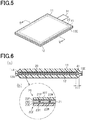
Fig. 5 is a perspective view illustrating the overall configuration of a light control device according to a modification. -
Fig. 6 is a cross-sectional view taken along line VI-VI ofFig. 5 . -
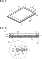
Fig. 7 is a perspective view illustrating the overall configuration of a light control device according to a modification. -
Fig. 8 is a cross-sectional view taken along line VIII-VIII ofFig. 7 . - A description will be given of an embodiment of a light control device and a method for producing the same.
- As shown in
Fig. 1 , the light control device has a rectangular sheet shape. The light control device is attached to a window provided to a moving body such as a vehicle or aircraft. The light control device can be also attached to a window of buildings, such as houses, stations, and airports, partitions in offices, and a display window in stores. Objects to which the light control device is attached may have various shapes such as flat, curved, and indefinite shapes. The light control device is attached to an object with an adhesive layer. The adhesive layer may be composed of any material as long as the layer is transparent and adhesive. An example of the adhesive layer is an OCA (Optical Clear Adhesive) film. The light control device can be made into a geometric shape other than a rectangle, a sheet shape such as an indefinite shape, or a plate shape. - The light control device includes a first
transparent coating substrate 11, a secondtransparent coating substrate 12, alight control sheet 20, apower supply wire 31, and a transparentadhesive layer 41. - The
transparent coating substrates transparent coating substrates light control sheet 20. Thetransparent coating substrates light control sheet 20 to each of thetransparent coating substrates transparent coating substrates - The
transparent coating substrates transparent coating substrates transparent coating substrates - The
transparent coating substrates light control sheet 20. The water absorption rate refers to a value in accordance with the method of JIS K 7209:2000 A. - The resin composing each of the
transparent coating substrates - To make the
light control sheet 20 more durable against ultraviolet light, thetransparent coating substrates transparent coating substrates - The
light control sheet 20 is located between the firsttransparent coating substrate 11 and the secondtransparent coating substrate 12. The entirelight control sheet 20 is covered by the firsttransparent coating substrate 11 as viewed perpendicular to the firsttransparent coating substrate 11. The entirelight control sheet 20 is covered by the secondtransparent coating substrate 12 as viewed perpendicular to the secondtransparent coating substrate 12. - The transparent
adhesive layer 41 is shaped like a rectangular frame as viewed perpendicular to the secondtransparent coating substrate 12. The transparentadhesive layer 41 is joined to a periphery of thefirst bonding surface 11A (seeFig. 2 ) of the firsttransparent coating substrate 11. The transparentadhesive layer 41 is joined to a periphery of thesecond bonding surface 12A (seeFig. 2 ) of the secondtransparent coating substrate 12. The transparentadhesive layer 41 is joined to an outer periphery (edge face) of thelight control sheet 20 and covers the entire edge face of thelight control sheet 20. - The
power supply wire 31 is separately connected to afirst electrode layer 22M (seeFig. 2 ) of thelight control sheet 20 and to asecond electrode layer 23M (seeFig. 2 ) of thelight control sheet 20. Thepower supply wire 31 includes separate conductive adhesive layers, such as anisotropic conductive films, joined to therespective electrode layers power supply wire 31 can be modified to include separate conductive paste layers joined to therespective electrode layers - The connection part between the
first electrode layer 22M and thepower supply wire 31 is covered by the firsttransparent coating substrate 11. The connection part between thesecond electrode layer 23M and thepower supply wire 31 is covered by the secondtransparent coating substrate 12. Thepower supply wire 31 is connected to a drive unit, which is located outside the light control device, and to thelight control sheet 20 through a part of the transparentadhesive layer 41. Thepower supply wire 31 applies a voltage for driving the light control device from a driving device between thefirst electrode layer 22M and thesecond electrode layer 23M. - As shown in
Fig. 2 , the firsttransparent coating substrate 11 includes afirst bonding surface 11A. The secondtransparent coating substrate 12 includes asecond bonding surface 12A. Thelight control sheet 20 is located between thefirst bonding surface 11A of the firsttransparent coating substrate 11 and thesecond bonding surface 12A of the secondtransparent coating substrate 12. Thefirst bonding surface 11A and thelight control sheet 20 are joined together with a transparent adhesive (first transparent adhesive). Thesecond bonding surface 12A and thelight control sheet 20 are joined together with a transparent adhesive (second transparent adhesive). - The transparent
adhesive layer 41 is joined to thefirst bonding surface 11A, thesecond bonding surface 12A, and asheet edge face 20E of the light control sheet 20 (see the partially enlarged view inFig. 2 ). The transparent adhesive that joins thefirst bonding surface 11A and thelight control sheet 20 together and the transparent adhesive that joins thesecond bonding surface 12A and thelight control sheet 20 together are joined to the transparentadhesive layer 41. The transparent adhesive that joins thefirst bonding surface 11A and thelight control sheet 20 together and the transparent adhesive that joins thesecond bonding surface 12A and thelight control sheet 20 together are integrated with the transparentadhesive layer 41. The main components of the transparent adhesive that joins thefirst bonding surface 11A and thelight control sheet 20 together and the transparent adhesive that joins thesecond bonding surface 12A and thelight control sheet 20 together are a type of resin identical to the main component of the transparent adhesive composing the transparentadhesive layer 41. Note that the main component refers to a component of a member having the highest formulation ratio among the components of the member. - The transparent adhesive that joins the
first bonding surface 11A and thelight control sheet 20 together and the transparent adhesive that joins thesecond bonding surface 12A and thelight control sheet 20 together may not be integrated with the transparentadhesive layer 41. The transparent adhesive that joins thefirst bonding surface 11A and thelight control sheet 20 together, the transparent adhesive that joins thesecond bonding surface 12A and thelight control sheet 20 together, and the transparent adhesive composing the transparentadhesive layer 41 can be resins of a type different from one another. If the main components of the transparent adhesive that joins thefirst bonding surface 11A and thelight control sheet 20 together, the transparent adhesive that joins thesecond bonding surface 12A and thelight control sheet 20 together, and the transparent adhesive composing the transparentadhesive layer 41 are an identical type of resin, then they can be adhered to each other more firmly. - The
light control sheet 20 includes afirst support film 22T, afirst electrode layer 22M, aliquid crystal layer 21, asecond support film 23T, and asecond electrode layer 23M. Thefirst support film 22T and thefirst electrode layer 22M constitute a first transparent electrode film. Thesecond support film 23T and thesecond electrode layer 23M constitute a second transparent electrode film. - The
first support film 22T is joined to thefirst bonding surface 11A via a transparent adhesive. Thefirst support film 22T supports thefirst electrode layer 22M on a side facing away from thefirst bonding surface 11A. Thesecond support film 23T is joined to thesecond bonding surface 12A via a transparent adhesive. Thesecond support film 23T supports thesecond electrode layer 23M on a side facing away from thesecond bonding surface 12A. - The
support films transparent coating substrates support films light control sheet 20. Thesupport films support films - The
support films support films support films - The electrode layers 22M and 23M each allow visible light to be transmitted therethrough and are electrically conductive. The electrode layers 22M and 23M are disposed over the entire side surfaces of the
support films - The electrode layers 22M and 23M are each composed of one type of material selected from the group consisting of indium tin oxide, fluorine-doped tin oxide, tin oxide, zinc oxide, carbon nanotubes, poly(3,4-ethylenedioxythiophene), and a silver alloy thin film.
- The
liquid crystal layer 21 is located between thefirst electrode layer 22M and thesecond electrode layer 23M. Theliquid crystal layer 21 fills the entire space between thefirst electrode layer 22M and thesecond electrode layer 23M. An edge face of theliquid crystal layer 21 is flush with an edge face of each of the electrode layers 22M and 23M and an edge face of each of thesupport films liquid crystal layer 21 preferably has a thickness of 10 µm or more to ensure that theliquid crystal layer 21 can be made more opaque. Theliquid crystal layer 21 preferably has a thickness of 100 µm or less to ensure that theliquid crystal layer 21 can be made more transparent. - The
liquid crystal layer 21 contains a liquid crystal composition. An example of liquid crystal molecules contained in the liquid crystal composition is one selected from the group consisting of those based on Schiff bases, azo types, azoxy types, biphenyls, terphenyls, benzoic acid esters, tolan types, pyrimidines, cyclohexanecarboxylic acid esters, phenylcyclohexanes, and dioxanes. Note that theliquid crystal layer 21 can contain a dye that has a predetermined color and has little influence on how the liquid crystal molecules move based on whether a voltage is applied to theliquid crystal layer 21. - The
liquid crystal layer 21 includes a polymer network that fills the entire space between thefirst electrode layer 22M and thesecond electrode layer 23M. The liquid crystal composition is held in voids in the polymer network. The type in which the liquid crystal composition is held is one selected from the group consisting of a polymer network type, a polymer dispersion type, and a capsule type. The polymer network type has a three-dimensional mesh polymer network, and holds a liquid crystal composition in voids in the polymer network. The polymer dispersion type has a large number of isolated voids in the polymer network and holds the liquid crystal composition in the voids dispersed in the polymer network. The capsule type holds an encapsulated liquid crystal composition in the polymer network. - The
liquid crystal layer 21 includesspacers 21P dispersed all over theliquid crystal layer 21. Thespacers 21P have a function of holding the thickness of theliquid crystal layer 21 constant. Thespacers 21P are each spherical having an average particle diameter that is substantially equal to the thickness of theliquid crystal layer 21. Thespacers 21P are each composed of either transparent inorganic material, such as silicon oxide, or transparent resin material, such as acrylic resin. Thespacer 21P preferably has a compressive fracture strength of 1 MPa or more to secure the thickness of theliquid crystal layer 21 when thetransparent coating substrates light control sheet 20 are joined together. - The
light control sheet 20 may have a functional layer other than theliquid crystal layer 21, the electrode layers 22M and 23M, and thesupport films - An example of the functional layer protects the
liquid crystal layer 21 and the electrode layers 22M and 23M, such as a gas barrier layer or an ultraviolet barrier layer. The gas barrier layer is located between thesupport films transparent coating substrates support films - An example of the functional layer contributes to the control of light transparency, such as an orientation layer or a polarizing layer. The orientation layer is located between each of the electrode layers 22M and 23M and the
liquid crystal layer 21. The polarizing layer is located between thesupport films transparent coating substrates support films - An example of the functional layer enhances the strength, heat resistance, etc. of the
light control sheet 20, such as a hard coat layer. The hard coat layer is located between thesupport films transparent coating substrates light control sheet 20. - The type of the
light control sheet 20 is either a normal type or a reverse type. The normal type achieves high transmittance by voltage application between thefirst electrode layer 22M and thesecond electrode layer 23M. The normal type achieves low transmittance by suspension of voltage application between thefirst electrode layer 22M and thesecond electrode layer 23M. In contrast, the reverse type achieves low transmittance by voltage application between thefirst electrode layer 22M and thesecond electrode layer 23M. The reverse type achieves high transmittance by suspension of voltage application between thefirst electrode layer 22M and thesecond electrode layer 23M. - An edge face of the first
transparent coating substrate 11, an edge face of the secondtransparent coating substrate 12, and an edge face (outer side) of the transparentadhesive layer 41 constitute an edge face of the light control device. The edge face of the light control device is exposed outside the light control device. The edge face of the light control device has a cutting mark. The cutting mark on the edge face of the light control device is a mark that is made when the light control device is cut in a thickness direction thereof with the firsttransparent coating substrate 11, the secondtransparent coating substrate 12, and the transparentadhesive layer 41 being as a single unit. An example of the cutting mark extends from the edge face of the firsttransparent coating substrate 11 to the outer side of the transparentadhesive layer 41. An example of the cutting mark extends from the edge face of the secondtransparent coating substrate 12 to the outer side of the transparentadhesive layer 41. An example of the cutting mark on the transparentadhesive layer 41 has a line extending in a circumferential direction of the light control device, in a thickness direction of the light control device, or in a direction intersecting with these directions. - The edge face of the light control device is inclined relative to a normal direction of the
first bonding surface 11A and to a normal direction of thesecond bonding surface 12A. The outer side of the transparentadhesive layer 41 may intersect the normal direction of thefirst bonding surface 11A or the normal direction of thesecond bonding surface 12A. In the example shown inFig. 2 , the edge face of the light control device is curved, being convex in a direction in which thelight control sheet 20 extends. The edge face of the light control device constitutes a hypotenuse of a trapezoid in cross-sectional view of the light control device. - Since the outer side of the transparent
adhesive layer 41 has the cutting mark, the thickness thereof can be adjusted by cutting. For example, a transparent adhesive is cured as an edge face of the light control device, and part of the cured material is cut, thereby forming the transparentadhesive layer 41. - The sheet edge face 20E, which serves as an edge face of the
light control sheet 20, includes an edge face of each of thesupport films edge face 21E of theliquid crystal layer 21. The transparentadhesive layer 41 is a cured transparent adhesive that covers the entiresheet edge face 20E. The transparentadhesive layer 41 has a water absorption rate of 2% or less. The water absorption rate of the transparentadhesive layer 41 refers to a value in accordance with the method of JIS K 7209:2000 A. To enhance the waterproofness relative to thelight control sheet 20, the firsttransparent coating substrate 11 and the secondtransparent coating substrate 12 are preferably joined together by the transparentadhesive layer 41 so as to cover the transparentadhesive layer 41. - The
thickness 41T of the transparentadhesive layer 41 in the direction in which thelight control sheet 20 extends is preferably 1 mm or more to enhance the waterproofness relative to thelight control sheet 20. Theminimum thickness 41T of the transparentadhesive layer 41 is preferably 1 mm or more if thethickness 41T thereof is not constant in the thickness direction of the transparentadhesive layer 41. - The
thickness 41T of the transparentadhesive layer 41 is preferably 5 mm or less to ensure that the transparentadhesive layer 41 can have better designability as viewed perpendicular to thelight control sheet 20. Themaximum thickness 41T of the transparentadhesive layer 41 is preferably 5 mm or less if thethickness 41T thereof is not constant in the thickness direction of the transparentadhesive layer 41. In the example shown inFig. 2 , for example, preferably, the part of the transparentadhesive layer 41 having theminimum thickness 41T is in contact with the firsttransparent coating substrate 11 and has a thickness of 1 mm or more. Preferably, the part of the transparentadhesive layer 41 having themaximum thickness 41T is in contact with the firsttransparent coating substrate 11 and has a thickness of 5 mm or less. - The main component of the transparent adhesive composing the transparent
adhesive layer 41 is one selected from the group consisting of polypropylene, polyurethane, acrylic resins such as a polymethyl methacrylate or styrene-methacrylic acid copolymer, polystyrene-based resins such as polystyrene or a styrene acrylonitrile copolymer or an acrylonitrile-butadienestyrene copolymer, silicone-based resin, and epoxy-based resin. - Preferably, the main component of the transparent adhesive composing the transparent
adhesive layer 41 is an acrylic resin so as to achieve a low molding temperature. The transparent adhesive constituting the transparentadhesive layer 41 is preferably an acrylic resin for its high bending strength and tensile strength in constituting an edge portion of the light control device. - Polypropylene has a water absorption rate of less than 0.01%. Polyurethane has a water absorption rate of less than 0.01%. The acrylic resin has a water absorption rate of 0.2% or more and 0.4% or less. The polystyrene-based resin has a water absorption rate of less than 0.1%. The silicone-based resin has a water absorption rate of 1%. The epoxy resin has a water absorption rate of 2% or less. Cellulose acetate and polyvinyl alcohol cannot be used as the transparent adhesive composing the transparent
adhesive layer 41 because cellulose acetate has a water absorption rate of 1.9% or more and 6.5% or less and polyvinyl alcohol has a water absorption rate of 30% or more. - Preferably, the main component of the transparent adhesive composing the transparent
adhesive layer 41 is a type of resin identical to the main component of the firsttransparent coating substrate 11 and the main component of the second transparent coating substrate. If these main components are all an identical type of resin, the transparentadhesive layer 41, the firsttransparent coating substrate 11, and the second transparent coating substrate can be adhered to each other more firmly. - In the configuration where the transparent
adhesive layer 41 joins the firsttransparent coating substrate 11 and the secondtransparent coating substrate 12, thetransparent coating substrates light control sheet 20 is pressed by the firsttransparent coating substrate 11 and the secondtransparent coating substrate 12. Thetransparent coating substrates adhesive layer 41, exert an external force on thelight control sheet 20 so that theliquid crystal layer 21 is sandwiched by thefirst electrode layer 22M and thesecond electrode layer 23M. This can prevent the layers constituting thelight control sheet 20 from separating from each other. In addition, theliquid crystal layer 21 having a polymer network andspacers 21P can prevent a distance between the electrode layers 22M and 23M from varying due to the action of the external force described above. - A method for producing the light control device involves laminating the first
transparent coating substrate 11, the secondtransparent coating substrate 12, and thelight control sheet 20 so that thelight control sheet 20 is sandwiched by the firsttransparent coating substrate 11 and the secondtransparent coating substrate 12. The lamination method is a dry lamination method in which a transparent adhesive is heated and pressed to cure it. - As shown in
Fig. 3 , anuncured adhesive layer 41P, the main component of which is a thermosetting transparent adhesive, is initially formed on thefirst bonding surface 11A of the firsttransparent coating substrate 11, and then thelight control sheet 20 is attached to theuncured adhesive layer 41P. At this time, thelight control sheet 20 is attached to theuncured adhesive layer 41P so that thesheet edge face 20E of thelight control sheet 20 is mostly covered by theuncured adhesive layer 41P. For example, thelight control sheet 20 attached to theuncured adhesive layer 41P exposes only an edge face of asecond support film 23T from theuncured adhesive layer 41P. - The
light control sheet 20 is cut out of a large sheet with has each of the layers constituting thelight control sheet 20, into a desired shape. Thesheet edge face 20E of thelight control sheet 20 is formed by cutting out from a multilayered sheet. Thepower supply wire 31 is separately joined to each of the electrode layers 22M and 23M of thelight control sheet 20. - The dry lamination method involves first applying an adhesive solution containing a thermosetting transparent adhesive to the
first bonding surface 11A of the firsttransparent coating substrate 11 in formation of theuncured adhesive layer 41P. The adhesive solution is applied onto thefirst bonding surface 11A with a doctor blade. The film produced by the application of the adhesive solution is dried in a drying device to form theuncured adhesive layer 41P, the main component of which is the transparent adhesive. - The
first bonding surface 11A of the firsttransparent coating substrate 11 may be coated in advance with an adhesion aid to adhere theuncured adhesive layer 41P and thefirst bonding surface 11A more firmly in advance of the formation of theuncured adhesive layer 41P. - As shown in
Fig. 4 , anuncured adhesive layer 41P, the main component of which is a thermosetting transparent adhesive, is then formed on thesecond bonding surface 12A of the secondtransparent coating substrate 12, and thelight control sheet 20 attached to the firsttransparent coating substrate 11 is attached thereto together with the firsttransparent coating substrate 11. At this time, theuncured adhesive layer 41P on thefirst bonding surface 11A and theuncured adhesive layer 41P on thesecond bonding surface 12A are joined together so that the entiresheet edge face 20E of thelight control sheet 20 is covered by the uncuredadhesive layers 41P. The mutually joined uncuredadhesive layers 41P form the transparentadhesive layer 41 by curing the uncuredadhesive layers 41P and cutting part of the cured material. - Note that in cases where a thermoplastic transparent adhesive is used, a layer composed of a cured transparent adhesive is used instead of the
uncured adhesive layer 41P. Then, with the firsttransparent coating substrate 11 positioned relative to thelight control sheet 20, while the firsttransparent coating substrate 11 is being heated, the layer composed of a softened transparent adhesive is pressed against thelight control sheet 20 The pressed firsttransparent coating substrate 11 is cooled, thereby curing the layer composed of the transparent adhesive. In addition, with the secondtransparent coating substrate 12 positioned relative to thelight control sheet 20, while the secondtransparent coating substrate 12 is being heated, the layer composed of a softened transparent adhesive is pressed against thelight control sheet 20 The pressed secondtransparent coating substrate 12 is cooled, thereby curing the layer composed of the transparent adhesive so that the entire sheet edge face 20E is covered by the transparent adhesive. - Part of the cured material is cut approximately along a thickness direction of a light control device with the first
transparent coating substrate 11, the secondtransparent coating substrate 12, and the cured material being as a single unit, as indicated by the arrows inFig. 4 . By cutting part of the cured material, thethickness 41T of the transparentadhesive layer 41 is adjusted to, for example, 1 mm or more and 5 mm or less. The cutting is performed such that as a blade for cutting the cured material approaches from the firsttransparent coating substrate 11 to the secondtransparent coating substrate 12, the blade moves outward in a direction in which thelight control sheet 20 extends. Thus, the edge faces of the light control device each constitute a hypotenuse of a trapezoid in cross-sectional view of the light control device, as shown inFig. 2 . - At this time, the first
transparent coating substrate 11 and the secondtransparent coating substrate 12 are pressed against each other to be joined together. The pressing force that brings thetransparent coating substrates transparent coating substrates transparent coating substrates transparent coating substrates transparent coating substrates transparent coating substrates transparent coating substrates - The pressing force described above also acts on the
light control sheet 20 located between the firsttransparent coating substrate 11 and the secondtransparent coating substrate 12. A change in the distance between thefirst electrode layer 22M and thesecond electrode layer 23M changes a capacitance and other electrical properties of theliquid crystal layer 21. Particularly in theliquid crystal layer 21, where a polymer network is formed between thefirst electrode layer 22M and thesecond electrode layer 23M, the distance between thefirst electrode layer 22M and thesecond electrode layer 23M is determined by formation of theliquid crystal layer 21. If the pressing force described above additionally acts on thelight control sheet 20, the distance therebetween readily changes. - A compressive fracture strength of 1 MPa or more of the
spacers 21P is sufficiently higher than the pressing force applied to thetransparent coating substrates liquid crystal layer 21 can maintain its thickness at an average particle diameter of thespacers 21P even if the pressing force described above is applied in the process of producing the light control device. - A normal type
light control sheet 20 was prepared with thesupport films liquid crystal layer 21 being configured as listed below. The light control device in a test example was then prepared using a dry lamination method with thetransparent coating substrates adhesive layer 41 being configured as listed below. -
Support films - Support film thickness: 50 µm
- Electrode layers 22M and 23M: Indium tin oxide
- Thickness of
electrode layers - Thickness of liquid crystal layer 21: 20 µm
-
Transparent coating substrates 11 and 12: Acrylic resin films - Thickness of transparent coating substrate: 100 µm
-
Spacer 21P: Acrylic resin particles - Average particle diameter of
spacer 21P: 20 µm - Transparent adhesive layer 41: Acrylic resin
- A water immersion test was conducted in accordance with JIS C 0920 2003 (IPX7) with the light control device of the test example to check its operation with and without application of a driving voltage, to conduct visual observation for water penetration into the light control device, and to measure a haze value of the light control device before and after the test in a state in which a driving voltage is applied (in the transparent state). After the test, the light control device of the test example was observed to operate in the same manner as before the test, to allow no water penetration under visual observation, and to increase in haze value by less than 2%.
- Similar results were obtained when the transparent
adhesive layer 41 was composed of polypropylene, polyurethane, polystyrene resin, silicone-based resin, and epoxy resin. When the transparentadhesive layer 41 was composed of cellulose acetate or polyvinyl alcohol, on the other hand, visual observation after the test found water penetration from the sheet edge face 20E into thelight control sheet 20 and presence of an area that was made transparent and an area that was insensitive to application of driving voltage at an edge portion of theliquid crystal layer 21. - According to the present embodiment, the advantageous effects listed below can be achieved.
- (1) The
light control sheet 20 is located between the firsttransparent coating substrate 11 and the secondtransparent coating substrate 12, which enhances the waterproofness relative to theliquid crystal layer 21 on afirst electrode layer 22M side relative to theliquid crystal layer 21 and on asecond electrode layer 23M side relative thereto. In addition, the transparentadhesive layer 41, which enhances the waterproofness, is transparent, thus preventing deterioration in designability when the transparentadhesive layer 41 is visually recognized. - (2) In addition, the
sheet edge face 20E including an edge face of theliquid crystal layer 21 is covered by the transparentadhesive layer 41 whose water absorption rate is 2% or less, which enhances the waterproofness relative to the edge face of theliquid crystal layer 21. - (3) The
transparent coating substrates light control sheet 20 so that theliquid crystal layer 21 is sandwiched by thefirst electrode layer 22M and thesecond electrode layer 23M. This can prevent the layers constituting thelight control sheet 20 from separating from each other. - (4) In addition, the
liquid crystal layer 21 having a polymer network andspacers 21P can prevent a distance between the electrode layers 22M and 23M from varying due to an action of the external force. - (5) A compressive fracture strength of 1 MPa or more of the
spacers 21P makes it possible to readily employ the method for pressing thelight control sheet 20 between thetransparent coating substrates - (6) A
thickness 41T of 1 mm or more of the transparentadhesive layer 41 enhances the waterproofness relative to theliquid crystal layer 21. Athickness 41T of 5 mm or less of the transparentadhesive layer 41 makes it possible to maintain the designability of the light control unit. - (7) If the outer side of the transparent
adhesive layer 41 has a cutting mark, cutting the transparentadhesive layer 41 can adjust the thickness and shape thereof. - (8) If the main components of the
transparent coating substrates adhesive layer 41 are an identical type of resin, they can be joined more firmly. - (9) If the main component of each transparent adhesive is an identical type of resin, this enhances the waterproofness relative to each part covered by the cured material of the transparent adhesive. In addition, the same transparent adhesive may be used as the respective transparent adhesives, which simplifies the light control device and the production method thereof.
- (10) If the connection parts between the electrode layers 22M and 23M and the
power supply wire 31 are covered by thetransparent coating substrates - (11) If the main components of the transparent adhesive for joining the
support films adhesive layer 41 are an identical type of resin, the same transparent adhesive may be used as the respective transparent adhesives. This in turn simplifies the light control unit and the production method thereof. - The above embodiment may be implemented with modifications as described below:
- As shown in
Fig. 5 , the transparentadhesive layer 41 may be located around thelight control sheet 20, and an edge portion of the firsttransparent coating substrate 11 and an edge portion of the secondtransparent coating substrate 12 may be joined together so as to cover the transparentadhesive layer 41. In other words, the transparentadhesive layer 41 joins the sheet edge face 20E and the bonding surfaces 11A and 12A around thelight control sheet 20, as shown inFig. 6 . The edge portion of the firsttransparent coating substrate 11 and the edge portion of the secondtransparent coating substrate 12 are joined together outside the transparentadhesive layer 41 so as to cover an edge face of the transparentadhesive layer 41. - The method for producing the light control device in this modification involves laminating the first
transparent coating substrate 11, the secondtransparent coating substrate 12, and thelight control sheet 20 so that thelight control sheet 20 is sandwiched by the firsttransparent coating substrate 11 and the secondtransparent coating substrate 12, as with the embodiment described above. On the other hand, theuncured adhesive layer 41P formed on thefirst bonding surface 11A of the firsttransparent coating substrate 11 and theuncured adhesive layer 41P formed on thesecond bonding surface 12A of the secondtransparent coating substrate 12 are sufficiently thinner on the edge portion of the firsttransparent coating substrate 11 and on the edge portion of the secondtransparent coating substrate 12 than in other places. Joining thetransparent coating substrates - (12) This modification enables a
joint portion 10E between the firsttransparent coating substrate 11 and the secondtransparent coating substrate 12 to further enhance the waterproofness relative to the edge face of theliquid crystal layer 21. - (13) The joining of the
transparent coating substrates - As shown in
Fig. 7 , the firsttransparent coating substrate 11 may have an opposite surface facing away from thefirst bonding surface 11A and may further have anopening 11K that extends between thefirst bonding surface 11A and the opposite surface. Theopening 11K is rectangular as viewed perpendicular to the firsttransparent coating substrate 11. As shown inFig. 8 , theopening 11K extends from the opposite surface of the firsttransparent coating substrate 11 through a surface of thelight control sheet 20. Theopening 11K faces an area of thelight control sheet 20 surrounded by thesheet edge face 20E.
The method for producing the light control device in this modification involves laminating the firsttransparent coating substrate 11, the secondtransparent coating substrate 12, and thelight control sheet 20 so that thelight control sheet 20 is sandwiched by the firsttransparent coating substrate 11 and the secondtransparent coating substrate 12, as with the embodiment described above. A part of the firsttransparent coating substrate 11 and the transparent adhesive that joins thefirst bonding surface 11A and thelight control sheet 20 are then cut so as to provide a border of theopening 11K. - As shown in
- (14) This modification exposes a part of the
light control sheet 20 from the firsttransparent coating substrate 11, which can prevent deterioration in light transmittance caused by the transparent adhesive located between the firsttransparent coating substrate 11 and thelight control sheet 20, and the firsttransparent coating substrate 11.- The light control device may have a different configuration in which the
power supply wire 31 is omitted and the entire periphery of thelight control sheet 20 is covered by the transparentadhesive layer 41. In this case, the electrode layers 22M and 23M and thepower supply wire 31 are connected together by removing part of thetransparent coating substrates
- The light control device may have a different configuration in which the
-
- 11: First transparent coating substrate
- 11A: First bonding surface
- 11K: Opening
- 12: Second transparent coating substrate
- 12A: Second bonding surface
- 20: Light control sheet
- 20E: Sheet edge face
- 21: Liquid crystal layer
- 21P: Spacer
- 22E, 23E: Edge face
- 22M: First electrode layer
- 22T: First support film
- 23M: Second electrode layer
- 23T: Second support film
- 31: Power supply wire
- 41: Transparent adhesive layer
- 41P: Uncured adhesive layer
Claims (11)
- A light control device comprising:a first transparent coating substrate having a first bonding surface;a second transparent coating substrate having a second bonding surface;a light control sheet located between the first bonding surface and second bonding surface, wherein: the light control sheet includes:a first transparent electrode film including a first electrode layer and a first support film that supports the first electrode layer, the first support film being joined to the first bonding surface via a first transparent adhesive;a second transparent electrode film including a second electrode layer and a second support film that supports the second electrode layer, the second support film being joined to the second bonding surface via a second transparent adhesive; anda liquid crystal layer including a liquid crystal composition that fills space between the first transparent electrode film and the second transparent electrode film; and wherein an edge face of the first electrode layer, an edge face of the second electrode layer, and an edge face of the liquid crystal layer constitute a sheet edge face; anda transparent adhesive layer that covers the sheet edge face and joins the first bonding surface and the second bonding surface together around the light control sheet, the transparent adhesive layer having a water absorption rate of 2% or less in accordance with a method of JIS K 7209:2000 A.
- The light control device according to claim 1, wherein the transparent adhesive layer has a thickness of 1 mm or more and 5 mm or less in a direction in which the light control sheet extends.
- The light control device according to claim 1 or 2, wherein
the liquid crystal layer has spacers dispersed in the liquid crystal layer; and
the spacers have a compressive fracture strength of IMPa or more. - The light control device according to any one of claims 1 to 3, wherein
the transparent adhesive layer is located around the light control sheet; and
an edge portion of the first transparent coating substrate and an edge portion of the second transparent coating substrate are joined together so as to cover the transparent adhesive layer on a side opposite to the light control sheet. - The light control device according to any one of claims 1 to 3, wherein the transparent adhesive layer comprises an inner side facing the sheet edge face and an outer side exposed to an outside of the light control device in a direction in which the light control sheet extends, and the outer side comprises a cutting mark contiguous to an edge face of each transparent coating substrate.
- The light control device according to any one of claims 1 to 5, wherein main components of the first transparent coating substrate, the second transparent coating substrate, and the transparent adhesive layer are an identical type of resin.
- The light control device according to any one of claims 1 to 6, wherein main components of the first transparent adhesive, the second transparent adhesive, and a transparent adhesive composing the transparent adhesive layer are an identical type of resin.
- The light control device according to any one of claims 1 to 7, wherein the first transparent coating substrate comprises an opposite surface facing away from the first bonding surface and further has an opening that extends between the first bonding surface and the opposite surface, the opening facing an area of the light control sheet surrounded by the sheet edge face.
- The light control device according to any one of claims 1 to 8, further comprising a power supply wire connected to the first electrode layer, wherein a part at which the first electrode layer and the power supply wire are connected to each other is covered by the first transparent coating substrate via the first transparent adhesive.
- A method for producing a light control device, comprising:preparing a light control sheet comprising a liquid crystal layer that includes a liquid crystal composition filling voids in a polymer network and that includes spacers dispersed in the liquid crystal layer, the liquid crystal layer being located between a first electrode layer supported by a first support film and a second electrode layer supported by a second support film, where an edge face of the first electrode layer, an edge face of the second electrode layer, and an edge face of the liquid crystal layer constitute a sheet edge face;laminating a first transparent coating substrate, a second transparent coating substrate, and the light control sheet so that the light control sheet is sandwiched by the first transparent coating substrate and the second transparent coating substrate; andcovering the sheet edge face with a transparent adhesive layer and joining a first bonding surface and a second bonding surface with the transparent adhesive layer around the light control sheet, the transparent adhesive layer having a water absorption rate of 2% or less in accordance with a method of JIS K 7209:2000 A.
- The method for producing a light control device according to claim 10, wherein
the laminating includes joining the first support film to the first transparent coating substrate via a first transparent adhesive and joining the second support film to the second transparent coating substrate via a second transparent adhesive; and
the covering the sheet edge face includes forming the transparent adhesive layer by covering the sheet edge face with the first and second transparent adhesives and curing the first and second transparent adhesives.
Applications Claiming Priority (2)
| Application Number | Priority Date | Filing Date | Title |
|---|---|---|---|
| JP2018158481A JP6669214B2 (en) | 2018-08-27 | 2018-08-27 | Light control device and method for manufacturing light control device |
| PCT/JP2019/033434 WO2020045389A1 (en) | 2018-08-27 | 2019-08-27 | Light control device and method for producing light control device |
Publications (2)
| Publication Number | Publication Date |
|---|---|
| EP3845957A1 true EP3845957A1 (en) | 2021-07-07 |
| EP3845957A4 EP3845957A4 (en) | 2021-10-13 |
Family
ID=69645197
Family Applications (1)
| Application Number | Title | Priority Date | Filing Date |
|---|---|---|---|
| EP19855617.7A Withdrawn EP3845957A4 (en) | 2018-08-27 | 2019-08-27 | Light control device and method for producing light control device |
Country Status (5)
| Country | Link |
|---|---|
| US (1) | US11448924B2 (en) |
| EP (1) | EP3845957A4 (en) |
| JP (1) | JP6669214B2 (en) |
| CN (1) | CN112368632A (en) |
| WO (1) | WO2020045389A1 (en) |
Families Citing this family (7)
| Publication number | Priority date | Publication date | Assignee | Title |
|---|---|---|---|---|
| JP7467993B2 (en) * | 2020-03-06 | 2024-04-16 | Toppanホールディングス株式会社 | Light-adjusting sheet and light-adjusting device |
| WO2022039089A1 (en) | 2020-08-21 | 2022-02-24 | Agc株式会社 | Laminated glass, and method for manufacturing laminated glass |
| JP7539039B2 (en) * | 2021-01-15 | 2024-08-23 | 大日本印刷株式会社 | Light control device and manufacturing method thereof |
| JP7558104B2 (en) | 2021-03-31 | 2024-09-30 | 株式会社ジャパンディスプレイ | Optical Elements |
| CN114002867B (en) * | 2021-10-08 | 2022-11-29 | 北京大学 | Trans-mode light adjusting film based on liquid crystal epoxy photoinitiated ring-opening polymerization and preparation method thereof |
| JP2024012996A (en) * | 2022-07-19 | 2024-01-31 | Toppanホールディングス株式会社 | Light control sheet and method for manufacturing light control sheet |
| CN119278405B (en) * | 2022-12-27 | 2026-02-17 | 京东方科技集团股份有限公司 | Dimming device, preparation method thereof and vehicle |
Family Cites Families (31)
| Publication number | Priority date | Publication date | Assignee | Title |
|---|---|---|---|---|
| JPH01186911A (en) * | 1988-01-21 | 1989-07-26 | Asahi Glass Co Ltd | Dimming device and its manufacture |
| JP2712327B2 (en) | 1988-07-14 | 1998-02-10 | 旭硝子株式会社 | REINFORCED LIQUID CRYSTAL OPTICAL ELEMENT, ITS MANUFACTURING METHOD, AND LIGHT CONTROL DEVICE |
| JPH0571822U (en) * | 1992-02-28 | 1993-09-28 | タキロン株式会社 | Light control panel |
| US7838115B2 (en) * | 1995-04-11 | 2010-11-23 | Magna Mirrors Of America, Inc. | Method for manufacturing an articulatable vehicular window assembly |
| JP2001215484A (en) * | 2000-02-03 | 2001-08-10 | Kawaguchiko Seimitsu Co Ltd | Liquid crystal ink for printing and liquid crystal display device using the same |
| US6646205B2 (en) * | 2000-12-12 | 2003-11-11 | Sumitomo Wiring Systems, Ltd. | Electrical wire having a resin composition covering |
| TW200506469A (en) * | 2003-06-13 | 2005-02-16 | Sekisui Chemical Co Ltd | Method for manufacturing liquid crystal display |
| JP2005017860A (en) * | 2003-06-27 | 2005-01-20 | Asahi Glass Co Ltd | Manufacturing method of liquid crystal light control device |
| US7688497B2 (en) * | 2007-01-22 | 2010-03-30 | E Ink Corporation | Multi-layer sheet for use in electro-optic displays |
| CN101900908B (en) * | 2009-05-27 | 2012-01-25 | 比亚迪股份有限公司 | Energy-saving dimming glass |
| TW201110802A (en) * | 2009-06-24 | 2011-03-16 | Seiko Epson Corp | Electro-optical device, electronic device, and illumination apparatus |
| JP5443941B2 (en) * | 2009-10-23 | 2014-03-19 | 積水化学工業株式会社 | Sealant for liquid crystal dropping method, vertical conduction material, and liquid crystal display element |
| JP2013161023A (en) * | 2012-02-08 | 2013-08-19 | Sony Corp | Display device and electronic apparatus |
| FR2997770B1 (en) * | 2012-11-07 | 2015-11-20 | Saint Gobain | ELECTROCONDUCTIVE SUPPORT FOR VARIABLE DIFFUSION GLAZING BY LIQUID CRYSTALS, AND SUCH A GLAZING |
| CN103064209B (en) * | 2013-01-30 | 2015-09-30 | 京东方科技集团股份有限公司 | A kind of display panels preparation method |
| JP6155062B2 (en) * | 2013-03-19 | 2017-06-28 | 本田技研工業株式会社 | Light control panel structure and manufacturing method thereof |
| WO2014171470A1 (en) * | 2013-04-19 | 2014-10-23 | 本田技研工業株式会社 | Light-adjusting-panel structure |
| US8994042B2 (en) * | 2013-05-20 | 2015-03-31 | Lg Electronics Inc. | Display panel and display device |
| CN103278976B (en) * | 2013-05-30 | 2016-01-20 | 京东方科技集团股份有限公司 | Liquid crystal panel and preparation method thereof, display device |
| CN103412429B (en) * | 2013-07-26 | 2016-12-28 | 京东方科技集团股份有限公司 | A kind of preparation method of display panels |
| CN104914629B (en) * | 2014-03-14 | 2019-03-01 | 群创光电股份有限公司 | Display device |
| CN105275334A (en) * | 2014-06-25 | 2016-01-27 | 南京晶多新材料科技有限公司 | Structure and application of strain light modulation window |
| KR102303244B1 (en) * | 2015-04-15 | 2021-09-17 | 삼성디스플레이 주식회사 | Display apparatus and method for manufacturing the same |
| EP3388403B1 (en) * | 2015-12-09 | 2020-12-02 | AGC Inc. | Laminated glass |
| JP6643944B2 (en) * | 2016-04-25 | 2020-02-12 | 日本化薬株式会社 | Sealant for liquid crystal optical element and liquid crystal optical element using the same |
| CN105892135A (en) * | 2016-06-27 | 2016-08-24 | 京东方科技集团股份有限公司 | Mother board panel, display panel, display device and manufacturing method for display panel |
| WO2018038743A1 (en) * | 2016-08-26 | 2018-03-01 | Jiansheng Wang | Laminated switchable panel and methods for making and using |
| JP2018040883A (en) | 2016-09-06 | 2018-03-15 | 北川工業株式会社 | Dimmer device |
| CN107885005B (en) * | 2016-09-30 | 2021-04-30 | 元太科技工业股份有限公司 | Waterproof display device |
| CN106997116B (en) * | 2017-04-28 | 2018-02-23 | 深圳市唯酷光电有限公司 | The preparation method and preparation facilities of the hand-written film of liquid crystal, the hand-written film of liquid crystal |
| WO2018223902A1 (en) * | 2017-06-06 | 2018-12-13 | The Hong Kong University Of Science And Technology | Haze free reverse mode liquid crystal light control film with inhomogeneous alignment layer |
-
2018
- 2018-08-27 JP JP2018158481A patent/JP6669214B2/en not_active Ceased
-
2019
- 2019-08-27 EP EP19855617.7A patent/EP3845957A4/en not_active Withdrawn
- 2019-08-27 WO PCT/JP2019/033434 patent/WO2020045389A1/en not_active Ceased
- 2019-08-27 CN CN201980045426.XA patent/CN112368632A/en active Pending
-
2021
- 2021-03-01 US US17/188,241 patent/US11448924B2/en active Active
Also Published As
| Publication number | Publication date |
|---|---|
| CN112368632A (en) | 2021-02-12 |
| JP2020034612A (en) | 2020-03-05 |
| US20210208439A1 (en) | 2021-07-08 |
| EP3845957A4 (en) | 2021-10-13 |
| US11448924B2 (en) | 2022-09-20 |
| JP6669214B2 (en) | 2020-03-18 |
| WO2020045389A1 (en) | 2020-03-05 |
Similar Documents
| Publication | Publication Date | Title |
|---|---|---|
| US11448924B2 (en) | Light control device comprising a transparent adhesive layer covering a sheet edge face of a light control sheet and method for producing the same | |
| JP4943860B2 (en) | Process for sealing electro-optic displays | |
| TWI444942B (en) | Bezelless display system and method for construction thereof | |
| US20230202147A1 (en) | Light modulating device and manufacturing method | |
| TWI741970B (en) | Method for producing a flexible electro-optic cell enclosed by a border seal and filled with an electro-optic material and flexible electro-optic cell enclosed by a border seal | |
| CN103733124A (en) | Polarizer device with adhesive layer | |
| WO2022138762A1 (en) | Dimmer device, method for manufacturing same, and liquid crystal device | |
| JP7377422B2 (en) | Light control device, light control window, and manufacturing method of light control device | |
| EP4249996A1 (en) | Light control sheet and method for manufacturing light control sheet | |
| TW201215982A (en) | Electrophoretic display structure | |
| JP2021124677A (en) | Dimming cell and dimming device | |
| TW202346994A (en) | Electro-optic display stacks with segmented electrodes and methods of making the same | |
| WO2020235580A1 (en) | Dimmer sheet and dimmer device | |
| KR20240090364A (en) | Multi-curved optical device and method for forming the same | |
| JP7409125B2 (en) | Light control device and its manufacturing method | |
| JP2022109495A (en) | Dimming device and manufacturing method thereof | |
| US20250010587A1 (en) | Laminated glass and liquid crystal device | |
| JP2022164932A (en) | Light control cell, light control device, vehicle, method for manufacturing light control cell, and method for manufacturing light control device | |
| CN221759745U (en) | Packaging film and display substrate | |
| JP7861815B2 (en) | Dimming sheet and dimming device | |
| JP2023028885A (en) | Manufacturing method for liquid crystal device | |
| WO2025005207A1 (en) | Light control member and laminated plate | |
| JP2026020991A (en) | Light control device and method for manufacturing the same | |
| WO2023127932A1 (en) | Light control laminate and light control device | |
| JP2025161570A (en) | Light control components and laminated plates |
Legal Events
| Date | Code | Title | Description |
|---|---|---|---|
| STAA | Information on the status of an ep patent application or granted ep patent |
Free format text: STATUS: THE INTERNATIONAL PUBLICATION HAS BEEN MADE |
|
| STAA | Information on the status of an ep patent application or granted ep patent |
Free format text: STATUS: REQUEST FOR EXAMINATION WAS MADE |
|
| PUAI | Public reference made under article 153(3) epc to a published international application that has entered the european phase |
Free format text: ORIGINAL CODE: 0009012 |
|
| 17P | Request for examination filed |
Effective date: 20201222 |
|
| AK | Designated contracting states |
Kind code of ref document: A1 Designated state(s): AL AT BE BG CH CY CZ DE DK EE ES FI FR GB GR HR HU IE IS IT LI LT LU LV MC MK MT NL NO PL PT RO RS SE SI SK SM TR |
|
| A4 | Supplementary search report drawn up and despatched |
Effective date: 20210914 |
|
| RIC1 | Information provided on ipc code assigned before grant |
Ipc: B32B 27/08 20060101ALI20210908BHEP Ipc: G02F 1/1334 20060101ALI20210908BHEP Ipc: B32B 17/10 20060101AFI20210908BHEP |
|
| DAV | Request for validation of the european patent (deleted) | ||
| DAX | Request for extension of the european patent (deleted) | ||
| REG | Reference to a national code |
Ref country code: DE Ref legal event code: R079 Free format text: PREVIOUS MAIN CLASS: G02F0001130000 Ipc: B32B0017100000 |
|
| GRAP | Despatch of communication of intention to grant a patent |
Free format text: ORIGINAL CODE: EPIDOSNIGR1 |
|
| STAA | Information on the status of an ep patent application or granted ep patent |
Free format text: STATUS: GRANT OF PATENT IS INTENDED |
|
| RIC1 | Information provided on ipc code assigned before grant |
Ipc: B32B 27/08 20060101ALI20230210BHEP Ipc: G02F 1/1334 20060101ALI20230210BHEP Ipc: B32B 17/10 20060101AFI20230210BHEP |
|
| INTG | Intention to grant announced |
Effective date: 20230322 |
|
| P01 | Opt-out of the competence of the unified patent court (upc) registered |
Effective date: 20230530 |
|
| STAA | Information on the status of an ep patent application or granted ep patent |
Free format text: STATUS: THE APPLICATION IS DEEMED TO BE WITHDRAWN |
|
| 18D | Application deemed to be withdrawn |
Effective date: 20230802 |