EP3845893A1 - Device and method applicable for measuring thickness of ultrathin film on substrate - Google Patents
Device and method applicable for measuring thickness of ultrathin film on substrate Download PDFInfo
- Publication number
- EP3845893A1 EP3845893A1 EP20171530.7A EP20171530A EP3845893A1 EP 3845893 A1 EP3845893 A1 EP 3845893A1 EP 20171530 A EP20171530 A EP 20171530A EP 3845893 A1 EP3845893 A1 EP 3845893A1
- Authority
- EP
- European Patent Office
- Prior art keywords
- fluorescence
- ray
- substrate
- ultrathin film
- thickness
- Prior art date
- Legal status (The legal status is an assumption and is not a legal conclusion. Google has not performed a legal analysis and makes no representation as to the accuracy of the status listed.)
- Granted
Links
Images



Classifications
-
- G—PHYSICS
- G01—MEASURING; TESTING
- G01B—MEASURING LENGTH, THICKNESS OR SIMILAR LINEAR DIMENSIONS; MEASURING ANGLES; MEASURING AREAS; MEASURING IRREGULARITIES OF SURFACES OR CONTOURS
- G01B15/00—Measuring arrangements characterised by the use of electromagnetic waves or particle radiation, e.g. by the use of microwaves, X-rays, gamma rays or electrons
- G01B15/02—Measuring arrangements characterised by the use of electromagnetic waves or particle radiation, e.g. by the use of microwaves, X-rays, gamma rays or electrons for measuring thickness
-
- G—PHYSICS
- G01—MEASURING; TESTING
- G01N—INVESTIGATING OR ANALYSING MATERIALS BY DETERMINING THEIR CHEMICAL OR PHYSICAL PROPERTIES
- G01N23/00—Investigating or analysing materials by the use of wave or particle radiation, e.g. X-rays or neutrons, not covered by groups G01N3/00 – G01N17/00, G01N21/00 or G01N22/00
- G01N23/22—Investigating or analysing materials by the use of wave or particle radiation, e.g. X-rays or neutrons, not covered by groups G01N3/00 – G01N17/00, G01N21/00 or G01N22/00 by measuring secondary emission from the material
- G01N23/223—Investigating or analysing materials by the use of wave or particle radiation, e.g. X-rays or neutrons, not covered by groups G01N3/00 – G01N17/00, G01N21/00 or G01N22/00 by measuring secondary emission from the material by irradiating the sample with X-rays or gamma-rays and by measuring X-ray fluorescence
-
- H—ELECTRICITY
- H10—SEMICONDUCTOR DEVICES; ELECTRIC SOLID-STATE DEVICES NOT OTHERWISE PROVIDED FOR
- H10P—GENERIC PROCESSES OR APPARATUS FOR THE MANUFACTURE OR TREATMENT OF DEVICES COVERED BY CLASS H10
- H10P74/00—Testing or measuring during manufacture or treatment of wafers, substrates or devices
- H10P74/20—Testing or measuring during manufacture or treatment of wafers, substrates or devices characterised by the properties tested or measured, e.g. structural or electrical properties
- H10P74/203—Structural properties, e.g. testing or measuring thicknesses, line widths, warpage, bond strengths or physical defects
-
- G—PHYSICS
- G01—MEASURING; TESTING
- G01B—MEASURING LENGTH, THICKNESS OR SIMILAR LINEAR DIMENSIONS; MEASURING ANGLES; MEASURING AREAS; MEASURING IRREGULARITIES OF SURFACES OR CONTOURS
- G01B2210/00—Aspects not specifically covered by any group under G01B, e.g. of wheel alignment, caliper-like sensors
- G01B2210/56—Measuring geometric parameters of semiconductor structures, e.g. profile, critical dimensions or trench depth
-
- G—PHYSICS
- G01—MEASURING; TESTING
- G01N—INVESTIGATING OR ANALYSING MATERIALS BY DETERMINING THEIR CHEMICAL OR PHYSICAL PROPERTIES
- G01N2223/00—Investigating materials by wave or particle radiation
- G01N2223/07—Investigating materials by wave or particle radiation secondary emission
- G01N2223/076—X-ray fluorescence
-
- G—PHYSICS
- G01—MEASURING; TESTING
- G01N—INVESTIGATING OR ANALYSING MATERIALS BY DETERMINING THEIR CHEMICAL OR PHYSICAL PROPERTIES
- G01N2223/00—Investigating materials by wave or particle radiation
- G01N2223/07—Investigating materials by wave or particle radiation secondary emission
- G01N2223/079—Investigating materials by wave or particle radiation secondary emission incident electron beam and measuring excited X-rays
-
- G—PHYSICS
- G01—MEASURING; TESTING
- G01N—INVESTIGATING OR ANALYSING MATERIALS BY DETERMINING THEIR CHEMICAL OR PHYSICAL PROPERTIES
- G01N2223/00—Investigating materials by wave or particle radiation
- G01N2223/60—Specific applications or type of materials
- G01N2223/61—Specific applications or type of materials thin films, coatings
-
- G—PHYSICS
- G01—MEASURING; TESTING
- G01N—INVESTIGATING OR ANALYSING MATERIALS BY DETERMINING THEIR CHEMICAL OR PHYSICAL PROPERTIES
- G01N2223/00—Investigating materials by wave or particle radiation
- G01N2223/60—Specific applications or type of materials
- G01N2223/611—Specific applications or type of materials patterned objects; electronic devices
- G01N2223/6116—Specific applications or type of materials patterned objects; electronic devices semiconductor wafer
-
- G—PHYSICS
- G01—MEASURING; TESTING
- G01N—INVESTIGATING OR ANALYSING MATERIALS BY DETERMINING THEIR CHEMICAL OR PHYSICAL PROPERTIES
- G01N23/00—Investigating or analysing materials by the use of wave or particle radiation, e.g. X-rays or neutrons, not covered by groups G01N3/00 – G01N17/00, G01N21/00 or G01N22/00
- G01N23/22—Investigating or analysing materials by the use of wave or particle radiation, e.g. X-rays or neutrons, not covered by groups G01N3/00 – G01N17/00, G01N21/00 or G01N22/00 by measuring secondary emission from the material
- G01N23/225—Investigating or analysing materials by the use of wave or particle radiation, e.g. X-rays or neutrons, not covered by groups G01N3/00 – G01N17/00, G01N21/00 or G01N22/00 by measuring secondary emission from the material using electron or ion
- G01N23/2251—Investigating or analysing materials by the use of wave or particle radiation, e.g. X-rays or neutrons, not covered by groups G01N3/00 – G01N17/00, G01N21/00 or G01N22/00 by measuring secondary emission from the material using electron or ion using incident electron beams, e.g. scanning electron microscopy [SEM]
- G01N23/2252—Measuring emitted X-rays, e.g. electron probe microanalysis [EPMA]
Definitions
- the application relates generally to a device and a method applicable for measuring a thickness of an ultrathin film on a substrate.
- X-ray reflectivity X-ray reflectivity
- XRF X-ray fluorescence
- the XRR technique has the disadvantage of high noise ratio resulted from the high detecting angle required for measuring the thickness of the thin film thinner than about 1 nm.
- the XRF technique has the disadvantage of long measurement time due to the minuscular sample volume, hence, weak fluorescence signals for films thinner than about 1 nm.
- standard samples of known thickness need to be prepared, measured and then to establish calibration curves for the XRF measurement for thin film thickness.
- a device for measuring the thickness of an ultrathin film, the target of the device and the measurement method discussed herein, on a solid substrate comprises a radiation source and a fluorescence X-ray detector.
- the radiation source is configured to project an excitation radiation toward the upper surface of the target ultrathin film with an incident angle ⁇ 1 with respect to the upper film surface, wherein the value of ⁇ 1 can be near 90°, i.e. near a normal incident direction.
- the fluorescence X-ray detector is configured to measure a fluorescence X-ray converted from the excitation radiation by the substrate with a grazing detection angle ⁇ 2 with respect to the target ultrathin film surface, over a preset grazing angular range.
- a wavelength or an energy dispersive detector is an essential part of this invention; it will enable the selection of a suitable the characteristic fluorescence X-ray from the substrate layers as the probe of the film thickness. In general, fluorescence with long wavelength is preferred over those with short wavelength.
- a method for measuring a thickness of an ultrathin film over a substrate comprising: projecting a excitation radiation toward an upper surface of the target ultrathin film with an incident angle ⁇ 1 with respect to the upper surface of the target ultrathin film, wherein preferred range of ⁇ 1 is over 45° to 90°; and detecting a fluorescence X-ray converted from the excitation radiation by the substrate with a grazing detection angle ⁇ 2 defined with respect to the upper surface of the target ultrathin film, wherein the preferred angular range is 2° ⁇ ⁇ 2 ⁇ 0°.
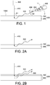
- FIG. 1 is referred, showing a device for measuring the thickness of a target ultrathin film 100, the target of the device and the measurement method discussed herein, on a substrate 300.
- a test sample 200 comprises the target ultrathin film 100 and the substrate 300.
- the method disclosed herein is a substrate assisted X-ray leakage method for ultrathin film thickness measurement (SAXRL).
- SAXRL substrate assisted X-ray leakage method for ultrathin film thickness measurement
- the thickness of the target ultrathin film 100 is measured from the intensities of the fluorescence X-ray 330 (i.e. the fluorescence X-ray intensities) converted by the substrate 300 and leaking or tunneling through the target ultrathin film 100 at various detection angle, such as a grazing detection angle ⁇ 2.
- the fluorescence X-ray 330 generated from the substrate 300 has sufficient and stable high intensity due to an ample substrate thickness about a millimeter instead of a few nanometers for the target thin film, therefore, can provide fluorescence signal strong enough to make the measurement performed rapidly and precisely.
- the method and the device disclosed herein can be used to measuring the thickness of a few nanometers (nm) or less of the target ultrathin film 100.
- the thickness of the target ultrathin film 100 which can be measured by the method and the device disclosed herein can be 0.2 nm to 2 nm.
- the target ultrathin film 100 having the thickness to be measured by the method and the device disclosed herein has X-ray scattering length density (SLD) preferably higher than the X-ray scattering length density of the substrate 300 under the target ultrathin film 100.
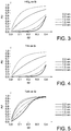
- the abovementioned substrate 300 can comprise a single material layer including a silicon wafer, a GaAs wafer, a InP wafer and/or other commonly encountered substrates, and the target ultrathin film 100 comprise a single material layer, as shown in FIG. 2A . Otherwise, the abovementioned substrate 300 can comprise multiple layers of different materials, and the target ultrathin film 100 can comprise a single material layer, as shown in FIG. 2B . Alternatively, the target ultrathin film 100 can comprise multiple layers of different materials.
- the abovementioned fluorescence X-ray 330 includes those from one or more layers comprising the substrate 300, or from one or more elements comprising the substrate 300.
- the target ultrathin film 100 and the substrate 300 may comprise semiconductor materials, but
- the device comprises a radiation source 400 and a fluorescence X-ray detector 500.
- the radiation source 400 is configured to project an excitation radiation 410 toward the upper surface 100S of the target ultrathin film 100 with an incident angle ⁇ 1 with respect to the upper surface 100S of the target ultrathin film 100, to generate fluorescence X-ray 330 from the substrate 300.
- the preferred range of ⁇ 1 is over 45° to 90°.
- the value of ⁇ 1 can be near 90°, i.e. near a normal incident direction.
- the excitation radiation 410 comprises an X-ray beam or an electron beam with their energy sufficiently high to excite desirable fluorescence X-ray 330 from one or more preselected substrate layers of the substrate 300.
- the fluorescence X-ray detector 500 is configured to measure a fluorescence X-ray 330 converted from the excitation radiation 410 by the substrate 300 with a grazing detection angle ⁇ 2 with respect to the upper surface 100S, over a preset grazing angular range.
- the fluorescence X-ray detector 500 is configured to receive the fluorescence X-ray 330 leaked through the target ultrathin film 100 over a range of the grazing detection angle ⁇ 2.
- the fluorescence X-ray detector 500 is capable of scanning through a preset angular range with an angular step of one hundredth or less of the angular range of ⁇ 2.
- a preferred ⁇ 2 angular range is between 0° and 2°, or beyond.
- the range of the grazing detection angle ⁇ 2 is chosen to be less than or comparable to the critical angle [2] of substrate/ thin film pairs commonly encountered in IC applications.
- the critical angle of an interface is dictated by the scattering length density of the materials across the interface as well as the wavelength of the substrate fluorescence X-ray.
- the fluorescence X-ray originated from the substrate can leak through the thin film of a few nanometers thick or less; whereas as ⁇ 2 becomes greater than the substrate/ thin film critical angle a majority of the fluorescence X-ray will leak through the thin film regardless of the film thickness, hence, renders a drop in its sensitivity of measuring film thickness.
- the abovementioned fluorescence X-ray detector 500 is capable of collecting fluorescence X-ray 330 over a range of energies or wavelengths simultaneously and quantifying the intensity distribution of the observed fluorescence X-ray 330 over the energy or wavelength window of interests.
- the fluorescence X-ray detector 500 is capable of discerning energies and/or wavelengths of the fluorescence X-ray observed, thereby, to collect the intensities of all selected fluorescence energies or wavelengths concurrently.
- the fluorescence X-ray intensities i.e. the intensities of the fluorescence X-ray 330
- the fluorescence X-ray detector 500 is capable of measuring a distribution of the fluorescence X-ray intensities (or the intensity distribution) as a function of the fluorescence wavelength or energy; thereby to selectively/concurrently measure the intensity (or the fluorescence X-ray intensities) originated from certain layers (e.g. one or more layers) and/ or certain elements (e.g. one or more elements) comprising the substrate 300, or from certain elements of a compound substrate such as InP, GaAs and/or others.
- the device further comprises a collimator 600 to define the angular resolution, ⁇ 2, of the measured fluorescence X-ray 330 leaked through the target ultrathin film 100.
- the collimator 600 is configured to enable a detection angular window or opening, ⁇ 2, at least a tenth of total angular range of ⁇ 2 or less.
- the collimator 600 is configured to be located between the test sample 200 and the fluorescence X-ray detector 500.
- the collimator 600 is configured to control the detection of the fluorescence X-ray 330 with an angular window of ⁇ 2 at any given grazing detection angle ⁇ 2.
- the collimator 600 can be installed in front of the fluorescence X-ray detector 500.
- Both the collimator 600 and the fluorescence X-ray detector 500 can be moved in unity over a present angular range of ⁇ 2 with an angular step size less than ⁇ 2 defined by the collimator 600.
- the collimator 600 may comprise a 1D collimator or a 2D collimator, which has pin holes and silts respectively.
- the thickness of the target ultrathin film 100 is calculated based on an angular dependence of measured fluorescence X-ray intensities of the fluorescence X-ray 330, after the said intensity being normalized with the fluorescence intensity measured in the absence of the target ultrathin film 100 at the abovementioned ⁇ 2.
- the well- established algorithm by Parratt [3] will be used to deduce film thickness from the angular dependence of the measured fluorescence intensity.
- the viable range of the thickness of the thin film can be pre-determined so as to be set as the boundary of the thickness for SAXRL measurements for any given substrate-thin film pairs of known composition and density.
- the simulation data of the grazing detection angles ⁇ 2 from 0 degree to the ending point can be used, wherein the intensity of the fluorescence X-ray 330 corresponding to the ending point and having the maximum value is normalized as the value of 1.
- the simulation data is calculated to obtain an optimal observation angle at which the intensities of the fluorescence X-ray 330 for the target ultrathin film 100 of different thickness have the maximum difference therebetween.
- the thickness of the target ultrathin film 100 to be really measured can be deduced by fitting the real measured data at the observation angles (grazing detection angles ⁇ 2) via the recursive Parratt algorithm.
- the thickness of the target ultrathin film 100 after being measured can be obtained by finding out the one curve of the simulation data which is the most close to and has the least square error relative to the curve of the simulation.
- the thickness measurement method according to the present disclosure can be applied into in-line product measurement without using standard samples, and therefore the thickness of the product can be measured rapidly and efficiently.
- the simulation data comprises a simulation curve obtained using the Parratt algorithm.
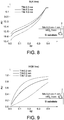
- FIG. 3 shows the simulation curves, of the target ultrathin film 100 consisting of HfO 2 having the thickness of 0.2nm, 0.5nm, 1.0nm, 1.5nm, and 2.0nm respectively on the substrate 300 consisting of Si, of the normalized intensity (i.e. the maximum intensity as 1) of the fluorescence X-ray 330 versus the detection angles ⁇ 2.
- the normalized intensity i.e. the maximum intensity as 1
- FIG. 4 shows the simulation curves, of the target ultrathin film 100 consisting of TiN having the thickness of 0.2nm, 0.5nm, 1.0nm, 1.5nm, and 2.0nm respectively on the substrate 300 consisting of Si, of the normalized intensity of the fluorescence X-ray 330 versus the detection angles ⁇ 2.
- the target ultrathin film 100 consisting of TiN having the thickness of 0.2nm, 0.5nm, 1.0nm, 1.5nm, and 2.0nm respectively on the substrate 300 consisting of Si
- the normalized intensity of the fluorescence X-ray 330 versus the detection angles ⁇ 2.
- FIG. 5 shows the simulation curves, of the target ultrathin film 100 consisting of TaN having the thickness of 0.2nm, 0.5nm, 1.0nm, 1.5nm, and 2.0nm respectively on the substrate 300 consisting of Si, of the normalized intensity of the fluorescence X-ray 330 versus the detection angles ⁇ 2.
- the SAXRL sensitivity among HfO 2 , TiN and TaN films while the probe is Silicon K-line. This difference can be explained by the quantity (SLD film - SLD substrate ) 0.5 [2] which is proportional to the critical angle of the film/substrate interface.
- the SLD of TiN and HfO 2 at the Silicon K-line energy is significantly greater than that of TaN; all three compounds have their SLD higher than that of Silicon.
- the small SLD of TaN dictates a small critical angle at the TaN /Si interface, hence, a small viable ⁇ 2 range for SAXRL.
- Table 1 further indicates that the SLD of TaN increases significantly as the probe is the fluorescence X-rays from either InP or GaAs.
- the cases of TaN on InP will be provided on FIG. 16 and FIG. 17 to highlight the impact of the probe wavelength on the sensitivity of SAXRL.
- the ending angle of the simulation curve is selected as the detection angle ⁇ 2 at which the normalized intensity of the leaked fluorescence 300 has the maximum value (i.e. about 1). The ending angle depends on the thickness and material of the target ultrathin film 100 to be measured, and the material of the substrate 300.
- the thickness of the target ultrathin film 100 of the test sample 200 can be calculated by fitting the experimental curve using the recursive Parratt algorithm without relying on reference samples with known thickness.
- FIG. 6 shows the simulation curves, of the target ultrathin film 100 consisting of HfO 2 having the thickness of 0.9nm, 1.0nm, 1.1nm on the substrate 300 consisting of Si, of the normalized intensity of the fluorescence X-ray 330 versus the detection angles ⁇ 2.
- the target ultrathin films 100 consisting of HfO 2 having the thicknesses of 0.9nm and 1.0nm a difference of merely 0.1 nm in the film thickness, an optimal observation angle of 0.277 degrees provides a good sensitivity of 6.22% in terms of the difference in the observed fluorescence intensity.
- the sensitivity is also 5.44%.
- FIG. 7 shows the simulation curves, of the target ultrathin film 100 consisting of HfO 2 having the thickness of 0.2nm, 0.3nm, 0.4nm on the substrate 300 consisting of Si, of the normalized intensity of the fluorescence X-ray 330 versus the detection angles ⁇ 2.
- the target ultrathin films 100 consisting of HfO 2 having the thicknesses of 0.2nm and 0.3nm a difference of merely 0.1 nm in the film thickness, the observation angle of 0.113 degrees provides a good sensitivity of 10.0% in terms of the difference in the leaked fluorescence intensity.
- the observation angle of 1.33 degrees provides a good sensitivity of 10.87%.
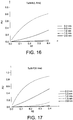
- FIG. 8 shows the simulation curves, for the TiN film on a HfO 2 / Silicon substrate with the film thickness of 0.2nm, 0.5nm, 1.0nm, of the normalized intensity of the Silicon K-line fluorescence X-ray 330 versus the to the detection angles ⁇ 2.
- the HfO 2 layer between the top film TiN and Silicon substrate has a thickness of 3 nm.
- FIG. 9 shows the simulation curves, of the target ultrathin film 100 consisting of TiN having the thickness of 0.2nm, 0.5nm, 1.0nm on the substrate 300 consisting of a 3 nm HfO 2 layer and a Silicon substrate, of the normalized intensity of the fluorescence X-ray 330 (M line of Hf) versus the detection angles ⁇ 2.
- M line of Hf normalized intensity of the fluorescence X-ray 330
- FIG. 10 shows the simulation curves, of the target ultrathin film 100 consisting of TaN having the thickness of 0.2nm, 0.47nm on the substrate 300 consisting of Si, of the normalized intensity of the Silicon K-line fluorescence X-ray 330 versus the detection angles ⁇ 2.
- the optimal observation angle is 0.092 degrees where the sensitivity is 5.17%.
- FIG. 11 shows the simulation curves, of the target ultrathin film 100 consisting of TaN having the thickness of 0.5nm, 0.77nm on the substrate 300 consisting of Si, of the normalized intensity of the Silicon K-line fluorescence X-ray 330 versus the detection angles ⁇ 2.
- the optimal observation angle is 0.092 degrees.
- FIG. 12 shows the simulation curves, of the target ultrathin film 100 consisting of HfO 2 having the thickness of 0.2nm, 0.5nm, 1.0nm, 1.5nm, 2.0nm on the substrate 300 consisting of GaAs, of the normalized intensity of the fluorescence X-ray 330 (Ga L-line of GaAs) versus the detection angles ⁇ 2.
- FIG. 13 shows the simulation curves, of the target ultrathin film 100 consisting of HfO 2 having the thickness of 0.2nm, 0.5nm, 1.0nm, 1.5nm, 2.0nm on the substrate 300 consisting of GaAs, of the normalized intensity of the fluorescence X-ray 330 (As L-line of GaAs) versus the detection angles ⁇ 2.
- the results given in this figure and in the figures above illustrate that the fluorescence from both the elements in a compound substrate can be used as the probe for film thickness.
- the fluorescence X-ray detector specified herein enables a simultaneous measurement of all the fluorescence X-rays of interests, i.e.
- FIG. 14 shows the simulation curves, of the target ultrathin film 100 consisting of HfO 2 having the thickness of 0.2nm, 0.5nm, 1.0nm, 1.5nm, 2.0nm on the substrate 300 consisting of InP, of the normalized intensity of the fluorescence X-ray 330 (In L-line of InP) versus the detection angles ⁇ 2.
- FIG. 15 shows the simulation curves, of the target ultrathin film 100 consisting of HfO 2 having the thickness of 0.2nm, 0.5nm, 1.0nm, 1.5nm, 2.0nm on the substrate 300 consisting of InP, of the normalized intensity of the fluorescence X-ray 330 (P K-line of InP) versus the detection angles ⁇ 2.
- the results given in this figure and in the figure above illustrate once again that the fluorescence from both the elements in a compound substrate can be used as the probe for film thickness.
- FIG. 16 shows the simulation curves, of the target ultrathin film 100 consisting of TaN having the thickness of 0.2nm, 0.5nm, 1.0nm, 1.5nm, 2.0nm on the substrate 300 consisting of InP, of the normalized intensity of the fluorescence X-ray 330 (In L-line of InP) versus the detection angles ⁇ 2.
- FIG. 17 shows the simulation curves, of the target ultrathin film 100 consisting of TaN having the thickness of 0.2nm, 0.5nm, 1.0nm, 1.5nm, 2.0nm on the substrate 300 consisting of InP, of the normalized intensity of the fluorescence X-ray 330 (P K-line of InP) versus the detection angles ⁇ 2.
- the results given in this figure and in the figure above illustrate once again that the fluorescence from both the elements in a compound substrate can be used as the probe for film thickness.
- the fluorescence from InP provides an improved SAXRL sensitivity.
- the scattering length densities (SLD) of the different film materials (i.e. Si, TiN, HfO 2 , TaN, Ti) of the test sample 200, and the characteristic fluorescence of the substrate materials are listed in table 1.
- the unit of the SLD is 1/ ⁇ 2 and the magnitude of SLD shows a weak dependence of the probing wavelength except for the TaN case.
- Table 1 substrate Si substrate GaAs substrate GaAs substrate InP substrate InP substrate fluorescence Si K-line of 1739eV/7. 129 ⁇ Ga L-line of 1097.9eV/ 11.2925 ⁇ As L-line of 1282eV/9.67 083 ⁇ In L-line of 3296.9eV/ 3.7605 ⁇ P K-line of 2013eV/6.
Landscapes
- Physics & Mathematics (AREA)
- General Physics & Mathematics (AREA)
- Electromagnetism (AREA)
- Analytical Chemistry (AREA)
- Life Sciences & Earth Sciences (AREA)
- Chemical & Material Sciences (AREA)
- Health & Medical Sciences (AREA)
- Biochemistry (AREA)
- General Health & Medical Sciences (AREA)
- Immunology (AREA)
- Pathology (AREA)
- Analysing Materials By The Use Of Radiation (AREA)
- Length-Measuring Devices Using Wave Or Particle Radiation (AREA)
Abstract
Description
- The application relates generally to a device and a method applicable for measuring a thickness of an ultrathin film on a substrate.
- The semiconductor integrated circuit (IC) industry has experienced rapid growth. Technological advances in IC materials and design have produced generations of ICs. Each generation has smaller and more complex circuits than the previous generation. In the course of IC evolution, functional density (i.e., the number of interconnected devices per chip area) has generally increased while geometric size (i.e., the smallest component (or line) that can be created using a fabrication process) has decreased. This scaling-down process generally provides benefits by increasing production efficiency and lowering associated costs. However, these advances have increased the complexity of processing and manufacturing ICs. Since feature sizes continue to decrease, fabrication and measurement processes continue to become more difficult to perform.
- In the past, common methods for detecting film thickness are X-ray reflectivity (XRR) and X-ray fluorescence (XRF) [1], but the measurement of ultra-thin film encountered some challenges. The XRR technique has the disadvantage of high noise ratio resulted from the high detecting angle required for measuring the thickness of the thin film thinner than about 1 nm. The XRF technique has the disadvantage of long measurement time due to the minuscular sample volume, hence, weak fluorescence signals for films thinner than about 1 nm. In addition, standard samples of known thickness need to be prepared, measured and then to establish calibration curves for the XRF measurement for thin film thickness.
- Therefore, a novel measurement technique satisfying requirements of both high efficiency and non-destructive is needed.
-
- Reference [1]: " Grazing incidence X-ray fluorescence analysis" A.lidaK.SakuraiA.YoshinagaY.Gohshi, Nucl. Instrum. Methods Phys. Res. A., 246, 736(1986).
- Reference [2]: ISBN 90-247-3418-5, "Theory of Reflection", John Lekner, (1987).
- Reference [3]: " Surface Studies of Solids by Total Reflection of X-Rays", L. G. Parratt, Phys. Rev. 95, 359 (1954).
- Reference [4]: The
US patent no. 6,263,042 , entitled as "Apparatus for X-ray analysis in grazing exit conditions", relates to technique of grazing exit X-ray fluorescence (GEXRF). - According to one embodiment of this disclosure, what is provided is a device for measuring the thickness of an ultrathin film, the target of the device and the measurement method discussed herein, on a solid substrate. The device comprises a radiation source and a fluorescence X-ray detector. The radiation source is configured to project an excitation radiation toward the upper surface of the target ultrathin film with an incident angle θ1 with respect to the upper film surface, wherein the value of θ1 can be near 90°, i.e. near a normal incident direction. The fluorescence X-ray detector is configured to measure a fluorescence X-ray converted from the excitation radiation by the substrate with a grazing detection angle θ2 with respect to the target ultrathin film surface, over a preset grazing angular range. A wavelength or an energy dispersive detector is an essential part of this invention; it will enable the selection of a suitable the characteristic fluorescence X-ray from the substrate layers as the probe of the film thickness. In general, fluorescence with long wavelength is preferred over those with short wavelength.
- According to another embodiment of this disclosure, what is provided is a method for measuring a thickness of an ultrathin film over a substrate, comprising: projecting a excitation radiation toward an upper surface of the target ultrathin film with an incident angle θ1 with respect to the upper surface of the target ultrathin film, wherein preferred range of θ1 is over 45° to 90°; and detecting a fluorescence X-ray converted from the excitation radiation by the substrate with a grazing detection angle θ2 defined with respect to the upper surface of the target ultrathin film, wherein the preferred angular range is 2°≥ θ2≥ 0°.
- The above and other aspects of this disclosure will become better understood with regard to the following detailed description of the preferred but non-limiting embodiments. The following description is made with reference to the accompanying drawings.
-
-
FIG. 1 shows a device for measuring a thickness of an ultrathin film on a substrate according to one embodiment. -
FIG. 2A shows a method for measuring a thickness of an ultrathin film on a substrate according to one embodiment. -
FIG. 2B shows a method for measuring a thickness of an ultrathin film on a two-layer substrate according to one embodiment. -
FIG. 3 shows the simulation curves, of the target ultrathin film consisting of HfO2 having the thickness of 0.2nm, 0.5nm, 1.0nm, 1.5nm, and 2.0nm respectively on the substrate consisting of Si, of the normalized intensity of the fluorescence versus the detection angles θ2. -
FIG. 4 shows the simulation curves, of the target ultrathin film consisting of TiN having the thickness of 0.2nm, 0.5nm, 1.0nm, 1.5nm, and 2.0nm respectively on the substrate consisting of Si, of the normalized intensity of the fluorescence versus the detection angles θ2. -
FIG. 5 shows the simulation curves, of the target ultrathin film consisting of TaN having the thickness of 0.2nm, 0.5nm, 1.0nm, 1.5nm, and 2.0nm respectively on the substrate consisting of Si, of the normalized intensity of the fluorescence versus the detection angles θ2. -
FIG. 6 shows the simulation curves, of the target ultrathin film consisting of HfO2 having the thickness of 0.9nm, 1.0nm, 1.1nm on the substrate consisting of Si, of the normalized intensity of the fluorescence versus the detection angles θ2. -
FIG. 7 shows the simulation curves, of the target ultrathin film consisting of HfO2 having the thickness of 0.2nm, 0.3nm, 0.4nm on the substrate consisting of Si, of the normalized intensity of the fluorescence to the detection angles θ2. -
FIG. 8 shows the simulation curves, for the TiN film having the thickness of 0.2nm, 0.5nm, 1.0nm on a HfO2/Silicon substrate, of the normalized intensity of the Silicon K-line fluorescence versus the detection angles θ2. -
FIG. 9 shows the simulation curves, of the target ultrathin film consisting of TiN having the thickness of 0.2nm, 0.5nm, 1.0nm on a substrate consisting of HfO2/Si substrate, of the normalized intensity of the fluorescence (Hf M-line) versus the detection angles θ2. -
FIG. 10 shows the simulation curves, of the target ultrathin film consisting of TaN having the thickness of 0.2nm, 0.47nm on the substrate consisting of Si, of the normalized intensity of the Silicon K-line fluorescence versus the detection angles θ2. -
FIG. 11 shows the simulation curves, of the target ultrathin film consisting of TaN having the thickness of 0.5nm, 0.77nm on the substrate consisting of Si, of the normalized intensity of the Silicon K-line fluorescence versus the detection angles θ2. -
FIG. 12 shows the simulation curves, of the target ultrathin film consisting of HfO2 having the thickness of 0.2nm, 0.5nm, 1.0nm, 1.5nm, 2.0nm on the substrate consisting of GaAs, of the normalized intensity of the fluorescence (Ga L-line) of GaAs versus the detection angles θ2. -
FIG. 13 shows the simulation curves, of the target ultrathin film consisting of HfO2 having the thickness of 0.2nm, 0.5nm, 1.0nm, 1.5nm, 2.0nm on the substrate consisting of GaAs, of the normalized intensity of the fluorescence (As L-line) of GaAs versus the detection angles θ2. -
FIG. 14 shows the simulation curves, of the target ultrathin film consisting of HfO2 having the thickness of 0.2nm, 0.5nm, 1.0nm, 1.5nm, 2.0nm on the substrate consisting of InP, of the normalized intensity of the fluorescence (In L-line) of InP versus the detection angles θ2. -
FIG. 15 shows the simulation curves, of the target ultrathin film consisting of HfO2 having the thickness of 0.2nm, 0.5nm, 1.0nm, 1.5nm, 2.0nm on the substrate consisting of InP, of the normalized intensity of the fluorescence (P K-line) of InP) versus the detection angles θ2. -
FIG. 16 shows the simulation curves, of the target ultrathin film consisting of TaN having the thickness of 0.2nm, 0.5nm, 1.0nm, 1.5nm, and 2.0nm respectively on a InP substrate, of the normalized intensity of the In L-line fluorescence versus the detection angles θ2. -
FIG. 17 shows the simulation curves, of the target ultrathin film consisting of TaN having the thickness of 0.2nm, 0.5nm, 1.0nm, 1.5nm, and 2.0nm respectively on a InP substrate, of the normalized intensity of the P K-line fluorescence versus the detection angles θ2. - In the following detailed description, for purposes of explanation, numerous specific details are set forth in order to provide a thorough understanding of the disclosed embodiments. It will be apparent, however, that one or more embodiments may be practiced without these specific details. In other instances, well-known structures and devices are schematically shown in order to simplify the drawing.
-
FIG. 1 is referred, showing a device for measuring the thickness of atarget ultrathin film 100, the target of the device and the measurement method discussed herein, on asubstrate 300. Atest sample 200 comprises thetarget ultrathin film 100 and thesubstrate 300. The method disclosed herein is a substrate assisted X-ray leakage method for ultrathin film thickness measurement (SAXRL). The thickness of thetarget ultrathin film 100 is measured from the intensities of the fluorescence X-ray 330 (i.e. the fluorescence X-ray intensities) converted by thesubstrate 300 and leaking or tunneling through thetarget ultrathin film 100 at various detection angle, such as a grazing detection angle θ2. Thefluorescence X-ray 330 generated from thesubstrate 300 has sufficient and stable high intensity due to an ample substrate thickness about a millimeter instead of a few nanometers for the target thin film, therefore, can provide fluorescence signal strong enough to make the measurement performed rapidly and precisely. The method and the device disclosed herein can be used to measuring the thickness of a few nanometers (nm) or less of the targetultrathin film 100. The thickness of the targetultrathin film 100 which can be measured by the method and the device disclosed herein can be 0.2 nm to 2 nm. The targetultrathin film 100 having the thickness to be measured by the method and the device disclosed herein has X-ray scattering length density (SLD) preferably higher than the X-ray scattering length density of thesubstrate 300 under the targetultrathin film 100. Theabovementioned substrate 300 can comprise a single material layer including a silicon wafer, a GaAs wafer, a InP wafer and/or other commonly encountered substrates, and the targetultrathin film 100 comprise a single material layer, as shown inFIG. 2A . Otherwise, theabovementioned substrate 300 can comprise multiple layers of different materials, and the targetultrathin film 100 can comprise a single material layer, as shown inFIG. 2B . Alternatively, the targetultrathin film 100 can comprise multiple layers of different materials. Theabovementioned fluorescence X-ray 330 includes those from one or more layers comprising thesubstrate 300, or from one or more elements comprising thesubstrate 300. The targetultrathin film 100 and thesubstrate 300 may comprise semiconductor materials, but are not limited thereto. - The device comprises a
radiation source 400 and afluorescence X-ray detector 500. - The
radiation source 400 is configured to project anexcitation radiation 410 toward theupper surface 100S of the targetultrathin film 100 with an incident angle θ1 with respect to theupper surface 100S of the targetultrathin film 100, to generatefluorescence X-ray 330 from thesubstrate 300. The preferred range of θ1 is over 45° to 90°. The value of θ1 can be near 90°, i.e. near a normal incident direction. Theexcitation radiation 410 comprises an X-ray beam or an electron beam with their energy sufficiently high to excitedesirable fluorescence X-ray 330 from one or more preselected substrate layers of thesubstrate 300. - The
fluorescence X-ray detector 500 is configured to measure afluorescence X-ray 330 converted from theexcitation radiation 410 by thesubstrate 300 with a grazing detection angle θ2 with respect to theupper surface 100S, over a preset grazing angular range. Thefluorescence X-ray detector 500 is configured to receive thefluorescence X-ray 330 leaked through the targetultrathin film 100 over a range of the grazing detection angle θ2. Thefluorescence X-ray detector 500 is capable of scanning through a preset angular range with an angular step of one hundredth or less of the angular range of θ2. A preferred θ2 angular range is between 0° and 2°, or beyond. The range of the grazing detection angle θ2 is chosen to be less than or comparable to the critical angle [2] of substrate/ thin film pairs commonly encountered in IC applications. The critical angle of an interface is dictated by the scattering length density of the materials across the interface as well as the wavelength of the substrate fluorescence X-ray. At θ2 less than the substrate/ thin film critical angle the fluorescence X-ray originated from the substrate can leak through the thin film of a few nanometers thick or less; whereas as θ2 becomes greater than the substrate/ thin film critical angle a majority of the fluorescence X-ray will leak through the thin film regardless of the film thickness, hence, renders a drop in its sensitivity of measuring film thickness. The abovementionedfluorescence X-ray detector 500 is capable of collectingfluorescence X-ray 330 over a range of energies or wavelengths simultaneously and quantifying the intensity distribution of the observedfluorescence X-ray 330 over the energy or wavelength window of interests. Thefluorescence X-ray detector 500 is capable of discerning energies and/or wavelengths of the fluorescence X-ray observed, thereby, to collect the intensities of all selected fluorescence energies or wavelengths concurrently. The fluorescence X-ray intensities (i.e. the intensities of the fluorescence X-ray 330) are detected with a plurality of the grazing detection angles θ2. Thefluorescence X-ray detector 500 is capable of measuring a distribution of the fluorescence X-ray intensities (or the intensity distribution) as a function of the fluorescence wavelength or energy; thereby to selectively/concurrently measure the intensity (or the fluorescence X-ray intensities) originated from certain layers (e.g. one or more layers) and/ or certain elements (e.g. one or more elements) comprising thesubstrate 300, or from certain elements of a compound substrate such as InP, GaAs and/or others. - The device further comprises a
collimator 600 to define the angular resolution, δθ2, of the measuredfluorescence X-ray 330 leaked through the targetultrathin film 100. Thecollimator 600 is configured to enable a detection angular window or opening, δθ2, at least a tenth of total angular range of θ2 or less. Thecollimator 600 is configured to be located between thetest sample 200 and thefluorescence X-ray detector 500. Thecollimator 600 is configured to control the detection of thefluorescence X-ray 330 with an angular window of δθ2 at any given grazing detection angle θ2. Thecollimator 600 can be installed in front of thefluorescence X-ray detector 500. Both thecollimator 600 and thefluorescence X-ray detector 500 can be moved in unity over a present angular range of θ2 with an angular step size less than δθ2 defined by thecollimator 600. Thecollimator 600 may comprise a 1D collimator or a 2D collimator, which has pin holes and silts respectively. - The thickness of the target
ultrathin film 100 is calculated based on an angular dependence of measured fluorescence X-ray intensities of thefluorescence X-ray 330, after the said intensity being normalized with the fluorescence intensity measured in the absence of the targetultrathin film 100 at the abovementioned θ2. The well- established algorithm by Parratt [3] will be used to deduce film thickness from the angular dependence of the measured fluorescence intensity. Using Parratt algorithm the viable range of the thickness of the thin film can be pre-determined so as to be set as the boundary of the thickness for SAXRL measurements for any given substrate-thin film pairs of known composition and density. The simulation data of the grazing detection angles θ2 from 0 degree to the ending point can be used, wherein the intensity of thefluorescence X-ray 330 corresponding to the ending point and having the maximum value is normalized as the value of 1. The simulation data is calculated to obtain an optimal observation angle at which the intensities of thefluorescence X-ray 330 for the targetultrathin film 100 of different thickness have the maximum difference therebetween. The thickness of the targetultrathin film 100 to be really measured can be deduced by fitting the real measured data at the observation angles (grazing detection angles θ2) via the recursive Parratt algorithm. Alternatively, the thickness of the targetultrathin film 100 after being measured can be obtained by finding out the one curve of the simulation data which is the most close to and has the least square error relative to the curve of the simulation. The thickness measurement method according to the present disclosure can be applied into in-line product measurement without using standard samples, and therefore the thickness of the product can be measured rapidly and efficiently. - The simulation data comprises a simulation curve obtained using the Parratt algorithm.
FIG. 3 shows the simulation curves, of the targetultrathin film 100 consisting of HfO2 having the thickness of 0.2nm, 0.5nm, 1.0nm, 1.5nm, and 2.0nm respectively on thesubstrate 300 consisting of Si, of the normalized intensity (i.e. the maximum intensity as 1) of thefluorescence X-ray 330 versus the detection angles θ2. A respectful sensitivity of discerning film thickness between 0.2 nm to 2 nm is demonstrated. -
FIG. 4 shows the simulation curves, of the targetultrathin film 100 consisting of TiN having the thickness of 0.2nm, 0.5nm, 1.0nm, 1.5nm, and 2.0nm respectively on thesubstrate 300 consisting of Si, of the normalized intensity of thefluorescence X-ray 330 versus the detection angles θ2. A respectful sensitivity of discerning film thickness between 0.2 nm to 2 nm is demonstrated. -
FIG. 5 shows the simulation curves, of the targetultrathin film 100 consisting of TaN having the thickness of 0.2nm, 0.5nm, 1.0nm, 1.5nm, and 2.0nm respectively on thesubstrate 300 consisting of Si, of the normalized intensity of thefluorescence X-ray 330 versus the detection angles θ2. As illustrated byfigures 3-5 there exists a noticeable difference in the SAXRL sensitivity among HfO2, TiN and TaN films while the probe is Silicon K-line. This difference can be explained by the quantity (SLDfilm- SLDsubstrate)0.5 [2] which is proportional to the critical angle of the film/substrate interface. Based on the data given in Table 1 the SLD of TiN and HfO2 at the Silicon K-line energy is significantly greater than that of TaN; all three compounds have their SLD higher than that of Silicon. The small SLD of TaN dictates a small critical angle at the TaN /Si interface, hence, a small viable θ2 range for SAXRL. Table 1 further indicates that the SLD of TaN increases significantly as the probe is the fluorescence X-rays from either InP or GaAs. The cases of TaN on InP will be provided onFIG. 16 and FIG. 17 to highlight the impact of the probe wavelength on the sensitivity of SAXRL. - It is observed that as the thickness of the target
ultrathin film 100 increases, the intensity of thefluorescence X-ray 330 originated from thesubstrate 300 and leaked through the target ultrathin film decreases, and vice versa. The ending angle of the simulation curve is selected as the detection angle θ2 at which the normalized intensity of the leakedfluorescence 300 has the maximum value (i.e. about 1). The ending angle depends on the thickness and material of the targetultrathin film 100 to be measured, and the material of thesubstrate 300. - The thickness of the target
ultrathin film 100 of thetest sample 200 can be calculated by fitting the experimental curve using the recursive Parratt algorithm without relying on reference samples with known thickness. -
FIG. 6 shows the simulation curves, of the targetultrathin film 100 consisting of HfO2 having the thickness of 0.9nm, 1.0nm, 1.1nm on thesubstrate 300 consisting of Si, of the normalized intensity of thefluorescence X-ray 330 versus the detection angles θ2. For the targetultrathin films 100 consisting of HfO2 having the thicknesses of 0.9nm and 1.0nm, a difference of merely 0.1 nm in the film thickness, an optimal observation angle of 0.277 degrees provides a good sensitivity of 6.22% in terms of the difference in the observed fluorescence intensity. For HfO2 films with their thicknesses of 1.0nm and 1.1nm, the sensitivity is also 5.44%. -
FIG. 7 shows the simulation curves, of the targetultrathin film 100 consisting of HfO2 having the thickness of 0.2nm, 0.3nm, 0.4nm on thesubstrate 300 consisting of Si, of the normalized intensity of thefluorescence X-ray 330 versus the detection angles θ2. For the targetultrathin films 100 consisting of HfO2 having the thicknesses of 0.2nm and 0.3nm, a difference of merely 0.1 nm in the film thickness, the observation angle of 0.113 degrees provides a good sensitivity of 10.0% in terms of the difference in the leaked fluorescence intensity. For HfO2 films with their thicknesses of 0.3nm and 0.4nm, the observation angle of 1.33 degrees provides a good sensitivity of 10.87%. -
FIG. 8 shows the simulation curves, for the TiN film on a HfO2 / Silicon substrate with the film thickness of 0.2nm, 0.5nm, 1.0nm, of the normalized intensity of the Silicon K-line fluorescence X-ray 330 versus the to the detection angles θ2. The HfO2 layer between the top film TiN and Silicon substrate has a thickness of 3 nm. -
FIG. 9 shows the simulation curves, of the targetultrathin film 100 consisting of TiN having the thickness of 0.2nm, 0.5nm, 1.0nm on thesubstrate 300 consisting of a 3 nm HfO2 layer and a Silicon substrate, of the normalized intensity of the fluorescence X-ray 330 (M line of Hf) versus the detection angles θ2. The results presented in this figure are dramatically different from that ofFIG. 8 ; this difference highlights the impact of choosing different fluorescence spectrum as the probe. -
FIG. 10 shows the simulation curves, of the targetultrathin film 100 consisting of TaN having the thickness of 0.2nm, 0.47nm on thesubstrate 300 consisting of Si, of the normalized intensity of the Silicon K-line fluorescence X-ray 330 versus the detection angles θ2. The optimal observation angle is 0.092 degrees where the sensitivity is 5.17%.FIG. 11 shows the simulation curves, of the targetultrathin film 100 consisting of TaN having the thickness of 0.5nm, 0.77nm on thesubstrate 300 consisting of Si, of the normalized intensity of the Silicon K-line fluorescence X-ray 330 versus the detection angles θ2. The optimal observation angle is 0.092 degrees. -
FIG. 12 shows the simulation curves, of the targetultrathin film 100 consisting of HfO2 having the thickness of 0.2nm, 0.5nm, 1.0nm, 1.5nm, 2.0nm on thesubstrate 300 consisting of GaAs, of the normalized intensity of the fluorescence X-ray 330 (Ga L-line of GaAs) versus the detection angles θ2. -
FIG. 13 shows the simulation curves, of the targetultrathin film 100 consisting of HfO2 having the thickness of 0.2nm, 0.5nm, 1.0nm, 1.5nm, 2.0nm on thesubstrate 300 consisting of GaAs, of the normalized intensity of the fluorescence X-ray 330 (As L-line of GaAs) versus the detection angles θ2. The results given in this figure and in the figures above illustrate that the fluorescence from both the elements in a compound substrate can be used as the probe for film thickness. Note that the fluorescence X-ray detector specified herein enables a simultaneous measurement of all the fluorescence X-rays of interests, i.e. a single θ2 scan suffices to collect data of both Ga L-line and As L-line as illustrated inFIG. 12 and FIG. 13 . The above statement holds true also for the cases of multiple layers substrate such as what illustrated inFIG. 8 and FIG. 9 as well as other compound substrates such as In P. -
FIG. 14 shows the simulation curves, of the targetultrathin film 100 consisting of HfO2 having the thickness of 0.2nm, 0.5nm, 1.0nm, 1.5nm, 2.0nm on thesubstrate 300 consisting of InP, of the normalized intensity of the fluorescence X-ray 330 (In L-line of InP) versus the detection angles θ2. -
FIG. 15 shows the simulation curves, of the targetultrathin film 100 consisting of HfO2 having the thickness of 0.2nm, 0.5nm, 1.0nm, 1.5nm, 2.0nm on thesubstrate 300 consisting of InP, of the normalized intensity of the fluorescence X-ray 330 (P K-line of InP) versus the detection angles θ2. The results given in this figure and in the figure above illustrate once again that the fluorescence from both the elements in a compound substrate can be used as the probe for film thickness. -
FIG. 16 shows the simulation curves, of the targetultrathin film 100 consisting of TaN having the thickness of 0.2nm, 0.5nm, 1.0nm, 1.5nm, 2.0nm on thesubstrate 300 consisting of InP, of the normalized intensity of the fluorescence X-ray 330 (In L-line of InP) versus the detection angles θ2. -
FIG. 17 shows the simulation curves, of the targetultrathin film 100 consisting of TaN having the thickness of 0.2nm, 0.5nm, 1.0nm, 1.5nm, 2.0nm on thesubstrate 300 consisting of InP, of the normalized intensity of the fluorescence X-ray 330 (P K-line of InP) versus the detection angles θ2. The results given in this figure and in the figure above illustrate once again that the fluorescence from both the elements in a compound substrate can be used as the probe for film thickness. In comparison to the result given inFIG. 5 , where Silicon is the substrate, the fluorescence from InP provides an improved SAXRL sensitivity. - The scattering length densities (SLD) of the different film materials (i.e. Si, TiN, HfO2, TaN, Ti) of the
test sample 200, and the characteristic fluorescence of the substrate materials are listed in table 1. The unit of the SLD is 1/Å2 and the magnitude of SLD shows a weak dependence of the probing wavelength except for the TaN case.Table 1 substrate Si substrate GaAs substrate GaAs substrate InP substrate InP substrate fluorescence Si K-line of 1739eV/7. 129Å Ga L-line of 1097.9eV/ 11.2925Å As L-line of 1282eV/9.67 083Å In L-line of 3296.9eV/ 3.7605Å P K-line of 2013eV/6. 15897Å Si 1.53E-05 1.81E-05 1.77E-05 2.02E-05 1.71E-05 TiN 4.15E-05 4.13E-05 4.16E-05 4.01 E-05 4.13E-05 HfO2 3.90E-05 4.65E-05 4.53E-05 6.46E-05 5.14E-05 TaN 1.97E-05 6.78E-05 6.68E-05 9.52E-05 7.03E-05 Ti 3.50E-05 3.46E-05 3.50E-05 3.36E-05 3.48E-05 - It will be apparent to those skilled in the art that various modifications and variations could be made to the disclosed embodiments. It is intended that the specification and examples be considered as exemplary only, with a true scope of the disclosure being indicated by the following claims and their equivalents.
Claims (22)
- A device for measuring a thickness of a target ultrathin film (100) on a substrate (300), and the device comprising:a radiation source (400) configured to project an excitation radiation (410) toward an upper surface (100S) of the target ultrathin film (100) with an incident angle θ1 with respect to the upper surface (100S), wherein the incident angle θ1 is near 90°; anda fluorescence X-ray detector (500) configured to measure a fluorescence X-ray (330) converted from the excitation radiation (410) by the substrate (300) with a grazing detection angle θ2 with respect to the upper surface (100S), over a preset grazing angular range.
- The device according to claim 1, wherein the target ultrathin film (100) has the thickness of a few nanometers (nm) or less.
- The device according to claim 1, wherein the thickness of the target ultrathin film (100) is 0.2 nm to 2 nm.
- The device according to claim 1, wherein an energy of the excitation radiation (410) is sufficiently high to excite the fluorescence X-ray (330) from the substrate (300).
- The device according to claim 1, wherein the excitation radiation (410) comprises an X-ray beam or an electron beam.
- The device according to claim 1, wherein the fluorescence X-ray detector (500) is capable of scanning through a preset angular range with an angular step less than or equal to one hundredth of the preset angular range, an angular range is between 0° and 2° or beyond.
- The device according to claim 1, further comprises a collimator (600) configured to enable a detection of angular window or opening δθ2 at least a tenth of total angular range of the grazing detection angle θ2 or less.
- The device according to claim 1, wherein the target ultrathin film (100) has an X-ray scattering length density higher than an X-ray scattering length density of the substrate (300).
- The device according to claim 7, wherein a test sample (200) comprises the target ultrathin film (100) and the substrate (300), the collimator (600) is configured to control a detection of the fluorescence X-ray (330) with the angular window or opening δθ2 at any given the grazing detection angle θ2.
- The device according to claim 9, wherein the collimator (600) is configured to be between the test sample (200) and the fluorescence X-ray detector (500).
- The device according to claim 8, wherein the substrate (300) comprises multiple layers of different materials or a single material layer including a silicon wafer, a GaAs wafer, or an InP wafer, the fluorescence X-ray (330) includes those from one or more layers comprising the substrate (300), or from one or more elements comprising the substrate (300).
- The device according to claim 1, wherein the fluorescence X-ray detector (500) is capable of discerning energies and/or wavelengths of the fluorescence X-ray (330) observed, thereby, to collect intensities of all of the fluorescence energies or wavelengths selected concurrently.
- A method for measuring a thickness of a target ultrathin film (100) over a substrate (300), comprising:projecting an excitation radiation (410) toward an upper surface (100S) of the target ultrathin film (100) with an incident angle θ1 with respect to the upper surface (100S) of the target ultrathin film (100), wherein a range of the incident angle θ1 is over 45° to 90°; anddetecting a fluorescence X-ray (330) converted from the excitation radiation (410) by the substrate (300) with a grazing detection angle θ2 defined with respect to the upper surface (100S) of the target ultrathin film (100), wherein the grazing detection angle θ2 is 2°≥ θ2≥ 0° or beyond.
- The method according to claim 13, wherein the excitation radiation (410) comprises an X-ray beam or an electron beam with its energy sufficiently high to excite the fluorescence X-ray (330) from one or more preselected element in layers of the substrate (300).
- The method according to claim 13, comprising detecting fluorescence X-ray intensities with a plurality of the grazing detection angles θ2, wherein a fluorescence X-ray detector (500) is capable of measuring a distribution of the fluorescence X-ray intensities as a function of a fluorescence wavelength or energy; thereby to concurrently measure the fluorescence X-ray intensities originated from one or more layers comprising the substrate (300) or from one or more elements of a compound substrate comprising InP, or GaAs.
- The method according to claim 13, comprising calculating the thickness of the target ultrathin film (100) based on an angular dependence of measured fluorescence X-ray intensities after the measured fluorescence X-ray intensities being normalized with a fluorescence X-ray intensity measured in the absence of the target ultrathin film (100) at the grazing detection angle θ2.
- The method according to claim 13, wherein the target ultrathin film (100) has the thickness less than a few nanometers.
- The method according to claim 13, wherein the thickness of the target ultrathin film (100) is 0.2nm to 2 nm.
- The method according to claim 13, further comprising a collimator (600) to define an angular resolution δθ2 of the fluorescence X-ray (330) measured and leaked through the target ultrathin film (100), the value of the angular resolution δθ2 is set to be at least a tenth of total angular range of the grazing detection angle θ2 or less.
- The method according to claim 13, further comprising a radiation source (400) and a fluorescence X-ray detector (500), wherein the radiation source (400) is configured to project the excitation radiation (410) to generate the fluorescence X-ray (330) from the substrate (300), the fluorescence X-ray detector (500) is configured to receive the fluorescence X-ray (330) leaked through the target ultrathin film (100) over a range of the grazing detection angle θ2.
- The method according to claim 20, wherein a device comprises a collimator (600) installed in front of the fluorescence X-ray detector (500), both the collimator (600) and the fluorescence X-ray detector (500) are capable of moving in unity over a present angular range of the grazing detection angle θ2 with an angular step size less than an angular resolution δθ2 defined by the collimator (600).
- The method according to claim 13, wherein the substrate (300) is either a single layer structure or a multi-layer structure.
Applications Claiming Priority (1)
| Application Number | Priority Date | Filing Date | Title |
|---|---|---|---|
| US16/730,236 US11287253B2 (en) | 2019-12-30 | 2019-12-30 | Device and method applicable for measuring ultrathin thickness of film on substrate |
Publications (2)
| Publication Number | Publication Date |
|---|---|
| EP3845893A1 true EP3845893A1 (en) | 2021-07-07 |
| EP3845893B1 EP3845893B1 (en) | 2022-12-21 |
Family
ID=70470863
Family Applications (1)
| Application Number | Title | Priority Date | Filing Date |
|---|---|---|---|
| EP20171530.7A Active EP3845893B1 (en) | 2019-12-30 | 2020-04-27 | System and method applicable for measuring thickness of ultrathin film on substrate |
Country Status (3)
| Country | Link |
|---|---|
| US (1) | US11287253B2 (en) |
| EP (1) | EP3845893B1 (en) |
| TW (1) | TWI761788B (en) |
Families Citing this family (5)
| Publication number | Priority date | Publication date | Assignee | Title |
|---|---|---|---|---|
| US11867595B2 (en) | 2019-10-14 | 2024-01-09 | Industrial Technology Research Institute | X-ray reflectometry apparatus and method thereof for measuring three dimensional nanostructures on flat substrate |
| WO2023067580A1 (en) * | 2021-10-24 | 2023-04-27 | Nova Measuring Instruments Inc. | Characterizing and measuring in small boxes using xps with multiple measurements |
| CN114061496B (en) * | 2021-11-23 | 2023-06-16 | 长江存储科技有限责任公司 | Method for measuring thickness of surface film layer of sample |
| TWI814579B (en) | 2022-09-13 | 2023-09-01 | 財團法人工業技術研究院 | X-ray reflectometry apparatus and method thereof for measuring three dimensional nanostructures on flat substrate |
| US12493004B2 (en) | 2022-09-28 | 2025-12-09 | Industrial Technology Research Institute | Method for determining parameters of three dimensional nanostructure and apparatus applying the same |
Citations (1)
| Publication number | Priority date | Publication date | Assignee | Title |
|---|---|---|---|---|
| US6263042B1 (en) | 1998-09-28 | 2001-07-17 | U.S. Philips Corporation | Apparatus for X-ray analysis in grazing exit conditions |
Family Cites Families (4)
| Publication number | Priority date | Publication date | Assignee | Title |
|---|---|---|---|---|
| US5778039A (en) | 1996-02-21 | 1998-07-07 | Advanced Micro Devices, Inc. | Method and apparatus for the detection of light elements on the surface of a semiconductor substrate using x-ray fluorescence (XRF) |
| US7277819B2 (en) | 2005-10-31 | 2007-10-02 | Eastman Kodak Company | Measuring layer thickness or composition changes |
| JP5712778B2 (en) | 2011-05-10 | 2015-05-07 | 信越半導体株式会社 | Method for measuring film thickness of SOI layer of SOI wafer |
| JP6290637B2 (en) | 2014-01-30 | 2018-03-07 | 浜松ホトニクス株式会社 | Film thickness measuring method and film thickness measuring apparatus |
-
2019
- 2019-12-30 US US16/730,236 patent/US11287253B2/en active Active
-
2020
- 2020-03-16 TW TW109108564A patent/TWI761788B/en active
- 2020-04-27 EP EP20171530.7A patent/EP3845893B1/en active Active
Patent Citations (1)
| Publication number | Priority date | Publication date | Assignee | Title |
|---|---|---|---|---|
| US6263042B1 (en) | 1998-09-28 | 2001-07-17 | U.S. Philips Corporation | Apparatus for X-ray analysis in grazing exit conditions |
Non-Patent Citations (7)
| Title |
|---|
| A.LIDAK.SAKURAIA.YOSHINAGAY.GOHSHI: "Grazing incidence X-ray fluorescence analysis", NUCL. INSTRUM. METHODS PHYS. RES. A., vol. 246, 1986, pages 736 |
| DE BOKX P K ET AL: "Grazing-emission X-ray fluorescence spectrometry; principles and applications", SPECTROCHIMICA ACTA. PART B: ATOMIC SPECTROSCOPY, vol. 52, no. 7, 1997, pages 829 - 840, XP085629886, ISSN: 0584-8547, DOI: 10.1016/S0584-8547(96)01644-8 * |
| JOHN LEKNER, THEORY OF REFLECTION, 1987, ISBN: 90-247-3418-5 |
| L. G. PARRATT: "Surface Studies of Solids by Total Reflection of X-Rays", PHYS. REV., vol. 95, 1954, pages 359, XP001002210, DOI: 10.1103/PhysRev.95.359 |
| TSUJI ET AL: "Grazing-exit electron probe X-ray microanalysis (GE-EPMA): Fundamental and applications", SPECTROCHIMICA ACTA. PART B: ATOMIC SPECTROSCOPY, NEW YORK, NY, US, US, vol. 60, no. 11, November 2005 (2005-11-01), pages 1381 - 1391, XP027717954, ISSN: 0584-8547, [retrieved on 20051101] * |
| TSUJI K ET AL: "New experimental equipment for grazing-exit electron-probe microanalysis", REVIEW OF SCIENTIFIC INSTRUMENTS, AIP, MELVILLE, NY, US, vol. 72, no. 10, October 2001 (2001-10-01), pages 3933 - 3936, XP012038856, ISSN: 0034-6748, DOI: 10.1063/1.1405788 * |
| ZOYA SPOLNIK ET AL: "Grazing-exit electron probe X-ray microanalysis of ultra-thin films and single particles with high-angle resolution", ANALYTICA CHIMICA ACTA, vol. 455, no. 2, March 2002 (2002-03-01), AMSTERDAM, NL, pages 245 - 252, XP055743423, ISSN: 0003-2670, DOI: 10.1016/S0003-2670(01)01601-4 * |
Also Published As
| Publication number | Publication date |
|---|---|
| US11287253B2 (en) | 2022-03-29 |
| TW202124941A (en) | 2021-07-01 |
| US20210199428A1 (en) | 2021-07-01 |
| EP3845893B1 (en) | 2022-12-21 |
| TWI761788B (en) | 2022-04-21 |
Similar Documents
| Publication | Publication Date | Title |
|---|---|---|
| EP3845893B1 (en) | System and method applicable for measuring thickness of ultrathin film on substrate | |
| US6381303B1 (en) | X-ray microanalyzer for thin films | |
| US11549895B2 (en) | System and method using x-rays for depth-resolving metrology and analysis | |
| Kobayashi et al. | High resolution-high energy x-ray photoelectron spectroscopy using third-generation synchrotron radiation source, and its application to Si-high k insulator systems | |
| US6816570B2 (en) | Multi-technique thin film analysis tool | |
| JP2006091017A (en) | X-ray reflectometer combined with diffractometer | |
| US7821627B2 (en) | Fabrication and test methods and systems | |
| US20240167814A1 (en) | Method and system for monitoring deposition process | |
| US7495217B1 (en) | Film thickness and composition measurement via auger electron spectroscopy and electron probe microanalysis | |
| US11680915B2 (en) | XPS metrology for process control in selective deposition | |
| TWI329736B (en) | X-ray scattering with a polychromatic source | |
| Chang et al. | Measurement of the physical and electrical thickness of ultrathin gate oxides | |
| JPH09162253A (en) | Semiconductor evaluation equipment | |
| JP2009288016A (en) | Fluorescent x-ray analyzer and evaluation system of semiconductor device using it | |
| Matyi et al. | The international VAMAS project on X-ray reflectivity measurements for evaluation of thin films and multilayers—Preliminary results from the second round-robin | |
| Zschech et al. | Physical failure analysis in semiconductor industry–challenges to microscopy | |
| JPH08203970A (en) | X-ray utilization semiconductor evaluation device | |
| Mori et al. | Error factors in quantitative total reflection x‐ray fluorescence analysis | |
| Awaji | Wavelength dispersive grazing incidence X-ray fluorescence of multilayer thin films | |
| JP4537149B2 (en) | X-ray fluorescence analysis method | |
| JP2000321223A (en) | Multilayer thin-film composition measuring method | |
| Zschech et al. | Nano-scale analysis using synchrotron-radiation: Applications in the semiconductor industry | |
| Danel et al. | Thin film characterization by total reflection x-ray fluorescence | |
| TW202542484A (en) | Slit-adjustable substrate assisted x-ray leakage method for ultrathin film thickness detection device and measurement method using the same | |
| Cruz et al. | Evaluation of in-line SIMS impact on device reliability and performance |
Legal Events
| Date | Code | Title | Description |
|---|---|---|---|
| STAA | Information on the status of an ep patent application or granted ep patent |
Free format text: STATUS: REQUEST FOR EXAMINATION WAS MADE |
|
| PUAI | Public reference made under article 153(3) epc to a published international application that has entered the european phase |
Free format text: ORIGINAL CODE: 0009012 |
|
| 17P | Request for examination filed |
Effective date: 20200427 |
|
| AK | Designated contracting states |
Kind code of ref document: A1 Designated state(s): AL AT BE BG CH CY CZ DE DK EE ES FI FR GB GR HR HU IE IS IT LI LT LU LV MC MK MT NL NO PL PT RO RS SE SI SK SM TR |
|
| RBV | Designated contracting states (corrected) |
Designated state(s): AL AT BE BG CH CY CZ DE DK EE ES FI FR GB GR HR HU IE IS IT LI LT LU LV MC MK MT NL NO PL PT RO RS SE SI SK SM TR |
|
| GRAP | Despatch of communication of intention to grant a patent |
Free format text: ORIGINAL CODE: EPIDOSNIGR1 |
|
| RIC1 | Information provided on ipc code assigned before grant |
Ipc: G01N 23/2252 20180101ALN20220629BHEP Ipc: G01B 15/02 20060101ALI20220629BHEP Ipc: G01N 23/223 20060101AFI20220629BHEP |
|
| STAA | Information on the status of an ep patent application or granted ep patent |
Free format text: STATUS: GRANT OF PATENT IS INTENDED |
|
| RIC1 | Information provided on ipc code assigned before grant |
Ipc: G01N 23/2252 20180101ALN20220708BHEP Ipc: G01B 15/02 20060101ALI20220708BHEP Ipc: G01N 23/223 20060101AFI20220708BHEP |
|
| RIC1 | Information provided on ipc code assigned before grant |
Ipc: G01N 23/2252 20180101ALN20220719BHEP Ipc: H01L 21/66 20060101ALI20220719BHEP Ipc: G01B 15/02 20060101ALI20220719BHEP Ipc: G01N 23/223 20060101AFI20220719BHEP |
|
| INTG | Intention to grant announced |
Effective date: 20220804 |
|
| GRAS | Grant fee paid |
Free format text: ORIGINAL CODE: EPIDOSNIGR3 |
|
| GRAA | (expected) grant |
Free format text: ORIGINAL CODE: 0009210 |
|
| STAA | Information on the status of an ep patent application or granted ep patent |
Free format text: STATUS: THE PATENT HAS BEEN GRANTED |
|
| AK | Designated contracting states |
Kind code of ref document: B1 Designated state(s): AL AT BE BG CH CY CZ DE DK EE ES FI FR GB GR HR HU IE IS IT LI LT LU LV MC MK MT NL NO PL PT RO RS SE SI SK SM TR |
|
| REG | Reference to a national code |
Ref country code: GB Ref legal event code: FG4D |
|
| REG | Reference to a national code |
Ref country code: DE Ref legal event code: R096 Ref document number: 602020007010 Country of ref document: DE |
|
| REG | Reference to a national code |
Ref country code: CH Ref legal event code: EP |
|
| REG | Reference to a national code |
Ref country code: SE Ref legal event code: TRGR |
|
| REG | Reference to a national code |
Ref country code: AT Ref legal event code: REF Ref document number: 1539344 Country of ref document: AT Kind code of ref document: T Effective date: 20230115 |
|
| REG | Reference to a national code |
Ref country code: IE Ref legal event code: FG4D |
|
| REG | Reference to a national code |
Ref country code: NL Ref legal event code: FP |
|
| REG | Reference to a national code |
Ref country code: LT Ref legal event code: MG9D |
|
| PG25 | Lapsed in a contracting state [announced via postgrant information from national office to epo] |
Ref country code: NO Free format text: LAPSE BECAUSE OF FAILURE TO SUBMIT A TRANSLATION OF THE DESCRIPTION OR TO PAY THE FEE WITHIN THE PRESCRIBED TIME-LIMIT Effective date: 20230321 Ref country code: LT Free format text: LAPSE BECAUSE OF FAILURE TO SUBMIT A TRANSLATION OF THE DESCRIPTION OR TO PAY THE FEE WITHIN THE PRESCRIBED TIME-LIMIT Effective date: 20221221 Ref country code: FI Free format text: LAPSE BECAUSE OF FAILURE TO SUBMIT A TRANSLATION OF THE DESCRIPTION OR TO PAY THE FEE WITHIN THE PRESCRIBED TIME-LIMIT Effective date: 20221221 |
|
| REG | Reference to a national code |
Ref country code: AT Ref legal event code: MK05 Ref document number: 1539344 Country of ref document: AT Kind code of ref document: T Effective date: 20221221 |
|
| PG25 | Lapsed in a contracting state [announced via postgrant information from national office to epo] |
Ref country code: RS Free format text: LAPSE BECAUSE OF FAILURE TO SUBMIT A TRANSLATION OF THE DESCRIPTION OR TO PAY THE FEE WITHIN THE PRESCRIBED TIME-LIMIT Effective date: 20221221 Ref country code: LV Free format text: LAPSE BECAUSE OF FAILURE TO SUBMIT A TRANSLATION OF THE DESCRIPTION OR TO PAY THE FEE WITHIN THE PRESCRIBED TIME-LIMIT Effective date: 20221221 Ref country code: HR Free format text: LAPSE BECAUSE OF FAILURE TO SUBMIT A TRANSLATION OF THE DESCRIPTION OR TO PAY THE FEE WITHIN THE PRESCRIBED TIME-LIMIT Effective date: 20221221 Ref country code: GR Free format text: LAPSE BECAUSE OF FAILURE TO SUBMIT A TRANSLATION OF THE DESCRIPTION OR TO PAY THE FEE WITHIN THE PRESCRIBED TIME-LIMIT Effective date: 20230322 |
|
| PG25 | Lapsed in a contracting state [announced via postgrant information from national office to epo] |
Ref country code: SM Free format text: LAPSE BECAUSE OF FAILURE TO SUBMIT A TRANSLATION OF THE DESCRIPTION OR TO PAY THE FEE WITHIN THE PRESCRIBED TIME-LIMIT Effective date: 20221221 Ref country code: RO Free format text: LAPSE BECAUSE OF FAILURE TO SUBMIT A TRANSLATION OF THE DESCRIPTION OR TO PAY THE FEE WITHIN THE PRESCRIBED TIME-LIMIT Effective date: 20221221 Ref country code: PT Free format text: LAPSE BECAUSE OF FAILURE TO SUBMIT A TRANSLATION OF THE DESCRIPTION OR TO PAY THE FEE WITHIN THE PRESCRIBED TIME-LIMIT Effective date: 20230421 Ref country code: ES Free format text: LAPSE BECAUSE OF FAILURE TO SUBMIT A TRANSLATION OF THE DESCRIPTION OR TO PAY THE FEE WITHIN THE PRESCRIBED TIME-LIMIT Effective date: 20221221 Ref country code: EE Free format text: LAPSE BECAUSE OF FAILURE TO SUBMIT A TRANSLATION OF THE DESCRIPTION OR TO PAY THE FEE WITHIN THE PRESCRIBED TIME-LIMIT Effective date: 20221221 Ref country code: CZ Free format text: LAPSE BECAUSE OF FAILURE TO SUBMIT A TRANSLATION OF THE DESCRIPTION OR TO PAY THE FEE WITHIN THE PRESCRIBED TIME-LIMIT Effective date: 20221221 Ref country code: AT Free format text: LAPSE BECAUSE OF FAILURE TO SUBMIT A TRANSLATION OF THE DESCRIPTION OR TO PAY THE FEE WITHIN THE PRESCRIBED TIME-LIMIT Effective date: 20221221 |
|
| PG25 | Lapsed in a contracting state [announced via postgrant information from national office to epo] |
Ref country code: SK Free format text: LAPSE BECAUSE OF FAILURE TO SUBMIT A TRANSLATION OF THE DESCRIPTION OR TO PAY THE FEE WITHIN THE PRESCRIBED TIME-LIMIT Effective date: 20221221 Ref country code: PL Free format text: LAPSE BECAUSE OF FAILURE TO SUBMIT A TRANSLATION OF THE DESCRIPTION OR TO PAY THE FEE WITHIN THE PRESCRIBED TIME-LIMIT Effective date: 20221221 Ref country code: IS Free format text: LAPSE BECAUSE OF FAILURE TO SUBMIT A TRANSLATION OF THE DESCRIPTION OR TO PAY THE FEE WITHIN THE PRESCRIBED TIME-LIMIT Effective date: 20230421 Ref country code: AL Free format text: LAPSE BECAUSE OF FAILURE TO SUBMIT A TRANSLATION OF THE DESCRIPTION OR TO PAY THE FEE WITHIN THE PRESCRIBED TIME-LIMIT Effective date: 20221221 |
|
| REG | Reference to a national code |
Ref country code: DE Ref legal event code: R097 Ref document number: 602020007010 Country of ref document: DE |
|
| PLBE | No opposition filed within time limit |
Free format text: ORIGINAL CODE: 0009261 |
|
| STAA | Information on the status of an ep patent application or granted ep patent |
Free format text: STATUS: NO OPPOSITION FILED WITHIN TIME LIMIT |
|
| PG25 | Lapsed in a contracting state [announced via postgrant information from national office to epo] |
Ref country code: DK Free format text: LAPSE BECAUSE OF FAILURE TO SUBMIT A TRANSLATION OF THE DESCRIPTION OR TO PAY THE FEE WITHIN THE PRESCRIBED TIME-LIMIT Effective date: 20221221 |
|
| 26N | No opposition filed |
Effective date: 20230922 |
|
| REG | Reference to a national code |
Ref country code: CH Ref legal event code: PL |
|
| PG25 | Lapsed in a contracting state [announced via postgrant information from national office to epo] |
Ref country code: LU Free format text: LAPSE BECAUSE OF NON-PAYMENT OF DUE FEES Effective date: 20230427 |
|
| REG | Reference to a national code |
Ref country code: BE Ref legal event code: MM Effective date: 20230430 |
|
| PG25 | Lapsed in a contracting state [announced via postgrant information from national office to epo] |
Ref country code: MC Free format text: LAPSE BECAUSE OF FAILURE TO SUBMIT A TRANSLATION OF THE DESCRIPTION OR TO PAY THE FEE WITHIN THE PRESCRIBED TIME-LIMIT Effective date: 20221221 |
|
| PG25 | Lapsed in a contracting state [announced via postgrant information from national office to epo] |
Ref country code: SI Free format text: LAPSE BECAUSE OF FAILURE TO SUBMIT A TRANSLATION OF THE DESCRIPTION OR TO PAY THE FEE WITHIN THE PRESCRIBED TIME-LIMIT Effective date: 20221221 Ref country code: MC Free format text: LAPSE BECAUSE OF FAILURE TO SUBMIT A TRANSLATION OF THE DESCRIPTION OR TO PAY THE FEE WITHIN THE PRESCRIBED TIME-LIMIT Effective date: 20221221 Ref country code: LI Free format text: LAPSE BECAUSE OF NON-PAYMENT OF DUE FEES Effective date: 20230430 Ref country code: FR Free format text: LAPSE BECAUSE OF NON-PAYMENT OF DUE FEES Effective date: 20230430 Ref country code: CH Free format text: LAPSE BECAUSE OF NON-PAYMENT OF DUE FEES Effective date: 20230430 |
|
| REG | Reference to a national code |
Ref country code: IE Ref legal event code: MM4A |
|
| PG25 | Lapsed in a contracting state [announced via postgrant information from national office to epo] |
Ref country code: BE Free format text: LAPSE BECAUSE OF NON-PAYMENT OF DUE FEES Effective date: 20230430 |
|
| PG25 | Lapsed in a contracting state [announced via postgrant information from national office to epo] |
Ref country code: IE Free format text: LAPSE BECAUSE OF NON-PAYMENT OF DUE FEES Effective date: 20230427 |
|
| PG25 | Lapsed in a contracting state [announced via postgrant information from national office to epo] |
Ref country code: IE Free format text: LAPSE BECAUSE OF NON-PAYMENT OF DUE FEES Effective date: 20230427 |
|
| PG25 | Lapsed in a contracting state [announced via postgrant information from national office to epo] |
Ref country code: IT Free format text: LAPSE BECAUSE OF FAILURE TO SUBMIT A TRANSLATION OF THE DESCRIPTION OR TO PAY THE FEE WITHIN THE PRESCRIBED TIME-LIMIT Effective date: 20221221 |
|
| PG25 | Lapsed in a contracting state [announced via postgrant information from national office to epo] |
Ref country code: BG Free format text: LAPSE BECAUSE OF FAILURE TO SUBMIT A TRANSLATION OF THE DESCRIPTION OR TO PAY THE FEE WITHIN THE PRESCRIBED TIME-LIMIT Effective date: 20221221 |
|
| PG25 | Lapsed in a contracting state [announced via postgrant information from national office to epo] |
Ref country code: BG Free format text: LAPSE BECAUSE OF FAILURE TO SUBMIT A TRANSLATION OF THE DESCRIPTION OR TO PAY THE FEE WITHIN THE PRESCRIBED TIME-LIMIT Effective date: 20221221 |
|
| GBPC | Gb: european patent ceased through non-payment of renewal fee |
Effective date: 20240427 |
|
| PG25 | Lapsed in a contracting state [announced via postgrant information from national office to epo] |
Ref country code: GB Free format text: LAPSE BECAUSE OF NON-PAYMENT OF DUE FEES Effective date: 20240427 |
|
| PG25 | Lapsed in a contracting state [announced via postgrant information from national office to epo] |
Ref country code: GB Free format text: LAPSE BECAUSE OF NON-PAYMENT OF DUE FEES Effective date: 20240427 |
|
| PGFP | Annual fee paid to national office [announced via postgrant information from national office to epo] |
Ref country code: NL Payment date: 20250427 Year of fee payment: 6 |
|
| PGFP | Annual fee paid to national office [announced via postgrant information from national office to epo] |
Ref country code: DE Payment date: 20250429 Year of fee payment: 6 |
|
| PG25 | Lapsed in a contracting state [announced via postgrant information from national office to epo] |
Ref country code: CY Free format text: LAPSE BECAUSE OF FAILURE TO SUBMIT A TRANSLATION OF THE DESCRIPTION OR TO PAY THE FEE WITHIN THE PRESCRIBED TIME-LIMIT; INVALID AB INITIO Effective date: 20200427 |
|
| PGFP | Annual fee paid to national office [announced via postgrant information from national office to epo] |
Ref country code: SE Payment date: 20250430 Year of fee payment: 6 |
|
| PG25 | Lapsed in a contracting state [announced via postgrant information from national office to epo] |
Ref country code: HU Free format text: LAPSE BECAUSE OF FAILURE TO SUBMIT A TRANSLATION OF THE DESCRIPTION OR TO PAY THE FEE WITHIN THE PRESCRIBED TIME-LIMIT; INVALID AB INITIO Effective date: 20200427 |
|
| PG25 | Lapsed in a contracting state [announced via postgrant information from national office to epo] |
Ref country code: TR Free format text: LAPSE BECAUSE OF FAILURE TO SUBMIT A TRANSLATION OF THE DESCRIPTION OR TO PAY THE FEE WITHIN THE PRESCRIBED TIME-LIMIT Effective date: 20221221 |