EP3841405B1 - Liquid cooling system for precise temperature control of radiation detector for positron emission mammography - Google Patents
Liquid cooling system for precise temperature control of radiation detector for positron emission mammography Download PDFInfo
- Publication number
- EP3841405B1 EP3841405B1 EP19851236.0A EP19851236A EP3841405B1 EP 3841405 B1 EP3841405 B1 EP 3841405B1 EP 19851236 A EP19851236 A EP 19851236A EP 3841405 B1 EP3841405 B1 EP 3841405B1
- Authority
- EP
- European Patent Office
- Prior art keywords
- temperature control
- contact surface
- control assembly
- cold plate
- recited
- Prior art date
- Legal status (The legal status is an assumption and is not a legal conclusion. Google has not performed a legal analysis and makes no representation as to the accuracy of the status listed.)
- Active
Links
Images



Classifications
-
- H—ELECTRICITY
- H05—ELECTRIC TECHNIQUES NOT OTHERWISE PROVIDED FOR
- H05K—PRINTED CIRCUITS; CASINGS OR CONSTRUCTIONAL DETAILS OF ELECTRIC APPARATUS; MANUFACTURE OF ASSEMBLAGES OF ELECTRICAL COMPONENTS
- H05K1/00—Printed circuits
- H05K1/02—Details
- H05K1/0201—Thermal arrangements, e.g. for cooling, heating or preventing overheating
- H05K1/0203—Cooling of mounted components
-
- A—HUMAN NECESSITIES
- A61—MEDICAL OR VETERINARY SCIENCE; HYGIENE
- A61B—DIAGNOSIS; SURGERY; IDENTIFICATION
- A61B6/00—Apparatus or devices for radiation diagnosis; Apparatus or devices for radiation diagnosis combined with radiation therapy equipment
- A61B6/44—Constructional features of apparatus for radiation diagnosis
- A61B6/4488—Means for cooling
-
- G—PHYSICS
- G01—MEASURING; TESTING
- G01T—MEASUREMENT OF NUCLEAR OR X-RADIATION
- G01T1/00—Measuring X-radiation, gamma radiation, corpuscular radiation, or cosmic radiation
- G01T1/29—Measurement performed on radiation beams, e.g. position or section of the beam; Measurement of spatial distribution of radiation
- G01T1/2914—Measurement of spatial distribution of radiation
- G01T1/2985—In depth localisation, e.g. using positron emitters; Tomographic imaging (longitudinal and transverse section imaging; apparatus for radiation diagnosis sequentially in different planes, steroscopic radiation diagnosis)
-
- H—ELECTRICITY
- H05—ELECTRIC TECHNIQUES NOT OTHERWISE PROVIDED FOR
- H05K—PRINTED CIRCUITS; CASINGS OR CONSTRUCTIONAL DETAILS OF ELECTRIC APPARATUS; MANUFACTURE OF ASSEMBLAGES OF ELECTRICAL COMPONENTS
- H05K7/00—Constructional details common to different types of electric apparatus
- H05K7/20—Modifications to facilitate cooling, ventilating, or heating
- H05K7/20218—Modifications to facilitate cooling, ventilating, or heating using a liquid coolant without phase change in electronic enclosures
- H05K7/20254—Cold plates transferring heat from heat source to coolant
-
- A—HUMAN NECESSITIES
- A61—MEDICAL OR VETERINARY SCIENCE; HYGIENE
- A61B—DIAGNOSIS; SURGERY; IDENTIFICATION
- A61B6/00—Apparatus or devices for radiation diagnosis; Apparatus or devices for radiation diagnosis combined with radiation therapy equipment
- A61B6/02—Arrangements for diagnosis sequentially in different planes; Stereoscopic radiation diagnosis
- A61B6/03—Computed tomography [CT]
- A61B6/037—Emission tomography
-
- A—HUMAN NECESSITIES
- A61—MEDICAL OR VETERINARY SCIENCE; HYGIENE
- A61B—DIAGNOSIS; SURGERY; IDENTIFICATION
- A61B6/00—Apparatus or devices for radiation diagnosis; Apparatus or devices for radiation diagnosis combined with radiation therapy equipment
- A61B6/50—Apparatus or devices for radiation diagnosis; Apparatus or devices for radiation diagnosis combined with radiation therapy equipment specially adapted for specific body parts; specially adapted for specific clinical applications
- A61B6/502—Apparatus or devices for radiation diagnosis; Apparatus or devices for radiation diagnosis combined with radiation therapy equipment specially adapted for specific body parts; specially adapted for specific clinical applications for diagnosis of breast, i.e. mammography
-
- H—ELECTRICITY
- H05—ELECTRIC TECHNIQUES NOT OTHERWISE PROVIDED FOR
- H05K—PRINTED CIRCUITS; CASINGS OR CONSTRUCTIONAL DETAILS OF ELECTRIC APPARATUS; MANUFACTURE OF ASSEMBLAGES OF ELECTRICAL COMPONENTS
- H05K2201/00—Indexing scheme relating to printed circuits covered by H05K1/00
- H05K2201/10—Details of components or other objects attached to or integrated in a printed circuit board
- H05K2201/10007—Types of components
- H05K2201/10151—Sensor
Definitions
- Radiation detectors can generate a significant amount of heat that needs to be properly dissipated.
- Most radiation detectors use air to cool the electrical components of the detector, such as the signal amplification and processing circuits.
- operation properties of solid-state sensors, used in radiation detectors are highly dependent on temperature and humidity. Small changes in temperature during operation may result in significant change in gain, noise, and timing properties of the whole system.
- densely packed radiation detectors such as tiled arrays of radiation detectors, for positron emission mammography and other imaging modalities, these more compact radiation detectors have an increased heat density that must be properly addressed.
- Temperature control systems are known from documents US 2017/059720 A1 , US 2013/284936 A1 , and US 2018/035957 A1 .
- the present disclosure addresses the aforementioned drawbacks by providing a temperature control assembly that includes a cold plate, a channel formed in the cold plate, an inlet formed in the channel, an outlet formed in the channel, and at least one aperture formed in the cold plate.
- the cold plate has a first contact surface and a second contact surface opposite the first contact surface, and is composed of a thermally conductive material.
- the channel formed in the cold plate is enclosed by the cold plate between the first contact surface and the second contact surface of the cold plate.
- the inlet formed in the channel provides inflow of a liquid to the channel, and the outlet formed in the channel provides for outflow of the liquid from the channel.
- the at least one aperture formed in the cold plate is sized to receive an electrical connection between a printed circuit board when the printed circuit board is coupled to the first contact surface of the cold plate and a photodetector assembly when the photodetector assembly is coupled to the second contact surface of the cold plate.
- It is another aspect of the present disclosure to provide a liquid-cooled radiation detector that includes a first printed circuit board having arranged thereon at least one pre-amplifier, a second printed circuit board electrically connected to a photodetector, and a removable liquid cooling assembly arranged between the first and second printed circuit board.
- the removable liquid cooling assembly includes a cold plate composed of a thermally conductive material and a channel formed in and enclosed by the cold plate. The channel is formed such that a liquid coolant flowing through the channel removes heat transferred to the cold plate from the first printed circuit board and the second printed circuit board while maintaining a sufficiently low level of humidity external the cold plate such that the first printed circuit board and the second printed circuit board are not damaged by humidity when the liquid coolant is flowing through the channel.
- a temperature control assembly that may include a liquid cooling assembly having a cold plate having formed therein one or more channels through which a liquid coolant is able to flow. The one or more channels are enclosed by the cold plate, such that the liquid coolant does not come into contact with sensitive electronic components used in the radiation detectors.
- Heating elements are provided to the cold plate of the liquid cooling assembly, which can be controlled to provide an additional level of temperature control. The precision of temperature control provided by the heating elements enables the maintenance of temperature for optimal performance of the radiation detector and associated electronics.
- the temperature control which may include liquid cooling
- a liquid cooling assembly 10 that is designed to be removably positioned between a printed circuit board (“PCB") 12 and a photodetector assembly 14 of a tileable block detector.
- PCB printed circuit board
- An example of tileable block detectors is described in co-pending PCT Application No. PCT/CA2017/050228 .
- the liquid cooling assembly 10 generally includes a cold plate 16 having formed therein one or more channels 18 into which one or more tubes 20 are arranged.
- a liquid is provided to circulate through the one or more tubes 20 or channels 18 to remove heat that is transferred to the cold plate 16 from components on the PCB 12, the photodetector assembly 14, or both.
- no tubes 20 are arranged in the channels 18, and instead the liquid is provided directly to the channels 18.
- FIG. 4A shows a cross section of an example cold plate 16 in which no tubes 20 are arranged in the channels 18, and
- FIG. 4B shows an exploded cross section of an example cold plate 16 in which tubes 20 are arranged in the channels 18.
- the cold plate 16 has a first contact surface 22 that is placed into contact with the PCB 12, and a second contact surface 24 that is opposite the first contact surface 22 and which is placed into contact with the photodetector assembly 14.
- the first contact surface 22 may directly contact the PCB 12, but in some other embodiments one or more layers (e.g., insulating or conductive layers) may be provided between the first contact surface 22 and the PCB 12.
- a recess 26 is formed on the first contact surface 22 side of the cold plate 16, such that components on the PCB 12 are allowed to extend into the recessed region 26 when the PCB 12 is coupled to the first contact surface 22 of the cold plate 16.
- One or more apertures 28 are formed in the cold plate 16 extending from the second contact surface 24 through to the surface in the recessed region 26.
- the apertures 28 allow for electrical connectors to pass between the PCB 12 and the photodetector assembly 14.
- the photodetector assembly 14 can include a circuit board on which sensors or other data acquisition components are located, and electrical connectors can extend through the apertures 28 to electrically connect the sensor circuit boards with preamp circuit components located on the PCB 12. This construction allows the overall thickness of the cold plate 16 to be reduced. As one example, the thickness of the cold plate 16 can be up to 9.6 mm.
- one or more tubes 20 are arranged in the plurality of channels and thus can be disposed between the upper plate 30 and the lower plate 32.
- the outward facing surface of the lower plate 32 which corresponds to the second contact surface 24 of the cold plate 16, has coupled thereto a thermally conductive pad 42 that can be composed of a compressible material, such that mismatches between the cold plate 16 and the faces of the PCB 12 and photodetector assembly 14 can be taken up, thereby increasing the contact surface of the cold plate 16.
- the thermally conductive pad 42 is composed of a material that is electrically insulating (i.e., has a relatively high dielectric constant).
- the electrically insulating material can be a silicone elastomer.
- the electrically insulating material can be a polyimide.
- the thermally conductive pad 42 can be coupled to the second contact surface 24 using an adhesive, and may have formed therein apertures similar to the apertures 28 formed in the cold plate 16.
- One or more heating elements 60 are coupled to the first contact surface 22, the second contact surface 24, or both.
- the heating elements 60 can be coupled to the second contact surface 24 via coupling to the thermally conductive pad 42.
- the one or more heating elements 60 can include a thin film heating pad.
- the thin film heating pad can be constructed as an etched foil, which may be embedded in a substrate material, such as silicon or Kapton wrap, to provide electrical insulation.
- the one or more heating elements 60 can be controlled via a controller in order to precisely control the temperature of the radiation detector assembly or its associated electrical components.
- the one or more heating elements 60 can then be operated to increase the temperature of the radiation detector assembly, or its associated electrical components, to avoid overcooling and to maintain the radiation detector assembly operating within a temperature range in which the sensors have optimal or otherwise satisfactory performance.
- a temperature sensor is provided and coupled to the liquid cooling assembly 10 in order to monitor temperature. Feedback from the temperature sensor can then be used to control the operation of the heating elements 60 to precisely adjust the temperature of the radiation detector assembly in those instances where the radiation detector assembly may be overcooled by the liquid cooling assembly. For instance, power to the heating elements 60 can be controlled such that the heating elements 60 start heating only when the temperature of the sensors in the radiation detector assembly is changing.
- the upper plate 30 and the lower plate 32 can be composed of the same material, or in some instances can be composed of different materials.
- the upper plate 30 and the lower plate 32 can both be composed of copper or other thermally conductive metals, metal alloys, plastics, carbon fiber, carbon fiber epoxies, or other materials.
- the cold plate 16 includes a single piece in which the one or more channels 18 are machined or otherwise formed, as shown in FIG. 5 .
- the cold plate 16 has a first contact surface 22 that is placed into contact with the PCB 12, and a second contact surface 24 opposite the first contact surface 22, which is placed into contact with the photodetector assembly 14.
- a thermally conductive pad 42 may also be coupled to the second contact surface 24, as noted above.
- the cold plate 16 can be dimensioned to provide thermal control (e.g., cooling, heating, or both) to a single tileable radiation detector, a large area monolithic radiation detector, or multiple tileable radiation detectors that are arranged in an array.
- the cold plate 16 can be dimensioned to provide cooling to an M ⁇ N array of tileable radiation detectors.
- the cold plate 16 can be dimensioned to provide cooling to an M ⁇ 1 or 1 ⁇ N array of tileable radiation detectors.
- multiple cold plates 16 can be arrayed to provide cooling to larger array of tileable radiation detectors.
- each tube 20 has an inlet 44 and an outlet 46.
- each channel 18 may have more than one inlet, more than one outlet, or combinations thereof. In those embodiments where a tube 20 is not arranged in the channel 18, then the inlet 44 and outlet 46 are formed in the channel 18 instead of the tube 20.
- the channels 18, tube 20, or both are constructed to form separate loops to maximize temperature uniformity, as shown in FIG. 6 .
- each channel 18, tube 20, or both can be U-shaped, or can have other shapes and configurations.
- the inlet 44 and outlet 46 can be arranged on the same side of the cold plate 16, but in other configurations the inlet 44 and outlet 46 can be arranged on different sides of the cold plate 16.
- a separate line can be provided to each inlet 44 to provide inflow of a liquid into the channels 18, and a separate line can be provided to each outlet 46 to provide outflow of the liquid from the channels 18.
- a manifold can be provided to connect each inlet 44 together to a common inflow line and to connect each outlet 46 together to a common outflow line.
- the manifold can include a single structure that keeps the inlet 44 lines and outlet 46 lines separate, or can include two separate structures, one for the inlet 44 lines and one for the outlet 46 lines.
- FIGS. 7A-7D show an example in which a liquid cooling assembly 10 is arranged between an array of PCBs 12 and photodetector assemblies 14 corresponding to an array of tileable radiation detectors.
- liquid coolant is provided to the liquid cooling assembly via an inflow line 48.
- the liquid coolant passes through the tubes 20 in the liquid cooling assembly 10 it removes heat from the PCBs 12 and photodetector assemblies 14.
- the liquid coolant then leaves the liquid cooling assembly via an outflow line 50, after which the liquid coolant can be cooled again for later use, recycled, or otherwise stored.
- the inflow line 48 and the outflow line 50 are composed of a flexible material, such as a flexible PVC.
- the radiation detector e.g., a tileable block detector composed of PCBs 12 and photodetector assemblies 14
- the radiation detector can be moved without needing to disconnect the cold plate 16.
- Such functionality is advantageous for medical procedures, such as those where it may be desired to perform a biopsy during which the radiation detector assembly needs to be moved to provide access to the patient.
- Such functionality can also be advantageous for multimodality imaging applications where it may be necessary to move the radiation detector assembly to provide access for other imaging modalities, such as x-ray or ultrasound imaging.
- light-tight flexible shrouds 56 can be coupled to the inflow line 48 and the outflow line 50 in order to enable flexible tubing connection while maintaining light tightness for detector operation.
- the light-tight flexible shrouds 56 can be composed of silicone.
- the photodetector assemblies 14 include an electrical connector 52 that extends through the apertures 28 formed in the cold plate 16 in order to engage and electrically connect to the PCBs 12, as mentioned above.
- the cold plate 16 does not have a recess 26 formed in the first contact surface 22 side.
- the apertures 28 can be sized and arranged such that some or all of the components on the PCBs 12 facing the first contact surface 22 extend into the apertures 28 when the PCBs 12 are coupled to the cold plate 16.
- an electrically insulating layer 54 can be coupled to the first contact surface 22 of the cold plate 16.
- the electrically insulating later 54 can be composed of a continuous-woven glass fabric laminate with an epoxy resin, such as FR4 Garolite ® (McMaster-Carr), or other epoxy sheets or plastic sheets or laminates or carbon fiber compositions.
- the electrically insulating layer 54 can also reduce the thermal conductivity
- FIG. 8 illustrates another example of a liquid cooling assembly 10 in which the cold plate 16 is composed of a bonded aluminum assembly, lid, and main body.
- the cold plate 16 has an anodized finish, with contact face machined to expose metal.
- a compressible thermal pad can be coupled to the contact face.
- the liquid cooling assembly 10 shown in FIG. 8 is sized to fit between a preamp PCBs and a sensor PCBs of photodetector assemblies.
- the liquid cooling assembly 10 shown in FIG. 8 provides single path cooling with one port in and one port out.
Landscapes
- Health & Medical Sciences (AREA)
- Life Sciences & Earth Sciences (AREA)
- Engineering & Computer Science (AREA)
- Medical Informatics (AREA)
- Physics & Mathematics (AREA)
- High Energy & Nuclear Physics (AREA)
- Molecular Biology (AREA)
- Surgery (AREA)
- Biomedical Technology (AREA)
- Veterinary Medicine (AREA)
- Biophysics (AREA)
- Public Health (AREA)
- Nuclear Medicine, Radiotherapy & Molecular Imaging (AREA)
- Optics & Photonics (AREA)
- Pathology (AREA)
- Radiology & Medical Imaging (AREA)
- General Health & Medical Sciences (AREA)
- Heart & Thoracic Surgery (AREA)
- Animal Behavior & Ethology (AREA)
- Microelectronics & Electronic Packaging (AREA)
- General Physics & Mathematics (AREA)
- Spectroscopy & Molecular Physics (AREA)
- Thermal Sciences (AREA)
- Oral & Maxillofacial Surgery (AREA)
- Dentistry (AREA)
- Measurement Of Radiation (AREA)
Description
- Radiation detectors can generate a significant amount of heat that needs to be properly dissipated. Most radiation detectors use air to cool the electrical components of the detector, such as the signal amplification and processing circuits. Additionally, operation properties of solid-state sensors, used in radiation detectors, are highly dependent on temperature and humidity. Small changes in temperature during operation may result in significant change in gain, noise, and timing properties of the whole system. Thus, a need exists to be able to precisely control the temperature of solid-state sensors and the environment around such sensors, while at the same time efficiently cooling down active components of the signal electronics that are typically located in close proximity to the sensor. While there is a desire to construct densely packed radiation detectors, such as tiled arrays of radiation detectors, for positron emission mammography and other imaging modalities, these more compact radiation detectors have an increased heat density that must be properly addressed.
- Temperature control systems are known from documents
US 2017/059720 A1 ,US 2013/284936 A1 , andUS 2018/035957 A1 . - There is a desire, then, to provide a precise temperature control system that is capable of removing heat from a densely packed array of radiation detectors, while maintaining stable temperature for sensor operation.
- The present disclosure addresses the aforementioned drawbacks by providing a temperature control assembly that includes a cold plate, a channel formed in the cold plate, an inlet formed in the channel, an outlet formed in the channel, and at least one aperture formed in the cold plate. The cold plate has a first contact surface and a second contact surface opposite the first contact surface, and is composed of a thermally conductive material. The channel formed in the cold plate is enclosed by the cold plate between the first contact surface and the second contact surface of the cold plate. The inlet formed in the channel provides inflow of a liquid to the channel, and the outlet formed in the channel provides for outflow of the liquid from the channel. The at least one aperture formed in the cold plate is sized to receive an electrical connection between a printed circuit board when the printed circuit board is coupled to the first contact surface of the cold plate and a photodetector assembly when the photodetector assembly is coupled to the second contact surface of the cold plate.
- It is another aspect of the present disclosure to provide a liquid-cooled radiation detector that includes a first printed circuit board having arranged thereon at least one pre-amplifier, a second printed circuit board electrically connected to a photodetector, and a removable liquid cooling assembly arranged between the first and second printed circuit board. The removable liquid cooling assembly includes a cold plate composed of a thermally conductive material and a channel formed in and enclosed by the cold plate. The channel is formed such that a liquid coolant flowing through the channel removes heat transferred to the cold plate from the first printed circuit board and the second printed circuit board while maintaining a sufficiently low level of humidity external the cold plate such that the first printed circuit board and the second printed circuit board are not damaged by humidity when the liquid coolant is flowing through the channel.
- The foregoing and other aspects and advantages of the present disclosure will appear from the following description. In the description, reference is made to the accompanying drawings that form a part hereof, and in which there is shown by way of illustration a preferred embodiment. This embodiment does not necessarily represent the full scope of the invention, however, and reference is therefore made to the claims and herein for interpreting the scope of the invention.
-
-
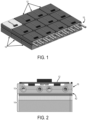
FIG. 1 shows an example of a liquid cooling assembly, in accordance with some embodiments described in the present disclosure, arranged between an array of printed circuit boards ("PCBs") and photodetector assemblies that collectively form a tiled array of radiation detectors. -
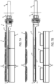
FIG. 2 shows a cross section through the tiled array of radiation detectors shown inFIG. 1 . -
FIG. 3 shows an example of a liquid cooling assembly in accordance with some embodiments described in the present disclosure. -
FIG. 4A shows a cross sectional view of an embodiment of a liquid cooling assembly as described in the present disclosure. -
FIG. 4B shows an exploded cross sectional view of another embodiment of a liquid cooling assembly described in the present disclosure. -
FIG. 5 shows a cross sectional view of another embodiment of a liquid cooling assembly as described in the present disclosure. -
FIG. 6 shows a schematic representation of an example arrangement of tubes, and their inflow and outflow, for use in a liquid cooling assembly, relative to photodetector assemblies of tileable radiation detectors. -
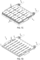
FIG. 7A shows a side view of an example tiled radiation detector array using a liquid cooling assembly in accordance with some embodiments described in the present disclosure. -
FIG. 7B shows an exploded side view of the example tiled radiation detector array shown inFIG. 7A . -
FIG. 7C shows another view of the example tiled radiation detector array show inFIG. 7A . -
FIG. 7D shows a view of the liquid cooling assembly used in the example tiled radiation detector array shown inFIG. 7A . -
FIG. 8 shows another embodiment of a liquid cooling assembly described in the present disclosure. - Described here are systems and methods for temperature controlled radiation detectors, such as liquid-cooled positron emission tomography ("PET") detectors. Particularly, temperature control is provided by a temperature control assembly that may include a liquid cooling assembly having a cold plate having formed therein one or more channels through which a liquid coolant is able to flow. The one or more channels are enclosed by the cold plate, such that the liquid coolant does not come into contact with sensitive electronic components used in the radiation detectors. Heating elements are provided to the cold plate of the liquid cooling assembly, which can be controlled to provide an additional level of temperature control. The precision of temperature control provided by the heating elements enables the maintenance of temperature for optimal performance of the radiation detector and associated electronics.
- As shown in
FIGS. 1 and 2 , the temperature control, which may include liquid cooling, is provided by aliquid cooling assembly 10 that is designed to be removably positioned between a printed circuit board ("PCB") 12 and aphotodetector assembly 14 of a tileable block detector. An example of tileable block detectors is described in co-pending PCT Application No.PCT/CA2017/050228 - As shown in
FIGS. 3, 4A, and 4B , theliquid cooling assembly 10 generally includes acold plate 16 having formed therein one ormore channels 18 into which one ormore tubes 20 are arranged. A liquid is provided to circulate through the one ormore tubes 20 orchannels 18 to remove heat that is transferred to thecold plate 16 from components on thePCB 12, thephotodetector assembly 14, or both. In some embodiments, notubes 20 are arranged in thechannels 18, and instead the liquid is provided directly to thechannels 18.FIG. 4A shows a cross section of an examplecold plate 16 in which notubes 20 are arranged in thechannels 18, andFIG. 4B shows an exploded cross section of an examplecold plate 16 in whichtubes 20 are arranged in thechannels 18. - The
cold plate 16 has afirst contact surface 22 that is placed into contact with thePCB 12, and asecond contact surface 24 that is opposite thefirst contact surface 22 and which is placed into contact with thephotodetector assembly 14. In some embodiments, thefirst contact surface 22 may directly contact thePCB 12, but in some other embodiments one or more layers (e.g., insulating or conductive layers) may be provided between thefirst contact surface 22 and thePCB 12. - A
recess 26 is formed on thefirst contact surface 22 side of thecold plate 16, such that components on thePCB 12 are allowed to extend into therecessed region 26 when thePCB 12 is coupled to thefirst contact surface 22 of thecold plate 16. - One or
more apertures 28 are formed in thecold plate 16 extending from thesecond contact surface 24 through to the surface in therecessed region 26. Theapertures 28 allow for electrical connectors to pass between thePCB 12 and thephotodetector assembly 14. For instance, thephotodetector assembly 14 can include a circuit board on which sensors or other data acquisition components are located, and electrical connectors can extend through theapertures 28 to electrically connect the sensor circuit boards with preamp circuit components located on thePCB 12. This construction allows the overall thickness of thecold plate 16 to be reduced. As one example, the thickness of thecold plate 16 can be up to 9.6 mm. - In some embodiments, the
cold plate 16 includes anupper plate 30 and alower plate 32 that is opposite theupper plate 30. As shown inFIG. 4B , theupper plate 30 includes an outward facing surface, which corresponds to thefirst contact surface 22 of thecold plate 16, and an inward facingsurface 34 that is opposite thefirst contact surface 22. Likewise, thelower plate 32 includes an outward facing surface that corresponds to thesecond contact surface 24 of thecold plate 16, as well as an inward facingsurface 36 that is opposite thesecond contact surface 24. In these instances, the inward facingsurface 34 of theupper plate 30 has formed thereinupper channel portions 38 and the inward facingsurface 36 of thelower plate 32 has matchinglower channel portions 40 formed therein. When the inward facingsurface 34 of theupper plate 30 is brought into contact with the inward facingsurface 36 of thelower plate 32, theupper channel portions 38 and thelower channel portions 40 meet to form the plurality ofchannels 18. As mentioned above, in some embodiments, one ormore tubes 20 are arranged in the plurality of channels and thus can be disposed between theupper plate 30 and thelower plate 32. - As shown in
FIG. 4B , the outward facing surface of thelower plate 32, which corresponds to thesecond contact surface 24 of thecold plate 16, has coupled thereto a thermallyconductive pad 42 that can be composed of a compressible material, such that mismatches between thecold plate 16 and the faces of thePCB 12 andphotodetector assembly 14 can be taken up, thereby increasing the contact surface of thecold plate 16. Preferably, the thermallyconductive pad 42 is composed of a material that is electrically insulating (i.e., has a relatively high dielectric constant). As one non-limiting example, the electrically insulating material can be a silicone elastomer. As another non-limiting example, the electrically insulating material can be a polyimide. The thermallyconductive pad 42 can be coupled to thesecond contact surface 24 using an adhesive, and may have formed therein apertures similar to theapertures 28 formed in thecold plate 16. - One or
more heating elements 60 are coupled to thefirst contact surface 22, thesecond contact surface 24, or both. As one example, theheating elements 60 can be coupled to thesecond contact surface 24 via coupling to the thermallyconductive pad 42. As an example, the one ormore heating elements 60 can include a thin film heating pad. The thin film heating pad can be constructed as an etched foil, which may be embedded in a substrate material, such as silicon or Kapton wrap, to provide electrical insulation. The one ormore heating elements 60 can be controlled via a controller in order to precisely control the temperature of the radiation detector assembly or its associated electrical components. - As an example, under high load of radiation, more heat will be generated by preamplifiers, therefore resulting in more powerful cooling. In these instances, the temperature of the sensors in the radiation detector assembly may change significantly, which is undesirable because such sensors are often highly sensitive to changes in temperature. The one or
more heating elements 60 can then be operated to increase the temperature of the radiation detector assembly, or its associated electrical components, to avoid overcooling and to maintain the radiation detector assembly operating within a temperature range in which the sensors have optimal or otherwise satisfactory performance. A temperature sensor is provided and coupled to theliquid cooling assembly 10 in order to monitor temperature. Feedback from the temperature sensor can then be used to control the operation of theheating elements 60 to precisely adjust the temperature of the radiation detector assembly in those instances where the radiation detector assembly may be overcooled by the liquid cooling assembly. For instance, power to theheating elements 60 can be controlled such that theheating elements 60 start heating only when the temperature of the sensors in the radiation detector assembly is changing. - The
upper plate 30 and thelower plate 32 can be composed of the same material, or in some instances can be composed of different materials. As one example, theupper plate 30 and thelower plate 32 can both be composed of copper or other thermally conductive metals, metal alloys, plastics, carbon fiber, carbon fiber epoxies, or other materials. - In some embodiments, the
cold plate 16 includes a single piece in which the one ormore channels 18 are machined or otherwise formed, as shown inFIG. 5 . In these instances, thecold plate 16 has afirst contact surface 22 that is placed into contact with thePCB 12, and asecond contact surface 24 opposite thefirst contact surface 22, which is placed into contact with thephotodetector assembly 14. A thermallyconductive pad 42 may also be coupled to thesecond contact surface 24, as noted above. - The
cold plate 16 can be dimensioned to provide thermal control (e.g., cooling, heating, or both) to a single tileable radiation detector, a large area monolithic radiation detector, or multiple tileable radiation detectors that are arranged in an array. For instance, thecold plate 16 can be dimensioned to provide cooling to an M × N array of tileable radiation detectors. In other instances, thecold plate 16 can be dimensioned to provide cooling to an M × 1 or 1 × N array of tileable radiation detectors. In these latter configurations, multiplecold plates 16 can be arrayed to provide cooling to larger array of tileable radiation detectors. These configurations have an advantage that if there is a failure in one of thecold plates 16 that particularcold pate 16 can be removed from theliquid cooling assembly 10 and replaced with a properly functioningcold plate 16 without having to replace the entire liquid cooling assembly. - As shown in
FIG. 3 , in some embodiments, eachtube 20 has aninlet 44 and anoutlet 46. In other embodiments, eachchannel 18 may have more than one inlet, more than one outlet, or combinations thereof. In those embodiments where atube 20 is not arranged in thechannel 18, then theinlet 44 andoutlet 46 are formed in thechannel 18 instead of thetube 20. - In some embodiments, the
channels 18,tube 20, or both, are constructed to form separate loops to maximize temperature uniformity, as shown inFIG. 6 . In such instances, eachchannel 18,tube 20, or both can be U-shaped, or can have other shapes and configurations. For ease of use, theinlet 44 andoutlet 46 can be arranged on the same side of thecold plate 16, but in other configurations theinlet 44 andoutlet 46 can be arranged on different sides of thecold plate 16. - A separate line can be provided to each
inlet 44 to provide inflow of a liquid into thechannels 18, and a separate line can be provided to eachoutlet 46 to provide outflow of the liquid from thechannels 18. In some embodiments, a manifold can be provided to connect eachinlet 44 together to a common inflow line and to connect eachoutlet 46 together to a common outflow line. The manifold can include a single structure that keeps theinlet 44 lines andoutlet 46 lines separate, or can include two separate structures, one for theinlet 44 lines and one for theoutlet 46 lines. -
FIGS. 7A-7D show an example in which aliquid cooling assembly 10 is arranged between an array ofPCBs 12 andphotodetector assemblies 14 corresponding to an array of tileable radiation detectors. In this example, liquid coolant is provided to the liquid cooling assembly via aninflow line 48. As the liquid coolant passes through thetubes 20 in theliquid cooling assembly 10 it removes heat from thePCBs 12 andphotodetector assemblies 14. The liquid coolant then leaves the liquid cooling assembly via anoutflow line 50, after which the liquid coolant can be cooled again for later use, recycled, or otherwise stored. - Preferably, the
inflow line 48 and theoutflow line 50 are composed of a flexible material, such as a flexible PVC. In these instances, the radiation detector (e.g., a tileable block detector composed ofPCBs 12 and photodetector assemblies 14) can be moved without needing to disconnect thecold plate 16. Such functionality is advantageous for medical procedures, such as those where it may be desired to perform a biopsy during which the radiation detector assembly needs to be moved to provide access to the patient. Such functionality can also be advantageous for multimodality imaging applications where it may be necessary to move the radiation detector assembly to provide access for other imaging modalities, such as x-ray or ultrasound imaging. As shown, light-tightflexible shrouds 56 can be coupled to theinflow line 48 and theoutflow line 50 in order to enable flexible tubing connection while maintaining light tightness for detector operation. As one example, the light-tightflexible shrouds 56 can be composed of silicone. - As seen in
FIG. 7B , thephotodetector assemblies 14 include anelectrical connector 52 that extends through theapertures 28 formed in thecold plate 16 in order to engage and electrically connect to thePCBs 12, as mentioned above. - In this example, the
cold plate 16 does not have arecess 26 formed in thefirst contact surface 22 side. In some embodiments, it will be appreciated that theapertures 28 can be sized and arranged such that some or all of the components on thePCBs 12 facing thefirst contact surface 22 extend into theapertures 28 when thePCBs 12 are coupled to thecold plate 16. - As seen in
FIGS. 7B and7D , an electrically insulatinglayer 54 can be coupled to thefirst contact surface 22 of thecold plate 16. As one example, the electrically insulating later 54 can be composed of a continuous-woven glass fabric laminate with an epoxy resin, such as FR4 Garolite® (McMaster-Carr), or other epoxy sheets or plastic sheets or laminates or carbon fiber compositions. The electrically insulatinglayer 54 can also reduce the thermal conductivity
FIG. 8 illustrates another example of aliquid cooling assembly 10 in which thecold plate 16 is composed of a bonded aluminum assembly, lid, and main body. Thecold plate 16 has an anodized finish, with contact face machined to expose metal. A compressible thermal pad can be coupled to the contact face. Theliquid cooling assembly 10 shown inFIG. 8 is sized to fit between a preamp PCBs and a sensor PCBs of photodetector assemblies. Theliquid cooling assembly 10 shown inFIG. 8 provides single path cooling with one port in and one port out. - The present disclosure has described one or more preferred embodiments, and it should be appreciated that many equivalents, alternatives, variations, and modifications, aside from those expressly stated, are possible and within the scope of the invention.
Claims (15)
- A temperature control assembly, comprising:a cold plate having a first contact surface and a second contact surface opposite the first contact surface, wherein the cold plate is composed of a thermally conductive material;a channel formed in the cold plate and enclosed by the cold plate between the first contact surface and the second contact surface of the cold plate;an inlet formed in the channel for providing inflow of a liquid to the channel;an outlet formed in the channel for providing outflow of the liquid from the channel;at least one aperture formed in the cold plate, wherein the aperture is sized to receive an electrical connection between a printed circuit board when the printed circuit board is coupled to the first contact surface of the cold plate and a photodetector assembly when the photodetector assembly is coupled to the second contact surface of the cold plate; andcharacterized in that the temperature control assembly further comprises:a thermally conductive pad coupled to the second contact surface;a heating element coupled to the thermally conductive pad; anda temperature sensor that measures a temperature of electrical components mounted to a printed circuit board when the printed circuit board is coupled to one of the first contact surface or the second contact surface, and wherein the temperature sensor provides the measured temperature to a controller in order to control a power supplied to the heating element.
- The temperature control assembly as recited in claim 1, further comprising a recess formed in the first contact surface of the cold plate and sized to receive electrical components mounted to a printed circuit board when the printed circuit board is coupled to the first contact surface of the cold plate.
- The temperature control assembly as recited in claim 1, further comprising a tube arranged in the channel, wherein the tube is composed of a thermally conductive material.
- The temperature control assembly as recited in claim 1, wherein the cold plate comprises an upper plate in contact with a lower plate, the upper plate having an outward facing surface corresponding to the first contact surface and an inward facing surface opposite the outward facing surface, and the lower plate having an outward facing surface corresponding to the second contact surface and an inward facing surface opposite the outward facing surface, wherein the inward facing surface of the upper plate is in contact with the inward facing surface of the lower plate.
- The temperature control assembly as recited in claim 4, wherein an upper channel portion is formed in the inward facing surface of the upper plate and a lower channel portion is formed in the inward facing surface of the lower plate, such that when the inward facing surface of the upper plate is in contact with the inward facing surface of the lower plate then upper channel portion and the lower channel portion form the channel.
- The temperature control assembly as recited in claim 4, wherein the upper plate is composed of a first conductive material and the lower plate is composed of a second conductive material that is different from the first conductive material
- The temperature control assembly as recited in claim 1, wherein the cold plate is composed of copper.
- The temperature control assembly as recited in claim 1, wherein the thermally conductive pad is composed of a compressible material.
- The temperature control assembly as recited in claim 1, wherein the heating element comprises a thin film heating element.
- The temperature control assembly as recited in claim 9, wherein the thin film comprises an etched foil.
- The temperature control assembly as recited in claim 1, wherein the heating element is coupled to the thermally conductive pad via a layer of thermally conductive material.
- The temperature control assembly as recited in claim 1, further comprising an electrically insulating layer arranged on the first contact surface.
- The temperature control assembly as recited in claim 12, wherein the electrically insulating layer is composed of an FR4 glass epoxy laminate.
- The temperature control assembly as recited in claim 1, wherein the channel comprises a plurality of channels, and each of the plurality of channel has a corresponding inlet and outlet formed therein.
- The temperature control assembly as recited in claim 14, wherein a tube is arranged in each of the plurality of channel, and wherein each tube is composed of a thermally conductive material.
Applications Claiming Priority (2)
| Application Number | Priority Date | Filing Date | Title |
|---|---|---|---|
| US201862722490P | 2018-08-24 | 2018-08-24 | |
| PCT/CA2019/051164 WO2020037430A1 (en) | 2018-08-24 | 2019-08-23 | Liquid cooling system for precise temperature control of radiation detector for positron emission mammography |
Publications (3)
| Publication Number | Publication Date |
|---|---|
| EP3841405A1 EP3841405A1 (en) | 2021-06-30 |
| EP3841405A4 EP3841405A4 (en) | 2022-05-04 |
| EP3841405B1 true EP3841405B1 (en) | 2025-01-29 |
Family
ID=69591059
Family Applications (1)
| Application Number | Title | Priority Date | Filing Date |
|---|---|---|---|
| EP19851236.0A Active EP3841405B1 (en) | 2018-08-24 | 2019-08-23 | Liquid cooling system for precise temperature control of radiation detector for positron emission mammography |
Country Status (5)
| Country | Link |
|---|---|
| US (1) | US12262463B2 (en) |
| EP (1) | EP3841405B1 (en) |
| CN (1) | CN113454490A (en) |
| CA (1) | CA3110407A1 (en) |
| WO (1) | WO2020037430A1 (en) |
Families Citing this family (2)
| Publication number | Priority date | Publication date | Assignee | Title |
|---|---|---|---|---|
| CN111236562B (en) * | 2020-03-09 | 2021-05-25 | 深圳市嘉信装饰设计工程有限公司 | An environmentally friendly and energy-saving interior decoration new material board |
| US12419010B2 (en) * | 2023-10-18 | 2025-09-16 | Ciena Corporation | Dual flow low profile coolant distribution manifold |
Family Cites Families (35)
| Publication number | Priority date | Publication date | Assignee | Title |
|---|---|---|---|---|
| US4245479A (en) * | 1978-01-19 | 1981-01-20 | Texaco Inc. | Temperature stabilization method |
| JPS56140274A (en) * | 1980-04-02 | 1981-11-02 | Nippon Steel Corp | Method and device for analysis of radon |
| US5610968A (en) * | 1995-03-17 | 1997-03-11 | Picker International, Inc. | High capacity cooling system for CT gantry |
| US6221045B1 (en) * | 1995-04-20 | 2001-04-24 | Acist Medical Systems, Inc. | Angiographic injector system with automatic high/low pressure switching |
| US6127663A (en) * | 1998-10-09 | 2000-10-03 | Ericsson Inc. | Electronics cabinet cooling system |
| EP1142001B1 (en) | 1998-11-20 | 2007-10-03 | Steag RTP Systems, Inc. | Fast heating and cooling apparatus for semiconductor wafers |
| JP4564141B2 (en) * | 2000-07-25 | 2010-10-20 | 株式会社東芝 | X-ray CT system |
| EP1396228A4 (en) * | 2001-06-07 | 2005-08-10 | Hitachi Medical Corp | X-ray diagnostic apparatus |
| US6711017B2 (en) * | 2001-07-17 | 2004-03-23 | Hitachi Kokusai Electric Inc. | Cooling apparatus for electronic unit |
| US6621071B2 (en) * | 2001-09-07 | 2003-09-16 | Raytheon Co. | Microelectronic system with integral cryocooler, and its fabrication and use |
| US20040022351A1 (en) * | 2002-07-30 | 2004-02-05 | Ge Medical Systems Global Technology Company, Llc | Thermoelectrically controlled x-ray detector array |
| DE10352382A1 (en) * | 2003-11-10 | 2005-06-23 | Siemens Ag | Method and control device for controlling the temperature of a detector system within a computer tomography device |
| JP4811552B2 (en) * | 2004-03-30 | 2011-11-09 | 独立行政法人科学技術振興機構 | Neutron detector using superconducting elements |
| CN100499089C (en) * | 2005-06-08 | 2009-06-10 | 富准精密工业(深圳)有限公司 | heat sink |
| JP2008267623A (en) * | 2007-04-17 | 2008-11-06 | Nikkeikin Aluminium Core Technology Co Ltd | Manufacturing method of heat exchanger, formation member and heat exchanger |
| JP5082610B2 (en) * | 2007-06-12 | 2012-11-28 | 日本軽金属株式会社 | Heat exchanger manufacturing method and heat exchanger |
| US8668560B2 (en) * | 2007-09-27 | 2014-03-11 | Dresser, Inc. | Shielding electronic components from liquid |
| JP5194862B2 (en) * | 2008-02-12 | 2013-05-08 | 株式会社島津製作所 | 2D image detector |
| KR100870578B1 (en) * | 2008-04-17 | 2008-11-27 | 주식회사 오스테오시스 | Radiation detector with excellent cooling and anti-frosting effect of semiconductor sensor |
| WO2010039946A2 (en) * | 2008-10-03 | 2010-04-08 | Cts Corporation | Ovenized crystal oscillator assembly |
| JP5424975B2 (en) * | 2010-04-27 | 2014-02-26 | 富士フイルム株式会社 | Storage case, device system |
| JP5595804B2 (en) * | 2010-06-21 | 2014-09-24 | 株式会社東芝 | X-ray CT system |
| US8590331B2 (en) * | 2010-10-13 | 2013-11-26 | Siemens Medical Solutions Usa, Inc. | Cooling unit for cooling a detection device in an imaging system and detection devices and imaging systems therefrom |
| US20120175094A1 (en) * | 2011-01-10 | 2012-07-12 | Asetek A/S | Liquid Cooling System Cold Plate Assembly |
| US20130037251A1 (en) * | 2011-08-11 | 2013-02-14 | General Electric Company | Liquid cooled thermal control system and method for cooling an imaging detector |
| WO2013111511A1 (en) * | 2012-01-23 | 2013-08-01 | 日本碍子株式会社 | Drying method and coating film drying furnace for coating film formed on pet film surface |
| US8938880B2 (en) * | 2012-02-20 | 2015-01-27 | Wolverine Tube, Inc. | Method of manufacturing an integrated cold plate for electronics |
| US20130284936A1 (en) * | 2012-04-30 | 2013-10-31 | General Electric Company | Positron emission tomogrpahy detector for dual-modality imaging |
| AU2013203000B9 (en) * | 2012-08-10 | 2017-02-02 | Lantheus Medical Imaging, Inc. | Compositions, methods, and systems for the synthesis and use of imaging agents |
| WO2014058501A1 (en) * | 2012-10-11 | 2014-04-17 | Laird Technologies, Inc. | Systems and methods for cooling x-ray tubes and detectors |
| US9364187B2 (en) * | 2014-05-03 | 2016-06-14 | General Electric Company | Packaging design for CT detector |
| JP6618984B2 (en) * | 2014-07-08 | 2019-12-11 | ワトロー エレクトリック マニュファクチュアリング カンパニー | Bonding assembly with integrated temperature sensing at the bond layer |
| EP3195711A4 (en) * | 2014-09-15 | 2018-08-29 | D'Onofrio, Nicholas, Michael | Liquid cooled metal core printed circuit board |
| US10001569B2 (en) * | 2015-08-31 | 2018-06-19 | General Electric Company | Positron emission tomography detector assembly for dual-modality imaging |
| US10178976B2 (en) * | 2016-01-29 | 2019-01-15 | Shanghai United Imaging Healthcare Co., Ltd. | Method and apparatus for temperature control in a PET detector |
-
2019
- 2019-08-23 US US17/270,611 patent/US12262463B2/en active Active
- 2019-08-23 WO PCT/CA2019/051164 patent/WO2020037430A1/en not_active Ceased
- 2019-08-23 CA CA3110407A patent/CA3110407A1/en active Pending
- 2019-08-23 EP EP19851236.0A patent/EP3841405B1/en active Active
- 2019-08-23 CN CN201980069553.3A patent/CN113454490A/en active Pending
Also Published As
| Publication number | Publication date |
|---|---|
| CA3110407A1 (en) | 2020-02-27 |
| EP3841405A1 (en) | 2021-06-30 |
| US20210337650A1 (en) | 2021-10-28 |
| US12262463B2 (en) | 2025-03-25 |
| WO2020037430A1 (en) | 2020-02-27 |
| EP3841405A4 (en) | 2022-05-04 |
| CN113454490A (en) | 2021-09-28 |
Similar Documents
| Publication | Publication Date | Title |
|---|---|---|
| CN106880373B (en) | PET imaging apparatus and PET-CT imaging apparatus | |
| JP3061292U (en) | Ultrasonic transducer structure | |
| EP4041463B1 (en) | Systems and methods for cooling ultrasound transducers and ultrasound transducer arrays | |
| EP1827070B1 (en) | Thermal management of electronic devices | |
| EP3647902B1 (en) | Liquid-cooled integrated circuit system | |
| US11540814B2 (en) | Systems, methods, and apparatuses for active thermal management of ultrasound transducers | |
| CN100506159C (en) | System and method for thermal management of ct detector circuitry | |
| US12262463B2 (en) | Liquid cooling system for precise temperature control of radiation detector for positron emission mammography | |
| CA2960200A1 (en) | Thermal management methods and apparatus | |
| EP2294496A2 (en) | Graphics card thermal interposer | |
| US9151814B2 (en) | Power electronics assembly for a magnetic resonance device | |
| JP2003067087A (en) | Liquid cooling system for portable information processing equipment | |
| CN107209538A (en) | Liquid cooling with cooling chamber | |
| JP2023017788A (en) | Immersion cooling temperature control method, system, and apparatus | |
| WO2022241078A1 (en) | Power supply for a mining machine | |
| CN104428891B (en) | Integrated electronics module with cooling structure | |
| CN113271748A (en) | Electronic device | |
| JP4807121B2 (en) | Radiation detector | |
| EP4434471B1 (en) | Heat-dissipating arrangements for medical devices and associated devices, and systems | |
| CN212006296U (en) | TEC heat dissipation assembly for direct-insertion type multi-element area array detector | |
| JP2005207906A (en) | Radiation detector and radiation imaging apparatus | |
| JP4991633B2 (en) | Cooling system for electronic equipment | |
| WO2025183687A1 (en) | Cooling system for medical imaging apparatus | |
| WO2022245809A1 (en) | A passive heat dissipation power supply for it equipment | |
| JP2017227540A (en) | Radiation image imaging device |
Legal Events
| Date | Code | Title | Description |
|---|---|---|---|
| STAA | Information on the status of an ep patent application or granted ep patent |
Free format text: STATUS: THE INTERNATIONAL PUBLICATION HAS BEEN MADE |
|
| PUAI | Public reference made under article 153(3) epc to a published international application that has entered the european phase |
Free format text: ORIGINAL CODE: 0009012 |
|
| STAA | Information on the status of an ep patent application or granted ep patent |
Free format text: STATUS: REQUEST FOR EXAMINATION WAS MADE |
|
| 17P | Request for examination filed |
Effective date: 20210322 |
|
| AK | Designated contracting states |
Kind code of ref document: A1 Designated state(s): AL AT BE BG CH CY CZ DE DK EE ES FI FR GB GR HR HU IE IS IT LI LT LU LV MC MK MT NL NO PL PT RO RS SE SI SK SM TR |
|
| DAV | Request for validation of the european patent (deleted) | ||
| DAX | Request for extension of the european patent (deleted) | ||
| A4 | Supplementary search report drawn up and despatched |
Effective date: 20220330 |
|
| RIC1 | Information provided on ipc code assigned before grant |
Ipc: G01T 1/29 20060101ALI20220325BHEP Ipc: A61B 6/00 20060101ALI20220325BHEP Ipc: A61B 6/03 20060101ALI20220325BHEP Ipc: G01J 1/02 20060101ALI20220325BHEP Ipc: G01T 7/00 20060101AFI20220325BHEP |
|
| RIN1 | Information on inventor provided before grant (corrected) |
Inventor name: GILLESPIE, CHRISTOPHER Inventor name: REZNIK, ALLA Inventor name: BUBON, OLEKSANDR |
|
| REG | Reference to a national code |
Ref country code: DE Ref legal event code: R079 Free format text: PREVIOUS MAIN CLASS: G01T0007000000 Ipc: A61B0006500000 Ref document number: 602019065483 Country of ref document: DE |
|
| GRAP | Despatch of communication of intention to grant a patent |
Free format text: ORIGINAL CODE: EPIDOSNIGR1 |
|
| STAA | Information on the status of an ep patent application or granted ep patent |
Free format text: STATUS: GRANT OF PATENT IS INTENDED |
|
| RIC1 | Information provided on ipc code assigned before grant |
Ipc: A61B 6/00 20060101ALI20240731BHEP Ipc: A61B 6/03 20060101ALI20240731BHEP Ipc: G01T 1/29 20060101ALI20240731BHEP Ipc: A61B 6/50 20240101AFI20240731BHEP |
|
| INTG | Intention to grant announced |
Effective date: 20240821 |
|
| GRAS | Grant fee paid |
Free format text: ORIGINAL CODE: EPIDOSNIGR3 |
|
| GRAA | (expected) grant |
Free format text: ORIGINAL CODE: 0009210 |
|
| STAA | Information on the status of an ep patent application or granted ep patent |
Free format text: STATUS: THE PATENT HAS BEEN GRANTED |
|
| AK | Designated contracting states |
Kind code of ref document: B1 Designated state(s): AL AT BE BG CH CY CZ DE DK EE ES FI FR GB GR HR HU IE IS IT LI LT LU LV MC MK MT NL NO PL PT RO RS SE SI SK SM TR |
|
| REG | Reference to a national code |
Ref country code: GB Ref legal event code: FG4D |
|
| REG | Reference to a national code |
Ref country code: CH Ref legal event code: EP |
|
| REG | Reference to a national code |
Ref country code: DE Ref legal event code: R096 Ref document number: 602019065483 Country of ref document: DE |
|
| REG | Reference to a national code |
Ref country code: IE Ref legal event code: FG4D |
|
| REG | Reference to a national code |
Ref country code: NL Ref legal event code: MP Effective date: 20250129 |
|
| PG25 | Lapsed in a contracting state [announced via postgrant information from national office to epo] |
Ref country code: NL Free format text: LAPSE BECAUSE OF FAILURE TO SUBMIT A TRANSLATION OF THE DESCRIPTION OR TO PAY THE FEE WITHIN THE PRESCRIBED TIME-LIMIT Effective date: 20250129 |
|
| PG25 | Lapsed in a contracting state [announced via postgrant information from national office to epo] |
Ref country code: RS Free format text: LAPSE BECAUSE OF FAILURE TO SUBMIT A TRANSLATION OF THE DESCRIPTION OR TO PAY THE FEE WITHIN THE PRESCRIBED TIME-LIMIT Effective date: 20250429 |
|
| PG25 | Lapsed in a contracting state [announced via postgrant information from national office to epo] |
Ref country code: FI Free format text: LAPSE BECAUSE OF FAILURE TO SUBMIT A TRANSLATION OF THE DESCRIPTION OR TO PAY THE FEE WITHIN THE PRESCRIBED TIME-LIMIT Effective date: 20250129 |
|
| PG25 | Lapsed in a contracting state [announced via postgrant information from national office to epo] |
Ref country code: PL Free format text: LAPSE BECAUSE OF FAILURE TO SUBMIT A TRANSLATION OF THE DESCRIPTION OR TO PAY THE FEE WITHIN THE PRESCRIBED TIME-LIMIT Effective date: 20250129 |
|
| PG25 | Lapsed in a contracting state [announced via postgrant information from national office to epo] |
Ref country code: ES Free format text: LAPSE BECAUSE OF FAILURE TO SUBMIT A TRANSLATION OF THE DESCRIPTION OR TO PAY THE FEE WITHIN THE PRESCRIBED TIME-LIMIT Effective date: 20250129 |
|
| REG | Reference to a national code |
Ref country code: LT Ref legal event code: MG9D |
|
| PG25 | Lapsed in a contracting state [announced via postgrant information from national office to epo] |
Ref country code: NO Free format text: LAPSE BECAUSE OF FAILURE TO SUBMIT A TRANSLATION OF THE DESCRIPTION OR TO PAY THE FEE WITHIN THE PRESCRIBED TIME-LIMIT Effective date: 20250429 Ref country code: IS Free format text: LAPSE BECAUSE OF FAILURE TO SUBMIT A TRANSLATION OF THE DESCRIPTION OR TO PAY THE FEE WITHIN THE PRESCRIBED TIME-LIMIT Effective date: 20250529 |
|
| REG | Reference to a national code |
Ref country code: AT Ref legal event code: MK05 Ref document number: 1762654 Country of ref document: AT Kind code of ref document: T Effective date: 20250129 |
|
| PG25 | Lapsed in a contracting state [announced via postgrant information from national office to epo] |
Ref country code: HR Free format text: LAPSE BECAUSE OF FAILURE TO SUBMIT A TRANSLATION OF THE DESCRIPTION OR TO PAY THE FEE WITHIN THE PRESCRIBED TIME-LIMIT Effective date: 20250129 |
|
| PG25 | Lapsed in a contracting state [announced via postgrant information from national office to epo] |
Ref country code: LV Free format text: LAPSE BECAUSE OF FAILURE TO SUBMIT A TRANSLATION OF THE DESCRIPTION OR TO PAY THE FEE WITHIN THE PRESCRIBED TIME-LIMIT Effective date: 20250129 Ref country code: PT Free format text: LAPSE BECAUSE OF FAILURE TO SUBMIT A TRANSLATION OF THE DESCRIPTION OR TO PAY THE FEE WITHIN THE PRESCRIBED TIME-LIMIT Effective date: 20250529 |
|
| PG25 | Lapsed in a contracting state [announced via postgrant information from national office to epo] |
Ref country code: GR Free format text: LAPSE BECAUSE OF FAILURE TO SUBMIT A TRANSLATION OF THE DESCRIPTION OR TO PAY THE FEE WITHIN THE PRESCRIBED TIME-LIMIT Effective date: 20250430 Ref country code: BG Free format text: LAPSE BECAUSE OF FAILURE TO SUBMIT A TRANSLATION OF THE DESCRIPTION OR TO PAY THE FEE WITHIN THE PRESCRIBED TIME-LIMIT Effective date: 20250129 |
|
| PG25 | Lapsed in a contracting state [announced via postgrant information from national office to epo] |
Ref country code: AT Free format text: LAPSE BECAUSE OF FAILURE TO SUBMIT A TRANSLATION OF THE DESCRIPTION OR TO PAY THE FEE WITHIN THE PRESCRIBED TIME-LIMIT Effective date: 20250129 |
|
| PG25 | Lapsed in a contracting state [announced via postgrant information from national office to epo] |
Ref country code: SE Free format text: LAPSE BECAUSE OF FAILURE TO SUBMIT A TRANSLATION OF THE DESCRIPTION OR TO PAY THE FEE WITHIN THE PRESCRIBED TIME-LIMIT Effective date: 20250129 |
|
| PG25 | Lapsed in a contracting state [announced via postgrant information from national office to epo] |
Ref country code: SM Free format text: LAPSE BECAUSE OF FAILURE TO SUBMIT A TRANSLATION OF THE DESCRIPTION OR TO PAY THE FEE WITHIN THE PRESCRIBED TIME-LIMIT Effective date: 20250129 |
|
| PG25 | Lapsed in a contracting state [announced via postgrant information from national office to epo] |
Ref country code: DK Free format text: LAPSE BECAUSE OF FAILURE TO SUBMIT A TRANSLATION OF THE DESCRIPTION OR TO PAY THE FEE WITHIN THE PRESCRIBED TIME-LIMIT Effective date: 20250129 |
|
| PGFP | Annual fee paid to national office [announced via postgrant information from national office to epo] |
Ref country code: DE Payment date: 20250919 Year of fee payment: 7 |
|
| PG25 | Lapsed in a contracting state [announced via postgrant information from national office to epo] |
Ref country code: IT Free format text: LAPSE BECAUSE OF FAILURE TO SUBMIT A TRANSLATION OF THE DESCRIPTION OR TO PAY THE FEE WITHIN THE PRESCRIBED TIME-LIMIT Effective date: 20250129 |
|
| PGFP | Annual fee paid to national office [announced via postgrant information from national office to epo] |
Ref country code: GB Payment date: 20250923 Year of fee payment: 7 |
|
| PGFP | Annual fee paid to national office [announced via postgrant information from national office to epo] |
Ref country code: FR Payment date: 20250829 Year of fee payment: 7 |
|
| PG25 | Lapsed in a contracting state [announced via postgrant information from national office to epo] |
Ref country code: EE Free format text: LAPSE BECAUSE OF FAILURE TO SUBMIT A TRANSLATION OF THE DESCRIPTION OR TO PAY THE FEE WITHIN THE PRESCRIBED TIME-LIMIT Effective date: 20250129 Ref country code: CZ Free format text: LAPSE BECAUSE OF FAILURE TO SUBMIT A TRANSLATION OF THE DESCRIPTION OR TO PAY THE FEE WITHIN THE PRESCRIBED TIME-LIMIT Effective date: 20250129 |
|
| PG25 | Lapsed in a contracting state [announced via postgrant information from national office to epo] |
Ref country code: RO Free format text: LAPSE BECAUSE OF FAILURE TO SUBMIT A TRANSLATION OF THE DESCRIPTION OR TO PAY THE FEE WITHIN THE PRESCRIBED TIME-LIMIT Effective date: 20250129 |
|
| PG25 | Lapsed in a contracting state [announced via postgrant information from national office to epo] |
Ref country code: SK Free format text: LAPSE BECAUSE OF FAILURE TO SUBMIT A TRANSLATION OF THE DESCRIPTION OR TO PAY THE FEE WITHIN THE PRESCRIBED TIME-LIMIT Effective date: 20250129 |
|
| REG | Reference to a national code |
Ref country code: DE Ref legal event code: R097 Ref document number: 602019065483 Country of ref document: DE |
|
| PLBE | No opposition filed within time limit |
Free format text: ORIGINAL CODE: 0009261 |
|
| STAA | Information on the status of an ep patent application or granted ep patent |
Free format text: STATUS: NO OPPOSITION FILED WITHIN TIME LIMIT |
|
| REG | Reference to a national code |
Ref country code: CH Ref legal event code: L10 Free format text: ST27 STATUS EVENT CODE: U-0-0-L10-L00 (AS PROVIDED BY THE NATIONAL OFFICE) Effective date: 20251210 |
|
| 26N | No opposition filed |
Effective date: 20251030 |
|
| REG | Reference to a national code |
Ref country code: CH Ref legal event code: H13 Free format text: ST27 STATUS EVENT CODE: U-0-0-H10-H13 (AS PROVIDED BY THE NATIONAL OFFICE) Effective date: 20260324 |
|
| PG25 | Lapsed in a contracting state [announced via postgrant information from national office to epo] |
Ref country code: MC Free format text: LAPSE BECAUSE OF FAILURE TO SUBMIT A TRANSLATION OF THE DESCRIPTION OR TO PAY THE FEE WITHIN THE PRESCRIBED TIME-LIMIT Effective date: 20250129 |
|
| PG25 | Lapsed in a contracting state [announced via postgrant information from national office to epo] |
Ref country code: LU Free format text: LAPSE BECAUSE OF NON-PAYMENT OF DUE FEES Effective date: 20250823 |
|
| PG25 | Lapsed in a contracting state [announced via postgrant information from national office to epo] |
Ref country code: CH Free format text: LAPSE BECAUSE OF NON-PAYMENT OF DUE FEES Effective date: 20250831 |