EP3840054A1 - Self-aligned contacts for walled nanosheet and forksheet field effect transistor devices - Google Patents
Self-aligned contacts for walled nanosheet and forksheet field effect transistor devices Download PDFInfo
- Publication number
- EP3840054A1 EP3840054A1 EP19218708.6A EP19218708A EP3840054A1 EP 3840054 A1 EP3840054 A1 EP 3840054A1 EP 19218708 A EP19218708 A EP 19218708A EP 3840054 A1 EP3840054 A1 EP 3840054A1
- Authority
- EP
- European Patent Office
- Prior art keywords
- trench
- transistor structure
- transistor
- forming
- source
- Prior art date
- Legal status (The legal status is an assumption and is not a legal conclusion. Google has not performed a legal analysis and makes no representation as to the accuracy of the status listed.)
- Granted
Links
Images


Classifications
-
- H—ELECTRICITY
- H10—SEMICONDUCTOR DEVICES; ELECTRIC SOLID-STATE DEVICES NOT OTHERWISE PROVIDED FOR
- H10D—INORGANIC ELECTRIC SEMICONDUCTOR DEVICES
- H10D30/00—Field-effect transistors [FET]
- H10D30/01—Manufacture or treatment
- H10D30/021—Manufacture or treatment of FETs having insulated gates [IGFET]
- H10D30/0215—Manufacture or treatment of FETs having insulated gates [IGFET] using self-aligned selective metal deposition simultaneously on gate electrodes and the source regions or drain regions
-
- H—ELECTRICITY
- H10—SEMICONDUCTOR DEVICES; ELECTRIC SOLID-STATE DEVICES NOT OTHERWISE PROVIDED FOR
- H10D—INORGANIC ELECTRIC SEMICONDUCTOR DEVICES
- H10D30/00—Field-effect transistors [FET]
- H10D30/01—Manufacture or treatment
- H10D30/014—Manufacture or treatment of FETs having zero-dimensional [0D] or one-dimensional [1D] channels, e.g. quantum wire FETs, single-electron transistors [SET] or Coulomb blockade transistors
-
- H—ELECTRICITY
- H10—SEMICONDUCTOR DEVICES; ELECTRIC SOLID-STATE DEVICES NOT OTHERWISE PROVIDED FOR
- H10D—INORGANIC ELECTRIC SEMICONDUCTOR DEVICES
- H10D30/00—Field-effect transistors [FET]
- H10D30/01—Manufacture or treatment
- H10D30/021—Manufacture or treatment of FETs having insulated gates [IGFET]
- H10D30/031—Manufacture or treatment of FETs having insulated gates [IGFET] of thin-film transistors [TFT]
-
- H—ELECTRICITY
- H10—SEMICONDUCTOR DEVICES; ELECTRIC SOLID-STATE DEVICES NOT OTHERWISE PROVIDED FOR
- H10D—INORGANIC ELECTRIC SEMICONDUCTOR DEVICES
- H10D30/00—Field-effect transistors [FET]
- H10D30/40—FETs having zero-dimensional [0D], one-dimensional [1D] or two-dimensional [2D] charge carrier gas channels
- H10D30/43—FETs having zero-dimensional [0D], one-dimensional [1D] or two-dimensional [2D] charge carrier gas channels having one-dimensional [1D] charge carrier gas channels, e.g. quantum wire FETs or transistors having 1D quantum-confined channels
-
- H—ELECTRICITY
- H10—SEMICONDUCTOR DEVICES; ELECTRIC SOLID-STATE DEVICES NOT OTHERWISE PROVIDED FOR
- H10D—INORGANIC ELECTRIC SEMICONDUCTOR DEVICES
- H10D30/00—Field-effect transistors [FET]
- H10D30/60—Insulated-gate field-effect transistors [IGFET]
- H10D30/67—Thin-film transistors [TFT]
- H10D30/6729—Thin-film transistors [TFT] characterised by the electrodes
-
- H—ELECTRICITY
- H10—SEMICONDUCTOR DEVICES; ELECTRIC SOLID-STATE DEVICES NOT OTHERWISE PROVIDED FOR
- H10D—INORGANIC ELECTRIC SEMICONDUCTOR DEVICES
- H10D30/00—Field-effect transistors [FET]
- H10D30/60—Insulated-gate field-effect transistors [IGFET]
- H10D30/67—Thin-film transistors [TFT]
- H10D30/6729—Thin-film transistors [TFT] characterised by the electrodes
- H10D30/673—Thin-film transistors [TFT] characterised by the electrodes characterised by the shapes, relative sizes or dispositions of the gate electrodes
- H10D30/6735—Thin-film transistors [TFT] characterised by the electrodes characterised by the shapes, relative sizes or dispositions of the gate electrodes having gates fully surrounding the channels, e.g. gate-all-around
-
- H—ELECTRICITY
- H10—SEMICONDUCTOR DEVICES; ELECTRIC SOLID-STATE DEVICES NOT OTHERWISE PROVIDED FOR
- H10D—INORGANIC ELECTRIC SEMICONDUCTOR DEVICES
- H10D30/00—Field-effect transistors [FET]
- H10D30/60—Insulated-gate field-effect transistors [IGFET]
- H10D30/67—Thin-film transistors [TFT]
- H10D30/6757—Thin-film transistors [TFT] characterised by the structure of the channel, e.g. transverse or longitudinal shape or doping profile
-
- H—ELECTRICITY
- H10—SEMICONDUCTOR DEVICES; ELECTRIC SOLID-STATE DEVICES NOT OTHERWISE PROVIDED FOR
- H10D—INORGANIC ELECTRIC SEMICONDUCTOR DEVICES
- H10D62/00—Semiconductor bodies, or regions thereof, of devices having potential barriers
- H10D62/10—Shapes, relative sizes or dispositions of the regions of the semiconductor bodies; Shapes of the semiconductor bodies
- H10D62/113—Isolations within a component, i.e. internal isolations
- H10D62/115—Dielectric isolations, e.g. air gaps
- H10D62/116—Dielectric isolations, e.g. air gaps adjoining the input or output regions of field-effect devices, e.g. adjoining source or drain regions
-
- H—ELECTRICITY
- H10—SEMICONDUCTOR DEVICES; ELECTRIC SOLID-STATE DEVICES NOT OTHERWISE PROVIDED FOR
- H10D—INORGANIC ELECTRIC SEMICONDUCTOR DEVICES
- H10D62/00—Semiconductor bodies, or regions thereof, of devices having potential barriers
- H10D62/10—Shapes, relative sizes or dispositions of the regions of the semiconductor bodies; Shapes of the semiconductor bodies
- H10D62/117—Shapes of semiconductor bodies
- H10D62/118—Nanostructure semiconductor bodies
- H10D62/119—Nanowire, nanosheet or nanotube semiconductor bodies
- H10D62/121—Nanowire, nanosheet or nanotube semiconductor bodies oriented parallel to substrates
-
- H—ELECTRICITY
- H10—SEMICONDUCTOR DEVICES; ELECTRIC SOLID-STATE DEVICES NOT OTHERWISE PROVIDED FOR
- H10D—INORGANIC ELECTRIC SEMICONDUCTOR DEVICES
- H10D84/00—Integrated devices formed in or on semiconductor substrates that comprise only semiconducting layers, e.g. on Si wafers or on GaAs-on-Si wafers
- H10D84/01—Manufacture or treatment
- H10D84/0123—Integrating together multiple components covered by H10D12/00 or H10D30/00, e.g. integrating multiple IGBTs
- H10D84/0126—Integrating together multiple components covered by H10D12/00 or H10D30/00, e.g. integrating multiple IGBTs the components including insulated gates, e.g. IGFETs
- H10D84/0165—Integrating together multiple components covered by H10D12/00 or H10D30/00, e.g. integrating multiple IGBTs the components including insulated gates, e.g. IGFETs the components including complementary IGFETs, e.g. CMOS devices
- H10D84/0167—Manufacturing their channels
-
- H—ELECTRICITY
- H10—SEMICONDUCTOR DEVICES; ELECTRIC SOLID-STATE DEVICES NOT OTHERWISE PROVIDED FOR
- H10D—INORGANIC ELECTRIC SEMICONDUCTOR DEVICES
- H10D84/00—Integrated devices formed in or on semiconductor substrates that comprise only semiconducting layers, e.g. on Si wafers or on GaAs-on-Si wafers
- H10D84/01—Manufacture or treatment
- H10D84/0123—Integrating together multiple components covered by H10D12/00 or H10D30/00, e.g. integrating multiple IGBTs
- H10D84/0126—Integrating together multiple components covered by H10D12/00 or H10D30/00, e.g. integrating multiple IGBTs the components including insulated gates, e.g. IGFETs
- H10D84/0165—Integrating together multiple components covered by H10D12/00 or H10D30/00, e.g. integrating multiple IGBTs the components including insulated gates, e.g. IGFETs the components including complementary IGFETs, e.g. CMOS devices
- H10D84/0186—Manufacturing their interconnections or electrodes, e.g. source or drain electrodes
-
- H—ELECTRICITY
- H10—SEMICONDUCTOR DEVICES; ELECTRIC SOLID-STATE DEVICES NOT OTHERWISE PROVIDED FOR
- H10D—INORGANIC ELECTRIC SEMICONDUCTOR DEVICES
- H10D84/00—Integrated devices formed in or on semiconductor substrates that comprise only semiconducting layers, e.g. on Si wafers or on GaAs-on-Si wafers
- H10D84/01—Manufacture or treatment
- H10D84/02—Manufacture or treatment characterised by using material-based technologies
- H10D84/03—Manufacture or treatment characterised by using material-based technologies using Group IV technology, e.g. silicon technology or silicon-carbide [SiC] technology
- H10D84/038—Manufacture or treatment characterised by using material-based technologies using Group IV technology, e.g. silicon technology or silicon-carbide [SiC] technology using silicon technology, e.g. SiGe
-
- H—ELECTRICITY
- H10—SEMICONDUCTOR DEVICES; ELECTRIC SOLID-STATE DEVICES NOT OTHERWISE PROVIDED FOR
- H10D—INORGANIC ELECTRIC SEMICONDUCTOR DEVICES
- H10D84/00—Integrated devices formed in or on semiconductor substrates that comprise only semiconducting layers, e.g. on Si wafers or on GaAs-on-Si wafers
- H10D84/80—Integrated devices formed in or on semiconductor substrates that comprise only semiconducting layers, e.g. on Si wafers or on GaAs-on-Si wafers characterised by the integration of at least one component covered by groups H10D12/00 or H10D30/00, e.g. integration of IGFETs
- H10D84/82—Integrated devices formed in or on semiconductor substrates that comprise only semiconducting layers, e.g. on Si wafers or on GaAs-on-Si wafers characterised by the integration of at least one component covered by groups H10D12/00 or H10D30/00, e.g. integration of IGFETs of only field-effect components
- H10D84/83—Integrated devices formed in or on semiconductor substrates that comprise only semiconducting layers, e.g. on Si wafers or on GaAs-on-Si wafers characterised by the integration of at least one component covered by groups H10D12/00 or H10D30/00, e.g. integration of IGFETs of only field-effect components of only insulated-gate FETs [IGFET]
- H10D84/85—Complementary IGFETs, e.g. CMOS
-
- H—ELECTRICITY
- H10—SEMICONDUCTOR DEVICES; ELECTRIC SOLID-STATE DEVICES NOT OTHERWISE PROVIDED FOR
- H10P—GENERIC PROCESSES OR APPARATUS FOR THE MANUFACTURE OR TREATMENT OF DEVICES COVERED BY CLASS H10
- H10P14/00—Formation of materials, e.g. in the shape of layers or pillars
- H10P14/20—Formation of materials, e.g. in the shape of layers or pillars of semiconductor materials
- H10P14/34—Deposited materials, e.g. layers
- H10P14/3451—Structure
- H10P14/3452—Microstructure
- H10P14/3462—Nanowires
-
- H—ELECTRICITY
- H10—SEMICONDUCTOR DEVICES; ELECTRIC SOLID-STATE DEVICES NOT OTHERWISE PROVIDED FOR
- H10W—GENERIC PACKAGES, INTERCONNECTIONS, CONNECTORS OR OTHER CONSTRUCTIONAL DETAILS OF DEVICES COVERED BY CLASS H10
- H10W20/00—Interconnections in chips, wafers or substrates
- H10W20/01—Manufacture or treatment
- H10W20/021—Manufacture or treatment of interconnections within wafers or substrates
-
- H—ELECTRICITY
- H10—SEMICONDUCTOR DEVICES; ELECTRIC SOLID-STATE DEVICES NOT OTHERWISE PROVIDED FOR
- H10W—GENERIC PACKAGES, INTERCONNECTIONS, CONNECTORS OR OTHER CONSTRUCTIONAL DETAILS OF DEVICES COVERED BY CLASS H10
- H10W20/00—Interconnections in chips, wafers or substrates
- H10W20/01—Manufacture or treatment
- H10W20/031—Manufacture or treatment of conductive parts of the interconnections
- H10W20/069—Manufacture or treatment of conductive parts of the interconnections by forming self-aligned vias or self-aligned contact plugs
-
- H—ELECTRICITY
- H10—SEMICONDUCTOR DEVICES; ELECTRIC SOLID-STATE DEVICES NOT OTHERWISE PROVIDED FOR
- H10W—GENERIC PACKAGES, INTERCONNECTIONS, CONNECTORS OR OTHER CONSTRUCTIONAL DETAILS OF DEVICES COVERED BY CLASS H10
- H10W20/00—Interconnections in chips, wafers or substrates
- H10W20/01—Manufacture or treatment
- H10W20/031—Manufacture or treatment of conductive parts of the interconnections
- H10W20/0698—Local interconnections
-
- H—ELECTRICITY
- H10—SEMICONDUCTOR DEVICES; ELECTRIC SOLID-STATE DEVICES NOT OTHERWISE PROVIDED FOR
- H10W—GENERIC PACKAGES, INTERCONNECTIONS, CONNECTORS OR OTHER CONSTRUCTIONAL DETAILS OF DEVICES COVERED BY CLASS H10
- H10W20/00—Interconnections in chips, wafers or substrates
- H10W20/40—Interconnections external to wafers or substrates, e.g. back-end-of-line [BEOL] metallisations or vias connecting to gate electrodes
- H10W20/41—Interconnections external to wafers or substrates, e.g. back-end-of-line [BEOL] metallisations or vias connecting to gate electrodes characterised by their conductive parts
- H10W20/427—Power or ground buses
Definitions
- the present inventive concept relates to the field of forming semiconductor devices.
- Horizontal channel field effect transistor (FET) devices include the finFET, which has a gate straddling a channel portion of a fin-shaped semiconductor structure, and the horizontal nanowire- or nanosheet-FET (horizontal NWFET or NSFET), which has a gate at least partly enclosing a channel portion of a horizontally oriented nanowire- or nanosheet-shaped semiconductor structure.
- FET Horizontal channel field effect transistor
- An objective of the present disclosure is therefore to provide an improved method for forming a semiconductor structure including FET devices.
- a method for forming a semiconductor device comprising a first field-effect transistor, FET, device and a second FET device, the method comprising:
- transistor structure will refer to a semiconductor structure from which a transistor (or FET device) may be formed.
- transistor structures and thus, in the end, the final FET devices comprise a plurality of horizontally stacked nanosheets.
- Each of the transistor structures may form, or be arranged to subsequently form, a FET device.
- a channel FET device is hereby meant a device comprising a semiconductor structure comprising a first and a second source/drain portion and a channel portion located intermediate and extending between the first and second source/drain portions, and further comprising a gate structure extending along the channel portion.
- the first and second source/drain portions and the channel portion may intersect a common horizontal plane.
- the channel portion is adapted to (in use of the device) conduct a flow of charge carriers between the source/drain.
- the term “vertical” denotes a direction or orientation (e.g. of a surface, a dimension or other feature) parallel to a normal to the substrate (i.e. a main plane of extension or main/upper surface thereof).
- the term “horizontal” meanwhile denotes a direction or orientation parallel to the substrate (i.e. a main plane of extension or main surface thereof), or equivalently transverse to the vertical direction.
- terms such as “above”, “upper”, “top” and “below”, “lower”, “bottom” refer to relative positions as viewed along the vertical direction and does hence not imply an absolute orientation of the substrate or device.
- the contact material layer is divided into a first contact and a second contact separated by the first dielectric wall.
- the first contact is contacting the first source/drain region of the first transistor structure.
- the second contact is contacting the first source/drain portion of the second transistor structure.
- the first contact may wrap around at least two surfaces of the first source/drain portion of the first transistor structure, and the first contact may wrap around at least two surfaces of the first source/drain portion of the second transistor structure.
- the method may comprise depositing the contact material to form wrap-around contacts.
- a wrap-around contact may improve the control of the contact on the source/drain portion.
- the size and position of the contacts may be defined by the first dielectric wall.
- the contacts may thus be formed self-aligned with the first trench and the first source/drain portions.
- the distance between adjacent contacts is limited by the width of the first dielectric wall.
- the separation of the contacts may be controlled by the width of the first dielectric wall.
- the contacts may be formed with higher accuracy.
- the contacts may also be formed with a smaller pitch (distance) between them.
- the above-defined method may thus reduce the size of the resulting FET devices.
- the first FET device and the second FET device may be of the same dopant type.
- both the first FET device and the second FET device may be p-type FET devices.
- both the first FET device and the second FET device may be n-type FET devices.
- first FET device and the second FET device may also be of the opposite dopant type.
- depositing a contact material may comprise depositing said contact material in a continuous line extending in a direction from the first source direction from the first source/drain portion of the first transistor structure towards the first source/drain portion of the second transistor structure, across the transistor structures, the first trench and the first dielectric wall.
- the contact material may thus be deposited such that a continuous line is formed in the horizontal plane across from the first source/drain portion of the first transistor structure towards a first source/drain portion of the second transistor structure.
- Applying the contact material in a continuous line across (a source/drain region of) both transistor structures and then etching back the contact material below a top surface of the first dielectric wall to divide the contact material line into individual contacts may facilitate the formation of the contacts.
- Forming a continuous line of contact material and dividing it into individual contacts may for example be more convenient than applying the material as discrete contacts. Specifically, such a method may provide that smaller contacts may be formed with a higher accuracy.
- forming the dielectric wall may comprise forming spacers in the first trench at sidewalls of the first transistor structure and the second transistor structure.
- the spacers may protrude above a top surface of the transistor structures.
- Forming the first dielectric wall may further comprise forming the first dielectric wall in the first trench between the spacers and removing the spacers.
- the spacer material may be formed conformally in the trench, and then anisotropically (top-down) etched to form the spacers.
- the dielectric wall may be formed by filling a gap between the spacers with a dielectric material.
- the spacers may for example be removed using a selective etch.
- Forming spacers on the sidewalls of the first and second transistor structure and then forming the first dielectric wall between the spacers may provide that the dielectric wall is formed self-aligned between the transistor structures.
- forming the first transistor structure and the second transistor structure may comprise, prior to the formation of the first dielectric wall, etching the substrate through the trench, thereby forming a substrate trench, and forming a buried power rail (BPR) in the substrate trench.
- BPR buried power rail
- the method may further comprise, prior to depositing the contact material layer, applying a mask layer including an opening which exposes at least a portion of the first source/drain portion of the first transistor structure.
- the mask layer may further expose a portion of the trench between the first transistor structure and the first dielectric wall, and a portion of the first dielectric wall.
- the mask layer may cover at least another portion of the first dielectric wall.
- the method may further comprise exposing the BPR in the bottom of the trench by etching through the exposed portion of the first trench and removing the mask layer.
- the BPR may be embedded in, or covered with, a dielectric or isolating material.
- the BPR in the substrate trench, the BPR may be covered, at least on a sidewall facing the first transistor structure, by a first dielectric material.
- a dielectric cap On a top surface of the BPR, a dielectric cap may be formed of a second dielectric material.
- the BPR may be exposed in the bottom of the trench by selectively etching the second dielectric material of the dielectric cap, while not etching the first dielectric material.
- the first dielectric material may thus decrease the risk of a short connection between the BPR and the portion of the substrate (or subfin) on which the first transistor structure is formed.
- the contact may be a contact between the BPR and the first source/drain portion of the first transistor structure.
- the method may further comprise forming a third transistor structure on the semiconductor substrate.
- the third transistor structure may be separated from the first transistor structure by a second trench.
- the second trench may have a width smaller than the width of the first trench.
- the third transistor structure may comprise a plurality of stacked nanosheets forming a channel structure.
- the third transistor structure may further comprise a source portion and a drain portion. The source portion and the drain portion may be horizontally separated by the channel structure.
- the method may further comprise forming a second dielectric wall filling the second trench.
- the second dielectric wall may protrude above a top surface of the transistor structures.
- the method may further comprise etching back the contact material layer below a top surface of the second dielectric wall.
- the first and the third transistor structure may together form a forksheet transistor structure.
- two neighboring FET devices are separated by a dielectric wall.
- a dielectric wall between two FET devices may allow for electrical separation/isolation between the FET devices with a shorter distance/pitch between the FET devices.
- the resulting FET devices may be more closely arranged on the substrate.
- the method may further comprise forming a third transistor structure on the semiconductor substrate.
- the third transistor structure may be separated from the first transistor structure by a third trench.
- the third trench may comprise a third dielectric wall which may protrude above a top surface of the transistor structures.
- the third transistor structure may comprise a plurality of stacked nanosheets which may form a channel structure.
- the third transistor structure may further comprise a source portion and a drain portion. The source portion and the drain portion may be horizontally separated by the channel structure.
- the method may further comprise etching back the contact material layer below a top surface of the second dielectric wall.
- the third transistor structure may form a third FET device.
- Methods in accordance with this embodiment may provide that the resulting FET devices are nanosheet FET devices.
- Such FET devices may comprise a wrap-around gate, which wraps around the channel structure of the FET device.
- a wrap-around gate may provide improved control of the horizontally oriented flow of charge carriers through the channel structure between the source and drain portions of the FET device.
- a third FET device which may be formed from the third transistor structure, may be a FET device of a different dopant type than the first FET device.
- forming the first semiconductor structure and the second semiconductors structure on the substrate may comprise, prior to forming the first dielectric wall, forming a substrate trench by etching the substrate through the first trench.
- the method may further comprise filling the substrate trench with an isolating material.
- Forming a trench in the substrate between neighboring transistor structures, and filling the trench with an isolating material may improve electrical separation/isolation of the transistor structures (and final transistor devices) through the substrate.
- the method may comprise forming a BPR in the substrate trench prior to filling the substrate trench with an isolating material.
- the method may comprise forming a BPR in the substrate trench after filling the substrate trench with an isolating material.
- the method may further comprise, prior to forming the contact material layer, forming an interlayer dielectric over the transistor structures and the first dielectric wall, and filling the first trench.
- the method may further comprise removing the interlayer dielectric in a region extending between the first source/drain portion of the first transistor structure and the first source/drain portion of the second transistor structure across the first dielectric wall and the first trench.
- the interlayer dielectric may be kept at other regions of the transistor structures and the first trench. Providing an interlayer dielectric across the transistor structures and the (first) trench, and then removing portions of the interlayer dielectric in a specific region may provide an opening in the interlayer dielectric layer. The opening may be formed to expose portions of the transistor structures, substrate and/or BPR etc. which the contact material layer is intended to be in contact with. Thus, the interlayer dielectric may provide increased precision in the application of the contact material.
- each of the transistor structure may comprise a sacrificial gate structure extending across the channel structures.
- the method may further comprise, prior to removing the interlayer dielectric in the abovementioned region, replacing the sacrificial gate structure with a final gate structure.
- a method for forming a semiconductor device will now be described with reference to the figures.
- Each of the FET device regions 10, 20, 30 is a region for supporting a FET device.
- a transistor structure is formed in each FET device region 10, 20, 30 .
- the substrate 126 and the transistor structure regions 10, 20, 30 may typically present a much greater lateral/horizontal extension than shown, beyond the illustrated section. It may further be noted that the relative dimensions of the shown structures, for instance the relative thickness of layers, is merely schematic and may, for the purpose of illustrational clarity, differ from a physical device structure.
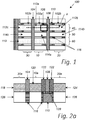
- Figure 1 is a plan (top-down) view of a semiconductor structure 100 comprising three FET device regions 10, 20, 30, during formation of the FET 30 devices. Specifically, Figure 1 shows the semiconductor structure 100 at a stage of formation of the FET devices after etch-back of the contact material layer leading to formation of individual contacts 112a-c, 113.
- the semiconductor structure 100 comprises a first FET device region 10 in which a first transistor structure is formed, a second FET device region 20 in which a second transistor structure is formed and a third FET device region 30 in which a third transistor structure is formed.
- Each of the FET device regions 10, 20, 30 comprises a first source/drain region 40, a channel region 50 and a second source/drain region 60.
- Each of the transistor structures comprise a plurality of stacked nanosheets 102a-c of which only the topmost nanosheet is visible in the illustration.
- the plurality of nanosheets 102a-c form a channel structure separating the first source/drain portion (formed in the first source/drain region 40) of the transistor structure from a second source/drain portion (formed in the second source/drain region 60) of the transistor structure.
- the second transistor structure is separated from the first transistor structure by a first trench.
- a first dielectric wall 108 is formed in the trench at a distance from a sidewall of the first transistor structure, and at a distance from a sidewall of the second transistor structure.
- a buried power rail 110 is formed in the substrate.
- An isolating material 116 is formed at sidewalls of the BPR 110, within the substrate.
- the third transistor structure is separated from the first transistor structure by a second trench, which has a smaller width than the first trench.
- a second dielectric wall 104 is formed in the second trench. Specifically, the second dielectric wall 104 is formed filling the second trench.
- the first FET device region 10 and the third FET device region 30 may together form a pair or a cell.
- the second FET device region 20 may form a pair or a cell with a further FET device region (not depicted) on the opposite side of the second FET device region 20.
- a BPR 110 may be formed in the substrate. A BPR is often not formed within a pair/cell.
- a first gate structure 114a extends in the channel region 50, across the channel structure formed by the stack of nanosheets 102a of the first transistor structure.
- a second gate structure 114b extends in the channel region 50 across the channel structure formed by the stack of nanosheets 102b of the second transistor structure.
- a third gate structure 114c extends in the channel region 50, across the channel structure formed by the stack of nanosheets 102c of the first transistor structure.
- a first set of contacts 112a-c have been formed in the first source/drain region 40. The first contact 112a extends between the second dielectric wall 104 and the first dielectric wall 108, across the source/drain portion of the first transistor structure, and into the trench.
- the second contact 112b extends from the first dielectric wall 108, across the trench and the first source/drain portion of the second transistor structure.
- the third contact 112c extends from the second dielectric wall 104, across the source/drain portion of the third transistor structure.
- a second set of contacts 113 extend in a similar manner in the second source/drain region 60, across the second source/drain portions of the transistor structures.
- a black rectangle indicates a via 106 to the BPR 110. This represents where a via 106 is formed connecting the contact material 112a to the BPR 110.
- Figures 2a-7b show in perspective a section of the substrate 126 through a first source/drain portion of the FET device regions, along the dashed line A of Figure 1 .
- the illustrated planes of section extending through the structure 100 are common to all the figures, unless indicated otherwise.
- Figure 2a shows a substrate 126, on which a first transistor structure, a second transistor structure and a third transistor structure is formed.
- the substrate 126 is a semiconductor substrate, i.e. a substrate comprising at least one semiconductor layer.
- the substrate 126 may be a single-layered semiconductor substrate, for instance formed by a bulk substrate.
- the substrate 126 may however also be a multi-layered substrate, for instance formed by an epitaxially grown semiconductor layer on a bulk substrate, or a semiconductor-on-insulator (SOI) substrate.
- SOI semiconductor-on-insulator
- a first transistor structure has been formed in a first FET device region 10a.
- a first source/drain portion 120 of the first transistor structure is visible in the figures.
- a second transistor structure has been formed in a second FET device region 20a.
- a first source/drain portion 124 of the second transistor structure is visible in Figure 2a .
- the first and second transistor structures are separated by a trench.
- spacers 122 have been formed at a sidewall of the first source/drain portion 120 of the first transistor structure and at a sidewall of the first source/drain portion 124 of the second transistor structure. It will be appreciated that the spacers 122 may extend in a direction along the trench and the first and second transistor structures.
- the material of the spacers 122 may be conformally deposited over the first transistor structure and the second transistor structure, before being anisotropically (top-down) etched to form the spacers 122.
- the spacer material may for example be SiN, SiCO, or SiCN.
- the spacer material is conformally deposited by means of for example ALD and CVD.
- a third transistor structure has been formed in a third FET device region 30a.
- a first source/drain portion 118 of the second transistor structure is visible in Figure 2a .
- the third transistor structure is separated from the first transistor structure by a second trench which has a smaller width than the first trench which separates the first transistor structure and the second transistor structure.
- a dielectric wall 104 has been formed protruding above a top surface of the transistor structures.
- the dielectric wall 104 may for example be formed from SiN, SiCO, or SiCN.
- the source/drain portions 118, 120, 124 may form source/drain terminals of the final FET devices.
- the first source/drain region 118 of the third transistor structure is formed by an n-doped selective epitaxial silicon or silicon carbon process, using for instance P, As or Sb as dopants, whereas the first source/drain regions 120, 124 of the first and the second transistor structures are formed by a p-doped selective epitaxial silicon or silicon germanium process. In the latter example, B or Ga may be used as dopants.
- the dielectric wall 104 may facilitate separation between the NMOS and the PMOS devices formed in this process.
- the substrate 126 may be etched through the trenches separating the respective transistor structures. Substrate trenches may thus be formed in the substrate 126. As is shown in Figure 2a , a buried power rail (BPR) 110 may be formed in the substrate trench between the first transistor structure and the second transistor structure. As further shown in Figure 2a , the trenches formed in the underlying thickness portion of the substrate 126 (the substrate trenches) may be filled with an isolating material 116, thereby separating the FET device regions 10a, 20a, 30a of the substrate 100, on which the FET devices are formed, using shallow trench isolation (STI).
- STI shallow trench isolation
- a dielectric/isolating cap 128 may be formed over the BPR 110.
- the dielectric cap may be formed from a different dielectric/isolating material than the isolating material 116.
- the dielectric/isolating cap may be formed of a material which may be selectively etched relative to the isolating (STI) material 116.
- the semiconductor structure shown in Figure 2a may be a starting position for forming a forksheet FET device, in accordance with some embodiments.
- Figure 2b shows a starting position for forming a nanosheet FET device, in accordance with other embodiments.
- Figure 2b also shows a substrate 126, on which a first transistor structure, a second transistor structure and a third transistor structure is formed.
- the first transistor structure formed in the first FET device region 10b, the second transistor structure formed in the second FET device region 20b, and the trench and structures between them may be equivalent to the corresponding features in Figure 2a .
- the third transistor structure formed in the third FET device region 30b is separated from the first transistor structure by a third trench.
- second spacers 122a have been formed at a sidewall of the first source/drain portion 118 of the third transistor structure and at a sidewall of the first source/drain portion 120 of the first transistor structure. It will be appreciated that the second spacers 122a may also extend in a direction along the trench and the first and third transistor structures.
- a third dielectric wall 109 has been formed in the third trench, between the second spacers.
- the second spacers 122a and the third dielectric wall 109 may be equivalent to, and be formed in a similar manner as, the spacers 122 and the first dielectric wall 108 described with reference to Figure 2b .
- the second substrate trench has been filled with an isolating material 116.
- an interlayer dielectric 130 has been formed over the semiconductor structure and filling the trench.
- the interlayer dielectric 130 may be formed by the same material as the isolating material 116 forming the STI. It will be appreciated that the application of the interlayer dielectric 130 may be optional.
- sacrificial gate structures which may have been formed in the channel regions 50 of the different transistor structures may be replaced with final gate structures 114a-c. It will however be appreciated that a replacement gate procedure may take place during other steps of the formation of the semiconductor structure.
- the interlayer dielectric has been removed from a region of the semiconductor structure which includes the present cross-section.
- the first source/drain portion 118, 120, 124, the dielectric walls 104, 108 and portions of the dielectric cap 128 and the isolating material in the trench are exposed.
- a mask layer 132 has been applied to (formed over) the semiconductor structure.
- the mask layer 132 comprises an opening 134 which exposes (at least) a portion of the first source/drain portion 120 of the first transistor structure.
- the opening 134 further exposes a portion of the first dielectric wall 108, and a portion of the trench between the first source/drain portion 120 of the first transistor structure and the first dielectric wall 108.
- the mask layer 132 covers another portion of the first dielectric wall 108.
- the dielectric cap 128 has been selectively etched using the exposed portion of the trench as an etch mask. A portion of the BPR 110 is thus exposed in the bottom of the trench. The etch has also removed a small portion of the BPR 110, which is optional. The isolating material 116 has not been etched and may reduce the risk of a short connection between the BPR 110 and the subfin/substrate of the first transistor structure.
- a contact material layer 136 has been deposited across the first source/drain region 40 of the transistor structures.
- the contact material layer 136 may be deposited using for example atomic layer deposition (ALD), chemical vapor deposition (CVD), physical vapor deposition (PVD) or plating.
- ALD atomic layer deposition
- CVD chemical vapor deposition
- PVD physical vapor deposition
- Possible metals in contact metallization include for example titanium (Ti), nickel (Ni), nickel-platinum (NiPt), tungsten (W), cobalt (Co), ruthenium (Ru), molybdenum (Mo), titanium nitride (TiN), and tungsten nitride (WN).
- the contact material layer 136 may have been deposited in a continuous line in the first source/drain region 40 of the transistor structures.
- the contact material layer 112 is in contact with the BPR 110 and the first source/drain portion 120 of the first transistor structure.
- the contact material layer 136 has been etched back below a top surface of the first dielectric wall 108 and below a top surface of the second dielectric wall 104.
- the contact material layer has been divided into three contacts 112a-c.
- the first contact 112a is contacting the BPR 110 and wraps around the top and a sidewall of the first source/drain portion 120 of the first transistor structure.
- the second contact 112b is separated from the first contact 112a by the first dielectric wall 108.
- the second contact 112b wraps around the top and a sidewall of the first source/drain portion 124 of the second transistor structure.
- the isolating material 116 and the dielectric/isolating cap 128 isolate the second contact 112b from the BPR 110.
- the third contact 112c is separated from the first contact 112a by the second dielectric wall 104.
- the third contact is in connection with the first source/drain portion 118 of the third transistor structure.
- Figure 7b shows a semiconductor structure allowing for formation of nanosheet FET devices similar to that of Figure 2b .
- Figure 7b shows the semiconductor structure after etch-back of the contact material layer.
- Figure 7b shows a situation equivalent to that of Figure 7a , except that the third transistor structure is separated from the first transistor structure by a third trench having a third dielectric wall 109, like in Figure 2b .
- the first contact 112d wraps around a sidewall of the first source/drain portion 120 of the first transistor structure.
- the contact 112d wraps around at least the top and two sidewalls of the first source/drain portion 120 of the first transistor structure.
- the third contact 112e at least wraps around the top and a portion of the sidewall which faces the third trench of the first source/drain portion 118 of the third transistor structure.
- the third contact 112e is separated from the first contact 112d by the third dielectric wall 109.
- Figure 8a shows a cross-section through a channel region of a walled forksheet transistor structure.
- the illustration in Figure 8a may correspond to a cross-section taken through the channel region 50 of Figure 1 .
- the three pluralities of stacked nanosheets 102a-c, the dielectric walls 104, 108 and the substrate 126 are shown.
- Figure8 shows a cross-section through a channel region of a nanosheet transistor structure, such as the nanosheet transistor structures illustrated in Figures 2b and 7b .
- a nanosheet transistor structure such as the nanosheet transistor structures illustrated in Figures 2b and 7b .
- Figure8 shows a cross-section through a channel region of a nanosheet transistor structure, such as the nanosheet transistor structures illustrated in Figures 2b and 7b .
- the nanosheet transistor structures illustrated in Figures 2b and 7b For illustrative purposes, only the three pluralities of stacked nanosheets 102d, 102b, 102e, the dielectric walls 108, 109 and the substrate 126 are shown.
- the plurality of horizontally stacked nanosheets 102a, 102d in the first FET device region 10a-b is separated from the plurality of horizontally stacked nanosheets 102b in the second FET device region 20a-b by a trench comprising a first dielectric wall 108.
- the first dielectric wall 108 may improve the electrical isolation between the FET devices formed in the first FET device region 10a and the second FET device region 20a.
- the second dielectric wall 104 is formed between the plurality of horizontally stacked nanosheets 102a in the first FET device region 10a and the plurality of horizontally stacked nanosheets 102c in the third FET device region 30a.
- the two stacks of nanosheets 102a, 102c and the second dielectric wall 104 thus form a forklike structure.
- the second dielectric wall 104 may provide increased electrical isolation between the nanosheets 102a of the first transistor structure and the nanosheets 120c of the third transistor structure.
- the first FET device formed in the first FET device region 10a and the third FET device formed in the third FET device region 30c may be formed more closely together (i.e. with a shorter distance/pitch between them) on the substrate 126.
- Gate structures may be formed partially wrapping around the nanosheets 102a, 102c of the first and third transistor structures since nanosheets 102a, 102c are only attached to a wall on one side.
- the stack of nanosheets 102d in the first FET device region 10b is separated from the stack of nanosheets 102b formed in the second FET device region 20b by a first trench comprising a first dielectric wall 108.
- the stack of nanosheets 102e in the third FET device region 30b is separated from the stack of nanosheets 102d in the first FET device region 10b by a second trench comprising a third dielectric wall 109.
- both sides of the stacks of nanosheets 102b, 102d, 102e are free (i.e.
- a gate may be formed wrapping fully around the nanosheets 102b, 102d, 102e.
- a gate wrapping fully around channel structure i.e. being formed around and between the nanosheets) may improve control of the horizontally oriented flow of charge carriers between the source and drain portions within the final FET device.
Landscapes
- Element Separation (AREA)
- Chemical & Material Sciences (AREA)
- Engineering & Computer Science (AREA)
- Nanotechnology (AREA)
- Insulated Gate Type Field-Effect Transistor (AREA)
- Metal-Oxide And Bipolar Metal-Oxide Semiconductor Integrated Circuits (AREA)
Abstract
Description
- The present inventive concept relates to the field of forming semiconductor devices.
- In the strive to provide even more power- and area-efficient circuit designs, new transistor devices are being developed.
- Horizontal channel field effect transistor (FET) devices include the finFET, which has a gate straddling a channel portion of a fin-shaped semiconductor structure, and the horizontal nanowire- or nanosheet-FET (horizontal NWFET or NSFET), which has a gate at least partly enclosing a channel portion of a horizontally oriented nanowire- or nanosheet-shaped semiconductor structure.
- Efficient process flows dedicated to fabrication of horizontal channel FET devices have been developed. However, the objective of developing more area efficient FET devices using more convenient fabrication methods still remains.
- An objective of the present disclosure is therefore to provide an improved method for forming a semiconductor structure including FET devices.
- According to an aspect of the present disclosure, there is provided a method for forming a semiconductor device comprising a first field-effect transistor, FET, device and a second FET device, the method comprising:
- forming, on a semiconductor substrate, a first transistor structure and a second transistor structure separated by a first trench, the first trench comprising a first dielectric wall protruding above a top surface of the transistor structures,
wherein each of the first and the second transistor structures comprises a plurality of stacked nanosheets forming a channel structure, and a source portion and a drain portion horizontally separated by said channel structure; - depositing a contact material over the transistor structures and the first dielectric wall, thereby filling the first trench and contacting a first source/drain portion of the first transistor structure and a first source/drain portion of the second transistor structure; and
- etching back the contact material layer below a top surface of the first dielectric wall, thereby forming a first contact contacting the first source/drain portion of the first transistor structure, and a second contact contacting the first source/drain portion of the second transistor structure.
- Throughout this disclosure, the term transistor structure will refer to a semiconductor structure from which a transistor (or FET device) may be formed. Each of the transistor structures and thus, in the end, the final FET devices comprise a plurality of horizontally stacked nanosheets.
- Each of the transistor structures may form, or be arranged to subsequently form, a FET device. By a channel FET device is hereby meant a device comprising a semiconductor structure comprising a first and a second source/drain portion and a channel portion located intermediate and extending between the first and second source/drain portions, and further comprising a gate structure extending along the channel portion. In a horizontal channel FET device, the first and second source/drain portions and the channel portion may intersect a common horizontal plane. The channel portion is adapted to (in use of the device) conduct a flow of charge carriers between the source/drain.
- As used herein, the term "vertical" denotes a direction or orientation (e.g. of a surface, a dimension or other feature) parallel to a normal to the substrate (i.e. a main plane of extension or main/upper surface thereof). The term "horizontal" meanwhile denotes a direction or orientation parallel to the substrate (i.e. a main plane of extension or main surface thereof), or equivalently transverse to the vertical direction. Meanwhile, terms such as "above", "upper", "top" and "below", "lower", "bottom" refer to relative positions as viewed along the vertical direction and does hence not imply an absolute orientation of the substrate or device.
- Through the etch-back of the contact material layer below the top surface of the first dielectric wall, the contact material layer is divided into a first contact and a second contact separated by the first dielectric wall. The first contact is contacting the first source/drain region of the first transistor structure. The second contact is contacting the first source/drain portion of the second transistor structure. Specifically, as the contact material is formed across the source/drain portions of the first transistor structure and the second transistor structure and in the first trench, the first contact may wrap around at least two surfaces of the first source/drain portion of the first transistor structure, and the first contact may wrap around at least two surfaces of the first source/drain portion of the second transistor structure. Thus, the method may comprise depositing the contact material to form wrap-around contacts. A wrap-around contact may improve the control of the contact on the source/drain portion.
- As the contact material is etched back below the top surface of the first dielectric wall, the size and position of the contacts may be defined by the first dielectric wall. The contacts may thus be formed self-aligned with the first trench and the first source/drain portions.
- Moreover, the distance between adjacent contacts is limited by the width of the first dielectric wall. Thus, the separation of the contacts may be controlled by the width of the first dielectric wall.
- Using the above-defined method, the contacts may be formed with higher accuracy. The contacts may also be formed with a smaller pitch (distance) between them. The above-defined method may thus reduce the size of the resulting FET devices.
- According to an embodiment, the first FET device and the second FET device may be of the same dopant type.
- For example, both the first FET device and the second FET device may be p-type FET devices. Alternatively, both the first FET device and the second FET device may be n-type FET devices.
- It will be appreciated that the first FET device and the second FET device may also be of the opposite dopant type.
- According to an embodiment, depositing a contact material may comprise depositing said contact material in a continuous line extending in a direction from the first source direction from the first source/drain portion of the first transistor structure towards the first source/drain portion of the second transistor structure, across the transistor structures, the first trench and the first dielectric wall.
- The contact material may thus be deposited such that a continuous line is formed in the horizontal plane across from the first source/drain portion of the first transistor structure towards a first source/drain portion of the second transistor structure.
- Applying the contact material in a continuous line across (a source/drain region of) both transistor structures and then etching back the contact material below a top surface of the first dielectric wall to divide the contact material line into individual contacts may facilitate the formation of the contacts. Forming a continuous line of contact material and dividing it into individual contacts may for example be more convenient than applying the material as discrete contacts. Specifically, such a method may provide that smaller contacts may be formed with a higher accuracy.
- According to an embodiment, forming the dielectric wall may comprise forming spacers in the first trench at sidewalls of the first transistor structure and the second transistor structure. The spacers may protrude above a top surface of the transistor structures. Forming the first dielectric wall may further comprise forming the first dielectric wall in the first trench between the spacers and removing the spacers.
- For example, the spacer material may be formed conformally in the trench, and then anisotropically (top-down) etched to form the spacers. The dielectric wall may be formed by filling a gap between the spacers with a dielectric material. The spacers may for example be removed using a selective etch.
- Forming spacers on the sidewalls of the first and second transistor structure and then forming the first dielectric wall between the spacers may provide that the dielectric wall is formed self-aligned between the transistor structures.
- According to an embodiment, forming the first transistor structure and the second transistor structure may comprise, prior to the formation of the first dielectric wall, etching the substrate through the trench, thereby forming a substrate trench, and forming a buried power rail (BPR) in the substrate trench.
- The method may further comprise, prior to depositing the contact material layer, applying a mask layer including an opening which exposes at least a portion of the first source/drain portion of the first transistor structure. The mask layer may further expose a portion of the trench between the first transistor structure and the first dielectric wall, and a portion of the first dielectric wall. The mask layer may cover at least another portion of the first dielectric wall. The method may further comprise exposing the BPR in the bottom of the trench by etching through the exposed portion of the first trench and removing the mask layer.
- The BPR may be embedded in, or covered with, a dielectric or isolating material. For example, in the substrate trench, the BPR may be covered, at least on a sidewall facing the first transistor structure, by a first dielectric material. On a top surface of the BPR, a dielectric cap may be formed of a second dielectric material. The BPR may be exposed in the bottom of the trench by selectively etching the second dielectric material of the dielectric cap, while not etching the first dielectric material. The first dielectric material may thus decrease the risk of a short connection between the BPR and the portion of the substrate (or subfin) on which the first transistor structure is formed.
- In embodiments in which a BPR is formed in the substrate and exposed prior to the deposition of the contact material, the contact may be a contact between the BPR and the first source/drain portion of the first transistor structure.
- According to an embodiment, the method may further comprise forming a third transistor structure on the semiconductor substrate. The third transistor structure may be separated from the first transistor structure by a second trench. The second trench may have a width smaller than the width of the first trench.
- The third transistor structure may comprise a plurality of stacked nanosheets forming a channel structure. The third transistor structure may further comprise a source portion and a drain portion. The source portion and the drain portion may be horizontally separated by the channel structure.
- The method may further comprise forming a second dielectric wall filling the second trench. The second dielectric wall may protrude above a top surface of the transistor structures. The method may further comprise etching back the contact material layer below a top surface of the second dielectric wall.
- The first and the third transistor structure may together form a forksheet transistor structure. In such structures, two neighboring FET devices are separated by a dielectric wall. A dielectric wall between two FET devices may allow for electrical separation/isolation between the FET devices with a shorter distance/pitch between the FET devices. Thus, the resulting FET devices may be more closely arranged on the substrate.
- According to an embodiment, the method may further comprise forming a third transistor structure on the semiconductor substrate. The third transistor structure may be separated from the first transistor structure by a third trench. The third trench may comprise a third dielectric wall which may protrude above a top surface of the transistor structures.
- The third transistor structure may comprise a plurality of stacked nanosheets which may form a channel structure. The third transistor structure may further comprise a source portion and a drain portion. The source portion and the drain portion may be horizontally separated by the channel structure.
- The method may further comprise etching back the contact material layer below a top surface of the second dielectric wall.
- The third transistor structure may form a third FET device. Methods in accordance with this embodiment may provide that the resulting FET devices are nanosheet FET devices. Such FET devices may comprise a wrap-around gate, which wraps around the channel structure of the FET device. A wrap-around gate may provide improved control of the horizontally oriented flow of charge carriers through the channel structure between the source and drain portions of the FET device.
- According to an embodiment, a third FET device, which may be formed from the third transistor structure, may be a FET device of a different dopant type than the first FET device.
- According to an embodiment, forming the first semiconductor structure and the second semiconductors structure on the substrate may comprise, prior to forming the first dielectric wall, forming a substrate trench by etching the substrate through the first trench. The method may further comprise filling the substrate trench with an isolating material.
- Forming a trench in the substrate between neighboring transistor structures, and filling the trench with an isolating material, may improve electrical separation/isolation of the transistor structures (and final transistor devices) through the substrate.
- It will be appreciated that, according to some embodiments, the method may comprise forming a BPR in the substrate trench prior to filling the substrate trench with an isolating material. Alternatively, the method may comprise forming a BPR in the substrate trench after filling the substrate trench with an isolating material.
- According to an embodiment, the method may further comprise, prior to forming the contact material layer, forming an interlayer dielectric over the transistor structures and the first dielectric wall, and filling the first trench. The method may further comprise removing the interlayer dielectric in a region extending between the first source/drain portion of the first transistor structure and the first source/drain portion of the second transistor structure across the first dielectric wall and the first trench.
- It will be appreciated that the interlayer dielectric may be kept at other regions of the transistor structures and the first trench. Providing an interlayer dielectric across the transistor structures and the (first) trench, and then removing portions of the interlayer dielectric in a specific region may provide an opening in the interlayer dielectric layer. The opening may be formed to expose portions of the transistor structures, substrate and/or BPR etc. which the contact material layer is intended to be in contact with. Thus, the interlayer dielectric may provide increased precision in the application of the contact material.
- According to an embodiment, each of the transistor structure may comprise a sacrificial gate structure extending across the channel structures. The method may further comprise, prior to removing the interlayer dielectric in the abovementioned region, replacing the sacrificial gate structure with a final gate structure.
- It is noted that other embodiments using all possible combinations of features recited in the above described embodiments may be envisaged. Thus, the present disclosure also relates to all possible combinations of features mentioned herein. Any embodiment described herein may be combinable with other embodiments also described herein, and the present disclosure relates to all combinations of features.
- The above, as well as additional objects, features and advantages of the present inventive concept, will be better understood through the following illustrative and non-limiting detailed description, with reference to the appended drawings. In the drawings like reference numerals will be used for like elements unless stated otherwise.
-
Figure 1 is a plan view of a semiconductor structure, in accordance with some embodiments. -
Figures 2a-7b illustrate a method of forming a semiconductor device, in accordance with some embodiments. -
Figures 8a and 8b illustrate cross-sections of the channel structures of different transistor structures, in accordance with some embodiments. - A method for forming a semiconductor device will now be described with reference to the figures. Reference will throughout be made to a first field-effect transistor, FET,
device region 10, a secondFET device region 20 and a thirdFET device region 30, of asemiconductor substrate 126. Each of theFET device regions FET device region - As may be appreciated, the
substrate 126 and thetransistor structure regions -
Figure 1 is a plan (top-down) view of asemiconductor structure 100 comprising threeFET device regions FET 30 devices. Specifically,Figure 1 shows thesemiconductor structure 100 at a stage of formation of the FET devices after etch-back of the contact material layer leading to formation ofindividual contacts 112a-c, 113. - The
semiconductor structure 100 comprises a firstFET device region 10 in which a first transistor structure is formed, a secondFET device region 20 in which a second transistor structure is formed and a thirdFET device region 30 in which a third transistor structure is formed. Each of theFET device regions drain region 40, achannel region 50 and a second source/drain region 60. - Each of the transistor structures comprise a plurality of stacked nanosheets 102a-c of which only the topmost nanosheet is visible in the illustration. In each transistor structure, the plurality of nanosheets 102a-c form a channel structure separating the first source/drain portion (formed in the first source/drain region 40) of the transistor structure from a second source/drain portion (formed in the second source/drain region 60) of the transistor structure.
- The second transistor structure is separated from the first transistor structure by a first trench. A first
dielectric wall 108 is formed in the trench at a distance from a sidewall of the first transistor structure, and at a distance from a sidewall of the second transistor structure. In the bottom of the first trench, a buriedpower rail 110 is formed in the substrate. An isolatingmaterial 116 is formed at sidewalls of theBPR 110, within the substrate. - The third transistor structure is separated from the first transistor structure by a second trench, which has a smaller width than the first trench. In the second trench, a second
dielectric wall 104 is formed. Specifically, the seconddielectric wall 104 is formed filling the second trench. - The first
FET device region 10 and the thirdFET device region 30 may together form a pair or a cell. The secondFET device region 20 may form a pair or a cell with a further FET device region (not depicted) on the opposite side of the secondFET device region 20. Between each pair/cell, aBPR 110 may be formed in the substrate. A BPR is often not formed within a pair/cell. - A
first gate structure 114a extends in thechannel region 50, across the channel structure formed by the stack of nanosheets 102a of the first transistor structure. Asecond gate structure 114b extends in thechannel region 50 across the channel structure formed by the stack ofnanosheets 102b of the second transistor structure. And athird gate structure 114c extends in thechannel region 50, across the channel structure formed by the stack ofnanosheets 102c of the first transistor structure. A first set ofcontacts 112a-c have been formed in the first source/drain region 40. Thefirst contact 112a extends between the seconddielectric wall 104 and the firstdielectric wall 108, across the source/drain portion of the first transistor structure, and into the trench. Thesecond contact 112b extends from the firstdielectric wall 108, across the trench and the first source/drain portion of the second transistor structure. Thethird contact 112c extends from the seconddielectric wall 104, across the source/drain portion of the third transistor structure. - A second set of
contacts 113 extend in a similar manner in the second source/drain region 60, across the second source/drain portions of the transistor structures. - A black rectangle indicates a via 106 to the
BPR 110. This represents where a via 106 is formed connecting thecontact material 112a to theBPR 110. -
Figures 2a-7b show in perspective a section of thesubstrate 126 through a first source/drain portion of the FET device regions, along the dashed line A ofFigure 1 . The illustrated planes of section extending through thestructure 100 are common to all the figures, unless indicated otherwise. -
Figure 2a shows asubstrate 126, on which a first transistor structure, a second transistor structure and a third transistor structure is formed. Thesubstrate 126 is a semiconductor substrate, i.e. a substrate comprising at least one semiconductor layer. Thesubstrate 126 may be a single-layered semiconductor substrate, for instance formed by a bulk substrate. Thesubstrate 126 may however also be a multi-layered substrate, for instance formed by an epitaxially grown semiconductor layer on a bulk substrate, or a semiconductor-on-insulator (SOI) substrate. - As is further shown in
Figure 2a , a first transistor structure has been formed in a firstFET device region 10a. A first source/drain portion 120 of the first transistor structure is visible in the figures. - A second transistor structure has been formed in a second
FET device region 20a. A first source/drain portion 124 of the second transistor structure is visible inFigure 2a . - The first and second transistor structures (represented by their respective first source/
drain portions 120, 124) are separated by a trench. In thetrench 122,spacers 122 have been formed at a sidewall of the first source/drain portion 120 of the first transistor structure and at a sidewall of the first source/drain portion 124 of the second transistor structure. It will be appreciated that thespacers 122 may extend in a direction along the trench and the first and second transistor structures. - For example, the material of the
spacers 122 may be conformally deposited over the first transistor structure and the second transistor structure, before being anisotropically (top-down) etched to form thespacers 122. The spacer material may for example be SiN, SiCO, or SiCN. Preferably, the spacer material is conformally deposited by means of for example ALD and CVD. - A third transistor structure has been formed in a third
FET device region 30a. A first source/drain portion 118 of the second transistor structure is visible inFigure 2a . The third transistor structure is separated from the first transistor structure by a second trench which has a smaller width than the first trench which separates the first transistor structure and the second transistor structure. In the third trench between the first and third transistor structures, adielectric wall 104 has been formed protruding above a top surface of the transistor structures. Thedielectric wall 104 may for example be formed from SiN, SiCO, or SiCN. - The source/
drain portions drain region 118 of the third transistor structure is formed by an n-doped selective epitaxial silicon or silicon carbon process, using for instance P, As or Sb as dopants, whereas the first source/drain regions dielectric wall 104 may facilitate separation between the NMOS and the PMOS devices formed in this process. - Prior to the formation of the
spacers 122 and thedielectric walls substrate 126 may be etched through the trenches separating the respective transistor structures. Substrate trenches may thus be formed in thesubstrate 126. As is shown inFigure 2a , a buried power rail (BPR) 110 may be formed in the substrate trench between the first transistor structure and the second transistor structure. As further shown inFigure 2a , the trenches formed in the underlying thickness portion of the substrate 126 (the substrate trenches) may be filled with an isolatingmaterial 116, thereby separating theFET device regions substrate 100, on which the FET devices are formed, using shallow trench isolation (STI). - A dielectric/isolating
cap 128 may be formed over theBPR 110. The dielectric cap may be formed from a different dielectric/isolating material than the isolatingmaterial 116. Specifically, the dielectric/isolating cap may be formed of a material which may be selectively etched relative to the isolating (STI)material 116. - The semiconductor structure shown in
Figure 2a may be a starting position for forming a forksheet FET device, in accordance with some embodiments.Figure 2b , on the other hand, shows a starting position for forming a nanosheet FET device, in accordance with other embodiments. -
Figure 2b also shows asubstrate 126, on which a first transistor structure, a second transistor structure and a third transistor structure is formed. As is shown inFigure 2b , the first transistor structure formed in the firstFET device region 10b, the second transistor structure formed in the secondFET device region 20b, and the trench and structures between them may be equivalent to the corresponding features inFigure 2a . - In
Figure 2b , the third transistor structure formed in the thirdFET device region 30b, is separated from the first transistor structure by a third trench. In the third trench,second spacers 122a have been formed at a sidewall of the first source/drain portion 118 of the third transistor structure and at a sidewall of the first source/drain portion 120 of the first transistor structure. It will be appreciated that thesecond spacers 122a may also extend in a direction along the trench and the first and third transistor structures. A thirddielectric wall 109 has been formed in the third trench, between the second spacers. Thesecond spacers 122a and the thirddielectric wall 109 may be equivalent to, and be formed in a similar manner as, thespacers 122 and the firstdielectric wall 108 described with reference toFigure 2b . - Further, prior to the formation of the
second spacers 122 and the thirddielectric wall 109, a second substrate trench has been formed in the substrate between the first and the third transistor structures, the second substrate trench has been filled with an isolatingmaterial 116. - In the following, the method will be described with reference to figures showing the structure of
Figure 2a . However, the same method may be applied to structures like the one described with reference toFigure 2b . - In
Figure 3 , aninterlayer dielectric 130 has been formed over the semiconductor structure and filling the trench. Theinterlayer dielectric 130 may be formed by the same material as the isolatingmaterial 116 forming the STI. It will be appreciated that the application of theinterlayer dielectric 130 may be optional. - At this point during the formation of the semiconductor structure, sacrificial gate structures which may have been formed in the
channel regions 50 of the different transistor structures may be replaced withfinal gate structures 114a-c. It will however be appreciated that a replacement gate procedure may take place during other steps of the formation of the semiconductor structure. - In
Figure 4 , the interlayer dielectric has been removed from a region of the semiconductor structure which includes the present cross-section. Thus, at least portions of the first source/drain portion dielectric walls dielectric cap 128 and the isolating material in the trench are exposed. - In
Figure 5 , amask layer 132 has been applied to (formed over) the semiconductor structure. Themask layer 132 comprises anopening 134 which exposes (at least) a portion of the first source/drain portion 120 of the first transistor structure. Theopening 134 further exposes a portion of the firstdielectric wall 108, and a portion of the trench between the first source/drain portion 120 of the first transistor structure and the firstdielectric wall 108. Themask layer 132 covers another portion of the firstdielectric wall 108. - As is further shown in
Figure 5 , in the bottom of the trench, thedielectric cap 128 has been selectively etched using the exposed portion of the trench as an etch mask. A portion of theBPR 110 is thus exposed in the bottom of the trench. The etch has also removed a small portion of theBPR 110, which is optional. The isolatingmaterial 116 has not been etched and may reduce the risk of a short connection between theBPR 110 and the subfin/substrate of the first transistor structure. - In
Figure 6 , acontact material layer 136 has been deposited across the first source/drain region 40 of the transistor structures. Thecontact material layer 136 may be deposited using for example atomic layer deposition (ALD), chemical vapor deposition (CVD), physical vapor deposition (PVD) or plating. Possible metals in contact metallization include for example titanium (Ti), nickel (Ni), nickel-platinum (NiPt), tungsten (W), cobalt (Co), ruthenium (Ru), molybdenum (Mo), titanium nitride (TiN), and tungsten nitride (WN). - The
contact material layer 136 may have been deposited in a continuous line in the first source/drain region 40 of the transistor structures. - Specifically, the contact material layer 112 is in contact with the
BPR 110 and the first source/drain portion 120 of the first transistor structure. - In
Figure 7a , thecontact material layer 136 has been etched back below a top surface of the firstdielectric wall 108 and below a top surface of the seconddielectric wall 104. Thus, the contact material layer has been divided into threecontacts 112a-c. Thefirst contact 112a is contacting theBPR 110 and wraps around the top and a sidewall of the first source/drain portion 120 of the first transistor structure. - The
second contact 112b is separated from thefirst contact 112a by the firstdielectric wall 108. Thesecond contact 112b wraps around the top and a sidewall of the first source/drain portion 124 of the second transistor structure. The isolatingmaterial 116 and the dielectric/isolatingcap 128 isolate thesecond contact 112b from theBPR 110. - The
third contact 112c is separated from thefirst contact 112a by the seconddielectric wall 104. The third contact is in connection with the first source/drain portion 118 of the third transistor structure. -
Figure 7b shows a semiconductor structure allowing for formation of nanosheet FET devices similar to that ofFigure 2b .Figure 7b shows the semiconductor structure after etch-back of the contact material layer. Thus,Figure 7b shows a situation equivalent to that ofFigure 7a , except that the third transistor structure is separated from the first transistor structure by a third trench having a thirddielectric wall 109, like inFigure 2b . In the third trench, as is shown inFigure 7b , thefirst contact 112d, wraps around a sidewall of the first source/drain portion 120 of the first transistor structure. Thus, thecontact 112d wraps around at least the top and two sidewalls of the first source/drain portion 120 of the first transistor structure. - The
third contact 112e at least wraps around the top and a portion of the sidewall which faces the third trench of the first source/drain portion 118 of the third transistor structure. Thethird contact 112e is separated from thefirst contact 112d by the thirddielectric wall 109. - With reference to
Figures 8a and 8b , differences between a walled forksheet transistor structure and a walled nanosheet transistor structure will be described. -
Figure 8a shows a cross-section through a channel region of a walled forksheet transistor structure. For example, the illustration inFigure 8a may correspond to a cross-section taken through thechannel region 50 ofFigure 1 . For illustrative purposes, only the three pluralities of stacked nanosheets 102a-c, thedielectric walls substrate 126 are shown. -
Figure8 shows a cross-section through a channel region of a nanosheet transistor structure, such as the nanosheet transistor structures illustrated inFigures 2b and7b . For illustrative purposes, only the three pluralities of stackednanosheets dielectric walls substrate 126 are shown. - In both
Figures 8a and 8b , the plurality of horizontally stacked nanosheets 102a, 102d in the firstFET device region 10a-b is separated from the plurality of horizontally stackednanosheets 102b in the secondFET device region 20a-b by a trench comprising a firstdielectric wall 108. The firstdielectric wall 108 may improve the electrical isolation between the FET devices formed in the firstFET device region 10a and the secondFET device region 20a. - In Figure 9a, the second
dielectric wall 104 is formed between the plurality of horizontally stackednanosheets 102a in the firstFET device region 10a and the plurality of horizontally stackednanosheets 102c in the thirdFET device region 30a. The two stacks of nanosheets 102a, 102c and the seconddielectric wall 104 thus form a forklike structure. - The second
dielectric wall 104 may provide increased electrical isolation between the nanosheets 102a of the first transistor structure and the nanosheets 120c of the third transistor structure. Thus, the first FET device formed in the firstFET device region 10a and the third FET device formed in the third FET device region 30c may be formed more closely together (i.e. with a shorter distance/pitch between them) on thesubstrate 126. - Gate structures may be formed partially wrapping around the nanosheets 102a, 102c of the first and third transistor structures since nanosheets 102a, 102c are only attached to a wall on one side.
- As in
Figure 8a , inFigure 8b , the stack ofnanosheets 102d in the firstFET device region 10b is separated from the stack ofnanosheets 102b formed in the secondFET device region 20b by a first trench comprising a firstdielectric wall 108. Further, the stack of nanosheets 102e in the thirdFET device region 30b is separated from the stack ofnanosheets 102d in the firstFET device region 10b by a second trench comprising a thirddielectric wall 109. InFigure 8b , as both sides of the stacks ofnanosheets nanosheets
Claims (11)
- A method for forming a semiconductor device (100) comprising a first field-effect transistor, FET, device and a second FET device, the method comprising:forming, on a semiconductor substrate (126), a first transistor structure (10a) and a second transistor structure (20a) separated by a first trench, the first trench comprising a first dielectric wall (108) protruding above a top surface of the transistor structures,wherein each of the first and the second transistor structures comprises a plurality of stacked nanosheets (102a-b) forming a channel structure, and a source portion and a drain portion horizontally separated by said channel structure;depositing a contact material (136) over the transistor structures and the first dielectric wall, thereby filling the first trench and contacting a first source/drain portion (120) of the first transistor structure and a first source/drain portion (124) of the second transistor structure; andetching back the contact material layer (136) below a top surface of the first dielectric wall (108), thereby forming a first contact (112a) contacting the first source/drain portion (120) of the first transistor structure, and a second contact (112b) contacting the first source/drain portion (124) of the second transistor structure.
- The method of claim 1, wherein said first FET device and said second FET device are of the same dopant type.
- The method of any of the preceding claims, wherein depositing a contact material comprises depositing said contact material in a continuous line extending in a direction from the first source/drain portion (120) of the first transistor structure towards the first source/drain portion (124) of the second transistor structure, across the transistor structures, the first trench and the first dielectric wall (108).
- The method of any of the preceding claims, wherein forming said first dielectric wall (108) comprises:forming spacers (122) in the first trench at sidewalls of the first transistor structure and the second transistor structure, said spacers protruding above a top surface of the transistor structures;forming the first dielectric wall (108) in the first trench between said spacers (122); andremoving said spacers.
- The method of any of the preceding claims, wherein forming the first transistor structure and the second transistor structure on said substrate comprises:prior to the formation of the first dielectric wall (108):etching the substrate through the trench, thereby forming a substrate trench, andforming a buried power rail, BPR (110), in said substrate trench; andprior to depositing said contact material, applying a mask layer (132) including an opening (134) exposing at least a portion of the first source/drain portion (120) of the first transistor structure, a portion of the trench between said first transistor structure and said first dielectric wall, and a portion of the first dielectric wall (108), the mask layer covering another portion of the first dielectric wall;exposing the BPR (110) in the bottom of the trench by etching through the exposed portion of the first trench; andremoving said mask layer.
- The method of any of the preceding claims, further comprising:forming, on the semiconductor substrate, a third transistor structure (30a) separated from the first transistor structure by a second trench having a smaller width than said first trench, wherein the third transistor structure comprises a plurality of stacked nanosheets (102c) forming a channel structure, and a source portion and a drain portion horizontally separated by said channel structure;forming a second dielectric wall (104) filling said second trench, said second dielectric wall protruding above a top surface of the transistor structures; andetching back the contact material layer below a top surface of the second dielectric wall (104).
- The method of any of claims 1-5, further comprising forming, on the semiconductor substrate, a third transistor structure (30b) separated from the first transistor structure by a third trench, the third trench comprising a third dielectric wall (109) protruding above a top surface of the transistor structures;
wherein the third transistor structure comprises a plurality of stacked nanosheets (102d) forming a channel structure, and a source portion and a drain portion horizontally separated by said channel structure;
wherein said method further comprises etching back the contact material layer below a top surface of the third dielectric wall (109). - The method of any of claims 6-7, wherein a third FET device, formed from said third transistor structure, is a FET device of a different dopant type than said first FET device.
- The method of any of the preceding claims, wherein forming the first semiconductor structure and the second semiconductor structure on said substrate comprises, prior to the formation of the first dielectric wall:etching the substrate through the first trench, thereby forming a substrate trench; andfilling said substrate trench with an isolating material (116).
- The method of any of the preceding claims, further comprising, prior to forming the contact material layer:forming an interlayer dielectric (130) over the transistor structures and the first dielectric wall (108), and filling the first trench;removing the interlayer dielectric in a region extending between the first source/drain portion (120) of the first transistor structure and the first source/drain portion (124) of the second transistor structure across the first dielectric wall (108) and the first trench.
- The method of claim 10, wherein each of the transistor structures comprise a sacrificial gate structure extending across the channel structures, and wherein the method comprises, prior to removing the interlayer dielectric in said region, replacing the sacrificial gate structure with a final gate structure (114a-c).
Priority Applications (2)
| Application Number | Priority Date | Filing Date | Title |
|---|---|---|---|
| EP19218708.6A EP3840054B1 (en) | 2019-12-20 | 2019-12-20 | Self-aligned contacts for walled nanosheet and forksheet field effect transistor devices |
| US17/112,844 US11515399B2 (en) | 2019-12-20 | 2020-12-04 | Self-aligned contacts for walled nanosheet and forksheet field effect transistor devices |
Applications Claiming Priority (1)
| Application Number | Priority Date | Filing Date | Title |
|---|---|---|---|
| EP19218708.6A EP3840054B1 (en) | 2019-12-20 | 2019-12-20 | Self-aligned contacts for walled nanosheet and forksheet field effect transistor devices |
Publications (2)
| Publication Number | Publication Date |
|---|---|
| EP3840054A1 true EP3840054A1 (en) | 2021-06-23 |
| EP3840054B1 EP3840054B1 (en) | 2023-07-05 |
Family
ID=69005246
Family Applications (1)
| Application Number | Title | Priority Date | Filing Date |
|---|---|---|---|
| EP19218708.6A Active EP3840054B1 (en) | 2019-12-20 | 2019-12-20 | Self-aligned contacts for walled nanosheet and forksheet field effect transistor devices |
Country Status (2)
| Country | Link |
|---|---|
| US (1) | US11515399B2 (en) |
| EP (1) | EP3840054B1 (en) |
Cited By (3)
| Publication number | Priority date | Publication date | Assignee | Title |
|---|---|---|---|---|
| EP4391032A1 (en) * | 2022-12-23 | 2024-06-26 | Imec VZW | Integrated circuit chips comprising forksheet devices connected with buried power rails |
| WO2025185889A1 (en) * | 2024-03-08 | 2025-09-12 | International Business Machines Corporation | Enhanced power rail connection |
| WO2025185881A1 (en) * | 2024-03-07 | 2025-09-12 | International Business Machines Corporation | Fork sheet transistor with via-to-backside power rail structure |
Families Citing this family (21)
| Publication number | Priority date | Publication date | Assignee | Title |
|---|---|---|---|---|
| EP3836196B1 (en) | 2019-12-13 | 2023-04-26 | Imec VZW | Self-aligned contacts for nanosheet field effect transistor devices |
| US11239236B2 (en) * | 2020-03-23 | 2022-02-01 | Intel Corporation | Forksheet transistor architectures |
| US20210408009A1 (en) * | 2020-06-26 | 2021-12-30 | Peng Zheng | Channel depopulation for forksheet transistors |
| US20220359545A1 (en) * | 2021-05-07 | 2022-11-10 | Taiwan Semiconductor Manufacturing Company, Ltd. | Semiconductor memory devices with dielectric fin structures |
| US20230083432A1 (en) * | 2021-09-14 | 2023-03-16 | International Business Machines Corporation | Buried power rail for semiconductors |
| US12575184B2 (en) | 2021-09-22 | 2026-03-10 | Intel Corporation | CMOS architecture with thermally stable silicide gate workfunction metal |
| US12426338B2 (en) * | 2021-10-27 | 2025-09-23 | International Business Machines Corporation | Buried power rail with robust connection to a wrap around contact |
| US12414328B2 (en) | 2021-12-13 | 2025-09-09 | International Business Machines Corporation | Co-integrating gate-all-around nanosheet transistors and comb-nanosheet transistors |
| US20230207465A1 (en) * | 2021-12-23 | 2023-06-29 | Intel Corporation | Integrated circuit structure with buried power rail |
| US12519057B2 (en) | 2021-12-23 | 2026-01-06 | Intel Corporation | Integrated circuit structure having anti-fuse structure |
| US12408417B2 (en) | 2022-02-28 | 2025-09-02 | Globalfoundries U.S. Inc. | Forksheet semiconductor structure including at least one bipolar junction transistor and method |
| US20230420530A1 (en) * | 2022-06-25 | 2023-12-28 | International Business Machines Corporation | Forming a forksheet nanodevice |
| KR20240011398A (en) | 2022-07-19 | 2024-01-26 | 삼성전자주식회사 | Semiconductro device and method of manufacturing the same |
| US12310064B2 (en) * | 2022-07-29 | 2025-05-20 | International Business Machines Corporation | Isolation pillar structures for stacked device structures |
| US12593501B2 (en) | 2022-08-31 | 2026-03-31 | International Business Machines Corporation | Stacked fork sheet devices |
| US20240154014A1 (en) * | 2022-11-05 | 2024-05-09 | Taiwan Semiconductor Manufacturing Company, Ltd. | Semiconductor device and method for manufacturing thereof |
| US12628419B2 (en) | 2023-03-07 | 2026-05-12 | International Business Machines Corporation | Stacked upper transistor and lower transistor |
| US20240429235A1 (en) * | 2023-06-20 | 2024-12-26 | Intel Corporation | Complementary field-effect transistor with forked semiconductor structure |
| CN116504616B (en) * | 2023-06-29 | 2023-11-14 | 北京北方华创微电子装备有限公司 | Semiconductor device manufacturing method |
| US20250063810A1 (en) * | 2023-08-15 | 2025-02-20 | Taiwan Semiconductor Manufacturing Company, Ltd. | Semiconductor structure and manufacturing method thereof |
| US12615841B2 (en) | 2023-10-31 | 2026-04-28 | International Business Machines Corporation | Forksheet transistor with advanced cell height scaling |
Citations (5)
| Publication number | Priority date | Publication date | Assignee | Title |
|---|---|---|---|---|
| US9929048B1 (en) * | 2016-12-22 | 2018-03-27 | Globalfoundries Inc. | Middle of the line (MOL) contacts with two-dimensional self-alignment |
| US20180151494A1 (en) * | 2016-11-28 | 2018-05-31 | Taiwan Semiconductor Manufacturing Co., Ltd. | Semiconductor device having buried metal line and fabrication method of the same |
| US20180374791A1 (en) * | 2017-06-22 | 2018-12-27 | Tokyo Electron Limited | Buried power rails |
| EP3454366A1 (en) * | 2017-09-12 | 2019-03-13 | MediaTek Inc. | Semiconductor structure with buried power rail, integrated circuit and method for manufacturing the semiconductor structure |
| WO2019151024A1 (en) * | 2018-02-02 | 2019-08-08 | 東京エレクトロン株式会社 | Semiconductor device and method for manufacturing same |
Family Cites Families (7)
| Publication number | Priority date | Publication date | Assignee | Title |
|---|---|---|---|---|
| EP3324436B1 (en) | 2016-11-21 | 2020-08-05 | IMEC vzw | An integrated circuit chip with power delivery network on the backside of the chip |
| US10861750B2 (en) | 2018-07-02 | 2020-12-08 | Taiwan Semiconductor Manufacturing Co., Ltd. | Method of manufacturing a semiconductor device and a semiconductor device |
| US11121036B2 (en) * | 2018-10-16 | 2021-09-14 | Taiwan Semiconductor Manufacturing Co., Ltd. | Multi-gate device and related methods |
| US10998238B2 (en) | 2018-10-31 | 2021-05-04 | Taiwan Semiconductor Manufacturing Co., Ltd. | Integrated circuits with buried interconnect conductors |
| KR102825140B1 (en) * | 2019-08-20 | 2025-06-27 | 삼성전자주식회사 | Semiconductor Device |
| US11296226B2 (en) * | 2019-10-16 | 2022-04-05 | International Business Machines Corporation | Transistor having wrap-around source/drain contacts and under-contact spacers |
| EP3836196B1 (en) | 2019-12-13 | 2023-04-26 | Imec VZW | Self-aligned contacts for nanosheet field effect transistor devices |
-
2019
- 2019-12-20 EP EP19218708.6A patent/EP3840054B1/en active Active
-
2020
- 2020-12-04 US US17/112,844 patent/US11515399B2/en active Active
Patent Citations (5)
| Publication number | Priority date | Publication date | Assignee | Title |
|---|---|---|---|---|
| US20180151494A1 (en) * | 2016-11-28 | 2018-05-31 | Taiwan Semiconductor Manufacturing Co., Ltd. | Semiconductor device having buried metal line and fabrication method of the same |
| US9929048B1 (en) * | 2016-12-22 | 2018-03-27 | Globalfoundries Inc. | Middle of the line (MOL) contacts with two-dimensional self-alignment |
| US20180374791A1 (en) * | 2017-06-22 | 2018-12-27 | Tokyo Electron Limited | Buried power rails |
| EP3454366A1 (en) * | 2017-09-12 | 2019-03-13 | MediaTek Inc. | Semiconductor structure with buried power rail, integrated circuit and method for manufacturing the semiconductor structure |
| WO2019151024A1 (en) * | 2018-02-02 | 2019-08-08 | 東京エレクトロン株式会社 | Semiconductor device and method for manufacturing same |
Cited By (3)
| Publication number | Priority date | Publication date | Assignee | Title |
|---|---|---|---|---|
| EP4391032A1 (en) * | 2022-12-23 | 2024-06-26 | Imec VZW | Integrated circuit chips comprising forksheet devices connected with buried power rails |
| WO2025185881A1 (en) * | 2024-03-07 | 2025-09-12 | International Business Machines Corporation | Fork sheet transistor with via-to-backside power rail structure |
| WO2025185889A1 (en) * | 2024-03-08 | 2025-09-12 | International Business Machines Corporation | Enhanced power rail connection |
Also Published As
| Publication number | Publication date |
|---|---|
| EP3840054B1 (en) | 2023-07-05 |
| US20210193821A1 (en) | 2021-06-24 |
| US11515399B2 (en) | 2022-11-29 |
Similar Documents
| Publication | Publication Date | Title |
|---|---|---|
| EP3840054B1 (en) | Self-aligned contacts for walled nanosheet and forksheet field effect transistor devices | |
| EP3836196B1 (en) | Self-aligned contacts for nanosheet field effect transistor devices | |
| US11728343B2 (en) | Semiconductor devices | |
| US12563761B2 (en) | Vertically stacked transistor structures | |
| US12294030B2 (en) | Nano-sheet-based complementary metal-oxide-semiconductor devices with asymmetric inner spacers | |
| US10276659B2 (en) | Air gap adjacent a bottom source/drain region of vertical transistor device | |
| US11024739B2 (en) | Fin field effect transistor including a single diffusion break with a multi-layer dummy gate | |
| KR102655419B1 (en) | Semiconductor devices | |
| CN109103256A (en) | Semiconductor device | |
| US11563089B2 (en) | Method for manufacturing a semiconductor device | |
| US20180190780A1 (en) | Semiconductor device and method of manufacturing the same | |
| US12191390B2 (en) | Semiconductor device including stacked semiconductor patterns | |
| US20250338629A1 (en) | Semiconductor device | |
| KR102468784B1 (en) | Semiconductor device | |
| TW202320224A (en) | Semiconductor device and method of forming the same | |
| EP3718962B1 (en) | A method for forming a vertical nanowire or nanosheet field-effect transistor | |
| US12336258B2 (en) | Semiconductor structure | |
| US12527079B2 (en) | Method for forming a stacked FET device | |
| EP4167275A1 (en) | A method for forming an interconnection structure | |
| US20250113601A1 (en) | Complementary field effect transistor devices and methods of processing the same |
Legal Events
| Date | Code | Title | Description |
|---|---|---|---|
| PUAI | Public reference made under article 153(3) epc to a published international application that has entered the european phase |
Free format text: ORIGINAL CODE: 0009012 |
|
| STAA | Information on the status of an ep patent application or granted ep patent |
Free format text: STATUS: THE APPLICATION HAS BEEN PUBLISHED |
|
| AK | Designated contracting states |
Kind code of ref document: A1 Designated state(s): AL AT BE BG CH CY CZ DE DK EE ES FI FR GB GR HR HU IE IS IT LI LT LU LV MC MK MT NL NO PL PT RO RS SE SI SK SM TR |
|
| STAA | Information on the status of an ep patent application or granted ep patent |
Free format text: STATUS: REQUEST FOR EXAMINATION WAS MADE |
|
| 17P | Request for examination filed |
Effective date: 20211222 |
|
| RBV | Designated contracting states (corrected) |
Designated state(s): AL AT BE BG CH CY CZ DE DK EE ES FI FR GB GR HR HU IE IS IT LI LT LU LV MC MK MT NL NO PL PT RO RS SE SI SK SM TR |
|
| REG | Reference to a national code |
Ref country code: DE Free format text: PREVIOUS MAIN CLASS: H01L0029060000 Ref country code: DE Ref legal event code: R079 Ref document number: 602019032067 Country of ref document: DE Free format text: PREVIOUS MAIN CLASS: H01L0029060000 Ipc: H01L0021336000 |
|
| RIC1 | Information provided on ipc code assigned before grant |
Ipc: H01L 29/423 20060101ALN20221223BHEP Ipc: H01L 27/092 20060101ALI20221223BHEP Ipc: H01L 27/02 20060101ALI20221223BHEP Ipc: H01L 23/528 20060101ALI20221223BHEP Ipc: H01L 21/8238 20060101ALI20221223BHEP Ipc: H01L 21/768 20060101ALI20221223BHEP Ipc: H01L 21/74 20060101ALI20221223BHEP Ipc: H01L 29/06 20060101ALI20221223BHEP Ipc: H01L 29/417 20060101ALI20221223BHEP Ipc: H01L 29/786 20060101ALI20221223BHEP Ipc: H01L 29/775 20060101ALI20221223BHEP Ipc: H01L 21/336 20060101AFI20221223BHEP |
|
| GRAP | Despatch of communication of intention to grant a patent |
Free format text: ORIGINAL CODE: EPIDOSNIGR1 |
|
| STAA | Information on the status of an ep patent application or granted ep patent |
Free format text: STATUS: GRANT OF PATENT IS INTENDED |
|
| RIC1 | Information provided on ipc code assigned before grant |
Ipc: H01L 29/423 19950101ALN20230103BHEP Ipc: H01L 27/092 19900101ALI20230103BHEP Ipc: H01L 27/02 19740701ALI20230103BHEP Ipc: H01L 23/528 19900101ALI20230103BHEP Ipc: H01L 21/8238 19950101ALI20230103BHEP Ipc: H01L 21/768 19950101ALI20230103BHEP Ipc: H01L 21/74 19740701ALI20230103BHEP Ipc: H01L 29/06 19740701ALI20230103BHEP Ipc: H01L 29/417 19950101ALI20230103BHEP Ipc: H01L 29/786 19950101ALI20230103BHEP Ipc: H01L 29/775 19950101ALI20230103BHEP Ipc: H01L 21/336 19900101AFI20230103BHEP |
|
| INTG | Intention to grant announced |
Effective date: 20230203 |
|
| RIC1 | Information provided on ipc code assigned before grant |
Ipc: H01L 29/423 20060101ALN20230120BHEP Ipc: H01L 27/092 20060101ALI20230120BHEP Ipc: H01L 27/02 20060101ALI20230120BHEP Ipc: H01L 23/528 20060101ALI20230120BHEP Ipc: H01L 21/8238 20060101ALI20230120BHEP Ipc: H01L 21/768 20060101ALI20230120BHEP Ipc: H01L 21/74 20060101ALI20230120BHEP Ipc: H01L 29/06 20060101ALI20230120BHEP Ipc: H01L 29/417 20060101ALI20230120BHEP Ipc: H01L 29/786 20060101ALI20230120BHEP Ipc: H01L 29/775 20060101ALI20230120BHEP Ipc: H01L 21/336 20060101AFI20230120BHEP |
|
| GRAS | Grant fee paid |
Free format text: ORIGINAL CODE: EPIDOSNIGR3 |
|
| GRAA | (expected) grant |
Free format text: ORIGINAL CODE: 0009210 |
|
| STAA | Information on the status of an ep patent application or granted ep patent |
Free format text: STATUS: THE PATENT HAS BEEN GRANTED |
|
| P01 | Opt-out of the competence of the unified patent court (upc) registered |
Effective date: 20230513 |
|
| AK | Designated contracting states |
Kind code of ref document: B1 Designated state(s): AL AT BE BG CH CY CZ DE DK EE ES FI FR GB GR HR HU IE IS IT LI LT LU LV MC MK MT NL NO PL PT RO RS SE SI SK SM TR |
|
| REG | Reference to a national code |
Ref country code: CH Ref legal event code: EP |
|
| REG | Reference to a national code |
Ref country code: AT Ref legal event code: REF Ref document number: 1585628 Country of ref document: AT Kind code of ref document: T Effective date: 20230715 |
|
| REG | Reference to a national code |
Ref country code: DE Ref legal event code: R096 Ref document number: 602019032067 Country of ref document: DE |
|
| REG | Reference to a national code |
Ref country code: IE Ref legal event code: FG4D |
|
| REG | Reference to a national code |
Ref country code: LT Ref legal event code: MG9D |
|
| REG | Reference to a national code |
Ref country code: NL Ref legal event code: MP Effective date: 20230705 |
|
| REG | Reference to a national code |
Ref country code: AT Ref legal event code: MK05 Ref document number: 1585628 Country of ref document: AT Kind code of ref document: T Effective date: 20230705 |
|
| PG25 | Lapsed in a contracting state [announced via postgrant information from national office to epo] |
Ref country code: NL Free format text: LAPSE BECAUSE OF FAILURE TO SUBMIT A TRANSLATION OF THE DESCRIPTION OR TO PAY THE FEE WITHIN THE PRESCRIBED TIME-LIMIT Effective date: 20230705 |
|
| PG25 | Lapsed in a contracting state [announced via postgrant information from national office to epo] |
Ref country code: GR Free format text: LAPSE BECAUSE OF FAILURE TO SUBMIT A TRANSLATION OF THE DESCRIPTION OR TO PAY THE FEE WITHIN THE PRESCRIBED TIME-LIMIT Effective date: 20231006 |
|
| PG25 | Lapsed in a contracting state [announced via postgrant information from national office to epo] |
Ref country code: ES Free format text: LAPSE BECAUSE OF FAILURE TO SUBMIT A TRANSLATION OF THE DESCRIPTION OR TO PAY THE FEE WITHIN THE PRESCRIBED TIME-LIMIT Effective date: 20230705 |
|
| PG25 | Lapsed in a contracting state [announced via postgrant information from national office to epo] |
Ref country code: IS Free format text: LAPSE BECAUSE OF FAILURE TO SUBMIT A TRANSLATION OF THE DESCRIPTION OR TO PAY THE FEE WITHIN THE PRESCRIBED TIME-LIMIT Effective date: 20231105 |
|
| PG25 | Lapsed in a contracting state [announced via postgrant information from national office to epo] |
Ref country code: SE Free format text: LAPSE BECAUSE OF FAILURE TO SUBMIT A TRANSLATION OF THE DESCRIPTION OR TO PAY THE FEE WITHIN THE PRESCRIBED TIME-LIMIT Effective date: 20230705 Ref country code: RS Free format text: LAPSE BECAUSE OF FAILURE TO SUBMIT A TRANSLATION OF THE DESCRIPTION OR TO PAY THE FEE WITHIN THE PRESCRIBED TIME-LIMIT Effective date: 20230705 Ref country code: PT Free format text: LAPSE BECAUSE OF FAILURE TO SUBMIT A TRANSLATION OF THE DESCRIPTION OR TO PAY THE FEE WITHIN THE PRESCRIBED TIME-LIMIT Effective date: 20231106 Ref country code: NO Free format text: LAPSE BECAUSE OF FAILURE TO SUBMIT A TRANSLATION OF THE DESCRIPTION OR TO PAY THE FEE WITHIN THE PRESCRIBED TIME-LIMIT Effective date: 20231005 Ref country code: LV Free format text: LAPSE BECAUSE OF FAILURE TO SUBMIT A TRANSLATION OF THE DESCRIPTION OR TO PAY THE FEE WITHIN THE PRESCRIBED TIME-LIMIT Effective date: 20230705 Ref country code: LT Free format text: LAPSE BECAUSE OF FAILURE TO SUBMIT A TRANSLATION OF THE DESCRIPTION OR TO PAY THE FEE WITHIN THE PRESCRIBED TIME-LIMIT Effective date: 20230705 Ref country code: IS Free format text: LAPSE BECAUSE OF FAILURE TO SUBMIT A TRANSLATION OF THE DESCRIPTION OR TO PAY THE FEE WITHIN THE PRESCRIBED TIME-LIMIT Effective date: 20231105 Ref country code: HR Free format text: LAPSE BECAUSE OF FAILURE TO SUBMIT A TRANSLATION OF THE DESCRIPTION OR TO PAY THE FEE WITHIN THE PRESCRIBED TIME-LIMIT Effective date: 20230705 Ref country code: GR Free format text: LAPSE BECAUSE OF FAILURE TO SUBMIT A TRANSLATION OF THE DESCRIPTION OR TO PAY THE FEE WITHIN THE PRESCRIBED TIME-LIMIT Effective date: 20231006 Ref country code: FI Free format text: LAPSE BECAUSE OF FAILURE TO SUBMIT A TRANSLATION OF THE DESCRIPTION OR TO PAY THE FEE WITHIN THE PRESCRIBED TIME-LIMIT Effective date: 20230705 Ref country code: ES Free format text: LAPSE BECAUSE OF FAILURE TO SUBMIT A TRANSLATION OF THE DESCRIPTION OR TO PAY THE FEE WITHIN THE PRESCRIBED TIME-LIMIT Effective date: 20230705 Ref country code: AT Free format text: LAPSE BECAUSE OF FAILURE TO SUBMIT A TRANSLATION OF THE DESCRIPTION OR TO PAY THE FEE WITHIN THE PRESCRIBED TIME-LIMIT Effective date: 20230705 |
|
| PG25 | Lapsed in a contracting state [announced via postgrant information from national office to epo] |
Ref country code: PL Free format text: LAPSE BECAUSE OF FAILURE TO SUBMIT A TRANSLATION OF THE DESCRIPTION OR TO PAY THE FEE WITHIN THE PRESCRIBED TIME-LIMIT Effective date: 20230705 |
|
| REG | Reference to a national code |
Ref country code: DE Ref legal event code: R097 Ref document number: 602019032067 Country of ref document: DE |
|
| PG25 | Lapsed in a contracting state [announced via postgrant information from national office to epo] |
Ref country code: SM Free format text: LAPSE BECAUSE OF FAILURE TO SUBMIT A TRANSLATION OF THE DESCRIPTION OR TO PAY THE FEE WITHIN THE PRESCRIBED TIME-LIMIT Effective date: 20230705 Ref country code: RO Free format text: LAPSE BECAUSE OF FAILURE TO SUBMIT A TRANSLATION OF THE DESCRIPTION OR TO PAY THE FEE WITHIN THE PRESCRIBED TIME-LIMIT Effective date: 20230705 Ref country code: EE Free format text: LAPSE BECAUSE OF FAILURE TO SUBMIT A TRANSLATION OF THE DESCRIPTION OR TO PAY THE FEE WITHIN THE PRESCRIBED TIME-LIMIT Effective date: 20230705 Ref country code: DK Free format text: LAPSE BECAUSE OF FAILURE TO SUBMIT A TRANSLATION OF THE DESCRIPTION OR TO PAY THE FEE WITHIN THE PRESCRIBED TIME-LIMIT Effective date: 20230705 Ref country code: CZ Free format text: LAPSE BECAUSE OF FAILURE TO SUBMIT A TRANSLATION OF THE DESCRIPTION OR TO PAY THE FEE WITHIN THE PRESCRIBED TIME-LIMIT Effective date: 20230705 Ref country code: SK Free format text: LAPSE BECAUSE OF FAILURE TO SUBMIT A TRANSLATION OF THE DESCRIPTION OR TO PAY THE FEE WITHIN THE PRESCRIBED TIME-LIMIT Effective date: 20230705 |
|
| PLBE | No opposition filed within time limit |
Free format text: ORIGINAL CODE: 0009261 |
|
| STAA | Information on the status of an ep patent application or granted ep patent |
Free format text: STATUS: NO OPPOSITION FILED WITHIN TIME LIMIT |
|
| PG25 | Lapsed in a contracting state [announced via postgrant information from national office to epo] |
Ref country code: IT Free format text: LAPSE BECAUSE OF FAILURE TO SUBMIT A TRANSLATION OF THE DESCRIPTION OR TO PAY THE FEE WITHIN THE PRESCRIBED TIME-LIMIT Effective date: 20230705 |
|
| 26N | No opposition filed |
Effective date: 20240408 |
|
| PG25 | Lapsed in a contracting state [announced via postgrant information from national office to epo] |
Ref country code: SI Free format text: LAPSE BECAUSE OF FAILURE TO SUBMIT A TRANSLATION OF THE DESCRIPTION OR TO PAY THE FEE WITHIN THE PRESCRIBED TIME-LIMIT Effective date: 20230705 |
|
| REG | Reference to a national code |
Ref country code: CH Ref legal event code: PL |
|
| PG25 | Lapsed in a contracting state [announced via postgrant information from national office to epo] |
Ref country code: LU Free format text: LAPSE BECAUSE OF NON-PAYMENT OF DUE FEES Effective date: 20231220 |
|
| PG25 | Lapsed in a contracting state [announced via postgrant information from national office to epo] |
Ref country code: MC Free format text: LAPSE BECAUSE OF FAILURE TO SUBMIT A TRANSLATION OF THE DESCRIPTION OR TO PAY THE FEE WITHIN THE PRESCRIBED TIME-LIMIT Effective date: 20230705 |
|
| GBPC | Gb: european patent ceased through non-payment of renewal fee |
Effective date: 20231220 |
|
| REG | Reference to a national code |
Ref country code: BE Ref legal event code: MM Effective date: 20231231 |
|
| PG25 | Lapsed in a contracting state [announced via postgrant information from national office to epo] |
Ref country code: MC Free format text: LAPSE BECAUSE OF FAILURE TO SUBMIT A TRANSLATION OF THE DESCRIPTION OR TO PAY THE FEE WITHIN THE PRESCRIBED TIME-LIMIT Effective date: 20230705 Ref country code: LU Free format text: LAPSE BECAUSE OF NON-PAYMENT OF DUE FEES Effective date: 20231220 |
|
| REG | Reference to a national code |
Ref country code: IE Ref legal event code: MM4A |
|
| PG25 | Lapsed in a contracting state [announced via postgrant information from national office to epo] |
Ref country code: IE Free format text: LAPSE BECAUSE OF NON-PAYMENT OF DUE FEES Effective date: 20231220 |
|
| PG25 | Lapsed in a contracting state [announced via postgrant information from national office to epo] |
Ref country code: GB Free format text: LAPSE BECAUSE OF NON-PAYMENT OF DUE FEES Effective date: 20231220 |
|
| PG25 | Lapsed in a contracting state [announced via postgrant information from national office to epo] |
Ref country code: BE Free format text: LAPSE BECAUSE OF NON-PAYMENT OF DUE FEES Effective date: 20231231 |
|
| PG25 | Lapsed in a contracting state [announced via postgrant information from national office to epo] |
Ref country code: FR Free format text: LAPSE BECAUSE OF NON-PAYMENT OF DUE FEES Effective date: 20231231 |
|
| PG25 | Lapsed in a contracting state [announced via postgrant information from national office to epo] |
Ref country code: CH Free format text: LAPSE BECAUSE OF NON-PAYMENT OF DUE FEES Effective date: 20231231 |
|
| PG25 | Lapsed in a contracting state [announced via postgrant information from national office to epo] |
Ref country code: IE Free format text: LAPSE BECAUSE OF NON-PAYMENT OF DUE FEES Effective date: 20231220 Ref country code: GB Free format text: LAPSE BECAUSE OF NON-PAYMENT OF DUE FEES Effective date: 20231220 Ref country code: FR Free format text: LAPSE BECAUSE OF NON-PAYMENT OF DUE FEES Effective date: 20231231 Ref country code: CH Free format text: LAPSE BECAUSE OF NON-PAYMENT OF DUE FEES Effective date: 20231231 Ref country code: BE Free format text: LAPSE BECAUSE OF NON-PAYMENT OF DUE FEES Effective date: 20231231 |
|
| PG25 | Lapsed in a contracting state [announced via postgrant information from national office to epo] |
Ref country code: BG Free format text: LAPSE BECAUSE OF FAILURE TO SUBMIT A TRANSLATION OF THE DESCRIPTION OR TO PAY THE FEE WITHIN THE PRESCRIBED TIME-LIMIT Effective date: 20230705 |
|
| REG | Reference to a national code |
Ref country code: DE Ref legal event code: R079 Ref document number: 602019032067 Country of ref document: DE Free format text: PREVIOUS MAIN CLASS: H01L0021336000 Ipc: H10D0030010000 |
|
| PG25 | Lapsed in a contracting state [announced via postgrant information from national office to epo] |
Ref country code: BG Free format text: LAPSE BECAUSE OF FAILURE TO SUBMIT A TRANSLATION OF THE DESCRIPTION OR TO PAY THE FEE WITHIN THE PRESCRIBED TIME-LIMIT Effective date: 20230705 |
|
| PG25 | Lapsed in a contracting state [announced via postgrant information from national office to epo] |
Ref country code: CY Free format text: LAPSE BECAUSE OF FAILURE TO SUBMIT A TRANSLATION OF THE DESCRIPTION OR TO PAY THE FEE WITHIN THE PRESCRIBED TIME-LIMIT; INVALID AB INITIO Effective date: 20191220 |
|
| PG25 | Lapsed in a contracting state [announced via postgrant information from national office to epo] |
Ref country code: HU Free format text: LAPSE BECAUSE OF FAILURE TO SUBMIT A TRANSLATION OF THE DESCRIPTION OR TO PAY THE FEE WITHIN THE PRESCRIBED TIME-LIMIT; INVALID AB INITIO Effective date: 20191220 |
|
| PG25 | Lapsed in a contracting state [announced via postgrant information from national office to epo] |
Ref country code: TR Free format text: LAPSE BECAUSE OF FAILURE TO SUBMIT A TRANSLATION OF THE DESCRIPTION OR TO PAY THE FEE WITHIN THE PRESCRIBED TIME-LIMIT Effective date: 20230705 |
|
| PGFP | Annual fee paid to national office [announced via postgrant information from national office to epo] |
Ref country code: DE Payment date: 20251126 Year of fee payment: 7 |