EP3840034A1 - A semiconductor fabrication method for producing nanoscaled electrically conductive lines - Google Patents
A semiconductor fabrication method for producing nanoscaled electrically conductive lines Download PDFInfo
- Publication number
- EP3840034A1 EP3840034A1 EP19217971.1A EP19217971A EP3840034A1 EP 3840034 A1 EP3840034 A1 EP 3840034A1 EP 19217971 A EP19217971 A EP 19217971A EP 3840034 A1 EP3840034 A1 EP 3840034A1
- Authority
- EP
- European Patent Office
- Prior art keywords
- layer
- opening
- sidewalls
- spacers
- sacrificial structure
- Prior art date
- Legal status (The legal status is an assumption and is not a legal conclusion. Google has not performed a legal analysis and makes no representation as to the accuracy of the status listed.)
- Granted
Links
Images





Classifications
-
- H—ELECTRICITY
- H10—SEMICONDUCTOR DEVICES; ELECTRIC SOLID-STATE DEVICES NOT OTHERWISE PROVIDED FOR
- H10W—GENERIC PACKAGES, INTERCONNECTIONS, CONNECTORS OR OTHER CONSTRUCTIONAL DETAILS OF DEVICES COVERED BY CLASS H10
- H10W20/00—Interconnections in chips, wafers or substrates
- H10W20/01—Manufacture or treatment
- H10W20/071—Manufacture or treatment of dielectric parts thereof
- H10W20/081—Manufacture or treatment of dielectric parts thereof by forming openings in the dielectric parts
- H10W20/089—Manufacture or treatment of dielectric parts thereof by forming openings in the dielectric parts using processes for implementing desired shapes or dispositions of the openings, e.g. double patterning
-
- H—ELECTRICITY
- H10—SEMICONDUCTOR DEVICES; ELECTRIC SOLID-STATE DEVICES NOT OTHERWISE PROVIDED FOR
- H10P—GENERIC PROCESSES OR APPARATUS FOR THE MANUFACTURE OR TREATMENT OF DEVICES COVERED BY CLASS H10
- H10P76/00—Manufacture or treatment of masks on semiconductor bodies, e.g. by lithography or photolithography
- H10P76/40—Manufacture or treatment of masks on semiconductor bodies, e.g. by lithography or photolithography of masks comprising inorganic materials
- H10P76/408—Manufacture or treatment of masks on semiconductor bodies, e.g. by lithography or photolithography of masks comprising inorganic materials characterised by their sizes, orientations, dispositions, behaviours or shapes
- H10P76/4085—Manufacture or treatment of masks on semiconductor bodies, e.g. by lithography or photolithography of masks comprising inorganic materials characterised by their sizes, orientations, dispositions, behaviours or shapes characterised by the processes involved to create the masks
-
- H—ELECTRICITY
- H10—SEMICONDUCTOR DEVICES; ELECTRIC SOLID-STATE DEVICES NOT OTHERWISE PROVIDED FOR
- H10W—GENERIC PACKAGES, INTERCONNECTIONS, CONNECTORS OR OTHER CONSTRUCTIONAL DETAILS OF DEVICES COVERED BY CLASS H10
- H10W20/00—Interconnections in chips, wafers or substrates
- H10W20/01—Manufacture or treatment
- H10W20/031—Manufacture or treatment of conductive parts of the interconnections
- H10W20/056—Manufacture or treatment of conductive parts of the interconnections by filling conductive material into holes, grooves or trenches
-
- H—ELECTRICITY
- H10—SEMICONDUCTOR DEVICES; ELECTRIC SOLID-STATE DEVICES NOT OTHERWISE PROVIDED FOR
- H10W—GENERIC PACKAGES, INTERCONNECTIONS, CONNECTORS OR OTHER CONSTRUCTIONAL DETAILS OF DEVICES COVERED BY CLASS H10
- H10W70/00—Package substrates; Interposers; Redistribution layers [RDL]
- H10W70/60—Insulating or insulated package substrates; Interposers; Redistribution layers
- H10W70/611—Insulating or insulated package substrates; Interposers; Redistribution layers for connecting multiple chips together
-
- H—ELECTRICITY
- H10—SEMICONDUCTOR DEVICES; ELECTRIC SOLID-STATE DEVICES NOT OTHERWISE PROVIDED FOR
- H10W—GENERIC PACKAGES, INTERCONNECTIONS, CONNECTORS OR OTHER CONSTRUCTIONAL DETAILS OF DEVICES COVERED BY CLASS H10
- H10W70/00—Package substrates; Interposers; Redistribution layers [RDL]
- H10W70/60—Insulating or insulated package substrates; Interposers; Redistribution layers
- H10W70/62—Insulating or insulated package substrates; Interposers; Redistribution layers characterised by their interconnections
- H10W70/63—Vias, e.g. via plugs
- H10W70/635—Through-vias
-
- H—ELECTRICITY
- H10—SEMICONDUCTOR DEVICES; ELECTRIC SOLID-STATE DEVICES NOT OTHERWISE PROVIDED FOR
- H10W—GENERIC PACKAGES, INTERCONNECTIONS, CONNECTORS OR OTHER CONSTRUCTIONAL DETAILS OF DEVICES COVERED BY CLASS H10
- H10W70/00—Package substrates; Interposers; Redistribution layers [RDL]
- H10W70/60—Insulating or insulated package substrates; Interposers; Redistribution layers
- H10W70/62—Insulating or insulated package substrates; Interposers; Redistribution layers characterised by their interconnections
- H10W70/65—Shapes or dispositions of interconnections
Definitions
- the present invention is related to semiconductor processing, in particular to the fabrication of a dense pattern of electrically conductive lines, as applied in the back end of line part of a chip manufacturing process.
- the back end of line refers to the interconnect structure of a semiconductor chip and to the process of fabricating this structure.
- the BEOL structure comprises multiple levels of electrical conductors, connected together through interconnect vias.
- the continuing trend in terms of scale reduction has led to the application of specific techniques for the production of a dense array of nano-scaled metal lines in the BEOL.
- self-aligned patterning techniques has been introduced.
- One challenge is the scaling of the tip-to-tip space between two colinear metal lines, which is typically produced using a self-aligned block approach.
- the invention aims to provide a solution to the problem described in the previous paragraph. This aim is achieved by the method according to the appended claims.
- the invention is related to a method for producing electrically conductive lines such as lines in the BEOL, wherein spacers are deposited on a sacrificial structure present on a stack of layers, comprising a hardmask layer on top of a dielectric layer into which the lines are to be embedded, and an intermediate layer on top of the hardmask layer.
- the sacrificial structure may be an array of parallel mandrel lines as known from self-aligned multiple patterning techniques.
- a self-aligned litho-etch step is then performed to create an opening in the intermediate layer, the opening being self-aligned to the space between two adjacent sidewalls of the sacrificial structure.
- the opening is formed prior to the deposition of spacers on the sacrificial structure, so that spacers are also formed on the transverse sidewalls of the opening, i.e. perpendicular to the spacers on the walls of the sacrificial structure.
- a blocking material is provided in the area of the bottom of the opening that is surrounded on all sides by spacers, thereby creating a block with a reduced size, compared to prior art techniques.
- the transfer of the spacer and block pattern to the hardmask layer allows to create colinear conductive lines with a reduced tip-to-tip spacing compared to the prior art.
- the invention is in particular related to a method for producing electrically conductive lines on a planar substrate, embedded in a dielectric material, wherein at least two colinear lines are separated by a dielectric gap between the tips of said two lines, the method comprising the following steps :
- the sacrificial structure is an array of mutually parallel mandrel lines, and wherein the two parallel sidewalls of the sacrificial structure are the mutually facing sidewalls of two adjacent mandrel lines.
- the sidewalls of the opening in the intermediate layer, extending in the Y-direction are slanted inward toward the middle of the opening, so that the width in the X-direction of the exposed area of the mask layer is reduced compared to a case wherein said sidewalls of the opening are vertical.
- the mask layer may be a titanium nitride layer and the intermediate layer may be a layer of silicon nitride.
- the width of the dielectric gap in the X-direction is lower than 18 nm, or lower than 10 nm or lower than 5 nm.
- a layer 1 of a dielectric material is shown in Figure 1 .
- This may be a layer of so-called inter-metal dielectric present on a semiconductor wafer (not shown) onto which a front end of line (FEOL) process has been performed, fabricating active devices such as transistors and diodes on the wafer.
- the IMD layer may be a layer of silicon dioxide.
- the BEOL process consists of the consecutive deposition and patterning of IMD layers into which via openings and trenches are etched and subsequently filled with a conductive material, to thereby form a multi-level interconnect structure.
- the method of the invention is applicable to the formation of any one of these levels, in particular to the formation of a level comprising a dense array of nano-scaled parallel conductors.
- a titanium nitride (TiN) hardmask layer 2 is present on top of and in contact with the IMD layer 1.
- the hardmask 2 will be patterned by the method steps described hereafter, in order to form a pattern that is to be transferred by etching into the IMD layer 1.
- a layer 3 of silicon nitride hereafter referred to as the 'SiN' layer for conciseness, even though the chemical compound forming this layer is preferably Si 3 N 4 .
- This layer 3 is what is referred to as the 'intermediate layer' in the appended claims.
- Both the TiN layer 2 and the SiN layer 3 may have thicknesses between 5 nm and 30 nm.
- Suitable techniques for producing these TiN and SiN layers are chemical vapour deposition (CVD) and Atomic Layer Deposition (ALD).
- CVD chemical vapour deposition
- ALD Atomic Layer Deposition
- mandrel lines 4 formed of amorphous silicon.
- the mandrel lines 4 extend in the X-direction of an orthogonal X-Y axis system in a plane parallel to the wafer surface.
- the mandrel lines 4 are formed according to any known method for self-aligned multiple patterning, such as SADP (self-aligned double patterning) or SAQP (self-aligned quadruple patterning).
- SADP self-aligned double patterning
- SAQP self-aligned quadruple patterning
- the width of the mandrel lines 4 may be about 8 nm.
- the mandrel lines 4 may be produced by a lithography and etch process in the case of SADP, and in the case of SAQP by depositing spacers on a set of initial wider mandrel lines and transferring the spacer pattern to an underlying layer to create the mandrel lines shown in Figure 1 . Process details as known from SADP and SAQP technologies may be applied.
- the mandrel structure serves as a support for the formation of spacers (second spacers in the case of SAQP) on the sides of the mandrel lines 4, followed by the removal of the mandrel material, thereby creating spacer lines at a reduced pitch compared to the mandrel lines.
- the spacers subsequently define the pattern that is transferred to the TiN hardmask 2 and ultimately to the IMD layer 1.
- a blocking material needs to be applied locally on the TiN mask 2. According to what is generally referred to as the 'self-aligned block' technology, this blocking material is applied by a self-aligned etch process applied after the spacer deposition.
- the present invention differs from the prior art methodology by performing a number of steps related to the self-aligned block, before the spacer deposition. The details are explained with reference to Figures 2 to 9 .
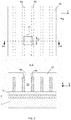
- a mask layer 10 is deposited on the wafer, and patterned so that an opening 11 is formed in the mask layer.
- the mask layer 10 may be obtained by a multilayer stack known as such in the art, and consisting of a spin-on-carbon layer, a spin-on glass layer, and a resist layer.
- the dimensions and position of the opening 11 are such that the opening overlaps the opposite edges of two adjacent mandrel lines 4a and 4b in the Y-direction, while extending over a given distance D in the X-direction. Only one opening 11 is shown in the example, but multiple openings may be present depending on the required pattern. One opening could overlap more than two adjacent mandrel lines 4.
- the overlap in the Y-direction means that the opening 11 is over-dimensioned with respect to the spacing between the adjacent mandrel lines 4a and 4b.
- An etch process is then applied that removes the SiN layer 3 selectively with respect to the mandrel lines 4 and the mask layer 10, after which the mask layer 10 is stripped, see Figure 3a .
- This may be a reactive ion etch process known per se in the art. Due to the over-dimensioned opening 11, the etch process is self-aligned in the Y-direction, i.e. the opening 12 that is etched in the SiN layer 3 aligns to the sides of the mandrel lines 4a and 4b.
- the SiN layer 3 may be etched so that it has vertical sidewalls 13a and 13b as shown in the detail in Figure 3b , to thereby create an essentially rectangular opening with size D in this X-direction.
- This etch with perfectly vertical sidewalls is achievable but it is not the standard case, as the sidewalls of the opening 11 in the mask layer 10 are usually slanted inward, and this slope is transferred to the opening 12 in the SiN layer 3.
- This slanted angle is however not disadvantageous for the present invention, as long as the slanting angle is not too pronounced, as will be explained later in this description.
- vertical sidewalls of the opening 12 are assumed.
- a layer 14 of the spacer material is deposited conformally, see Figure 4a .
- the spacer material may be silicon dioxide, deposited at a thickness configured so that the gap between two adjacent vertical spacer layers on the sidewalls of the mandrel lines is approximately the same in thickness as the mandrel lines. For example, if the mandrel lines are 8 nm wide and spaced apart about 24nm, the spacer thickness may be about 8 nm as well.
- the process used for depositing the spacer material may be any process known in the art for this purpose, such as atomic layer deposition (ALD).
- ALD atomic layer deposition
- the spacer material now also lines the sidewalls and bottom of the opening, as shown in the detail section in Figure 4b .
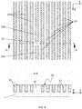
- the spacer material 14 is etched back in the direction perpendicular to the wafer, see Figure 5a , until the top of the mandrel lines 4 and the SiN layer 3 in between the mandrel lines 4 is exposed, thereby creating effective spacers 19 on the vertical sidewalls of the mandrel lines 4.
- This may be realized by a plasma etch process as known per se in the art, that protects the vertical surfaces of the spacers while etching away the horizontal portions of the spacer material.
- the result is that a central area 15 of the TiN hardmask layer 2 becomes exposed in the centre of the bottom of the opening 12, surrounded on all sides by spacer material.
- FIG. 5a and the detail section in Figure 5b illustrate that in the Y-direction, the TiN area 15 is located between two high spacers 19a and 19b (having the height of the mandrel lines), and in the X-direction the TiN area 15 is located between two low spacers (having the height of the SiN layer) 16a and 16b.
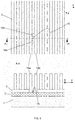
- the mandrel lines 4 are then removed selectively with respect to the spacers 19 and 16a, 16b, see Figure 6 .
- ASD area selective deposition
- a layer 20 of ruthenium is deposited only on the TiN area 15, see Figure 7 .
- ASD is a process known as such and applied already in similar processes. The parameters used in these known processes can be applied also in this particular step of the method of the invention illustrated in Figure 7 .
- the ruthenium is a blocking material for the subsequent patterning of the TiN hardmask 2.
- Other materials that may be used instead of Ru are titanium oxide or platinum.
- the blocking material may also be applied by methods other than ASD, such as by chemical vapour deposition of a conformal layer, followed by a patterning step.
- the etching of the TiN hardmask 2 takes place, using the spacers 19, 16a, 16b and the Ru-block 20 as a mask, followed by stripping the spacer material 19, the Ru block 20, and the SiN layer 3. Then the IMD layer 1 is etched in accordance with the Ti mask to form trenches 21 in this IMD layer 1.
- the trenches are formed everywhere except at the location of the Ru block, where a dielectric gap 22 is formed between two colinear trenches 21a and 21b.
- the colinear metal lines 23a and 23b are separated by the dielectric gap 22.
- the tip-to-tip spacing between the metal lines 23 can be much smaller compared to prior art methods. As shown in Figure 5 , this is because the spacers 16a and 16b are formed on the sidewalls of the opening 12, thereby shrinking the area 15 of exposed TiN. The dimensions of this area ultimately determine the dimensions of the Ru block 20 and thus of the tip-to-tip spacing, i.e. the width of the dielectric gap 22.
- the size D of the opening 12 in the X-direction is determined by the lithography used for producing the hardmask 10. With current technologies, this width can be reduced to the order of 20nm.
- the spacers 16a and 16b may be about 8nm wide, leaving a width of about 4nm for the area 15, and thus for the tip-to-tip spacing.
- tip to tip spacing can therefore be reduced significantly with respect to the best achievable values of about 18 nm of the present state of the art.
- the tip-to-tip spacing is lower than 10nm, or lower than 5nm.
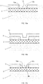
- the sides 13a and 13b of the opening 12 etched in the SiN layer 3 may be slightly slanted inward toward the middle of the opening, as a consequence of an inwardly slanted orientation of the sidewalls of the opening 11 in the mask layer 10.
- Figure 10a Figures 10b and 10c illustrate that the deposition of the spacer material 14 and the spacer etch-back are performed as described above, also in the case of the slanted sides 13a and 13b, and that this slanted orientation further reduces the width of the exposed TiN area 15 in the X-direction. Therefore, as long as the slanted orientation is not too pronounced, this is actually advantageous in minimizing the tip-to-tip spacing.
- the phenomenon of the slanted inner walls is a consequence of the fact that the etch process which defines the width of the dielectric gap 22 in the X-direction is a negative tone development process.
- self aligned block areas are defined by positive tone development processes, i.e. by creating a pillar instead of an opening at the location of the self-aligned block.
- the sides of the pillars may be slanted as well, but in this case they behave in the opposite way to the sides of the opening 12 in Figure 10a , i.e. the pillar is wider at the bottom then at the top, which counteracts any shrinking of the block dimension.
- the array of mandrel lines 4 is just one example of the 'sacrificial structure' referred to in appended claim 1.
- the invention is applicable to any sacrificial structure comprising two parallel sidewalls onto which spacers are deposited. This occurs for example also in the SALELE technique (self-aligned litho-etch litho-etch), wherein spacers are deposited on the inner walls of elongate openings formed in a sacrificial layer.
- the method described above can be applied as such on this type of sacrificial structure for producing two colinear conductive lines separated by a dielectric tip-to-tip gap, the lines being defined by the width between two spacers deposited on two mutually facing inner walls of an elongate opening in the sacrificial layer.
Landscapes
- Internal Circuitry In Semiconductor Integrated Circuit Devices (AREA)
- Physics & Mathematics (AREA)
- Geometry (AREA)
Abstract
Description
- The present invention is related to semiconductor processing, in particular to the fabrication of a dense pattern of electrically conductive lines, as applied in the back end of line part of a chip manufacturing process.
- The back end of line (BEOL) refers to the interconnect structure of a semiconductor chip and to the process of fabricating this structure. The BEOL structure comprises multiple levels of electrical conductors, connected together through interconnect vias. The continuing trend in terms of scale reduction has led to the application of specific techniques for the production of a dense array of nano-scaled metal lines in the BEOL. In particular the use of self-aligned patterning techniques has been introduced. One challenge is the scaling of the tip-to-tip space between two colinear metal lines, which is typically produced using a self-aligned block approach. However, whereas the pitch between parallel metal lines has been reduced to about 16nm using dual and quadruple self-aligned patterning techniques, there are currently no reliable techniques for reducing the tip-to-tip spacing to values lower than about 18nm. The tip-to-tip spacing is therefore disproportionately high with respect to the linewidths and pitch, and a reduction of this spacing is desirable in terms of obtaining a more efficient utilisation of the available chip surface.
- The invention aims to provide a solution to the problem described in the previous paragraph. This aim is achieved by the method according to the appended claims.
- The invention is related to a method for producing electrically conductive lines such as lines in the BEOL, wherein spacers are deposited on a sacrificial structure present on a stack of layers, comprising a hardmask layer on top of a dielectric layer into which the lines are to be embedded, and an intermediate layer on top of the hardmask layer. The sacrificial structure may be an array of parallel mandrel lines as known from self-aligned multiple patterning techniques. A self-aligned litho-etch step is then performed to create an opening in the intermediate layer, the opening being self-aligned to the space between two adjacent sidewalls of the sacrificial structure. The opening is formed prior to the deposition of spacers on the sacrificial structure, so that spacers are also formed on the transverse sidewalls of the opening, i.e. perpendicular to the spacers on the walls of the sacrificial structure. A blocking material is provided in the area of the bottom of the opening that is surrounded on all sides by spacers, thereby creating a block with a reduced size, compared to prior art techniques. The transfer of the spacer and block pattern to the hardmask layer allows to create colinear conductive lines with a reduced tip-to-tip spacing compared to the prior art.
- The invention is in particular related to a method for producing electrically conductive lines on a planar substrate, embedded in a dielectric material, wherein at least two colinear lines are separated by a dielectric gap between the tips of said two lines, the method comprising the following steps :
- producing a mask layer on a layer of said dielectric material formed on the substrate,
- producing an intermediate layer on top of and in contact with the mask layer,
- producing a sacrificial structure on the intermediate layer, the sacrificial structure comprising at least two parallel and mutually facing sidewalls of the structure with an elongate open area between said sidewalls, the open area extending in the X-direction of an orthogonal X-Y axis system in a plane parallel to the substrate,
- by a lithography and etch process, producing an essentially rectangular opening in the intermediate layer, thereby locally exposing the mask layer, wherein
- ∘ the size of the opening in the Y-direction is self-aligned relative to the two parallel sidewalls,
- ∘ the sizeof the opening in the X-direction is defined by a mask pattern applied in the lithography and etch process,
- depositing a layer of spacer material conformally on the sacrificial structure and on the bottom and sidewalls of the opening,
- etching back the spacer material so as to expose the top of the sacrificial structure, thereby creating :
- ∘ Two high spacers extending in the X-direction on the two parallel sidewalls,
- ∘ Two low spacers extending in the Y-direction on the two sidewalls of the opening extending in said Y-direction, wherein the mask layer is exposed in an area of the bottom of the opening, said area being surrounded by the two low spacers and by the two high spacers,
- Removing the sacrificial structure selectively with respect to the spacers,
- Depositing a blocking material on the exposed area of the mask layer,
- Using the spacers and the blocking material as a mask for patterning the intermediate layer and the mask layer, thereby creating a patterned mask on the layer of dielectric material,
- Etching trenches in the layer of dielectric material, in accordance with the patterned mask,
- Filling the trenches with an electrically conductive material and planarizing said material, thereby obtaining two colinear conductive lines separated by a dielectric gap at the location of the blocking material.
- According to an embodiment, the sacrificial structure is an array of mutually parallel mandrel lines, and wherein the two parallel sidewalls of the sacrificial structure are the mutually facing sidewalls of two adjacent mandrel lines.
- According to an embodiment, the sidewalls of the opening in the intermediate layer, extending in the Y-direction are slanted inward toward the middle of the opening, so that the width in the X-direction of the exposed area of the mask layer is reduced compared to a case wherein said sidewalls of the opening are vertical.
- The mask layer may be a titanium nitride layer and the intermediate layer may be a layer of silicon nitride.
- According to various embodiments, the width of the dielectric gap in the X-direction is lower than 18 nm, or lower than 10 nm or lower than 5 nm.
-
-
Figure 1 shows a plane view and a section view of a portion of a substrate onto which the method of the invention may be applied. -
Figures 2 to 9 illustrate the consecutive method steps applied to the substrate shown inFigure 1 , in accordance with an embodiment of the invention. -
Figures 10a to 10c illustrate how a slanted angle of the sidewalls of an opening produced during the method of the invention can further shrink the tip-to-tip spacing. - The invention will be described with reference to the drawings, and with reference to specific materials for the layers and structures shown therein. These materials are stated by way of example, and do not form a limitation to the scope of the invention. A
layer 1 of a dielectric material is shown inFigure 1 . This may be a layer of so-called inter-metal dielectric present on a semiconductor wafer (not shown) onto which a front end of line (FEOL) process has been performed, fabricating active devices such as transistors and diodes on the wafer. The IMD layer may be a layer of silicon dioxide. As well-known to the skilled person, the BEOL process consists of the consecutive deposition and patterning of IMD layers into which via openings and trenches are etched and subsequently filled with a conductive material, to thereby form a multi-level interconnect structure. The method of the invention is applicable to the formation of any one of these levels, in particular to the formation of a level comprising a dense array of nano-scaled parallel conductors. - A titanium nitride (TiN)
hardmask layer 2 is present on top of and in contact with theIMD layer 1. Thehardmask 2 will be patterned by the method steps described hereafter, in order to form a pattern that is to be transferred by etching into theIMD layer 1. On top of and in contact with theTiN layer 2 is alayer 3 of silicon nitride, hereafter referred to as the 'SiN' layer for conciseness, even though the chemical compound forming this layer is preferably Si3N4. Thislayer 3 is what is referred to as the 'intermediate layer' in the appended claims. Both theTiN layer 2 and theSiN layer 3 may have thicknesses between 5 nm and 30 nm. Suitable techniques for producing these TiN and SiN layers are chemical vapour deposition (CVD) and Atomic Layer Deposition (ALD). On theSiN layer 3, an array of parallel fin-shaped structures 4 is present, referred to hereafter asmandrel lines 4, formed of amorphous silicon. Themandrel lines 4 extend in the X-direction of an orthogonal X-Y axis system in a plane parallel to the wafer surface. Themandrel lines 4 are formed according to any known method for self-aligned multiple patterning, such as SADP (self-aligned double patterning) or SAQP (self-aligned quadruple patterning). The dimensions of the structure are in the order of nanometres. For example, the width of themandrel lines 4 may be about 8 nm. Themandrel lines 4 may be produced by a lithography and etch process in the case of SADP, and in the case of SAQP by depositing spacers on a set of initial wider mandrel lines and transferring the spacer pattern to an underlying layer to create the mandrel lines shown inFigure 1 . Process details as known from SADP and SAQP technologies may be applied. - As also known in the art, the mandrel structure serves as a support for the formation of spacers (second spacers in the case of SAQP) on the sides of the
mandrel lines 4, followed by the removal of the mandrel material, thereby creating spacer lines at a reduced pitch compared to the mandrel lines. The spacers subsequently define the pattern that is transferred to theTiN hardmask 2 and ultimately to theIMD layer 1. However, in order to produce two conductive lines in theIMD layer 1 extending along the same linear direction and interrupted by a dielectric gap that isolates the tips of the lines from each other, a blocking material needs to be applied locally on theTiN mask 2. According to what is generally referred to as the 'self-aligned block' technology, this blocking material is applied by a self-aligned etch process applied after the spacer deposition. - The present invention differs from the prior art methodology by performing a number of steps related to the self-aligned block, before the spacer deposition. The details are explained with reference to
Figures 2 to 9 . As shown inFigure 2 , amask layer 10 is deposited on the wafer, and patterned so that anopening 11 is formed in the mask layer. Themask layer 10 may be obtained by a multilayer stack known as such in the art, and consisting of a spin-on-carbon layer, a spin-on glass layer, and a resist layer. The dimensions and position of theopening 11 are such that the opening overlaps the opposite edges of twoadjacent mandrel lines opening 11 is shown in the example, but multiple openings may be present depending on the required pattern. One opening could overlap more than twoadjacent mandrel lines 4. - The overlap in the Y-direction means that the
opening 11 is over-dimensioned with respect to the spacing between theadjacent mandrel lines SiN layer 3 selectively with respect to themandrel lines 4 and themask layer 10, after which themask layer 10 is stripped, seeFigure 3a . This may be a reactive ion etch process known per se in the art. Due to theover-dimensioned opening 11, the etch process is self-aligned in the Y-direction, i.e. theopening 12 that is etched in theSiN layer 3 aligns to the sides of themandrel lines SiN layer 3 may be etched so that it hasvertical sidewalls Figure 3b , to thereby create an essentially rectangular opening with size D in this X-direction. This etch with perfectly vertical sidewalls is achievable but it is not the standard case, as the sidewalls of theopening 11 in themask layer 10 are usually slanted inward, and this slope is transferred to theopening 12 in theSiN layer 3. This slanted angle is however not disadvantageous for the present invention, as long as the slanting angle is not too pronounced, as will be explained later in this description. For the sake of explaining the main characteristics of the invention however, vertical sidewalls of theopening 12 are assumed. - After this etch process, a
layer 14 of the spacer material is deposited conformally, seeFigure 4a . The spacer material may be silicon dioxide, deposited at a thickness configured so that the gap between two adjacent vertical spacer layers on the sidewalls of the mandrel lines is approximately the same in thickness as the mandrel lines. For example, if the mandrel lines are 8 nm wide and spaced apart about 24nm, the spacer thickness may be about 8 nm as well. The process used for depositing the spacer material may be any process known in the art for this purpose, such as atomic layer deposition (ALD). In theopening 12, the spacer material now also lines the sidewalls and bottom of the opening, as shown in the detail section inFigure 4b . - The
spacer material 14 is etched back in the direction perpendicular to the wafer, seeFigure 5a , until the top of themandrel lines 4 and theSiN layer 3 in between themandrel lines 4 is exposed, thereby creatingeffective spacers 19 on the vertical sidewalls of the mandrel lines 4. This may be realized by a plasma etch process as known per se in the art, that protects the vertical surfaces of the spacers while etching away the horizontal portions of the spacer material. The result is that acentral area 15 of theTiN hardmask layer 2 becomes exposed in the centre of the bottom of theopening 12, surrounded on all sides by spacer material.Figure 5a and the detail section inFigure 5b illustrate that in the Y-direction, theTiN area 15 is located between twohigh spacers TiN area 15 is located between two low spacers (having the height of the SiN layer) 16a and 16b. - The
mandrel lines 4 are then removed selectively with respect to thespacers Figure 6 . By a process known as area selective deposition (ASD), alayer 20 of ruthenium is deposited only on theTiN area 15, seeFigure 7 . ASD is a process known as such and applied already in similar processes. The parameters used in these known processes can be applied also in this particular step of the method of the invention illustrated inFigure 7 . The ruthenium is a blocking material for the subsequent patterning of theTiN hardmask 2. Other materials that may be used instead of Ru are titanium oxide or platinum. The blocking material may also be applied by methods other than ASD, such as by chemical vapour deposition of a conformal layer, followed by a patterning step. - As illustrated in
Figure 8 , the etching of theTiN hardmask 2 takes place, using thespacers block 20 as a mask, followed by stripping thespacer material 19, theRu block 20, and theSiN layer 3. Then theIMD layer 1 is etched in accordance with the Ti mask to formtrenches 21 in thisIMD layer 1. The trenches are formed everywhere except at the location of the Ru block, where adielectric gap 22 is formed between twocolinear trenches - This is followed by the step of filling the
trenches 21 with conductive material, preferably metal, seeFigure 9 , and planarizing the wafer, to form a set ofparallel metal lines 23 embedded in theIMD material 1, and having a levelupper surface 24, onto which possibly a further IMD layer may be applied. Thecolinear metal lines dielectric gap 22. - By forming the self-aligned
opening 12 before the spacer deposition, the tip-to-tip spacing between themetal lines 23 can be much smaller compared to prior art methods. As shown inFigure 5 , this is because thespacers opening 12, thereby shrinking thearea 15 of exposed TiN. The dimensions of this area ultimately determine the dimensions of theRu block 20 and thus of the tip-to-tip spacing, i.e. the width of thedielectric gap 22. The size D of theopening 12 in the X-direction is determined by the lithography used for producing thehardmask 10. With current technologies, this width can be reduced to the order of 20nm. Thespacers area 15, and thus for the tip-to-tip spacing. In general, tip to tip spacing can therefore be reduced significantly with respect to the best achievable values of about 18 nm of the present state of the art. According to preferred embodiments, the tip-to-tip spacing is lower than 10nm, or lower than 5nm. - As stated above with reference to
Figure 3b , thesides opening 12 etched in theSiN layer 3 may be slightly slanted inward toward the middle of the opening, as a consequence of an inwardly slanted orientation of the sidewalls of theopening 11 in themask layer 10. This situation is illustrated inFigure 10a. Figures 10b and 10c illustrate that the deposition of thespacer material 14 and the spacer etch-back are performed as described above, also in the case of the slantedsides TiN area 15 in the X-direction. Therefore, as long as the slanted orientation is not too pronounced, this is actually advantageous in minimizing the tip-to-tip spacing. - The phenomenon of the slanted inner walls is a consequence of the fact that the etch process which defines the width of the
dielectric gap 22 in the X-direction is a negative tone development process. In many prior art processes, self aligned block areas are defined by positive tone development processes, i.e. by creating a pillar instead of an opening at the location of the self-aligned block. The sides of the pillars may be slanted as well, but in this case they behave in the opposite way to the sides of theopening 12 inFigure 10a , i.e. the pillar is wider at the bottom then at the top, which counteracts any shrinking of the block dimension. - The array of
mandrel lines 4 is just one example of the 'sacrificial structure' referred to in appendedclaim 1. The invention is applicable to any sacrificial structure comprising two parallel sidewalls onto which spacers are deposited. This occurs for example also in the SALELE technique (self-aligned litho-etch litho-etch), wherein spacers are deposited on the inner walls of elongate openings formed in a sacrificial layer. The method described above can be applied as such on this type of sacrificial structure for producing two colinear conductive lines separated by a dielectric tip-to-tip gap, the lines being defined by the width between two spacers deposited on two mutually facing inner walls of an elongate opening in the sacrificial layer. - While the invention has been illustrated and described in detail in the drawings and foregoing description, such illustration and description are to be considered illustrative or exemplary and not restrictive. Other variations to the disclosed embodiments can be understood and effected by those skilled in the art in practicing the claimed invention, from a study of the drawings, the disclosure and the appended claims. In the claims, the word "comprising" does not exclude other elements or steps, and the indefinite article "a" or "an" does not exclude a plurality. The mere fact that certain measures are recited in mutually different dependent claims does not indicate that a combination of these measures cannot be used to advantage. Any reference signs in the claims should not be construed as limiting the scope.
Claims (7)
- A method for producing electrically conductive lines (23) on a planar substrate, embedded in a dielectric material (1), wherein at least two colinear lines (23a,23b) are separated by a dielectric gap (22) between the tips of said two lines, the method comprising the following steps :- producing a mask layer (2) on a layer of said dielectric material (1) formed on the substrate,- producing an intermediate layer (3) on top of and in contact with the mask layer (2),- producing a sacrificial structure (4) on the intermediate layer, the sacrificial structure comprising at least two parallel and mutually facing sidewalls of the structure with an elongate open area between said sidewalls, the open area extending in the X-direction of an orthogonal X-Y axis system in a plane parallel to the substrate,- by a lithography and etch process, producing an essentially rectangular opening (12) in the intermediate layer (3), thereby locally exposing the mask layer (2), wherein∘ the size of the opening (12) in the Y-direction is self-aligned relative to the two parallel sidewalls,∘ the size (D) of the opening (12) in the X-direction is defined by a mask pattern applied in the lithography and etch process,- depositing a layer of spacer material (14) conformally on the sacrificial structure (4) and on the bottom and sidewalls of the opening (12),- etching back the spacer material so as to expose the top of the sacrificial structure, thereby creating :∘ Two high spacers (19a, 19b) extending in the X-direction on the two parallel sidewalls,∘ Two low spacers (16a, 16b) extending in the Y-direction on the two sidewalls of the opening (12) extending in said Y-direction, wherein the mask layer (2) is exposed in an area (15) of the bottom of the opening (12), said area (15) being surrounded by the two low spacers (16a,16b) and by the two high spacers (19a,19b),- Removing the sacrificial structure (4) selectively with respect to the spacers (19a, 19b),- Depositing a blocking material (20) on the exposed area (15) of the mask layer (2),- Using the spacers (19a, 19b, 16a, 16b) and the blocking material (20) as a mask for patterning the intermediate layer (3) and the mask layer (2), thereby creating a patterned mask on the layer of dielectric material (1),- Etching trenches (21a,21b) in the layer of dielectric material (1), in accordance with the patterned mask,- Filling the trenches (21a,21b) with an electrically conductive material and planarizing said material, thereby obtaining two colinear conductive lines (23a,23b) separated by a dielectric gap (22) at the location of the blocking material (20).
- The method according to claim 1, wherein the sacrificial structure is an array of mutually parallel mandrel lines (4), and wherein the two parallel sidewalls of the sacrificial structure are the mutually facing sidewalls of two adjacent mandrel lines (4a,4b).
- The method according to claim 1 or 2, wherein the sidewalls (13a, 13b) of the opening (12) in the intermediate layer (3), extending in the Y-direction are slanted inward toward the middle of the opening (12), so that the width in the X-direction of the exposed area (15) of the mask layer (2) is reduced compared to a case wherein said sidewalls (13a, 13b) of the opening (12) are vertical.
- The method according to any one of the preceding claims, wherein the mask layer (2) is a titanium nitride layer and the intermediate layer (3) is a layer of silicon nitride.
- The method according to any one of the preceding claims, wherein the width of the dielectric gap (22) in the X-direction is lower than 18 nm.
- The method according to any one of claims 1 to 4, wherein the width of the dielectric gap (22) in the X-direction is lower than 10 nm.
- The method according to any one of claims 1 to 4, wherein the width of the dielectric gap (22) in the X-direction is lower than 5 nm.
Priority Applications (2)
| Application Number | Priority Date | Filing Date | Title |
|---|---|---|---|
| EP19217971.1A EP3840034B1 (en) | 2019-12-19 | 2019-12-19 | Method for producing nanoscaled electrically conductive lines for semiconductor devices |
| US17/081,337 US11264271B2 (en) | 2019-12-19 | 2020-10-27 | Semiconductor fabrication method for producing nano-scaled electrically conductive lines |
Applications Claiming Priority (1)
| Application Number | Priority Date | Filing Date | Title |
|---|---|---|---|
| EP19217971.1A EP3840034B1 (en) | 2019-12-19 | 2019-12-19 | Method for producing nanoscaled electrically conductive lines for semiconductor devices |
Publications (2)
| Publication Number | Publication Date |
|---|---|
| EP3840034A1 true EP3840034A1 (en) | 2021-06-23 |
| EP3840034B1 EP3840034B1 (en) | 2022-06-15 |
Family
ID=68965868
Family Applications (1)
| Application Number | Title | Priority Date | Filing Date |
|---|---|---|---|
| EP19217971.1A Active EP3840034B1 (en) | 2019-12-19 | 2019-12-19 | Method for producing nanoscaled electrically conductive lines for semiconductor devices |
Country Status (2)
| Country | Link |
|---|---|
| US (1) | US11264271B2 (en) |
| EP (1) | EP3840034B1 (en) |
Families Citing this family (1)
| Publication number | Priority date | Publication date | Assignee | Title |
|---|---|---|---|---|
| KR20240025916A (en) | 2022-08-19 | 2024-02-27 | 삼성전자주식회사 | Method of fabraicating semiconductor device |
Citations (3)
| Publication number | Priority date | Publication date | Assignee | Title |
|---|---|---|---|---|
| US9786545B1 (en) * | 2016-09-21 | 2017-10-10 | Globalfoundries Inc. | Method of forming ANA regions in an integrated circuit |
| US9818641B1 (en) * | 2016-09-21 | 2017-11-14 | Globalfoundries Inc. | Apparatus and method of forming self-aligned cuts in mandrel and a non-mandrel lines of an array of metal lines |
| US9953834B1 (en) * | 2017-10-03 | 2018-04-24 | Globalfoundries Inc. | Method of making self-aligned continuity cuts in mandrel and non-mandrel metal lines |
Family Cites Families (20)
| Publication number | Priority date | Publication date | Assignee | Title |
|---|---|---|---|---|
| US10366890B2 (en) | 2016-05-23 | 2019-07-30 | Tokyo Electron Limited | Method for patterning a substrate using a layer with multiple materials |
| US9966338B1 (en) * | 2017-04-18 | 2018-05-08 | Globalfoundries Inc. | Pre-spacer self-aligned cut formation |
| US10249496B2 (en) * | 2017-05-05 | 2019-04-02 | Globalfoundries Inc. | Narrowed feature formation during a double patterning process |
| US10199270B2 (en) * | 2017-05-25 | 2019-02-05 | Globalfoundries Inc. | Multi-directional self-aligned multiple patterning |
| US10319626B1 (en) * | 2017-12-07 | 2019-06-11 | Globalfoundries Inc. | Interconnects with cuts formed by block patterning |
| US11127594B2 (en) | 2017-12-19 | 2021-09-21 | Tokyo Electron Limited | Manufacturing methods for mandrel pull from spacers for multi-color patterning |
| US10755969B2 (en) * | 2018-01-01 | 2020-08-25 | International Business Machines Corporation | Multi-patterning techniques for fabricating an array of metal lines with different widths |
| US10446395B1 (en) * | 2018-04-11 | 2019-10-15 | Globalfoundries Inc. | Self-aligned multiple patterning processes with layered mandrels |
| US10629436B2 (en) * | 2018-04-12 | 2020-04-21 | International Business Machines Corporation | Spacer image transfer with double mandrel |
| US10395926B1 (en) * | 2018-04-17 | 2019-08-27 | Globalfoundries Inc. | Multiple patterning with mandrel cuts formed using a block mask |
| US10784195B2 (en) * | 2018-04-23 | 2020-09-22 | Globalfoundries Inc. | Electrical fuse formation during a multiple patterning process |
| US10692812B2 (en) * | 2018-05-15 | 2020-06-23 | Globalfoundries Inc. | Interconnects with variable space mandrel cuts formed by block patterning |
| US10490447B1 (en) * | 2018-05-25 | 2019-11-26 | International Business Machines Corporation | Airgap formation in BEOL interconnect structure using sidewall image transfer |
| US10192780B1 (en) * | 2018-05-29 | 2019-01-29 | Globalfoundries Inc. | Self-aligned multiple patterning processes using bi-layer mandrels and cuts formed with block masks |
| US10651046B2 (en) * | 2018-10-08 | 2020-05-12 | Globalfoundries Inc. | Multiple patterning with late lithographically-defined mandrel cuts |
| US11417525B2 (en) * | 2018-10-08 | 2022-08-16 | Globalfoundries U.S. Inc. | Multiple patterning with mandrel cuts defined by block masks |
| US10784119B2 (en) * | 2018-10-08 | 2020-09-22 | Globalfoundries Inc. | Multiple patterning with lithographically-defined cuts |
| US10825726B2 (en) * | 2018-10-16 | 2020-11-03 | International Business Machines Corporation | Metal spacer self aligned multi-patterning integration |
| US11061315B2 (en) * | 2018-11-15 | 2021-07-13 | Globalfoundries U.S. Inc. | Hybrid optical and EUV lithography |
| US11574811B2 (en) * | 2019-09-23 | 2023-02-07 | International Business Machines Corporation | Tight pitch patterning |
-
2019
- 2019-12-19 EP EP19217971.1A patent/EP3840034B1/en active Active
-
2020
- 2020-10-27 US US17/081,337 patent/US11264271B2/en active Active
Patent Citations (3)
| Publication number | Priority date | Publication date | Assignee | Title |
|---|---|---|---|---|
| US9786545B1 (en) * | 2016-09-21 | 2017-10-10 | Globalfoundries Inc. | Method of forming ANA regions in an integrated circuit |
| US9818641B1 (en) * | 2016-09-21 | 2017-11-14 | Globalfoundries Inc. | Apparatus and method of forming self-aligned cuts in mandrel and a non-mandrel lines of an array of metal lines |
| US9953834B1 (en) * | 2017-10-03 | 2018-04-24 | Globalfoundries Inc. | Method of making self-aligned continuity cuts in mandrel and non-mandrel metal lines |
Also Published As
| Publication number | Publication date |
|---|---|
| US20210193512A1 (en) | 2021-06-24 |
| US11264271B2 (en) | 2022-03-01 |
| EP3840034B1 (en) | 2022-06-15 |
Similar Documents
| Publication | Publication Date | Title |
|---|---|---|
| US11361988B2 (en) | Staircase formation in three-dimensional memory device | |
| US11114439B2 (en) | Multi-division 3D NAND memory device | |
| US20130193489A1 (en) | Integrated circuits including copper local interconnects and methods for the manufacture thereof | |
| US8962432B2 (en) | Semiconductor device with self aligned end-to-end conductive line structure and method for forming the same | |
| TWI742350B (en) | Self-aligned multiple patterning processes with layered mandrels | |
| TWI660424B (en) | Method of forming ana regions in an integrated circuit | |
| US10217696B2 (en) | Non-bridging contact via structures in proximity | |
| TW201814829A (en) | Apparatus and method for forming a self-aligning slit in a non-center of an array of metal wires | |
| CN111403397A (en) | 3D NAND memory and manufacturing method thereof | |
| EP3188225A2 (en) | Semiconductor device with local interconnect structure and manufacturing method thereof | |
| EP3840034B1 (en) | Method for producing nanoscaled electrically conductive lines for semiconductor devices | |
| US11456252B2 (en) | Semiconductor device having symmetric conductive interconnection patterns | |
| TWI223380B (en) | Semiconductor device and method of fabricating the same | |
| CN102280406B (en) | Manufacture the method for semiconductor device | |
| KR100597594B1 (en) | Method of forming contact plug of semiconductor device | |
| EP3817038A1 (en) | A method for producing self-aligned gate and source/drain via connections for contacting a fet transistor | |
| EP3836198B1 (en) | A method for forming a via hole self-aligned with a metal block on a substrate | |
| WO2024137032A1 (en) | Self-aligned line-and-via structure and method of making the same | |
| CN118574408A (en) | Semiconductor structure and preparation method thereof |
Legal Events
| Date | Code | Title | Description |
|---|---|---|---|
| PUAI | Public reference made under article 153(3) epc to a published international application that has entered the european phase |
Free format text: ORIGINAL CODE: 0009012 |
|
| STAA | Information on the status of an ep patent application or granted ep patent |
Free format text: STATUS: THE APPLICATION HAS BEEN PUBLISHED |
|
| AK | Designated contracting states |
Kind code of ref document: A1 Designated state(s): AL AT BE BG CH CY CZ DE DK EE ES FI FR GB GR HR HU IE IS IT LI LT LU LV MC MK MT NL NO PL PT RO RS SE SI SK SM TR |
|
| STAA | Information on the status of an ep patent application or granted ep patent |
Free format text: STATUS: REQUEST FOR EXAMINATION WAS MADE |
|
| 17P | Request for examination filed |
Effective date: 20211221 |
|
| RBV | Designated contracting states (corrected) |
Designated state(s): AL AT BE BG CH CY CZ DE DK EE ES FI FR GB GR HR HU IE IS IT LI LT LU LV MC MK MT NL NO PL PT RO RS SE SI SK SM TR |
|
| GRAP | Despatch of communication of intention to grant a patent |
Free format text: ORIGINAL CODE: EPIDOSNIGR1 |
|
| STAA | Information on the status of an ep patent application or granted ep patent |
Free format text: STATUS: GRANT OF PATENT IS INTENDED |
|
| RIC1 | Information provided on ipc code assigned before grant |
Ipc: H01L 21/768 20060101AFI20220322BHEP |
|
| GRAS | Grant fee paid |
Free format text: ORIGINAL CODE: EPIDOSNIGR3 |
|
| INTG | Intention to grant announced |
Effective date: 20220412 |
|
| GRAA | (expected) grant |
Free format text: ORIGINAL CODE: 0009210 |
|
| STAA | Information on the status of an ep patent application or granted ep patent |
Free format text: STATUS: THE PATENT HAS BEEN GRANTED |
|
| AK | Designated contracting states |
Kind code of ref document: B1 Designated state(s): AL AT BE BG CH CY CZ DE DK EE ES FI FR GB GR HR HU IE IS IT LI LT LU LV MC MK MT NL NO PL PT RO RS SE SI SK SM TR |
|
| REG | Reference to a national code |
Ref country code: CH Ref legal event code: EP Ref country code: GB Ref legal event code: FG4D |
|
| REG | Reference to a national code |
Ref country code: IE Ref legal event code: FG4D |
|
| REG | Reference to a national code |
Ref country code: DE Ref legal event code: R096 Ref document number: 602019015885 Country of ref document: DE |
|
| REG | Reference to a national code |
Ref country code: AT Ref legal event code: REF Ref document number: 1498891 Country of ref document: AT Kind code of ref document: T Effective date: 20220715 |
|
| REG | Reference to a national code |
Ref country code: LT Ref legal event code: MG9D |
|
| REG | Reference to a national code |
Ref country code: NL Ref legal event code: MP Effective date: 20220615 |
|
| PG25 | Lapsed in a contracting state [announced via postgrant information from national office to epo] |
Ref country code: SE Free format text: LAPSE BECAUSE OF FAILURE TO SUBMIT A TRANSLATION OF THE DESCRIPTION OR TO PAY THE FEE WITHIN THE PRESCRIBED TIME-LIMIT Effective date: 20220615 Ref country code: NO Free format text: LAPSE BECAUSE OF FAILURE TO SUBMIT A TRANSLATION OF THE DESCRIPTION OR TO PAY THE FEE WITHIN THE PRESCRIBED TIME-LIMIT Effective date: 20220915 Ref country code: LT Free format text: LAPSE BECAUSE OF FAILURE TO SUBMIT A TRANSLATION OF THE DESCRIPTION OR TO PAY THE FEE WITHIN THE PRESCRIBED TIME-LIMIT Effective date: 20220615 Ref country code: HR Free format text: LAPSE BECAUSE OF FAILURE TO SUBMIT A TRANSLATION OF THE DESCRIPTION OR TO PAY THE FEE WITHIN THE PRESCRIBED TIME-LIMIT Effective date: 20220615 Ref country code: GR Free format text: LAPSE BECAUSE OF FAILURE TO SUBMIT A TRANSLATION OF THE DESCRIPTION OR TO PAY THE FEE WITHIN THE PRESCRIBED TIME-LIMIT Effective date: 20220916 Ref country code: FI Free format text: LAPSE BECAUSE OF FAILURE TO SUBMIT A TRANSLATION OF THE DESCRIPTION OR TO PAY THE FEE WITHIN THE PRESCRIBED TIME-LIMIT Effective date: 20220615 Ref country code: BG Free format text: LAPSE BECAUSE OF FAILURE TO SUBMIT A TRANSLATION OF THE DESCRIPTION OR TO PAY THE FEE WITHIN THE PRESCRIBED TIME-LIMIT Effective date: 20220915 |
|
| REG | Reference to a national code |
Ref country code: AT Ref legal event code: MK05 Ref document number: 1498891 Country of ref document: AT Kind code of ref document: T Effective date: 20220615 |
|
| PG25 | Lapsed in a contracting state [announced via postgrant information from national office to epo] |
Ref country code: RS Free format text: LAPSE BECAUSE OF FAILURE TO SUBMIT A TRANSLATION OF THE DESCRIPTION OR TO PAY THE FEE WITHIN THE PRESCRIBED TIME-LIMIT Effective date: 20220615 Ref country code: LV Free format text: LAPSE BECAUSE OF FAILURE TO SUBMIT A TRANSLATION OF THE DESCRIPTION OR TO PAY THE FEE WITHIN THE PRESCRIBED TIME-LIMIT Effective date: 20220615 |
|
| PG25 | Lapsed in a contracting state [announced via postgrant information from national office to epo] |
Ref country code: NL Free format text: LAPSE BECAUSE OF FAILURE TO SUBMIT A TRANSLATION OF THE DESCRIPTION OR TO PAY THE FEE WITHIN THE PRESCRIBED TIME-LIMIT Effective date: 20220615 |
|
| PG25 | Lapsed in a contracting state [announced via postgrant information from national office to epo] |
Ref country code: SM Free format text: LAPSE BECAUSE OF FAILURE TO SUBMIT A TRANSLATION OF THE DESCRIPTION OR TO PAY THE FEE WITHIN THE PRESCRIBED TIME-LIMIT Effective date: 20220615 Ref country code: SK Free format text: LAPSE BECAUSE OF FAILURE TO SUBMIT A TRANSLATION OF THE DESCRIPTION OR TO PAY THE FEE WITHIN THE PRESCRIBED TIME-LIMIT Effective date: 20220615 Ref country code: RO Free format text: LAPSE BECAUSE OF FAILURE TO SUBMIT A TRANSLATION OF THE DESCRIPTION OR TO PAY THE FEE WITHIN THE PRESCRIBED TIME-LIMIT Effective date: 20220615 Ref country code: PT Free format text: LAPSE BECAUSE OF FAILURE TO SUBMIT A TRANSLATION OF THE DESCRIPTION OR TO PAY THE FEE WITHIN THE PRESCRIBED TIME-LIMIT Effective date: 20221017 Ref country code: ES Free format text: LAPSE BECAUSE OF FAILURE TO SUBMIT A TRANSLATION OF THE DESCRIPTION OR TO PAY THE FEE WITHIN THE PRESCRIBED TIME-LIMIT Effective date: 20220615 Ref country code: EE Free format text: LAPSE BECAUSE OF FAILURE TO SUBMIT A TRANSLATION OF THE DESCRIPTION OR TO PAY THE FEE WITHIN THE PRESCRIBED TIME-LIMIT Effective date: 20220615 Ref country code: CZ Free format text: LAPSE BECAUSE OF FAILURE TO SUBMIT A TRANSLATION OF THE DESCRIPTION OR TO PAY THE FEE WITHIN THE PRESCRIBED TIME-LIMIT Effective date: 20220615 Ref country code: AT Free format text: LAPSE BECAUSE OF FAILURE TO SUBMIT A TRANSLATION OF THE DESCRIPTION OR TO PAY THE FEE WITHIN THE PRESCRIBED TIME-LIMIT Effective date: 20220615 |
|
| PG25 | Lapsed in a contracting state [announced via postgrant information from national office to epo] |
Ref country code: PL Free format text: LAPSE BECAUSE OF FAILURE TO SUBMIT A TRANSLATION OF THE DESCRIPTION OR TO PAY THE FEE WITHIN THE PRESCRIBED TIME-LIMIT Effective date: 20220615 Ref country code: IS Free format text: LAPSE BECAUSE OF FAILURE TO SUBMIT A TRANSLATION OF THE DESCRIPTION OR TO PAY THE FEE WITHIN THE PRESCRIBED TIME-LIMIT Effective date: 20221015 |
|
| REG | Reference to a national code |
Ref country code: DE Ref legal event code: R097 Ref document number: 602019015885 Country of ref document: DE |
|
| PG25 | Lapsed in a contracting state [announced via postgrant information from national office to epo] |
Ref country code: AL Free format text: LAPSE BECAUSE OF FAILURE TO SUBMIT A TRANSLATION OF THE DESCRIPTION OR TO PAY THE FEE WITHIN THE PRESCRIBED TIME-LIMIT Effective date: 20220615 |
|
| PLBE | No opposition filed within time limit |
Free format text: ORIGINAL CODE: 0009261 |
|
| STAA | Information on the status of an ep patent application or granted ep patent |
Free format text: STATUS: NO OPPOSITION FILED WITHIN TIME LIMIT |
|
| PG25 | Lapsed in a contracting state [announced via postgrant information from national office to epo] |
Ref country code: DK Free format text: LAPSE BECAUSE OF FAILURE TO SUBMIT A TRANSLATION OF THE DESCRIPTION OR TO PAY THE FEE WITHIN THE PRESCRIBED TIME-LIMIT Effective date: 20220615 |
|
| 26N | No opposition filed |
Effective date: 20230316 |
|
| PG25 | Lapsed in a contracting state [announced via postgrant information from national office to epo] |
Ref country code: SI Free format text: LAPSE BECAUSE OF FAILURE TO SUBMIT A TRANSLATION OF THE DESCRIPTION OR TO PAY THE FEE WITHIN THE PRESCRIBED TIME-LIMIT Effective date: 20220615 |
|
| P01 | Opt-out of the competence of the unified patent court (upc) registered |
Effective date: 20230513 |
|
| REG | Reference to a national code |
Ref country code: CH Ref legal event code: PL |
|
| REG | Reference to a national code |
Ref country code: BE Ref legal event code: MM Effective date: 20221231 |
|
| PG25 | Lapsed in a contracting state [announced via postgrant information from national office to epo] |
Ref country code: LU Free format text: LAPSE BECAUSE OF NON-PAYMENT OF DUE FEES Effective date: 20221219 |
|
| PG25 | Lapsed in a contracting state [announced via postgrant information from national office to epo] |
Ref country code: LI Free format text: LAPSE BECAUSE OF NON-PAYMENT OF DUE FEES Effective date: 20221231 Ref country code: IE Free format text: LAPSE BECAUSE OF NON-PAYMENT OF DUE FEES Effective date: 20221219 Ref country code: CH Free format text: LAPSE BECAUSE OF NON-PAYMENT OF DUE FEES Effective date: 20221231 |
|
| PG25 | Lapsed in a contracting state [announced via postgrant information from national office to epo] |
Ref country code: FR Free format text: LAPSE BECAUSE OF NON-PAYMENT OF DUE FEES Effective date: 20221231 Ref country code: BE Free format text: LAPSE BECAUSE OF NON-PAYMENT OF DUE FEES Effective date: 20221231 |
|
| PG25 | Lapsed in a contracting state [announced via postgrant information from national office to epo] |
Ref country code: IT Free format text: LAPSE BECAUSE OF FAILURE TO SUBMIT A TRANSLATION OF THE DESCRIPTION OR TO PAY THE FEE WITHIN THE PRESCRIBED TIME-LIMIT Effective date: 20220615 |
|
| PG25 | Lapsed in a contracting state [announced via postgrant information from national office to epo] |
Ref country code: CY Free format text: LAPSE BECAUSE OF FAILURE TO SUBMIT A TRANSLATION OF THE DESCRIPTION OR TO PAY THE FEE WITHIN THE PRESCRIBED TIME-LIMIT Effective date: 20220615 |
|
| PG25 | Lapsed in a contracting state [announced via postgrant information from national office to epo] |
Ref country code: MK Free format text: LAPSE BECAUSE OF FAILURE TO SUBMIT A TRANSLATION OF THE DESCRIPTION OR TO PAY THE FEE WITHIN THE PRESCRIBED TIME-LIMIT Effective date: 20220615 Ref country code: HU Free format text: LAPSE BECAUSE OF FAILURE TO SUBMIT A TRANSLATION OF THE DESCRIPTION OR TO PAY THE FEE WITHIN THE PRESCRIBED TIME-LIMIT; INVALID AB INITIO Effective date: 20191219 |
|
| PG25 | Lapsed in a contracting state [announced via postgrant information from national office to epo] |
Ref country code: MC Free format text: LAPSE BECAUSE OF FAILURE TO SUBMIT A TRANSLATION OF THE DESCRIPTION OR TO PAY THE FEE WITHIN THE PRESCRIBED TIME-LIMIT Effective date: 20220615 |
|
| PG25 | Lapsed in a contracting state [announced via postgrant information from national office to epo] |
Ref country code: MC Free format text: LAPSE BECAUSE OF FAILURE TO SUBMIT A TRANSLATION OF THE DESCRIPTION OR TO PAY THE FEE WITHIN THE PRESCRIBED TIME-LIMIT Effective date: 20220615 |
|
| GBPC | Gb: european patent ceased through non-payment of renewal fee |
Effective date: 20231219 |
|
| PG25 | Lapsed in a contracting state [announced via postgrant information from national office to epo] |
Ref country code: MT Free format text: LAPSE BECAUSE OF FAILURE TO SUBMIT A TRANSLATION OF THE DESCRIPTION OR TO PAY THE FEE WITHIN THE PRESCRIBED TIME-LIMIT Effective date: 20220615 |
|
| PG25 | Lapsed in a contracting state [announced via postgrant information from national office to epo] |
Ref country code: GB Free format text: LAPSE BECAUSE OF NON-PAYMENT OF DUE FEES Effective date: 20231219 |
|
| PG25 | Lapsed in a contracting state [announced via postgrant information from national office to epo] |
Ref country code: GB Free format text: LAPSE BECAUSE OF NON-PAYMENT OF DUE FEES Effective date: 20231219 |
|
| PG25 | Lapsed in a contracting state [announced via postgrant information from national office to epo] |
Ref country code: BG Free format text: LAPSE BECAUSE OF FAILURE TO SUBMIT A TRANSLATION OF THE DESCRIPTION OR TO PAY THE FEE WITHIN THE PRESCRIBED TIME-LIMIT Effective date: 20220615 |
|
| PG25 | Lapsed in a contracting state [announced via postgrant information from national office to epo] |
Ref country code: BG Free format text: LAPSE BECAUSE OF FAILURE TO SUBMIT A TRANSLATION OF THE DESCRIPTION OR TO PAY THE FEE WITHIN THE PRESCRIBED TIME-LIMIT Effective date: 20220615 |
|
| REG | Reference to a national code |
Ref country code: DE Ref legal event code: R079 Ref document number: 602019015885 Country of ref document: DE Free format text: PREVIOUS MAIN CLASS: H01L0021768000 Ipc: H10W0020000000 |
|
| PG25 | Lapsed in a contracting state [announced via postgrant information from national office to epo] |
Ref country code: TR Free format text: LAPSE BECAUSE OF FAILURE TO SUBMIT A TRANSLATION OF THE DESCRIPTION OR TO PAY THE FEE WITHIN THE PRESCRIBED TIME-LIMIT Effective date: 20220615 |
|
| PGFP | Annual fee paid to national office [announced via postgrant information from national office to epo] |
Ref country code: DE Payment date: 20251126 Year of fee payment: 7 |