EP3838687A1 - Sensor for an impact detection and protection system and an impact detection and protection system for a vehicle - Google Patents
Sensor for an impact detection and protection system and an impact detection and protection system for a vehicle Download PDFInfo
- Publication number
- EP3838687A1 EP3838687A1 EP19216379.8A EP19216379A EP3838687A1 EP 3838687 A1 EP3838687 A1 EP 3838687A1 EP 19216379 A EP19216379 A EP 19216379A EP 3838687 A1 EP3838687 A1 EP 3838687A1
- Authority
- EP
- European Patent Office
- Prior art keywords
- sensor
- type
- sensor elements
- protection system
- elements
- Prior art date
- Legal status (The legal status is an assumption and is not a legal conclusion. Google has not performed a legal analysis and makes no representation as to the accuracy of the status listed.)
- Granted
Links
Images


Classifications
-
- G—PHYSICS
- G01—MEASURING; TESTING
- G01P—MEASURING LINEAR OR ANGULAR SPEED, ACCELERATION, DECELERATION, OR SHOCK; INDICATING PRESENCE, ABSENCE, OR DIRECTION, OF MOVEMENT
- G01P15/00—Measuring acceleration; Measuring deceleration; Measuring shock, i.e. sudden change of acceleration
- G01P15/02—Measuring acceleration; Measuring deceleration; Measuring shock, i.e. sudden change of acceleration by making use of inertia forces using solid seismic masses
- G01P15/08—Measuring acceleration; Measuring deceleration; Measuring shock, i.e. sudden change of acceleration by making use of inertia forces using solid seismic masses with conversion into electric or magnetic values
- G01P15/0891—Measuring acceleration; Measuring deceleration; Measuring shock, i.e. sudden change of acceleration by making use of inertia forces using solid seismic masses with conversion into electric or magnetic values with indication of predetermined acceleration values
-
- G—PHYSICS
- G01—MEASURING; TESTING
- G01P—MEASURING LINEAR OR ANGULAR SPEED, ACCELERATION, DECELERATION, OR SHOCK; INDICATING PRESENCE, ABSENCE, OR DIRECTION, OF MOVEMENT
- G01P1/00—Details of instruments
- G01P1/02—Housings
- G01P1/023—Housings for acceleration measuring devices
-
- G—PHYSICS
- G01—MEASURING; TESTING
- G01P—MEASURING LINEAR OR ANGULAR SPEED, ACCELERATION, DECELERATION, OR SHOCK; INDICATING PRESENCE, ABSENCE, OR DIRECTION, OF MOVEMENT
- G01P15/00—Measuring acceleration; Measuring deceleration; Measuring shock, i.e. sudden change of acceleration
- G01P15/02—Measuring acceleration; Measuring deceleration; Measuring shock, i.e. sudden change of acceleration by making use of inertia forces using solid seismic masses
- G01P15/08—Measuring acceleration; Measuring deceleration; Measuring shock, i.e. sudden change of acceleration by making use of inertia forces using solid seismic masses with conversion into electric or magnetic values
- G01P15/09—Measuring acceleration; Measuring deceleration; Measuring shock, i.e. sudden change of acceleration by making use of inertia forces using solid seismic masses with conversion into electric or magnetic values by piezoelectric pick-up
-
- G—PHYSICS
- G01—MEASURING; TESTING
- G01P—MEASURING LINEAR OR ANGULAR SPEED, ACCELERATION, DECELERATION, OR SHOCK; INDICATING PRESENCE, ABSENCE, OR DIRECTION, OF MOVEMENT
- G01P15/00—Measuring acceleration; Measuring deceleration; Measuring shock, i.e. sudden change of acceleration
- G01P15/02—Measuring acceleration; Measuring deceleration; Measuring shock, i.e. sudden change of acceleration by making use of inertia forces using solid seismic masses
- G01P15/08—Measuring acceleration; Measuring deceleration; Measuring shock, i.e. sudden change of acceleration by making use of inertia forces using solid seismic masses with conversion into electric or magnetic values
- G01P15/125—Measuring acceleration; Measuring deceleration; Measuring shock, i.e. sudden change of acceleration by making use of inertia forces using solid seismic masses with conversion into electric or magnetic values by capacitive pick-up
Definitions
- the invention relates to a sensor for an impact detection and protection system, wherein the sensor defines an axis.
- the invention relates as well to an impact detection and protection system for a vehicle.
- the European Patent EP 2 709 877 B1 relates to a motor vehicle comprising a fender provided at the front and the rear and at least one sensor device, which has a capacitively operating sensor.
- the sensor device has an associated control device for collision detection, wherein the sensor is arranged on a fender.
- the sensor is formed as a surface sensor which extends over at least half the width of the fender.
- the control device is able to determine information resulting from a collision with an object by using the capacitance of the sensor, which changes as a result of collision-induced deformation of the sensor.
- US Patent US 9,650,013 B1 relates to a pedestrian protection system for a vehicle.
- the protection system having at least one impact-detecting sensor and a deformable element that are arranged between a cross-member and a bumper cover of the vehicle.
- a control unit is provided that analyses the signals of the at least one sensor.
- the deformable element is designed as a deformable member that has a cavity in which the at least one sensor is arranged and the at least one sensor detects changes in an electromagnetic field in the cavity.
- Claim 7 is directed to an impact detection and protection system including such a sensor.
- a sensor for an impact detection and protection system defines an axis. Especially the sensor is used to provide some protection for a pedestrian in case an impact happens.
- the axis is essentially parallel to or aligned with a front face of a vehicle.
- the sensor has at least one sensor element of a first type, which is oriented along the axis of the sensor. Additionally, the sensor has a plurality of sensor elements of a second type, which are oriented and uniformly distributed along the axis of the sensor.
- the advantage of the two different sensor types is a redundancy, wherein both sensor types are integrated in one sensor.
- the sensor allows the determination of location of the impact at the front side of the vehicle. The impact location can be achieved by the at least one sensor element of the first type and/or the plurality of sensor elements of the second type.
- the at least one sensor element of the first type is a capacitive sensor and the plurality of sensor elements of the second type are piezoelectric sensor elements.
- the at least one sensor element of the first type is a capacitive sensor and the plurality of sensor elements of the second type are accelerometers.
- the at least one sensor element of the first type is a capacitive sensor and the plurality of sensor elements of the second type are force sensitive sensor elements.
- the plurality of sensor elements of the second type can be as well a mixture above mentioned sensor elements of the second type.
- the senor comprises one single sensor element of the first type and the plurality of sensor elements of the second type.
- the plurality of sensor elements of the second type are oriented and are separated equally along the axis of the sensor.
- the plurality of sensor elements of the second type can separated unequally along the axis of the sensor.
- the axis of the sensor is essentially parallel to the orientation of the sensor element of the first type.
- the at least one sensor element is electrically connected by a wiring to a first amplifier.
- the sensor comprises one single capacitive sensor, which is connected to the first amplifier.
- the operating mode of the at least one capacitive sensor is that an impact causes a distance change of the two electrodes of the capacitive sensor. The change in distance of the electrodes results in a capacitive change, which is amplified and used for the verification of the impact.
- each of the plurality of sensor elements of the second type is electrically connected by a wiring to a second amplifier.
- the sensor comprises for example eight sensor elements of the second type (piezoelectric sensor elements).
- the eight piezoelectric sensor elements are connected to eight channels of the second amplifier by an individual wiring.
- two of the plurality of sensor elements of the second type are commonly connected by a wiring to the second amplifier. Consequently, the second amplifier has four channels to which the eight piezoelectric sensor elements are connected in pairs.
- the pairing of the eight piezoelectric sensor elements is such that the first and the third piezoelectric sensor elements are connected to the first channel, the second and the fifth piezoelectric sensor elements are connected to the second channel, the fourth and the seventh piezoelectric sensor elements are connected to the third channel and the sixth and the eighth piezoelectric sensor elements are connected to the forth channel.
- the advantage of this embodiment is the minimum wiring for the capacitive sensor element and a location resolution between the left, the right and the middle of the sensor.
- the pairing of the eight piezoelectric sensor elements is such that the first and the eighth piezo electric sensor elements are connected to the first channel, the second and the seventh piezoelectric sensor elements are connected to the second channel, the third and the sixth piezoelectric sensor elements are connected to the third channel and the fourth and the fifth piezoelectric sensor elements are connected to the fourth channel.
- the advantage of this embodiment is the minimum wiring for the capacitive sensor element and symmetric areas on the left and the right of the sensor.
- the amplifier for the one capacitive sensor element and the amplifier for the eight piezoelectric sensor elements are combined in one printed circuit board.
- the printed circuit board is provided at one end of the sensor.
- a carrier for the sensor is provided.
- the sensor is enclosed within the carrier.
- the carrier is deformable by an impacting object (for example a pedestrian). The impact causes a deformation and an electrical signal from the at least one sensor element of the first type and the plurality of sensor elements of the second type.
- the carrier has a first foam element and a second foam element.
- the first foam element and the second foam element enclose the sensor and are in mechanical contact with the sensor.
- At least the first foam element being essentially perpendicular to the direction of driving, is deformable by the impact of the object.
- the impact causes a deformation and an electrical signal from the at least one sensor element of the first type and the plurality of sensor elements of the second type.
- the sensor elements of the second type provide information about the location of the impact.
- a plurality of dome shaped cavities are formed in the first foam element.
- Each of the dome shaped cavities defines an apex and is open to the second foam element.
- One single sensor element, which is a piezoelectric sensor element, of the plurality of sensor elements of the second type is attached to the apex.
- the at least one sensor element of the first type of the sensor is supported by the second foam element of the carrier.
- the domes are oriented towards the direction of impact.
- the domes can be oriented with the apex pointing toward a structural element (cross member) of the vehicle.
- the senor configured for use and mounting in a vehicle, comprises the carrier with the enclosed sensor, which is surrounded by a sealing.
- the sealing has at one end a welded end and at an opposite end the sealing is attached to an inner wall of a housing (end cap).
- the sealing can be attached to the inner wall of the housing with a glue.
- the housing is closed at one end by the sealing, which is attached to the inner wall of the housing, and at the other end by a connector.
- a printed circuit board is placed inside the housing.
- the first amplifier and the second amplifier are realized on the printed circuit board.
- the at least one sensor element of the first type is connected by a wiring to the first amplifier and the plurality of sensor elements of the second type are connected by a wiring to the second amplifier.
- the second amplifier has four channels and the wiring for the plurality of sensor elements of the second type is such that the plurality of sensor elements of the second type are grouped and connected to the four channels.
- the first amplifier and the second amplifier are connected to a digital interface, which is a digital, two-wire interface for sensors in vehicle electronics.
- the first amplifier, the second amplifier and the digital interface are realized by an ASIC.
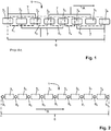
- FIG. 1 shows a sensor 1 for an impact detection and protection system according to the prior art.
- the sensor 1 comprises a plurality of sensor elements 3 1 , 3 2 ,...,3 M of a first type, arranged along an axis A of the sensor 1.
- the sensor elements 3 1 , 3 2 ,...,3 M of the first type are capacitive sensor elements.
- eight sensor elements 3 1 , 3 2 ,...,3 8 are arranged along an axis A of the sensor 1.
- the eight sensor elements 3 1 , 3 2 ,...,3 8 are connected by a wiring 7 so that the first sensor element 3 1 and the third sensor element 3 3 , the second sensor element 3 2 and the fifth sensor element 3 5 , the forth sensor element 3 4 and the seventh sensor element 3 7 , and the sixth sensor element 3 6 and the eighth sensor element 3s are connected electronically. This results in five different zones 5 1 , 5 2 ,..., 5 5 which provide five different and distinct areas of impact.
- the sensor 1 defines an effective range 6 along the axis A of the sensor 1 with a redundancy effect.
- the redundancy effect means that always two sensor elements 3 1 , 3 2 ,..., 3 8 per zone 5 1 , 5 2 ,..., 5 5 are affected at the occurrence of an impact.
- FIGS. 2 to 7 show various embodiments of a sensor 1 for an impact detection and protection system. It is to be understood that the number of the sensor elements 3 1 , 3 2 ,...,3 M of a first type and the number of the sensor elements 9 1 , 9 2 ,...,9 O of a second type mentioned in the specification below are exemplary and explanatory only and are not necessarily restrictive of the invention as claimed. Figures 2 - 7 are incorporated in and constitute a part of the specification, illustrate embodiments of the invention and together with the general description, serve to explain the principles of the invention.
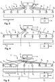
- Figure 2 shows a sensor 1 for an impact detection and protection system with two different types of sensor elements according to one embodiment of the invention.
- the sensor 1 comprises eight sensor elements 3 1 , 3 2 ,...,3 8 of a first type and nine sensor elements 9 1 , 9 2 ,...,9 9 of a second type, both of which are oriented and uniformly distributed along the axis A of the sensor 1.
- the eight sensor elements 3 1 , 3 2 ,...,3 8 of the first type and the nine sensor elements 9 1 , 9 2 ,...,9 9 of the second type are arranged such that each sensor element 3 1 , 3 2 ,...,3 8 of the first type is located between two sensor elements 9 1 , 9 2 ,...,9 9 of the second type.
- the sensor elements 3 1 , 3 2 ,..., 3 8 of the first type are capacitive sensor elements and the sensor elements 9 1 , 9 2 ,...,9 9 of the second type are piezoelectric sensor elements. Both the capacitive sensor elements and the piezoelectric sensor elements are distributed homogeneously and uniformly along the axis A of the sensor 1.
- the effective range 6 stretches from the first sensor element 9 1 of the second type to the last sensor element 9 9 of the second type.
- At least one sensor element 3 1 , 3 2 ,..., 3 8 of the first type and one neighbouring sensor element 9 1 , 9 2 ,...,9 9 of the second type must sense and be affected.
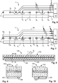
- Figure 3 shows a further embodiment of a sensor 1 for an impact detection and protection system with one sensor element 3 1 of a first type and eight sensor elements 9 1 , 9 2 ,...,9 8 of a second type.
- the sensor elements 9 1 , 9 2 ,...,9 8 of the second type are arranged along the axis A of the sensor 1.
- the sensor element 3 1 of the first type is a capacitive sensor element and electrically connected by a wiring 7 to an amplifier 13.
- the amplifier 13 amplifies a signal (change of capacity due to an impact) from the capacitive sensor element.
- the eight sensor elements 9 1 , 9 2 ,...,9 8 of the second type are piezoelectric sensor elements, which are electrically connected by a wiring 7 to an amplifier 15.
- the amplifier 13 receives eight channels 8.
- the amplifier 15 amplifies a signal (change of electric charge due to an impact) from each piezoelectric sensor element.
- the eight sensor elements 9 1 , 9 2 ,...,9 8 of the second type provide a spatial resolution with regard to the location of impact.
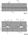
- Figure 4 shows another embodiment of a sensor 1 for an impact detection and protection system with one sensor element 3 1 of a first type and eight sensor elements 9 1 , 9 2 ,...,9 8 of a second type.
- the sensor elements 9 1 , 9 2 ,...,9 8 of the second type are arranged along the axis A of the sensor 1.
- the sensor element 3 1 of the first type is a capacitive sensor element and the eight sensor elements 9 1 , 9 2 ,...,9 8 of the second type are piezoelectric sensor elements.
- the eight sensor elements 9 1 , 9 2 ,...,9 8 of the second type are electrically connected by a wiring 7 to an amplifier 15.
- the amplifier 15 has four channels 8.
- the wiring 7 (grouping) is such that the first sensor element 9 1 and the third sensor element 9 3 are connected to the first channel 8, the second sensor element 9 2 and the fifth sensor element 9 5 are connected to the second channel 8, the fourth sensor element 9 4 and the seventh sensor element 9 7 are connected to the third channel 8 and the sixth sensor element 9 6 and eighth sensor element 9s are connected to the fourth channel 8.
- the amplifier 15 amplifies a signal (change of electric charge due to an impact) from each piezoelectric sensor element.
- the embodiment shown here has the advantage of a reduced wiring 7.
- the eight sensor elements 9 1 , 9 2 ,...,9 8 of the second type provide a location resolution (left, right or middle of the sensor 1) with regard to the location of impact.
- Figure 5 shows another embodiment of a sensor 1 for an impact detection and protection system which provides location detection of an impact by a variant of the redundancy.
- the basic construction of the sensor 1 is the same as shown in Fig. 3 and 4 .
- the difference is in the wiring 7.
- the eight sensor elements 9 1 , 9 2 ,...,9 8 of the second type are electrically connected by the wiring 7 to the amplifier 15.
- the amplifier 15 has four channels 8.
- the wiring 7 (grouping) is such that the first sensor element 9 1 and the eighth sensor element 9 8 are connected to the first channel 8, the second sensor element 9 2 and the seventh sensor element 9 7 are connected to the second channel 8, the third sensor element 9 3 and the sixth sensor element 9 6 are connected to the third channel 8 and the fourth sensor element 9 4 and the fifth sensor element 9 5 are connected to the fourth channel 8.
- the amplifier 15 amplifies a signal (change of electric charge due to an impact) from each piezoelectric sensor element.
- the embodiment shown here has the advantage of a reduced wiring 7.
- the eight sensor elements 9 1 , 9 2 ,...,9 8 of the second type provide a location resolution with regard to the location of impact. There is no possibility to discriminate between a left area 11 and a right area 12 of the sensor 1.
- Figure 6 shows an embodiment of the sensor 1 for an impact detection and protection system which is similar to the embodiment of Fig. 3 .
- the embodiment shown here differs from the embodiment of Fig. 3 in that the amplifier 13 for the capacitive sensor element 3 1 and the amplifier 15 for piezoelectric sensor elements 9 1 to 9 8 are combined in one printed circuit board 32 (see Fig. 21 and 22 ).
- the printed circuit board 32 (side mounted electronics) is provided at one end of the sensor 1. This arrangement simplifies the wiring 7 to the amplifier 13 for the capacitive sensor element 3 1 and the amplifier 15 for piezoelectric sensor elements 9 1 to 9 8 .
- the amplifier 15 for piezoelectric sensor elements has 4 channels.
- FIG. 7 shows a variant of the embodiment of the sensor 1 for an impact detection and protection system as shown in Fig. 6 .
- Each of the eight sensor elements 9 1 , 9 2 ,...,9 8 of the second type (piezoelectric sensor elements) is provided with a ground 10p.
- the ground 10 P of the first, second and third sensor element 9 1 , 9 2 , and 9 3 of the second type is connected to a first ground 10 1 .
- the ground 10 P of the fourth, fifth, sixth, seventh and eighth sensor element 9 4 , 9 5 , 9 6 , 9 7 and 9 8 of the second type is connected to a second ground 10 2 .
- the first ground 10 1 and the second ground 10 2 are connected to the amplifier 15 for piezoelectric sensor elements.
- Figure 8 shows a schematic view of a carrier 100 for the sensor 1.
- the sensor 1 is sandwiched between a first foam element 102 and a second foam element 104.
- the first foam element 102 and the second foam element 104 are arranged such that the sensor 1 is completely enclosed within the first foam element 102 and the second foam element.
- At least the second foam element 104 has a flat outline for mechanical integration.
- the carrier 100 is mounted with the second foam element 104 to a structural element 105 of a vehicle (not shown).
- the first foam element 102 faces into a driving direction D of the vehicle.
- Figure 9 and 10 show various embodiments of the carrier 100 for the sensor 1 taken along the section B-B of Figure 8 .
- the sensor 1 is completely enclosed by the first foam element 102 and the second foam element 104.
- the first foam element 102 of the carrier 100 shown in Fig. 9 has a flat surface, pointing in the driving direction D (see Fig. 8 ).
- the first foam element 102 of the carrier 100 shown in Fig. 10 has a curved surface, pointing in the driving direction D (see Fig. 8 ). It is to be understood that the design of the surface, pointing in the driving direction D, is not limited to the structures shown in Fig. 9 and 10 .
- the variation of the design of carrier 100 depends on the size and the height of the sensor 1 to be enclosed.
- Figure 11 shows a partial view of the sensor 1 layered between a first foam element 102 and a second foam element 104 of the carrier 100.
- the sensor 1 comprises at least one the sensor element 3 1 , 3 2 ,...,3 M of a first type (here not shown) and a plurality of sensor elements 9 1 , 9 2 ,...,9 O of a second type (here not shown).
- the sensor 1 is sandwiched between the first foam element 102 and the second foam element 104.
- Figure 12 shows a partial cross-sectional view of an embodiment of the formation of the carrier, which houses the piezoelectric sensor elements and the capacitive sensor element.
- the first foam element 102 has a plurality of dome shaped cavities 110, wherein the sensor elements 9 1 , 9 2 ,...,9 O of the second type (piezoelectric sensor elements) are placed in the apex 112 of each dome shaped cavity 110.
- the wiring 7 for the sensor elements 9 1 , 9 2 ,...,9 O of the second type are as well arranged between the first foam element 102 and the second foam element 104.
- a single sensor element 3 1 of the first type (capacitive sensor element) is placed as well between the first foam element 102 and the second foam element 104.
- Figure 13 shows an enlarged view of the placement of a piezoelectric sensor element (sensor elements 9 1 , 9 2 ,..., 9 O of the second type) within the carrier 100.
- the sensor element 9 2 , of the second type is placed in the apex 112 of the not deformed dome shaped cavity 110.
- the deformed state due to a collision, is shown in Figure 14 .
- a collision of the vehicle causes the not deformed dome shaped cavity 110 to be transferred to a deformed dome shaped cavity 111.
- the deformed dome shaped cavity 111 causes a deformation of the piezoelectric sensor element (sensor element 9 2 of the second type) within the deformed dome shaped cavity 111.
- the deformation causes a voltage signal in the piezoelectric sensor element which is sensed by the amplifier 15 (see Figures 3-7 ) for the piezoelectric sensor element.
- Figure 15 shows a schematic, partial view of the arrangement of the sensor elements 3 3 and 3 4 of the first type (capacitive sensor elements; electrodes) and of the sensor element 9 4 of the second type (piezoelectric sensor element).
- the piezoelectric sensor element is placed in the apex 112 of the dome shaped cavity 110.
- Another embodiment of the arrangement of the sensor elements 3 3 and 3 4 of the first type (capacitive sensor elements, electrodes) and of the sensor elements 9 4 of the second type (piezoelectric sensor element) is shown in Figure 16 .
- the piezoelectric sensor element is placed in the apex 112 of the dome shaped cavity 110.
- the sensor elements 3 3 and 3 4 of the first type (capacitive sensor elements, electrodes) are covered by a sealing layer 17.
- Figure 17 shows an embodiment of the arrangement of at least one sensor element 3 1 of the first type (capacitive sensor element) inside the carrier 100.
- the sensor element 3 1 of the first type is arranged in an undulating manner between the first foam element 102 and the second foam element 104.
- An object 50 deforming at least the first foam element 102 in the impact direction DI causes a mechanical strain on the at least one sensor element 3 1 of the first type.
- Figure 18 shows the effect of a collision on the sensor element 3 1 of the first type (capacitive sensor element) in the carrier 100 (see for example Fig 8 ).
- the sensor element 3 1 of the first type is provided in a not undulating manner.
- An impact of an object 50 (see Fig. 17 ) causes a strained sensor element 3D 1 of the first type.
- the strain might cause a rupture of the strained sensor element 3D 1 of the first type, which results in a malfunction of the sensor 1.
- the effect of a collision on an undulated sensor element 3 1 of the first type (capacitive sensor element) according to the arrangement shown in the embodiment of Fig. 17 is shown in Figure 19 .
- a collision here causes less strain on the sensor element 3 1 of the first type than in the example of Fig. 18 .
- Figure 20 shows a schematic side view and Figure 21 shows a schematic top view of the integration of the sensor 1 in a sensor device 30 which is ready to use in a vehicle (not shown).
- the sensor 1 is enclosed in a sealing 31, which seals the sensor and the associated electronics (for example, sensor 1) against the influence of humidity and/or dirt and provides an electromagnetic shielding for the electronics.
- the sensor 1 is connected by the required wiring 7 to a printed circuit board 31.
- the printed circuit board 31 encompasses the amplifier 13 for capacitive sensor elements (not shown here) and the amplifier 15 for piezoelectric sensor elements (not shown here). More precisely, the amplifiers 13 and 15 are realised by an ASIC 33 on the printed circuit board 31.
- the printed circuit board 31 is enclosed in a housing 34, which is closed at one end by a connector 37 and on the opposite end by the sensor 1.
- a pressure equalizing system 35 is provided in order to keep the pressure inside the housing 34 approximately at a constant level.
- the connector 37 has connector pins 38 which provide an electrical connection to a control system (not shown) of the vehicle.
- the carrier 100 with the enclosed sensor 1 is surrounded by a sealing 31. At one end the sealing is closed by a welded end 36 and at an opposite end the sealing (31) is attached to an inner wall 41 of the housing 34.
- Figure 22 is an enlarged view of the area marked with a dashed circle 39 in Fig. 20 .
- the sensor 1 is fixed to the housing 34.
- the sealing 31 is attached by one side to the sensor 1 and by the opposite side to the housing 34.
- the attachment of the sealing 31 to the housing 34 is achieved with a glue 40.
- the sealing 31 is attached to an inner wall 41 of the housing 34.
- Figure 23 shows a schematic view of the arrangement of the components of the sensor device 30.
- the at least one sensor element 3 1 , 3 2 ,...,3 M of a first type (capacitive sensor element) and the sensor elements 9 1 , 9 2 ,...,9 O of a second type (piezoelectric sensor elements) of the inventive sensor 1 are connected with a wiring 7 to the amplifier 13 for capacitive sensor elements and the amplifier 15 for piezoelectric sensor elements.
- the at least one sensor element 3 1 , 3 2 ,...,3 M of a first type and the sensor elements 9 1 , 9 2 ,...,9 O of a second type are connected to a common ground 10.
- the amplifier 13 for capacitive sensor elements and the amplifier 15 for piezoelectric sensor elements is realized on one chip, for example the ASIC 33. Both amplifiers 13 and 15 are connected to a digital interface 42 which is a digital, two-wire interface 42 for sensors in vehicle electronics.
- Figure 24 shows a schematic view of the placement of the printed circuit board 32 (electronics) in relation to the sensor 1.
- the printed circuit board 32 is placed in the middle of the sensor 1 so that the sensor 1 has a left sensor 1L and a right sensor 1R.
- Figure 25 shows an alternative embodiment of the inventive sensor 1.
- the inventive sensor 1 comprises one sensor element 3 1 of a first type and a plurality sensor elements 9 1 , 9 2 ,...,9 O of a second type which are accelerometers.
- the accelerometers of the sensor 1 are placed close to the bumper (not shown) of the vehicle.
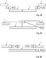
- Figure 26 shows a schematic view of a further embodiment of the placement of the printed circuit boards 32 (electronics) in relation to the inventive sensors 1.
- Four individual sensors 1 are arranged symmetrically, wherein two of the four sensors 1 are connected to one printed circuit board 32.
- Each of the two printed circuit boards 32 is connected to a respective digital interface 42.
- Figure 27 shows a schematic view of an additional embodiment of the placement of the printed circuit board 32 (electronics) in relation to the inventive sensors 1.
- Three individual sensors 1 are arranged such that the three sensors 1 are connected to a single common printed circuit board 32.
- the printed circuit board 32 is connected to a digital interface 42.
- Figure 28 shows a schematic view of an additional embodiment of the placement of printed circuit boards 32 (electronics) in relation to three individual inventive sensors 1.
- Each individual sensor 1 is connected to a respective printed circuit board 32.
- Each of the three printed circuit boards 32 is connected to a digital interface 42.
Landscapes
- Physics & Mathematics (AREA)
- General Physics & Mathematics (AREA)
- Force Measurement Appropriate To Specific Purposes (AREA)
Abstract
Description
- The invention relates to a sensor for an impact detection and protection system, wherein the sensor defines an axis.
- The invention relates as well to an impact detection and protection system for a vehicle.
- The European Patent
EP 2 709 877 B1 relates to a motor vehicle comprising a fender provided at the front and the rear and at least one sensor device, which has a capacitively operating sensor. The sensor device has an associated control device for collision detection, wherein the sensor is arranged on a fender. The sensor is formed as a surface sensor which extends over at least half the width of the fender. The control device is able to determine information resulting from a collision with an object by using the capacitance of the sensor, which changes as a result of collision-induced deformation of the sensor. - US Patent
US 9,650,013 B1 - It is therefore an object of the present invention to provide a sensor for an impact detection and protection which has redundancy, provides an impact recognition, enables a diagnosis and allows a simplified integration in a vehicle.
- The above object is achieved by a sensor for an impact detection and protection system for a vehicle which comprises the features of
claim 1. -
Claim 7 is directed to an impact detection and protection system including such a sensor. - According to an inventive embodiment a sensor for an impact detection and protection system defines an axis. Especially the sensor is used to provide some protection for a pedestrian in case an impact happens. The axis is essentially parallel to or aligned with a front face of a vehicle. The sensor has at least one sensor element of a first type, which is oriented along the axis of the sensor. Additionally, the sensor has a plurality of sensor elements of a second type, which are oriented and uniformly distributed along the axis of the sensor. The advantage of the two different sensor types is a redundancy, wherein both sensor types are integrated in one sensor. Furthermore, the sensor allows the determination of location of the impact at the front side of the vehicle. The impact location can be achieved by the at least one sensor element of the first type and/or the plurality of sensor elements of the second type.
- According to one embodiment of the invention the at least one sensor element of the first type is a capacitive sensor and the plurality of sensor elements of the second type are piezoelectric sensor elements. According to a further embodiment of the invention the at least one sensor element of the first type is a capacitive sensor and the plurality of sensor elements of the second type are accelerometers. According to a still further embodiment of the invention the at least one sensor element of the first type is a capacitive sensor and the plurality of sensor elements of the second type are force sensitive sensor elements. Moreover the plurality of sensor elements of the second type can be as well a mixture above mentioned sensor elements of the second type.
- According to one possible embodiment of the invention the sensor comprises one single sensor element of the first type and the plurality of sensor elements of the second type. The plurality of sensor elements of the second type are oriented and are separated equally along the axis of the sensor. According to a further embodiment the plurality of sensor elements of the second type can separated unequally along the axis of the sensor. The axis of the sensor is essentially parallel to the orientation of the sensor element of the first type.
- For the collection of signals from the at least one sensor element of the first type, the at least one sensor element is electrically connected by a wiring to a first amplifier. According to a preferred embodiment the sensor comprises one single capacitive sensor, which is connected to the first amplifier. The operating mode of the at least one capacitive sensor is that an impact causes a distance change of the two electrodes of the capacitive sensor. The change in distance of the electrodes results in a capacitive change, which is amplified and used for the verification of the impact.
- According to one possible embodiment of the invention each of the plurality of sensor elements of the second type is electrically connected by a wiring to a second amplifier. According to a preferred embodiment the sensor comprises for example eight sensor elements of the second type (piezoelectric sensor elements). The eight piezoelectric sensor elements are connected to eight channels of the second amplifier by an individual wiring.
- According to another possible embodiment of the invention two of the plurality of sensor elements of the second type are commonly connected by a wiring to the second amplifier. Consequently, the second amplifier has four channels to which the eight piezoelectric sensor elements are connected in pairs.
- According to one embodiment, the pairing of the eight piezoelectric sensor elements is such that the first and the third piezoelectric sensor elements are connected to the first channel, the second and the fifth piezoelectric sensor elements are connected to the second channel, the fourth and the seventh piezoelectric sensor elements are connected to the third channel and the sixth and the eighth piezoelectric sensor elements are connected to the forth channel. The advantage of this embodiment is the minimum wiring for the capacitive sensor element and a location resolution between the left, the right and the middle of the sensor.
- According to a further embodiment, the pairing of the eight piezoelectric sensor elements is such that the first and the eighth piezo electric sensor elements are connected to the first channel, the second and the seventh piezoelectric sensor elements are connected to the second channel, the third and the sixth piezoelectric sensor elements are connected to the third channel and the fourth and the fifth piezoelectric sensor elements are connected to the fourth channel. The advantage of this embodiment is the minimum wiring for the capacitive sensor element and symmetric areas on the left and the right of the sensor.
- According to a further embodiment the amplifier for the one capacitive sensor element and the amplifier for the eight piezoelectric sensor elements are combined in one printed circuit board. The printed circuit board is provided at one end of the sensor. The advantage of this arrangement is a simplification of the wiring to the amplifier for the capacitive sensor element and the amplifier for piezoelectric sensor elements. As mentioned above the arrangement of the piezoelectric sensor elements provides a location resolution of the location of impact. According to a further embodiment, all the piezoelectric sensor elements of the sensor can be connected to ground potential.
- In order to use the inventive sensor in the field, a carrier for the sensor is provided. According to one potential embodiment, the sensor is enclosed within the carrier. The carrier is deformable by an impacting object (for example a pedestrian). The impact causes a deformation and an electrical signal from the at least one sensor element of the first type and the plurality of sensor elements of the second type.
- According to one embodiment of the invention the carrier has a first foam element and a second foam element. The first foam element and the second foam element enclose the sensor and are in mechanical contact with the sensor. At least the first foam element, being essentially perpendicular to the direction of driving, is deformable by the impact of the object. The impact causes a deformation and an electrical signal from the at least one sensor element of the first type and the plurality of sensor elements of the second type. The sensor elements of the second type provide information about the location of the impact.
- According to one preferred embodiment of the invention a plurality of dome shaped cavities are formed in the first foam element. Each of the dome shaped cavities defines an apex and is open to the second foam element. One single sensor element, which is a piezoelectric sensor element, of the plurality of sensor elements of the second type is attached to the apex. The at least one sensor element of the first type of the sensor is supported by the second foam element of the carrier. In the embodiment as discussed here the domes are oriented towards the direction of impact. According to another embodiment, the domes can be oriented with the apex pointing toward a structural element (cross member) of the vehicle.
- According to one possible embodiment of the invention the sensor, configured for use and mounting in a vehicle, comprises the carrier with the enclosed sensor, which is surrounded by a sealing. The sealing has at one end a welded end and at an opposite end the sealing is attached to an inner wall of a housing (end cap). According to a preferred embodiment the sealing can be attached to the inner wall of the housing with a glue. The housing is closed at one end by the sealing, which is attached to the inner wall of the housing, and at the other end by a connector.
- A printed circuit board is placed inside the housing. The first amplifier and the second amplifier are realized on the printed circuit board. The at least one sensor element of the first type is connected by a wiring to the first amplifier and the plurality of sensor elements of the second type are connected by a wiring to the second amplifier.
- According to a preferred embodiment the second amplifier has four channels and the wiring for the plurality of sensor elements of the second type is such that the plurality of sensor elements of the second type are grouped and connected to the four channels. The first amplifier and the second amplifier are connected to a digital interface, which is a digital, two-wire interface for sensors in vehicle electronics. According to a preferred embodiment, the first amplifier, the second amplifier and the digital interface are realized by an ASIC.
- It is to be understood that both the foregoing general description and the following detailed description are exemplary and explanatory only and are not necessarily restrictive of the present disclosure. The accompanying drawings, which are incorporated in and constitute a part of the specification, illustrate subject matter of the disclosure. Together, the descriptions and the drawings serve to explain the principles of the disclosure. The mentioned numbers of the sensor elements of the first type and the sensor elements of the second type are utilised to explain the invention and should not be regarded as a limiting factor of the invention.
- The numerous advantages of the disclosure may be better understood by those skilled in the art by reference to the accompanying figures in which:
-
FIG. 1 shows a prior art sensor for an impact protection system. -
FIG. 2 shows an inventive sensor for an impact protection system with two different types of sensor elements according to one embodiment of the invention. -
FIG. 3 shows a sensor for an impact protection system with two different types of sensor elements according to a further embodiment of the invention. -
FIG. 4 shows a sensor for an impact protection system with two different types of sensor elements according the embodiment ofFig. 3 but with a different wiring. -
FIG. 5 shows a sensor for an impact protection system with two different types of sensor elements according the embodiment ofFig. 3 but with another embodiment of the wiring. -
FIG. 6 shows a sensor for an impact protection system with two different types of sensor elements according the embodiment ofFig. 3 but with a further embodiment of the wiring. -
FIG. 7 shows a sensor for an impact protection system with two different types of sensor elements according the embodiment ofFig. 3 but with a further embodiment of the wiring. -
FIG. 8 shows a schematic view of a carrier for the embedded sensor. -
FIG. 9 shows a cross section of the carrier along line B-B ofFig 8 . -
FIG. 10 shows a cross section of another embodiment of the carrier along line B-B ofFig 8 . -
FIG. 11 shows a partial view of the sensor layered between a first and a second element of the carrier. -
FIG. 12 shows an embodiment of the formation of the carrier which houses the piezoelectric sensor elements and the capacitive sensor element. -
FIG. 13 shows an enlarged view of the placement of a piezoelectric sensor element within the carrier. -
FIG. 14 shows an enlarged view of the deformation of the dome shaped cavity due to an occurred collision which causes a sensing signal by the piezoelectric sensor element. -
FIG. 15 shows a schematic, partial view of the arrangement of the capacitive sensor elements and the piezoelectric sensor elements. -
FIG. 16 shows a schematic, partial view of another embodiment of the arrangement of the capacitive sensor elements and the piezoelectric sensor elements. -
FIG. 17 shows an embodiment of the arrangement of at least one sensor element of the first type (capacitive sensor element) in the carrier. -
FIG. 18 shows the effect of a collision on the capacitive sensor element in the carrier. -
FIG. 19 shows the effect of a collision on the capacitive sensor element according to the arrangement shown in the embodiment ofFig. 17 . -
FIG. 20 shows a schematic side view of the integration of the sensor in a sensor device. -
FIG. 21 shows a schematic top view of the integration of the sensor in the sensor device of -
Fig. 20 . -
FIG. 22 shows a detailed view of the mounting the sensor to the housing. -
FIG. 23 shows a schematic view of the arrangement of the components of the system according to one embodiment. -
FIG. 24 shows a schematic view of the placement of the electronics in relation to the sensor. -
FIG. 25 shows an alternative embodiment of the inventive sensor. -
FIG. 26 shows a schematic view of a further embodiment of the placement of the electronics in relation to the inventive sensors. -
FIG. 27 shows a schematic view of an additional embodiment of the placement of the electronics in relation to the inventive sensors. -
FIG. 28 shows a schematic view of an additional embodiment of the placement of the electronics in relation to the inventive sensors. - Same reference numerals refer to same elements or elements of similar function throughout the various figures. Furthermore, only reference numerals necessary for the description of the respective figure are shown in the figures. The shown embodiments represent only examples of how the invention can be carried out. This should not be regarded as a limitation of the invention.
-
FIG. 1 shows asensor 1 for an impact detection and protection system according to the prior art. Thesensor 1 comprises a plurality ofsensor elements sensor 1. Thesensor elements sensor elements sensor 1. The eightsensor elements wiring 7 so that thefirst sensor element 31 and thethird sensor element 33, thesecond sensor element 32 and thefifth sensor element 35, theforth sensor element 34 and theseventh sensor element 37, and thesixth sensor element 36 and the eighth sensor element 3s are connected electronically. This results in five different zones 51, 52,..., 55 which provide five different and distinct areas of impact. With thewiring 7 mentioned above thesensor 1 defines aneffective range 6 along the axis A of thesensor 1 with a redundancy effect. The redundancy effect means that always twosensor elements - The
Figures 2 to 7 show various embodiments of asensor 1 for an impact detection and protection system. It is to be understood that the number of thesensor elements sensor elements Figures 2 - 7 are incorporated in and constitute a part of the specification, illustrate embodiments of the invention and together with the general description, serve to explain the principles of the invention. -
Figure 2 shows asensor 1 for an impact detection and protection system with two different types of sensor elements according to one embodiment of the invention. According the embodiment shown here, thesensor 1 comprises eightsensor elements sensor elements sensor 1. The eightsensor elements sensor elements sensor element sensor elements sensor elements sensor elements sensor 1. Theeffective range 6 stretches from thefirst sensor element 91 of the second type to thelast sensor element 99 of the second type. For sensing an impact at least onesensor element sensor element -
Figure 3 shows a further embodiment of asensor 1 for an impact detection and protection system with onesensor element 31 of a first type and eightsensor elements sensor elements sensor 1. Thesensor element 31 of the first type is a capacitive sensor element and electrically connected by awiring 7 to anamplifier 13. Theamplifier 13 amplifies a signal (change of capacity due to an impact) from the capacitive sensor element. The eightsensor elements wiring 7 to anamplifier 15. Consequently, theamplifier 13 receives eightchannels 8. Theamplifier 15 amplifies a signal (change of electric charge due to an impact) from each piezoelectric sensor element. In case of an impact the eightsensor elements -
Figure 4 shows another embodiment of asensor 1 for an impact detection and protection system with onesensor element 31 of a first type and eightsensor elements sensor elements sensor 1. Thesensor element 31 of the first type is a capacitive sensor element and the eightsensor elements sensor elements wiring 7 to anamplifier 15. Theamplifier 15 has fourchannels 8. The wiring 7 (grouping) is such that thefirst sensor element 91 and thethird sensor element 93 are connected to thefirst channel 8, thesecond sensor element 92 and thefifth sensor element 95 are connected to thesecond channel 8, thefourth sensor element 94 and theseventh sensor element 97 are connected to thethird channel 8 and thesixth sensor element 96 and eighth sensor element 9s are connected to thefourth channel 8. Theamplifier 15 amplifies a signal (change of electric charge due to an impact) from each piezoelectric sensor element. The embodiment shown here has the advantage of a reducedwiring 7. In case of an impact the eightsensor elements -
Figure 5 shows another embodiment of asensor 1 for an impact detection and protection system which provides location detection of an impact by a variant of the redundancy. The basic construction of thesensor 1 is the same as shown inFig. 3 and 4 . The difference is in thewiring 7. The eightsensor elements wiring 7 to theamplifier 15. Theamplifier 15 has fourchannels 8. The wiring 7 (grouping) is such that thefirst sensor element 91 and theeighth sensor element 98 are connected to thefirst channel 8, thesecond sensor element 92 and theseventh sensor element 97 are connected to thesecond channel 8, thethird sensor element 93 and thesixth sensor element 96 are connected to thethird channel 8 and thefourth sensor element 94 and thefifth sensor element 95 are connected to thefourth channel 8. Theamplifier 15 amplifies a signal (change of electric charge due to an impact) from each piezoelectric sensor element. The embodiment shown here has the advantage of a reducedwiring 7. In case of an impact the eightsensor elements left area 11 and aright area 12 of thesensor 1. -
Figure 6 shows an embodiment of thesensor 1 for an impact detection and protection system which is similar to the embodiment ofFig. 3 . The embodiment shown here differs from the embodiment ofFig. 3 in that theamplifier 13 for thecapacitive sensor element 31 and theamplifier 15 forpiezoelectric sensor elements 91 to 98 are combined in one printed circuit board 32 (seeFig. 21 and22 ). The printed circuit board 32 (side mounted electronics) is provided at one end of thesensor 1. This arrangement simplifies thewiring 7 to theamplifier 13 for thecapacitive sensor element 31 and theamplifier 15 forpiezoelectric sensor elements 91 to 98. As known from the embodiment ofFig. 3 theamplifier 15 for piezoelectric sensor elements has 4 channels. -
Figure 7 shows a variant of the embodiment of thesensor 1 for an impact detection and protection system as shown inFig. 6 . Each of the eightsensor elements ground 10p. Theground 10P of the first, second andthird sensor element first ground 101. Theground 10P of the fourth, fifth, sixth, seventh andeighth sensor element second ground 102. Thefirst ground 101 and thesecond ground 102 are connected to theamplifier 15 for piezoelectric sensor elements. -
Figure 8 shows a schematic view of acarrier 100 for thesensor 1. Thesensor 1 is sandwiched between afirst foam element 102 and asecond foam element 104. Thefirst foam element 102 and thesecond foam element 104 are arranged such that thesensor 1 is completely enclosed within thefirst foam element 102 and the second foam element. At least thesecond foam element 104 has a flat outline for mechanical integration. For example, thecarrier 100 is mounted with thesecond foam element 104 to astructural element 105 of a vehicle (not shown). Thefirst foam element 102 faces into a driving direction D of the vehicle. -
Figure 9 and 10 show various embodiments of thecarrier 100 for thesensor 1 taken along the section B-B ofFigure 8 . Thesensor 1 is completely enclosed by thefirst foam element 102 and thesecond foam element 104. Thefirst foam element 102 of thecarrier 100 shown inFig. 9 has a flat surface, pointing in the driving direction D (seeFig. 8 ). Thefirst foam element 102 of thecarrier 100 shown inFig. 10 has a curved surface, pointing in the driving direction D (seeFig. 8 ). It is to be understood that the design of the surface, pointing in the driving direction D, is not limited to the structures shown inFig. 9 and 10 . The variation of the design ofcarrier 100 depends on the size and the height of thesensor 1 to be enclosed. -
Figure 11 shows a partial view of thesensor 1 layered between afirst foam element 102 and asecond foam element 104 of thecarrier 100. As mentioned above, thesensor 1 comprises at least one thesensor element sensor elements sensor 1 is sandwiched between thefirst foam element 102 and thesecond foam element 104. -
Figure 12 shows a partial cross-sectional view of an embodiment of the formation of the carrier, which houses the piezoelectric sensor elements and the capacitive sensor element. Thefirst foam element 102 has a plurality of dome shapedcavities 110, wherein thesensor elements cavity 110. Thewiring 7 for thesensor elements first foam element 102 and thesecond foam element 104. Asingle sensor element 31 of the first type (capacitive sensor element) is placed as well between thefirst foam element 102 and thesecond foam element 104. -
Figure 13 shows an enlarged view of the placement of a piezoelectric sensor element (sensor elements carrier 100. Thesensor element 92, of the second type is placed in the apex 112 of the not deformed dome shapedcavity 110. The deformed state, due to a collision, is shown inFigure 14 . A collision of the vehicle (not shown) causes the not deformed dome shapedcavity 110 to be transferred to a deformed dome shapedcavity 111. The deformed dome shapedcavity 111 causes a deformation of the piezoelectric sensor element (sensor element 92 of the second type) within the deformed dome shapedcavity 111. The deformation causes a voltage signal in the piezoelectric sensor element which is sensed by the amplifier 15 (seeFigures 3-7 ) for the piezoelectric sensor element. -
Figure 15 shows a schematic, partial view of the arrangement of thesensor elements sensor element 94 of the second type (piezoelectric sensor element). The piezoelectric sensor element is placed in the apex 112 of the dome shapedcavity 110. Another embodiment of the arrangement of thesensor elements sensor elements 94 of the second type (piezoelectric sensor element) is shown inFigure 16 . Here the piezoelectric sensor element is placed in the apex 112 of the dome shapedcavity 110. Thesensor elements sealing layer 17. -
Figure 17 shows an embodiment of the arrangement of at least onesensor element 31 of the first type (capacitive sensor element) inside thecarrier 100. Thesensor element 31 of the first type is arranged in an undulating manner between thefirst foam element 102 and thesecond foam element 104. Anobject 50 deforming at least thefirst foam element 102 in the impact direction DI causes a mechanical strain on the at least onesensor element 31 of the first type. -
Figure 18 shows the effect of a collision on thesensor element 31 of the first type (capacitive sensor element) in the carrier 100 (see for exampleFig 8 ). Thesensor element 31 of the first type is provided in a not undulating manner. An impact of an object 50 (seeFig. 17 ) causes a strained sensor element 3D1 of the first type. The strain might cause a rupture of the strained sensor element 3D1 of the first type, which results in a malfunction of thesensor 1. The effect of a collision on an undulatedsensor element 31 of the first type (capacitive sensor element) according to the arrangement shown in the embodiment ofFig. 17 is shown inFigure 19 . A collision here causes less strain on thesensor element 31 of the first type than in the example ofFig. 18 . -
Figure 20 shows a schematic side view andFigure 21 shows a schematic top view of the integration of thesensor 1 in asensor device 30 which is ready to use in a vehicle (not shown). Thesensor 1 is enclosed in a sealing 31, which seals the sensor and the associated electronics (for example, sensor 1) against the influence of humidity and/or dirt and provides an electromagnetic shielding for the electronics. Thesensor 1 is connected by the requiredwiring 7 to a printedcircuit board 31. The printedcircuit board 31 encompasses theamplifier 13 for capacitive sensor elements (not shown here) and theamplifier 15 for piezoelectric sensor elements (not shown here). More precisely, theamplifiers ASIC 33 on the printedcircuit board 31. The printedcircuit board 31 is enclosed in ahousing 34, which is closed at one end by aconnector 37 and on the opposite end by thesensor 1. Apressure equalizing system 35 is provided in order to keep the pressure inside thehousing 34 approximately at a constant level. Theconnector 37 has connector pins 38 which provide an electrical connection to a control system (not shown) of the vehicle. Thecarrier 100 with theenclosed sensor 1 is surrounded by a sealing 31. At one end the sealing is closed by a weldedend 36 and at an opposite end the sealing (31) is attached to aninner wall 41 of thehousing 34. -
Figure 22 is an enlarged view of the area marked with a dashedcircle 39 inFig. 20 . Thesensor 1 is fixed to thehousing 34. The sealing 31 is attached by one side to thesensor 1 and by the opposite side to thehousing 34. The attachment of the sealing 31 to thehousing 34 is achieved with aglue 40. In the embodiment shown here the sealing 31 is attached to aninner wall 41 of thehousing 34. -
Figure 23 shows a schematic view of the arrangement of the components of thesensor device 30. The at least onesensor element sensor elements inventive sensor 1 are connected with awiring 7 to theamplifier 13 for capacitive sensor elements and theamplifier 15 for piezoelectric sensor elements. Additionally, the at least onesensor element sensor elements common ground 10. Theamplifier 13 for capacitive sensor elements and theamplifier 15 for piezoelectric sensor elements is realized on one chip, for example theASIC 33. Bothamplifiers digital interface 42 which is a digital, two-wire interface 42 for sensors in vehicle electronics. -
Figure 24 shows a schematic view of the placement of the printed circuit board 32 (electronics) in relation to thesensor 1. The printedcircuit board 32 is placed in the middle of thesensor 1 so that thesensor 1 has aleft sensor 1L and aright sensor 1R. -
Figure 25 shows an alternative embodiment of theinventive sensor 1. Theinventive sensor 1 comprises onesensor element 31 of a first type and aplurality sensor elements sensor 1 are placed close to the bumper (not shown) of the vehicle. -
Figure 26 shows a schematic view of a further embodiment of the placement of the printed circuit boards 32 (electronics) in relation to theinventive sensors 1. Fourindividual sensors 1 are arranged symmetrically, wherein two of the foursensors 1 are connected to one printedcircuit board 32. Each of the two printedcircuit boards 32 is connected to a respectivedigital interface 42. -
Figure 27 shows a schematic view of an additional embodiment of the placement of the printed circuit board 32 (electronics) in relation to theinventive sensors 1. Threeindividual sensors 1 are arranged such that the threesensors 1 are connected to a single common printedcircuit board 32. The printedcircuit board 32 is connected to adigital interface 42. -
Figure 28 shows a schematic view of an additional embodiment of the placement of printed circuit boards 32 (electronics) in relation to three individualinventive sensors 1. Eachindividual sensor 1 is connected to a respective printedcircuit board 32. Each of the three printedcircuit boards 32 is connected to adigital interface 42. - It is believed that the present disclosure and many of its attendant advantages will be understood by the foregoing description, and it will be apparent that various changes may be made in the form, construction and arrangement of the components without departing from the disclosed subject matter or without sacrificing all of its material advantages. The form described is merely explanatory, and it is the intention of the following claims to encompass and include such changes. Accordingly, the scope of the invention should be limited only by the claims appended hereto.
-
- 1
- Sensor
- 1L
- left sensor
- 1R
- right sensor
- 31, 32,...,3M
- sensor element of a first type
- 51, 52,...,5N
- zone
- 6
- effective range
- 7
- wiring
- 8
- channel
- 91, 92,...,9O
- sensor element of a second type
- 10
- common ground
- 101
- first ground
- 102
- second ground
- 10P
- ground piezoelectric elements
- 11
- left area
- 12
- right area
- 13
- first amplifier
- 15
- second amplifier
- 17
- sealing layer
- 30
- sensor device
- 31
- sealing
- 32
- printed circuit board
- 33
- ASIC
- 34
- housing
- 35
- pressure equalizing system
- 36
- welded end
- 37
- connector
- 38
- connector pin
- 39
- circle
- 40
- glue
- 41
- inner wall
- 42
- digital interface
- 50
- object
- 100
- carrier
- 102
- first foam element
- 104
- second foam element
- 105
- structural element
- 110
- dome shaped cavity
- 111
- deformed dome shaped cavity
- 112
- apex
- A
- axis
- B-B
- section
- D
- driving direction
- DI
- impact direction
Claims (15)
- A sensor (1) for an impact detection and protection system defining an axis (A):
characterized by• at least one sensor element (31, 32,...,3M) of a first type, oriented along the axis (A) of the sensor (1); and• a plurality of sensor elements (91, 92,...,9O) of a second type, oriented and uniformly distributed along the axis (A) of the sensor (1). - The sensor (1) as claimed in claim 1, wherein the at least one sensor element (31, 32,..., 3M) of the first type is a capacitive sensor and the plurality of sensor elements (91, 92,...,9O) of the second type are piezoelectric sensor elements, force sensitive sensor elements or accelerometers.
- The sensor (1) as claimed in any preceding claim, wherein the sensor (1) comprises one sensor element (31) of the first type and the plurality of sensor elements (91, 92,...,9O) of the second type, wherein the plurality of sensor elements (91, 92,...,9O) of the second type are oriented and are separated equally or unequally along the axis (A) of the sensor (1).
- The sensor (1) as claimed in any preceding claim, wherein at least one sensor element (31, 32,...,3M) of the first type is electrically connected by a wiring (7) to a first amplifier (13).
- The sensor (1) as claimed in any preceding claim 1 - 4, wherein each of the plurality of sensor elements (91, 92,...,9O) of the second type is electrically connected by a wiring (7) to a second amplifier (15).
- The sensor (1) as claimed in any preceding claim 1 - 4, wherein two of the plurality of sensor elements (91, 92,...,9O) of the second type are commonly connected by a wiring (7) to a second amplifier (15).
- An impact detection and protection system for a vehicle utilizing a sensor (1) as claimed in any one of the preceding claims 1 - 6, characterized by:- a carrier (100), wherein the sensor (1) is enclosed within the carrier (100), wherein the carrier (100) is deformable by an impacting object (50) and configured, upon a deformation, to thereby cause a deformation of and an electrical signal from the at least one sensor element (31, 32,...,3M) of the first type and the plurality of sensor elements (91, 92,...,9O) of the second type.
- The impact detection and protection system (30) as claimed in claim 7, wherein the carrier (100) is defined by an arrangement of a first foam element (102) and a second foam element (104), both of which enclose the sensor (1) and are in mechanical contact with the sensor (1), wherein at least the first foam element (102) is deformable by an impacting object (50) and configured, upon a deformation, to thereby cause a deformation and an electrical signal from the at least one sensor element (31, 32,...,3M) of the first type and the plurality of sensor elements (91, 92,...,9O) of the second type.
- The impact detection and protection system (30) as claimed in claims 7 to 8, wherein a plurality of dome shaped cavities (110) are formed in the first foam element (102) so that each of the dome shaped cavities (110) defines an apex (112) and is open to the second foam element (104), and one single sensor element (91, 92,...,9O) which is a piezoelectric sensor element of the plurality of sensor elements (91, 92,...,9O) of the second type is attached to the apex (112).
- The impact detection and protection system (30) as claimed in any of the preceding claims 7 - 9, wherein the at least one sensor element (31, 32,..., 3M) of the first type of the sensor (1) is supported by the second foam element (104) of the carrier (100).
- The impact detection and protection system (30) as claimed in any of the claims 7 to 10, wherein the carrier (100) with the enclosed sensor (1) is surrounded by a sealing (31) which has at one end a welded end (36) and at an opposite end the sealing (31) is attached to an inner wall (41) of a housing (34).
- The impact detection and protection system (30) as claimed in claim 11, wherein the sealing (31) is attached to the inner wall (41) of the housing (34) with a glue (40).
- The impact detection and protection system (30) as claimed in any of the claims 11 to 12, wherein the housing (34) is closed at one end by the sealing (31) which is attached to the inner wall of the housing (34) and at the other end by a connector (37).
- The impact detection and protection system (30) as claimed in any of the claims 11 to 13, wherein a printed circuit board (31) with the first amplifier (13) an the second amplifier (15) is positioned inside the housing (34), wherein the at least one sensor element (31, 32,...,3M) of the first type is connected by a wiring (7) to the first amplifier (13), and the plurality of sensor elements (91, 92,...,9O) of the second type are connected by the wiring (7) to the second amplifier (15).
- The impact detection and protection system (30) as claimed in claim 14, wherein the second amplifier (15) has four channels (8) and the wiring (7) for the plurality of sensor elements (91, 92,...,9O) of the second type is such that the plurality of sensor elements (91, 92,...,9O) of the second type are grouped and connected to the four channels (8).
Priority Applications (3)
| Application Number | Priority Date | Filing Date | Title |
|---|---|---|---|
| EP24212897.3A EP4509843B1 (en) | 2019-12-16 | 2019-12-16 | Impact detection sensor for a vehicle |
| EP19216379.8A EP3838687B1 (en) | 2019-12-16 | 2019-12-16 | An impact detection and protection system for a vehicle |
| PCT/EP2020/082825 WO2021121857A1 (en) | 2019-12-16 | 2020-11-20 | Sensor for an impact detection and protection system and an impact detection and protection system for a vehicle |
Applications Claiming Priority (1)
| Application Number | Priority Date | Filing Date | Title |
|---|---|---|---|
| EP19216379.8A EP3838687B1 (en) | 2019-12-16 | 2019-12-16 | An impact detection and protection system for a vehicle |
Related Child Applications (1)
| Application Number | Title | Priority Date | Filing Date |
|---|---|---|---|
| EP24212897.3A Division EP4509843B1 (en) | 2019-12-16 | 2019-12-16 | Impact detection sensor for a vehicle |
Publications (2)
| Publication Number | Publication Date |
|---|---|
| EP3838687A1 true EP3838687A1 (en) | 2021-06-23 |
| EP3838687B1 EP3838687B1 (en) | 2024-11-20 |
Family
ID=69137665
Family Applications (2)
| Application Number | Title | Priority Date | Filing Date |
|---|---|---|---|
| EP24212897.3A Active EP4509843B1 (en) | 2019-12-16 | 2019-12-16 | Impact detection sensor for a vehicle |
| EP19216379.8A Active EP3838687B1 (en) | 2019-12-16 | 2019-12-16 | An impact detection and protection system for a vehicle |
Family Applications Before (1)
| Application Number | Title | Priority Date | Filing Date |
|---|---|---|---|
| EP24212897.3A Active EP4509843B1 (en) | 2019-12-16 | 2019-12-16 | Impact detection sensor for a vehicle |
Country Status (2)
| Country | Link |
|---|---|
| EP (2) | EP4509843B1 (en) |
| WO (1) | WO2021121857A1 (en) |
Citations (5)
| Publication number | Priority date | Publication date | Assignee | Title |
|---|---|---|---|---|
| JP2000177514A (en) * | 1998-12-13 | 2000-06-27 | Toyota Central Res & Dev Lab Inc | Vehicle collision detection device |
| WO2003082639A1 (en) * | 2002-03-28 | 2003-10-09 | Autoliv Development Ab | An impact detector system |
| EP1535805A1 (en) * | 2003-11-25 | 2005-06-01 | IEE INTERNATIONAL ELECTRONICS & ENGINEERING S.A. | Impact sensing device |
| EP2709877B1 (en) | 2011-05-18 | 2015-04-29 | Audi AG | Motor vehicle having a capacitive deformation sensor for collision detection |
| US9650013B2 (en) | 2012-07-06 | 2017-05-16 | Volkswagen Aktiengesellschaft | Pedestrian protection system for a vehicle |
Family Cites Families (2)
| Publication number | Priority date | Publication date | Assignee | Title |
|---|---|---|---|---|
| US4951510A (en) * | 1988-07-14 | 1990-08-28 | University Of Hawaii | Multidimensional force sensor |
| ATE416106T1 (en) * | 2005-04-07 | 2008-12-15 | Delphi Tech Inc | DEVICE FOR DETECTING A COLLISION OF A MOTOR VEHICLE WITH A PERSON |
-
2019
- 2019-12-16 EP EP24212897.3A patent/EP4509843B1/en active Active
- 2019-12-16 EP EP19216379.8A patent/EP3838687B1/en active Active
-
2020
- 2020-11-20 WO PCT/EP2020/082825 patent/WO2021121857A1/en not_active Ceased
Patent Citations (5)
| Publication number | Priority date | Publication date | Assignee | Title |
|---|---|---|---|---|
| JP2000177514A (en) * | 1998-12-13 | 2000-06-27 | Toyota Central Res & Dev Lab Inc | Vehicle collision detection device |
| WO2003082639A1 (en) * | 2002-03-28 | 2003-10-09 | Autoliv Development Ab | An impact detector system |
| EP1535805A1 (en) * | 2003-11-25 | 2005-06-01 | IEE INTERNATIONAL ELECTRONICS & ENGINEERING S.A. | Impact sensing device |
| EP2709877B1 (en) | 2011-05-18 | 2015-04-29 | Audi AG | Motor vehicle having a capacitive deformation sensor for collision detection |
| US9650013B2 (en) | 2012-07-06 | 2017-05-16 | Volkswagen Aktiengesellschaft | Pedestrian protection system for a vehicle |
Also Published As
| Publication number | Publication date |
|---|---|
| WO2021121857A1 (en) | 2021-06-24 |
| EP4509843A2 (en) | 2025-02-19 |
| EP4509843A3 (en) | 2025-04-30 |
| EP3838687B1 (en) | 2024-11-20 |
| EP4509843B1 (en) | 2026-08-12 |
Similar Documents
| Publication | Publication Date | Title |
|---|---|---|
| US20070164574A1 (en) | Collision obstacle discrimination device | |
| US8931348B2 (en) | Pressure sensor | |
| EP1787872B1 (en) | Collision detection system and protection system using the same | |
| WO2005019790A1 (en) | Sensor device | |
| JP2009035251A (en) | Actuators for safety devices in automobiles | |
| JP4496476B2 (en) | Vehicle collision detection sensor and vehicle collision object discrimination device using the same | |
| WO2013129186A1 (en) | Pressure-sensor package and method for producing same | |
| US20060192417A1 (en) | Seat occupation detection mat | |
| US20040159165A1 (en) | Torsion module of a torque detection device | |
| EP1872141A1 (en) | Impact sensor system for pedestrian protection | |
| EP3838687B1 (en) | An impact detection and protection system for a vehicle | |
| US7258576B2 (en) | Sensor device | |
| US9640467B2 (en) | Sensor arrangement and chip comprising additional fixing pins | |
| JP5156748B2 (en) | Side collision detection pressure sensor and method of forming pressure sensor protective material surface | |
| JPH11326091A (en) | Capacitance sensor | |
| US20070144258A1 (en) | Accelerometer | |
| JPH1062444A (en) | Acceleration sensor and control unit and vehicle occupant protection system | |
| US10514312B2 (en) | Hydraulic pressure sensor for a vehicle | |
| KR102781090B1 (en) | Air bag control unit for vehicle | |
| KR20220169519A (en) | Tire monitoring device | |
| US8646331B2 (en) | Inertial sensor cluster and sensor system | |
| LU507952B1 (en) | Battery assembly for electric vehicle | |
| CN103359037A (en) | Impact sensing arrangement for vehicle | |
| US20210072106A1 (en) | Crash pressure sensor | |
| KR102793339B1 (en) | Deformation elemnet for sensor |
Legal Events
| Date | Code | Title | Description |
|---|---|---|---|
| PUAI | Public reference made under article 153(3) epc to a published international application that has entered the european phase |
Free format text: ORIGINAL CODE: 0009012 |
|
| STAA | Information on the status of an ep patent application or granted ep patent |
Free format text: STATUS: THE APPLICATION HAS BEEN PUBLISHED |
|
| AK | Designated contracting states |
Kind code of ref document: A1 Designated state(s): AL AT BE BG CH CY CZ DE DK EE ES FI FR GB GR HR HU IE IS IT LI LT LU LV MC MK MT NL NO PL PT RO RS SE SI SK SM TR |
|
| STAA | Information on the status of an ep patent application or granted ep patent |
Free format text: STATUS: REQUEST FOR EXAMINATION WAS MADE |
|
| 17P | Request for examination filed |
Effective date: 20211206 |
|
| RBV | Designated contracting states (corrected) |
Designated state(s): AL AT BE BG CH CY CZ DE DK EE ES FI FR GB GR HR HU IE IS IT LI LT LU LV MC MK MT NL NO PL PT RO RS SE SI SK SM TR |
|
| RAP1 | Party data changed (applicant data changed or rights of an application transferred) |
Owner name: VEONEER PASSIVE CO. AB |
|
| STAA | Information on the status of an ep patent application or granted ep patent |
Free format text: STATUS: EXAMINATION IS IN PROGRESS |
|
| 17Q | First examination report despatched |
Effective date: 20230626 |
|
| RAP3 | Party data changed (applicant data changed or rights of an application transferred) |
Owner name: VEONEER SWEDEN SAFETY SYSTEMS AB |
|
| REG | Reference to a national code |
Ref country code: DE Ref legal event code: R079 Ref document number: 602019062165 Country of ref document: DE Free format text: PREVIOUS MAIN CLASS: B60R0021013000 Ipc: G01P0015080000 |
|
| GRAP | Despatch of communication of intention to grant a patent |
Free format text: ORIGINAL CODE: EPIDOSNIGR1 |
|
| STAA | Information on the status of an ep patent application or granted ep patent |
Free format text: STATUS: GRANT OF PATENT IS INTENDED |
|
| RIC1 | Information provided on ipc code assigned before grant |
Ipc: G01P 15/125 20060101ALN20240529BHEP Ipc: G01P 15/09 20060101ALN20240529BHEP Ipc: G01P 1/02 20060101ALN20240529BHEP Ipc: G01P 15/08 20060101AFI20240529BHEP |
|
| INTG | Intention to grant announced |
Effective date: 20240613 |
|
| GRAS | Grant fee paid |
Free format text: ORIGINAL CODE: EPIDOSNIGR3 |
|
| GRAA | (expected) grant |
Free format text: ORIGINAL CODE: 0009210 |
|
| STAA | Information on the status of an ep patent application or granted ep patent |
Free format text: STATUS: THE PATENT HAS BEEN GRANTED |
|
| AK | Designated contracting states |
Kind code of ref document: B1 Designated state(s): AL AT BE BG CH CY CZ DE DK EE ES FI FR GB GR HR HU IE IS IT LI LT LU LV MC MK MT NL NO PL PT RO RS SE SI SK SM TR |
|
| REG | Reference to a national code |
Ref country code: GB Ref legal event code: FG4D |
|
| REG | Reference to a national code |
Ref country code: CH Ref legal event code: EP |
|
| REG | Reference to a national code |
Ref country code: DE Ref legal event code: R096 Ref document number: 602019062165 Country of ref document: DE |
|
| REG | Reference to a national code |
Ref country code: IE Ref legal event code: FG4D |
|
| P01 | Opt-out of the competence of the unified patent court (upc) registered |
Free format text: CASE NUMBER: APP_2680/2025 Effective date: 20250116 |
|
| REG | Reference to a national code |
Ref country code: LT Ref legal event code: MG9D |
|
| REG | Reference to a national code |
Ref country code: NL Ref legal event code: MP Effective date: 20241120 |
|
| PG25 | Lapsed in a contracting state [announced via postgrant information from national office to epo] |
Ref country code: HR Free format text: LAPSE BECAUSE OF FAILURE TO SUBMIT A TRANSLATION OF THE DESCRIPTION OR TO PAY THE FEE WITHIN THE PRESCRIBED TIME-LIMIT Effective date: 20241120 Ref country code: IS Free format text: LAPSE BECAUSE OF FAILURE TO SUBMIT A TRANSLATION OF THE DESCRIPTION OR TO PAY THE FEE WITHIN THE PRESCRIBED TIME-LIMIT Effective date: 20250320 Ref country code: PT Free format text: LAPSE BECAUSE OF FAILURE TO SUBMIT A TRANSLATION OF THE DESCRIPTION OR TO PAY THE FEE WITHIN THE PRESCRIBED TIME-LIMIT Effective date: 20250320 |
|
| PG25 | Lapsed in a contracting state [announced via postgrant information from national office to epo] |
Ref country code: FI Free format text: LAPSE BECAUSE OF FAILURE TO SUBMIT A TRANSLATION OF THE DESCRIPTION OR TO PAY THE FEE WITHIN THE PRESCRIBED TIME-LIMIT Effective date: 20241120 Ref country code: NL Free format text: LAPSE BECAUSE OF FAILURE TO SUBMIT A TRANSLATION OF THE DESCRIPTION OR TO PAY THE FEE WITHIN THE PRESCRIBED TIME-LIMIT Effective date: 20241120 |
|
| REG | Reference to a national code |
Ref country code: AT Ref legal event code: MK05 Ref document number: 1744027 Country of ref document: AT Kind code of ref document: T Effective date: 20241120 |
|
| PG25 | Lapsed in a contracting state [announced via postgrant information from national office to epo] |
Ref country code: BG Free format text: LAPSE BECAUSE OF FAILURE TO SUBMIT A TRANSLATION OF THE DESCRIPTION OR TO PAY THE FEE WITHIN THE PRESCRIBED TIME-LIMIT Effective date: 20241120 |
|
| PG25 | Lapsed in a contracting state [announced via postgrant information from national office to epo] |
Ref country code: ES Free format text: LAPSE BECAUSE OF FAILURE TO SUBMIT A TRANSLATION OF THE DESCRIPTION OR TO PAY THE FEE WITHIN THE PRESCRIBED TIME-LIMIT Effective date: 20241120 |
|
| PG25 | Lapsed in a contracting state [announced via postgrant information from national office to epo] |
Ref country code: NO Free format text: LAPSE BECAUSE OF FAILURE TO SUBMIT A TRANSLATION OF THE DESCRIPTION OR TO PAY THE FEE WITHIN THE PRESCRIBED TIME-LIMIT Effective date: 20250220 |
|
| PG25 | Lapsed in a contracting state [announced via postgrant information from national office to epo] |
Ref country code: LV Free format text: LAPSE BECAUSE OF FAILURE TO SUBMIT A TRANSLATION OF THE DESCRIPTION OR TO PAY THE FEE WITHIN THE PRESCRIBED TIME-LIMIT Effective date: 20241120 Ref country code: GR Free format text: LAPSE BECAUSE OF FAILURE TO SUBMIT A TRANSLATION OF THE DESCRIPTION OR TO PAY THE FEE WITHIN THE PRESCRIBED TIME-LIMIT Effective date: 20250221 Ref country code: AT Free format text: LAPSE BECAUSE OF FAILURE TO SUBMIT A TRANSLATION OF THE DESCRIPTION OR TO PAY THE FEE WITHIN THE PRESCRIBED TIME-LIMIT Effective date: 20241120 |
|
| PG25 | Lapsed in a contracting state [announced via postgrant information from national office to epo] |
Ref country code: PL Free format text: LAPSE BECAUSE OF FAILURE TO SUBMIT A TRANSLATION OF THE DESCRIPTION OR TO PAY THE FEE WITHIN THE PRESCRIBED TIME-LIMIT Effective date: 20241120 |
|
| PG25 | Lapsed in a contracting state [announced via postgrant information from national office to epo] |
Ref country code: RS Free format text: LAPSE BECAUSE OF FAILURE TO SUBMIT A TRANSLATION OF THE DESCRIPTION OR TO PAY THE FEE WITHIN THE PRESCRIBED TIME-LIMIT Effective date: 20250220 |
|
| PG25 | Lapsed in a contracting state [announced via postgrant information from national office to epo] |
Ref country code: SM Free format text: LAPSE BECAUSE OF FAILURE TO SUBMIT A TRANSLATION OF THE DESCRIPTION OR TO PAY THE FEE WITHIN THE PRESCRIBED TIME-LIMIT Effective date: 20241120 |
|
| PG25 | Lapsed in a contracting state [announced via postgrant information from national office to epo] |
Ref country code: DK Free format text: LAPSE BECAUSE OF FAILURE TO SUBMIT A TRANSLATION OF THE DESCRIPTION OR TO PAY THE FEE WITHIN THE PRESCRIBED TIME-LIMIT Effective date: 20241120 |
|
| PG25 | Lapsed in a contracting state [announced via postgrant information from national office to epo] |
Ref country code: EE Free format text: LAPSE BECAUSE OF FAILURE TO SUBMIT A TRANSLATION OF THE DESCRIPTION OR TO PAY THE FEE WITHIN THE PRESCRIBED TIME-LIMIT Effective date: 20241120 |
|
| PG25 | Lapsed in a contracting state [announced via postgrant information from national office to epo] |
Ref country code: RO Free format text: LAPSE BECAUSE OF FAILURE TO SUBMIT A TRANSLATION OF THE DESCRIPTION OR TO PAY THE FEE WITHIN THE PRESCRIBED TIME-LIMIT Effective date: 20241120 |
|
| PG25 | Lapsed in a contracting state [announced via postgrant information from national office to epo] |
Ref country code: SK Free format text: LAPSE BECAUSE OF FAILURE TO SUBMIT A TRANSLATION OF THE DESCRIPTION OR TO PAY THE FEE WITHIN THE PRESCRIBED TIME-LIMIT Effective date: 20241120 |
|
| PG25 | Lapsed in a contracting state [announced via postgrant information from national office to epo] |
Ref country code: CZ Free format text: LAPSE BECAUSE OF FAILURE TO SUBMIT A TRANSLATION OF THE DESCRIPTION OR TO PAY THE FEE WITHIN THE PRESCRIBED TIME-LIMIT Effective date: 20241120 |
|
| PG25 | Lapsed in a contracting state [announced via postgrant information from national office to epo] |
Ref country code: IT Free format text: LAPSE BECAUSE OF FAILURE TO SUBMIT A TRANSLATION OF THE DESCRIPTION OR TO PAY THE FEE WITHIN THE PRESCRIBED TIME-LIMIT Effective date: 20241120 |
|
| REG | Reference to a national code |
Ref country code: CH Ref legal event code: PL |
|
| PG25 | Lapsed in a contracting state [announced via postgrant information from national office to epo] |
Ref country code: LU Free format text: LAPSE BECAUSE OF NON-PAYMENT OF DUE FEES Effective date: 20241216 |
|
| REG | Reference to a national code |
Ref country code: DE Ref legal event code: R097 Ref document number: 602019062165 Country of ref document: DE |
|
| PG25 | Lapsed in a contracting state [announced via postgrant information from national office to epo] |
Ref country code: SE Free format text: LAPSE BECAUSE OF FAILURE TO SUBMIT A TRANSLATION OF THE DESCRIPTION OR TO PAY THE FEE WITHIN THE PRESCRIBED TIME-LIMIT Effective date: 20241120 |
|
| PG25 | Lapsed in a contracting state [announced via postgrant information from national office to epo] |
Ref country code: MC Free format text: LAPSE BECAUSE OF FAILURE TO SUBMIT A TRANSLATION OF THE DESCRIPTION OR TO PAY THE FEE WITHIN THE PRESCRIBED TIME-LIMIT Effective date: 20241120 |
|
| PLBE | No opposition filed within time limit |
Free format text: ORIGINAL CODE: 0009261 |
|
| STAA | Information on the status of an ep patent application or granted ep patent |
Free format text: STATUS: NO OPPOSITION FILED WITHIN TIME LIMIT |
|
| REG | Reference to a national code |
Ref country code: BE Ref legal event code: MM Effective date: 20241231 |
|
| PG25 | Lapsed in a contracting state [announced via postgrant information from national office to epo] |
Ref country code: BE Free format text: LAPSE BECAUSE OF NON-PAYMENT OF DUE FEES Effective date: 20241231 |
|
| PG25 | Lapsed in a contracting state [announced via postgrant information from national office to epo] |
Ref country code: CH Free format text: LAPSE BECAUSE OF NON-PAYMENT OF DUE FEES Effective date: 20241231 |
|
| 26N | No opposition filed |
Effective date: 20250821 |
|
| PG25 | Lapsed in a contracting state [announced via postgrant information from national office to epo] |
Ref country code: IE Free format text: LAPSE BECAUSE OF NON-PAYMENT OF DUE FEES Effective date: 20241216 |
|
| GBPC | Gb: european patent ceased through non-payment of renewal fee |
Effective date: 20250220 |
|
| PG25 | Lapsed in a contracting state [announced via postgrant information from national office to epo] |
Ref country code: GB Free format text: LAPSE BECAUSE OF NON-PAYMENT OF DUE FEES Effective date: 20250220 |
|
| PGFP | Annual fee paid to national office [announced via postgrant information from national office to epo] |
Ref country code: FR Payment date: 20251230 Year of fee payment: 7 |
|
| PGFP | Annual fee paid to national office [announced via postgrant information from national office to epo] |
Ref country code: DE Payment date: 20251229 Year of fee payment: 7 |
|
| PG25 | Lapsed in a contracting state [announced via postgrant information from national office to epo] |
Ref country code: CY Free format text: LAPSE BECAUSE OF FAILURE TO SUBMIT A TRANSLATION OF THE DESCRIPTION OR TO PAY THE FEE WITHIN THE PRESCRIBED TIME-LIMIT Effective date: 20241120 |
|
| PG25 | Lapsed in a contracting state [announced via postgrant information from national office to epo] |
Ref country code: TR Free format text: LAPSE BECAUSE OF FAILURE TO SUBMIT A TRANSLATION OF THE DESCRIPTION OR TO PAY THE FEE WITHIN THE PRESCRIBED TIME-LIMIT Effective date: 20241120 |
|
| PG25 | Lapsed in a contracting state [announced via postgrant information from national office to epo] |
Ref country code: HU Free format text: LAPSE BECAUSE OF FAILURE TO SUBMIT A TRANSLATION OF THE DESCRIPTION OR TO PAY THE FEE WITHIN THE PRESCRIBED TIME-LIMIT; INVALID AB INITIO Effective date: 20191216 |
|
| PG25 | Lapsed in a contracting state [announced via postgrant information from national office to epo] |
Ref country code: SI Free format text: LAPSE BECAUSE OF FAILURE TO SUBMIT A TRANSLATION OF THE DESCRIPTION OR TO PAY THE FEE WITHIN THE PRESCRIBED TIME-LIMIT Effective date: 20241120 |
|
| PG25 | Lapsed in a contracting state [announced via postgrant information from national office to epo] |
Ref country code: LT Free format text: LAPSE BECAUSE OF FAILURE TO SUBMIT A TRANSLATION OF THE DESCRIPTION OR TO PAY THE FEE WITHIN THE PRESCRIBED TIME-LIMIT Effective date: 20241120 |