EP3838544A1 - Methods, apparatuses, and systems for edge sealing laminate wafers containing a soft deformable inner film - Google Patents
Methods, apparatuses, and systems for edge sealing laminate wafers containing a soft deformable inner film Download PDFInfo
- Publication number
- EP3838544A1 EP3838544A1 EP19306667.7A EP19306667A EP3838544A1 EP 3838544 A1 EP3838544 A1 EP 3838544A1 EP 19306667 A EP19306667 A EP 19306667A EP 3838544 A1 EP3838544 A1 EP 3838544A1
- Authority
- EP
- European Patent Office
- Prior art keywords
- wafer
- layer
- laminate
- implementations
- matrix material
- Prior art date
- Legal status (The legal status is an assumption and is not a legal conclusion. Google has not performed a legal analysis and makes no representation as to the accuracy of the status listed.)
- Granted
Links
Images




Classifications
-
- B—PERFORMING OPERATIONS; TRANSPORTING
- B29—WORKING OF PLASTICS; WORKING OF SUBSTANCES IN A PLASTIC STATE IN GENERAL
- B29D—PRODUCING PARTICULAR ARTICLES FROM PLASTICS OR FROM SUBSTANCES IN A PLASTIC STATE
- B29D11/00—Producing optical elements, e.g. lenses or prisms
- B29D11/00009—Production of simple or compound lenses
- B29D11/0048—Moulds for lenses
-
- B—PERFORMING OPERATIONS; TRANSPORTING
- B29—WORKING OF PLASTICS; WORKING OF SUBSTANCES IN A PLASTIC STATE IN GENERAL
- B29C—SHAPING OR JOINING OF PLASTICS; SHAPING OF MATERIAL IN A PLASTIC STATE, NOT OTHERWISE PROVIDED FOR; AFTER-TREATMENT OF THE SHAPED PRODUCTS, e.g. REPAIRING
- B29C43/00—Compression moulding, i.e. applying external pressure to flow the moulding material; Apparatus therefor
- B29C43/02—Compression moulding, i.e. applying external pressure to flow the moulding material; Apparatus therefor of articles of definite length, i.e. discrete articles
- B29C43/021—Compression moulding, i.e. applying external pressure to flow the moulding material; Apparatus therefor of articles of definite length, i.e. discrete articles characterised by the shape of the surface
-
- B—PERFORMING OPERATIONS; TRANSPORTING
- B29—WORKING OF PLASTICS; WORKING OF SUBSTANCES IN A PLASTIC STATE IN GENERAL
- B29D—PRODUCING PARTICULAR ARTICLES FROM PLASTICS OR FROM SUBSTANCES IN A PLASTIC STATE
- B29D11/00—Producing optical elements, e.g. lenses or prisms
- B29D11/00009—Production of simple or compound lenses
- B29D11/00278—Lenticular sheets
-
- B—PERFORMING OPERATIONS; TRANSPORTING
- B29—WORKING OF PLASTICS; WORKING OF SUBSTANCES IN A PLASTIC STATE IN GENERAL
- B29B—PREPARATION OR PRETREATMENT OF THE MATERIAL TO BE SHAPED; MAKING GRANULES OR PREFORMS; RECOVERY OF PLASTICS OR OTHER CONSTITUENTS OF WASTE MATERIAL CONTAINING PLASTICS
- B29B11/00—Making preforms
- B29B11/02—Making preforms by dividing preformed material, e.g. sheets, rods
-
- B—PERFORMING OPERATIONS; TRANSPORTING
- B29—WORKING OF PLASTICS; WORKING OF SUBSTANCES IN A PLASTIC STATE IN GENERAL
- B29C—SHAPING OR JOINING OF PLASTICS; SHAPING OF MATERIAL IN A PLASTIC STATE, NOT OTHERWISE PROVIDED FOR; AFTER-TREATMENT OF THE SHAPED PRODUCTS, e.g. REPAIRING
- B29C43/00—Compression moulding, i.e. applying external pressure to flow the moulding material; Apparatus therefor
- B29C43/32—Component parts, details or accessories; Auxiliary operations
- B29C43/36—Moulds for making articles of definite length, i.e. discrete articles
- B29C43/38—Moulds for making articles of definite length, i.e. discrete articles with means to avoid flashes
-
- B—PERFORMING OPERATIONS; TRANSPORTING
- B29—WORKING OF PLASTICS; WORKING OF SUBSTANCES IN A PLASTIC STATE IN GENERAL
- B29D—PRODUCING PARTICULAR ARTICLES FROM PLASTICS OR FROM SUBSTANCES IN A PLASTIC STATE
- B29D11/00—Producing optical elements, e.g. lenses or prisms
- B29D11/00009—Production of simple or compound lenses
- B29D11/00432—Auxiliary operations, e.g. machines for filling the moulds
-
- B—PERFORMING OPERATIONS; TRANSPORTING
- B29—WORKING OF PLASTICS; WORKING OF SUBSTANCES IN A PLASTIC STATE IN GENERAL
- B29D—PRODUCING PARTICULAR ARTICLES FROM PLASTICS OR FROM SUBSTANCES IN A PLASTIC STATE
- B29D11/00—Producing optical elements, e.g. lenses or prisms
- B29D11/0073—Optical laminates
-
- B—PERFORMING OPERATIONS; TRANSPORTING
- B29—WORKING OF PLASTICS; WORKING OF SUBSTANCES IN A PLASTIC STATE IN GENERAL
- B29D—PRODUCING PARTICULAR ARTICLES FROM PLASTICS OR FROM SUBSTANCES IN A PLASTIC STATE
- B29D11/00—Producing optical elements, e.g. lenses or prisms
- B29D11/00951—Measuring, controlling or regulating
- B29D11/00961—Measuring, controlling or regulating using microprocessors or computers
-
- C—CHEMISTRY; METALLURGY
- C08—ORGANIC MACROMOLECULAR COMPOUNDS; THEIR PREPARATION OR CHEMICAL WORKING-UP; COMPOSITIONS BASED THEREON
- C08L—COMPOSITIONS OF MACROMOLECULAR COMPOUNDS
- C08L75/00—Compositions of polyureas or polyurethanes; Compositions of derivatives of such polymers
- C08L75/04—Polyurethanes
-
- G—PHYSICS
- G02—OPTICS
- G02B—OPTICAL ELEMENTS, SYSTEMS OR APPARATUS
- G02B1/00—Optical elements characterised by the material of which they are made; Optical coatings for optical elements
- G02B1/04—Optical elements characterised by the material of which they are made; Optical coatings for optical elements made of organic materials, e.g. plastics
- G02B1/041—Lenses
-
- G—PHYSICS
- G02—OPTICS
- G02C—SPECTACLES; SUNGLASSES OR GOGGLES INSOFAR AS THEY HAVE THE SAME FEATURES AS SPECTACLES; CONTACT LENSES
- G02C7/00—Optical parts
- G02C7/02—Lenses; Lens systems ; Methods of designing lenses
-
- B—PERFORMING OPERATIONS; TRANSPORTING
- B29—WORKING OF PLASTICS; WORKING OF SUBSTANCES IN A PLASTIC STATE IN GENERAL
- B29C—SHAPING OR JOINING OF PLASTICS; SHAPING OF MATERIAL IN A PLASTIC STATE, NOT OTHERWISE PROVIDED FOR; AFTER-TREATMENT OF THE SHAPED PRODUCTS, e.g. REPAIRING
- B29C43/00—Compression moulding, i.e. applying external pressure to flow the moulding material; Apparatus therefor
- B29C43/02—Compression moulding, i.e. applying external pressure to flow the moulding material; Apparatus therefor of articles of definite length, i.e. discrete articles
- B29C43/021—Compression moulding, i.e. applying external pressure to flow the moulding material; Apparatus therefor of articles of definite length, i.e. discrete articles characterised by the shape of the surface
- B29C2043/022—Compression moulding, i.e. applying external pressure to flow the moulding material; Apparatus therefor of articles of definite length, i.e. discrete articles characterised by the shape of the surface having locally depressed lines, e.g. hinges
-
- B—PERFORMING OPERATIONS; TRANSPORTING
- B29—WORKING OF PLASTICS; WORKING OF SUBSTANCES IN A PLASTIC STATE IN GENERAL
- B29C—SHAPING OR JOINING OF PLASTICS; SHAPING OF MATERIAL IN A PLASTIC STATE, NOT OTHERWISE PROVIDED FOR; AFTER-TREATMENT OF THE SHAPED PRODUCTS, e.g. REPAIRING
- B29C43/00—Compression moulding, i.e. applying external pressure to flow the moulding material; Apparatus therefor
- B29C43/32—Component parts, details or accessories; Auxiliary operations
- B29C43/36—Moulds for making articles of definite length, i.e. discrete articles
- B29C43/40—Moulds for making articles of definite length, i.e. discrete articles with means for cutting the article
- B29C2043/403—Moulds for making articles of definite length, i.e. discrete articles with means for cutting the article knife blades
-
- B—PERFORMING OPERATIONS; TRANSPORTING
- B29—WORKING OF PLASTICS; WORKING OF SUBSTANCES IN A PLASTIC STATE IN GENERAL
- B29C—SHAPING OR JOINING OF PLASTICS; SHAPING OF MATERIAL IN A PLASTIC STATE, NOT OTHERWISE PROVIDED FOR; AFTER-TREATMENT OF THE SHAPED PRODUCTS, e.g. REPAIRING
- B29C2791/00—Shaping characteristics in general
- B29C2791/001—Shaping in several steps
-
- B—PERFORMING OPERATIONS; TRANSPORTING
- B29—WORKING OF PLASTICS; WORKING OF SUBSTANCES IN A PLASTIC STATE IN GENERAL
- B29C—SHAPING OR JOINING OF PLASTICS; SHAPING OF MATERIAL IN A PLASTIC STATE, NOT OTHERWISE PROVIDED FOR; AFTER-TREATMENT OF THE SHAPED PRODUCTS, e.g. REPAIRING
- B29C2791/00—Shaping characteristics in general
- B29C2791/002—Making articles of definite length, i.e. discrete articles
-
- B—PERFORMING OPERATIONS; TRANSPORTING
- B29—WORKING OF PLASTICS; WORKING OF SUBSTANCES IN A PLASTIC STATE IN GENERAL
- B29C—SHAPING OR JOINING OF PLASTICS; SHAPING OF MATERIAL IN A PLASTIC STATE, NOT OTHERWISE PROVIDED FOR; AFTER-TREATMENT OF THE SHAPED PRODUCTS, e.g. REPAIRING
- B29C2793/00—Shaping techniques involving a cutting or machining operation
- B29C2793/0009—Cutting out
-
- B—PERFORMING OPERATIONS; TRANSPORTING
- B29—WORKING OF PLASTICS; WORKING OF SUBSTANCES IN A PLASTIC STATE IN GENERAL
- B29C—SHAPING OR JOINING OF PLASTICS; SHAPING OF MATERIAL IN A PLASTIC STATE, NOT OTHERWISE PROVIDED FOR; AFTER-TREATMENT OF THE SHAPED PRODUCTS, e.g. REPAIRING
- B29C2793/00—Shaping techniques involving a cutting or machining operation
- B29C2793/0081—Shaping techniques involving a cutting or machining operation before shaping
-
- B—PERFORMING OPERATIONS; TRANSPORTING
- B29—WORKING OF PLASTICS; WORKING OF SUBSTANCES IN A PLASTIC STATE IN GENERAL
- B29C—SHAPING OR JOINING OF PLASTICS; SHAPING OF MATERIAL IN A PLASTIC STATE, NOT OTHERWISE PROVIDED FOR; AFTER-TREATMENT OF THE SHAPED PRODUCTS, e.g. REPAIRING
- B29C2793/00—Shaping techniques involving a cutting or machining operation
- B29C2793/009—Shaping techniques involving a cutting or machining operation after shaping
-
- B—PERFORMING OPERATIONS; TRANSPORTING
- B29—WORKING OF PLASTICS; WORKING OF SUBSTANCES IN A PLASTIC STATE IN GENERAL
- B29C—SHAPING OR JOINING OF PLASTICS; SHAPING OF MATERIAL IN A PLASTIC STATE, NOT OTHERWISE PROVIDED FOR; AFTER-TREATMENT OF THE SHAPED PRODUCTS, e.g. REPAIRING
- B29C43/00—Compression moulding, i.e. applying external pressure to flow the moulding material; Apparatus therefor
- B29C43/32—Component parts, details or accessories; Auxiliary operations
- B29C43/36—Moulds for making articles of definite length, i.e. discrete articles
- B29C43/40—Moulds for making articles of definite length, i.e. discrete articles with means for cutting the article
-
- B—PERFORMING OPERATIONS; TRANSPORTING
- B29—WORKING OF PLASTICS; WORKING OF SUBSTANCES IN A PLASTIC STATE IN GENERAL
- B29K—INDEXING SCHEME ASSOCIATED WITH SUBCLASSES B29B, B29C OR B29D, RELATING TO MOULDING MATERIALS OR TO MATERIALS FOR MOULDS, REINFORCEMENTS, FILLERS OR PREFORMED PARTS, e.g. INSERTS
- B29K2075/00—Use of PU, i.e. polyureas or polyurethanes or derivatives thereof, as moulding material
-
- B—PERFORMING OPERATIONS; TRANSPORTING
- B29—WORKING OF PLASTICS; WORKING OF SUBSTANCES IN A PLASTIC STATE IN GENERAL
- B29K—INDEXING SCHEME ASSOCIATED WITH SUBCLASSES B29B, B29C OR B29D, RELATING TO MOULDING MATERIALS OR TO MATERIALS FOR MOULDS, REINFORCEMENTS, FILLERS OR PREFORMED PARTS, e.g. INSERTS
- B29K2101/00—Use of unspecified macromolecular compounds as moulding material
- B29K2101/12—Thermoplastic materials
-
- B—PERFORMING OPERATIONS; TRANSPORTING
- B29—WORKING OF PLASTICS; WORKING OF SUBSTANCES IN A PLASTIC STATE IN GENERAL
- B29L—INDEXING SCHEME ASSOCIATED WITH SUBCLASS B29C, RELATING TO PARTICULAR ARTICLES
- B29L2011/00—Optical elements, e.g. lenses, prisms
- B29L2011/0016—Lenses
-
- G—PHYSICS
- G02—OPTICS
- G02C—SPECTACLES; SUNGLASSES OR GOGGLES INSOFAR AS THEY HAVE THE SAME FEATURES AS SPECTACLES; CONTACT LENSES
- G02C2202/00—Generic optical aspects applicable to one or more of the subgroups of G02C7/00
- G02C2202/16—Laminated or compound lenses
Definitions
- the present disclosure relates generally to optical article and, more particularly but without limitation, to the manufacture of optical articles for use with an eyewear apparatus.
- Optical articles such as lenses
- Theses wafers may be subject to various manufacturing processes during the formation of an optical article.
- flat wafers are typically transformed (e.g., thermoformed) from a flat circular wafer to a concave dome-shaped functional wafer to correspond to a base curve of the optical article.
- the thermoformed functional wafers are then often used in an injection overmolding process to produce corrective or non-corrective eyeglass lenses.
- the wafer includes a thick center layer of soft thermoplastic material (e.g., soft thermoplastic layer or soft adhesive layer) as it offers certain advantages, such as soft polymer segment, ductility, and chemical compatibility during the formation of the wafers and optical articles.
- soft thermoplastic layer e.g., soft thermoplastic layer or soft adhesive layer
- the soft thermoplastic layer of the wafer typically has a glass transition temperature well below that of the injection molding temperature that results in outflow (e.g., edge bleeding) of the soft layer.
- This edge bleeding creates unwanted contamination of the insert, mold cavity and/or space between the outer side surface of the insert and the mold cavity walls. This contamination may prevent removal of the insert from the mold block and/or create buildup of unwanted material on the molding surfaces which affects product yields, increases down time due to mold cleaning, and leads to imperfections in subsequent lens formation such as, for example, non-uniform thickness of the soft thermoplastic layer which may result in optical distortions or cosmetic issues in the lenses.
- Some conventional approaches to preventing edge bleeding have included using outer layers that have a larger diameter than the soft, central layer to prevent the central layer from bleeding into the mold cavity.
- outer layers that have a larger diameter than the soft, central layer to prevent the central layer from bleeding into the mold cavity.
- wafer geometry is difficult to produce on a large scale and the soft layer is still visible after injection molding. Accordingly, such solutions offer little help in reducing manufacturing time and produce lenses with undesirable cosmetic properties.
- a method of manufacturing an optical article may include sealing and cutting a laminate to form a functional wafer.
- Sealing the laminate may include liquefying at least a portion of a thermoplastic layer of a laminate and displacing the liquefied portion of the thermoplastic layer to produce a wafer having an inner layer that includes a central portion having a first thickness that is greater than a second thickness at an edge portion of the inner layer.
- the reduced thickness of the inner layer at the edge portion of the wafer may prevent molten material from bleeding out of the wafer during subsequent manufacturing steps to produce the optical article.
- a system may include one or more tools for producing a non-contaminating optical wafer for use in manufacture of the optical article.
- the one or more tools may include an imprinting apparatus and a cutting apparatus.
- the imprinting apparatus is configured to form an imprint in the laminate and the cutting apparatus is configured to cut out wafers from the laminate.
- imprinting apparatus and cutting apparatus may operate in conjunction to efficiently produce a plurality of non-contaminating wafers in a timely and reproducible manner.
- the imprinting apparatus may operate on a laminate prior to operation of the cutting apparatus on the laminate.
- the cutting apparatus may operate on a laminate to form a wafer prior to an operation of the imprinting apparatus on the wafer. Consequently, the disclosed system, apparatuses, and methods enable mass production of a non-contaminating optical wafer capable of preventing edge bleed and subsequent contamination of the mold cavity without sacrificing the cosmetic appearance of the lenses.
- a method includes liquefying at least a portion of a thermoplastic layer of a laminate.
- the method also includes displacing the liquefied portion of the thermoplastic layer.
- the method further includes cutting a wafer from the laminate.
- liquefying the at least the portion of the thermoplastic layer of the laminate may include heating the at least the portion of a thermoplastic layer of the laminate.
- cutting the wafer may include cutting the laminate to define an outer edge of the wafer.
- cutting the wafer may occurs subsequent to displacing the liquefied portion of the thermoplastic layer.
- displacing the liquefied portion of the thermoplastic layer may include compressing the portion of the thermoplastic layer of the laminate.
- compressing the portion of the thermoplastic layer of the laminate may displace the liquefied portion in a direction outward from a center of the wafer.
- the method further includes sealing a sidewall of the wafer. Additionally, or alternatively, cutting the wafer from the laminate may occur prior to liquefying the at least the portion of a thermoplastic layer of the laminate. In some implementations, the method may also include thermoforming the wafer, and placing the thermoformed wafer into a mold cavity to form an optical article.
- a wafer includes a laminate.
- the laminate includes a first layer and a second layer.
- the first layer includes a first matrix material having a lower surface and an upper surface opposite the lower surface.
- the second layer includes a second matrix material and the second layer is coupled to the first layer and covers at least a portion of the lower surface or the upper surface.
- a first thickness at a central portion of the first layer that is greater than a second thickness at an edge portion of the first layer.
- a glass transition temperature of the first matrix material may be lower than a glass transition temperature of the second matrix material.
- the first matrix material may include a thermoplastic polyurethane (TPU) resin material.
- the second layer covers at least a portion of the lower surface.
- the laminate may further include a third layer having a third matrix material.
- the third layer may be coupled to the first layer and cover at least a portion of the upper surface.
- the second matrix material, the third matrix material, or both the second and third matric materials include polycarbonate.
- a system in some of the foregoing implementations of the present systems (e.g. for forming an optical wafer), includes an imprinting apparatus configured to imprint an outline of a wafer on a laminate sheet.
- the imprinting apparatus includes a sealing band configured to heat and compress an edge portion of a wafer.
- the system further includes a cutting apparatus configured to cut the wafer from the laminate sheet.
- the sealing band may define an angled surface that is configured to direct a portion of a thermoplastic layer of the wafer from the edge portion of the wafer.
- the sealing band is configured to define an annular imprint in the laminate sheet.
- the annular imprint may have a first diameter.
- the cutting apparatus may include a die cutter configured to cut through the laminate sheet at the annular imprint to define an edge surface of the wafer.
- a tool in some of the foregoing implementations of the present apparatuses (e.g., tools for sealing a wafer with a thermoplastic layer for use in an optical article), includes a first insert and a second insert.
- the first insert includes a first inner surface configured to contact a first surface of a wafer.
- the first inner surface defines a first opening of a first cavity configured to receive a first portion of a wafer.
- the second inner surface is configured to contact a second surface of the wafer.
- the second inner surface defines a second opening of a second cavity configured to receive a second portion of a wafer.
- the first insert and the second insert are configured to: apply heat, pressure, or both to the wafer; and reduce a thickness of a layer of the wafer positioned between the first inner surface of the first insert and the second inner surface of the second insert.
- the first inner surface defines: a first sidewall having a first diameter; a second sidewall having a second diameter that is greater than the first diameter; and a ledge extends between the first sidewall and the second sidewall. Additionally, or alternatively, the second inner surface may define a third sidewall having a third diameter that is substantially equal to the first diameter. In some such implementations, the second insert may further include an outer surface that has a fourth diameter that is substantially equal to the second diameter. In some implementations, during the sealing operation: the first surface of the wafer is in contact with the ledge; and the first and second insert are configured to compress an outer edge portion of the wafer to reduce the thickness of the layer of the wafer at the outer edge portion.
- an ordinal term e.g., "first,” “second,” “third,” etc.
- an ordinal term used to modify an element, such as a structure, a component, an operation, etc.
- an ordinal term does not by itself indicate any priority or order of the element with respect to another element, but rather merely distinguishes the element from another element having a same name (but for use of the ordinal term).
- the term “coupled” is defined as connected, although not necessarily directly, and not necessarily mechanically; two items that are “coupled” may be unitary with each other.
- the terms “a” and “an” are defined as one or more unless this disclosure explicitly requires otherwise.
- substantially is defined as largely but not necessarily wholly what is specified (and includes what is specified; e.g., substantially 90 degrees includes 90 degrees and substantially parallel includes parallel), as understood by a person of ordinary skill in the art. In any disclosed implementations, the term “substantially” may be substituted with "within [a percentage] of' what is specified, where the percentage includes .1, 1, 5, and 10 percent.
- the term "about” as used herein can allow for a degree of variability in a value or range, for example, within 10%, within 5%, or within 1% of a stated value or of a stated limit of a range and includes the exact stated value or range.
- the term “substantially” is defined as largely but not necessarily wholly what is specified (and includes what is specified; e.g., substantially 90 degrees includes 90 degrees and substantially parallel includes parallel), as understood by a person of ordinary skill in the art. In any disclosed implementation, the term “substantially” may be substituted with "within [a percentage] of' what is specified, where the percentage includes 0.1, 1, or 5 percent; and the term “approximately” may be substituted with "within 10 percent of' what is specified.
- phrase "A, B, C, or a combination thereof' or "A, B, C, or any combination thereof' includes: A alone, B alone, C alone, a combination of A and B, a combination of A and C, a combination of B and C, or a combination of A, B, and C.
- values expressed in a range format should be interpreted in a flexible manner to include not only the numerical values explicitly recited as the limits of the range, but also to include all the individual numerical values or sub-ranges encompassed within that range as if each numerical value and sub-range is explicitly recited.
- a range of "about 0.1 % to about 5%” or "about 0.1 % to 5%” should be interpreted to include not just about 0.1 % to about 5%, but also the individual values (e.g., 1 %, 2%, 3%, and 4%) and the sub-ranges (e.g., 0.1 % to 0.5%, 1.1 % to 2.2%, 3.3% to 4.4%) within the indicated range.
- any implementation of any of the systems, methods, and article of manufacture can consist of or consist essentially of - rather than comprise/have/include - any of the described steps, elements, and/or features.
- the term “consisting of' or “consisting essentially of' can be substituted for any of the open-ended linking verbs recited above, in order to change the scope of a given claim from what it would otherwise be using the open-ended linking verb.
- the term "wherein” may be used interchangeably with "where”.
- a device or system that is configured in a certain way is configured in at least that way, but it can also be configured in other ways than those specifically described.
- the feature or features of one implementation may be applied to other implementations, even though not described or illustrated, unless expressly prohibited by this disclosure or the nature of the implementations.
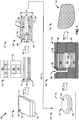
- System 100 may be configured to produce a non-contaminating optical wafer for use in manufacture of the optical article.
- optical lens e.g., a semi-finished (SF) lens product
- a laminate 112 having one or more layers may be provided or formed.
- Each layer of laminate 112 may include a thermoplastic material consolidated (e.g., by pressure and/or temperature) to form a stack.
- laminate 112 includes an inner layer 114 and one or more outer layers 116 that each cover at least a portion of the inner layer.
- a first outer layer e.g., 116
- a second outer layer e.g., 118
- Inner layer 114 and outer layers 116, 118 may be coupled together in any suitable manner such as, for example, via an adhesive layer (e.g., through adhesive lamination, adhesive coating lamination, or the like), without an adhesive layer (e.g., extrusion lamination), or any other known process.
- an adhesive layer e.g., through adhesive lamination, adhesive coating lamination, or the like
- an adhesive layer e.g., extrusion lamination
- Inner layer 114 may include a first matrix material 115.
- first matrix material 115 includes an optically functional thermoplastic elastomeric film such as, for example, a thermoplastic polyurethane (“TPU”) (e.g., amorphous TPU, Tecoflex EG85A, Tecoflex EG80A, Estane ALR E77A-V, Estane AG 8451, Estane VSN F5000, or the like), a semicrystalline Polyether-block-polyamides (PEBA) (e.g., Pebax 5533, Pebax 4533, Pebax 4033, Pellethane 80Aor the like), a soft adhesive layer, or any other thermoplastic elastomeric material.
- TPU thermoplastic polyurethane
- PEBA semicrystalline Polyether-block-polyamides
- one or more additives may be included within matrix material 115.
- an optical additive and/or a process additive e.g., photochromic dye, tint dye, dye absorbers of selective wavelengths, electrochromic dyes, stabilizers, flow modifiers, and/or the like
- an optical additive and/or a process additive can be blended with matrix material 115 to produce an optically functional film (e.g., inner layer 114).
- Outer layers 116, 118 may include a second matrix material 117.
- second matrix material 117 includes a transparent polycarbonate film (e.g., Lexan PC, and/or the like). Second matrix material 117 may have a higher glass transition temperature (or melt temperature) than first matrix material 115.
- a thickness of outer layers 116 may be greater than thickness of inner layer 114 to prevent defects from forming during wafer formation; however, in other implementations, inner layer 114 and outer layers 116, 118 may be sized and shaped in any suitable manner.
- outer layers 116, 118 are described a both having the second matrix material 117, in other implementations, one of the outer layers 116, 118 includes second matrix material and the other of the outer layers 116, 118 includes a third matrix material that is different from the second matrix material.
- Laminate 112 from first stage 110 is provided to a second stage 120 indicated by arrow 119.
- laminate 112 is positioned relative to a tool 122.
- Tool 122 may be configured to remove (e.g., cut) and/or seal a portion of laminate 112.
- tool 122 may be configured to cut a circular or oval shaped disk from laminate 112 that forms a wafer 130.
- Tool 122 includes a cutting apparatus 124 and an imprinting apparatus 126.
- tool 122 may include a uniform body that includes cutting apparatus 124 and imprinting apparatus 126 coupled thereto, while in other implementations, the tool may include multiple district components that include or correspond to cutting apparatus 124 and imprinting apparatus 126.
- tool 122 may include roller (e.g., a cylindrical roller), a planar die, a belt, or other suitable arrangement known in the art.
- Cutting apparatus 124 may use heat, chemicals, force (e.g., cutting edge), or any suitable means to remove wafer 130 from laminate 112.
- cutting apparatus 124 may include a cutting die (e.g., knife die, blanking die,) that cuts an outline pattern (e.g., die pattern) of wafer 130.
- cutting apparatus 124 may include a plurality of circular die cutters having a sharp edge configured to cut a plurality of wafers (e.g., 130) from laminate 112.
- Imprinting apparatus 126 is configured to seal (e.g., via heat and pressure) a portion of laminate 112 and/or wafer 130.
- imprinting apparatus 126 may apply heat and pressure to one or more circular or ring portions of laminate 112 such that at least a portion of one of the layer (e.g., inner layer 114) is displaced.
- imprinting apparatus 126 e.g., heated blunt die
- imprinting apparatus 126 may apply pressure to heated laminate 112 and imprint a shallow annular impression in the laminate sheet to displace a portion of inner layer 114.
- Imprinting apparatus 126 may generate heat at a temperature greater than a glass transition temperature (e.g., melt point) of inner layer 114 and apply pressure to laminate 112 to displace a portion of the inner layer.
- a glass transition temperature e.g., melt point
- wafer 130 may include a reduced thickness of a center TPU layer (e.g., 114) around an outer edge of the wafer.
- imprinting apparatus 126 may generate heat at a temperature less than a glass transition temperature (e.g., melt point) of outer layers 116 such that only a portion of inner layer 114 is displaced by the imprinting apparatus.
- imprinting apparatus 126 may include a plurality of circular hot bands having a dull edge configured to compress a circular portion of wafers (e.g., 130) or laminate 112.
- imprinting apparatus 126 e.g., dull edge
- imprinting apparatus 126 may be shaped to direct the portion of inner layer 114 in a desired direction (as described further with reference to FIG. 3C).
- imprinting apparatus 126 and cutting apparatus 124 cooperate to form wafer 130.
- imprinting apparatus 126 may apply heat and pressure to one or more circular portions of laminate 112 and cutting apparatus 124 may then cut the circular portion(s) to produce a wafer (e.g., 130), as described further herein at least with reference to FIG. 2A .
- cutting apparatus 124 may cut one or more circular portions of laminate 112 to produce wafer 130 and imprinting apparatus 126 may then apply heat and pressure to an outer edge of each wafer 130 to seal an elastomeric layer (e.g., inner layer 114), as described further herein at least with reference to FIG. 4A .
- an elastomeric layer e.g., inner layer 114
- system 100 includes a control device 128, such as a processor and a memory (e.g., a storage device).
- control device 128 may be coupled to or included in tool 122.
- Control device 128 e.g., memory
- model data may include outline data that corresponds to an outline of a wafer 130 that is to be cut from laminate 112.
- tool 122 may be configured receive model data corresponding to a desired shape of wafer 130 and interact with laminate 112 to form the wafer, or a plurality of wafers, according to the model data.
- Laminate 112 from second stage 120 may be formed into one or more wafers 130 provided to a third stage 140 as indicated by an arrow 139.
- third stage 140 an illustrative example of wafer 130 is shown.
- Wafer 130 may include a top surface 132 (e.g., a first surface), a bottom surface 134 (e.g., a second surface) and an outer wall 136.
- Outer wall 136 may extend between top surface 132 and bottom surface 134 of wafer 130.
- outer wall 136 may intersect with top and bottom surfaces to define a periphery of wafer 130.
- top surface 132 and bottom surface 134 include or correspond to the top surface and the bottom surface of laminate 112, respectively.
- wafer 130 may include the same layup (e.g., inner layer 114 and one or more outer layers 116) as described above with reference to laminate 112.
- inner layer 114 may include a lower surface 137 and an upper surface 138 opposite the lower surface.
- a first outer layer e.g., 116
- a second outer layer e.g., 118
- Wafer 130 may be a flat circular disc, however wafer 130 may be sized/shaped in any suitable manner (e.g., elliptical, oval, or otherwise rounded disc) for manufacture of a suitable optical article.
- wafer 130 includes a central portion 142 and an outer edge portion 144.
- Outer edge portion 144 may correspond to a portion of laminate 112 that is contacted by imprinting apparatus 126, at second stage 120.
- wafer 130 includes an imprint 146 (e.g., a recessed portion) at outer edge portion 144.
- outer edge portion 144 includes outer wall 136 that defines a periphery of wafer 130.
- Outer edge portion 144 may surround and cooperate with central portion 142 to define wafer 130.
- outer edge portion 144 and central portion 142 may be concentric portions of wafer 130 with outer edge portion surrounding the central portion.
- central portion 142 includes a first thickness D1 measured from top surface 132 to bottom surface 134 along a straight line that is substantially orthogonal to top and bottom surfaces.
- outer edge portion 144 includes a second thickness D2 measured from top surface 132 to bottom surface 134 along a straight line that is substantially orthogonal to top and bottom surfaces.
- first thickness D1 of central portion 142 of wafer 130 is greater than second thickness D2 of edge portion 144 of the wafer.
- first thickness D1 is greater than second thickness D2 by a distance that is greater than or equal to any of, or between any two of, the following: 0.01, 0.02, 0.03, 0.04, and 0.05, 0.06 or more millimeters (mm).
- inner layer 114 may include a third thickness D3 measured from a top surface (e.g., 138) to a bottom surface (e.g., 137) of inner layer 114 along a straight line (e.g., orthogonal to surface 132) at central portion 142 and a fourth thickness D4 measured from the top surface to the bottom surface of the inner layer along a straight line at outer edge portion 144.
- fourth thickness D4 may correspond to a height of wafer 130 at imprint 146.
- a thickness of inner layer 114 at outer wall 136 may be less than or equal to such that edge bleed (e.g., oozing) of wafer 130 may be reduced or eliminated during formation of the optical article, as described further herein with reference to stage 160.
- edge bleed e.g., oozing
- the outer layers of wafer 130 may be, but need not be, pressed together such that at least a portion a first outer layer (e.g., 116) may contact a portion of a second outer layer (e.g., 118).
- thermoformed wafer 152 may be shaped to include or correspond to a desired lens diameter (e.g., between 60 mm and 100 mm), a desired base curve of the lens or base curve of the mold insert 154 (e.g., between 0.25 and 8.50).
- Wafer 152 includes the same layup as wafer 130.
- inner layer (e.g., 114) of wafer 152 may have a thickness at outer wall 136 that is less than or equal to a thickness of inner layer at a center of wafer 152. In this way, edge defects (e.g., buckling, crease formation, out-of-plane deformation, or the like) at outer wall 136 may be prevented as wafer 130 is heated and shaped to form wafer 152.
- Mold inserts 154, 156 may be sized and shaped such that when they are coupled together, the inserts cooperate to define a cavity 162 that corresponds to a desired shape of optical article 102.
- sidewall 166 of mold block 164 may cooperate with mold inserts 154, 156 to define a portion of cavity 162.
- mold insert 156 may include a convex, concave, or plano surface and mold insert 154 may include a convex, concave, or plano surface having a same, similar, larger or smaller, base curve (e.g., radius of curvature) that define opposing surfaces of a cavity 162.
- Moldable material 148 may include a transparent or semitransparent thermoplastic material, such as polycarbonate, thermoplastic urethane, polyacrylate, polyester, copolyester, polymethacrylate, poly(methyl methacrylate), polystyrene, polyamide, polysulfone, polyphenylsulfone, polyetherimide, polypentene, polyolefin, ionomer, ethylene methacrylic acid, cyclic olefin copolymer, acrylonitrile, styrene maleic anhydride, a copolymer thereof, or a derivative or mixture thereof.
- a transparent or semitransparent thermoplastic material such as polycarbonate, thermoplastic urethane, polyacrylate, polyester, copolyester, polymethacrylate, poly(methyl methacrylate), polystyrene, polyamide, polysulfone, polyphenylsulfone, polyetherimide, polypentene, polyolefin, ion
- Moldable material 158 may be heated, into a liquid form, and injected onto wafer 152.
- moldable material 158 is injected at a high temperature (up to 300 C) and high pressure (500-30,000 psi) so that the moldable material takes the form of cavity 162 and can then be cooled to solidify.
- moldable material 158 fuses to wafer 152 to form a semi-finished optical article (e.g., 102).
- Injection of moldable material 158 onto wafer 152 may cause one of the layers (e.g., 114, 116) of the wafer to transform into a low viscous (e.g., liquid) state.
- moldable material 158 may be injected at a temperature that is much greater than a glass transition temperature of at least one layer (e.g., thermoplastic elastomeric layer) of wafer 152.
- the molten material (e.g., 158) injected into cavity 162 may be injected at a temperature that is greater than the glass transition of matrix material 115 of inner layer 114 such that the inner layer becomes fluid (e.g., a low viscous liquid) and is capable of flowing out under pressure (i.e., oozing out) from wafer 152 onto a surface that defines cavity 162 or between an outer side surface of inserts (e.g., 154, 156) and the walls of the mold block.
- fluid e.g., a low viscous liquid
- the reduced thickness of inner layer 114 at outer wall 136 prevents matrix material 115 from bleeding out from the outer wall of wafer 152.
- the thickness D4 of inner layer 114 at outer edge portion 144 limits and/or prevents movement of inner layer 114 at outer wall 136.
- matrix material 115 may be prevented from oozing from wafer 152 or may be slowed such that moldable material 158 is able to contact outer wall 136 before matrix material oozes from the wafer.
- moldable material 158 may reach outer wall 136 and encapsulate any liquefied material that oozes out from inner layer 114 of wafer 152 to prevent the liquefied material from contaminating the mold inserts 154, 156 the mold block 164, and/or the space between outer side surfaces of the inserts and sidewall 166.
- wafer 152 may reduce or eliminate contamination of one or more components (e.g., mold insert 154, mold receiver 156) of system 100, thus allowing easy removal of inserts from the mold block and otherwise decreasing manufacturing time of optical article.
- Wafer 152 and moldable material 158 are provided to a sixth stage 170 as indicated by an arrow 169.
- wafer 152 and moldable material 158 are removed from cavity 162 after solidifying.
- one or more finishing processes may, but need not be, performed on to wafer 152 and moldable material 158 to form optical article 102.
- optical article 102 may be subjected to a finishing process, such as, for example, coating, stamping, printing, grinding, polishing, buffing, etching, edging, machining, or another process may occur to produce a finished optical article.
- wafer 142 and moldable material 156 are post processed (e.g., edged) to form a shaped lens, however, in other implementations, article 102 will contain a similar shape as cavity 154 (e.g., rounded). As wafer 152 did not contaminate mold inserts 154, 156 or mold block 164, the inserts may be easily removed from the mold block and a second wafer (e.g., 152) may be placed within cavity 162 and a second optical article (e.g., 102) may be formed without cleaning.
- a second wafer e.g., 152
- a second optical article e.g., 102
- control device 128 includes a processor 127 and memory 129.
- Memory 129 may include read only memory (ROM) devices (e.g., programmable read-only memory (PROM), erasable programmable read-only memory (EPROM), electrically erasable programmable read-only memory (EEPROM), optical storage, or the like), random-access memory (RAM) devices (e.g., synchronous RAM (SRAM), dynamic RAM (DRAM), synchronous dynamic RAM (SDRAM), or the like), one or more HDDs, flash memory devices, SSDs, other devices configured to store data in a persistent or non-persistent state, or a combination of different memory devices.
- ROM read only memory
- PROM programmable read-only memory
- EPROM erasable programmable read-only memory
- EEPROM electrically erasable programmable read-only memory
- RAM random-access memory
- HDDs high-volatile memory
- flash memory devices e.g., flash memory devices, SSDs, other devices
- Memory 129 may store instructions that, when executed by processor 127, cause processor 127 to perform, initiate, and/or control the operations described herein.
- control device 128 can include application specific integrated circuits (ASIC), field-programmable gate arrays (FPGA), very large scale integrated (VLSI) circuits, or other circuitry.
- control device 128 may include an interface, such as a wired interface or a wireless interface, to enable communication with one or more components of system 100.
- Control device 128 may also include a user interface to enable a user to control operations of system 100.
- Control device 128 may be configured to control operations of one or more components of system 100.
- control device 128 may control one or more of cutting apparatus 124 and/or imprinting apparatus 126, such as by setting temperatures or pressures applied by cutting apparatus 124 and/or imprinting apparatus 126.
- control device 128 may control operation of one or more actuators (not shown) to cause movement (e.g., translation, rotation, and/or the like) of laminate 112, cutting apparatus 124, and/or imprinting apparatus 126. In this way, tool 122, or components thereof, may be operated to engage with laminate 112 to produce wafer 130.
- control device 128 may include multiple devices or processors (e.g., a processor system) that perform the control operations.
- control device 128 may be a distributed system with multiple processors that each perform some of the control operations described herein.
- a first device or processor may control operation of cutting apparatus 124 and a second device or processor may control operation of imprinting apparatus 126.
- tool 122 for sealing a wafer with a thermoplastic layer for use in an optical article.
- tool 122 includes imprinting apparatus 126 having a first insert and second insert operable during a sealing operation to apply heat, pressure, or both to wafer 130 and reduce a thickness (D4) of layer 114 of the wafer positioned between the first insert and the second insert.
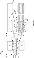
- FIG. 2A-2D aspects for producing an optical wafer-for use in manufacture of an optical article-by a first process are shown.
- FIG. 2A shows a illustrative diagram of a system 200 for producing a wafer 230 used manufacturing an optical article
- FIG. 2B shows an illustrative view of a tool that includes a cutting apparatus 224 and an imprinting apparatus 226,
- FIG. C are cross-sectional views of various examples of imprinting apparatus 226,
- FIG. 2D are cross-sectional views of various examples of cutting apparatus 224.
- System 200 may include or correspond to system 100.
- wafer 230 may include or correspond to wafer 130.
- Cutting apparatus 224 may include one or more protrusions 270 configured to interact with laminate 212 to remove a portion (e.g., wafer 230) of the laminate.
- protrusions 270 may include a surface (e.g., annular surface) having a sharp edge 272.
- each protrusions 270 may include a diameter that is substantially equal to the diameter of the protrusion (e.g., 260) of imprinting apparatus.
- a width of protrusions 260 may be greater than or equal to a width of protrusions 270 to create imprints 246 with sufficient width to allow sharp edge 272 to cut through this region and leave outer wall 236 of wafer 230 with little-to-no TPU film.
- protrusions 260 and protrusions 270 may include any geometry (e.g., circular, oval, square, rectangular, triangular) and may, but need not, include a pattern along the inside or outside of its circumference to form one or more structural features of wafer 230 such as, for example, a tab, a spur, a notch, combination thereof, or the like.
- plate 225 allows imprinting apparatus 226 and cutting apparatus 224 to contact the same portion of laminate 212 during wafer formation.
- plate 225 is shown having a single row for imprinting and a single row for cutting, plate 225 may include a plurality of respective imprinting and cutting rows to increase the manufacturing time of wafer 230.
- cutting apparatus 224 and imprinting apparatus 226 are disposed on a single plate (e.g., 225), in other implementations, tool 222a may include multiple plates (e.g., 225) each having a cutting apparatus (e.g., 224) and/or an imprinting apparatus (e.g., 226).
- tool 222b includes a cylindrical roller 223 that is coupled to, or includes, cutting apparatus 224 and imprinting apparatus 226.
- roller 223 may include a first row of a plurality of heated blunt dies (e.g., 260) positioned along a length of the roller and a second row of a plurality of die cutters (e.g., 270) positioned along the length of the roller.
- Roller 223 may be sized to span a width or a length of laminate 212 and can be rolled along the laminate to create a plurality of imprints using heated blunt dies (e.g., 260) and then further rolled along the laminate to cut the laminate at the plurality of imprints using die cutters (e.g., 270). As shown, cutting apparatus 224 and imprinting apparatus 226 are disposed on a single roller (e.g., 223).
- wafers formed using roller tool 222b may include a thickness (e.g., D4 of inner layer 114) at outer edge portion 244 that is less than a thickness (e.g., D3 of inner layer 114) at central portion 242 to reduce or eliminate edge bleed.
- imprinting apparatus 126 is in contact with laminate 212 for a sufficient time at a sufficient temperature for the heat to reduce the viscosity of the center TPU layer (e.g., 114) so that it will flow when compressed.
- system 200 may include wafer 230 for producing an optical article (e.g., 102).
- wafer 230 includes laminate 212 having first layer 214 and second layer 216.
- first layer 214 includes first matrix material 215 having lower surface 237 and upper surface 238 opposite lower surface 237.
- second layer 216 includes second matrix material 217, and second layer 216 is coupled to first layer 214 and covers at least a portion of lower surface 237 or upper surface 238.
- system 200 may be operable for forming an optical wafer.
- system 200 includes imprinting apparatus 226 configured to imprint an outline of a wafer (e.g., 230) on laminate sheet 212 and cutting apparatus 224 configured to cut wafer 230 from laminate sheet 212.
- imprinting apparatus 226 includes a sealing band (e.g., 260) configured to heat and compress an edge portion (e.g., 244) of the wafer.
- the sealing band 260 may define an angled surface configured to direct a portion of a thermoplastic layer (e.g., 214) of the wafer from the edge portion (e.g., 144) of the wafer.
- FIG. 3A and 3B cross-sectional views of one or more components of an imprinting apparatus and a cutting apparatus are shown.
- FIG. 3A shows a sectional views of protrusions 360a-d of the imprinting apparatus having different dull edges 362a-d (e.g., pressing edges)
- FIG. 3B shows a sectional view of protrusions 370a-c of the cutting apparatus having different sharp edges 372a-c (e.g., cutting edges).
- Imprinting apparatus and cutting apparatus may include or correspond to imprinting apparatus 226, 126 and cutting apparatus 224, 124, respectively.
- Imprinting apparatus is configured to engage a portion of a laminate to apply heat and/or pressure to reduce a thickness (e.g., D2) of the portion of the laminate.
- imprinting apparatus may contact the laminate (e.g., 112, 212) for a sufficient time and at a sufficient pressure and/or temperature to reduce the viscosity of a center TPU layer (e.g., 114) and displace a portion of the center TPU layer where the imprinting apparatus contacts the laminate.
- imprinting apparatus may include one or more protrusions 360a-d configured to contact the laminate.
- protrusion 360a includes a dull edge 362a that corresponds to a planar bottom surface of annular body 364a.
- a dull edge may extend from a bottom surface of an annular body to guide a molten layer inside the laminate when contacted by the protrusion.
- protrusion 360b includes an annular body 364b that has a dull edge 362b that is rounded and extends from a bottom surface of the annular body.
- dull edge e.g., 362b
- dull edge 362a, 362b is symmetrical to evenly distribute a viscous layer of the laminate.
- dull edge is asymmetrical to direct a molten layer in a certain direction.
- protrusion 360c includes an annular body 364c having a dull edge 362c that is angled toward an outer surface of annular body 364c to guide a molten layer away from a center of protrusion 360c.
- Dull edge 362c includes a straight portion that is angled away from protrusion 360c, while in other implementations, a protrusion 360d includes an annular body 364d having a dull edge 362d that is curved toward an outer surface of annular body 364d.
- each protrusion 370a-c may include a corresponding annular body 374a-c and a corresponding sharp edge 372a-c that is configured to cut through at least a portion of a laminate.
- Each sharp edge 372a-c may be sized such that a contact point of the sharp edge provides sufficient pressure to pierce the laminate.
- protrusion 370a may include an annular body 374a having a sharp edge 372a that extends from a bottom surface of annular body 374a. Sharp edge 372a is symmetrical to cut a portion of the laminate.
- sharp edge 372b, 372c may be asymmetrical to achieve a particular purpose such as, for example, creating angled wafers, cutting through specific multi-layer laminate constructions(e.g., sort, hard, or combination), or other suitable purpose known in the art.
- protrusion 370b includes an annular body 374b having a sharp edge 372b that is angled relative to the bottom surface of annular body 374b
- protrusion 370c includes an annular body 374c having a sharp edge 372c that is angled toward an outer surface of annular body 374c. While depicted in conjunction with annular body 374a-c, sharp edges 372a-c may be coupled to any other suitable component of cutting apparatus with similar functionality.
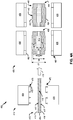
- FIG. 4A-4C aspects of producing an optical wafer-for use in manufacture of an optical article- by a second process is shown.
- FIG. 4A shows an illustrative diagram of a system 400 for producing a wafer 430 used in manufacturing an optical article (e.g., 102)
- FIG. 2B shows a perspective view of an example of an imprinting apparatus 426 used in system 400
- FIG. 4C shows a cross-sectional view of imprinting apparatus 426 in use with a wafer 430.
- Laminate 412, inner layer 414, and outer layers 416 may include or correspond to laminate 112, 212, inner layer 114, 214, and outer layers 116, 118, respectively.
- Inner layer 414 may include a lower surface 437 and an upper surface 438.
- laminate 412 may be disposed between opposing components of cutting apparatus 424.
- cutting apparatus 424 may be positioned either above or below laminate 412.
- Cutting apparatus 424 may include one or more protrusions 470 configured to interact with laminate 412 to remove a portion (e.g., wafer 430) of the laminate.
- protrusions 470 may include a surface (e.g., annular surface) having a sharp edge 472 configured to pierce laminate 412 to remove one or more wafers 430 from the laminate.
- protrusions 470 may include or correspond to cutting apparatus 124 and/or protrusion 370a-c.
- Wafer 430 may include or correspond to wafer 130, and may include a top surface 432, a bottom surface 434, an outer wall 436, a central portion 442 and an outer edge portion 444 that include or correspond to top surface 132, bottom surface 134, outer wall 136, central portion 142 and outer edge portion 144, respectively.
- wafers 430 produced by cutting apparatus 424 are circular, but may be any suitable geometry, such as polygonal (e.g., square, rectangular, hexagonal, octagonal, and/or the like), circular, elliptical, an irregular shape, a combination thereof, and/or the like.
- Wafers 430 from first stage 410 are provided to a second stage 420 indicated by arrow 419.
- laminate 112 is positioned relative to an imprinting apparatus 426 that is configured to interact (e.g., via heat and pressure) with wafer 230 to reduce a thickness of a portion (e.g., outer edge portion 444) of the wafer.
- wafers 430 from first stage 410 may be moved from cutting apparatus 424 toward imprinting apparatus 426 at second stage 420 or, alternatively, wafers 430 may remain stationary after interacting with the cutting apparatus 424 and imprinting apparatus 426 may be moved relative to the wafers at second stage 420.
- Imprinting apparatus 426 may be positioned above laminate 412, below the laminate, or both to produce imprints 446 on wafer 430. Imprinting apparatus 426 may be heated and left in contact with wafer 430 for a sufficient time, pressure, and/or temperature to reduce the viscosity of a center TPU layer (e.g., 114) so that it will flow when compressed.
- imprinting apparatus 426 may include one or more protrusions 460 having a dull edge 462 that is configured to contact laminate 412 to reduce a thickness of a portion (e.g., 244) inner layer 214.
- Protrusions 460 may include or correspond to imprinting apparatus 426 and/or protrusions 360a-d.
- Each protrusion 260 may be shaped based on the desired characteristics of wafer 230.
- imprinting apparatus 426 may apply pressure to outer edge portion 444 of wafer 430 to decrease a thickness of the center TPU layer (e.g., 114) to create a seal at outer wall 436 of the wafer.
- edge bleed e.g., oozing
- one or more other process may be used to seal outer wall 436 of wafer 430 to further prevent edge bleed.
- system 400 may include heating outer edge portion 444 to a temperature that is greater than or equal to the temperature of imprinting apparatus 426, ultrasonic welding may be used to seal the top and bottom polycarbonate films (e.g., 416) at outer wall of wafer 430, or the like.
- ultrasonic welding may be used to seal the top and bottom polycarbonate films (e.g., 416) at outer wall of wafer 430, or the like.
- FIGS. 4B and 4C views of an example of imprinting apparatus 426 are shown.
- FIG. 4B shows a perspective view of imprinting apparatus 426
- FIG. 4C shows a cross-sectional view of imprinting apparatus 426.
- imprinting apparatus 426 is configured to engage a single wafer (e.g., 430), however, it should be understood that imprinting apparatus 426 may be configured to seal a plurality of wafers (e.g., 430) to facilitate efficient manufacture of the wafers.
- Imprinting apparatus 426 may include a first insert 480 and a second insert 490 configured to cooperate to seal wafer 430.
- First insert 480 may be configured to receive a first portion of wafer 430 (e.g., from cutting apparatus 424) and second insert 490 may be configured to receive a second portion of the wafer.
- first and second inserts 480, 490 may engage wafer 430 to decrease a thickness of at least one layer (e.g., 414) of wafer 430 to prevent edge bleed during subsequent manufacturing processes.
- First insert 480 includes a first inner surface 481 that defines a cavity 482 configured to receive a portion of wafer 430.
- first inner surface 481 includes a base 483, a first sidewall 484, a second sidewall 486, and a ledge 485 (e.g., a surface) that extends between the first sidewall and the second sidewall.
- First sidewall 484 corresponds to a first diameter D5 and extends from base 483 to define a first portion of cavity 482.
- Second sidewall 486 corresponds to a second diameter D6 that is greater than first diameter D5 to form ledge 485 that extends laterally between first and second sidewalls 484, 486.
- second insert 490 is able to be disposed within the portion of cavity 482 defined by second sidewall 486 and may apply pressure to wafer 430 at outer edge portion 444 of top surface 132 to reduce a thickness of at least one layer of the wafer at the outer edge portion 444.
- first insert 480 and second insert 490 may be positionable to seal a central TPU layer (e.g., 114) and prevent edge bleed during subsequent manufacturing processes.
- system 400 may include a wafer (e.g., 130,430) for producing an optical article (102).
- the wafer e.g., 430
- the wafer includes a laminate 412 having a first layer (e.g., 414) and a second layer (e.g., 416).
- first layer includes first matrix material 415 having lower surface 437 and upper surface 438 opposite the lower surface 437.
- second layer e.g., 416) includes second matrix material 417, and the second layer is coupled to the first layer and covers at least a portion of lower surface 437 or upper surface 438.
- first thickness e.g., D3 at a central portion (e.g., 442) of the first layer (e.g., 414) that is greater than a second thickness (e.g., D4) at an edge portion (e.g., 444) of the first layer.
- a glass transition temperature of first matrix material 415 is lower than a glass transition temperature of second matrix material 417.
- first matrix material 415 includes a thermoplastic polyurethane (TPU) resin material.
- Laminate 412 includes a third layer (e.g., 418) having a third matrix material.
- second layer covers at least a portion of lower surface 437 of first layer (e.g., 414) and third layer (e.g., 418) is coupled to the first layer(e.g., 414) and covers at least a portion of upper surface 438.
- system 400 may be operable for forming an optical wafer (e.g., 102).
- system 400 includes cutting apparatus 424 configured to cut a wafer (e.g., 430) from laminate 412, such as a laminate sheet, and imprinting apparatus 426 configured to imprint the wafer.
- imprinting apparatus 426 includes a sealing band (e.g., 260, 362a-d, 460) configured to heat and compress an edge portion (e.g., 444) of the wafer.
- the sealing band may define an angled surface configured to direct a portion of a thermoplastic layer (e.g., 414) of the wafer from the edge portion (e.g., 144) of the wafer.
- Second inner surface 491 defines a second opening of a second cavity (e.g., 492) configured to receive a second portion of a wafer.
- first insert 480 and second insert 490 are configured to apply heat, pressure, or both to the wafer and reduce a thickness of a layer (e.g., 114) of the wafer (e.g., 430) positioned between first inner surface 481 of first insert 480 and second inner surface 491 of second insert 490.
- first inner surface 481 defines or includes first sidewall 484 corresponding to a first diameter (e.g., D5) and second sidewall 486 corresponding to second diameter (e.g., D6) that is greater than the first diameter.
- ledge 485 extends between first sidewall 484 and second sidewall 486.
- second inner surface 491 defines or includes third sidewall 494 corresponding to a third diameter (e.g., D7) that is substantially equal to the first diameter (e.g., D5).
- Second insert 490 further includes outer surface 495 that corresponds to a fourth diameter (e.g., D8) that is substantially equal to the second diameter (e.g., D7).
- first surface 432 of the wafer is in contact with ledge 485 and the first and second inserts 480, 490 are configured to compress an outer edge portion (e.g., 444) of the wafer (e.g., 430) to reduce the thickness of the layer of the wafer at the outer edge portion.
- an outer edge portion e.g., 444 of the wafer (e.g., 430) to reduce the thickness of the layer of the wafer at the outer edge portion.
Landscapes
- Engineering & Computer Science (AREA)
- Mechanical Engineering (AREA)
- Health & Medical Sciences (AREA)
- Ophthalmology & Optometry (AREA)
- Manufacturing & Machinery (AREA)
- Physics & Mathematics (AREA)
- General Physics & Mathematics (AREA)
- Optics & Photonics (AREA)
- Chemical & Material Sciences (AREA)
- General Health & Medical Sciences (AREA)
- Microelectronics & Electronic Packaging (AREA)
- Chemical Kinetics & Catalysis (AREA)
- Medicinal Chemistry (AREA)
- Polymers & Plastics (AREA)
- Organic Chemistry (AREA)
- Shaping Of Tube Ends By Bending Or Straightening (AREA)
- Moulds For Moulding Plastics Or The Like (AREA)
- Casting Or Compression Moulding Of Plastics Or The Like (AREA)
Abstract
Description
- The present disclosure relates generally to optical article and, more particularly but without limitation, to the manufacture of optical articles for use with an eyewear apparatus.
- Optical articles, such as lenses, are typically made by functional wafers. Theses wafers may be subject to various manufacturing processes during the formation of an optical article. For example, flat wafers are typically transformed (e.g., thermoformed) from a flat circular wafer to a concave dome-shaped functional wafer to correspond to a base curve of the optical article. The thermoformed functional wafers are then often used in an injection overmolding process to produce corrective or non-corrective eyeglass lenses. Often, the wafer includes a thick center layer of soft thermoplastic material (e.g., soft thermoplastic layer or soft adhesive layer) as it offers certain advantages, such as soft polymer segment, ductility, and chemical compatibility during the formation of the wafers and optical articles. However, there are several complications that arise from using the soft thermoplastic layer in both thermoforming and injection molding processes.
- To illustrate, to maintain the desired ductility of the wafer, the soft thermoplastic layer of the wafer typically has a glass transition temperature well below that of the injection molding temperature that results in outflow (e.g., edge bleeding) of the soft layer. This edge bleeding creates unwanted contamination of the insert, mold cavity and/or space between the outer side surface of the insert and the mold cavity walls. This contamination may prevent removal of the insert from the mold block and/or create buildup of unwanted material on the molding surfaces which affects product yields, increases down time due to mold cleaning, and leads to imperfections in subsequent lens formation such as, for example, non-uniform thickness of the soft thermoplastic layer which may result in optical distortions or cosmetic issues in the lenses. Some conventional approaches to preventing edge bleeding have included using outer layers that have a larger diameter than the soft, central layer to prevent the central layer from bleeding into the mold cavity. However, such wafer geometry is difficult to produce on a large scale and the soft layer is still visible after injection molding. Accordingly, such solutions offer little help in reducing manufacturing time and produce lenses with undesirable cosmetic properties.
- The present disclosure is generally related to systems, devices, and methods for manufacturing an optical article. For example, a method of manufacturing an optical article may include sealing and cutting a laminate to form a functional wafer. Sealing the laminate may include liquefying at least a portion of a thermoplastic layer of a laminate and displacing the liquefied portion of the thermoplastic layer to produce a wafer having an inner layer that includes a central portion having a first thickness that is greater than a second thickness at an edge portion of the inner layer. The reduced thickness of the inner layer at the edge portion of the wafer may prevent molten material from bleeding out of the wafer during subsequent manufacturing steps to produce the optical article. In another example, a system may include one or more tools for producing a non-contaminating optical wafer for use in manufacture of the optical article. The one or more tools may include an imprinting apparatus and a cutting apparatus. To illustrate, the imprinting apparatus is configured to form an imprint in the laminate and the cutting apparatus is configured to cut out wafers from the laminate. In this way, imprinting apparatus and cutting apparatus may operate in conjunction to efficiently produce a plurality of non-contaminating wafers in a timely and reproducible manner. In some implementations, the imprinting apparatus may operate on a laminate prior to operation of the cutting apparatus on the laminate. In other implementations, the cutting apparatus may operate on a laminate to form a wafer prior to an operation of the imprinting apparatus on the wafer. Consequently, the disclosed system, apparatuses, and methods enable mass production of a non-contaminating optical wafer capable of preventing edge bleed and subsequent contamination of the mold cavity without sacrificing the cosmetic appearance of the lenses.
- In some of the foregoing implementations of the present methods (e.g., of forming a wafer for use in an optical article), a method includes liquefying at least a portion of a thermoplastic layer of a laminate. The method also includes displacing the liquefied portion of the thermoplastic layer. The method further includes cutting a wafer from the laminate. In some such implementations, liquefying the at least the portion of the thermoplastic layer of the laminate may include heating the at least the portion of a thermoplastic layer of the laminate. Additionally, or alternatively, cutting the wafer may include cutting the laminate to define an outer edge of the wafer.
- In some such implementations of the present methods, cutting the wafer may occurs subsequent to displacing the liquefied portion of the thermoplastic layer. Additionally, or alternatively, displacing the liquefied portion of the thermoplastic layer may include compressing the portion of the thermoplastic layer of the laminate. In some implementations, compressing the portion of the thermoplastic layer of the laminate may displace the liquefied portion in a direction outward from a center of the wafer.
- In some such implementations of the present methods, the method further includes sealing a sidewall of the wafer. Additionally, or alternatively, cutting the wafer from the laminate may occur prior to liquefying the at least the portion of a thermoplastic layer of the laminate. In some implementations, the method may also include thermoforming the wafer, and placing the thermoformed wafer into a mold cavity to form an optical article.
- In some of the foregoing implementations of the present apparatuses (e.g., wafers of an optical article), a wafer includes a laminate. The laminate includes a first layer and a second layer. The first layer includes a first matrix material having a lower surface and an upper surface opposite the lower surface. The second layer includes a second matrix material and the second layer is coupled to the first layer and covers at least a portion of the lower surface or the upper surface. A first thickness at a central portion of the first layer that is greater than a second thickness at an edge portion of the first layer. In some such implementations, a glass transition temperature of the first matrix material may be lower than a glass transition temperature of the second matrix material. Additionally, or alternatively, the first matrix material may include a thermoplastic polyurethane (TPU) resin material.
- In some such implementations of the present apparatuses, the second layer covers at least a portion of the lower surface. Additionally, or alternatively, the laminate may further include a third layer having a third matrix material. For example, the third layer may be coupled to the first layer and cover at least a portion of the upper surface. In some implementations, the second matrix material, the third matrix material, or both the second and third matric materials include polycarbonate.
- In some of the foregoing implementations of the present systems (e.g. for forming an optical wafer), a system includes an imprinting apparatus configured to imprint an outline of a wafer on a laminate sheet. The imprinting apparatus includes a sealing band configured to heat and compress an edge portion of a wafer. The system further includes a cutting apparatus configured to cut the wafer from the laminate sheet. In some such implementations, the sealing band may define an angled surface that is configured to direct a portion of a thermoplastic layer of the wafer from the edge portion of the wafer.
- In some such implementations of the present systems, the sealing band is configured to define an annular imprint in the laminate sheet. The annular imprint may have a first diameter. Additionally, or alternatively, the cutting apparatus may include a die cutter configured to cut through the laminate sheet at the annular imprint to define an edge surface of the wafer.
- In some of the foregoing implementations of the present apparatuses (e.g., tools for sealing a wafer with a thermoplastic layer for use in an optical article), a tool includes a first insert and a second insert. The first insert includes a first inner surface configured to contact a first surface of a wafer. The first inner surface defines a first opening of a first cavity configured to receive a first portion of a wafer. The second inner surface is configured to contact a second surface of the wafer. The second inner surface defines a second opening of a second cavity configured to receive a second portion of a wafer. During a sealing operation, the first insert and the second insert are configured to: apply heat, pressure, or both to the wafer; and reduce a thickness of a layer of the wafer positioned between the first inner surface of the first insert and the second inner surface of the second insert.
- In some such implementations of the present apparatuses, the first inner surface defines: a first sidewall having a first diameter; a second sidewall having a second diameter that is greater than the first diameter; and a ledge extends between the first sidewall and the second sidewall. Additionally, or alternatively, the second inner surface may define a third sidewall having a third diameter that is substantially equal to the first diameter. In some such implementations, the second insert may further include an outer surface that has a fourth diameter that is substantially equal to the second diameter. In some implementations, during the sealing operation: the first surface of the wafer is in contact with the ledge; and the first and second insert are configured to compress an outer edge portion of the wafer to reduce the thickness of the layer of the wafer at the outer edge portion.
- As used herein, various terminology is for the purpose of describing particular implementations only and is not intended to be limiting of implementations. For example, as used herein, an ordinal term (e.g., "first," "second," "third," etc.) used to modify an element, such as a structure, a component, an operation, etc., does not by itself indicate any priority or order of the element with respect to another element, but rather merely distinguishes the element from another element having a same name (but for use of the ordinal term). The term "coupled" is defined as connected, although not necessarily directly, and not necessarily mechanically; two items that are "coupled" may be unitary with each other. The terms "a" and "an" are defined as one or more unless this disclosure explicitly requires otherwise. The term "substantially" is defined as largely but not necessarily wholly what is specified (and includes what is specified; e.g., substantially 90 degrees includes 90 degrees and substantially parallel includes parallel), as understood by a person of ordinary skill in the art. In any disclosed implementations, the term "substantially" may be substituted with "within [a percentage] of' what is specified, where the percentage includes .1, 1, 5, and 10 percent.
- The term "about" as used herein can allow for a degree of variability in a value or range, for example, within 10%, within 5%, or within 1% of a stated value or of a stated limit of a range and includes the exact stated value or range. The term "substantially" is defined as largely but not necessarily wholly what is specified (and includes what is specified; e.g., substantially 90 degrees includes 90 degrees and substantially parallel includes parallel), as understood by a person of ordinary skill in the art. In any disclosed implementation, the term "substantially" may be substituted with "within [a percentage] of' what is specified, where the percentage includes 0.1, 1, or 5 percent; and the term "approximately" may be substituted with "within 10 percent of' what is specified. The statement "substantially X to Y" has the same meaning as "substantially X to substantially Y," unless indicated otherwise. Likewise, the statement "substantially X, Y, or substantially Z" has the same meaning as "substantially X, substantially Y, or substantially Z," unless indicated otherwise. The phrase "and/or" means and or or. To illustrate, A, B, and/or C includes: A alone, B alone, C alone, a combination of A and B, a combination of A and C, a combination of B and C, or a combination of A, B, and C. In other words, "and/or" operates as an inclusive or. Additionally, the phrase "A, B, C, or a combination thereof' or "A, B, C, or any combination thereof' includes: A alone, B alone, C alone, a combination of A and B, a combination of A and C, a combination of B and C, or a combination of A, B, and C.
- Throughout this document, values expressed in a range format should be interpreted in a flexible manner to include not only the numerical values explicitly recited as the limits of the range, but also to include all the individual numerical values or sub-ranges encompassed within that range as if each numerical value and sub-range is explicitly recited. For example, a range of "about 0.1 % to about 5%" or "about 0.1 % to 5%" should be interpreted to include not just about 0.1 % to about 5%, but also the individual values (e.g., 1 %, 2%, 3%, and 4%) and the sub-ranges (e.g., 0.1 % to 0.5%, 1.1 % to 2.2%, 3.3% to 4.4%) within the indicated range. The terms "comprise" (and any form of comprise, such as "comprises" and "comprising"), "have" (and any form of have, such as "has" and "having"), and "include" (and any form of include, such as "includes" and "including") are open-ended linking verbs. As a result, an apparatus that "comprises," "has," or "includes" one or more elements possesses those one or more elements, but is not limited to possessing only those one or more elements. Likewise, a method that "comprises," "has," or "includes" one or more steps possesses those one or more steps, but is not limited to possessing only those one or more steps.
- Any implementation of any of the systems, methods, and article of manufacture can consist of or consist essentially of - rather than comprise/have/include - any of the described steps, elements, and/or features. Thus, in any of the claims, the term "consisting of' or "consisting essentially of' can be substituted for any of the open-ended linking verbs recited above, in order to change the scope of a given claim from what it would otherwise be using the open-ended linking verb. Additionally, the term "wherein" may be used interchangeably with "where". Further, a device or system that is configured in a certain way is configured in at least that way, but it can also be configured in other ways than those specifically described. The feature or features of one implementation may be applied to other implementations, even though not described or illustrated, unless expressly prohibited by this disclosure or the nature of the implementations.
- Some details associated with the implementations are described above, and others are described below. Other implementations, advantages, and features of the present disclosure will become apparent after review of the entire application, including the following sections: Brief Description of the Drawings, Detailed Description, and the Claims.
- The following drawings illustrate by way of example and not limitation. For the sake of brevity and clarity, every feature of a given structure is not always labeled in every figure in which that structure appears. Identical reference numbers do not necessarily indicate an identical structure. Rather, the same reference number may be used to indicate a similar feature or a feature with similar functionality, as may non-identical reference numbers. The figures are drawn to scale (unless otherwise noted), meaning the sizes of the depicted elements are accurate relative to each other for at least the configuration depicted in the figures.
-
FIG. 1 is a diagram that illustrates an example of stages of a process of an optical system for manufacturing an optical article. -
FIG. 2A is another diagram that illustrates an example of a first process for producing a wafer used manufacturing an optical article. -
FIG. 2B an illustrative view of an example of a first tool that includes a cutting apparatus and an imprinting apparatus of the optical system. -
FIG. 2C an illustrative view of an example of a second tool that includes a cutting apparatus and an imprinting apparatus of the optical system. -
FIG. 3A is a cross-sectional view of various examples of an imprinting apparatus of the optical system. -
FIG. 3B is a cross-sectional view of various examples of a cutting apparatus of the optical system. -
FIG. 4A is another diagram that illustrates an example of a second process for producing a wafer used manufacturing an optical article. -
FIG. 4B is a perspective view of an example of a sealing apparatus of the optical system. -
FIG. 4C is a side cross-sectional view of the sealing apparatus ofFIG. 4B . -
FIG. 5 is a flowchart illustrating an example of a method of forming a wafer of the optical system. - Referring to
FIG. 1 , a diagram of illustrative stages of a system for manufacturing an optical article, such as an optical lens (e.g., a semi-finished (SF) lens product), is shown and generally designated 100.System 100 may be configured to produce a non-contaminating optical wafer for use in manufacture of the optical article. - At a
first stage 110, a laminate 112 having one or more layers may be provided or formed. Each layer oflaminate 112 may include a thermoplastic material consolidated (e.g., by pressure and/or temperature) to form a stack. As shown inFIG. 1 ,laminate 112 includes aninner layer 114 and one or moreouter layers 116 that each cover at least a portion of the inner layer. For example, a first outer layer (e.g., 116) may be disposed on a top surface ofinner layer 114 and a second outer layer (e.g., 118) may be disposed on a bottom surface of the inner layer.Inner layer 114 andouter layers -
Inner layer 114 may include afirst matrix material 115. In some implementations,first matrix material 115 includes an optically functional thermoplastic elastomeric film such as, for example, a thermoplastic polyurethane ("TPU") (e.g., amorphous TPU, Tecoflex EG85A, Tecoflex EG80A, Estane ALR E77A-V, Estane AG 8451, Estane VSN F5000, or the like), a semicrystalline Polyether-block-polyamides (PEBA) (e.g., Pebax 5533, Pebax 4533, Pebax 4033, Pellethane 80Aor the like), a soft adhesive layer, or any other thermoplastic elastomeric material. In some implementations, one or more additives may be included withinmatrix material 115. For example, an optical additive and/or a process additive (e.g., photochromic dye, tint dye, dye absorbers of selective wavelengths, electrochromic dyes, stabilizers, flow modifiers, and/or the like) can be blended withmatrix material 115 to produce an optically functional film (e.g., inner layer 114). -
Outer layers second matrix material 117. In some implementations,second matrix material 117 includes a transparent polycarbonate film (e.g., Lexan PC, and/or the like).Second matrix material 117 may have a higher glass transition temperature (or melt temperature) thanfirst matrix material 115. In some implementations, a thickness ofouter layers 116 may be greater than thickness ofinner layer 114 to prevent defects from forming during wafer formation; however, in other implementations,inner layer 114 andouter layers outer layers second matrix material 117, in other implementations, one of theouter layers outer layers -
Laminate 112 fromfirst stage 110 is provided to asecond stage 120 indicated by arrow 119. Atsecond stage 120,laminate 112 is positioned relative to atool 122.Tool 122 may be configured to remove (e.g., cut) and/or seal a portion oflaminate 112. For example,tool 122 may be configured to cut a circular or oval shaped disk fromlaminate 112 that forms awafer 130. -
Tool 122 includes acutting apparatus 124 and animprinting apparatus 126. In some implementations,tool 122 may include a uniform body that includes cuttingapparatus 124 andimprinting apparatus 126 coupled thereto, while in other implementations, the tool may include multiple district components that include or correspond to cuttingapparatus 124 andimprinting apparatus 126. For example,tool 122 may include roller (e.g., a cylindrical roller), a planar die, a belt, or other suitable arrangement known in the art. -
Cutting apparatus 124 may use heat, chemicals, force (e.g., cutting edge), or any suitable means to removewafer 130 fromlaminate 112. For example, cuttingapparatus 124 may include a cutting die (e.g., knife die, blanking die,) that cuts an outline pattern (e.g., die pattern) ofwafer 130. For example, cuttingapparatus 124 may include a plurality of circular die cutters having a sharp edge configured to cut a plurality of wafers (e.g., 130) fromlaminate 112. -
Imprinting apparatus 126 is configured to seal (e.g., via heat and pressure) a portion oflaminate 112 and/orwafer 130. To illustrate,imprinting apparatus 126 may apply heat and pressure to one or more circular or ring portions oflaminate 112 such that at least a portion of one of the layer (e.g., inner layer 114) is displaced. For example, imprinting apparatus 126 (e.g., heated blunt die) may apply pressure toheated laminate 112 and imprint a shallow annular impression in the laminate sheet to displace a portion ofinner layer 114.Imprinting apparatus 126 may generate heat at a temperature greater than a glass transition temperature (e.g., melt point) ofinner layer 114 and apply pressure to laminate 112 to displace a portion of the inner layer. In this way,wafer 130 may include a reduced thickness of a center TPU layer (e.g., 114) around an outer edge of the wafer. In some such some implementation,imprinting apparatus 126 may generate heat at a temperature less than a glass transition temperature (e.g., melt point) ofouter layers 116 such that only a portion ofinner layer 114 is displaced by the imprinting apparatus. For example,imprinting apparatus 126 may include a plurality of circular hot bands having a dull edge configured to compress a circular portion of wafers (e.g., 130) orlaminate 112. In some implementations, imprinting apparatus 126 (e.g., dull edge) may be shaped to direct the portion ofinner layer 114 in a desired direction (as described further with reference to FIG. 3C). - In some implementations of
system 100,imprinting apparatus 126 and cuttingapparatus 124 cooperate to formwafer 130. To illustrate,imprinting apparatus 126 may apply heat and pressure to one or more circular portions oflaminate 112 and cuttingapparatus 124 may then cut the circular portion(s) to produce a wafer (e.g., 130), as described further herein at least with reference toFIG. 2A . Alternatively, cuttingapparatus 124 may cut one or more circular portions oflaminate 112 to producewafer 130 andimprinting apparatus 126 may then apply heat and pressure to an outer edge of eachwafer 130 to seal an elastomeric layer (e.g., inner layer 114), as described further herein at least with reference toFIG. 4A . - In some implementations,
system 100 includes acontrol device 128, such as a processor and a memory (e.g., a storage device). For example,control device 128 may be coupled to or included intool 122. Control device 128 (e.g., memory) may be configured to store model data, such as two or three dimensional model data ofwafer 130 oroptical article 102. For example, model data may include outline data that corresponds to an outline of awafer 130 that is to be cut fromlaminate 112. In this way,tool 122 may be configured receive model data corresponding to a desired shape ofwafer 130 and interact withlaminate 112 to form the wafer, or a plurality of wafers, according to the model data. -
Laminate 112 fromsecond stage 120 may be formed into one ormore wafers 130 provided to athird stage 140 as indicated by anarrow 139. Atthird stage 140, an illustrative example ofwafer 130 is shown. -
Wafer 130 may include a top surface 132 (e.g., a first surface), a bottom surface 134 (e.g., a second surface) and anouter wall 136.Outer wall 136 may extend betweentop surface 132 andbottom surface 134 ofwafer 130. In some implementations,outer wall 136 may intersect with top and bottom surfaces to define a periphery ofwafer 130. In some implementations,top surface 132 andbottom surface 134 include or correspond to the top surface and the bottom surface oflaminate 112, respectively. For example,wafer 130 may include the same layup (e.g.,inner layer 114 and one or more outer layers 116) as described above with reference tolaminate 112. To illustrate,inner layer 114 may include a lower surface 137 and anupper surface 138 opposite the lower surface. In such implementations, a first outer layer (e.g., 116) is coupled to lower surface 137 ofinner layer 114 and a second outer layer (e.g., 118) is coupled toupper surface 138 of the inner layer.Wafer 130 may be a flat circular disc, howeverwafer 130 may be sized/shaped in any suitable manner (e.g., elliptical, oval, or otherwise rounded disc) for manufacture of a suitable optical article. - In some implementations,
wafer 130 includes acentral portion 142 and anouter edge portion 144.Outer edge portion 144 may correspond to a portion oflaminate 112 that is contacted by imprintingapparatus 126, atsecond stage 120. For example,wafer 130 includes an imprint 146 (e.g., a recessed portion) atouter edge portion 144. In some implementations,outer edge portion 144 includesouter wall 136 that defines a periphery ofwafer 130.Outer edge portion 144 may surround and cooperate withcentral portion 142 to definewafer 130. For example,outer edge portion 144 andcentral portion 142 may be concentric portions ofwafer 130 with outer edge portion surrounding the central portion. In some implementations, each layer (e.g., 114, 116, 118) may include a central portion (e.g., 142) and an outer edge portion (e.g., 144) that correspond to the central portion and outer edge portion, respectively, ofwafer 130. - In the depicted implementation,
central portion 142 includes a first thickness D1 measured fromtop surface 132 tobottom surface 134 along a straight line that is substantially orthogonal to top and bottom surfaces. Additionally,outer edge portion 144 includes a second thickness D2 measured fromtop surface 132 tobottom surface 134 along a straight line that is substantially orthogonal to top and bottom surfaces. In some implementations, first thickness D1 ofcentral portion 142 ofwafer 130 is greater than second thickness D2 ofedge portion 144 of the wafer. For example, first thickness D1 is greater than second thickness D2 by a distance that is greater than or equal to any of, or between any two of, the following: 0.01, 0.02, 0.03, 0.04, and 0.05, 0.06 or more millimeters (mm). - In some implementations, a thickness of at least one of the layers (e.g., 114, 116, 118) of
wafer 130 atouter edge portion 144 is less than a thickness of the least one layer at the central portion. For example, asimprinting apparatus 126 may heatwafer 130,matrix material 115 ofinner layer 114 may be changed into a viscous state and, upon application of pressure, the matrix material subjected to the pressure is displaced, reducing the thickness of a portion (e.g., imprint 146) ofinner layer 114. To illustrate,inner layer 114 may include a third thickness D3 measured from a top surface (e.g., 138) to a bottom surface (e.g., 137) ofinner layer 114 along a straight line (e.g., orthogonal to surface 132) atcentral portion 142 and a fourth thickness D4 measured from the top surface to the bottom surface of the inner layer along a straight line atouter edge portion 144. Atthird stage 140, fourth thickness D4 may correspond to a height ofwafer 130 atimprint 146. In this manner, a thickness ofinner layer 114 at outer wall 136 (e.g., D4) may be less than or equal to such that edge bleed (e.g., oozing) ofwafer 130 may be reduced or eliminated during formation of the optical article, as described further herein with reference tostage 160. In some implementations, the outer layers ofwafer 130 may be, but need not be, pressed together such that at least a portion a first outer layer (e.g., 116) may contact a portion of a second outer layer (e.g., 118). -
Wafer 130 fromthird stage 140 is provided to afourth stage 150 as indicated by anarrow 149. Atfourth stage 150,wafer 130 may be provided to thermoform equipment 151 (e.g., a thermoform chamber) and thermoformed to from aconcave wafer 152 that is configured to fit within a mold insert (e.g., 154, 156). For example,wafer 130 may be thermoformed (e.g., via heat and pressure) to a semi-spherical dome shape suitable for use in making optical lenses. In some implementations,wafer 130 may be thermoformed to generate athermoformed wafer 152 having a concave side and convex side similar to that ofoptical article 102. To illustrate,thermoformed wafer 152 may be shaped to include or correspond to a desired lens diameter (e.g., between 60 mm and 100 mm), a desired base curve of the lens or base curve of the mold insert 154 (e.g., between 0.25 and 8.50).Wafer 152 includes the same layup aswafer 130. For example, inner layer (e.g., 114) ofwafer 152 may have a thickness atouter wall 136 that is less than or equal to a thickness of inner layer at a center ofwafer 152. In this way, edge defects (e.g., buckling, crease formation, out-of-plane deformation, or the like) atouter wall 136 may be prevented aswafer 130 is heated and shaped to formwafer 152. - Wafer 130 (e.g., thermoformed wafer 152) from
fourth stage 150 is provided to afifth stage 160 as indicated by anarrow 159. Atfifth stage 160,wafer 152 may be disposed within amold device 161. Mold device may include a mold inserts 154, 156 and amold block 164. To further illustrate,wafer 152 may be disposed within mold inserts 154, 156 and the mold inserts are subsequently coupled tomold block 164. For example, mold inserts 154, 156 are disposed within a space defined by asidewall 166 ofmold block 164. Mold inserts 154, 156 may be sized and shaped such that when they are coupled together, the inserts cooperate to define acavity 162 that corresponds to a desired shape ofoptical article 102. In some implementations,sidewall 166 ofmold block 164 may cooperate with mold inserts 154, 156 to define a portion ofcavity 162. For example,mold insert 156 may include a convex, concave, or plano surface andmold insert 154 may include a convex, concave, or plano surface having a same, similar, larger or smaller, base curve (e.g., radius of curvature) that define opposing surfaces of acavity 162. - As shown,
moldable material 158 is injected onto thewafer 152 whilewafer 152 is positioned withincavity 162. Moldable material 148 may include a transparent or semitransparent thermoplastic material, such as polycarbonate, thermoplastic urethane, polyacrylate, polyester, copolyester, polymethacrylate, poly(methyl methacrylate), polystyrene, polyamide, polysulfone, polyphenylsulfone, polyetherimide, polypentene, polyolefin, ionomer, ethylene methacrylic acid, cyclic olefin copolymer, acrylonitrile, styrene maleic anhydride, a copolymer thereof, or a derivative or mixture thereof. Moldable material 158 (e.g., matrix material) may be heated, into a liquid form, and injected ontowafer 152. For example,moldable material 158 is injected at a high temperature (up to 300 C) and high pressure (500-30,000 psi) so that the moldable material takes the form ofcavity 162 and can then be cooled to solidify. During cooling,moldable material 158 fuses towafer 152 to form a semi-finished optical article (e.g., 102). Injection ofmoldable material 158 ontowafer 152 may cause one of the layers (e.g., 114, 116) of the wafer to transform into a low viscous (e.g., liquid) state. For example,moldable material 158 may be injected at a temperature that is much greater than a glass transition temperature of at least one layer (e.g., thermoplastic elastomeric layer) ofwafer 152. Specifically, the molten material (e.g., 158) injected intocavity 162 may be injected at a temperature that is greater than the glass transition ofmatrix material 115 ofinner layer 114 such that the inner layer becomes fluid (e.g., a low viscous liquid) and is capable of flowing out under pressure (i.e., oozing out) fromwafer 152 onto a surface that definescavity 162 or between an outer side surface of inserts (e.g., 154, 156) and the walls of the mold block. - In the implementations shown, the reduced thickness of
inner layer 114 at outer wall 136 (e.g., D4) preventsmatrix material 115 from bleeding out from the outer wall ofwafer 152. For example, the thickness D4 ofinner layer 114 atouter edge portion 144 limits and/or prevents movement ofinner layer 114 atouter wall 136. In this manner,matrix material 115 may be prevented from oozing fromwafer 152 or may be slowed such thatmoldable material 158 is able to contactouter wall 136 before matrix material oozes from the wafer. As a result,moldable material 158 may reachouter wall 136 and encapsulate any liquefied material that oozes out frominner layer 114 ofwafer 152 to prevent the liquefied material from contaminating the mold inserts 154, 156 themold block 164, and/or the space between outer side surfaces of the inserts andsidewall 166. Accordingly,wafer 152 may reduce or eliminate contamination of one or more components (e.g.,mold insert 154, mold receiver 156) ofsystem 100, thus allowing easy removal of inserts from the mold block and otherwise decreasing manufacturing time of optical article. -
Wafer 152 andmoldable material 158 are provided to asixth stage 170 as indicated by anarrow 169. Atsixth stage 170,wafer 152 andmoldable material 158 are removed fromcavity 162 after solidifying. In some implementations, one or more finishing processes may, but need not be, performed on towafer 152 andmoldable material 158 to formoptical article 102. For example, in some implementations,optical article 102 may be subjected to a finishing process, such as, for example, coating, stamping, printing, grinding, polishing, buffing, etching, edging, machining, or another process may occur to produce a finished optical article. As shown,wafer 142 andmoldable material 156 are post processed (e.g., edged) to form a shaped lens, however, in other implementations,article 102 will contain a similar shape as cavity 154 (e.g., rounded). Aswafer 152 did not contaminate mold inserts 154, 156 ormold block 164, the inserts may be easily removed from the mold block and a second wafer (e.g., 152) may be placed withincavity 162 and a second optical article (e.g., 102) may be formed without cleaning. - In some implementations,
control device 128 includes aprocessor 127 andmemory 129.Memory 129 may include read only memory (ROM) devices (e.g., programmable read-only memory (PROM), erasable programmable read-only memory (EPROM), electrically erasable programmable read-only memory (EEPROM), optical storage, or the like), random-access memory (RAM) devices (e.g., synchronous RAM (SRAM), dynamic RAM (DRAM), synchronous dynamic RAM (SDRAM), or the like), one or more HDDs, flash memory devices, SSDs, other devices configured to store data in a persistent or non-persistent state, or a combination of different memory devices.Memory 129 may store instructions that, when executed byprocessor 127,cause processor 127 to perform, initiate, and/or control the operations described herein. Although described as includingprocessor 127, in other implementations,control device 128 can include application specific integrated circuits (ASIC), field-programmable gate arrays (FPGA), very large scale integrated (VLSI) circuits, or other circuitry. Additionally,control device 128 may include an interface, such as a wired interface or a wireless interface, to enable communication with one or more components ofsystem 100.Control device 128 may also include a user interface to enable a user to control operations ofsystem 100. -
Control device 128 may be configured to control operations of one or more components ofsystem 100. For example,control device 128 may control one or more of cuttingapparatus 124 and/orimprinting apparatus 126, such as by setting temperatures or pressures applied by cuttingapparatus 124 and/orimprinting apparatus 126. As another example,control device 128 may control operation of one or more actuators (not shown) to cause movement (e.g., translation, rotation, and/or the like) oflaminate 112, cuttingapparatus 124, and/orimprinting apparatus 126. In this way,tool 122, or components thereof, may be operated to engage withlaminate 112 to producewafer 130. - Although described as a single control device (e.g., a single processor), in other implementations,
control device 128 may include multiple devices or processors (e.g., a processor system) that perform the control operations. For example,control device 128 may be a distributed system with multiple processors that each perform some of the control operations described herein. To further illustrate, a first device or processor may control operation of cuttingapparatus 124 and a second device or processor may control operation ofimprinting apparatus 126. - In some implementations,
system 100 may includewafer optical article 102. In some implementations,wafer first layer 114 andsecond layer 116. In such implementations,first layer 114 includesfirst matrix material 115 having a first surface (e.g., lower surface 137) and a second surface (e.g., an upper surface 138) opposite the first surface. First matrix material (e.g., 115) may include a thermoplastic polyurethane (TPU) resin material. In some such implementations,second layer 116 includessecond matrix material 117, and the second layer is coupled to the first layer and covers at least a portion of the first surface or the second surface. A first thickness (D3) at acentral portion 142 offirst layer 114 is greater than a second thickness (D4) atedge portion 144 offirst layer 114. - In some implementations, a glass transition temperature of
first matrix material 115 is lower than a glass transition temperature ofsecond matrix material 117. In some such implementations,laminate 112 may includethird layer 118 which includes a third matrix material. The second matrix material and the third matric material may include the same material or may include different materials.Second layer 116 may cover at least a portion of the first surface (e.g., 137) offirst layer 114. Additionally,third layer 118 may be coupled tofirst layer 114 and cover at least a portion of the second surface (e.g., 138). - In some of the foregoing implementations,
system 100 may be operable for formingoptical wafer 102. For example,system 100 may includeimprinting apparatus 126 configured to imprint an outline ofwafer 130 onlaminate sheet 112 and cuttingapparatus 124 configured to cut a wafer fromlaminate sheet 112. In some such implementations,imprinting apparatus 126 includes a sealing band configured to heat and compressedge portion 144 ofwafer 130. For example, the sealing band may define an angled surface configured to direct a portion ofthermoplastic layer 114 ofwafer 130 fromedge portion 144 ofwafer 130. In some implementations, the sealing band is configured to defineannular imprint 146 inlaminate sheet 112, and cuttingapparatus 124 includes a die cutter configured to cut throughlaminate sheet 112 atannular imprint 146 to defineedge surface 136 ofwafer 130. - As another example, in some implementations,
system 100 may be configured such that cuttingapparatus 124 is configured to cut the wafer from thelaminate sheet 112. In such implementations, imprinting apparatus 126 (or another tool) is configured to imprint an outline ofwafer 130 to form a recessed portion of the wafer. - Some of the foregoing implementations include a
tool 122 for sealing a wafer with a thermoplastic layer for use in an optical article. In some implementations,tool 122 includesimprinting apparatus 126 having a first insert and second insert operable during a sealing operation to apply heat, pressure, or both towafer 130 and reduce a thickness (D4) oflayer 114 of the wafer positioned between the first insert and the second insert. - Thus,
system 100 may includetool 122 that engages laminate 112 to form a wafer (e.g., 130) to reduce or eliminate edge bleed.Tool 122 may include acutting apparatus 124 and/orimprinting apparatus 126 to reduce a thickness of at least one thermoplastic layer of laminate at an outer edge portion (e.g., 144) to prevent contamination during the manufacture of an optical article.Tool 122 may enable mass production of wafers with minimized edge bleed to enable a scalable system for prevention of edge bleeding from thermoplastic based optically functional laminate wafers and subsequent contamination of the mold cavity without sacrificing the cosmetic appearance of the lenses. - Referring now to
FIG. 2A-2D , aspects for producing an optical wafer-for use in manufacture of an optical article-by a first process are shown. For example,FIG. 2A shows a illustrative diagram of asystem 200 for producing awafer 230 used manufacturing an optical article,FIG. 2B shows an illustrative view of a tool that includes acutting apparatus 224 and animprinting apparatus 226, FIG. C are cross-sectional views of various examples ofimprinting apparatus 226, and FIG. 2D are cross-sectional views of various examples of cuttingapparatus 224.System 200 may include or correspond tosystem 100. Additionally,wafer 230 may include or correspond towafer 130. - As shown in
FIG. 2A , at afirst stage 210,laminate 212 is positioned relative toimprinting apparatus 226. Laminate may include aninner layer 214 having afirst matrix material 215 that is disposed between twoouter layers second matrix material 217.Laminate 212,inner layer 214, andouter layers inner layer 114, andouter layers inner layer 214 may include alower surface 237 and anupper surface 238. Althoughouter layers second matrix material 217, in other implementations, one of theouter layers outer layers - As depicted at
first stage 210,laminate 212 may be disposed between opposing components ofimprinting apparatus 226. However, in in other implementations, imprinting apparatus may be positioned either above or belowlaminate 212 to produce the annular imprints.Imprinting apparatus 226 may include one ormore protrusions 260 configured to interact (e.g., via heat and pressure) withlaminate 212 to reduce a thickness of a portion (e.g., 244)inner layer 214. Eachprotrusion 260 may be shaped based on the desired characteristics ofwafer 230. For example, eachprotrusion 260 may include a surface having adull edge 262 that is configured to contactlaminate 212.Protrusions 260 may be heated and left in contact withlaminate 212 for a sufficient time and/or temperature to reduce the viscosity of the center TPU layer (e.g., 214) so that it will flow when compressed. To illustrate,imprinting apparatus 226 may, but need not, include a plurality of annular hot bands (e.g., 260) configured to apply heat and pressure to laminate 212 to create a plurality of annular imprints (e.g., 246) within the laminate. In this way, eachprotrusion 260 may liquefy a layer (e.g., inner layer 214) oflaminate 112 and disperse a portion of the liquefied layer to create a seal withinlaminate 112. As used herein, annular is not necessarily limited to a circle, but may include another geometry or shape. In some implementations, eachprotrusion 260 may be sized and shaped in any suitable manner such thatimprint 246 corresponds to a diameter of a desired wafer (e.g., 230). For example, theprotrusions 260 may be any suitable shape, such as polygonal (e.g., square, rectangular, hexagonal, octagonal, and/or the like), circular, elliptical, an irregular shape, a combination thereof, and/or the like. - Laminate 212 (having imprints) from
first stage 110 is provided to asecond stage 220 as indicated byarrow 219. Atsecond stage 220,laminate 212 is positioned relative to cuttingapparatus 224 configured to remove (e.g., cut) one ormore wafers 230 fromlaminate 212.Wafer 230 may include or correspond towafer 130, and may include atop surface 232, abottom surface 234, anouter wall 236, acentral portion 242 and anouter edge portion 244 that include or correspond totop surface 132,bottom surface 134,outer wall 136,central portion 142 andouter edge portion 144, respectively. In some implementations, laminate 212 fromfirst stage 110 may be moved from imprinting apparatus toward cuttingapparatus 224 atsecond stage 220 or, alternatively,laminate 212 may remain stationary after interacting with the imprinting apparatus and cutting apparatus may be moved relative to the laminate atsecond stage 220. -
Cutting apparatus 224 may include one ormore protrusions 270 configured to interact withlaminate 212 to remove a portion (e.g., wafer 230) of the laminate. In some implementations,protrusions 270 may include a surface (e.g., annular surface) having asharp edge 272. In some implementations, eachprotrusions 270 may include a diameter that is substantially equal to the diameter of the protrusion (e.g., 260) of imprinting apparatus. For example, a width ofprotrusions 260 may be greater than or equal to a width ofprotrusions 270 to createimprints 246 with sufficient width to allowsharp edge 272 to cut through this region and leaveouter wall 236 ofwafer 230 with little-to-no TPU film. The shape ofprotrusions 260 andprotrusions 270 may include any geometry (e.g., circular, oval, square, rectangular, triangular) and may, but need not, include a pattern along the inside or outside of its circumference to form one or more structural features ofwafer 230 such as, for example, a tab, a spur, a notch, combination thereof, or the like. - In some implementations, cutting
apparatus 224 may include a plurality of annular die cutters configured to apply force to laminate 212 to remove (e.g., cut)wafer 230 fromlaminate 212. Accordingly,laminate 212 may be aligned with cuttingapparatus 224 such thatsharp edge 272 of eachprotrusion 270 cuts the laminate atimprint 246. In this way,wafer 230 is formed having a thickness (D2) atouter edge portion 244 that is less than a thickness (D1) atcentral portion 242. As a result, edge bleed (e.g., oozing) ofwafer 230 may be reduced or eliminated during a thermoforming or injection molding process to form the optical article. In some implementations, one or more other process may be used to sealouter wall 236 ofwafer 230 to further prevent edge bleed. For example,system 200 may include heatingouter edge portion 244 to a temperature that is greater than or equal to the temperature ofimprinting apparatus 226, ultrasonic welding may be used to seal the top and bottom polycarbonate films (e.g., 116) at outer wall ofwafer 230, or the like. - Referring now to
FIGS. 2B and 2C , illustrative examples of atool 222a-b that includes cuttingapparatus 224 andimprinting apparatus 226 is shown. To illustrate,FIG. 2A shows a first example of atool 222a that is a flat tool (e.g., a planar/stamp tool) andFIG. 2B shows a second example of atool 222b that is a roller.Tool 222a-b may be used in a continuous roll-to-roll web or roll-to-plate process to formwafer 230.Tool 222a-b may include or correspond totool 122. - As shown in
FIG. 2B ,tool 222a includes aplate 225 that is coupled to, or includes, cuttingapparatus 224 andimprinting apparatus 226. In some implementations,plate 225 may include a planar surface that can be any suitable geometry (e.g., circular, oval, square, rectangular, triangular). For example,plate 225 may include a first row of a plurality of heated blunt dies (e.g., 260) positioned along a length of the plate and a second row of a plurality of die cutters (e.g., 270) positioned along the length of the plate. A length and/or width ofplate 225 may be substantially equal to a length or width oflaminate 212 and can be pressed intolaminate 212 to create a plurality of imprints using heated blunt dies (e.g., 260) and then further pressed to cut laminate 212 at the plurality of imprints using die cutters (e.g., 270).Laminate 212 orplate 225 may be moved eachtime plate 225 is pressed intolaminate 212 to enable a portion oflaminate 212 previously imprinted by the first row of heated blunt dies (e.g., 260) to be aligned with the second row of die cutters (e.g., 270). In this way,plate 225 allowsimprinting apparatus 226 and cuttingapparatus 224 to contact the same portion oflaminate 212 during wafer formation. Althoughplate 225 is shown having a single row for imprinting and a single row for cutting,plate 225 may include a plurality of respective imprinting and cutting rows to increase the manufacturing time ofwafer 230. Additionally, or alternatively, although cuttingapparatus 224 andimprinting apparatus 226 are disposed on a single plate (e.g., 225), in other implementations,tool 222a may include multiple plates (e.g., 225) each having a cutting apparatus (e.g., 224) and/or an imprinting apparatus (e.g., 226). In the foregoing implementations, wafers formed usingplate 225 may include a thickness (e.g., D4 of inner layer 114) atouter edge portion 244 that is less than a thickness (e.g., D3 of inner layer 114) atcentral portion 242 to reduce or eliminate edge bleed. - As shown in
FIG. 2C ,tool 222b includes acylindrical roller 223 that is coupled to, or includes, cuttingapparatus 224 andimprinting apparatus 226. For example,roller 223 may include a first row of a plurality of heated blunt dies (e.g., 260) positioned along a length of the roller and a second row of a plurality of die cutters (e.g., 270) positioned along the length of the roller.Roller 223 may be sized to span a width or a length oflaminate 212 and can be rolled along the laminate to create a plurality of imprints using heated blunt dies (e.g., 260) and then further rolled along the laminate to cut the laminate at the plurality of imprints using die cutters (e.g., 270). As shown, cuttingapparatus 224 andimprinting apparatus 226 are disposed on a single roller (e.g., 223). In such implementations, the diameter ofroller 223, the spacing between first row and second row, size of heated blunt dies (e.g., 260) and die cutters (e.g., 270), the number of wafers to be formed, or other factors may be optimized to allowimprinting apparatus 226 and cuttingapparatus 224 may contact the same portion oflaminate 212. In other implementations,tool 222b may include multiple cylindrical rollers (e.g., 223). In this way, a first roller may include or correspond to cuttingapparatus 224 and a second roller may include or correspond toimprinting apparatus 226 and first and second roller may be rolled independently acrosslaminate 212 to form wafers (e.g., 230). In the foregoing implementations, wafers formed usingroller tool 222b may include a thickness (e.g., D4 of inner layer 114) atouter edge portion 244 that is less than a thickness (e.g., D3 of inner layer 114) atcentral portion 242 to reduce or eliminate edge bleed. With eithertool 222a-b,imprinting apparatus 126 is in contact withlaminate 212 for a sufficient time at a sufficient temperature for the heat to reduce the viscosity of the center TPU layer (e.g., 114) so that it will flow when compressed. - In some implementations,
system 200 may includewafer 230 for producing an optical article (e.g., 102). In some implementations,wafer 230 includes laminate 212 havingfirst layer 214 andsecond layer 216. In such implementations,first layer 214 includesfirst matrix material 215 havinglower surface 237 andupper surface 238 oppositelower surface 237. In some such implementations,second layer 216 includessecond matrix material 217, andsecond layer 216 is coupled tofirst layer 214 and covers at least a portion oflower surface 237 orupper surface 238. In some of the foregoing implementations, a first thickness (e.g., D3) at acentral portion 242 of first layer 214 (of wafer 230) is greater than a second thickness (e.g., D4) at anedge portion 244 offirst layer 214. In some implementations, a glass transition temperature offirst matrix material 215 is lower than a glass transition temperature ofsecond matrix material 217. In some such implementations,first matrix material 215 includes a thermoplastic polyurethane (TPU) resin material.Laminate 212 includes athird layer 218 having a third matrix material which may be the same as or different fromsecond matrix material 217. In such implementations,second layer 216 covers at least a portion oflower surface 237 offirst layer 214, andthird layer 218 is coupled tofirst layer 214 and covers at least a portion ofupper surface 238. - In some of the foregoing implementations,
system 200 may be operable for forming an optical wafer. In such implementations,system 200 includesimprinting apparatus 226 configured to imprint an outline of a wafer (e.g., 230) onlaminate sheet 212 and cuttingapparatus 224 configured to cutwafer 230 fromlaminate sheet 212. In some such implementations,imprinting apparatus 226 includes a sealing band (e.g., 260) configured to heat and compress an edge portion (e.g., 244) of the wafer. The sealingband 260 may define an angled surface configured to direct a portion of a thermoplastic layer (e.g., 214) of the wafer from the edge portion (e.g., 144) of the wafer. In some implementations, the sealingband 260 is configured to defineannular imprint 246 inlaminate sheet 212, and cuttingapparatus 224 includes adie cutter 270 configured to cut throughlaminate sheet 212 atannular imprint 246 to defineedge surface 236 ofwafer 230. - Referring now to
FIG. 3A and 3B , cross-sectional views of one or more components of an imprinting apparatus and a cutting apparatus are shown. For example,FIG. 3A shows a sectional views ofprotrusions 360a-d of the imprinting apparatus having differentdull edges 362a-d (e.g., pressing edges), andFIG. 3B shows a sectional view ofprotrusions 370a-c of the cutting apparatus having differentsharp edges 372a-c (e.g., cutting edges). Imprinting apparatus and cutting apparatus may include or correspond toimprinting apparatus apparatus - Imprinting apparatus is configured to engage a portion of a laminate to apply heat and/or pressure to reduce a thickness (e.g., D2) of the portion of the laminate. For example, imprinting apparatus may contact the laminate (e.g., 112, 212) for a sufficient time and at a sufficient pressure and/or temperature to reduce the viscosity of a center TPU layer (e.g., 114) and displace a portion of the center TPU layer where the imprinting apparatus contacts the laminate. In some implementations, imprinting apparatus may include one or more protrusions 360a-d configured to contact the laminate. Each
protrusion 360a-d may include an annular body 364 that includes a correspondingdull edge 362a-d that is configured to contact a layer of the laminate without piercing the layer. In some implementations,dull edges 362a-d may include or correspond to a bottom surface of a correspondingannular body 364a-d. While depicted in conjunction withannular body 364a-d, each ofdull edge 362a-d may be coupled to any other suitable component of imprinting apparatus with similar functionality. - As shown in
FIG. 3A ,protrusion 360a includes adull edge 362a that corresponds to a planar bottom surface ofannular body 364a. In other implementations, a dull edge may extend from a bottom surface of an annular body to guide a molten layer inside the laminate when contacted by the protrusion. To illustrate,protrusion 360b includes anannular body 364b that has adull edge 362b that is rounded and extends from a bottom surface of the annular body. In this way, dull edge (e.g., 362b) may apply force to the laminate without piercing an outer layer of the laminate. As shown,dull edge protrusion 360c includes anannular body 364c having adull edge 362c that is angled toward an outer surface ofannular body 364c to guide a molten layer away from a center ofprotrusion 360c.Dull edge 362c includes a straight portion that is angled away fromprotrusion 360c, while in other implementations, aprotrusion 360d includes anannular body 364d having adull edge 362d that is curved toward an outer surface ofannular body 364d. In this way, the shape of dull edge (e.g., 362c-d) can be designed such that a TPU layer flows away from a center of a wafer and the excess TPU ends up in a residual (e.g., scrap) portion of the laminate. - Referring now to
FIG. 3B , a sectional view ofprotrusions 370a-c of the cutting apparatus having differentsharp edges 372a-c are shown. Eachprotrusion 370a-c may include a correspondingannular body 374a-c and a correspondingsharp edge 372a-c that is configured to cut through at least a portion of a laminate. Eachsharp edge 372a-c may be sized such that a contact point of the sharp edge provides sufficient pressure to pierce the laminate. For example,protrusion 370a may include anannular body 374a having asharp edge 372a that extends from a bottom surface of annular body374a. Sharp edge 372a is symmetrical to cut a portion of the laminate. However, in other implementations,sharp edge protrusion 370b includes anannular body 374b having asharp edge 372b that is angled relative to the bottom surface ofannular body 374b, andprotrusion 370c includes anannular body 374c having asharp edge 372c that is angled toward an outer surface ofannular body 374c. While depicted in conjunction withannular body 374a-c,sharp edges 372a-c may be coupled to any other suitable component of cutting apparatus with similar functionality. - Referring now to
FIG. 4A-4C , aspects of producing an optical wafer-for use in manufacture of an optical article- by a second process is shown. For example,FIG. 4A shows an illustrative diagram of asystem 400 for producing awafer 430 used in manufacturing an optical article (e.g., 102),FIG. 2B shows a perspective view of an example of animprinting apparatus 426 used insystem 400, andFIG. 4C shows a cross-sectional view ofimprinting apparatus 426 in use with awafer 430. - As shown in
FIG. 4A , at afirst stage 410,laminate 412 is positioned relative to acutting apparatus 424 of tool (e.g., 120). Laminate may include aninner layer 414 having afirst matrix material 415 that is disposed between twoouter layers second matrix material 417. Althoughouter layers second matrix material 417, in other implementations, one of theouter layers outer layers second matrix material 417.Laminate 412,inner layer 414, andouter layers 416 may include or correspond to laminate 112, 212,inner layer outer layers Inner layer 414 may include alower surface 437 and anupper surface 438. - As depicted at
first stage 410,laminate 412 may be disposed between opposing components of cuttingapparatus 424. However, in in other implementations, cuttingapparatus 424 may be positioned either above or belowlaminate 412.Cutting apparatus 424 may include one ormore protrusions 470 configured to interact withlaminate 412 to remove a portion (e.g., wafer 430) of the laminate. In some implementations,protrusions 470 may include a surface (e.g., annular surface) having asharp edge 472 configured to pierce laminate 412 to remove one ormore wafers 430 from the laminate. For example,protrusions 470 may include or correspond to cuttingapparatus 124 and/orprotrusion 370a-c. -
Wafer 430 may include or correspond towafer 130, and may include atop surface 432, abottom surface 434, anouter wall 436, acentral portion 442 and anouter edge portion 444 that include or correspond totop surface 132,bottom surface 134,outer wall 136,central portion 142 andouter edge portion 144, respectively. As shown atfirst stage 410,wafers 430 produced by cuttingapparatus 424 are circular, but may be any suitable geometry, such as polygonal (e.g., square, rectangular, hexagonal, octagonal, and/or the like), circular, elliptical, an irregular shape, a combination thereof, and/or the like. -
Wafers 430 fromfirst stage 410 are provided to asecond stage 420 indicated byarrow 419. Atsecond stage 420,laminate 112 is positioned relative to animprinting apparatus 426 that is configured to interact (e.g., via heat and pressure) withwafer 230 to reduce a thickness of a portion (e.g., outer edge portion 444) of the wafer. In some implementations,wafers 430 fromfirst stage 410 may be moved from cuttingapparatus 424 towardimprinting apparatus 426 atsecond stage 420 or, alternatively,wafers 430 may remain stationary after interacting with thecutting apparatus 424 andimprinting apparatus 426 may be moved relative to the wafers atsecond stage 420. -
Imprinting apparatus 426 may be positioned abovelaminate 412, below the laminate, or both to produceimprints 446 onwafer 430.Imprinting apparatus 426 may be heated and left in contact withwafer 430 for a sufficient time, pressure, and/or temperature to reduce the viscosity of a center TPU layer (e.g., 114) so that it will flow when compressed. For example,imprinting apparatus 426 may include one ormore protrusions 460 having adull edge 462 that is configured to contact laminate 412 to reduce a thickness of a portion (e.g., 244)inner layer 214.Protrusions 460 may include or correspond toimprinting apparatus 426 and/orprotrusions 360a-d. Eachprotrusion 260 may be shaped based on the desired characteristics ofwafer 230. In this way,imprinting apparatus 426 may apply pressure toouter edge portion 444 ofwafer 430 to decrease a thickness of the center TPU layer (e.g., 114) to create a seal atouter wall 436 of the wafer. As a result, edge bleed (e.g., oozing) ofwafer 230 may be reduced or eliminated during a subsequent thermoforming or injection molding process. In some implementations, one or more other process may be used to sealouter wall 436 ofwafer 430 to further prevent edge bleed. For example,system 400 may include heatingouter edge portion 444 to a temperature that is greater than or equal to the temperature ofimprinting apparatus 426, ultrasonic welding may be used to seal the top and bottom polycarbonate films (e.g., 416) at outer wall ofwafer 430, or the like. - Referring now to
FIGS. 4B and 4C , views of an example ofimprinting apparatus 426 are shown. To illustrate,FIG. 4B shows a perspective view ofimprinting apparatus 426 andFIG. 4C shows a cross-sectional view ofimprinting apparatus 426. As shown,imprinting apparatus 426 is configured to engage a single wafer (e.g., 430), however, it should be understood thatimprinting apparatus 426 may be configured to seal a plurality of wafers (e.g., 430) to facilitate efficient manufacture of the wafers. -
Imprinting apparatus 426 may include afirst insert 480 and asecond insert 490 configured to cooperate to sealwafer 430.First insert 480 may be configured to receive a first portion of wafer 430 (e.g., from cutting apparatus 424) andsecond insert 490 may be configured to receive a second portion of the wafer. In this way, first andsecond inserts wafer 430 to decrease a thickness of at least one layer (e.g., 414) ofwafer 430 to prevent edge bleed during subsequent manufacturing processes. -
First insert 480 includes a firstinner surface 481 that defines acavity 482 configured to receive a portion ofwafer 430. As shown, firstinner surface 481 includes abase 483, afirst sidewall 484, asecond sidewall 486, and a ledge 485 (e.g., a surface) that extends between the first sidewall and the second sidewall.First sidewall 484 corresponds to a first diameter D5 and extends frombase 483 to define a first portion ofcavity 482.Second sidewall 486 corresponds to a second diameter D6 that is greater than first diameter D5 to formledge 485 that extends laterally between first andsecond sidewalls second sidewall 486 defines a second portion ofcavity 482 that defines an opening of thecavity 482. In some implementations, first diameter D5 is less than a diameter ofwafer 430 so that an outer surface (e.g., 132, 134) of thewafer contacts ledge 485 while the wafer is disposed withincavity 482. Accordingly, ledge 485 (in conjunction withsurface 499 of second insert 490) may apply pressure towafer 430 atouter edge portion 444 ofbottom surface 134 to reduce a thickness of at least one layer of the wafer at theouter edge portion 444. -
Second insert 490 includes a secondinner surface 491 and anouter surface 495. Secondinner surface 491 includes a base 493 and athird sidewall 494 that cooperate to define asecond cavity 492 configured to receive a second portion ofwafer 430.Third sidewall 494 may extends away from base 493 and define an opening ofcavity 492. In some implementations,third sidewall 494 corresponds to a third diameter D7 that may be, but need not be, equal to or substantially equal to first diameter D5.Outer surface 495 corresponds to a fourth diameter D8 that is greater than first diameter D5 and third diameter D7, and is less than second diameter D6. Accordingly,second insert 490 is able to be disposed within the portion ofcavity 482 defined bysecond sidewall 486 and may apply pressure towafer 430 atouter edge portion 444 oftop surface 132 to reduce a thickness of at least one layer of the wafer at theouter edge portion 444. In this manner,first insert 480 andsecond insert 490 may be positionable to seal a central TPU layer (e.g., 114) and prevent edge bleed during subsequent manufacturing processes. - In some implementations,
system 400 may include a wafer (e.g., 130,430) for producing an optical article (102). In some implementations, the wafer (e.g., 430) includes a laminate 412 having a first layer (e.g., 414) and a second layer (e.g., 416). In such implementations, first layer includesfirst matrix material 415 havinglower surface 437 andupper surface 438 opposite thelower surface 437. In some such implementations, second layer (e.g., 416) includessecond matrix material 417, and the second layer is coupled to the first layer and covers at least a portion oflower surface 437 orupper surface 438. In some of the foregoing implementations, a first thickness (e.g., D3) at a central portion (e.g., 442) of the first layer (e.g., 414) that is greater than a second thickness (e.g., D4) at an edge portion (e.g., 444) of the first layer. In some implementations, a glass transition temperature offirst matrix material 415 is lower than a glass transition temperature ofsecond matrix material 417. In some such implementations,first matrix material 415 includes a thermoplastic polyurethane (TPU) resin material.Laminate 412 includes a third layer (e.g., 418) having a third matrix material. In such implementations, second layer (e.g., 416) covers at least a portion oflower surface 437 of first layer (e.g., 414) and third layer (e.g., 418) is coupled to the first layer(e.g., 414) and covers at least a portion ofupper surface 438. - In some of the foregoing implementations,
system 400 may be operable for forming an optical wafer (e.g., 102). In such implementations,system 400 includes cuttingapparatus 424 configured to cut a wafer (e.g., 430) fromlaminate 412, such as a laminate sheet, andimprinting apparatus 426 configured to imprint the wafer. In some such implementations,imprinting apparatus 426 includes a sealing band (e.g., 260, 362a-d, 460) configured to heat and compress an edge portion (e.g., 444) of the wafer. The sealing band may define an angled surface configured to direct a portion of a thermoplastic layer (e.g., 414) of the wafer from the edge portion (e.g., 144) of the wafer. - In some implementations,
system 400 includes a tool (e.g. 426) configured to seal a wafer with a thermoplastic layer for use in an optical article (e.g., 102). Tool (e.g., 426) includesfirst insert 480 including firstinner surface 481 configured to contact a first surface (e.g., 432) of a wafer (e.g., 430). First inner surface defines a first opening of a first cavity (e.g., 482) configured to receive a first portion of a wafer. Tool (e.g., 426) includessecond insert 490 having secondinner surface 491 configured to contact a second surface (e.g., 434) of the wafer (e.g., 430). Secondinner surface 491 defines a second opening of a second cavity (e.g., 492) configured to receive a second portion of a wafer. In some such implementations, during a sealing operation,first insert 480 andsecond insert 490 are configured to apply heat, pressure, or both to the wafer and reduce a thickness of a layer (e.g., 114) of the wafer (e.g., 430) positioned between firstinner surface 481 offirst insert 480 and secondinner surface 491 ofsecond insert 490. In some of the foregoing implementations, firstinner surface 481 defines or includesfirst sidewall 484 corresponding to a first diameter (e.g., D5) andsecond sidewall 486 corresponding to second diameter (e.g., D6) that is greater than the first diameter. In some implementations, ledge 485 (e.g., a surface) extends betweenfirst sidewall 484 andsecond sidewall 486. In some implementations, secondinner surface 491 defines or includesthird sidewall 494 corresponding to a third diameter (e.g., D7) that is substantially equal to the first diameter (e.g., D5).Second insert 490 further includesouter surface 495 that corresponds to a fourth diameter (e.g., D8) that is substantially equal to the second diameter (e.g., D7). In some implementations, during the sealing operation,first surface 432 of the wafer is in contact withledge 485 and the first andsecond inserts - Referring to
FIG. 5 , an example of a method of forming one or more wafers is shown.Method 500 may be performed by one or more components as described with reference toFIGS. 1 ,2A-2C ,3A, 3B , or4A-4C . For example,method 500 may be performed by one or more components ofsystems -
Method 500 includes liquefying at least a portion of a thermoplastic layer of a laminate, at 502. Laminate may include or correspond to laminate 112, 212, 412. For example, the liquefied portion of the thermoplastic layer may include or correspond toinner layer -
Method 500 further includes displacing the liquefied portion of the thermoplastic layer, at 504. For example, an imprinting apparatus may apply pressure to an annular portion of the laminate to displace the liquefied portion of inner layer (114, 214, 414) to reduce a thickness of the laminate at the annular portion. -
Method 500 also includes cutting a wafer from the laminate, at 506. Wafer may include or correspond towafer - In some of the foregoing implementations, displacing the liquefied portion of the thermoplastic layer includes compressing the portion of the thermoplastic layer of the laminate. In some such implementations, compressing the portion of the thermoplastic layer of the laminate displaces the liquefied portion in a direction outward from a center of the wafer.
- In some implementations of
method 500, cutting the wafer occurs subsequent to displacing the liquefied portion of the thermoplastic layer. However, in other implementations ofmethod 500, displacing the liquefied portion of the thermoplastic layer occurs subsequent to cutting the wafer. Some of the foregoing methods include a step of sealing a sidewall of the wafer. Some methods may include thermoforming the wafer and, in some such methods, placing the thermoformed wafer into a mold cavity to form an optical article. - Thus,
method 500 may produce a wafer that may reduce or eliminate edge bleed.Method 500 may liquefy a portion of a thermoplastic layer of a laminate and displace the liquefied portion of the thermoplastic layer to form a wafer having a reduced thickness of the thermoplastic layer of laminate at an outer edge portion to prevent contamination during the manufacture of an optical article.Method 500 may enable mass production of wafers with minimized edge bleed to enable a scalable system for prevention of edge bleeding from thermoplastic based optically functional laminate wafers and subsequent contamination of the mold cavity without sacrificing the cosmetic appearance of the lenses. - The above specification and examples provide a complete description of the structure and use of illustrative configurations. Although certain configurations have been described above with a certain degree of particularity, or with reference to one or more individual configurations, those skilled in the art could make numerous alterations to the disclosed configurations without departing from the scope of this disclosure. As such, the various illustrative configurations of the methods and systems are not intended to be limited to the particular forms disclosed. Rather, they include all modifications and alternatives falling within the scope of the claims, and configurations other than the one shown may include some or all of the features of the depicted configurations. For example, elements may be omitted or combined as a unitary structure, connections may be substituted, or both. Further, where appropriate, aspects of any of the examples described above may be combined with aspects of any of the other examples described to form further examples having comparable or different properties and/or functions, and addressing the same or different problems. Similarly, it will be understood that the benefits and advantages described above may relate to one configuration or may relate to several configurations. Accordingly, no single implementation described herein should be construed as limiting and implementations of the disclosure may be suitably combined without departing from the teachings of the disclosure.
- The previous description of the disclosed implementations is provided to enable a person skilled in the art to make or use the disclosed implementations. Various modifications to these implementations will be readily apparent to those skilled in the art, and the principles defined herein may be applied to other implementations without departing from the scope of the disclosure. Thus, the present disclosure is not intended to be limited to the implementations shown herein but is to be accorded the widest scope possible consistent with the principles and novel features as defined by the following claims. The claims are not intended to include, and should not be interpreted to include, means-plus- or step-plus-function limitations, unless such a limitation is explicitly recited in a given claim using the phrase(s) "means for" or "step for," respectively.
Claims (15)
- A method of forming a wafer for use in an optical article, the method comprising:liquefying at least a portion of a thermoplastic layer of a laminate;displacing the liquefied portion of the thermoplastic layer; andcutting a wafer from the laminate.
- The method of claim 1, where:liquefying the at least the portion of the thermoplastic layer of the laminate comprises heating the at least the portion of a thermoplastic layer of the laminate; orcutting the wafer comprises cutting the laminate to define an outer edge of the wafer.
- The method of claim 1, where cutting the wafer occurs subsequent to displacing the liquefied portion of the thermoplastic layer.
- The method of claim 1, where:displacing the liquefied portion of the thermoplastic layer comprises compressing the portion of the thermoplastic layer of the laminate; andoptionally, compressing the portion of the thermoplastic layer of the laminate displaces the liquefied portion in a direction outward from a center of the wafer.
- The method of claim 1, further comprising sealing a sidewall of the wafer.
- The method of claim 1, where cutting the wafer from the laminate occurs prior to liquefying the at least the portion of a thermoplastic layer of the laminate.
- The method of claim 1, further comprising:thermoforming the wafer; andplacing the thermoformed wafer into a mold cavity to form an optical article.
- A wafer of an optical article, the wafer comprising:a laminate comprising:a first layer comprising a first matrix material having a lower surface and an upper surface opposite the lower surface; anda second layer comprising a second matrix material, the second layer is coupled to the first layer and covers at least a portion of the lower surface or the upper surface; andwhere a first thickness at a central portion of the first layer that is greater than a second thickness at an edge portion of the first layer.
- The wafer of claim 8, where:a glass transition temperature of the first matrix material is lower than a glass transition temperature of the second matrix material; andoptionally, the first matrix material comprises a thermoplastic polyurethane (TPU) resin material.
- The wafer of claim 8, where:the second layer covers at least a portion of the lower surface;the laminate further comprises a third layer comprising a third matrix material, the third layer is coupled to the first layer and covers at least a portion of the upper surface; andoptionally, the second matrix material, the third matrix material, or both comprise polycarbonate.
- A system for forming an optical wafer, the system comprising:an imprinting apparatus configured to imprint an outline of a wafer on a laminate sheet, the imprinting apparatus comprising:
a sealing band configured to heat and compress an edge portion of a wafer; anda cutting apparatus configured to cut the wafer from the laminate sheet. - The system of claim 11, where, the sealing band defines an angled surface that is configured to direct a portion of a thermoplastic layer of the wafer from the edge portion of the wafer.
- The system of claim 11, where:the sealing band is configured to define an annular imprint in the laminate sheet, the annular imprint having a first diameter; andthe cutting apparatus comprises a die cutter configured to cut through the laminate sheet at the annular imprint to define an edge surface of the wafer.
- A tool for sealing a wafer with a thermoplastic layer for use in an optical article, the tool comprising:a first insert comprising a first inner surface configured to contact a first surface of a wafer, the first inner surface defines a first opening of a first cavity configured to receive a first portion of a wafer; anda second insert comprising a second inner surface configured to contact a second surface of the wafer, the second inner surface defines a second opening of a second cavity configured to receive a second portion of a wafer;where, during a sealing operation, the first insert and the second insert are configured to:apply heat, pressure, or both to the wafer; andreduce a thickness of a layer of the wafer positioned between the first inner surface of the first insert and the second inner surface of the second insert.
- The tool of claim 14, where:the first inner surface defines:a first sidewall having a first diameter;a second sidewall having a second diameter that is greater than the first diameter; anda ledge extends between the first sidewall and the second sidewall;the second inner surface defines a third sidewall having a third diameter that is substantially equal to the first diameter;the second insert further comprises an outer surface that has a fourth diameter that is substantially equal to the second diameter; andoptionally, during the sealing operation:the first surface of the wafer is in contact with the ledge; andthe first and second insert are configured to compress an outer edge portion of the wafer to reduce the thickness of the layer of the wafer at the outer edge portion.
Priority Applications (4)
| Application Number | Priority Date | Filing Date | Title |
|---|---|---|---|
| EP19306667.7A EP3838544B1 (en) | 2019-12-17 | 2019-12-17 | Methods, apparatuses, and systems for edge sealing laminate wafers containing a soft deformable inner film |
| CN202011466161.1A CN112976623B (en) | 2019-12-17 | 2020-12-14 | Methods, apparatus, and systems for edge sealing laminate sheets containing soft deformable inner membranes |
| US17/120,638 US11833772B2 (en) | 2019-12-17 | 2020-12-14 | Methods, apparatuses, and systems for edge sealing laminate wafers containing a soft deformable inner film |
| US18/502,470 US12508788B2 (en) | 2019-12-17 | 2023-11-06 | Methods, apparatuses, and systems for edge sealing laminate wafers containing a soft deformable inner film |
Applications Claiming Priority (1)
| Application Number | Priority Date | Filing Date | Title |
|---|---|---|---|
| EP19306667.7A EP3838544B1 (en) | 2019-12-17 | 2019-12-17 | Methods, apparatuses, and systems for edge sealing laminate wafers containing a soft deformable inner film |
Publications (2)
| Publication Number | Publication Date |
|---|---|
| EP3838544A1 true EP3838544A1 (en) | 2021-06-23 |
| EP3838544B1 EP3838544B1 (en) | 2023-09-20 |
Family
ID=69185185
Family Applications (1)
| Application Number | Title | Priority Date | Filing Date |
|---|---|---|---|
| EP19306667.7A Active EP3838544B1 (en) | 2019-12-17 | 2019-12-17 | Methods, apparatuses, and systems for edge sealing laminate wafers containing a soft deformable inner film |
Country Status (3)
| Country | Link |
|---|---|
| US (2) | US11833772B2 (en) |
| EP (1) | EP3838544B1 (en) |
| CN (1) | CN112976623B (en) |
Families Citing this family (1)
| Publication number | Priority date | Publication date | Assignee | Title |
|---|---|---|---|---|
| USD931352S1 (en) * | 2019-04-17 | 2021-09-21 | Lumus Ltd. | Ophthalmic lens |
Citations (5)
| Publication number | Priority date | Publication date | Assignee | Title |
|---|---|---|---|---|
| WO2000012291A1 (en) * | 1998-08-28 | 2000-03-09 | Specialty Ultravision, Inc. | Method and device for producing lens |
| US20040125337A1 (en) * | 2002-10-04 | 2004-07-01 | Vision-Ease | Laminated functional wafer for plastic optical elements |
| US20120262665A1 (en) * | 2011-04-15 | 2012-10-18 | Eric Boinard | Curved lenses and related methods |
| WO2015030081A1 (en) * | 2013-08-30 | 2015-03-05 | 株式会社トクヤマ | Lens with protective film, method for manufacturing lens with protective film, and manufacturing method for lens with coating layer |
| US20170322344A1 (en) * | 2014-11-21 | 2017-11-09 | Mitsubishi Gas Chemical Company, Inc. | Protective film-attached functional sheet |
Family Cites Families (10)
| Publication number | Priority date | Publication date | Assignee | Title |
|---|---|---|---|---|
| US4074721A (en) * | 1976-12-27 | 1978-02-21 | The Kendall Company | Breast pads |
| US4089721A (en) * | 1977-03-24 | 1978-05-16 | Sauder Woodworking Co. | Method of making a laminate |
| EP0817713B1 (en) * | 1995-03-31 | 2000-03-22 | Forschungszentrum Karlsruhe GmbH | Process and device for producing double-layer light-conducting microstructures using moulding techniques |
| US6440335B1 (en) * | 1998-12-30 | 2002-08-27 | Sola International, Inc. | Process for molding thermoplastic lenses and, steeply curved and/or thin lenses produced thereby |
| KR100623014B1 (en) * | 2004-08-28 | 2006-09-19 | 엘지전자 주식회사 | Micromatrix array sheet with black matrix and manufacturing method |
| CN101628464B (en) * | 2008-07-14 | 2013-04-24 | 鸿富锦精密工业(深圳)有限公司 | Method for manufacturing impressing mold insert |
| AT508826B1 (en) * | 2009-09-08 | 2012-02-15 | Context Type & Sign Pink Gmbh | PRINTING DEVICE FOR PRINTING A LENS GRINDING FILM ACCORDING TO THE DIGITAL PRINTING METHOD |
| CN105313384A (en) * | 2014-06-16 | 2016-02-10 | 黄瑜贞 | Light guide decorative composite sheet and part thereof |
| JP6703485B2 (en) * | 2014-09-29 | 2020-06-03 | リンテック株式会社 | Base material for semiconductor wafer processing sheet, semiconductor wafer processing sheet, and method for manufacturing semiconductor device |
| EP3395556A1 (en) * | 2017-04-26 | 2018-10-31 | Essilor International | Method for manufacturing an optical article |
-
2019
- 2019-12-17 EP EP19306667.7A patent/EP3838544B1/en active Active
-
2020
- 2020-12-14 US US17/120,638 patent/US11833772B2/en active Active
- 2020-12-14 CN CN202011466161.1A patent/CN112976623B/en active Active
-
2023
- 2023-11-06 US US18/502,470 patent/US12508788B2/en active Active
Patent Citations (5)
| Publication number | Priority date | Publication date | Assignee | Title |
|---|---|---|---|---|
| WO2000012291A1 (en) * | 1998-08-28 | 2000-03-09 | Specialty Ultravision, Inc. | Method and device for producing lens |
| US20040125337A1 (en) * | 2002-10-04 | 2004-07-01 | Vision-Ease | Laminated functional wafer for plastic optical elements |
| US20120262665A1 (en) * | 2011-04-15 | 2012-10-18 | Eric Boinard | Curved lenses and related methods |
| WO2015030081A1 (en) * | 2013-08-30 | 2015-03-05 | 株式会社トクヤマ | Lens with protective film, method for manufacturing lens with protective film, and manufacturing method for lens with coating layer |
| US20170322344A1 (en) * | 2014-11-21 | 2017-11-09 | Mitsubishi Gas Chemical Company, Inc. | Protective film-attached functional sheet |
Also Published As
| Publication number | Publication date |
|---|---|
| CN112976623B (en) | 2024-01-02 |
| US20210178710A1 (en) | 2021-06-17 |
| US20240075698A1 (en) | 2024-03-07 |
| EP3838544B1 (en) | 2023-09-20 |
| CN112976623A (en) | 2021-06-18 |
| US11833772B2 (en) | 2023-12-05 |
| US12508788B2 (en) | 2025-12-30 |
Similar Documents
| Publication | Publication Date | Title |
|---|---|---|
| US6432327B2 (en) | Formed polyethylene terephthalate polarizing film for incorporation in optical-grade plastic parts | |
| CN101258022A (en) | Injection molding method for thin lenses and method for manufacturing laminated photochromic lenses | |
| US12508788B2 (en) | Methods, apparatuses, and systems for edge sealing laminate wafers containing a soft deformable inner film | |
| US20090102077A1 (en) | Method for Manufacturing Light Guide | |
| US20070056325A1 (en) | Optical article and molding assembly for making the same | |
| EP3896512B1 (en) | Optical microstructure-containing laminate for ophthalmic lens incorporation | |
| KR20030059200A (en) | Method for producing embossed sheet and embossed sheet | |
| US11878480B2 (en) | Wafer holder band for mold injection process | |
| EP2373479B1 (en) | Mold and method for manufacturing an ophtalmic lens | |
| JP2025109735A (en) | Method for preparing thick stacked wafers for wafer thermoforming and injection molding | |
| WO2013021514A1 (en) | Rotary shaver, manufacturing method for outer blade thereof, and outer blade | |
| WO2021209387A1 (en) | Method for generating microstructure on a film by a roller | |
| US12523795B2 (en) | Method of preparing wafers with stretched polymers for wafer thermoforming and injection molding ophthalmic lenses comprising said wafer | |
| EP3838539A1 (en) | Methods, apparatuses, and systems for a wafer having a viscoelastic material | |
| US4052916A (en) | Process for making a die punch | |
| CN102157167B (en) | Chunk glass and manufacture method thereof, the substrate of magnetic recording media and magnetic recording media | |
| WO2021170705A1 (en) | Method of laminating a functional film onto an optical article and optical article | |
| EP4197766A1 (en) | Method for microforming microstructured films and lenses | |
| US20060196229A1 (en) | Method for fabricating injection mold core | |
| EP1987943A1 (en) | Method and system for producing a three-dimensional article | |
| JP2000343539A (en) | Mold for forming multi-material contact lens blank and method for producing multi-material contact lens blank | |
| JP2005125523A (en) | Rubber sheet manufacturing method | |
| JPH04305427A (en) | Preparation of gasket for aerosol container |
Legal Events
| Date | Code | Title | Description |
|---|---|---|---|
| PUAI | Public reference made under article 153(3) epc to a published international application that has entered the european phase |
Free format text: ORIGINAL CODE: 0009012 |
|
| STAA | Information on the status of an ep patent application or granted ep patent |
Free format text: STATUS: THE APPLICATION HAS BEEN PUBLISHED |
|
| AK | Designated contracting states |
Kind code of ref document: A1 Designated state(s): AL AT BE BG CH CY CZ DE DK EE ES FI FR GB GR HR HU IE IS IT LI LT LU LV MC MK MT NL NO PL PT RO RS SE SI SK SM TR |
|
| STAA | Information on the status of an ep patent application or granted ep patent |
Free format text: STATUS: REQUEST FOR EXAMINATION WAS MADE |
|
| 17P | Request for examination filed |
Effective date: 20211125 |
|
| RBV | Designated contracting states (corrected) |
Designated state(s): AL AT BE BG CH CY CZ DE DK EE ES FI FR GB GR HR HU IE IS IT LI LT LU LV MC MK MT NL NO PL PT RO RS SE SI SK SM TR |
|
| STAA | Information on the status of an ep patent application or granted ep patent |
Free format text: STATUS: EXAMINATION IS IN PROGRESS |
|
| 17Q | First examination report despatched |
Effective date: 20221018 |
|
| GRAP | Despatch of communication of intention to grant a patent |
Free format text: ORIGINAL CODE: EPIDOSNIGR1 |
|
| STAA | Information on the status of an ep patent application or granted ep patent |
Free format text: STATUS: GRANT OF PATENT IS INTENDED |
|
| RIC1 | Information provided on ipc code assigned before grant |
Ipc: B29K 75/00 20060101ALN20230525BHEP Ipc: G02B 1/04 20060101ALN20230525BHEP Ipc: C08L 75/04 20060101ALN20230525BHEP Ipc: B29C 43/40 20060101ALN20230525BHEP Ipc: B29L 11/00 20060101ALN20230525BHEP Ipc: B29C 51/14 20060101ALI20230525BHEP Ipc: B29C 51/08 20060101ALI20230525BHEP Ipc: B29C 45/14 20060101ALI20230525BHEP Ipc: B29D 11/00 20060101ALI20230525BHEP Ipc: B29C 43/02 20060101ALI20230525BHEP Ipc: B29C 43/38 20060101AFI20230525BHEP |
|
| P01 | Opt-out of the competence of the unified patent court (upc) registered |
Effective date: 20230525 |
|
| INTG | Intention to grant announced |
Effective date: 20230616 |
|
| RIC1 | Information provided on ipc code assigned before grant |
Ipc: B29K 75/00 20060101ALN20230601BHEP Ipc: G02B 1/04 20060101ALN20230601BHEP Ipc: C08L 75/04 20060101ALN20230601BHEP Ipc: B29C 43/40 20060101ALN20230601BHEP Ipc: B29L 11/00 20060101ALN20230601BHEP Ipc: B29C 51/14 20060101ALI20230601BHEP Ipc: B29C 51/08 20060101ALI20230601BHEP Ipc: B29C 45/14 20060101ALI20230601BHEP Ipc: B29D 11/00 20060101ALI20230601BHEP Ipc: B29C 43/02 20060101ALI20230601BHEP Ipc: B29C 43/38 20060101AFI20230601BHEP |
|
| GRAS | Grant fee paid |
Free format text: ORIGINAL CODE: EPIDOSNIGR3 |
|
| GRAA | (expected) grant |
Free format text: ORIGINAL CODE: 0009210 |
|
| STAA | Information on the status of an ep patent application or granted ep patent |
Free format text: STATUS: THE PATENT HAS BEEN GRANTED |
|
| AK | Designated contracting states |
Kind code of ref document: B1 Designated state(s): AL AT BE BG CH CY CZ DE DK EE ES FI FR GB GR HR HU IE IS IT LI LT LU LV MC MK MT NL NO PL PT RO RS SE SI SK SM TR |
|
| REG | Reference to a national code |
Ref country code: GB Ref legal event code: FG4D |
|
| REG | Reference to a national code |
Ref country code: CH Ref legal event code: EP |
|
| REG | Reference to a national code |
Ref country code: IE Ref legal event code: FG4D |
|
| REG | Reference to a national code |
Ref country code: DE Ref legal event code: R096 Ref document number: 602019037763 Country of ref document: DE |
|
| REG | Reference to a national code |
Ref country code: LT Ref legal event code: MG9D |
|
| PG25 | Lapsed in a contracting state [announced via postgrant information from national office to epo] |
Ref country code: GR Free format text: LAPSE BECAUSE OF FAILURE TO SUBMIT A TRANSLATION OF THE DESCRIPTION OR TO PAY THE FEE WITHIN THE PRESCRIBED TIME-LIMIT Effective date: 20231221 |
|
| REG | Reference to a national code |
Ref country code: NL Ref legal event code: MP Effective date: 20230920 |
|
| PG25 | Lapsed in a contracting state [announced via postgrant information from national office to epo] |
Ref country code: SE Free format text: LAPSE BECAUSE OF FAILURE TO SUBMIT A TRANSLATION OF THE DESCRIPTION OR TO PAY THE FEE WITHIN THE PRESCRIBED TIME-LIMIT Effective date: 20230920 Ref country code: RS Free format text: LAPSE BECAUSE OF FAILURE TO SUBMIT A TRANSLATION OF THE DESCRIPTION OR TO PAY THE FEE WITHIN THE PRESCRIBED TIME-LIMIT Effective date: 20230920 Ref country code: NO Free format text: LAPSE BECAUSE OF FAILURE TO SUBMIT A TRANSLATION OF THE DESCRIPTION OR TO PAY THE FEE WITHIN THE PRESCRIBED TIME-LIMIT Effective date: 20231220 Ref country code: LV Free format text: LAPSE BECAUSE OF FAILURE TO SUBMIT A TRANSLATION OF THE DESCRIPTION OR TO PAY THE FEE WITHIN THE PRESCRIBED TIME-LIMIT Effective date: 20230920 Ref country code: LT Free format text: LAPSE BECAUSE OF FAILURE TO SUBMIT A TRANSLATION OF THE DESCRIPTION OR TO PAY THE FEE WITHIN THE PRESCRIBED TIME-LIMIT Effective date: 20230920 Ref country code: HR Free format text: LAPSE BECAUSE OF FAILURE TO SUBMIT A TRANSLATION OF THE DESCRIPTION OR TO PAY THE FEE WITHIN THE PRESCRIBED TIME-LIMIT Effective date: 20230920 Ref country code: GR Free format text: LAPSE BECAUSE OF FAILURE TO SUBMIT A TRANSLATION OF THE DESCRIPTION OR TO PAY THE FEE WITHIN THE PRESCRIBED TIME-LIMIT Effective date: 20231221 Ref country code: FI Free format text: LAPSE BECAUSE OF FAILURE TO SUBMIT A TRANSLATION OF THE DESCRIPTION OR TO PAY THE FEE WITHIN THE PRESCRIBED TIME-LIMIT Effective date: 20230920 |
|
| REG | Reference to a national code |
Ref country code: AT Ref legal event code: MK05 Ref document number: 1613091 Country of ref document: AT Kind code of ref document: T Effective date: 20230920 |
|
| PG25 | Lapsed in a contracting state [announced via postgrant information from national office to epo] |
Ref country code: NL Free format text: LAPSE BECAUSE OF FAILURE TO SUBMIT A TRANSLATION OF THE DESCRIPTION OR TO PAY THE FEE WITHIN THE PRESCRIBED TIME-LIMIT Effective date: 20230920 |
|
| PG25 | Lapsed in a contracting state [announced via postgrant information from national office to epo] |
Ref country code: IS Free format text: LAPSE BECAUSE OF FAILURE TO SUBMIT A TRANSLATION OF THE DESCRIPTION OR TO PAY THE FEE WITHIN THE PRESCRIBED TIME-LIMIT Effective date: 20240120 |
|
| PG25 | Lapsed in a contracting state [announced via postgrant information from national office to epo] |
Ref country code: AT Free format text: LAPSE BECAUSE OF FAILURE TO SUBMIT A TRANSLATION OF THE DESCRIPTION OR TO PAY THE FEE WITHIN THE PRESCRIBED TIME-LIMIT Effective date: 20230920 |
|
| PG25 | Lapsed in a contracting state [announced via postgrant information from national office to epo] |
Ref country code: ES Free format text: LAPSE BECAUSE OF FAILURE TO SUBMIT A TRANSLATION OF THE DESCRIPTION OR TO PAY THE FEE WITHIN THE PRESCRIBED TIME-LIMIT Effective date: 20230920 |
|
| PG25 | Lapsed in a contracting state [announced via postgrant information from national office to epo] |
Ref country code: SM Free format text: LAPSE BECAUSE OF FAILURE TO SUBMIT A TRANSLATION OF THE DESCRIPTION OR TO PAY THE FEE WITHIN THE PRESCRIBED TIME-LIMIT Effective date: 20230920 Ref country code: RO Free format text: LAPSE BECAUSE OF FAILURE TO SUBMIT A TRANSLATION OF THE DESCRIPTION OR TO PAY THE FEE WITHIN THE PRESCRIBED TIME-LIMIT Effective date: 20230920 Ref country code: IS Free format text: LAPSE BECAUSE OF FAILURE TO SUBMIT A TRANSLATION OF THE DESCRIPTION OR TO PAY THE FEE WITHIN THE PRESCRIBED TIME-LIMIT Effective date: 20240120 Ref country code: ES Free format text: LAPSE BECAUSE OF FAILURE TO SUBMIT A TRANSLATION OF THE DESCRIPTION OR TO PAY THE FEE WITHIN THE PRESCRIBED TIME-LIMIT Effective date: 20230920 Ref country code: EE Free format text: LAPSE BECAUSE OF FAILURE TO SUBMIT A TRANSLATION OF THE DESCRIPTION OR TO PAY THE FEE WITHIN THE PRESCRIBED TIME-LIMIT Effective date: 20230920 Ref country code: CZ Free format text: LAPSE BECAUSE OF FAILURE TO SUBMIT A TRANSLATION OF THE DESCRIPTION OR TO PAY THE FEE WITHIN THE PRESCRIBED TIME-LIMIT Effective date: 20230920 Ref country code: AT Free format text: LAPSE BECAUSE OF FAILURE TO SUBMIT A TRANSLATION OF THE DESCRIPTION OR TO PAY THE FEE WITHIN THE PRESCRIBED TIME-LIMIT Effective date: 20230920 Ref country code: SK Free format text: LAPSE BECAUSE OF FAILURE TO SUBMIT A TRANSLATION OF THE DESCRIPTION OR TO PAY THE FEE WITHIN THE PRESCRIBED TIME-LIMIT Effective date: 20230920 Ref country code: PT Free format text: LAPSE BECAUSE OF FAILURE TO SUBMIT A TRANSLATION OF THE DESCRIPTION OR TO PAY THE FEE WITHIN THE PRESCRIBED TIME-LIMIT Effective date: 20240122 |
|
| PG25 | Lapsed in a contracting state [announced via postgrant information from national office to epo] |
Ref country code: PL Free format text: LAPSE BECAUSE OF FAILURE TO SUBMIT A TRANSLATION OF THE DESCRIPTION OR TO PAY THE FEE WITHIN THE PRESCRIBED TIME-LIMIT Effective date: 20230920 |
|
| REG | Reference to a national code |
Ref country code: DE Ref legal event code: R097 Ref document number: 602019037763 Country of ref document: DE |
|
| PG25 | Lapsed in a contracting state [announced via postgrant information from national office to epo] |
Ref country code: DK Free format text: LAPSE BECAUSE OF FAILURE TO SUBMIT A TRANSLATION OF THE DESCRIPTION OR TO PAY THE FEE WITHIN THE PRESCRIBED TIME-LIMIT Effective date: 20230920 |
|
| PLBE | No opposition filed within time limit |
Free format text: ORIGINAL CODE: 0009261 |
|
| STAA | Information on the status of an ep patent application or granted ep patent |
Free format text: STATUS: NO OPPOSITION FILED WITHIN TIME LIMIT |
|
| PG25 | Lapsed in a contracting state [announced via postgrant information from national office to epo] |
Ref country code: DK Free format text: LAPSE BECAUSE OF FAILURE TO SUBMIT A TRANSLATION OF THE DESCRIPTION OR TO PAY THE FEE WITHIN THE PRESCRIBED TIME-LIMIT Effective date: 20230920 |
|
| REG | Reference to a national code |
Ref country code: CH Ref legal event code: PL |
|
| PG25 | Lapsed in a contracting state [announced via postgrant information from national office to epo] |
Ref country code: LU Free format text: LAPSE BECAUSE OF NON-PAYMENT OF DUE FEES Effective date: 20231217 |
|
| PG25 | Lapsed in a contracting state [announced via postgrant information from national office to epo] |
Ref country code: MC Free format text: LAPSE BECAUSE OF FAILURE TO SUBMIT A TRANSLATION OF THE DESCRIPTION OR TO PAY THE FEE WITHIN THE PRESCRIBED TIME-LIMIT Effective date: 20230920 |
|
| 26N | No opposition filed |
Effective date: 20240621 |
|
| REG | Reference to a national code |
Ref country code: BE Ref legal event code: MM Effective date: 20231231 |
|
| PG25 | Lapsed in a contracting state [announced via postgrant information from national office to epo] |
Ref country code: MC Free format text: LAPSE BECAUSE OF FAILURE TO SUBMIT A TRANSLATION OF THE DESCRIPTION OR TO PAY THE FEE WITHIN THE PRESCRIBED TIME-LIMIT Effective date: 20230920 Ref country code: LU Free format text: LAPSE BECAUSE OF NON-PAYMENT OF DUE FEES Effective date: 20231217 |
|
| REG | Reference to a national code |
Ref country code: IE Ref legal event code: MM4A |
|
| PG25 | Lapsed in a contracting state [announced via postgrant information from national office to epo] |
Ref country code: IE Free format text: LAPSE BECAUSE OF NON-PAYMENT OF DUE FEES Effective date: 20231217 |
|
| PG25 | Lapsed in a contracting state [announced via postgrant information from national office to epo] |
Ref country code: BE Free format text: LAPSE BECAUSE OF NON-PAYMENT OF DUE FEES Effective date: 20231231 |
|
| PG25 | Lapsed in a contracting state [announced via postgrant information from national office to epo] |
Ref country code: CH Free format text: LAPSE BECAUSE OF NON-PAYMENT OF DUE FEES Effective date: 20231231 |
|
| PG25 | Lapsed in a contracting state [announced via postgrant information from national office to epo] |
Ref country code: SI Free format text: LAPSE BECAUSE OF FAILURE TO SUBMIT A TRANSLATION OF THE DESCRIPTION OR TO PAY THE FEE WITHIN THE PRESCRIBED TIME-LIMIT Effective date: 20230920 |
|
| PG25 | Lapsed in a contracting state [announced via postgrant information from national office to epo] |
Ref country code: SI Free format text: LAPSE BECAUSE OF FAILURE TO SUBMIT A TRANSLATION OF THE DESCRIPTION OR TO PAY THE FEE WITHIN THE PRESCRIBED TIME-LIMIT Effective date: 20230920 Ref country code: IE Free format text: LAPSE BECAUSE OF NON-PAYMENT OF DUE FEES Effective date: 20231217 Ref country code: CH Free format text: LAPSE BECAUSE OF NON-PAYMENT OF DUE FEES Effective date: 20231231 Ref country code: BE Free format text: LAPSE BECAUSE OF NON-PAYMENT OF DUE FEES Effective date: 20231231 |
|
| PG25 | Lapsed in a contracting state [announced via postgrant information from national office to epo] |
Ref country code: BG Free format text: LAPSE BECAUSE OF FAILURE TO SUBMIT A TRANSLATION OF THE DESCRIPTION OR TO PAY THE FEE WITHIN THE PRESCRIBED TIME-LIMIT Effective date: 20230920 |
|
| PG25 | Lapsed in a contracting state [announced via postgrant information from national office to epo] |
Ref country code: BG Free format text: LAPSE BECAUSE OF FAILURE TO SUBMIT A TRANSLATION OF THE DESCRIPTION OR TO PAY THE FEE WITHIN THE PRESCRIBED TIME-LIMIT Effective date: 20230920 |
|
| PG25 | Lapsed in a contracting state [announced via postgrant information from national office to epo] |
Ref country code: CY Free format text: LAPSE BECAUSE OF FAILURE TO SUBMIT A TRANSLATION OF THE DESCRIPTION OR TO PAY THE FEE WITHIN THE PRESCRIBED TIME-LIMIT; INVALID AB INITIO Effective date: 20191217 |
|
| PG25 | Lapsed in a contracting state [announced via postgrant information from national office to epo] |
Ref country code: HU Free format text: LAPSE BECAUSE OF FAILURE TO SUBMIT A TRANSLATION OF THE DESCRIPTION OR TO PAY THE FEE WITHIN THE PRESCRIBED TIME-LIMIT; INVALID AB INITIO Effective date: 20191217 |
|
| PG25 | Lapsed in a contracting state [announced via postgrant information from national office to epo] |
Ref country code: TR Free format text: LAPSE BECAUSE OF FAILURE TO SUBMIT A TRANSLATION OF THE DESCRIPTION OR TO PAY THE FEE WITHIN THE PRESCRIBED TIME-LIMIT Effective date: 20230920 |
|
| PGFP | Annual fee paid to national office [announced via postgrant information from national office to epo] |
Ref country code: GB Payment date: 20251229 Year of fee payment: 7 |
|
| PGFP | Annual fee paid to national office [announced via postgrant information from national office to epo] |
Ref country code: IT Payment date: 20251219 Year of fee payment: 7 |
|
| PGFP | Annual fee paid to national office [announced via postgrant information from national office to epo] |
Ref country code: FR Payment date: 20251226 Year of fee payment: 7 |
|
| PGFP | Annual fee paid to national office [announced via postgrant information from national office to epo] |
Ref country code: DE Payment date: 20251229 Year of fee payment: 7 |