EP3836301A1 - Multi-polarized antenna array - Google Patents
Multi-polarized antenna array Download PDFInfo
- Publication number
- EP3836301A1 EP3836301A1 EP19214617.3A EP19214617A EP3836301A1 EP 3836301 A1 EP3836301 A1 EP 3836301A1 EP 19214617 A EP19214617 A EP 19214617A EP 3836301 A1 EP3836301 A1 EP 3836301A1
- Authority
- EP
- European Patent Office
- Prior art keywords
- feed
- antenna array
- point
- metal
- polarization
- Prior art date
- Legal status (The legal status is an assumption and is not a legal conclusion. Google has not performed a legal analysis and makes no representation as to the accuracy of the status listed.)
- Granted
Links
Images


Classifications
-
- H—ELECTRICITY
- H01—ELECTRIC ELEMENTS
- H01Q—ANTENNAS, i.e. RADIO AERIALS
- H01Q21/00—Antenna arrays or systems
- H01Q21/24—Combinations of antenna units polarised in different directions for transmitting or receiving circularly and elliptically polarised waves or waves linearly polarised in any direction
-
- H—ELECTRICITY
- H01—ELECTRIC ELEMENTS
- H01Q—ANTENNAS, i.e. RADIO AERIALS
- H01Q1/00—Details of, or arrangements associated with, antennas
- H01Q1/12—Supports; Mounting means
- H01Q1/125—Means for positioning
- H01Q1/1257—Means for positioning using the received signal strength
-
- H—ELECTRICITY
- H01—ELECTRIC ELEMENTS
- H01Q—ANTENNAS, i.e. RADIO AERIALS
- H01Q21/00—Antenna arrays or systems
- H01Q21/06—Arrays of individually energised antenna units similarly polarised and spaced apart
- H01Q21/061—Two dimensional planar arrays
- H01Q21/065—Patch antenna array
-
- G—PHYSICS
- G01—MEASURING; TESTING
- G01S—RADIO DIRECTION-FINDING; RADIO NAVIGATION; DETERMINING DISTANCE OR VELOCITY BY USE OF RADIO WAVES; LOCATING OR PRESENCE-DETECTING BY USE OF THE REFLECTION OR RERADIATION OF RADIO WAVES; ANALOGOUS ARRANGEMENTS USING OTHER WAVES
- G01S3/00—Direction-finders for determining the direction from which infrasonic, sonic, ultrasonic or electromagnetic waves, or particle emission, not having a directional significance, are being received
- G01S3/02—Direction-finders for determining the direction from which infrasonic, sonic, ultrasonic or electromagnetic waves, or particle emission, not having a directional significance, are being received using radio waves
- G01S3/04—Details
- G01S3/043—Receivers
-
- H—ELECTRICITY
- H01—ELECTRIC ELEMENTS
- H01Q—ANTENNAS, i.e. RADIO AERIALS
- H01Q1/00—Details of, or arrangements associated with, antennas
- H01Q1/12—Supports; Mounting means
- H01Q1/22—Supports; Mounting means by structural association with other equipment or articles
- H01Q1/24—Supports; Mounting means by structural association with other equipment or articles with receiving set
-
- H—ELECTRICITY
- H01—ELECTRIC ELEMENTS
- H01Q—ANTENNAS, i.e. RADIO AERIALS
- H01Q21/00—Antenna arrays or systems
- H01Q21/0006—Particular feeding systems
-
- H—ELECTRICITY
- H01—ELECTRIC ELEMENTS
- H01Q—ANTENNAS, i.e. RADIO AERIALS
- H01Q3/00—Arrangements for changing or varying the orientation or the shape of the directional pattern of the waves radiated from an antenna or antenna system
- H01Q3/26—Arrangements for changing or varying the orientation or the shape of the directional pattern of the waves radiated from an antenna or antenna system varying the relative phase or relative amplitude of energisation between two or more active radiating elements; varying the distribution of energy across a radiating aperture
- H01Q3/30—Arrangements for changing or varying the orientation or the shape of the directional pattern of the waves radiated from an antenna or antenna system varying the relative phase or relative amplitude of energisation between two or more active radiating elements; varying the distribution of energy across a radiating aperture varying the relative phase between the radiating elements of an array
- H01Q3/34—Arrangements for changing or varying the orientation or the shape of the directional pattern of the waves radiated from an antenna or antenna system varying the relative phase or relative amplitude of energisation between two or more active radiating elements; varying the distribution of energy across a radiating aperture varying the relative phase between the radiating elements of an array by electrical means
-
- H—ELECTRICITY
- H01—ELECTRIC ELEMENTS
- H01Q—ANTENNAS, i.e. RADIO AERIALS
- H01Q5/00—Arrangements for simultaneous operation of antennas on two or more different wavebands, e.g. dual-band or multi-band arrangements
- H01Q5/30—Arrangements for providing operation on different wavebands
- H01Q5/307—Individual or coupled radiating elements, each element being fed in an unspecified way
- H01Q5/342—Individual or coupled radiating elements, each element being fed in an unspecified way for different propagation modes
- H01Q5/35—Individual or coupled radiating elements, each element being fed in an unspecified way for different propagation modes using two or more simultaneously fed points
-
- H—ELECTRICITY
- H01—ELECTRIC ELEMENTS
- H01Q—ANTENNAS, i.e. RADIO AERIALS
- H01Q9/00—Electrically-short antennas having dimensions not more than twice the operating wavelength and consisting of conductive active radiating elements
- H01Q9/04—Resonant antennas
- H01Q9/0407—Substantially flat resonant element parallel to ground plane, e.g. patch antenna
-
- H—ELECTRICITY
- H01—ELECTRIC ELEMENTS
- H01Q—ANTENNAS, i.e. RADIO AERIALS
- H01Q9/00—Electrically-short antennas having dimensions not more than twice the operating wavelength and consisting of conductive active radiating elements
- H01Q9/04—Resonant antennas
- H01Q9/0407—Substantially flat resonant element parallel to ground plane, e.g. patch antenna
- H01Q9/045—Substantially flat resonant element parallel to ground plane, e.g. patch antenna with particular feeding means
-
- H—ELECTRICITY
- H04—ELECTRIC COMMUNICATION TECHNIQUE
- H04W—WIRELESS COMMUNICATION NETWORKS
- H04W64/00—Locating users or terminals or network equipment for network management purposes, e.g. mobility management
-
- H—ELECTRICITY
- H01—ELECTRIC ELEMENTS
- H01Q—ANTENNAS, i.e. RADIO AERIALS
- H01Q21/00—Antenna arrays or systems
- H01Q21/06—Arrays of individually energised antenna units similarly polarised and spaced apart
- H01Q21/08—Arrays of individually energised antenna units similarly polarised and spaced apart the units being spaced along or adjacent to a rectilinear path
Definitions
- This disclosure relates to a multi-polarized antenna array for localization and method for localization using a multi-polarized antenna array.
- Radio frequency (RF) transceivers for example Bluetooth, WiFi or other transceivers may use localization techniques for example using Angle of Arrival to estimate the relative location of a RF transmitter or transmitters from a received signal. This localization information may be used to support location based services for example to find an item or in indoor positioning systems to locate a point of interest.
- the RF transceiver may use an antenna array with predetermined phase difference between the antennas to receive multiple instances of the transmitted signal. These multiple received signals may then be used to determine the angle of arrival.
- a multi-polarized antenna array for localization comprising: a plurality of metal patches, each metal patch having at least two feed-points; a multiplexer coupled to each of the at least two feed-points of each of the plurality of metal patches and having a signal terminal and a control terminal; wherein the antenna array is configurable to switchably couple each feed-point one at a time to the signal terminal, and to provide RF signals received via each feed-point to a controller configured to determine location information.
- each metal patch may be a symmetric shape.
- each metal patch may be substantially circular.
- each metal patch may be each metal patch may include four feed-points.
- each metal patch when the first feed-point of each metal patch is selected, the antenna array is configured to preferentially detect a signal having a first polarization; when the second feed-point is selected the antenna array is configured to preferentially detect a signal having a second polarization; when the third feed-point is selected the antenna array is configured to preferentially detect a signal having a third polarization; when the fourth feed-point is selected the antenna array is configured to preferentially detect a signal having a fourth polarization.
- the difference between the second polarization and the first polarization may be approximately 45 degrees
- the difference between the third polarization and the second polarization may be approximately 45 degrees
- the difference between the fourth polarization may be the third polarization is approximately 45 degrees.
- the antenna array may comprise a plurality of metal layers separated by dielectric layers, and wherein a first metal layer comprises the metal patches; a second metal layer comprises a ground plane; a third metal layer comprises a plurality of wave-guides; and wherein each feed-point of each metal patch is configured as a co-axial feed-point comprising a metal via between the first metal layer and the third metal layer and wherein each co-axial feed-point is coupled to a corresponding wave-guide and each wave-guide is coupled to the RF multiplexer.
- each of the at least two feed-points of each of the plurality of metal patches may comprise a limb extending from the respective metal patch.
- the antenna array may be configured as one of a linear antenna array, a circular antenna array, and a rectangular antenna array.
- the plurality of metal patches may be identical and uniformly spaced.
- the multi-polarized antenna array may be included in an RF receiver further comprising a controller coupled to a control input and the signal terminal of the multiplexer and configurable to control the multiplexer to switchably couple each feed-point one at a time to the signal terminal, and to determine location information from RF signals received via each feed-point.
- the controller may be further configured to determine location information by determining the angle of arrival of the RF signals from the RF signals received at each feed-point.
- a method for localization using a multi-polarized antenna array comprising a plurality of metal patches, each metal patch having at least two feed-points, the method comprising switchably selecting each feed-point one at a time and determining location information from the RF signals detected via each feed-point.
- the method may further comprise processing the RF signals received from each feed-point and determining an angle of arrival from the received RF signals.
- the method may further comprise processing the RF signals received from each feed-point and determining a received signal strength indication from the received RF signals.
- the method may further comprise detecting a first signal having a first polarization from one of the at least two feed-points and detecting a second signal having a second polarization from a second of the at least two feed-points.
- an apparatus for determining location information comprising: an antenna array comprising a plurality of metal patches, each metal patch having at least two feed-points; a multiplexer comprising a plurality of switches, each switch coupled to a respective feed-point; an RF terminal coupled to the plurality of switches; a controller coupled to a control input of the multiplexer and the RF terminal and configurable to switchably couple each feed-point one at a time to the RF terminal, and to determine location information from RF signals received via each feed-point.
- the controller is configured during a predetermined time period to switchably couple each feed-point one at a time to the RF terminal.
- the predetermined time period may comprise a localization time period.
- each of the at least two feed-points of each of the plurality of metal patches may comprise a limb extending from the respective metal patch.
- each of the at least two feed-points of each of the plurality of metal patches may comprise a coaxial feed-point.
- a computer program product comprising instructions which, when being executed by a processing unit included in a RF receiver comprising an antenna array, the antenna array comprising a plurality of metal patches, each metal patch having at least two feed-points, cause said processing unit to perform the steps of switchably selecting each feed-point one at a time and determining location information from the RF signals detected via each feed-point.
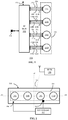
- FIG. 1 shows an antenna array 100 for determining location information for RF localisation or direction finding according to an embodiment.
- the antenna array 100 may include a number of antenna patches 110 for example as illustrated four antenna patches 110a, 110b, 110c, 110d. In other examples there may be fewer or more than four patches. If more than four patches are used, it may be easier for a localization or direction finding procedure to eliminate reflected signals. This is because methods for angle of arrival calculation may be sensitive to the number of received reflections. More antennas with specific spacing (given by the received wave length) can help to eliminate unwanted reflections. The only line of sight (direct free space path) signal is the ideal signal for localization. If two or three patches are used it may not be possible to account for reflected signals in the localization.
- Each of the four patches 110a-d includes four feed-points 114a-d, 116a-d, 118a-d and 122a-d.
- a feed-point may be considered to include the location of the patch at which a connection to the antenna patch is made either to feed the RF signal from other circuitry when an antenna is used for transmission or to tap off a received RF signal which is then supplied to further circuitry when the antenna is used to receive a signal.
- the feed-points may be coaxial feed-points having a signal path at least partially shielded by a ground.
- feed-points 114a-d, 116a-d, 118a-d and 122a-d are shown for each of the patches 110a-d, but in other examples there may be two or more feed-points. Adding feed-points may reduce the gain of each antenna patch compared to a patch with a single feed-point.
- the feed-points 114a-d, 116a-d, 118a-d and 122a-d may be connected to an RF multiplexer 102.
- the RF multiplexer 102 may include a number of switches typically implemented using MOSFETs or other transistors.
- the RF multiplexer 102 may have a control input connected to control input terminal 106.
- the RF multiplexer 102 may have a RF signal terminal connected to RF terminal 104.
- the control input may determine which of the feed-points 114a-d, 116a-d, 118a-d and 122a-d are connected to the RF terminal 104 via multiplexer signal terminal.
- the RF multiplexer 102 may be controlled via control input terminal 106 to selectively couple the feed-points 114a-d, 116a-d, 118a-d and 122a-d one at a time to the RF terminal 104.
- each of the different feed-points 114a-d, 116a-d, 118a-d and 122a-d when selected may affect the sensitivity of the patch 110a-d to a particular polarization plane of a received RF signal.
- the antenna-array 100 may be considered to be a multi-polarized antenna array. As illustrated the antenna array 100 implements a multi-polarized antenna array consisting of 16 antennas.
- the RF signals received by each of the antennas may be routed to a processor or controller (not shown) via the RF multiplexer 102 which may then determine location information such as angle of arrival from the received RF signals.
- a circular patch may allow a symmetrical response in all directions without having a dependency on the probe angle position of the patch.
- other symmetrical shapes such as squares, rectangles, star, or ellipses may be used. Some of these shapes may result in a different frequency response dependent on the location of the probe feed-point. Shapes with corners may have distortions and consequently in some examples shapes with rounded edges may be used.
- the antenna array 100 is a uniform linear antenna array which may allow the angle of arrival of a detected RF signal to be determined with minimal computation overhead.
- other examples may use different arrangements of antenna patches for example a matrix or a nonlinear arrangement of the antenna patches.
- Some examples may use a uniform circular array or uniform matrix array. The arrangement of the antenna patches may determine which localization algorithm is used.
- FIG. 2 shows an RF receiver including the antenna array 100 and a controller 112.
- the antenna patches 110 may be implemented on a substrate such as a multi-layer printed circuit board.
- the RF multiplexer 102 (not shown) may also be implemented by one or more RF switches.
- the controller 112 may have an RF input connected to the RF terminal 106 using a connecter such as for example a sub-miniature version A (SMA) RF connector.
- SMA sub-miniature version A
- the controller 112 as illustrated may be included on the same substrate as the antenna array 100 or a different printed circuit board.
- the controller 112 may be implemented in hardware or a combination of hardware and software for example software executed on microprocessor, microcontroller or digital signal processor.
- the controller 112 may be implemented as a single device or multiple devices.
- the controller may have a control output connected to the control input 106.
- the controller 112 may perform a localisation procedure to determine an approximate relative location of an RF transmitter 150 from a number of RF signals received from that transmitter. This localisation procedure may occur during a predetermined time period or localization time period. For example some applications used wireless standards such as Bluetooth may initiate a localization procedure during a start-up or initialization phase.
- the controller 112 may control the RF multiplexer 102 to select the feed-points 114a-d, 116a-d, 118a-d and 122a-d one at a time via control connections 106.
- the controller 112 may sequentially select each of the four feed-points 114a, 116a, 118a, 122a of patch 110a followed by each of the four feed-points 114b, 116b, 118b, 122b of patch 110ab then each of the feed-points 114c, 116c, 118c, 122c of patch 110c and finally each of the feed-points 114d, 116d, 118d, 122d of patch 110d.
- different selection sequences may be used.
- the RF receiver may be incorporated together with an RF transmitter circuit and the antenna array 100 may be used for receiving and transmitting RF signals.
- the RF multiplexer 102 may be implemented using MOS transistor switches or other transistor switches.
- the RF multiplexer 102 may be a single device or multiple devices.
- RF transmitter 150 may transmit a RF signal having an angle of arrival 108 which may vary from -90 degrees to +90 degrees.
- This RF signal may be detected by the active selected antenna corresponding to the selected patch, that is to say one of 110a-d and the selected feed-point in the selected patch.
- the RF signal transmitted by the transmitter is detected by the equivalent of 16 separate antennas.
- Each of the different feed-points correspond to an antenna which is sensitive to a particular polarization plane, although adding multiple feed-points may reduce the effective antenna gain.
- the RF signal detected by each of the different antennas may then be used by the controller 112 to determine location information such as an angle of arrival and/or RSSI using known methods and so determine a measure of the relative location of the RF receiver 100 to the RF transmitter 150.
- the antenna patches 110a-d may be uniformly distributed and be separated by a centre-to-centre distance equal to a fraction of the wavelength ( ⁇ ) of the RF signal of interest. For example the separation may be ⁇ /2, ⁇ /4 or ⁇ /8. The actual distance will depend on the geometry and the relative permittivity of the material used to make the substrate.
- the RF transmitter 150 may be included in a RF transceiver in a mobile device and the RF receiver including antenna array 100 may be included in a RF transceiver in a wireless router.
- this location information may be transmitted to the mobile device for use in various applications.
- Figures 3A, 3B, 3C , 3D, 3E show layers of the linear antenna array 100 according to one or more embodiments implemented on a multi-layer printed circuit board 120.
- FIG. 3A shows a plan view of the printed circuit board 120 showing the metal layer 120' used to form the antenna patches 110a-d.
- the metal has been removed from the dielectric region 146.
- the antenna patch 110a has a corresponding four coaxial feed-points 124a, 126a, 128a, and 130a.
- antenna patches 110b-d have corresponding four coaxial feed-points 124b-d, 126b-d, 128b-d, and 130b-d. These coaxial feed-points correspond to the location where a via contact is made to each of the antenna patches 110a-d.
- Figure 3B shows a plan view of the printed circuit board 120 showing a second metal layer 120" used to form the ground plane.
- the four coaxial feed-points 124a, 126a, 128a, and 130a include metal vias passing through the metal layer 120". Each metal via is separated by a dielectric region 144 from the metal region 148 which is typically a ground. Hence each via is shielded by a ground region similarly to a coaxial cable which may reduce signal interference.
- antenna patches 110b-d have corresponding four coaxial feed-points 124b-d, 126b-d, 128b-d, and 130b-d. These coaxial feed-points correspond to the location where a via contact is made to each of the antenna patches 110a-d.
- the dashed lines 110a'-d' show the position of the corresponding antenna patches 110a-d in the second metal layer 120"
- Figure 3C shows a plan view of the third metal layer 120"' used to form the co-planer waveguides 132a-d, 134a-d, 136a-d and 138a-d.
- Each of the antenna patches 1 10a-d has four corresponding waveguides.
- the co-planer waveguides 132a-d, 134a-d, 136a-d and 138a-d may be formed as a metal line for the signal with two parallel metal lines either side which may be ground lines. The signal and ground lines may be separated by cavities in the layer 120"'. As illustrated the co-planer waveguides 132a-d are routed in parallel.
- the waveguides 132a-d may diverge in direction as the orientation of the waveguides does not affect the sensitivity of the antenna to the polarization angle of the RF signal.
- the sensitivity of the antenna to the polarization angle is determined by the point of contact of the feed-point with the antenna patch 110a-d.
- the routing between the waveguides 132a-d and the multiplexers may be selected so that the total path from the antenna patches to each multiplexer input is the same. This may equalise the signal delay regardless of which antenna feed-point is selected which may simplify the subsequent processing of the RF signals.
- the antenna patch 110a may have a first co-planer waveguide 132a which is connected to the first coaxial feed-point 124a with a via (not shown), a second co-planer waveguide 134a which is coupled to the second coaxial feed-point 126a with a via (not shown), a third co-planer waveguide 136a which is coupled to the third coaxial feed-point 128a with a via (not shown), and a fourth co-planer waveguide 138a which is coupled to the fourth coaxial feed-point 130a with a via (not shown).
- co-planar waveguides 132b-d, 134b-d, 136b-d, and 138b-d are similarly coupled to corresponding coaxial feed-points 124b-d, 126b-d, 128b-d.
- Each of the co-planar wave guides may be coupled to a respective terminal of the RF multiplexer (not shown).
- the dashed lines 110a'-d' show the position of the corresponding antenna patches 110a-d in the metal layer 120' in relation to the respective waveguides.
- the dashed line A corresponds to horizontal or 0 degrees polarization.
- the antenna when fourth coaxial feed-point 130a is selected, the antenna is more sensitive to a horizontal polarized signal, when third coaxial feed-point 128a is selected, the antenna is more sensitive to a 45 degrees polarized signal, when second coaxial feed-point 126a is selected, the antenna is more sensitive to a 90 degrees or vertical polarized signal, when first coaxial feed-point 124a is selected, the antenna is more sensitive to a 135 degrees polarized signal. It will be appreciated that the polarization angles are relative to each other.
- Figure 3D shows a horizontal cross-section of printed circuit board 120 as indicated by dashed line A in figures 3A, 3B and 3C showing one of the antenna patches 110a.
- Cross section shows metal layers 120', 120",120'" alternating with dielectric layers 150,152,154.
- the first metal layer 120' is used to implement the antenna patch 110a.
- the second metal layer 120" implements a ground plane 140.
- the co-planar waveguide 138a is formed in the third metal later 120" and the wave guides are separated by a second metal layer 120" which may form a ground plane 140.
- Metal via 142 forms the coaxial feed-point 130a to the waveguide 138a.
- first metal layer 120' may have a thickness of 0.017 mm
- first dielectric layer 150 may have a thickness of 1.5 mm
- second metal layer 120" may have a thickness of 0.035 mm
- second dielectric layer 152 may have a thickness of 0.3 mm
- third metal layer 120'" may have a thickness of coplanar waveguides 0.017 mm.
- the dimensions of the layers may vary dependent on the material properties of the substrates used to implement the antenna array.
- Figure 3E shows a three-dimensional cross section of the printed circuit board 120 as indicated by dashed line A in figures 3A, 3B and 3C showing one of the antenna patches 110a omitting dielectric layer 154.
- Figure 3E shows more detail of one of the co-planar wave guides 138a which includes a signal line 138a_1, two ground lines 138a_2 either side of the signal line and two cavities 138a_3 between the signal line 138a_1 and the ground lines 138a_2.
- FIG. 4 shows an alternative implementation of an antenna array on a substrate 200 according to an embodiment.
- Four substantially circular metal antenna patches 210a-d may be equally separated by dielectric region 222.
- the feed-points 202a-d, 204a-d, 206a-d, 208a-d are formed by metal limbs 212 extending from the circular patches 210a-d.
- a respective input of the RF multiplexer (not shown) may be connected directly to the end of each of the feed-points 202a-d, 204a-d, 206a-d, 208a-d on the same layer of the printed circuit board.
- the feed-points 202a-d, 204a-d, 206a-d, 208a-d may further include vias (not shown) which connect the feed-points to co-planer waveguides or other waveguides.
- Figures 5 , 6 and 7 show measured parameters for an example antenna implemented as shown in figures 3A to 3E This antenna may receive signals having a frequency of approximately 2.4 GHz. Other example antenna may be tuned to a different frequency.
- Figure 5 shows a plot 250 of the reflection coefficient in dB on the y-axis varying between -50 and 0 versus the frequency on the x-axis varying between 2 GHz and 2.8 GHz.
- the response of the 16 different antenna corresponding to 4 feed-points multiplied by 4 antenna patches as shown in lines 252 is reasonably uniform.
- Figure 6 shows the antenna gain in dBi in three-dimensional space 260.
- the three-dimensional plot 262 corresponds to a gain between -5 and -35 dB indicated by the grey-scale 264.
- Figure 7 shows a polar char 270 showing the gain in the E-plane 272 and the H-plane 274 for one antenna. Table 1 below shows the corresponding values and frequency bandwidth.
- the frequency bandwidth 350 MHz so for example for an antenna tuned to a frequency of 2.4 GHz, signals in the range of 2.3 GHz and 2.5 GHz may also be detected.
- the antenna frequency bandwidth increases with additional feeding points, while the antenna gain decreases.
- the antenna array may use a modified FR4 dielectric material called 370HR for dielectric layers.
- the Antenna gain can be improved (up to 0 dBi) using a dedicated RF dielectric with lower dissipation factor , tan ⁇ , which represents losses in the dielectric material.
- tan ⁇ dissipation factor
- normal FR4 material has 10 times higher losses then the dedicated RF substrate. Lower losses may result in improved signal radiation from of the substrate material.
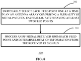
- Figure 8 shows a method of localization of an RF transmitter using a multi-polarized antenna 300.
- a probe feed-point may be switchably selected one at a time in an antenna array comprising a plurality of metal patches, each metal patch having at least two probe feed-points which may be coaxial feed-points.
- an RF signal received from each feed-point may be processed to determine location information of the RF signal which may be used for example to determine a location direction of an RF transmitter. Determining the location information may include determining an angle of arrival using any suitable method. Determining the location information may also include determination of the received signal strength indication (RSSI).
- RSSI received signal strength indication
- the multi-polarized antenna array includes a plurality of metal patches and a multiplexer. Each metal patch has at least two feed-points.
- the multiplexer is coupled to an RF terminal and to each of the at least two feed-points of each of the plurality of metal patches.
- the antenna array is configurable to couple each feed-point one at a time to the RF terminal. Location information may be determined by a controller coupled to the RF terminal from RF signals received via each feed-point.
- Examples of the RF receiver including the antenna array described herein may be included for example in a RF transceiver for example a Bluetooth LE or IEEE 802.15.4 for localization of a RF transmitter.
- the antenna array may arrange identical antenna elements along a line in space with uniform spacing.
- the Reflective power ratio S11 of the all antenna elements may be below -10 dB in the useful frequency band.
- the frequency bandwidth may be wider than 80 MHz if possible.
- the circular patches may result in a substantially isotropic radiation pattern. By having multiple feed-points for each antenna patch, the effective number of antenna is increased which may result in a reduced printed circuit board size for implementation.
- the set of instructions/method steps described above are implemented as functional and software instructions embodied as a set of executable instructions which are effected on a computer or machine which is programmed with and controlled by said executable instructions. Such instructions are loaded for execution on a processor (such as one or more CPUs).
- processor includes microprocessors, microcontrollers, processor modules or subsystems (including one or more microprocessors or microcontrollers), or other control or computing devices.
- a processor can refer to a single component or to plural components.
- the set of instructions/methods illustrated herein and data and instructions associated therewith are stored in respective storage devices, which are implemented as one or more non-transient machine or computer-readable or computer-usable storage media or mediums.
- Such computer-readable or computer usable storage medium or media is (are) considered to be part of an article (or article of manufacture).
- An article or article of manufacture can refer to any manufactured single component or multiple components.
- the non-transient machine or computer usable media or mediums as defined herein excludes signals, but such media or mediums may be capable of receiving and processing information from signals and/or other transient mediums.
- Example embodiments of the material discussed in this specification can be implemented in whole or in part through network, computer, or data based devices and/or services. These may include cloud, internet, intranet, mobile, desktop, processor, look-up table, microcontroller, consumer equipment, infrastructure, or other enabling devices and services. As may be used herein and in the claims, the following non-exclusive definitions are provided.
- one or more instructions or steps discussed herein are automated.
- the terms automated or automatically mean controlled operation of an apparatus, system, and/or process using computers and/or mechanical/electrical devices without the necessity of human intervention, observation, effort and/or decision.
Landscapes
- Engineering & Computer Science (AREA)
- Computer Networks & Wireless Communication (AREA)
- Signal Processing (AREA)
- Physics & Mathematics (AREA)
- General Physics & Mathematics (AREA)
- Radar, Positioning & Navigation (AREA)
- Remote Sensing (AREA)
- Waveguide Aerials (AREA)
- Variable-Direction Aerials And Aerial Arrays (AREA)
Abstract
Description
- This disclosure relates to a multi-polarized antenna array for localization and method for localization using a multi-polarized antenna array.
- Radio frequency (RF) transceivers for example Bluetooth, WiFi or other transceivers may use localization techniques for example using Angle of Arrival to estimate the relative location of a RF transmitter or transmitters from a received signal. This localization information may be used to support location based services for example to find an item or in indoor positioning systems to locate a point of interest. The RF transceiver may use an antenna array with predetermined phase difference between the antennas to receive multiple instances of the transmitted signal. These multiple received signals may then be used to determine the angle of arrival.
- Various aspects of the disclosure are defined in the accompanying claims.
- In a first aspect there is provided a multi-polarized antenna array for localization comprising: a plurality of metal patches, each metal patch having at least two feed-points; a multiplexer coupled to each of the at least two feed-points of each of the plurality of metal patches and having a signal terminal and a control terminal; wherein the antenna array is configurable to switchably couple each feed-point one at a time to the signal terminal, and to provide RF signals received via each feed-point to a controller configured to determine location information. In one or more embodiments each metal patch may be a symmetric shape.
- In one or more embodiments each metal patch may be substantially circular.
- In one or more embodiments each metal patch may be each metal patch may include four feed-points.
- In one or more embodiments for each metal patch: when the first feed-point of each metal patch is selected, the antenna array is configured to preferentially detect a signal having a first polarization; when the second feed-point is selected the antenna array is configured to preferentially detect a signal having a second polarization; when the third feed-point is selected the antenna array is configured to preferentially detect a signal having a third polarization; when the fourth feed-point is selected the antenna array is configured to preferentially detect a signal having a fourth polarization.
- In one or more embodiments the difference between the second polarization and the first polarization may be approximately 45 degrees, the difference between the third polarization and the second polarization may be approximately 45 degrees, and the difference between the fourth polarization may be the third polarization is approximately 45 degrees.
- In one or more embodiments, the antenna array may comprise a plurality of metal layers separated by dielectric layers, and wherein a first metal layer comprises the metal patches; a second metal layer comprises a ground plane; a third metal layer comprises a plurality of wave-guides; and wherein each feed-point of each metal patch is configured as a co-axial feed-point comprising a metal via between the first metal layer and the third metal layer and wherein each co-axial feed-point is coupled to a corresponding wave-guide and each wave-guide is coupled to the RF multiplexer..
- In one or more embodiments, each of the at least two feed-points of each of the plurality of metal patches may comprise a limb extending from the respective metal patch.
- In one or more embodiments, the antenna array may be configured as one of a linear antenna array, a circular antenna array, and a rectangular antenna array.
- In one or more embodiments, the plurality of metal patches may be identical and uniformly spaced.
- In one or more embodiments, the multi-polarized antenna array may be included in an RF receiver further comprising a controller coupled to a control input and the signal terminal of the multiplexer and configurable to control the multiplexer to switchably couple each feed-point one at a time to the signal terminal, and to determine location information from RF signals received via each feed-point.
- In one or more embodiments, the controller may be further configured to determine location information by determining the angle of arrival of the RF signals from the RF signals received at each feed-point.
- In a second aspect there is provided a method for localization using a multi-polarized antenna array comprising a plurality of metal patches, each metal patch having at least two feed-points, the method comprising switchably selecting each feed-point one at a time and determining location information from the RF signals detected via each feed-point.
- In one or more embodiments, the method may further comprise processing the RF signals received from each feed-point and determining an angle of arrival from the received RF signals.
- In one or more embodiments, the method may further comprise processing the RF signals received from each feed-point and determining a received signal strength indication from the received RF signals.
- In one or more embodiments, the method may further comprise detecting a first signal having a first polarization from one of the at least two feed-points and detecting a second signal having a second polarization from a second of the at least two feed-points.
- In a third aspect there is provided an apparatus for determining location information, the apparatus comprising: an antenna array comprising a plurality of metal patches, each metal patch having at least two feed-points; a multiplexer comprising a plurality of switches, each switch coupled to a respective feed-point; an RF terminal coupled to the plurality of switches; a controller coupled to a control input of the multiplexer and the RF terminal and configurable to switchably couple each feed-point one at a time to the RF terminal, and to determine location information from RF signals received via each feed-point.
- In one or more embodiments, the controller is configured during a predetermined time period to switchably couple each feed-point one at a time to the RF terminal. The predetermined time period may comprise a localization time period.
- In one or more embodiments, each of the at least two feed-points of each of the plurality of metal patches may comprise a limb extending from the respective metal patch.
- In one or more embodiments, each of the at least two feed-points of each of the plurality of metal patches may comprise a coaxial feed-point.
- In a fourth aspect there is described a computer program product comprising instructions which, when being executed by a processing unit included in a RF receiver comprising an antenna array, the antenna array comprising a plurality of metal patches, each metal patch having at least two feed-points, cause said processing unit to perform the steps of switchably selecting each feed-point one at a time and determining location information from the RF signals detected via each feed-point.
- In the figures and description like reference numerals refer to like features. Embodiments of are now described in detail, by way of example only, illustrated by the accompanying drawings in which:
-
Figure 1 shows a multi-polarized antenna array for determining location information. -
Figure 2 illustrates a RF receiver including the multi-polarized antenna array offigure 1 according to an example embodiment. -
Figures 3A, 3B, 3C ,3D, and 3E show different implementation layers of a linear antenna array according to one or more embodiments. -
Figure 3A shows a plan view of a first metal layer of an example embodiment of the linear antenna array including four antenna patches. -
Figure 3B shows a plan view of a second metal layer an example embodiment of the linear antenna array of including the ground plane. -
Figure 3C shows a plan view of a third metal layer of an example embodiment of the linear antenna array of including the coplanar waveguides. -
Figure 3D shows a cross section of part of the example embodiment of the linear antenna array shown infigure 3A, 3B, 3C . -
Figure 3E shows a three-dimensional cross section of part of the example embodiment of the linear antenna array shown infigure 3A, 3B, 3C ,3D . -
Figure 4 shows a plan view of an antenna array including the antenna patches according to an embodiment. -
Figure 5 shows a measured reflection coefficient of an example antenna array of the 16 antennas of the linear antenna array offigures 3A, 3B, 3C ,3D and 3E . -
Figure 6 shows a total gain plot of the linear antenna array offigures 3A, 3B, 3C ,3D and 3E . -
Figure 7 shows a polar plot of the E-plane and the H-plane of one antenna of the linear antenna array offigures 3A, 3B, 3C ,3D and 3E . -
Figure 8 shows a method of determining location information using a multi-polarized antenna array according to an example embodiment. -
Figure 1 shows anantenna array 100 for determining location information for RF localisation or direction finding according to an embodiment. Theantenna array 100 may include a number ofantenna patches 110 for example as illustrated fourantenna patches patches 110a-d includes four feed-points 114a-d, 116a-d, 118a-d and 122a-d. - In this disclosure a feed-point may be considered to include the location of the patch at which a connection to the antenna patch is made either to feed the RF signal from other circuitry when an antenna is used for transmission or to tap off a received RF signal which is then supplied to further circuitry when the antenna is used to receive a signal. In some examples the feed-points may be coaxial feed-points having a signal path at least partially shielded by a ground.
- As illustrated in
figure 1 , four feed-points 114a-d, 116a-d, 118a-d and 122a-d are shown for each of thepatches 110a-d, but in other examples there may be two or more feed-points. Adding feed-points may reduce the gain of each antenna patch compared to a patch with a single feed-point. The feed-points 114a-d, 116a-d, 118a-d and 122a-d may be connected to anRF multiplexer 102. TheRF multiplexer 102 may include a number of switches typically implemented using MOSFETs or other transistors. TheRF multiplexer 102 may have a control input connected tocontrol input terminal 106. TheRF multiplexer 102 may have a RF signal terminal connected toRF terminal 104. The control input may determine which of the feed-points 114a-d, 116a-d, 118a-d and 122a-d are connected to theRF terminal 104 via multiplexer signal terminal. In operation theRF multiplexer 102 may be controlled viacontrol input terminal 106 to selectively couple the feed-points 114a-d, 116a-d, 118a-d and 122a-d one at a time to theRF terminal 104. - Each of the different feed-
points 114a-d, 116a-d, 118a-d and 122a-d when selected may affect the sensitivity of thepatch 110a-d to a particular polarization plane of a received RF signal. Hence the antenna-array 100 may be considered to be a multi-polarized antenna array. As illustrated theantenna array 100 implements a multi-polarized antenna array consisting of 16 antennas. The RF signals received by each of the antennas may be routed to a processor or controller ( not shown) via theRF multiplexer 102 which may then determine location information such as angle of arrival from the received RF signals. - The inventors of the present disclosure have appreciated that adding multiple feed-points for each antenna patch which are then selected individually may allow a more compact antenna array to be formed since each antenna patch implements multiple antennas. A circular patch may allow a symmetrical response in all directions without having a dependency on the probe angle position of the patch. However, other symmetrical shapes such as squares, rectangles, star, or ellipses may be used. Some of these shapes may result in a different frequency response dependent on the location of the probe feed-point. Shapes with corners may have distortions and consequently in some examples shapes with rounded edges may be used.
- The
antenna array 100 is a uniform linear antenna array which may allow the angle of arrival of a detected RF signal to be determined with minimal computation overhead. However, other examples may use different arrangements of antenna patches for example a matrix or a nonlinear arrangement of the antenna patches. Some examples may use a uniform circular array or uniform matrix array. The arrangement of the antenna patches may determine which localization algorithm is used. -
Figure 2 shows an RF receiver including theantenna array 100 and acontroller 112. Theantenna patches 110 may be implemented on a substrate such as a multi-layer printed circuit board. The RF multiplexer 102 ( not shown) may also be implemented by one or more RF switches. Thecontroller 112 may have an RF input connected to theRF terminal 106 using a connecter such as for example a sub-miniature version A (SMA) RF connector. Thecontroller 112 as illustrated may be included on the same substrate as theantenna array 100 or a different printed circuit board. Thecontroller 112 may be implemented in hardware or a combination of hardware and software for example software executed on microprocessor, microcontroller or digital signal processor. Thecontroller 112 may be implemented as a single device or multiple devices. The controller may have a control output connected to thecontrol input 106. - In operation, the
controller 112 may perform a localisation procedure to determine an approximate relative location of anRF transmitter 150 from a number of RF signals received from that transmitter. This localisation procedure may occur during a predetermined time period or localization time period. For example some applications used wireless standards such as Bluetooth may initiate a localization procedure during a start-up or initialization phase. Thecontroller 112 may control theRF multiplexer 102 to select the feed-points 114a-d, 116a-d, 118a-d and 122a-d one at a time viacontrol connections 106. For example, thecontroller 112 may sequentially select each of the four feed-points patch 110a followed by each of the four feed-points points patch 110c and finally each of the feed-points patch 110d. In other examples, different selection sequences may be used. In some examples the RF receiver may be incorporated together with an RF transmitter circuit and theantenna array 100 may be used for receiving and transmitting RF signals. - The
RF multiplexer 102 may be implemented using MOS transistor switches or other transistor switches. TheRF multiplexer 102 may be a single device or multiple devices. -
RF transmitter 150 may transmit a RF signal having an angle ofarrival 108 which may vary from -90 degrees to +90 degrees. This RF signal may be detected by the active selected antenna corresponding to the selected patch, that is to say one of 110a-d and the selected feed-point in the selected patch. By cycling through all the feed-points the RF signal transmitted by the transmitter is detected by the equivalent of 16 separate antennas. Each of the different feed-points correspond to an antenna which is sensitive to a particular polarization plane, although adding multiple feed-points may reduce the effective antenna gain. - The RF signal detected by each of the different antennas may then be used by the
controller 112 to determine location information such as an angle of arrival and/or RSSI using known methods and so determine a measure of the relative location of theRF receiver 100 to theRF transmitter 150. Theantenna patches 110a-d may be uniformly distributed and be separated by a centre-to-centre distance equal to a fraction of the wavelength (λ) of the RF signal of interest. For example the separation may be λ/2, λ/4 or λ/8. The actual distance will depend on the geometry and the relative permittivity of the material used to make the substrate. - Having a separation between antenna patches corresponding to fractions of a wavelength may simplify some localization processes for example the determination of the angle-of-arrival. In some examples the
RF transmitter 150 may be included in a RF transceiver in a mobile device and the RF receiver includingantenna array 100 may be included in a RF transceiver in a wireless router. In this example, once the location information has been determined by the RF receiver, this location information may be transmitted to the mobile device for use in various applications. -
Figures 3A, 3B, 3C ,3D, 3E show layers of thelinear antenna array 100 according to one or more embodiments implemented on a multi-layer printedcircuit board 120. -
Figure 3A shows a plan view of the printedcircuit board 120 showing the metal layer 120' used to form theantenna patches 110a-d. The metal has been removed from thedielectric region 146. Theantenna patch 110a has a corresponding four coaxial feed-points antenna patches 110b-d have corresponding four coaxial feed-points 124b-d, 126b-d, 128b-d, and 130b-d. These coaxial feed-points correspond to the location where a via contact is made to each of theantenna patches 110a-d. -
Figure 3B shows a plan view of the printedcircuit board 120 showing asecond metal layer 120" used to form the ground plane. The four coaxial feed-points metal layer 120". Each metal via is separated by adielectric region 144 from themetal region 148 which is typically a ground. Hence each via is shielded by a ground region similarly to a coaxial cable which may reduce signal interference. Similarlyantenna patches 110b-d have corresponding four coaxial feed-points 124b-d, 126b-d, 128b-d, and 130b-d. These coaxial feed-points correspond to the location where a via contact is made to each of theantenna patches 110a-d.The dashedlines 110a'-d' show the position of the correspondingantenna patches 110a-d in thesecond metal layer 120" -
Figure 3C shows a plan view of thethird metal layer 120"' used to form the co-planer waveguides 132a-d, 134a-d, 136a-d and 138a-d. Each of theantenna patches 1 10a-d has four corresponding waveguides. The co-planer waveguides 132a-d, 134a-d, 136a-d and 138a-d may be formed as a metal line for the signal with two parallel metal lines either side which may be ground lines. The signal and ground lines may be separated by cavities in thelayer 120"'. As illustrated the co-planer waveguides 132a-d are routed in parallel. In other examples thewaveguides 132a-d may diverge in direction as the orientation of the waveguides does not affect the sensitivity of the antenna to the polarization angle of the RF signal. The sensitivity of the antenna to the polarization angle is determined by the point of contact of the feed-point with theantenna patch 110a-d. In some examples the routing between thewaveguides 132a-d and the multiplexers may be selected so that the total path from the antenna patches to each multiplexer input is the same. This may equalise the signal delay regardless of which antenna feed-point is selected which may simplify the subsequent processing of the RF signals. - For example the
antenna patch 110a may have a firstco-planer waveguide 132a which is connected to the first coaxial feed-point 124a with a via (not shown), a secondco-planer waveguide 134a which is coupled to the second coaxial feed-point 126a with a via (not shown), a thirdco-planer waveguide 136a which is coupled to the third coaxial feed-point 128a with a via (not shown), and a fourthco-planer waveguide 138a which is coupled to the fourth coaxial feed-point 130a with a via (not shown). The otherco-planar waveguides 132b-d, 134b-d, 136b-d, and 138b-d are similarly coupled to corresponding coaxial feed-points 124b-d, 126b-d, 128b-d. Each of the co-planar wave guides may be coupled to a respective terminal of the RF multiplexer (not shown). - The dashed
lines 110a'-d' show the position of the correspondingantenna patches 110a-d in the metal layer 120' in relation to the respective waveguides. The dashed line A corresponds to horizontal or 0 degrees polarization. With reference toantenna patch 110a, when fourth coaxial feed-point 130a is selected, the antenna is more sensitive to a horizontal polarized signal, when third coaxial feed-point 128a is selected, the antenna is more sensitive to a 45 degrees polarized signal, when second coaxial feed-point 126a is selected, the antenna is more sensitive to a 90 degrees or vertical polarized signal, when first coaxial feed-point 124a is selected, the antenna is more sensitive to a 135 degrees polarized signal. It will be appreciated that the polarization angles are relative to each other. -
Figure 3D shows a horizontal cross-section of printedcircuit board 120 as indicated by dashed line A infigures 3A, 3B and 3C showing one of theantenna patches 110a. Cross section showsmetal layers 120', 120",120'" alternating with dielectric layers 150,152,154. The first metal layer 120' is used to implement theantenna patch 110a. Thesecond metal layer 120" implements aground plane 140. Theco-planar waveguide 138a is formed in the third metal later 120" and the wave guides are separated by asecond metal layer 120" which may form aground plane 140. Metal via 142 forms the coaxial feed-point 130a to thewaveguide 138a. - As an example a first metal layer 120' may have a thickness of 0.017 mm, first
dielectric layer 150 may have a thickness of 1.5 mm,second metal layer 120" may have a thickness of 0.035 mm,second dielectric layer 152 may have a thickness of 0.3 mm, and third metal layer 120'" may have a thickness of coplanar waveguides 0.017 mm. The dimensions of the layers may vary dependent on the material properties of the substrates used to implement the antenna array. -
Figure 3E shows a three-dimensional cross section of the printedcircuit board 120 as indicated by dashed line A infigures 3A, 3B and 3C showing one of theantenna patches 110a omittingdielectric layer 154.Figure 3E shows more detail of one of the co-planar wave guides 138a which includes a signal line 138a_1, two ground lines 138a_2 either side of the signal line and two cavities 138a_3 between the signal line 138a_1 and the ground lines 138a_2. -
Figure 4 shows an alternative implementation of an antenna array on asubstrate 200 according to an embodiment. Four substantially circularmetal antenna patches 210a-d may be equally separated bydielectric region 222. In this example, the feed-points 202a-d, 204a-d, 206a-d, 208a-d are formed bymetal limbs 212 extending from thecircular patches 210a-d. In some examples a respective input of the RF multiplexer (not shown) may be connected directly to the end of each of the feed-points 202a-d, 204a-d, 206a-d, 208a-d on the same layer of the printed circuit board. In other examples the feed-points 202a-d, 204a-d, 206a-d, 208a-d may further include vias ( not shown) which connect the feed-points to co-planer waveguides or other waveguides. -
Figures 5 ,6 and 7 show measured parameters for an example antenna implemented as shown infigures 3A to 3E This antenna may receive signals having a frequency of approximately 2.4 GHz. Other example antenna may be tuned to a different frequency.Figure 5 shows aplot 250 of the reflection coefficient in dB on the y-axis varying between -50 and 0 versus the frequency on the x-axis varying between 2 GHz and 2.8 GHz. The response of the 16 different antenna corresponding to 4 feed-points multiplied by 4 antenna patches as shown inlines 252 is reasonably uniform. -
Figure 6 shows the antenna gain in dBi in three-dimensional space 260. The three-dimensional plot 262 corresponds to a gain between -5 and -35 dB indicated by the grey-scale 264.Figure 7 shows apolar char 270 showing the gain in theE-plane 272 and the H-plane 274 for one antenna. Table 1 below shows the corresponding values and frequency bandwidth.Table 1 Antenna/Feed-point Phi [°] Max_Gain [dBi] Theta radiation width [°] Freq bandwidth [MHz] Ant_01/124a 135 -5.67992 87 354.5 Ant_02/126a 90 -6.70911 84 354 Ant_03/128a 45 -6.84688 86 345 Ant_04/130a 0 -5.83957 83 333 Ant_05/124b 135 -5.82818 105 337.5 Ant_06/126b 90 -6.15797 83 347.5 Ant_07/128b 45 -6.96724 102 347 Ant_08/130b 0 -6.30252 86 331 Ant_09/124c 135 -6.3256 104 336 Ant_10/126c 90 -6.47986 86 348.5 Ant_11/128c 45 -7.28999 105 346.5 Ant_12/130c 0 -6.58646 133 338 Ant_13/124d 135 -5.67992 87 340.5 Ant_14/126d 90 -6.55092 83 347.5 Ant_15/128d 45 -6.3982 90 354.5 Ant_16/130d 0 -5.83957 81 341 - In this example, the frequency bandwidth 350 MHz so for example for an antenna tuned to a frequency of 2.4 GHz, signals in the range of 2.3 GHz and 2.5 GHz may also be detected. The worst case isolation among ports -5 dB in this example where there are 45° degrees between two adjacent ports. The lower total antenna gain -5.6 dBi. The antenna frequency bandwidth increases with additional feeding points, while the antenna gain decreases.
- In some examples the antenna array may use a modified FR4 dielectric material called 370HR for dielectric layers. In other examples, the Antenna gain can be improved (up to 0 dBi) using a dedicated RF dielectric with lower dissipation factor , tan δ, which represents losses in the dielectric material. For example normal FR4 material has 10 times higher losses then the dedicated RF substrate. Lower losses may result in improved signal radiation from of the substrate material.
-
Figure 8 shows a method of localization of an RF transmitter using amulti-polarized antenna 300. In step 302 a probe feed-point may be switchably selected one at a time in an antenna array comprising a plurality of metal patches, each metal patch having at least two probe feed-points which may be coaxial feed-points. Instep 304 an RF signal received from each feed-point may be processed to determine location information of the RF signal which may be used for example to determine a location direction of an RF transmitter. Determining the location information may include determining an angle of arrival using any suitable method. Determining the location information may also include determination of the received signal strength indication (RSSI). - An apparatus and method for determining location information using a multi-polarized antenna array is disclosed. The multi-polarized antenna array includes a plurality of metal patches and a multiplexer. Each metal patch has at least two feed-points. The multiplexer is coupled to an RF terminal and to each of the at least two feed-points of each of the plurality of metal patches. The antenna array is configurable to couple each feed-point one at a time to the RF terminal. Location information may be determined by a controller coupled to the RF terminal from RF signals received via each feed-point.
- Examples of the RF receiver including the antenna array described herein may be included for example in a RF transceiver for example a Bluetooth LE or IEEE 802.15.4 for localization of a RF transmitter. The antenna array may arrange identical antenna elements along a line in space with uniform spacing. In some example in the ISM band (2.4 GHz) the Reflective power ratio S11 of the all antenna elements may be below -10 dB in the useful frequency band. The frequency bandwidth may be wider than 80 MHz if possible. Further the circular patches may result in a substantially isotropic radiation pattern. By having multiple feed-points for each antenna patch, the effective number of antenna is increased which may result in a reduced printed circuit board size for implementation.
- In some example embodiments the set of instructions/method steps described above are implemented as functional and software instructions embodied as a set of executable instructions which are effected on a computer or machine which is programmed with and controlled by said executable instructions. Such instructions are loaded for execution on a processor (such as one or more CPUs). The term processor includes microprocessors, microcontrollers, processor modules or subsystems (including one or more microprocessors or microcontrollers), or other control or computing devices. A processor can refer to a single component or to plural components.
- In other examples, the set of instructions/methods illustrated herein and data and instructions associated therewith are stored in respective storage devices, which are implemented as one or more non-transient machine or computer-readable or computer-usable storage media or mediums. Such computer-readable or computer usable storage medium or media is (are) considered to be part of an article (or article of manufacture). An article or article of manufacture can refer to any manufactured single component or multiple components. The non-transient machine or computer usable media or mediums as defined herein excludes signals, but such media or mediums may be capable of receiving and processing information from signals and/or other transient mediums.
- Example embodiments of the material discussed in this specification can be implemented in whole or in part through network, computer, or data based devices and/or services. These may include cloud, internet, intranet, mobile, desktop, processor, look-up table, microcontroller, consumer equipment, infrastructure, or other enabling devices and services. As may be used herein and in the claims, the following non-exclusive definitions are provided.
- In one example, one or more instructions or steps discussed herein are automated. The terms automated or automatically (and like variations thereof) mean controlled operation of an apparatus, system, and/or process using computers and/or mechanical/electrical devices without the necessity of human intervention, observation, effort and/or decision.
- Although the appended claims are directed to particular combinations of features, it should be understood that the scope of the disclosure of the present invention also includes any novel feature or any novel combination of features disclosed herein either explicitly or implicitly or any generalisation thereof, whether or not it relates to the same invention as presently claimed in any claim and whether or not it mitigates any or all of the same technical problems as does the present invention.
- Features which are described in the context of separate embodiments may also be provided in combination in a single embodiment. Conversely, various features which are, for brevity, described in the context of a single embodiment, may also be provided separately or in any suitable sub combination.
- The applicant hereby gives notice that new claims may be formulated to such features and/or combinations of such features during the prosecution of the present application or of any further application derived therefrom.
- For the sake of completeness it is also stated that the term "comprising" does not exclude other elements or steps, the term "a" or "an" does not exclude a plurality, a single processor or other unit may fulfil the functions of several means recited in the claims and reference signs in the claims shall not be construed as limiting the scope of the claims.
Claims (15)
- A multi-polarized antenna array for localization comprising:a plurality of metal patches, each metal patch having at least two feed-points;a multiplexer coupled to each of the at least two feed-points of each of the plurality of metal patches and having a signal terminal and a control terminal;wherein the antenna array is configurable to switchably couple each feed-point one at a time to the signal terminal, and to provide RF signals received via each feedpoint to a controller configured to determine location information.
- The multi-polarized antenna array of claim 1 wherein each metal patch is a symmetric shape.
- The multi-polarized antenna array of any preceding claim wherein each metal patch is substantially circular.
- The multi-polarized antenna array of any preceding claim wherein each metal patch includes four feed-points.
- The multi-polarized antenna array of claim 4 wherein for each metal patch:when the first feed-point of each metal patch is selected, the antenna array is configured to preferentially detect a signal having a first polarization;when the second feed-point is selected the antenna array is configured to preferentially detect a signal having a second polarization;when the third feed-point is selected the antenna array is configured to preferentially detect a signal having a third polarization;when the fourth feed-point is selected the antenna array is configured to preferentially detect a signal having a fourth polarization.
- The multi-polarized antenna array of claim 5 wherein the difference between the second polarization and the first polarization is approximately 45 degrees, the difference between the third polarization and the second polarization is approximately 45 degrees, and the difference between the fourth polarization and the third polarization is approximately 45 degrees.
- The multi-polarized antenna array of any preceding claim comprising a plurality of metal layers separated by dielectric layers, and whereina first metal layer comprises the metal patches;a second metal layer comprises a ground plane;a third metal layer comprises a plurality of wave-guides; and wherein each feed-point of each metal patch is configured as a co-axial feed-point comprising a metal via between the first metal layer and the third metal layer and wherein each co-axial feed-point is coupled to a corresponding wave-guide and each wave-guide is coupled to the RF multiplexer.
- The multi-polarized antenna array of any preceding claim wherein each of the at least two feed-points of each of the plurality of metal patches comprises a limb extending from the respective metal patch.
- The multi-polarized antenna array of any preceding claim configured as one of a linear antenna array, a circular antenna array, and a rectangular antenna array.
- The multi-polarized antenna array of any preceding claim wherein the plurality of metal patches are identical and uniformly spaced.
- An RF receiver comprising the multi-polarized antenna array of any preceding claim and further comprising a controller coupled to a control input and the signal terminal of the multiplexer and configurable to control the multiplexer to switchably couple each feed-point one at a time to the signal terminal, and to determine location information from RF signals received via each feed-point.
- The RF receiver of any preceding claim wherein the controller is further configured to determine location information by determining the angle of arrival of the RF signals from the RF signals received at each feed-point.
- A method for localization using a multi-polarized antenna array comprising a plurality of metal patches, each metal patch having at least two feed-points, the method comprising switchably selecting each feed-point one at a time and determining location information from the RF signals detected via each feed-point.
- The method of claim 13 further comprising, processing the RF signals received from each feed-point and determining an angle of arrival from the received RF signals.
- The method of claim 13 or 14 further comprising, processing the RF signals received from each feed-point and determining a received signal strength indication from the received RF signals.
Priority Applications (3)
| Application Number | Priority Date | Filing Date | Title |
|---|---|---|---|
| EP19214617.3A EP3836301B1 (en) | 2019-12-09 | 2019-12-09 | Multi-polarized antenna array |
| US17/104,206 US11777228B2 (en) | 2019-12-09 | 2020-11-25 | Multi-polarized antenna array |
| CN202011431997.8A CN113036455B (en) | 2019-12-09 | 2020-12-09 | Multi-polarization antenna array |
Applications Claiming Priority (1)
| Application Number | Priority Date | Filing Date | Title |
|---|---|---|---|
| EP19214617.3A EP3836301B1 (en) | 2019-12-09 | 2019-12-09 | Multi-polarized antenna array |
Publications (2)
| Publication Number | Publication Date |
|---|---|
| EP3836301A1 true EP3836301A1 (en) | 2021-06-16 |
| EP3836301B1 EP3836301B1 (en) | 2024-01-24 |
Family
ID=68841013
Family Applications (1)
| Application Number | Title | Priority Date | Filing Date |
|---|---|---|---|
| EP19214617.3A Active EP3836301B1 (en) | 2019-12-09 | 2019-12-09 | Multi-polarized antenna array |
Country Status (3)
| Country | Link |
|---|---|
| US (1) | US11777228B2 (en) |
| EP (1) | EP3836301B1 (en) |
| CN (1) | CN113036455B (en) |
Families Citing this family (6)
| Publication number | Priority date | Publication date | Assignee | Title |
|---|---|---|---|---|
| US20230337941A1 (en) * | 2021-02-27 | 2023-10-26 | Stryker Corporation | System for determining patient support apparatus and medical device location |
| TWI776541B (en) * | 2021-06-07 | 2022-09-01 | 啓碁科技股份有限公司 | Antenna structure |
| FR3127077B1 (en) * | 2021-09-15 | 2024-08-23 | Commissariat Energie Atomique | Reconfigurable antenna network |
| TWI872686B (en) | 2023-09-06 | 2025-02-11 | 友達光電股份有限公司 | Liquid crystal antenna and method of beamforming |
| TWI892372B (en) * | 2023-12-21 | 2025-08-01 | 財團法人工業技術研究院 | Heterogeneous material integration antenna |
| CN119401110A (en) * | 2024-11-04 | 2025-02-07 | 北京理工大学长三角研究院(嘉兴) | A low-profile miniaturized broadband antenna and array |
Citations (5)
| Publication number | Priority date | Publication date | Assignee | Title |
|---|---|---|---|---|
| JP2014093599A (en) * | 2012-11-01 | 2014-05-19 | Mitsubishi Electric Corp | Array antenna device and method for controlling the same |
| WO2015068252A1 (en) * | 2013-11-08 | 2015-05-14 | 株式会社日立産機システム | Planar antenna, array antenna, and antenna system |
| GB2563834A (en) * | 2017-06-23 | 2019-01-02 | Decawave Ltd | Wideband antenna array |
| US20190273325A1 (en) * | 2018-03-02 | 2019-09-05 | Samsung Electro-Mechanics Co., Ltd. | Antenna apparatus |
| US20190372239A1 (en) * | 2017-02-01 | 2019-12-05 | Thales | Elementary antenna comprising a planar radiating device |
Family Cites Families (8)
| Publication number | Priority date | Publication date | Assignee | Title |
|---|---|---|---|---|
| JPS6326508A (en) * | 1986-07-19 | 1988-02-04 | Fujitsu Ltd | Inspection device for packaging component |
| JP2966690B2 (en) * | 1993-05-11 | 1999-10-25 | 松下電工株式会社 | Antenna device |
| US6992629B2 (en) * | 2003-09-03 | 2006-01-31 | Raytheon Company | Embedded RF vertical interconnect for flexible conformal antenna |
| US20100328142A1 (en) * | 2008-03-20 | 2010-12-30 | The Curators Of The University Of Missouri | Microwave and millimeter wave resonant sensor having perpendicular feed, and imaging system |
| US8633856B2 (en) | 2009-07-02 | 2014-01-21 | Blackberry Limited | Compact single feed dual-polarized dual-frequency band microstrip antenna array |
| GB2501507B (en) * | 2012-04-25 | 2014-09-24 | Toshiba Res Europ Ltd | Wireless communication methods and apparatus |
| US20130300602A1 (en) | 2012-05-08 | 2013-11-14 | Samsung Electronics Co., Ltd. | Antenna arrays with configurable polarizations and devices including such antenna arrays |
| CN108173002A (en) * | 2017-12-19 | 2018-06-15 | 哈尔滨工业大学(威海) | A Composite Polarization Sensitive Array Device Based on Conformal Vivaldi Antenna |
-
2019
- 2019-12-09 EP EP19214617.3A patent/EP3836301B1/en active Active
-
2020
- 2020-11-25 US US17/104,206 patent/US11777228B2/en active Active
- 2020-12-09 CN CN202011431997.8A patent/CN113036455B/en active Active
Patent Citations (5)
| Publication number | Priority date | Publication date | Assignee | Title |
|---|---|---|---|---|
| JP2014093599A (en) * | 2012-11-01 | 2014-05-19 | Mitsubishi Electric Corp | Array antenna device and method for controlling the same |
| WO2015068252A1 (en) * | 2013-11-08 | 2015-05-14 | 株式会社日立産機システム | Planar antenna, array antenna, and antenna system |
| US20190372239A1 (en) * | 2017-02-01 | 2019-12-05 | Thales | Elementary antenna comprising a planar radiating device |
| GB2563834A (en) * | 2017-06-23 | 2019-01-02 | Decawave Ltd | Wideband antenna array |
| US20190273325A1 (en) * | 2018-03-02 | 2019-09-05 | Samsung Electro-Mechanics Co., Ltd. | Antenna apparatus |
Also Published As
| Publication number | Publication date |
|---|---|
| EP3836301B1 (en) | 2024-01-24 |
| US20210175638A1 (en) | 2021-06-10 |
| US11777228B2 (en) | 2023-10-03 |
| CN113036455B (en) | 2025-09-26 |
| CN113036455A (en) | 2021-06-25 |
Similar Documents
| Publication | Publication Date | Title |
|---|---|---|
| EP3836301B1 (en) | Multi-polarized antenna array | |
| US11817638B2 (en) | Patch antenna | |
| US10283874B2 (en) | Antenna apparatus | |
| US9608313B2 (en) | On-chip waveguide feeder for millimeter wave ICS and feeding methods, and multiple input and output millimeter wave transceiver system using same | |
| US10854994B2 (en) | Broadband phased array antenna system with hybrid radiating elements | |
| US10651670B1 (en) | Electronic devices with wireless charging antenna arrays | |
| US8761699B2 (en) | Extendable-arm antennas, and modules and systems in which they are incorporated | |
| JP5596857B2 (en) | Antenna structure | |
| EP2045875A1 (en) | Antenna for radar device | |
| US20190267703A1 (en) | Antenna device for a radar detector having at least two radiation directions, and motor vehicle having at least one radar detector | |
| US11005185B2 (en) | Millimeter wave conformal slot antenna | |
| WO2007126600A2 (en) | Multiple antennas having good isolation disposed in a limited space | |
| EP3642906B1 (en) | Wideband antenna array | |
| WO2019073334A1 (en) | Antenna apparatus | |
| US8593368B2 (en) | Multi-band antenna and electronic apparatus having the same | |
| US12113300B2 (en) | Doppler motion sensor device with high isolation between antennas | |
| US20140347247A1 (en) | Antenna device for electronic device | |
| WO2023095643A1 (en) | Antenna module, and communication device equipped with same | |
| CN116724466B (en) | Dual band patch antenna for angle of arrival analysis | |
| CN117525832A (en) | An antenna, sensing module, sensor and electronic device | |
| KR20140101657A (en) | Ultra wideband dipole antenna | |
| US20100109962A1 (en) | Circularly polarized antenna and an electronic device having the circularly polarized antenna | |
| US20240372254A1 (en) | Calibrated antenna array | |
| US11909133B2 (en) | Dielectrically loaded printed dipole antenna | |
| JPH0846422A (en) | Microstrip antenna element for wireless communication and device equipped with the same |
Legal Events
| Date | Code | Title | Description |
|---|---|---|---|
| PUAI | Public reference made under article 153(3) epc to a published international application that has entered the european phase |
Free format text: ORIGINAL CODE: 0009012 |
|
| STAA | Information on the status of an ep patent application or granted ep patent |
Free format text: STATUS: THE APPLICATION HAS BEEN PUBLISHED |
|
| AK | Designated contracting states |
Kind code of ref document: A1 Designated state(s): AL AT BE BG CH CY CZ DE DK EE ES FI FR GB GR HR HU IE IS IT LI LT LU LV MC MK MT NL NO PL PT RO RS SE SI SK SM TR |
|
| STAA | Information on the status of an ep patent application or granted ep patent |
Free format text: STATUS: REQUEST FOR EXAMINATION WAS MADE |
|
| 17P | Request for examination filed |
Effective date: 20211216 |
|
| RBV | Designated contracting states (corrected) |
Designated state(s): AL AT BE BG CH CY CZ DE DK EE ES FI FR GB GR HR HU IE IS IT LI LT LU LV MC MK MT NL NO PL PT RO RS SE SI SK SM TR |
|
| GRAP | Despatch of communication of intention to grant a patent |
Free format text: ORIGINAL CODE: EPIDOSNIGR1 |
|
| STAA | Information on the status of an ep patent application or granted ep patent |
Free format text: STATUS: GRANT OF PATENT IS INTENDED |
|
| RIC1 | Information provided on ipc code assigned before grant |
Ipc: H01Q 21/06 20060101ALN20230815BHEP Ipc: H01Q 21/08 20060101ALN20230815BHEP Ipc: G01S 3/04 20060101ALI20230815BHEP Ipc: H01Q 21/24 20060101ALI20230815BHEP Ipc: H01Q 9/04 20060101ALI20230815BHEP Ipc: H01Q 1/12 20060101AFI20230815BHEP |
|
| INTG | Intention to grant announced |
Effective date: 20230901 |
|
| GRAS | Grant fee paid |
Free format text: ORIGINAL CODE: EPIDOSNIGR3 |
|
| GRAA | (expected) grant |
Free format text: ORIGINAL CODE: 0009210 |
|
| STAA | Information on the status of an ep patent application or granted ep patent |
Free format text: STATUS: THE PATENT HAS BEEN GRANTED |
|
| AK | Designated contracting states |
Kind code of ref document: B1 Designated state(s): AL AT BE BG CH CY CZ DE DK EE ES FI FR GB GR HR HU IE IS IT LI LT LU LV MC MK MT NL NO PL PT RO RS SE SI SK SM TR |
|
| REG | Reference to a national code |
Ref country code: GB Ref legal event code: FG4D |
|
| REG | Reference to a national code |
Ref country code: CH Ref legal event code: EP |
|
| REG | Reference to a national code |
Ref country code: DE Ref legal event code: R096 Ref document number: 602019045500 Country of ref document: DE |
|
| REG | Reference to a national code |
Ref country code: IE Ref legal event code: FG4D |
|
| REG | Reference to a national code |
Ref country code: LT Ref legal event code: MG9D |
|
| REG | Reference to a national code |
Ref country code: NL Ref legal event code: MP Effective date: 20240124 |
|
| PG25 | Lapsed in a contracting state [announced via postgrant information from national office to epo] |
Ref country code: NL Free format text: LAPSE BECAUSE OF FAILURE TO SUBMIT A TRANSLATION OF THE DESCRIPTION OR TO PAY THE FEE WITHIN THE PRESCRIBED TIME-LIMIT Effective date: 20240124 |
|
| PG25 | Lapsed in a contracting state [announced via postgrant information from national office to epo] |
Ref country code: NL Free format text: LAPSE BECAUSE OF FAILURE TO SUBMIT A TRANSLATION OF THE DESCRIPTION OR TO PAY THE FEE WITHIN THE PRESCRIBED TIME-LIMIT Effective date: 20240124 |
|
| PG25 | Lapsed in a contracting state [announced via postgrant information from national office to epo] |
Ref country code: IS Free format text: LAPSE BECAUSE OF FAILURE TO SUBMIT A TRANSLATION OF THE DESCRIPTION OR TO PAY THE FEE WITHIN THE PRESCRIBED TIME-LIMIT Effective date: 20240524 |
|
| PG25 | Lapsed in a contracting state [announced via postgrant information from national office to epo] |
Ref country code: LT Free format text: LAPSE BECAUSE OF FAILURE TO SUBMIT A TRANSLATION OF THE DESCRIPTION OR TO PAY THE FEE WITHIN THE PRESCRIBED TIME-LIMIT Effective date: 20240124 |
|
| PG25 | Lapsed in a contracting state [announced via postgrant information from national office to epo] |
Ref country code: GR Free format text: LAPSE BECAUSE OF FAILURE TO SUBMIT A TRANSLATION OF THE DESCRIPTION OR TO PAY THE FEE WITHIN THE PRESCRIBED TIME-LIMIT Effective date: 20240425 |
|
| REG | Reference to a national code |
Ref country code: AT Ref legal event code: MK05 Ref document number: 1652904 Country of ref document: AT Kind code of ref document: T Effective date: 20240124 |
|
| PG25 | Lapsed in a contracting state [announced via postgrant information from national office to epo] |
Ref country code: RS Free format text: LAPSE BECAUSE OF FAILURE TO SUBMIT A TRANSLATION OF THE DESCRIPTION OR TO PAY THE FEE WITHIN THE PRESCRIBED TIME-LIMIT Effective date: 20240424 Ref country code: HR Free format text: LAPSE BECAUSE OF FAILURE TO SUBMIT A TRANSLATION OF THE DESCRIPTION OR TO PAY THE FEE WITHIN THE PRESCRIBED TIME-LIMIT Effective date: 20240124 |
|
| PG25 | Lapsed in a contracting state [announced via postgrant information from national office to epo] |
Ref country code: ES Free format text: LAPSE BECAUSE OF FAILURE TO SUBMIT A TRANSLATION OF THE DESCRIPTION OR TO PAY THE FEE WITHIN THE PRESCRIBED TIME-LIMIT Effective date: 20240124 |
|
| PG25 | Lapsed in a contracting state [announced via postgrant information from national office to epo] |
Ref country code: AT Free format text: LAPSE BECAUSE OF FAILURE TO SUBMIT A TRANSLATION OF THE DESCRIPTION OR TO PAY THE FEE WITHIN THE PRESCRIBED TIME-LIMIT Effective date: 20240124 |
|
| PG25 | Lapsed in a contracting state [announced via postgrant information from national office to epo] |
Ref country code: RS Free format text: LAPSE BECAUSE OF FAILURE TO SUBMIT A TRANSLATION OF THE DESCRIPTION OR TO PAY THE FEE WITHIN THE PRESCRIBED TIME-LIMIT Effective date: 20240424 Ref country code: NO Free format text: LAPSE BECAUSE OF FAILURE TO SUBMIT A TRANSLATION OF THE DESCRIPTION OR TO PAY THE FEE WITHIN THE PRESCRIBED TIME-LIMIT Effective date: 20240424 Ref country code: LT Free format text: LAPSE BECAUSE OF FAILURE TO SUBMIT A TRANSLATION OF THE DESCRIPTION OR TO PAY THE FEE WITHIN THE PRESCRIBED TIME-LIMIT Effective date: 20240124 Ref country code: IS Free format text: LAPSE BECAUSE OF FAILURE TO SUBMIT A TRANSLATION OF THE DESCRIPTION OR TO PAY THE FEE WITHIN THE PRESCRIBED TIME-LIMIT Effective date: 20240524 Ref country code: HR Free format text: LAPSE BECAUSE OF FAILURE TO SUBMIT A TRANSLATION OF THE DESCRIPTION OR TO PAY THE FEE WITHIN THE PRESCRIBED TIME-LIMIT Effective date: 20240124 Ref country code: GR Free format text: LAPSE BECAUSE OF FAILURE TO SUBMIT A TRANSLATION OF THE DESCRIPTION OR TO PAY THE FEE WITHIN THE PRESCRIBED TIME-LIMIT Effective date: 20240425 Ref country code: FI Free format text: LAPSE BECAUSE OF FAILURE TO SUBMIT A TRANSLATION OF THE DESCRIPTION OR TO PAY THE FEE WITHIN THE PRESCRIBED TIME-LIMIT Effective date: 20240124 Ref country code: ES Free format text: LAPSE BECAUSE OF FAILURE TO SUBMIT A TRANSLATION OF THE DESCRIPTION OR TO PAY THE FEE WITHIN THE PRESCRIBED TIME-LIMIT Effective date: 20240124 Ref country code: BG Free format text: LAPSE BECAUSE OF FAILURE TO SUBMIT A TRANSLATION OF THE DESCRIPTION OR TO PAY THE FEE WITHIN THE PRESCRIBED TIME-LIMIT Effective date: 20240124 Ref country code: AT Free format text: LAPSE BECAUSE OF FAILURE TO SUBMIT A TRANSLATION OF THE DESCRIPTION OR TO PAY THE FEE WITHIN THE PRESCRIBED TIME-LIMIT Effective date: 20240124 |
|
| PG25 | Lapsed in a contracting state [announced via postgrant information from national office to epo] |
Ref country code: PL Free format text: LAPSE BECAUSE OF FAILURE TO SUBMIT A TRANSLATION OF THE DESCRIPTION OR TO PAY THE FEE WITHIN THE PRESCRIBED TIME-LIMIT Effective date: 20240124 Ref country code: PT Free format text: LAPSE BECAUSE OF FAILURE TO SUBMIT A TRANSLATION OF THE DESCRIPTION OR TO PAY THE FEE WITHIN THE PRESCRIBED TIME-LIMIT Effective date: 20240524 |
|
| PG25 | Lapsed in a contracting state [announced via postgrant information from national office to epo] |
Ref country code: SE Free format text: LAPSE BECAUSE OF FAILURE TO SUBMIT A TRANSLATION OF THE DESCRIPTION OR TO PAY THE FEE WITHIN THE PRESCRIBED TIME-LIMIT Effective date: 20240124 Ref country code: PT Free format text: LAPSE BECAUSE OF FAILURE TO SUBMIT A TRANSLATION OF THE DESCRIPTION OR TO PAY THE FEE WITHIN THE PRESCRIBED TIME-LIMIT Effective date: 20240524 Ref country code: PL Free format text: LAPSE BECAUSE OF FAILURE TO SUBMIT A TRANSLATION OF THE DESCRIPTION OR TO PAY THE FEE WITHIN THE PRESCRIBED TIME-LIMIT Effective date: 20240124 Ref country code: LV Free format text: LAPSE BECAUSE OF FAILURE TO SUBMIT A TRANSLATION OF THE DESCRIPTION OR TO PAY THE FEE WITHIN THE PRESCRIBED TIME-LIMIT Effective date: 20240124 |
|
| PG25 | Lapsed in a contracting state [announced via postgrant information from national office to epo] |
Ref country code: DK Free format text: LAPSE BECAUSE OF FAILURE TO SUBMIT A TRANSLATION OF THE DESCRIPTION OR TO PAY THE FEE WITHIN THE PRESCRIBED TIME-LIMIT Effective date: 20240124 |
|
| PG25 | Lapsed in a contracting state [announced via postgrant information from national office to epo] |
Ref country code: SM Free format text: LAPSE BECAUSE OF FAILURE TO SUBMIT A TRANSLATION OF THE DESCRIPTION OR TO PAY THE FEE WITHIN THE PRESCRIBED TIME-LIMIT Effective date: 20240124 |
|
| PG25 | Lapsed in a contracting state [announced via postgrant information from national office to epo] |
Ref country code: EE Free format text: LAPSE BECAUSE OF FAILURE TO SUBMIT A TRANSLATION OF THE DESCRIPTION OR TO PAY THE FEE WITHIN THE PRESCRIBED TIME-LIMIT Effective date: 20240124 Ref country code: CZ Free format text: LAPSE BECAUSE OF FAILURE TO SUBMIT A TRANSLATION OF THE DESCRIPTION OR TO PAY THE FEE WITHIN THE PRESCRIBED TIME-LIMIT Effective date: 20240124 |
|
| REG | Reference to a national code |
Ref country code: DE Ref legal event code: R097 Ref document number: 602019045500 Country of ref document: DE |
|
| PG25 | Lapsed in a contracting state [announced via postgrant information from national office to epo] |
Ref country code: SK Free format text: LAPSE BECAUSE OF FAILURE TO SUBMIT A TRANSLATION OF THE DESCRIPTION OR TO PAY THE FEE WITHIN THE PRESCRIBED TIME-LIMIT Effective date: 20240124 |
|
| PG25 | Lapsed in a contracting state [announced via postgrant information from national office to epo] |
Ref country code: SM Free format text: LAPSE BECAUSE OF FAILURE TO SUBMIT A TRANSLATION OF THE DESCRIPTION OR TO PAY THE FEE WITHIN THE PRESCRIBED TIME-LIMIT Effective date: 20240124 Ref country code: SK Free format text: LAPSE BECAUSE OF FAILURE TO SUBMIT A TRANSLATION OF THE DESCRIPTION OR TO PAY THE FEE WITHIN THE PRESCRIBED TIME-LIMIT Effective date: 20240124 Ref country code: RO Free format text: LAPSE BECAUSE OF FAILURE TO SUBMIT A TRANSLATION OF THE DESCRIPTION OR TO PAY THE FEE WITHIN THE PRESCRIBED TIME-LIMIT Effective date: 20240124 Ref country code: EE Free format text: LAPSE BECAUSE OF FAILURE TO SUBMIT A TRANSLATION OF THE DESCRIPTION OR TO PAY THE FEE WITHIN THE PRESCRIBED TIME-LIMIT Effective date: 20240124 Ref country code: DK Free format text: LAPSE BECAUSE OF FAILURE TO SUBMIT A TRANSLATION OF THE DESCRIPTION OR TO PAY THE FEE WITHIN THE PRESCRIBED TIME-LIMIT Effective date: 20240124 Ref country code: CZ Free format text: LAPSE BECAUSE OF FAILURE TO SUBMIT A TRANSLATION OF THE DESCRIPTION OR TO PAY THE FEE WITHIN THE PRESCRIBED TIME-LIMIT Effective date: 20240124 |
|
| PLBE | No opposition filed within time limit |
Free format text: ORIGINAL CODE: 0009261 |
|
| STAA | Information on the status of an ep patent application or granted ep patent |
Free format text: STATUS: NO OPPOSITION FILED WITHIN TIME LIMIT |
|
| PG25 | Lapsed in a contracting state [announced via postgrant information from national office to epo] |
Ref country code: IT Free format text: LAPSE BECAUSE OF FAILURE TO SUBMIT A TRANSLATION OF THE DESCRIPTION OR TO PAY THE FEE WITHIN THE PRESCRIBED TIME-LIMIT Effective date: 20240124 |
|
| PG25 | Lapsed in a contracting state [announced via postgrant information from national office to epo] |
Ref country code: IT Free format text: LAPSE BECAUSE OF FAILURE TO SUBMIT A TRANSLATION OF THE DESCRIPTION OR TO PAY THE FEE WITHIN THE PRESCRIBED TIME-LIMIT Effective date: 20240124 |
|
| 26N | No opposition filed |
Effective date: 20241025 |
|
| PG25 | Lapsed in a contracting state [announced via postgrant information from national office to epo] |
Ref country code: SI Free format text: LAPSE BECAUSE OF FAILURE TO SUBMIT A TRANSLATION OF THE DESCRIPTION OR TO PAY THE FEE WITHIN THE PRESCRIBED TIME-LIMIT Effective date: 20240124 |
|
| PG25 | Lapsed in a contracting state [announced via postgrant information from national office to epo] |
Ref country code: MC Free format text: LAPSE BECAUSE OF FAILURE TO SUBMIT A TRANSLATION OF THE DESCRIPTION OR TO PAY THE FEE WITHIN THE PRESCRIBED TIME-LIMIT Effective date: 20240124 |
|
| P01 | Opt-out of the competence of the unified patent court (upc) registered |
Free format text: CASE NUMBER: APP_29893/2025 Effective date: 20250623 |
|
| REG | Reference to a national code |
Ref country code: CH Ref legal event code: PL |
|
| PG25 | Lapsed in a contracting state [announced via postgrant information from national office to epo] |
Ref country code: LU Free format text: LAPSE BECAUSE OF NON-PAYMENT OF DUE FEES Effective date: 20241209 |
|
| GBPC | Gb: european patent ceased through non-payment of renewal fee |
Effective date: 20241209 |
|
| REG | Reference to a national code |
Ref country code: BE Ref legal event code: MM Effective date: 20241231 |
|
| PG25 | Lapsed in a contracting state [announced via postgrant information from national office to epo] |
Ref country code: GB Free format text: LAPSE BECAUSE OF NON-PAYMENT OF DUE FEES Effective date: 20241209 Ref country code: BE Free format text: LAPSE BECAUSE OF NON-PAYMENT OF DUE FEES Effective date: 20241231 |
|
| PG25 | Lapsed in a contracting state [announced via postgrant information from national office to epo] |
Ref country code: CH Free format text: LAPSE BECAUSE OF NON-PAYMENT OF DUE FEES Effective date: 20241231 |
|
| PG25 | Lapsed in a contracting state [announced via postgrant information from national office to epo] |
Ref country code: IE Free format text: LAPSE BECAUSE OF NON-PAYMENT OF DUE FEES Effective date: 20241209 |
|
| PGFP | Annual fee paid to national office [announced via postgrant information from national office to epo] |
Ref country code: DE Payment date: 20251126 Year of fee payment: 7 |
|
| PGFP | Annual fee paid to national office [announced via postgrant information from national office to epo] |
Ref country code: FR Payment date: 20251120 Year of fee payment: 7 |
|
| PG25 | Lapsed in a contracting state [announced via postgrant information from national office to epo] |
Ref country code: CY Free format text: LAPSE BECAUSE OF FAILURE TO SUBMIT A TRANSLATION OF THE DESCRIPTION OR TO PAY THE FEE WITHIN THE PRESCRIBED TIME-LIMIT Effective date: 20240124 |