EP3836198A1 - A method for forming a via hole self-aligned with a metal block on a substrate - Google Patents
A method for forming a via hole self-aligned with a metal block on a substrate Download PDFInfo
- Publication number
- EP3836198A1 EP3836198A1 EP19215615.6A EP19215615A EP3836198A1 EP 3836198 A1 EP3836198 A1 EP 3836198A1 EP 19215615 A EP19215615 A EP 19215615A EP 3836198 A1 EP3836198 A1 EP 3836198A1
- Authority
- EP
- European Patent Office
- Prior art keywords
- layer
- dielectric layer
- metal
- forming
- opening
- Prior art date
- Legal status (The legal status is an assumption and is not a legal conclusion. Google has not performed a legal analysis and makes no representation as to the accuracy of the status listed.)
- Granted
Links
Images









Classifications
-
- H—ELECTRICITY
- H10—SEMICONDUCTOR DEVICES; ELECTRIC SOLID-STATE DEVICES NOT OTHERWISE PROVIDED FOR
- H10W—GENERIC PACKAGES, INTERCONNECTIONS, CONNECTORS OR OTHER CONSTRUCTIONAL DETAILS OF DEVICES COVERED BY CLASS H10
- H10W20/00—Interconnections in chips, wafers or substrates
- H10W20/01—Manufacture or treatment
- H10W20/031—Manufacture or treatment of conductive parts of the interconnections
- H10W20/069—Manufacture or treatment of conductive parts of the interconnections by forming self-aligned vias or self-aligned contact plugs
-
- H—ELECTRICITY
- H10—SEMICONDUCTOR DEVICES; ELECTRIC SOLID-STATE DEVICES NOT OTHERWISE PROVIDED FOR
- H10W—GENERIC PACKAGES, INTERCONNECTIONS, CONNECTORS OR OTHER CONSTRUCTIONAL DETAILS OF DEVICES COVERED BY CLASS H10
- H10W20/00—Interconnections in chips, wafers or substrates
- H10W20/01—Manufacture or treatment
- H10W20/031—Manufacture or treatment of conductive parts of the interconnections
- H10W20/056—Manufacture or treatment of conductive parts of the interconnections by filling conductive material into holes, grooves or trenches
- H10W20/057—Manufacture or treatment of conductive parts of the interconnections by filling conductive material into holes, grooves or trenches by selectively depositing, e.g. by using selective CVD or plating
-
- H—ELECTRICITY
- H10—SEMICONDUCTOR DEVICES; ELECTRIC SOLID-STATE DEVICES NOT OTHERWISE PROVIDED FOR
- H10W—GENERIC PACKAGES, INTERCONNECTIONS, CONNECTORS OR OTHER CONSTRUCTIONAL DETAILS OF DEVICES COVERED BY CLASS H10
- H10W20/00—Interconnections in chips, wafers or substrates
- H10W20/01—Manufacture or treatment
- H10W20/031—Manufacture or treatment of conductive parts of the interconnections
- H10W20/069—Manufacture or treatment of conductive parts of the interconnections by forming self-aligned vias or self-aligned contact plugs
- H10W20/0693—Manufacture or treatment of conductive parts of the interconnections by forming self-aligned vias or self-aligned contact plugs by forming self-aligned vias
-
- H—ELECTRICITY
- H10—SEMICONDUCTOR DEVICES; ELECTRIC SOLID-STATE DEVICES NOT OTHERWISE PROVIDED FOR
- H10W—GENERIC PACKAGES, INTERCONNECTIONS, CONNECTORS OR OTHER CONSTRUCTIONAL DETAILS OF DEVICES COVERED BY CLASS H10
- H10W20/00—Interconnections in chips, wafers or substrates
- H10W20/01—Manufacture or treatment
- H10W20/071—Manufacture or treatment of dielectric parts thereof
- H10W20/074—Manufacture or treatment of dielectric parts thereof of dielectric parts comprising thin functional dielectric layers, e.g. dielectric etch-stop, barrier, capping or liner layers
- H10W20/077—Manufacture or treatment of dielectric parts thereof of dielectric parts comprising thin functional dielectric layers, e.g. dielectric etch-stop, barrier, capping or liner layers on sidewalls or on top surfaces of conductors
-
- H—ELECTRICITY
- H10—SEMICONDUCTOR DEVICES; ELECTRIC SOLID-STATE DEVICES NOT OTHERWISE PROVIDED FOR
- H10W—GENERIC PACKAGES, INTERCONNECTIONS, CONNECTORS OR OTHER CONSTRUCTIONAL DETAILS OF DEVICES COVERED BY CLASS H10
- H10W20/00—Interconnections in chips, wafers or substrates
- H10W20/01—Manufacture or treatment
- H10W20/071—Manufacture or treatment of dielectric parts thereof
- H10W20/081—Manufacture or treatment of dielectric parts thereof by forming openings in the dielectric parts
-
- H—ELECTRICITY
- H10—SEMICONDUCTOR DEVICES; ELECTRIC SOLID-STATE DEVICES NOT OTHERWISE PROVIDED FOR
- H10W—GENERIC PACKAGES, INTERCONNECTIONS, CONNECTORS OR OTHER CONSTRUCTIONAL DETAILS OF DEVICES COVERED BY CLASS H10
- H10W20/00—Interconnections in chips, wafers or substrates
- H10W20/01—Manufacture or treatment
- H10W20/071—Manufacture or treatment of dielectric parts thereof
- H10W20/081—Manufacture or treatment of dielectric parts thereof by forming openings in the dielectric parts
- H10W20/084—Manufacture or treatment of dielectric parts thereof by forming openings in the dielectric parts for dual-damascene structures
- H10W20/087—Manufacture or treatment of dielectric parts thereof by forming openings in the dielectric parts for dual-damascene structures involving multiple stacked pre-patterned masks
Definitions
- the present inventive concept relates to a method for forming a via hole self-aligned with a metal block on a substrate.
- An interconnection structure may include one or more interconnection levels or tiers, which are formed above the active device region.
- An interconnection level includes horizontal conductive paths or lines arranged in an insulating material layer. Conductive paths of different interconnection levels may be interconnected by conductive vias extending vertically through the insulating layers.
- an interconnection level is typically formed in what in the art is known as a "dual damascene process".
- horizontally extending trenches are etched in an insulating layer.
- vertically extending via holes are formed in the insulating layer.
- the trenches and via holes are simultaneously filled with a conductive material to form conductive lines in the trenches and conductive vias in the via holes.
- the process may be repeated to form a stack of interconnection levels.
- multiple patterning techniques like (litho etch)x, or pitch splitting techniques such as self-aligned double patterning (SADP) or quadruple patterning (SAQP), are typically employed during trench formation to enable conductive line patterns with sub-lithographic critical dimensions.
- SADP self-aligned double patterning
- SAQP quadruple patterning
- An objective of the present inventive concept is to provide an improved method allowing for improved self-alignment of a conductive line end with a vertically extending via hole.
- a further objective is to enable forming of conductive line ends and vertically extending via holes in a reliable and precise manner. Further and alternative objectives may be understood from the following.
- a method for forming a via hole self-aligned with a metal block on a substrate, the substrate comprising an interlayer dielectric layer comprising:
- the step of selective depositing of the metal block on the exposed second portion of the metal comprising layer allows depositing the metal block only on the exposed second portion of the metal comprising layer. Thereby, even if the opening in the second sacrificial layer exposes a portion of the dielectric layer adjacent to the exposed second portion of the metal comprising layer, the metal block selectively deposits on the exposed second portion of the metal comprising layer. In other words, the metal block will be formed on the exposed second portion of the metal comprising layer.
- the step of etching via the opening of the dielectric layer, through the remaining portion of the first portion of the metal comprising layer and the interlayer dielectric layer facilitate the via hole formation self-aligned with the metal block. This is since the metal block and also the dielectric layer act as mask and thereby the via hole becomes self-aligned with the metal block.
- the inventive method addresses the edge placement errors (EPE) by allowing a larger opening in the first sacrificial layer.
- EPE edge placement errors
- the allowance of a larger opening in the first sacrificial layer is due to the forming of the sidewall oxide layers on respective sidewalls of the parallel spacer line structures such that a portion of the dielectric layer is exposed between adjacent sidewall oxide layers i.e. forming what is commonly referred to as three different tones.
- a larger opening, less prone to alignment misplacement may consequently be formed in the first sacrificial layer while still being able to accurately align the metal block and the via hole.
- the inventive method allows forming the via hole self-aligned with the metal block.
- the self-aligning of the via hole with the metal block is due to the larger opening in the first sacrificial layer and also due to the forming of the opening in the second sacrificial layer partially overlapping the opening of the dielectric layer and exposing a second portion of the metal comprising layer.
- the advantage brought by forming the via hole self-aligned with the metal block is that the metal block defines a conductive line end.
- the inventive method allows accurately placing the via hole at a conductive line end.
- accurately placing the via hole at a conductive line end may simplify optical proximity correction (OPC) and hence facilitate fabrication of modern circuits.
- OPC optical proximity correction
- the inventive method allows for ever more aggressive line pitches e.g. by density improvement.
- inventive method does not need to allow for a line end extension for a via placement.
- inventive method is also compatible with the via hole and the metal block being separate or isolated. It should be noted that the inventive method may further proceed in a manner which per se is known in the art such as dual damascene process to transfer a pattern obtained by the inventive method into the interlayer dielectric layer.
- the opening in the second sacrificial layer may correspond to a portion of the opening in the first sacrificial layer.
- the opening in the second sacrificial layer may also be wider e.g. along the parallel spacer line structures with respect to the opening in the first sacrificial layer.
- the opening in the second sacrificial layer may also comprise a portion of the dielectric layer adjacent to the second portion of the metal comprising layer.
- the second portion of the metal comprising layer corresponding to a portion of the first portion of the metal comprising layer is hereby meant that the second portion of the metal comprising layer is a portion of the first portion of the metal comprising layer.
- exposing a remaining portion of the first portion of the metal comprising layer is hereby meant exposing a portion of the first portion of the metal comprising layer not covered by the metal block.
- the metal comprising layer may comprise any of or any combination of TiN, Ru, AlON, AlN, Pt, and TiO 2 .
- the metal comprising layer may be made of any of or any combination of TiN, Ru, AlON, AlN, Pt, and TiO 2 .
- the metal comprising layer may preferably be made of TiN.
- An advantage brought by TiN is that TiN may facilitate the step of etching as TiN may be etched in a controlled way e.g. to achieve smooth sharp features.
- Another advantage brought by TiN is that it may facilitate the step of forming the metal comprising layer since the stress in the TiN layer may be controlled. This may in turn result into an improved control on the roughness of the line edges obtained, subsequent to the transfer of the pattern obtained by the inventive method into the interlayer dielectric layer.
- the metal block may comprise any of or any combination of Ru, Rh, Pd, Os, Ir, and Pt.
- the metal block may be made of any of or any combination of the platinum group metals including Ru, Rh, Pd, Os, Ir, and Pt.
- the metal block may be made of a metal that may selectively be etched with respect to the metal comprising layer and the interlayer dielectric layer in the step of etching.
- the metal comprising layer is made of TiN
- the metal block may preferably be made of Ru, as TiN provides a good adhesion layer for Ru metal block.
- the metal comprising layer is made of TiN
- the metal block is made of Ru and the dielectric layer is made of SiN, the respective materials may selectively be etched with respect to each other.
- the selective deposition of the metal block may be performed by area selective deposition, ASD.
- ASD may allow selective deposition of the metal block only or primarily on the exposed second portion of the metal comprising layer.
- ASD of a metal will selectively deposit the metal in question on exposed metal comprising areas during the ASD process.
- ASD may further allow a robust selective deposition of the metal block e.g. providing an improved control on the selective deposition of the metal block.
- Some examples of the ASD are chemical vapor deposition (CVD), electroless electrochemistry deposition and atomic layer deposition (ALD).
- the selective deposition of the metal block may be performed by ALD.
- ALD may provide an even more improved control on the selective deposition of the metal block compared to the other ASD techniques.
- ALD may allow the metal block being deposited only on the exposed second portion of metal comprising layer in a more controlled manner e.g. with a controlled thickness.
- a lateral dimension of the opening defined in the first sacrificial layer in a direction along the parallel spacer line structures may be 1 to 2 times, preferably 1.5 times, a width of the via hole.
- a lateral dimension of the opening defined in the first sacrificial layer in a direction transvers to the parallel spacer line structures may be 1.5 to 5 times, preferably 2 times, a width of the via hole.
- the larger lateral dimensions of the opening in the first sacrificial layer i.e. along the parallel spacer line structures and transvers to the parallel spacer line structures may facilitate the alignment of the via hole with the metal block.
- the larger lateral dimensions of the opening in the first sacrificial layer may address EPE particularly for the ever more aggressive line pitches.
- the dielectric layer may comprise any of or any combination of SiN, SiO 2 , and SiCN.
- the dielectric material may be made of any of or any combination of SiN, SiO 2 , and SiCN.
- the dielectric layer may be any material which may be etched selective to the metal comprising layer, allowing exposing the first portion of the metal comprising layer.
- the parallel spacer line structures may comprise any of or any combination of amorphous silicon (a-Si), amorphous carbon (a-C) and SiO 2 .
- the parallel spacer line structures may be made of any of or any combination of a-Si, a-C and SiO 2 .
- the sidewall oxide layers may comprise any of or any combination of SiO 2 , SiN, or TiO x .
- the sidewall oxide layers may be made of any of or any combination of SiO 2 , SiN, or TiO x .
- Material of the parallel spacer line structures, the sidewall oxide layers and the dielectric layer may be selected based on etch selectivity. In other word, the material of each of the parallel spacer line structures, the sidewall oxide layers and the dielectric layer may be etched selective to the other two.
- the interlayer dielectric layer may comprise any of or any combination of SiO 2 , and SiCOH.
- the interlayer dielectric layer may be made of any of or any combination of SiO 2 , and SiCOH.
- the interlayer dielectric layer may be any dielectric material compatible with modern fabrication.
- Figs. 1-6 show a series of top and cross-sectional schematic views, demonstrating successive steps of an embodiment of the present inventive method.
- first, second, third and the like in the description and in the claims are used for distinguishing between similar elements and not necessarily for describing a sequence, either temporally, spatially, in ranking or in any other manner. It is to be understood that the terms so used are interchangeable under appropriate circumstances and that the embodiments of the invention described herein are capable of operation in other sequences than described or illustrated herein. Moreover, the terms top, bottom, over, under and the like in the description and the claims are used for descriptive purposes and not necessarily for describing relative positions. It is to be understood that the terms so used are interchangeable under appropriate circumstances and that the embodiments of the invention described herein are capable of operation in other orientations than described or illustrated herein.
- the present invention relates to a method for forming a via hole 200 self-aligned with a metal block 190.
- the metal block 190 and the via hole 200 are typically formed in the back-end of line (BEOL).
- BEOL back-end of line
- An embodiment of the method is shown in Figs. 1-6 .
- a cross-sectional schematic view of a structure 100 is shown.
- the structure 100 shown in Fig. 1 is provided on a substrate.
- the substrate comprises an interlayer dielectric layer 110.
- the structure 100 shown in Fig. 1 is provided by forming a metal comprising layer 120 on the interlayer dielectric layer 110, forming a dielectric layer 130 on the metal comprising layer 120, forming a plurality of parallel spacer line structures 140 on the dielectric layer 130, the parallel spacer line structures 140 extending along an upper surface of the dielectric layer 130.
- the structure 100 shown in Fig. 1 is further provided by forming a sidewall oxide layer 150 on respective sidewalls of the plurality of parallel spacer line structures 140 such that a portion of the dielectric layer 130 is exposed between adjacent sidewall oxide layers 150 of the parallel spacer line structures 140.
- the metal comprising layer 120, the dielectric layer 130, the parallel spacer line structures 140 and the sidewall oxide layer 150 may be formed using conventional methods known in the art. Those methods will not be described in detail to avoid undue lengthy discussions concerning methods per se already known to the skilled person.
- the axis Y denotes a vertical direction corresponding e.g. to a normal direction with respect to an upper surface of the dielectric layer 130.
- the axis X denotes a first horizontal direction along the upper surface of the dielectric layer 130 and the axis Z denotes a second horizontal direction along the upper surface of the dielectric layer 130, perpendicular to the first direction X.
- the substrate, the interlayer dielectric layer 110, the metal comprising layer 120, the dielectric layer 130, the parallel spacer line structures 140, and the sidewall oxide layer 150 will be described.
- the substrate may be any conventional substrate, suitable for semiconductor processing.
- the substrate may be a Si substrate, a Ge substrate, a SiGe substrate.
- Other examples include a silicon-on-insulator (SOI) substrate, a GeOI substrate or a SiGeOI substrate.
- the substrate comprises the interlayer dielectric layer 110.
- the interlayer dielectric layer 110 may be formed on an upper surface of the substrate.
- the interlayer dielectric layer 110 may comprise SiO 2 or SiCOH.
- the dielectric layer 110 may be formed in a manner which per se is known in the art such as chemical vapor deposition (CVD), plasma-enhanced CVD (PECVD) and spin coating.
- CVD chemical vapor deposition
- PECVD plasma-enhanced CVD
- spin coating A typical thickness of the interlayer dielectric layer 110 along Y axis may be in a range from 50 to 500nm.
- the metal comprising layer 120 may comprise any of or any combination of TiN, Ru, AION, AIN, Pt, and TiO 2 .
- the metal comprising layer may be formed in a manner which per se is known in the art such as CVD or physical vapor deposition (PVD).
- a typical thickness of the metal comprising layer 120 along Y axis may be in a range from 5 to 40nm.
- the dielectric layer 130 may be a dielectric layer such as a layer of silicon oxide or some other conventional low-k dielectric layer.
- the dielectric layer 130 may comprise SiN, SiO 2 , SiCN.
- the dielectric layer 130 may be formed in a manner which per se is known in the art such as CVD and PECVD. A typical thickness of the dielectric layer 130 along Y axis may be in a range from 5 to 30nm.
- the dielectric layer 130 may be any material which may be etched selective to the metal comprising layer 120.
- the dielectric layer 130 may be etched while the metal comprising layer may not be etched.
- the dielectric layer 130 may be etched significantly faster than the metal comprising layer 120 e.g. three times to twenty times faster, depending on etch chemistry and deposition technique.
- the plurality of parallel spacer line structures 140 may be formed in a manner which per se is known in the art.
- the plurality of parallel spacer line structures 140 may e.g. be formed by deposition of a layer followed by patterning of said layer. The patterning may be lithographically done. The patterning may define parallel line structures 140 with desired width.
- the plurality of parallel spacer line structures 140 may comprise any of or any combination of amorphous silicon, a-Si, amorphous carbon, a-C, or SiO 2 .
- a typical width of the plurality of parallel spacer line structures 140 along the X axis may be in a range from 5 to 40 nm.
- a typical thickness of the plurality of parallel spacer line structures 140 along the Y axis may be in a range from 20 to 100 nm.
- the sidewall oxide layers 150 may comprise any of or any combination of SiO 2 , SiN, or TiO x .
- the sidewall oxide layers 150 may be formed in a manner which per se is known in the art such as CVD or atomic layer deposition (ALD).
- the sidewall oxide layer 150 may e.g. be formed by depositing a conformal oxide layer of SiO 2 , SiN, or TiO x on the plurality of parallel spacer line structures 140.
- the conformal oxide layer may then be removed from upper surfaces of the parallel spacer line structures 140 and gaps in between the plurality of parallel spacer line structures 140 i.e. remained on side sidewalls of the plurality of parallel spacer line structures 140.
- a width of the sidewall oxide layers 150 on each respective side of the plurality of parallel spacer line structures 140 i.e. along the X axis may be in a range from 5 to 40 nm.
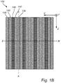
- Fig. 1a is a cross-sectional view of Fig. 1b along a line shown as BB' in Fig. 1b .
- Fig. 1c shows a cross-sectional vies of Fig. 1b along a line shown as AA' in Fig. 1b i.e. a cut through the dielectric layer 130.
- a stack of the interlayer dielectric layer 110, the metal comprising layer 120 and the dielectric layer 130 is shown.
- three different materials corresponding to the dielectric layer 130, the parallel spacer line structures 140 and the sidewall oxide layer 150 are visible from above, i.e. along the Y-axis. Those three different materials are commonly referred to as three different tones.
- the structure 100 has been processed further by forming a first sacrificial layer 160 covering exposed portions of the dielectric layer 130 and enclosing the parallel spacer line structures 140.
- the first sacrificial layer 160 may comprise a stack of layers.
- Fig. 2a shows a stack of two sacrificial layers 160 and 170.
- the first sacrificial layers 160 and 170 shown in Fig. 2a may comprise anti-reflective coatings such Spin-on Carbon (SOC) and Spin-on Glass (SOG) layers.
- SOC Spin-on Carbon
- SOG Spin-on Glass
- the first sacrificial layers 160 and 170 may be formed in a manner which per se is known in the art such as spin coating.
- a typical thickness of the first sacrificial layer 160 may be in a range of 20 to 100 nm.
- a typical thickness of the first sacrificial layer 170 may be in a range of 5 to 30 nm.
- Fig. 2a further shows how a mask layer 180 has been formed on the first sacrificial layers 160 and 170.
- the mask layer 180 shown in Fig. 2a has an opening corresponding to a first portion P of the dielectric layer 130 between adjacent sidewall oxide layers 150 of the parallel spacer line structures 140.
- the mask layer 180 may be formed in a manner which per se is known in the art.
- the opening in the mask layer 180 may be made in a manner which per se is known in the art.
- the opening in the mask layer 180 may be defined in a lithography step and the mask layer 180 may be a photoresist material.
- a lateral dimension of the opening, defined in the mask layer 180, along the X axis may be in a range of 5 to 40 nm.
- a lateral dimension of the opening, defined in the mask layer 180, along the Z axis may be in a range of 5 to 40 nm.
- Fig. 2a further shows that the structure 100 has been further processed by forming an opening O in the first sacrificial layer 160 to expose a first portion P of the dielectric layer 130 between adjacent sidewall oxide layers 150 of the parallel spacer line structures 140.
- the opening O in the first sacrificial layer 160 may be formed in a manner which per se is known in the art such as wet or dry etching of first sacrificial layer 160.
- the opening O in the first sacrificial layer 160 may be formed by halogen-based etching using e.g. C 4 F 6 or CF 4 . The etching may proceed to expose an upper surface of the first portion P of the dielectric layer 130.
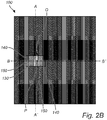
- Fig. 2b a simplified top view of the structure 100 shown in Fig. 2a is shown.
- Fig. 2b shows the dielectric layer 130, the parallel spacer line structures 140, and the sidewall oxide layers 150 under the mask layer 180 in relation to the opening O in the first sacrificial layer 160.
- Fig. 2a is a cross-sectional view of Fig. 2b along a line shown as BB' in Fig. 2b .
- Fig. 2c shows a cross sectional view of Fig. 2b along a line AA' shown in Fig. 2b .
- the structure 100 has been further processed by etching, via the opening O in the first sacrificial layer 160, through the first portion P of the dielectric layer 130, thereby forming an opening O' in the dielectric layer 130, exposing a first portion P' of the metal comprising layer 120.
- the etching through the first portion P of the dielectric layer 130 may be performed in a manner which per se is known in the art.
- the etching may e.g. be done using a plasma etch process with halogen chemistry such as CF 4 or C 4 F 6 .
- the etching through the first portion P of the dielectric layer 130 typically proceed to expose a first portion P' of the metal comprising layer 120.
- 3a further shows that the structure 100 has been further processed by removing the first sacrificial layers 160, 170, the mask layer 180.
- the removal of the first sacrificial layers 160 and 170 may be performed in a manner which per se is known in the art such as plasma etch.
- Fig. 3a shows a cross-sectional view of Fig. 3b along a line BB' shown in Fig. 3b .
- Fig. 3c shows a cross-sectional view of Fig. 3b along a line AA' shown in Fig. 3b .
- Fig. 3c shows the opening O' in the dielectric layer 130 which exposes the first portion P' of the metal comprising layer 120.
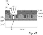
- the structure 100 has been provided by forming a second sacrificial layer 160 covering the dielectric layer 130, the first portion P' of the metal comprising layer 120 and enclosing the parallel spacer line structures 140.
- the second sacrificial layer 160 may comprise a stack of layers.
- Fig. 4a shows a stack of two sacrificial layers 160 and 170.
- the second sacrificial layers 160 and 170 may be formed in a similar manner as the first sacrificial layers 160 and 170.
- the second sacrificial layers 160 and 170 may be formed of the same materials of the first second sacrificial layers160 and 170.
- FIG. 4a further shows a mask layer 180 has been formed on the sacrificial layers 160 and 170.
- the mask layer 180 shown in Fig. 4a has an opening partially overlapping the opening O of the dielectric layer 130 and exposing a second portion P" of the metal comprising layer 120.
- the second portion P" of the metal comprising layer 120 corresponds to a portion of the first portion P' of the metal comprising layer 120.
- the mask layer 180 may be formed in a similar manner as the mask layer 180 formed on the first sacrificial layers 160 and 170.
- the opening in the mask layer 180 may be made in a manner which per se is known in the art. For instance, the opening in the mask layer 180 may be defined in a lithography step and the mask layer 180 may be a photoresist material.
- a lateral dimension of the opening, defined in the mask layer 180, along the X axis may be in a range of 20 to 40 nm.
- a lateral dimension of the opening, defined in the mask layer 180, along the Z axis may be in a range of 10 to 30 nm.
- Fig. 4a further shows that the structure 100 has been further processed by forming an opening O" in the second sacrificial layer 160, the opening O" partially overlapping the opening O of the dielectric layer 130 and exposing a second portion P" of the metal comprising layer 120.
- the second portion P" of the metal comprising layer 120 corresponds to a portion of the first portion P' of the metal comprising layer 120.
- the opening O" in the second sacrificial layer 160 may be performed in a manner in a similar manner as the opening of the first sacrificial layer 160.
- Fig. 4b shows the dielectric layer 130, the parallel spacer line structures 140, and the sidewall oxide layers 150 under the mask layer 180 in relation to the opening O" in the second sacrificial layer 160.
- Fig. 4a is a cross-sectional view of Fig. 4b along a line shown as BB' in Fig. 4b .
- Fig. 4c shows a cross sectional view of Fig. 4b along a line AA' shown in Fig. 4b .
- the structure 100 has been provided by selectively depositing a metal block 190 on the exposed second portion P" of the metal comprising layer 120.
- the selective deposition of the metal block 190 may be performed by area selective deposition (ASD).
- the ASD of the metal block 190 may be performed in a manner which per se is known in the art such as CVD, electroless electrochemistry deposition and ALD.
- the selective deposition of the metal block 190 may preferably be performed by atomic layer deposition (ALD).
- a typical thickness of the metal block 190 along the Y axis may be in a range of 1 to 10 nm.
- the thickness of the metal block 190 may be controlled by e.g. controlling a time of the ASD.
- the thickness of the metal block 190 may be controlled by e.g. controlling precursors flow during the ASD.
- the metal block may comprise any of or any combination of Ru, Rh, Pd, Os, Ir, and Pt.
- the metal block 190 and the metal comprising layer 120 may preferably be made of Ru and TiN respectively.
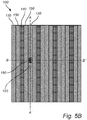
- Fig. 5b shows a top view of the structure 100 shown in Fig. 5a.
- Fig. 5a shows a cross-sectional view of Fig. 5b along a line BB' shown in Fig. 5b .
- Fig. 5c shows a cross-sectional view of the structure 100 shown in Fig 5b along a line AA' of Fig. 5b .
- Fig 5c shows that the metal block 190 has been selectively deposited on the exposed second portion P" of the metal comprising layer 120.
- the structure 100 has been provided by removing the second sacrificial layer 160, thereby exposing a remaining portion of the first portion P' of the metal comprising layer 120 in the opening O of the dielectric layer 130.
- the structure 100 has further been provided by etching, via the opening O' of the dielectric layer 130, through the remaining portion of the first portion P' of the metal comprising layer 120 and the interlayer dielectric layer 110, thereby forming a via hole 200 self-aligned with the metal block 190.
- the removing of the second sacrificial layer 160 may be performed in a manner as of the first sacrificial layer 160.
- etching via the opening O' of the dielectric layer 130, through the remaining portion of the first portion P' of the metal comprising layer 120 and the interlayer dielectric layer 110 may be performed in a manner which per se is known in the art such as wet or dry etching.
- An example of dry etching is reactive ion etching (RIE).
- RIE reactive ion etching
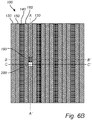
- Fig. 6b shows a top of the structure 100 wherein the via hole 200 self-aligned with the metal block 190 are shown.
- Fig. 6a shows a cross-sectional view of Fig. 6b along a line CC' shown in Fig. 6b . It should be noted that a cross-sectional view of Fig. 6b along a line BB' shown in Fig.
- Fig. 6b may look the same as Fig. 5a .
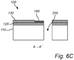
- Fig. 6c shows a cross-sectional view of Fig. 6b along a line AA' shown in Fig. 6b .
- Fig. 6c shows that the via hole 200 is self-aligned with the metal block 190.
- a lateral dimension of the via hole 200 along the X axis may be in a range from 5 to 30 nm.
- the lateral dimension of the via hole 200 along the X axis i.e. a width of the via hole 200 may be in the same range as a lateral dimension of the parallel spacer line structures 140 i.e. a width of the parallel spacer line structures 140 such as 5 to 25 nm.
- a lateral dimension of the via hole 200 along the Z axis may be in a range from 5 to 30 nm.
- a relation between the width of the via hole 200 and the opening O defined in the first sacrificial layer 160 may be as following: A lateral dimension of the opening O defined in the first sacrificial layer 160 in a direction along the parallel spacer line structures 140 i.e. along the Z axis may be 10 to 40 nm a width of the via hole 200.
- a lateral dimension of the opening O defined in the first sacrificial layer 160 in a direction transvers to the parallel spacer line structures 140 i.e. along the X axis may e.g. be times, preferably two times a width of the via hole 200.
- a lateral dimension of the metal block 190 along the X axis may be the same as the lateral dimension of the via hole 200 along the X axis.
- a lateral dimension of the metal block 190 along the Z axis may be in a range from 20 to 40 nm.
Landscapes
- Internal Circuitry In Semiconductor Integrated Circuit Devices (AREA)
Abstract
Description
- The present inventive concept relates to a method for forming a via hole self-aligned with a metal block on a substrate.
- Modern circuit fabrication typically includes processes of forming electrical interconnection structures for interconnecting semiconductor devices in a functioning circuit. An interconnection structure may include one or more interconnection levels or tiers, which are formed above the active device region. An interconnection level includes horizontal conductive paths or lines arranged in an insulating material layer. Conductive paths of different interconnection levels may be interconnected by conductive vias extending vertically through the insulating layers.
- In conventional circuit fabrication, an interconnection level is typically formed in what in the art is known as a "dual damascene process". According to this approach horizontally extending trenches are etched in an insulating layer. Further, vertically extending via holes are formed in the insulating layer. Thereafter the trenches and via holes are simultaneously filled with a conductive material to form conductive lines in the trenches and conductive vias in the via holes. The process may be repeated to form a stack of interconnection levels.
- In modern circuit fabrication, multiple patterning techniques like (litho etch)x, or pitch splitting techniques such as self-aligned double patterning (SADP) or quadruple patterning (SAQP), are typically employed during trench formation to enable conductive line patterns with sub-lithographic critical dimensions.
- However, using state-of-the-art patterning and block techniques it is becoming increasingly difficult to meet the desire for the ever more aggressive line pitches. In particular, it is becoming increasingly difficult to align conductive line ends with vertically extending via holes, due to edge placement errors (EPE) among others at such aggressive line pitches.
- An objective of the present inventive concept is to provide an improved method allowing for improved self-alignment of a conductive line end with a vertically extending via hole. A further objective is to enable forming of conductive line ends and vertically extending via holes in a reliable and precise manner. Further and alternative objectives may be understood from the following.
- According to an aspect of the present inventive concept there is
provided a method for forming a via hole self-aligned with a metal block on a substrate, the substrate comprising an interlayer dielectric layer, the method comprising: - forming a metal comprising layer on the interlayer dielectric layer,
- forming a dielectric layer on the metal comprising layer,
- forming a plurality of parallel spacer line structures on the dielectric layer, the parallel spacer line structures extending along an upper surface of the dielectric layer,
- forming a sidewall oxide layer on respective sidewalls of the plurality of parallel spacer line structures such that a portion of the dielectric layer is exposed between adjacent sidewall oxide layers of the parallel spacer line structures,
- forming a first sacrificial layer covering exposed portions of the dielectric layer and enclosing the parallel spacer line structures,
- forming an opening in the first sacrificial layer to expose a first portion of the dielectric layer between adjacent sidewall oxide layers of the parallel spacer line structures,
- etching, via the opening in the first sacrificial layer, through the first portion of the dielectric layer, thereby forming an opening in the dielectric layer, exposing a first portion of the metal comprising layer,
- removing the first sacrificial layer,
- forming a second sacrificial layer covering the dielectric layer, the first portion of the metal comprising layer and enclosing the parallel spacer line structures,
- forming an opening in the second sacrificial layer, the opening partially overlapping the opening of the dielectric layer and exposing a second portion of the metal comprising layer, the second portion of the metal comprising layer corresponding to a portion of the first portion of the metal comprising layer,
- selectively depositing a metal block on the exposed second portion of the metal comprising layer,
- removing the second sacrificial layer, thereby exposing a remaining portion of the first portion of the metal comprising layer in the opening of the dielectric layer,
- etching, via the opening of the dielectric layer, through the remaining portion of the first portion of the metal comprising layer and the interlayer dielectric layer, thereby forming a via hole self-aligned with the metal block.
- The step of selective depositing of the metal block on the exposed second portion of the metal comprising layer allows depositing the metal block only on the exposed second portion of the metal comprising layer. Thereby, even if the opening in the second sacrificial layer exposes a portion of the dielectric layer adjacent to the exposed second portion of the metal comprising layer, the metal block selectively deposits on the exposed second portion of the metal comprising layer. In other words, the metal block will be formed on the exposed second portion of the metal comprising layer.
- The step of etching via the opening of the dielectric layer, through the remaining portion of the first portion of the metal comprising layer and the interlayer dielectric layer facilitate the via hole formation self-aligned with the metal block. This is since the metal block and also the dielectric layer act as mask and thereby the via hole becomes self-aligned with the metal block.
- The inventive method addresses the edge placement errors (EPE) by allowing a larger opening in the first sacrificial layer. The allowance of a larger opening in the first sacrificial layer is due to the forming of the sidewall oxide layers on respective sidewalls of the parallel spacer line structures such that a portion of the dielectric layer is exposed between adjacent sidewall oxide layers i.e. forming what is commonly referred to as three different tones. Hence, a larger opening, less prone to alignment misplacement, may consequently be formed in the first sacrificial layer while still being able to accurately align the metal block and the via hole. In other words, the inventive method allows forming the via hole self-aligned with the metal block. The self-aligning of the via hole with the metal block is due to the larger opening in the first sacrificial layer and also due to the forming of the opening in the second sacrificial layer partially overlapping the opening of the dielectric layer and exposing a second portion of the metal comprising layer. The advantage brought by forming the via hole self-aligned with the metal block is that the metal block defines a conductive line end. Thereby, the inventive method allows accurately placing the via hole at a conductive line end. In addition, accurately placing the via hole at a conductive line end may simplify optical proximity correction (OPC) and hence facilitate fabrication of modern circuits. Furthermore, the inventive method allows for ever more aggressive line pitches e.g. by density improvement. Another advantage of the inventive method is that it does not need to allow for a line end extension for a via placement. The inventive method is also compatible with the via hole and the metal block being separate or isolated. It should be noted that the inventive method may further proceed in a manner which per se is known in the art such as dual damascene process to transfer a pattern obtained by the inventive method into the interlayer dielectric layer.
- By "forming an opening in the second sacrificial layer, the opening partially overlapping the opening of the dielectric layer" is hereby meant that the opening in the second sacrificial layer may correspond to a portion of the opening in the first sacrificial layer. The opening in the second sacrificial layer may also be wider e.g. along the parallel spacer line structures with respect to the opening in the first sacrificial layer. In other words, the opening in the second sacrificial layer may also comprise a portion of the dielectric layer adjacent to the second portion of the metal comprising layer.
- By "the second portion of the metal comprising layer corresponding to a portion of the first portion of the metal comprising layer" is hereby meant that the second portion of the metal comprising layer is a portion of the first portion of the metal comprising layer.
- By "exposing a remaining portion of the first portion of the metal comprising layer" is hereby meant exposing a portion of the first portion of the metal comprising layer not covered by the metal block.
- The metal comprising layer may comprise any of or any combination of TiN, Ru, AlON, AlN, Pt, and TiO2. The metal comprising layer may be made of any of or any combination of TiN, Ru, AlON, AlN, Pt, and TiO2. The metal comprising layer may preferably be made of TiN. An advantage brought by TiN is that TiN may facilitate the step of etching as TiN may be etched in a controlled way e.g. to achieve smooth sharp features. Another advantage brought by TiN is that it may facilitate the step of forming the metal comprising layer since the stress in the TiN layer may be controlled. This may in turn result into an improved control on the roughness of the line edges obtained, subsequent to the transfer of the pattern obtained by the inventive method into the interlayer dielectric layer.
- The metal block may comprise any of or any combination of Ru, Rh, Pd, Os, Ir, and Pt. The metal block may be made of any of or any combination of the platinum group metals including Ru, Rh, Pd, Os, Ir, and Pt. The metal block may be made of a metal that may selectively be etched with respect to the metal comprising layer and the interlayer dielectric layer in the step of etching. In the case that the metal comprising layer is made of TiN, the metal block may preferably be made of Ru, as TiN provides a good adhesion layer for Ru metal block. Moreover, if the metal comprising layer is made of TiN, the metal block is made of Ru and the dielectric layer is made of SiN, the respective materials may selectively be etched with respect to each other.
- The selective deposition of the metal block may be performed by area selective deposition, ASD. ASD may allow selective deposition of the metal block only or primarily on the exposed second portion of the metal comprising layer. As is known in the art, ASD of a metal will selectively deposit the metal in question on exposed metal comprising areas during the ASD process. ASD may further allow a robust selective deposition of the metal block e.g. providing an improved control on the selective deposition of the metal block. Some examples of the ASD are chemical vapor deposition (CVD), electroless electrochemistry deposition and atomic layer deposition (ALD).
- The selective deposition of the metal block may be performed by ALD. ALD may provide an even more improved control on the selective deposition of the metal block compared to the other ASD techniques. In other words, ALD may allow the metal block being deposited only on the exposed second portion of metal comprising layer in a more controlled manner e.g. with a controlled thickness.
- A lateral dimension of the opening defined in the first sacrificial layer in a direction along the parallel spacer line structures may be 1 to 2 times, preferably 1.5 times, a width of the via hole. A lateral dimension of the opening defined in the first sacrificial layer in a direction transvers to the parallel spacer line structures may be 1.5 to 5 times, preferably 2 times, a width of the via hole. The larger lateral dimensions of the opening in the first sacrificial layer i.e. along the parallel spacer line structures and transvers to the parallel spacer line structures may facilitate the alignment of the via hole with the metal block. In addition, the larger lateral dimensions of the opening in the first sacrificial layer may address EPE particularly for the ever more aggressive line pitches.
- The dielectric layer may comprise any of or any combination of SiN, SiO2, and SiCN. The dielectric material may be made of any of or any combination of SiN, SiO2, and SiCN. The dielectric layer may be any material which may be etched selective to the metal comprising layer, allowing exposing the first portion of the metal comprising layer.
- The parallel spacer line structures may comprise any of or any combination of amorphous silicon (a-Si), amorphous carbon (a-C) and SiO2. The parallel spacer line structures may be made of any of or any combination of a-Si, a-C and SiO2. The sidewall oxide layers may comprise any of or any combination of SiO2, SiN, or TiOx. The sidewall oxide layers may be made of any of or any combination of SiO2, SiN, or TiOx. Material of the parallel spacer line structures, the sidewall oxide layers and the dielectric layer may be selected based on etch selectivity. In other word, the material of each of the parallel spacer line structures, the sidewall oxide layers and the dielectric layer may be etched selective to the other two.
- The interlayer dielectric layer may comprise any of or any combination of SiO2, and SiCOH. The interlayer dielectric layer may be made of any of or any combination of SiO2, and SiCOH. The interlayer dielectric layer may be any dielectric material compatible with modern fabrication.
- The above and other characteristics, features and advantages of the present invention will become apparent from the following detailed description, taken in conjunction with the accompanying drawings, which illustrate, by way of example, the principles of the invention. This description is given for the sake of example only, without limiting the scope of the invention. The reference figures quoted below refer to the attached drawings.
-
Figs. 1-6 show a series of top and cross-sectional schematic views, demonstrating successive steps of an embodiment of the present inventive method. - In the different figures, the same reference signs refer to the same or analogous elements.
- The present invention will be described with respect to particular embodiments and with reference to certain drawings but the invention is not limited thereto but only by the claims. The drawings described are only schematic and are non-limiting. In the drawings, the size of some of the elements may be exaggerated and not drawn on scale for illustrative purposes. The dimensions and the relative dimensions do not correspond to actual reductions to practice of the invention.
- Furthermore, the terms first, second, third and the like in the description and in the claims, are used for distinguishing between similar elements and not necessarily for describing a sequence, either temporally, spatially, in ranking or in any other manner. It is to be understood that the terms so used are interchangeable under appropriate circumstances and that the embodiments of the invention described herein are capable of operation in other sequences than described or illustrated herein. Moreover, the terms top, bottom, over, under and the like in the description and the claims are used for descriptive purposes and not necessarily for describing relative positions. It is to be understood that the terms so used are interchangeable under appropriate circumstances and that the embodiments of the invention described herein are capable of operation in other orientations than described or illustrated herein.
- It is to be noticed that the term "comprising", used in the claims, should not be interpreted as being restricted to the means listed thereafter; it does not exclude other elements or steps. It is thus to be interpreted as specifying the presence of the stated features, integers, steps or components as referred to, but does not preclude the presence or addition of one or more other features, integers, steps or components, or groups thereof. Thus, the scope of the expression "a method comprising A and B" should not be limited to method consisting only of two steps A and B. It means that with respect to the present invention, the only relevant steps of the method are A and B.
- In the description provided herein, numerous specific details are set forth. However, it is understood that embodiments of the invention may be practiced without these specific details. In other instances, well-known methods, structures and techniques have not been shown in detail in order not to obscure an understanding of this description. The following terms are provided solely to aid in the understanding of the invention. The invention will now be described by a detailed description of several embodiments of the invention. It is clear that other embodiments of the invention can be configured according to the knowledge of persons skilled in the art without departing from the technical teaching of the invention, the invention being limited only by the terms of the appended claims.
- The present invention relates to a method for forming a via
hole 200 self-aligned with ametal block 190. Themetal block 190 and the viahole 200 are typically formed in the back-end of line (BEOL). An embodiment of the method is shown inFigs. 1-6 . - In connection with
Fig. 1a , a cross-sectional schematic view of astructure 100 is shown. Thestructure 100 shown inFig. 1 is provided on a substrate. The substrate comprises aninterlayer dielectric layer 110. Thestructure 100 shown inFig. 1 is provided by forming ametal comprising layer 120 on theinterlayer dielectric layer 110, forming adielectric layer 130 on themetal comprising layer 120, forming a plurality of parallelspacer line structures 140 on thedielectric layer 130, the parallelspacer line structures 140 extending along an upper surface of thedielectric layer 130. Thestructure 100 shown inFig. 1 is further provided by forming asidewall oxide layer 150 on respective sidewalls of the plurality of parallelspacer line structures 140 such that a portion of thedielectric layer 130 is exposed between adjacent sidewall oxide layers 150 of the parallelspacer line structures 140. - The
metal comprising layer 120, thedielectric layer 130, the parallelspacer line structures 140 and thesidewall oxide layer 150 may be formed using conventional methods known in the art. Those methods will not be described in detail to avoid undue lengthy discussions concerning methods per se already known to the skilled person. - In
Fig. 1 , the axis Y denotes a vertical direction corresponding e.g. to a normal direction with respect to an upper surface of thedielectric layer 130. The axis X denotes a first horizontal direction along the upper surface of thedielectric layer 130 and the axis Z denotes a second horizontal direction along the upper surface of thedielectric layer 130, perpendicular to the first direction X. In the following, the substrate, theinterlayer dielectric layer 110, themetal comprising layer 120, thedielectric layer 130, the parallelspacer line structures 140, and thesidewall oxide layer 150 will be described. - The substrate may be any conventional substrate, suitable for semiconductor processing. The substrate may be a Si substrate, a Ge substrate, a SiGe substrate. Other examples include a silicon-on-insulator (SOI) substrate, a GeOI substrate or a SiGeOI substrate. The substrate comprises the
interlayer dielectric layer 110. Theinterlayer dielectric layer 110 may be formed on an upper surface of the substrate. - The
interlayer dielectric layer 110 may comprise SiO2 or SiCOH. Thedielectric layer 110 may be formed in a manner which per se is known in the art such as chemical vapor deposition (CVD), plasma-enhanced CVD (PECVD) and spin coating. A typical thickness of theinterlayer dielectric layer 110 along Y axis may be in a range from 50 to 500nm. - The
metal comprising layer 120 may comprise any of or any combination of TiN, Ru, AION, AIN, Pt, and TiO2. The metal comprising layer may be formed in a manner which per se is known in the art such as CVD or physical vapor deposition (PVD). A typical thickness of themetal comprising layer 120 along Y axis may be in a range from 5 to 40nm. - The
dielectric layer 130 may be a dielectric layer such as a layer of silicon oxide or some other conventional low-k dielectric layer. Thedielectric layer 130 may comprise SiN, SiO2, SiCN. Thedielectric layer 130 may be formed in a manner which per se is known in the art such as CVD and PECVD. A typical thickness of thedielectric layer 130 along Y axis may be in a range from 5 to 30nm. Thedielectric layer 130 may be any material which may be etched selective to themetal comprising layer 120. Thedielectric layer 130 may be etched while the metal comprising layer may not be etched. Thedielectric layer 130 may be etched significantly faster than themetal comprising layer 120 e.g. three times to twenty times faster, depending on etch chemistry and deposition technique. - The plurality of parallel
spacer line structures 140 may be formed in a manner which per se is known in the art. The plurality of parallelspacer line structures 140 may e.g. be formed by deposition of a layer followed by patterning of said layer. The patterning may be lithographically done. The patterning may defineparallel line structures 140 with desired width. The plurality of parallelspacer line structures 140 may comprise any of or any combination of amorphous silicon, a-Si, amorphous carbon, a-C, or SiO2. A typical width of the plurality of parallelspacer line structures 140 along the X axis may be in a range from 5 to 40 nm. A typical thickness of the plurality of parallelspacer line structures 140 along the Y axis may be in a range from 20 to 100 nm. - The sidewall oxide layers 150 may comprise any of or any combination of SiO2, SiN, or TiOx. The sidewall oxide layers 150 may be formed in a manner which per se is known in the art such as CVD or atomic layer deposition (ALD). The
sidewall oxide layer 150 may e.g. be formed by depositing a conformal oxide layer of SiO2, SiN, or TiOx on the plurality of parallelspacer line structures 140. The conformal oxide layer may then be removed from upper surfaces of the parallelspacer line structures 140 and gaps in between the plurality of parallelspacer line structures 140 i.e. remained on side sidewalls of the plurality of parallelspacer line structures 140. A width of the sidewall oxide layers 150 on each respective side of the plurality of parallelspacer line structures 140 i.e. along the X axis may be in a range from 5 to 40 nm. - In connection with
Fig. 1b , a top view of thestructure 100 shown inFig. 1a is shown.Fig. 1a is a cross-sectional view ofFig. 1b along a line shown as BB' inFig. 1b .Fig. 1c shows a cross-sectional vies ofFig. 1b along a line shown as AA' inFig. 1b i.e. a cut through thedielectric layer 130. InFig. 1c , a stack of theinterlayer dielectric layer 110, themetal comprising layer 120 and thedielectric layer 130 is shown. As can be clearly seen inFig. 1b three different materials corresponding to thedielectric layer 130, the parallelspacer line structures 140 and thesidewall oxide layer 150 are visible from above, i.e. along the Y-axis. Those three different materials are commonly referred to as three different tones. - In connection with
Fig. 2a , thestructure 100 has been processed further by forming a firstsacrificial layer 160 covering exposed portions of thedielectric layer 130 and enclosing the parallelspacer line structures 140. The firstsacrificial layer 160 may comprise a stack of layers.Fig. 2a shows a stack of twosacrificial layers sacrificial layers Fig. 2a may comprise anti-reflective coatings such Spin-on Carbon (SOC) and Spin-on Glass (SOG) layers. The firstsacrificial layers sacrificial layer 160 may be in a range of 20 to 100 nm. A typical thickness of the firstsacrificial layer 170 may be in a range of 5 to 30 nm.Fig. 2a further shows how amask layer 180 has been formed on the firstsacrificial layers mask layer 180 shown inFig. 2a has an opening corresponding to a first portion P of thedielectric layer 130 between adjacent sidewall oxide layers 150 of the parallelspacer line structures 140. Themask layer 180 may be formed in a manner which per se is known in the art. The opening in themask layer 180 may be made in a manner which per se is known in the art. For instance, the opening in themask layer 180 may be defined in a lithography step and themask layer 180 may be a photoresist material. A lateral dimension of the opening, defined in themask layer 180, along the X axis may be in a range of 5 to 40 nm. A lateral dimension of the opening, defined in themask layer 180, along the Z axis may be in a range of 5 to 40 nm.Fig. 2a further shows that thestructure 100 has been further processed by forming an opening O in the firstsacrificial layer 160 to expose a first portion P of thedielectric layer 130 between adjacent sidewall oxide layers 150 of the parallelspacer line structures 140. The opening O in the firstsacrificial layer 160 may be formed in a manner which per se is known in the art such as wet or dry etching of firstsacrificial layer 160. For instance, the opening O in the firstsacrificial layer 160 may be formed by halogen-based etching using e.g. C4F6 or CF4. The etching may proceed to expose an upper surface of the first portion P of thedielectric layer 130. - In connection with
Fig. 2b , a simplified top view of thestructure 100 shown inFig. 2a is shown.Fig. 2b shows thedielectric layer 130, the parallelspacer line structures 140, and the sidewall oxide layers 150 under themask layer 180 in relation to the opening O in the firstsacrificial layer 160.Fig. 2a is a cross-sectional view ofFig. 2b along a line shown as BB' inFig. 2b .Fig. 2c shows a cross sectional view ofFig. 2b along a line AA' shown inFig. 2b . - In connection with
Fig. 3a , thestructure 100 has been further processed by etching, via the opening O in the firstsacrificial layer 160, through the first portion P of thedielectric layer 130, thereby forming an opening O' in thedielectric layer 130, exposing a first portion P' of themetal comprising layer 120. The etching through the first portion P of thedielectric layer 130 may be performed in a manner which per se is known in the art. The etching may e.g. be done using a plasma etch process with halogen chemistry such as CF4 or C4F6. The etching through the first portion P of thedielectric layer 130 typically proceed to expose a first portion P' of themetal comprising layer 120.Fig. 3a further shows that thestructure 100 has been further processed by removing the firstsacrificial layers mask layer 180. The removal of the firstsacrificial layers - In connection with
Fig. 3b a top view of thestructure 100 ofFig. 3a is shown.Fig. 3a shows a cross-sectional view ofFig. 3b along a line BB' shown inFig. 3b .Fig. 3c shows a cross-sectional view ofFig. 3b along a line AA' shown inFig. 3b .Fig. 3c shows the opening O' in thedielectric layer 130 which exposes the first portion P' of themetal comprising layer 120. - In connection with
Fig. 4a , thestructure 100 has been provided by forming a secondsacrificial layer 160 covering thedielectric layer 130, the first portion P' of themetal comprising layer 120 and enclosing the parallelspacer line structures 140. The secondsacrificial layer 160 may comprise a stack of layers.Fig. 4a shows a stack of twosacrificial layers sacrificial layers sacrificial layers sacrificial layers Fig. 4a further shows amask layer 180 has been formed on thesacrificial layers mask layer 180 shown inFig. 4a has an opening partially overlapping the opening O of thedielectric layer 130 and exposing a second portion P" of themetal comprising layer 120. The second portion P" of themetal comprising layer 120 corresponds to a portion of the first portion P' of themetal comprising layer 120. Themask layer 180 may be formed in a similar manner as themask layer 180 formed on the firstsacrificial layers mask layer 180 may be made in a manner which per se is known in the art. For instance, the opening in themask layer 180 may be defined in a lithography step and themask layer 180 may be a photoresist material. A lateral dimension of the opening, defined in themask layer 180, along the X axis may be in a range of 20 to 40 nm. A lateral dimension of the opening, defined in themask layer 180, along the Z axis may be in a range of 10 to 30 nm.Fig. 4a further shows that thestructure 100 has been further processed by forming an opening O" in the secondsacrificial layer 160, the opening O" partially overlapping the opening O of thedielectric layer 130 and exposing a second portion P" of themetal comprising layer 120. The second portion P" of themetal comprising layer 120 corresponds to a portion of the first portion P' of themetal comprising layer 120. The opening O" in the secondsacrificial layer 160 may be performed in a manner in a similar manner as the opening of the firstsacrificial layer 160. - In connection with 4b, a simplified top view of the
structure 100 shown inFig. 4a is shown.Fig. 4b shows thedielectric layer 130, the parallelspacer line structures 140, and the sidewall oxide layers 150 under themask layer 180 in relation to the opening O" in the secondsacrificial layer 160.Fig. 4a is a cross-sectional view ofFig. 4b along a line shown as BB' inFig. 4b .Fig. 4c shows a cross sectional view ofFig. 4b along a line AA' shown inFig. 4b . - In connection with
Fig. 5a , thestructure 100 has been provided by selectively depositing ametal block 190 on the exposed second portion P" of themetal comprising layer 120. The selective deposition of themetal block 190 may performed by area selective deposition (ASD). The ASD of themetal block 190 may be performed in a manner which per se is known in the art such as CVD, electroless electrochemistry deposition and ALD. The selective deposition of themetal block 190 may preferably be performed by atomic layer deposition (ALD). A typical thickness of themetal block 190 along the Y axis may be in a range of 1 to 10 nm. The thickness of themetal block 190 may be controlled by e.g. controlling a time of the ASD. The thickness of themetal block 190 may be controlled by e.g. controlling precursors flow during the ASD. The metal block may comprise any of or any combination of Ru, Rh, Pd, Os, Ir, and Pt. Themetal block 190 and themetal comprising layer 120 may preferably be made of Ru and TiN respectively.Fig. 5b shows a top view of thestructure 100 shown inFig. 5a. Fig. 5a shows a cross-sectional view ofFig. 5b along a line BB' shown inFig. 5b .Fig. 5c shows a cross-sectional view of thestructure 100 shown inFig 5b along a line AA' ofFig. 5b .Fig 5c shows that themetal block 190 has been selectively deposited on the exposed second portion P" of themetal comprising layer 120. - In connection with
Fig. 6a ,b andc , thestructure 100 has been provided by removing the secondsacrificial layer 160, thereby exposing a remaining portion of the first portion P' of themetal comprising layer 120 in the opening O of thedielectric layer 130. Thestructure 100 has further been provided by etching, via the opening O' of thedielectric layer 130, through the remaining portion of the first portion P' of themetal comprising layer 120 and theinterlayer dielectric layer 110, thereby forming a viahole 200 self-aligned with themetal block 190. The removing of the secondsacrificial layer 160 may be performed in a manner as of the firstsacrificial layer 160. The etching, via the opening O' of thedielectric layer 130, through the remaining portion of the first portion P' of themetal comprising layer 120 and theinterlayer dielectric layer 110 may be performed in a manner which per se is known in the art such as wet or dry etching. An example of dry etching is reactive ion etching (RIE).Fig. 6b shows a top of thestructure 100 wherein the viahole 200 self-aligned with themetal block 190 are shown.Fig. 6a shows a cross-sectional view ofFig. 6b along a line CC' shown inFig. 6b . It should be noted that a cross-sectional view ofFig. 6b along a line BB' shown inFig. 6b may look the same asFig. 5a .Fig. 6c shows a cross-sectional view ofFig. 6b along a line AA' shown inFig. 6b .Fig. 6c shows that the viahole 200 is self-aligned with themetal block 190. A lateral dimension of the viahole 200 along the X axis may be in a range from 5 to 30 nm. The lateral dimension of the viahole 200 along the X axis i.e. a width of the viahole 200 may be in the same range as a lateral dimension of the parallelspacer line structures 140 i.e. a width of the parallelspacer line structures 140 such as 5 to 25 nm. A lateral dimension of the viahole 200 along the Z axis may be in a range from 5 to 30 nm. A relation between the width of the viahole 200 and the opening O defined in the firstsacrificial layer 160 may be as following: A lateral dimension of the opening O defined in the firstsacrificial layer 160 in a direction along the parallelspacer line structures 140 i.e. along the Z axis may be 10 to 40 nm a width of the viahole 200. A lateral dimension of the opening O defined in the firstsacrificial layer 160 in a direction transvers to the parallelspacer line structures 140 i.e. along the X axis may e.g. be times, preferably two times a width of the viahole 200. A lateral dimension of themetal block 190 along the X axis may be the same as the lateral dimension of the viahole 200 along the X axis. A lateral dimension of themetal block 190 along the Z axis may be in a range from 20 to 40 nm. - In the above the inventive concept has mainly been described with reference to a limited number of examples. However, as is readily appreciated by a person skilled in the art, other examples than the ones disclosed above are equally possible within the scope of the inventive concept, as defined by the appended claims.
Claims (11)
- A method for forming a via hole (200) self-aligned with a metal block (190) on a substrate, the substrate comprising an interlayer dielectric layer (110), the method (300) comprising:forming a metal comprising layer (120) on the interlayer dielectric layer (110),forming a dielectric layer (130) on the metal comprising layer (120),forming a plurality of parallel spacer line structures (140) on the dielectric layer (130), the parallel spacer line structures (140) extending along an upper surface of the dielectric layer (130),forming a sidewall oxide layer (150) on respective sidewalls of the plurality of parallel spacer line structures (140) such that a portion of the dielectric layer (130) is exposed between adjacent sidewall oxide layers (150) of the parallel spacer line structures (140),forming a first sacrificial layer (160) covering exposed portions of the dielectric layer (130) and enclosing the parallel spacer line structures (140),forming an opening (O) in the first sacrificial layer (160) to expose a first portion (P) of the dielectric layer (130) between adjacent sidewall oxide layers (150) of the parallel spacer line structures (140),etching, via the opening (O) in the first sacrificial layer (160), through the first portion (P) of the dielectric layer (130), thereby forming an opening (O') in the dielectric layer (130), exposing a first portion (P') of the metal comprising layer (120),removing the first sacrificial layer (160),forming a second sacrificial layer (160) covering the dielectric layer (130), the first portion (P') of the metal comprising layer (120) and enclosing the parallel spacer line structures (140),forming an opening (O") in the second sacrificial layer (160), the opening (O") partially overlapping the opening (O') of the dielectric layer (130) and exposing a second portion (P") of the metal comprising layer (120), the second portion (P") of the metal comprising layer (120) corresponding to a portion of the first portion (P') of the metal comprising layer (120),selectively depositing a metal block (190) on the exposed second portion (P") of the metal comprising layer (120),removing the second sacrificial layer (160), thereby exposing a remaining portion of the first portion (P') of the metal comprising layer (120) in the opening of the dielectric layer (130), andetching, via the opening (P) of the dielectric layer (130), through the remaining portion of the first portion (P') of the metal comprising layer (120) and the interlayer dielectric layer (110), thereby forming a via hole (200) self-aligned with the metal block (190).
- The method according to claim 1, wherein the metal comprising layer (120) comprises any of or any combination of TiN, Ru, AION, AIN, Pt, and TiO2.
- The method according to claim 1 or 2, wherein the metal block (190) comprises any of or any combination of Ru, Rh, Pd, Os, Ir, and Pt.
- The method according to any one of claims 1-3, wherein the selective deposition of the metal block (190) is performed by area selective deposition, ASD.
- The method according to claim 4, wherein the selective deposition of the metal block (190) is performed by atomic layer deposition, ALD.
- The method according to any one of claims 1-5, wherein a lateral dimension of the opening (O) defined in the first sacrificial layer (160) in a direction along the parallel spacer line structures (140) is 1 to 2 times, preferably 1.5 times, a width of the via hole (200).
- The method according to any one of claims 1-6, wherein a lateral dimension of the opening (O) defined in the first sacrificial layer (160) in a direction transvers to the parallel spacer line structures (140) is 1.5 to 5 times, preferably 2 times, a width of the via hole (200).
- The method according to any one of claims 1-7, wherein the dielectric layer (130) comprises any of or any combination of SiN, SiO2, and SiCN.
- The method according to any one of claims 1-8, wherein the parallel spacer line structures (140) comprises any of or any combination of amorphous silicon, a-Si, amorphous carbon, a-C, and SiO2.
- The method according to any one of claims 1-9, wherein the sidewall oxide layers (150) comprises any of or any combination of SiO2, SiN, and TiOx.
- The method according to any one of claims 1-10, wherein the interlayer dielectric layer (110) comprises any of or any combination of SiO2 and SiCOH.
Priority Applications (2)
| Application Number | Priority Date | Filing Date | Title |
|---|---|---|---|
| EP19215615.6A EP3836198B1 (en) | 2019-12-12 | 2019-12-12 | A method for forming a via hole self-aligned with a metal block on a substrate |
| US17/110,631 US11270912B2 (en) | 2019-12-12 | 2020-12-03 | Method for forming a via hole self-aligned with a metal block on a substrate |
Applications Claiming Priority (1)
| Application Number | Priority Date | Filing Date | Title |
|---|---|---|---|
| EP19215615.6A EP3836198B1 (en) | 2019-12-12 | 2019-12-12 | A method for forming a via hole self-aligned with a metal block on a substrate |
Publications (2)
| Publication Number | Publication Date |
|---|---|
| EP3836198A1 true EP3836198A1 (en) | 2021-06-16 |
| EP3836198B1 EP3836198B1 (en) | 2022-08-24 |
Family
ID=68887320
Family Applications (1)
| Application Number | Title | Priority Date | Filing Date |
|---|---|---|---|
| EP19215615.6A Active EP3836198B1 (en) | 2019-12-12 | 2019-12-12 | A method for forming a via hole self-aligned with a metal block on a substrate |
Country Status (2)
| Country | Link |
|---|---|
| US (1) | US11270912B2 (en) |
| EP (1) | EP3836198B1 (en) |
Citations (3)
| Publication number | Priority date | Publication date | Assignee | Title |
|---|---|---|---|---|
| WO2015047321A1 (en) * | 2013-09-27 | 2015-04-02 | Intel Corporation | Previous layer self-aligned via and plug patterning for back end of line (beol) interconnects |
| US20170352591A1 (en) * | 2016-06-07 | 2017-12-07 | Globalfoundries Inc. | Method for producing self-aligned line end vias and related device |
| US20180261497A1 (en) * | 2017-02-10 | 2018-09-13 | Imec Vzw | Methods for forming conductive paths and vias |
Family Cites Families (8)
| Publication number | Priority date | Publication date | Assignee | Title |
|---|---|---|---|---|
| CN108780777B (en) | 2016-02-02 | 2023-02-17 | 东京毅力科创株式会社 | Self-aligning metal and vias using selective deposition |
| US10354912B2 (en) | 2016-03-21 | 2019-07-16 | Qualcomm Incorporated | Forming self-aligned vertical interconnect accesses (VIAs) in interconnect structures for integrated circuits (ICs) |
| US9607893B1 (en) | 2016-07-06 | 2017-03-28 | Globalfoundries Inc. | Method of forming self-aligned metal lines and vias |
| US10424507B2 (en) | 2017-04-04 | 2019-09-24 | Mirocmaterials LLC | Fully self-aligned via |
| US10249496B2 (en) * | 2017-05-05 | 2019-04-02 | Globalfoundries Inc. | Narrowed feature formation during a double patterning process |
| US10522394B2 (en) | 2017-09-25 | 2019-12-31 | Marvell World Trade Ltd. | Method of creating aligned vias in ultra-high density integrated circuits |
| US10269698B1 (en) | 2017-12-20 | 2019-04-23 | International Business Machines Corporation | Binary metallization structure for nanoscale dual damascene interconnects |
| US10395986B1 (en) | 2018-05-30 | 2019-08-27 | International Business Machines Corporation | Fully aligned via employing selective metal deposition |
-
2019
- 2019-12-12 EP EP19215615.6A patent/EP3836198B1/en active Active
-
2020
- 2020-12-03 US US17/110,631 patent/US11270912B2/en active Active
Patent Citations (3)
| Publication number | Priority date | Publication date | Assignee | Title |
|---|---|---|---|---|
| WO2015047321A1 (en) * | 2013-09-27 | 2015-04-02 | Intel Corporation | Previous layer self-aligned via and plug patterning for back end of line (beol) interconnects |
| US20170352591A1 (en) * | 2016-06-07 | 2017-12-07 | Globalfoundries Inc. | Method for producing self-aligned line end vias and related device |
| US20180261497A1 (en) * | 2017-02-10 | 2018-09-13 | Imec Vzw | Methods for forming conductive paths and vias |
Also Published As
| Publication number | Publication date |
|---|---|
| EP3836198B1 (en) | 2022-08-24 |
| US20210183698A1 (en) | 2021-06-17 |
| US11270912B2 (en) | 2022-03-08 |
Similar Documents
| Publication | Publication Date | Title |
|---|---|---|
| US11114439B2 (en) | Multi-division 3D NAND memory device | |
| TWI658537B (en) | Non-mandrel cutting | |
| EP3035379A1 (en) | Method for blocking a trench portion | |
| US9905424B1 (en) | Self-aligned non-mandrel cut formation for tone inversion | |
| KR20130115878A (en) | Method of manufacturing a contact structure | |
| KR20190087843A (en) | Semiconductor device | |
| US11127627B2 (en) | Method for forming an interconnection structure | |
| US9570397B1 (en) | Local interconnect structure including non-eroded contact via trenches | |
| US20180261497A1 (en) | Methods for forming conductive paths and vias | |
| CN108735661B (en) | Pre-spacer self-aligned incision formation | |
| KR19980080906A (en) | Metallization Method in Semiconductor Devices | |
| TW201732930A (en) | Method of forming semiconductor device | |
| US11456252B2 (en) | Semiconductor device having symmetric conductive interconnection patterns | |
| EP4145498A1 (en) | Staggered interconnection structure | |
| EP3836198B1 (en) | A method for forming a via hole self-aligned with a metal block on a substrate | |
| US12381116B2 (en) | Method of manufacturing an interconnection structure for a semiconductor device having a spacer separating first and second conductive lines | |
| US11264271B2 (en) | Semiconductor fabrication method for producing nano-scaled electrically conductive lines | |
| US8329522B2 (en) | Method for fabricating semiconductor device | |
| US7485574B2 (en) | Methods of forming a metal line in a semiconductor device | |
| CN108511388B (en) | Method for patterning a target layer | |
| US7550389B1 (en) | Dual damascene method of forming a metal line of semiconductor device | |
| US12451429B2 (en) | Interconnection structure for a semiconductor device | |
| US20250293037A1 (en) | Method for processing a substrate | |
| KR100372817B1 (en) | method of contacting metal lines of semiconductor device | |
| JPH0449638A (en) | Semiconductor device |
Legal Events
| Date | Code | Title | Description |
|---|---|---|---|
| PUAI | Public reference made under article 153(3) epc to a published international application that has entered the european phase |
Free format text: ORIGINAL CODE: 0009012 |
|
| STAA | Information on the status of an ep patent application or granted ep patent |
Free format text: STATUS: THE APPLICATION HAS BEEN PUBLISHED |
|
| AK | Designated contracting states |
Kind code of ref document: A1 Designated state(s): AL AT BE BG CH CY CZ DE DK EE ES FI FR GB GR HR HU IE IS IT LI LT LU LV MC MK MT NL NO PL PT RO RS SE SI SK SM TR |
|
| STAA | Information on the status of an ep patent application or granted ep patent |
Free format text: STATUS: REQUEST FOR EXAMINATION WAS MADE |
|
| 17P | Request for examination filed |
Effective date: 20211215 |
|
| RBV | Designated contracting states (corrected) |
Designated state(s): AL AT BE BG CH CY CZ DE DK EE ES FI FR GB GR HR HU IE IS IT LI LT LU LV MC MK MT NL NO PL PT RO RS SE SI SK SM TR |
|
| GRAP | Despatch of communication of intention to grant a patent |
Free format text: ORIGINAL CODE: EPIDOSNIGR1 |
|
| STAA | Information on the status of an ep patent application or granted ep patent |
Free format text: STATUS: GRANT OF PATENT IS INTENDED |
|
| RIC1 | Information provided on ipc code assigned before grant |
Ipc: H01L 21/768 20060101AFI20220317BHEP |
|
| INTG | Intention to grant announced |
Effective date: 20220414 |
|
| GRAS | Grant fee paid |
Free format text: ORIGINAL CODE: EPIDOSNIGR3 |
|
| GRAA | (expected) grant |
Free format text: ORIGINAL CODE: 0009210 |
|
| STAA | Information on the status of an ep patent application or granted ep patent |
Free format text: STATUS: THE PATENT HAS BEEN GRANTED |
|
| AK | Designated contracting states |
Kind code of ref document: B1 Designated state(s): AL AT BE BG CH CY CZ DE DK EE ES FI FR GB GR HR HU IE IS IT LI LT LU LV MC MK MT NL NO PL PT RO RS SE SI SK SM TR |
|
| REG | Reference to a national code |
Ref country code: CH Ref legal event code: EP |
|
| REG | Reference to a national code |
Ref country code: IE Ref legal event code: FG4D |
|
| REG | Reference to a national code |
Ref country code: AT Ref legal event code: REF Ref document number: 1514235 Country of ref document: AT Kind code of ref document: T Effective date: 20220915 Ref country code: DE Ref legal event code: R096 Ref document number: 602019018620 Country of ref document: DE |
|
| REG | Reference to a national code |
Ref country code: LT Ref legal event code: MG9D |
|
| REG | Reference to a national code |
Ref country code: NL Ref legal event code: MP Effective date: 20220824 |
|
| PG25 | Lapsed in a contracting state [announced via postgrant information from national office to epo] |
Ref country code: SE Free format text: LAPSE BECAUSE OF FAILURE TO SUBMIT A TRANSLATION OF THE DESCRIPTION OR TO PAY THE FEE WITHIN THE PRESCRIBED TIME-LIMIT Effective date: 20220824 Ref country code: RS Free format text: LAPSE BECAUSE OF FAILURE TO SUBMIT A TRANSLATION OF THE DESCRIPTION OR TO PAY THE FEE WITHIN THE PRESCRIBED TIME-LIMIT Effective date: 20220824 Ref country code: PT Free format text: LAPSE BECAUSE OF FAILURE TO SUBMIT A TRANSLATION OF THE DESCRIPTION OR TO PAY THE FEE WITHIN THE PRESCRIBED TIME-LIMIT Effective date: 20221226 Ref country code: NO Free format text: LAPSE BECAUSE OF FAILURE TO SUBMIT A TRANSLATION OF THE DESCRIPTION OR TO PAY THE FEE WITHIN THE PRESCRIBED TIME-LIMIT Effective date: 20221124 Ref country code: NL Free format text: LAPSE BECAUSE OF FAILURE TO SUBMIT A TRANSLATION OF THE DESCRIPTION OR TO PAY THE FEE WITHIN THE PRESCRIBED TIME-LIMIT Effective date: 20220824 Ref country code: LV Free format text: LAPSE BECAUSE OF FAILURE TO SUBMIT A TRANSLATION OF THE DESCRIPTION OR TO PAY THE FEE WITHIN THE PRESCRIBED TIME-LIMIT Effective date: 20220824 Ref country code: LT Free format text: LAPSE BECAUSE OF FAILURE TO SUBMIT A TRANSLATION OF THE DESCRIPTION OR TO PAY THE FEE WITHIN THE PRESCRIBED TIME-LIMIT Effective date: 20220824 Ref country code: FI Free format text: LAPSE BECAUSE OF FAILURE TO SUBMIT A TRANSLATION OF THE DESCRIPTION OR TO PAY THE FEE WITHIN THE PRESCRIBED TIME-LIMIT Effective date: 20220824 |
|
| REG | Reference to a national code |
Ref country code: AT Ref legal event code: MK05 Ref document number: 1514235 Country of ref document: AT Kind code of ref document: T Effective date: 20220824 |
|
| PG25 | Lapsed in a contracting state [announced via postgrant information from national office to epo] |
Ref country code: PL Free format text: LAPSE BECAUSE OF FAILURE TO SUBMIT A TRANSLATION OF THE DESCRIPTION OR TO PAY THE FEE WITHIN THE PRESCRIBED TIME-LIMIT Effective date: 20220824 Ref country code: IS Free format text: LAPSE BECAUSE OF FAILURE TO SUBMIT A TRANSLATION OF THE DESCRIPTION OR TO PAY THE FEE WITHIN THE PRESCRIBED TIME-LIMIT Effective date: 20221224 Ref country code: HR Free format text: LAPSE BECAUSE OF FAILURE TO SUBMIT A TRANSLATION OF THE DESCRIPTION OR TO PAY THE FEE WITHIN THE PRESCRIBED TIME-LIMIT Effective date: 20220824 Ref country code: GR Free format text: LAPSE BECAUSE OF FAILURE TO SUBMIT A TRANSLATION OF THE DESCRIPTION OR TO PAY THE FEE WITHIN THE PRESCRIBED TIME-LIMIT Effective date: 20221125 |
|
| PG25 | Lapsed in a contracting state [announced via postgrant information from national office to epo] |
Ref country code: SM Free format text: LAPSE BECAUSE OF FAILURE TO SUBMIT A TRANSLATION OF THE DESCRIPTION OR TO PAY THE FEE WITHIN THE PRESCRIBED TIME-LIMIT Effective date: 20220824 Ref country code: RO Free format text: LAPSE BECAUSE OF FAILURE TO SUBMIT A TRANSLATION OF THE DESCRIPTION OR TO PAY THE FEE WITHIN THE PRESCRIBED TIME-LIMIT Effective date: 20220824 Ref country code: ES Free format text: LAPSE BECAUSE OF FAILURE TO SUBMIT A TRANSLATION OF THE DESCRIPTION OR TO PAY THE FEE WITHIN THE PRESCRIBED TIME-LIMIT Effective date: 20220824 Ref country code: DK Free format text: LAPSE BECAUSE OF FAILURE TO SUBMIT A TRANSLATION OF THE DESCRIPTION OR TO PAY THE FEE WITHIN THE PRESCRIBED TIME-LIMIT Effective date: 20220824 Ref country code: CZ Free format text: LAPSE BECAUSE OF FAILURE TO SUBMIT A TRANSLATION OF THE DESCRIPTION OR TO PAY THE FEE WITHIN THE PRESCRIBED TIME-LIMIT Effective date: 20220824 Ref country code: AT Free format text: LAPSE BECAUSE OF FAILURE TO SUBMIT A TRANSLATION OF THE DESCRIPTION OR TO PAY THE FEE WITHIN THE PRESCRIBED TIME-LIMIT Effective date: 20220824 |
|
| REG | Reference to a national code |
Ref country code: DE Ref legal event code: R097 Ref document number: 602019018620 Country of ref document: DE |
|
| PG25 | Lapsed in a contracting state [announced via postgrant information from national office to epo] |
Ref country code: SK Free format text: LAPSE BECAUSE OF FAILURE TO SUBMIT A TRANSLATION OF THE DESCRIPTION OR TO PAY THE FEE WITHIN THE PRESCRIBED TIME-LIMIT Effective date: 20220824 Ref country code: EE Free format text: LAPSE BECAUSE OF FAILURE TO SUBMIT A TRANSLATION OF THE DESCRIPTION OR TO PAY THE FEE WITHIN THE PRESCRIBED TIME-LIMIT Effective date: 20220824 |
|
| P01 | Opt-out of the competence of the unified patent court (upc) registered |
Effective date: 20230513 |
|
| PG25 | Lapsed in a contracting state [announced via postgrant information from national office to epo] |
Ref country code: AL Free format text: LAPSE BECAUSE OF FAILURE TO SUBMIT A TRANSLATION OF THE DESCRIPTION OR TO PAY THE FEE WITHIN THE PRESCRIBED TIME-LIMIT Effective date: 20220824 |
|
| PLBE | No opposition filed within time limit |
Free format text: ORIGINAL CODE: 0009261 |
|
| STAA | Information on the status of an ep patent application or granted ep patent |
Free format text: STATUS: NO OPPOSITION FILED WITHIN TIME LIMIT |
|
| REG | Reference to a national code |
Ref country code: CH Ref legal event code: PL |
|
| 26N | No opposition filed |
Effective date: 20230525 |
|
| REG | Reference to a national code |
Ref country code: BE Ref legal event code: MM Effective date: 20221231 |
|
| PG25 | Lapsed in a contracting state [announced via postgrant information from national office to epo] |
Ref country code: SI Free format text: LAPSE BECAUSE OF FAILURE TO SUBMIT A TRANSLATION OF THE DESCRIPTION OR TO PAY THE FEE WITHIN THE PRESCRIBED TIME-LIMIT Effective date: 20220824 Ref country code: LU Free format text: LAPSE BECAUSE OF NON-PAYMENT OF DUE FEES Effective date: 20221212 |
|
| PG25 | Lapsed in a contracting state [announced via postgrant information from national office to epo] |
Ref country code: LI Free format text: LAPSE BECAUSE OF NON-PAYMENT OF DUE FEES Effective date: 20221231 Ref country code: IE Free format text: LAPSE BECAUSE OF NON-PAYMENT OF DUE FEES Effective date: 20221212 Ref country code: CH Free format text: LAPSE BECAUSE OF NON-PAYMENT OF DUE FEES Effective date: 20221231 |
|
| PG25 | Lapsed in a contracting state [announced via postgrant information from national office to epo] |
Ref country code: FR Free format text: LAPSE BECAUSE OF NON-PAYMENT OF DUE FEES Effective date: 20221231 Ref country code: BE Free format text: LAPSE BECAUSE OF NON-PAYMENT OF DUE FEES Effective date: 20221231 |
|
| PG25 | Lapsed in a contracting state [announced via postgrant information from national office to epo] |
Ref country code: CY Free format text: LAPSE BECAUSE OF FAILURE TO SUBMIT A TRANSLATION OF THE DESCRIPTION OR TO PAY THE FEE WITHIN THE PRESCRIBED TIME-LIMIT Effective date: 20220824 |
|
| PG25 | Lapsed in a contracting state [announced via postgrant information from national office to epo] |
Ref country code: MK Free format text: LAPSE BECAUSE OF FAILURE TO SUBMIT A TRANSLATION OF THE DESCRIPTION OR TO PAY THE FEE WITHIN THE PRESCRIBED TIME-LIMIT Effective date: 20220824 Ref country code: IT Free format text: LAPSE BECAUSE OF FAILURE TO SUBMIT A TRANSLATION OF THE DESCRIPTION OR TO PAY THE FEE WITHIN THE PRESCRIBED TIME-LIMIT Effective date: 20220824 Ref country code: HU Free format text: LAPSE BECAUSE OF FAILURE TO SUBMIT A TRANSLATION OF THE DESCRIPTION OR TO PAY THE FEE WITHIN THE PRESCRIBED TIME-LIMIT; INVALID AB INITIO Effective date: 20191212 |
|
| PG25 | Lapsed in a contracting state [announced via postgrant information from national office to epo] |
Ref country code: MC Free format text: LAPSE BECAUSE OF FAILURE TO SUBMIT A TRANSLATION OF THE DESCRIPTION OR TO PAY THE FEE WITHIN THE PRESCRIBED TIME-LIMIT Effective date: 20220824 |
|
| PG25 | Lapsed in a contracting state [announced via postgrant information from national office to epo] |
Ref country code: MC Free format text: LAPSE BECAUSE OF FAILURE TO SUBMIT A TRANSLATION OF THE DESCRIPTION OR TO PAY THE FEE WITHIN THE PRESCRIBED TIME-LIMIT Effective date: 20220824 |
|
| PG25 | Lapsed in a contracting state [announced via postgrant information from national office to epo] |
Ref country code: BG Free format text: LAPSE BECAUSE OF FAILURE TO SUBMIT A TRANSLATION OF THE DESCRIPTION OR TO PAY THE FEE WITHIN THE PRESCRIBED TIME-LIMIT Effective date: 20220824 |
|
| GBPC | Gb: european patent ceased through non-payment of renewal fee |
Effective date: 20231212 |
|
| PG25 | Lapsed in a contracting state [announced via postgrant information from national office to epo] |
Ref country code: MT Free format text: LAPSE BECAUSE OF FAILURE TO SUBMIT A TRANSLATION OF THE DESCRIPTION OR TO PAY THE FEE WITHIN THE PRESCRIBED TIME-LIMIT Effective date: 20220824 |
|
| PG25 | Lapsed in a contracting state [announced via postgrant information from national office to epo] |
Ref country code: GB Free format text: LAPSE BECAUSE OF NON-PAYMENT OF DUE FEES Effective date: 20231212 |
|
| PG25 | Lapsed in a contracting state [announced via postgrant information from national office to epo] |
Ref country code: GB Free format text: LAPSE BECAUSE OF NON-PAYMENT OF DUE FEES Effective date: 20231212 |
|
| REG | Reference to a national code |
Ref country code: DE Ref legal event code: R079 Ref document number: 602019018620 Country of ref document: DE Free format text: PREVIOUS MAIN CLASS: H01L0021768000 Ipc: H10W0020000000 |
|
| PG25 | Lapsed in a contracting state [announced via postgrant information from national office to epo] |
Ref country code: TR Free format text: LAPSE BECAUSE OF FAILURE TO SUBMIT A TRANSLATION OF THE DESCRIPTION OR TO PAY THE FEE WITHIN THE PRESCRIBED TIME-LIMIT Effective date: 20220824 |
|
| PGFP | Annual fee paid to national office [announced via postgrant information from national office to epo] |
Ref country code: DE Payment date: 20251126 Year of fee payment: 7 |