EP3835760A1 - Systems and methods of assessing a coating microstructure - Google Patents
Systems and methods of assessing a coating microstructure Download PDFInfo
- Publication number
- EP3835760A1 EP3835760A1 EP20211590.3A EP20211590A EP3835760A1 EP 3835760 A1 EP3835760 A1 EP 3835760A1 EP 20211590 A EP20211590 A EP 20211590A EP 3835760 A1 EP3835760 A1 EP 3835760A1
- Authority
- EP
- European Patent Office
- Prior art keywords
- coating
- light source
- sample
- electromagnetic
- substrate
- Prior art date
- Legal status (The legal status is an assumption and is not a legal conclusion. Google has not performed a legal analysis and makes no representation as to the accuracy of the status listed.)
- Granted
Links
Images




Classifications
-
- G—PHYSICS
- G01—MEASURING; TESTING
- G01N—INVESTIGATING OR ANALYSING MATERIALS BY DETERMINING THEIR CHEMICAL OR PHYSICAL PROPERTIES
- G01N21/00—Investigating or analysing materials by the use of optical means, i.e. using sub-millimetre waves, infrared, visible or ultraviolet light
- G01N21/17—Systems in which incident light is modified in accordance with the properties of the material investigated
- G01N21/21—Polarisation-affecting properties
- G01N21/23—Bi-refringence
-
- G—PHYSICS
- G01—MEASURING; TESTING
- G01B—MEASURING LENGTH, THICKNESS OR SIMILAR LINEAR DIMENSIONS; MEASURING ANGLES; MEASURING AREAS; MEASURING IRREGULARITIES OF SURFACES OR CONTOURS
- G01B11/00—Measuring arrangements characterised by the use of optical techniques
- G01B11/02—Measuring arrangements characterised by the use of optical techniques for measuring length, width or thickness
- G01B11/06—Measuring arrangements characterised by the use of optical techniques for measuring length, width or thickness for measuring thickness ; e.g. of sheet material
- G01B11/0616—Measuring arrangements characterised by the use of optical techniques for measuring length, width or thickness for measuring thickness ; e.g. of sheet material of coating
- G01B11/0625—Measuring arrangements characterised by the use of optical techniques for measuring length, width or thickness for measuring thickness ; e.g. of sheet material of coating with measurement of absorption or reflection
-
- G—PHYSICS
- G01—MEASURING; TESTING
- G01N—INVESTIGATING OR ANALYSING MATERIALS BY DETERMINING THEIR CHEMICAL OR PHYSICAL PROPERTIES
- G01N23/00—Investigating or analysing materials by the use of wave or particle radiation, e.g. X-rays or neutrons, not covered by groups G01N3/00 – G01N17/00, G01N21/00 or G01N22/00
-
- G—PHYSICS
- G01—MEASURING; TESTING
- G01N—INVESTIGATING OR ANALYSING MATERIALS BY DETERMINING THEIR CHEMICAL OR PHYSICAL PROPERTIES
- G01N21/00—Investigating or analysing materials by the use of optical means, i.e. using sub-millimetre waves, infrared, visible or ultraviolet light
- G01N21/01—Arrangements or apparatus for facilitating the optical investigation
-
- G—PHYSICS
- G01—MEASURING; TESTING
- G01N—INVESTIGATING OR ANALYSING MATERIALS BY DETERMINING THEIR CHEMICAL OR PHYSICAL PROPERTIES
- G01N21/00—Investigating or analysing materials by the use of optical means, i.e. using sub-millimetre waves, infrared, visible or ultraviolet light
- G01N21/17—Systems in which incident light is modified in accordance with the properties of the material investigated
- G01N21/25—Colour; Spectral properties, i.e. comparison of effect of material on the light at two or more different wavelengths or wavelength bands
- G01N21/31—Investigating relative effect of material at wavelengths characteristic of specific elements or molecules, e.g. atomic absorption spectrometry
- G01N21/35—Investigating relative effect of material at wavelengths characteristic of specific elements or molecules, e.g. atomic absorption spectrometry using infrared light
- G01N21/3563—Investigating relative effect of material at wavelengths characteristic of specific elements or molecules, e.g. atomic absorption spectrometry using infrared light for analysing solids; Preparation of samples therefor
-
- G—PHYSICS
- G01—MEASURING; TESTING
- G01N—INVESTIGATING OR ANALYSING MATERIALS BY DETERMINING THEIR CHEMICAL OR PHYSICAL PROPERTIES
- G01N21/00—Investigating or analysing materials by the use of optical means, i.e. using sub-millimetre waves, infrared, visible or ultraviolet light
- G01N21/17—Systems in which incident light is modified in accordance with the properties of the material investigated
- G01N21/25—Colour; Spectral properties, i.e. comparison of effect of material on the light at two or more different wavelengths or wavelength bands
- G01N21/31—Investigating relative effect of material at wavelengths characteristic of specific elements or molecules, e.g. atomic absorption spectrometry
- G01N21/35—Investigating relative effect of material at wavelengths characteristic of specific elements or molecules, e.g. atomic absorption spectrometry using infrared light
- G01N21/3581—Investigating relative effect of material at wavelengths characteristic of specific elements or molecules, e.g. atomic absorption spectrometry using infrared light using far infrared light; using Terahertz radiation
-
- G—PHYSICS
- G01—MEASURING; TESTING
- G01N—INVESTIGATING OR ANALYSING MATERIALS BY DETERMINING THEIR CHEMICAL OR PHYSICAL PROPERTIES
- G01N21/00—Investigating or analysing materials by the use of optical means, i.e. using sub-millimetre waves, infrared, visible or ultraviolet light
- G01N21/17—Systems in which incident light is modified in accordance with the properties of the material investigated
- G01N21/55—Specular reflectivity
-
- G—PHYSICS
- G01—MEASURING; TESTING
- G01N—INVESTIGATING OR ANALYSING MATERIALS BY DETERMINING THEIR CHEMICAL OR PHYSICAL PROPERTIES
- G01N21/00—Investigating or analysing materials by the use of optical means, i.e. using sub-millimetre waves, infrared, visible or ultraviolet light
- G01N21/84—Systems specially adapted for particular applications
- G01N21/8422—Investigating thin films, e.g. matrix isolation method
-
- G—PHYSICS
- G01—MEASURING; TESTING
- G01S—RADIO DIRECTION-FINDING; RADIO NAVIGATION; DETERMINING DISTANCE OR VELOCITY BY USE OF RADIO WAVES; LOCATING OR PRESENCE-DETECTING BY USE OF THE REFLECTION OR RERADIATION OF RADIO WAVES; ANALOGOUS ARRANGEMENTS USING OTHER WAVES
- G01S13/00—Systems using the reflection or reradiation of radio waves, e.g. radar systems; Analogous systems using reflection or reradiation of waves whose nature or wavelength is irrelevant or unspecified
- G01S13/88—Radar or analogous systems specially adapted for specific applications
-
- G—PHYSICS
- G01—MEASURING; TESTING
- G01N—INVESTIGATING OR ANALYSING MATERIALS BY DETERMINING THEIR CHEMICAL OR PHYSICAL PROPERTIES
- G01N21/00—Investigating or analysing materials by the use of optical means, i.e. using sub-millimetre waves, infrared, visible or ultraviolet light
- G01N21/01—Arrangements or apparatus for facilitating the optical investigation
- G01N2021/0106—General arrangement of respective parts
-
- G—PHYSICS
- G01—MEASURING; TESTING
- G01N—INVESTIGATING OR ANALYSING MATERIALS BY DETERMINING THEIR CHEMICAL OR PHYSICAL PROPERTIES
- G01N21/00—Investigating or analysing materials by the use of optical means, i.e. using sub-millimetre waves, infrared, visible or ultraviolet light
- G01N21/17—Systems in which incident light is modified in accordance with the properties of the material investigated
- G01N21/55—Specular reflectivity
- G01N2021/557—Detecting specular reflective parts on sample
-
- G—PHYSICS
- G01—MEASURING; TESTING
- G01N—INVESTIGATING OR ANALYSING MATERIALS BY DETERMINING THEIR CHEMICAL OR PHYSICAL PROPERTIES
- G01N21/00—Investigating or analysing materials by the use of optical means, i.e. using sub-millimetre waves, infrared, visible or ultraviolet light
- G01N21/84—Systems specially adapted for particular applications
- G01N21/8422—Investigating thin films, e.g. matrix isolation method
- G01N2021/8427—Coatings
Definitions
- the field of the disclosure relates generally to systems and methods of non-destructive examination and, more specifically, to non-destructive examination of single or multi-layer coating structures deposited on substrates.
- Some components such as hot gas path components of gas turbines, are subjected to high temperatures while in service. At least some such components include a coating system, including a thermal barrier coating and bond coat, on an exterior surface exposed to the high temperatures.
- the microstructure of many known thermal barrier coatings is dependent on the process parameters of the coating application process. For example, thermal barrier coatings made of the same material may nevertheless have varying microstructures due to variations in the process parameters of the respective coating application processes. Some microstructures are effective at protecting components from exposure to high temperatures, while other microstructures may have a comparatively reduced effectiveness and shorter service life. However, at least some known methods for determining the microstructure of a particular coating are time-consuming and expensive to implement.
- a system for use in inspecting a coating on a substrate includes a platform configured to receive a sample including the substrate having the coating deposited thereon, and a light source configured to direct a plurality of electromagnetic pulses towards a scanning location on the coating, wherein the light source is oriented to direct the plurality of electromagnetic pulses at an oblique angle relative to a surface of the coating.
- a light detector is configured to receive electromagnetic pulses reflected from the sample, wherein a first portion of each electromagnetic pulse is reflected from the surface of the coating, and a second portion of each electromagnetic pulse is reflected from a surface of the substrate.
- An actuator is coupled to at least one of the platform and the light source, wherein the actuator is configured to move the platform and the light source relative to each other such that the plurality of electromagnetic pulses are directable towards the scanning location from different rotational positions.
- a method of inspecting a coating on a substrate includes directing a plurality of electromagnetic pulses towards a scanning location on the coating, each electromagnetic pulse directed from a different rotational position relative to the scanning location, and each electromagnetic pulse directed at an oblique angle relative to a surface of the coating.
- a first portion of each electromagnetic pulse is reflected from the surface of the coating, and a second portion of each electromagnetic pulse is reflected from a surface of the substrate at an interface between the coating and the substrate.
- the method also includes assessing a time delay between reception of the first portion and the second portion of each reflected electromagnetic pulse at a light detector, thereby defining a plurality of time delays, and analyzing the time delays to assess a microstructure of the coating.
- a method of assessing a coating microstructure includes providing a plurality of samples each having a substrate and a coating deposited thereon, evaluating each sample with a plurality of electromagnetic pulses that are each directed from a different rotational position relative to the respective sample, and obtaining time delay data associated with the plurality of electromagnetic pulses being reflected from the plurality of samples. Time delay is defined by receiving a first portion and a second portion of each electromagnetic pulse reflected from each sample at different points in time.
- the method also includes assessing a microstructure of the coating on the plurality of samples based on a comparison of the time delay data associated with the plurality of samples.
- Approximating language may be applied to modify any quantitative representation that could permissibly vary without resulting in a change in the basic function to which it is related. Accordingly, a value modified by a term or terms, such as “about”, “approximately”, and “substantially”, are not to be limited to the precise value specified. In at least some instances, the approximating language may correspond to the precision of an instrument for measuring the value.
- range limitations may be combined and/or interchanged, such ranges are identified and include all the sub-ranges contained therein unless context or language indicates otherwise.
- Embodiments of the present disclosure relate to non-destructive examination of single or multi-layer coating structures deposited on substrates.
- the inspection system described herein includes a platform that receives a sample thereon, a light source for directing electromagnetic pulses towards the sample, and a light detector for receiving electromagnetic pulses reflected from the sample.
- the electromagnetic pulses directed towards the sample have a wavelength in the terahertz frequency range. At this frequency range, the electromagnetic pulses are partially reflected from the air/coating interface at a surface of the coating on the sample, and the rest of the wave travels through the coating and is reflected from the coating/substrate interface.
- a time delay realized as a result of the difference in travel length of the reflected electromagnetic pulses facilitates estimating a thickness of the coating as well as its refractive index.
- the refractive index is dependent on the direction of propagation of an incident beam.
- Birefringent materials are anisotropic in nature (i.e., they have a defined crystal structure periodicity).
- the platform and the light source are moved or rotated relative to each other to enable time delay data to be obtained with the light source positioned at different rotational positions relative to a scanning location on the coating.
- thermal barrier coatings two different types of microstructures are typically observed. One is a columnar type, which is more ordered and anisotropic in nature. The other is a cauliflower type, which is more random in structure (i.e., isotropic).
- time delay will vary in anisotropic materials, and that the time delay will be largely consistent in isotropic materials, as the sample is inspected from the different rotational positions.
- the amount of birefringence contained within a particular sample is determinable, thereby enabling the type of microstructure to be identified in a fast, efficient, and non-destructive manner.
- FIG. 1 is a schematic illustration of an exemplary inspection system 100 in a first mode of operation.
- inspection system 100 includes a platform 102, a light source 104, and a light detector 106.
- Platform 102 receives a sample 108 to be inspected thereon.
- Sample 108 includes a substrate 110 having a coating 112 deposited thereon.
- Substrate 110 and coating 112 may be fabricated of any material that enables inspection system 100 to function as described herein.
- Example substrate materials include, but are not limited to, metallic materials that are nickel-based, cobalt-based, and the like.
- An example coating material includes, but is not limited to, a ceramic material.
- light source 104 directs electromagnetic pulses 114 towards a scanning location 116 on coating 112.
- Light source 104 is oriented to direct the plurality of electromagnetic pulses at an oblique angle ⁇ relative to a surface 118 of coating 112. Accordingly, light source 104 is oriented to accurately obtain time delay data from potentially birefringent material having anisotropic microstructures, as described above.
- the plurality of electromagnetic pulses 114 have a wavelength in the terahertz (THz) frequency range defined within a range between about 0.1 THz and about 4 THz. In an alternative embodiment, electromagnetic pulses 114 have a wavelength in any frequency range that enables inspection system 100 to function as described herein.
- THz terahertz
- Light detector 106 receives electromagnetic pulses 120 reflected from sample 108. As will be described in more detail below, a first portion of each electromagnetic pulse 120 is reflected from surface 118 of coating 112, and a second portion of each electromagnetic pulse 120 is reflected from a surface of substrate 110. Inspection system 100 also includes a computing device 122 in communication with light detector 106. Computing device 122 determines a time delay between reception of the first portion and the second portion of each reflected electromagnetic pulse 120 at light detector 106. Computing device 122 may then analyze time delay, for electromagnetic pulses 114 directed towards sample 108 from different rotational positions, to determine a microstructure of coating 112.
- At least one of platform 102 and light source 104 is coupled to an actuator 124.
- Actuator 124 moves platform 102 and/or light source 104 such that the plurality of electromagnetic pulses 114 are directable towards scanning location 116 from the different rotational positions. More specifically, actuator 124 may be coupled to platform 102 for rotating platform 102 relative to light source 104. Alternatively, or additionally, actuator 124 may be coupled to light source 104 for moving light source 104 about platform 102.
- first rotational angle i.e., 0 degrees
- second rotational angle ⁇ e.g., 45 degrees
- Third time delay data is obtained when sample 108 is oriented at second rotational angle ⁇
- actuator 124 then orients sample 108 at a third rotational angle ⁇ (e.g., 90 degrees) relative to reference axis 126, as shown in FIG. 3 .
- Third time delay data is obtained when sample 108 is oriented at third rotational angle ⁇ , and the birefringence of coating 112 may be determined based on an analysis of the time delay data by computing device 122.
- Inspection system 100 also includes a scanning positioner 128 for providing visual positioning guidance on sample 108, which facilitates ensuring the same scanning location 116 is evaluated by electromagnetic pulses 114 being directed towards sample 108 from the different rotational positions.
- Scanning positioner 128 may be any positioning device that enables inspection system 100 to function as described herein.
- scanning positioner 128 is a laser projection device that provides a visual cue 130 on surface 118 of coating 112 at scanning location 116. Accordingly, electromagnetic pulses 114 are directable towards the same location on coating 112 regardless of the relative rotational position of light source 104 to sample 108.
- FIGS. 4 and 5 illustrate top and cross-sectional views of an exemplary first sample 132 that may be inspected with inspection system 100 (shown in FIGS. 1-3 ).
- first sample 132 includes a coating 134 having a first microstructure type that is columnar, ordered, and thus inherently anisotropic in nature.
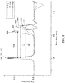
- FIG. 6 illustrates test results obtained from inspection of first sample 132 (shown in FIGS. 4 and 5 ).
- first sample 132 is inspected by directing a first electromagnetic pulse 136, a second electromagnetic pulse 138, and a third electromagnetic pulse 140 towards coating 134 (shown in FIGS. 4 and 5 ).
- First electromagnetic pulse 136 is directed when first sample 132 is oriented at the first rotational angle, as shown in FIG. 1 .
- First electromagnetic pulse 136 reflected from first sample 132 includes a first portion 142 received at a first point in time and a second portion 144 received at a second point in time. The difference in time that first portion 142 and second portion 144 are received defines a first time delay 146.
- second electromagnetic pulse 138 is directed when first sample 132 is oriented at second rotational angle ⁇ , as shown in FIG. 2
- third electromagnetic pulse 140 is directed when first sample 132 is oriented at third rotational angle ⁇ , as shown in FIG. 3 .
- a second time delay 148 is defined by a first portion 150 and a second portion 152 of reflected second electromagnetic pulse 138 received at different points in time
- a third time delay 154 is defined by a first portion 156 and a second portion 158 of reflected third electromagnetic pulse 140 received at different points in time.
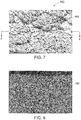
- FIGS. 7 and 8 illustrate top and cross-sectional views of an exemplary second sample 160 that may be inspected with inspection system 100 (shown in FIGS. 1-3 ).
- second sample 160 includes a coating 162 having a second microstructure type that is more random in structure when compared to the first microstructure type shown in FIGS. 4 and 5 , and is thus more isotropic in nature than the first microstructure type.
- FIG. 9 illustrates test results obtained from inspection of second sample 160 (shown in FIGS. 7 and 8 ).
- second sample 160 is inspected by directing a fourth electromagnetic pulse 164, a fifth electromagnetic pulse 166, and a sixth electromagnetic pulse 168 towards coating 162 (shown in FIGS. 7 and 8 ).
- Fourth electromagnetic pulse 164 is directed when second sample 160 is oriented at the first rotational angle, as shown in FIG. 1 .
- Fourth electromagnetic pulse 164 reflected from second sample 160 includes a first portion 170 received at a first point in time and a second portion 172 received at a second point in time. The difference in time that first portion 170 and second portion 172 are received defines a fourth time delay 174.
- fifth electromagnetic pulse 166 is directed when second sample 160 is oriented at second rotational angle ⁇ , as shown in FIG. 2
- sixth electromagnetic pulse 168 is directed when second sample 160 is oriented at third rotational angle ⁇ , as shown in FIG. 3 .
- a fifth time delay 176 is defined by a first portion 178 and a second portion 180 of reflected fifth electromagnetic pulse 166 received at different points in time
- a sixth time delay 182 is defined by a first portion 184 and a second portion 186 of reflected sixth electromagnetic pulse 168 received at different points in time.
- the anisotropic nature of coating 134 causes first time delay 146, second time delay 148, and third time delay 154 to each have different values.
- the isotropic nature of coating 162 causes fourth time delay 174, fifth time delay 176, and sixth time delay 182 to be substantially equal.
- Time delays 146, 148, 154, 174, 176, and 182 may be analyzed to assess the microstructures of coatings 134 and 162.
- computing device 122 shown in FIGS. 1-3
- Computing device 122 may then determine a standard deviation of the time delay values associated with each sample.
- the microstructure of coatings 134 and 162 is determined by comparing the standard deviation associated with each sample to a predetermined threshold. A first microstructure is determined to be present when the standard deviation is greater than the predetermined threshold, and a second microstructure is determined to be present when the standard deviation is less than the predetermined threshold.
- FIG. 10 illustrates test results obtained from inspection of a plurality of samples 108 using inspection system 100 (shown in FIGS. 1-3 ). As shown in FIG. 10 , eight samples 108 were fabricated and evaluated, but it should be understood that any number of samples 108 may be fabricated and evaluated that enables the method of assessing a coating microstructure to function as described herein.
- each sample 108 was evaluated using the inspection system 100 as described above, and the microstructure of coating 112 on each sample 108 is determinable based on a comparison of the time delay data associated with each sample 108. For example, a standard deviation of the time delay data associated with each sample 108 is determined for each sample 108. The standard deviation values are then compared to each other and grouped based on relative differences in the standard deviation values.
- the standard deviation values of samples 3, 4, 5, and 6 are greater than the standard deviation values of samples 1, 2, 7, and 8.
- a first cluster 188 and a second cluster 190 may be defined based on relative differences in the standard deviation values.
- the difference between the highest and lowest standard deviation values contained in either first cluster 188 or second cluster 190 may be a first value
- the difference between the highest standard deviation value in first cluster 188 and the lowest standard deviation value in second cluster may be a second value.
- First cluster 188 and second cluster 190 are defined based on the first value being less than the second value.
- the microstructure of coating 112 on each sample 108 is determined based on inclusion of associated standard deviation values in one of first cluster 188 or second cluster 190.
- samples 3, 4, 5, and 6 are determined to have an anisotropic microstructure
- samples 1, 2, 7, and 8 are determined to have an isotropic microstructure.
- An exemplary technical effect of the systems and methods described herein includes at least one of: (a) non-destructive inspection and determination of coating microstructures; (b) providing an inspection technique with non-ionizing radiation; and (c) providing an inspection technique that is capable of on-wing deployment.
- Exemplary embodiments of systems and methods for use in non-destructive examination of coatings deposited on substrates are not limited to the specific embodiments described herein, but rather, components of systems and/or steps of the methods may be utilized independently and separately from other components and/or steps described herein.
- the methods and systems may also be used in combination with other non-metallic coating systems, and are not limited to practice with only thermal barrier coatings or environmental barrier coatings as described herein. Rather, the exemplary embodiment can be implemented and utilized in connection with many other applications, equipment, and systems that may benefit from the technical effects recited herein.
Landscapes
- Physics & Mathematics (AREA)
- General Physics & Mathematics (AREA)
- Health & Medical Sciences (AREA)
- Life Sciences & Earth Sciences (AREA)
- Chemical & Material Sciences (AREA)
- Analytical Chemistry (AREA)
- Biochemistry (AREA)
- General Health & Medical Sciences (AREA)
- Immunology (AREA)
- Pathology (AREA)
- Spectroscopy & Molecular Physics (AREA)
- Engineering & Computer Science (AREA)
- Radar, Positioning & Navigation (AREA)
- Remote Sensing (AREA)
- Mathematical Physics (AREA)
- Computer Networks & Wireless Communication (AREA)
- Toxicology (AREA)
- Electromagnetism (AREA)
- Investigating Or Analysing Materials By Optical Means (AREA)
- Investigating Materials By The Use Of Optical Means Adapted For Particular Applications (AREA)
Abstract
Description
- The field of the disclosure relates generally to systems and methods of non-destructive examination and, more specifically, to non-destructive examination of single or multi-layer coating structures deposited on substrates.
- Some components, such as hot gas path components of gas turbines, are subjected to high temperatures while in service. At least some such components include a coating system, including a thermal barrier coating and bond coat, on an exterior surface exposed to the high temperatures. The microstructure of many known thermal barrier coatings is dependent on the process parameters of the coating application process. For example, thermal barrier coatings made of the same material may nevertheless have varying microstructures due to variations in the process parameters of the respective coating application processes. Some microstructures are effective at protecting components from exposure to high temperatures, while other microstructures may have a comparatively reduced effectiveness and shorter service life. However, at least some known methods for determining the microstructure of a particular coating are time-consuming and expensive to implement.
- In one aspect, a system for use in inspecting a coating on a substrate is provided. The system includes a platform configured to receive a sample including the substrate having the coating deposited thereon, and a light source configured to direct a plurality of electromagnetic pulses towards a scanning location on the coating, wherein the light source is oriented to direct the plurality of electromagnetic pulses at an oblique angle relative to a surface of the coating. A light detector is configured to receive electromagnetic pulses reflected from the sample, wherein a first portion of each electromagnetic pulse is reflected from the surface of the coating, and a second portion of each electromagnetic pulse is reflected from a surface of the substrate. An actuator is coupled to at least one of the platform and the light source, wherein the actuator is configured to move the platform and the light source relative to each other such that the plurality of electromagnetic pulses are directable towards the scanning location from different rotational positions.
- In another aspect, a method of inspecting a coating on a substrate is provided. The method includes directing a plurality of electromagnetic pulses towards a scanning location on the coating, each electromagnetic pulse directed from a different rotational position relative to the scanning location, and each electromagnetic pulse directed at an oblique angle relative to a surface of the coating. A first portion of each electromagnetic pulse is reflected from the surface of the coating, and a second portion of each electromagnetic pulse is reflected from a surface of the substrate at an interface between the coating and the substrate. The method also includes assessing a time delay between reception of the first portion and the second portion of each reflected electromagnetic pulse at a light detector, thereby defining a plurality of time delays, and analyzing the time delays to assess a microstructure of the coating.
- In yet another aspect, a method of assessing a coating microstructure is provided. The method includes providing a plurality of samples each having a substrate and a coating deposited thereon, evaluating each sample with a plurality of electromagnetic pulses that are each directed from a different rotational position relative to the respective sample, and obtaining time delay data associated with the plurality of electromagnetic pulses being reflected from the plurality of samples. Time delay is defined by receiving a first portion and a second portion of each electromagnetic pulse reflected from each sample at different points in time. The method also includes assessing a microstructure of the coating on the plurality of samples based on a comparison of the time delay data associated with the plurality of samples.
- These and other features, aspects, and advantages of the present disclosure will become better understood when the following detailed description is read with reference to the accompanying drawings in which like characters represent like parts throughout the drawings, wherein:
-
FIG. 1 is a schematic illustration of an exemplary inspection system for use in assessing a coating microstructure, the inspection system in a first mode of operation. -
FIG. 2 is a schematic illustration of the inspection system shown inFIG. 1 after the sample has been rotated by a first angle. -
FIG. 3 is a schematic illustration of the inspection system shown inFIG. 1 after the sample has been rotated by a second angle. -
FIG. 4 illustrates a top view of an exemplary first sample that may be inspected with the system shown inFIGS. 1-3 , the first sample having a first microstructure. -
FIG. 5 illustrates a cross-sectional view of the first sample shown inFIG. 4 , the view taken along Line 5-5. -
FIG. 6 illustrates test results obtained from inspection of the first sample shown inFIG. 4 . -
FIG. 7 illustrates a top view of an exemplary second sample that may be inspected with the system shown inFIGS. 1-3 , the second sample having a second microstructure. -
FIG. 8 illustrates a cross-sectional view of the second sample shown inFIG. 7 , the view taken along Line 8-8. -
FIG. 9 illustrates test results obtained from inspection of the second sample shown inFIG. 7 . -
FIG. 10 illustrates test results obtained from inspection of a plurality of samples using the system shown inFIGS. 1-3 . - Unless otherwise indicated, the drawings provided herein are meant to illustrate features of embodiments of this disclosure. These features are believed to be applicable in a wide variety of systems comprising one or more embodiments of this disclosure. As such, the drawings are not meant to include all conventional features known by those of ordinary skill in the art to be required for the practice of the embodiments disclosed herein.
- In the following specification and the claims, reference will be made to a number of terms, which shall be defined to have the following meanings.
- The singular forms "a", "an", and "the" include plural references unless the context clearly dictates otherwise.
- "Optional" or "optionally" means that the subsequently described event or circumstance may or may not occur, and that the description includes instances where the event occurs and instances where it does not.
- Approximating language, as used herein throughout the specification and claims, may be applied to modify any quantitative representation that could permissibly vary without resulting in a change in the basic function to which it is related. Accordingly, a value modified by a term or terms, such as "about", "approximately", and "substantially", are not to be limited to the precise value specified. In at least some instances, the approximating language may correspond to the precision of an instrument for measuring the value. Here and throughout the specification and claims, range limitations may be combined and/or interchanged, such ranges are identified and include all the sub-ranges contained therein unless context or language indicates otherwise.
- Embodiments of the present disclosure relate to non-destructive examination of single or multi-layer coating structures deposited on substrates. In the exemplary embodiment, the inspection system described herein includes a platform that receives a sample thereon, a light source for directing electromagnetic pulses towards the sample, and a light detector for receiving electromagnetic pulses reflected from the sample. The electromagnetic pulses directed towards the sample have a wavelength in the terahertz frequency range. At this frequency range, the electromagnetic pulses are partially reflected from the air/coating interface at a surface of the coating on the sample, and the rest of the wave travels through the coating and is reflected from the coating/substrate interface. A time delay realized as a result of the difference in travel length of the reflected electromagnetic pulses facilitates estimating a thickness of the coating as well as its refractive index.
- In birefringent materials, the refractive index is dependent on the direction of propagation of an incident beam. Birefringent materials are anisotropic in nature (i.e., they have a defined crystal structure periodicity). In the inspection system described herein, the platform and the light source are moved or rotated relative to each other to enable time delay data to be obtained with the light source positioned at different rotational positions relative to a scanning location on the coating. In many known thermal barrier coatings, two different types of microstructures are typically observed. One is a columnar type, which is more ordered and anisotropic in nature. The other is a cauliflower type, which is more random in structure (i.e., isotropic). It is expected that the time delay will vary in anisotropic materials, and that the time delay will be largely consistent in isotropic materials, as the sample is inspected from the different rotational positions. Using the time delay data obtained from the inspection process, the amount of birefringence contained within a particular sample is determinable, thereby enabling the type of microstructure to be identified in a fast, efficient, and non-destructive manner.
-
FIG. 1 is a schematic illustration of anexemplary inspection system 100 in a first mode of operation. In the exemplary embodiment,inspection system 100 includes aplatform 102, alight source 104, and alight detector 106.Platform 102 receives asample 108 to be inspected thereon.Sample 108 includes asubstrate 110 having acoating 112 deposited thereon.Substrate 110 andcoating 112 may be fabricated of any material that enablesinspection system 100 to function as described herein. Example substrate materials include, but are not limited to, metallic materials that are nickel-based, cobalt-based, and the like. An example coating material includes, but is not limited to, a ceramic material. - In operation,
light source 104 directselectromagnetic pulses 114 towards ascanning location 116 oncoating 112.Light source 104 is oriented to direct the plurality of electromagnetic pulses at an oblique angle θ relative to asurface 118 ofcoating 112. Accordingly,light source 104 is oriented to accurately obtain time delay data from potentially birefringent material having anisotropic microstructures, as described above. The plurality ofelectromagnetic pulses 114 have a wavelength in the terahertz (THz) frequency range defined within a range between about 0.1 THz and about 4 THz. In an alternative embodiment,electromagnetic pulses 114 have a wavelength in any frequency range that enablesinspection system 100 to function as described herein. -
Light detector 106 receiveselectromagnetic pulses 120 reflected fromsample 108. As will be described in more detail below, a first portion of eachelectromagnetic pulse 120 is reflected fromsurface 118 ofcoating 112, and a second portion of eachelectromagnetic pulse 120 is reflected from a surface ofsubstrate 110.Inspection system 100 also includes acomputing device 122 in communication withlight detector 106.Computing device 122 determines a time delay between reception of the first portion and the second portion of each reflectedelectromagnetic pulse 120 atlight detector 106.Computing device 122 may then analyze time delay, forelectromagnetic pulses 114 directed towardssample 108 from different rotational positions, to determine a microstructure ofcoating 112. - For example, at least one of
platform 102 andlight source 104 is coupled to anactuator 124.Actuator 124 movesplatform 102 and/orlight source 104 such that the plurality ofelectromagnetic pulses 114 are directable towardsscanning location 116 from the different rotational positions. More specifically,actuator 124 may be coupled toplatform 102 forrotating platform 102 relative tolight source 104. Alternatively, or additionally,actuator 124 may be coupled tolight source 104 for movinglight source 104 aboutplatform 102. - As shown in
FIG. 1 ,actuator 124 orients sample 108 at a first rotational angle (i.e., 0 degrees) relative to areference axis 126. In operation, first time delay data is obtained whensample 108 is oriented at the first rotational angle, andactuator 124 then orientssample 108 at a second rotational angle α (e.g., 45 degrees) relative to referenceaxis 126, as shown inFIG. 2 . Second time delay data is obtained whensample 108 is oriented at second rotational angle α, andactuator 124 then orientssample 108 at a third rotational angle β (e.g., 90 degrees) relative to referenceaxis 126, as shown inFIG. 3 . Third time delay data is obtained whensample 108 is oriented at third rotational angle β, and the birefringence ofcoating 112 may be determined based on an analysis of the time delay data by computingdevice 122. -
Inspection system 100 also includes ascanning positioner 128 for providing visual positioning guidance onsample 108, which facilitates ensuring thesame scanning location 116 is evaluated byelectromagnetic pulses 114 being directed towardssample 108 from the different rotational positions.Scanning positioner 128 may be any positioning device that enablesinspection system 100 to function as described herein. In the exemplary embodiment,scanning positioner 128 is a laser projection device that provides avisual cue 130 onsurface 118 ofcoating 112 at scanninglocation 116. Accordingly,electromagnetic pulses 114 are directable towards the same location on coating 112 regardless of the relative rotational position oflight source 104 to sample 108. -
FIGS. 4 and 5 illustrate top and cross-sectional views of an exemplaryfirst sample 132 that may be inspected with inspection system 100 (shown inFIGS. 1-3 ). In the exemplary embodiment,first sample 132 includes acoating 134 having a first microstructure type that is columnar, ordered, and thus inherently anisotropic in nature. -
FIG. 6 illustrates test results obtained from inspection of first sample 132 (shown inFIGS. 4 and 5 ). In the exemplary embodiment,first sample 132 is inspected by directing a firstelectromagnetic pulse 136, a secondelectromagnetic pulse 138, and a thirdelectromagnetic pulse 140 towards coating 134 (shown inFIGS. 4 and 5 ). Firstelectromagnetic pulse 136 is directed whenfirst sample 132 is oriented at the first rotational angle, as shown inFIG. 1 . Firstelectromagnetic pulse 136 reflected fromfirst sample 132 includes a first portion 142 received at a first point in time and asecond portion 144 received at a second point in time. The difference in time that first portion 142 andsecond portion 144 are received defines afirst time delay 146. In addition, secondelectromagnetic pulse 138 is directed whenfirst sample 132 is oriented at second rotational angle α, as shown inFIG. 2 , and thirdelectromagnetic pulse 140 is directed whenfirst sample 132 is oriented at third rotational angle β, as shown inFIG. 3 . Asecond time delay 148 is defined by a first portion 150 and asecond portion 152 of reflected secondelectromagnetic pulse 138 received at different points in time, and athird time delay 154 is defined by a first portion 156 and asecond portion 158 of reflected thirdelectromagnetic pulse 140 received at different points in time. -
FIGS. 7 and 8 illustrate top and cross-sectional views of an exemplarysecond sample 160 that may be inspected with inspection system 100 (shown inFIGS. 1-3 ). In the exemplary embodiment,second sample 160 includes acoating 162 having a second microstructure type that is more random in structure when compared to the first microstructure type shown inFIGS. 4 and 5 , and is thus more isotropic in nature than the first microstructure type. -
FIG. 9 illustrates test results obtained from inspection of second sample 160 (shown inFIGS. 7 and 8 ). In the exemplary embodiment,second sample 160 is inspected by directing a fourth electromagnetic pulse 164, a fifth electromagnetic pulse 166, and a sixth electromagnetic pulse 168 towards coating 162 (shown inFIGS. 7 and 8 ). Fourth electromagnetic pulse 164 is directed whensecond sample 160 is oriented at the first rotational angle, as shown inFIG. 1 . Fourth electromagnetic pulse 164 reflected fromsecond sample 160 includes a first portion 170 received at a first point in time and a second portion 172 received at a second point in time. The difference in time that first portion 170 and second portion 172 are received defines a fourth time delay 174. In addition, fifth electromagnetic pulse 166 is directed whensecond sample 160 is oriented at second rotational angle α, as shown inFIG. 2 , and sixth electromagnetic pulse 168 is directed whensecond sample 160 is oriented at third rotational angle β, as shown inFIG. 3 . A fifth time delay 176 is defined by a first portion 178 and a second portion 180 of reflected fifth electromagnetic pulse 166 received at different points in time, and a sixth time delay 182 is defined by a first portion 184 and a second portion 186 of reflected sixth electromagnetic pulse 168 received at different points in time. - As shown in
FIG. 6 , the anisotropic nature of coating 134 (shown inFIGS. 4 and 5 ) causesfirst time delay 146,second time delay 148, andthird time delay 154 to each have different values. In addition, as shown inFIG. 9 , the isotropic nature ofcoating 162 causes fourth time delay 174, fifth time delay 176, and sixth time delay 182 to be substantially equal. Time delays 146, 148, 154, 174, 176, and 182 may be analyzed to assess the microstructures ofcoatings FIGS. 1-3 ) may receive the values oftime delays Computing device 122 may then determine a standard deviation of the time delay values associated with each sample. In one embodiment, the microstructure ofcoatings -
FIG. 10 illustrates test results obtained from inspection of a plurality ofsamples 108 using inspection system 100 (shown inFIGS. 1-3 ). As shown inFIG. 10 , eightsamples 108 were fabricated and evaluated, but it should be understood that any number ofsamples 108 may be fabricated and evaluated that enables the method of assessing a coating microstructure to function as described herein. In the exemplary embodiment, eachsample 108 was evaluated using theinspection system 100 as described above, and the microstructure ofcoating 112 on eachsample 108 is determinable based on a comparison of the time delay data associated with eachsample 108. For example, a standard deviation of the time delay data associated with eachsample 108 is determined for eachsample 108. The standard deviation values are then compared to each other and grouped based on relative differences in the standard deviation values. - In the exemplary embodiment, the standard deviation values of
samples samples first cluster 188 and asecond cluster 190 may be defined based on relative differences in the standard deviation values. For example, the difference between the highest and lowest standard deviation values contained in eitherfirst cluster 188 orsecond cluster 190 may be a first value, and the difference between the highest standard deviation value infirst cluster 188 and the lowest standard deviation value in second cluster may be a second value.First cluster 188 andsecond cluster 190 are defined based on the first value being less than the second value. As such, the microstructure ofcoating 112 on eachsample 108 is determined based on inclusion of associated standard deviation values in one offirst cluster 188 orsecond cluster 190. Thus, according toFIG. 10 ,samples samples - An exemplary technical effect of the systems and methods described herein includes at least one of: (a) non-destructive inspection and determination of coating microstructures; (b) providing an inspection technique with non-ionizing radiation; and (c) providing an inspection technique that is capable of on-wing deployment.
- Exemplary embodiments of systems and methods for use in non-destructive examination of coatings deposited on substrates are not limited to the specific embodiments described herein, but rather, components of systems and/or steps of the methods may be utilized independently and separately from other components and/or steps described herein. For example, the methods and systems may also be used in combination with other non-metallic coating systems, and are not limited to practice with only thermal barrier coatings or environmental barrier coatings as described herein. Rather, the exemplary embodiment can be implemented and utilized in connection with many other applications, equipment, and systems that may benefit from the technical effects recited herein.
- Although specific features of various embodiments of the disclosure may be shown in some drawings and not in others, this is for convenience only. In accordance with the principles of the disclosure, any feature of a drawing may be referenced and/or claimed in combination with any feature of any other drawing.
- This written description uses examples to disclose the embodiments, including the best mode, and also to enable any person skilled in the art to practice the embodiments, including making and using any devices or systems and performing any incorporated methods. The patentable scope of the disclosure is defined by the claims, and may include other examples that occur to those skilled in the art. Such other examples are intended to be within the scope of the claims if they have structural elements that do not differ from the literal language of the claims, or if they include equivalent structural elements with insubstantial differences from the literal language of the claims.
- Further aspects of the invention are provided by the subject matter of the following clauses:
- 1. A system for use in inspecting a coating on a substrate, the system comprising:
- a platform configured to receive a sample including the substrate having the coating deposited thereon;
- a light source configured to direct a plurality of electromagnetic pulses towards a scanning location on the coating, wherein the light source is oriented to direct the plurality of electromagnetic pulses at an oblique angle relative to a surface of the coating;
- a light detector configured to receive electromagnetic pulses reflected from the sample, wherein a first portion of each electromagnetic pulse is reflected from the surface of the coating at an interface between the coating and an ambient environment, and wherein a second portion of each electromagnetic pulse is reflected from a surface of the substrate at an interface between the coating and the substrate; and
- an actuator coupled to at least one of the platform and the light source, wherein the actuator is configured to move the platform and the light source relative to each other such that the plurality of electromagnetic pulses are directable towards the scanning location from different rotational positions.
- 2. The system in accordance with any preceding clause further comprising a computing device in communication with the light detector, the computing device configured to:
- determine a time delay between reception of the first portion and the second portion of each reflected electromagnetic pulse at the light detector, thereby defining a plurality of time delays; and
- analyze the time delays to assess a microstructure of the coating.
- 3. The system in accordance with any preceding clause, wherein the actuator is coupled to the platform, and is configured to rotate the platform relative to the light source.
- 4. The system in accordance with any preceding clause, wherein the actuator is coupled to the light source, and is configured to rotate the light source about the platform.
- 5. A method of inspecting a coating on a substrate, the method comprising:
- directing a plurality of electromagnetic pulses towards a scanning location on the coating, each electromagnetic pulse directed from a different rotational position relative to the scanning location, and each electromagnetic pulse directed at an oblique angle relative to a surface of the coating, wherein a first portion of each electromagnetic pulse is reflected from the surface of the coating, and wherein a second portion of each electromagnetic pulse is reflected from a surface of the substrate at an interface between the coating and the substrate;
- determining a time delay between reception of the first portion and the second portion of each reflected electromagnetic pulse at a light detector, thereby defining a plurality of time delays; and
- analyzing the time delays to assess a microstructure of the coating.
- 6. The method in accordance with any preceding clause, wherein analyzing the time delays comprises determining a standard deviation of the time delay for each of the plurality of electromagnetic pulses.
- 7. The method in accordance with any preceding clause further comprising comparing the standard deviation to a predetermined threshold, wherein a first microstructure is determined when the standard deviation is greater than the predetermined threshold, and wherein a second microstructure is determined when the standard deviation is less than the predetermined threshold.
- 8. The method in accordance with any preceding clause, wherein directing a plurality of electromagnetic pulses comprises directing the plurality of electromagnetic pulses having a wavelength in the terahertz frequency range.
- 9. The method in accordance with any preceding clause, wherein directing a plurality of electromagnetic pulses comprises:
- emitting the plurality of electromagnetic pulses from a light source; and
- rotating at least one of the substrate and the light source.
- 10. The method in accordance with any preceding clause, wherein rotating at least one of the substrate or the light source comprises positioning the light source within a rotational range defined between about 0 degrees and about 360 degrees relative to the scanning location.
- 11. The method in accordance with any preceding clause further comprising:
- providing a visual cue on the coating at the scanning location; and
- directing the plurality of electromagnetic pulses towards the visual cue from each rotational position.
- 12. A method of assessing a coating microstructure, the method comprising:
- providing a plurality of samples each having a substrate and a coating deposited thereon;
- evaluating each sample with a plurality of electromagnetic pulses that are each directed from a different rotational position relative to the respective sample;
- obtaining time delay data associated with the plurality of electromagnetic pulses being reflected from the plurality of samples, wherein a time delay is defined by receiving a first portion and a second portion of each electromagnetic pulse reflected from each sample at different points in time; and
- assessing a microstructure of the coating on the plurality of samples based on a comparison of the time delay data associated with the plurality of samples.
- 13. The method in accordance with any preceding clause, wherein assessing a microstructure comprises:
- determining a standard deviation of the time delay data associated with each sample;
- grouping the standard deviation values based on relative differences in the standard deviation values; and
- assessing the microstructure of the coating of each sample based on the grouping.
- 14. The method in accordance with any preceding clause, wherein grouping the standard deviation values comprises defining a first cluster and a second cluster, the first cluster and the second cluster being separated by a value that is greater than a maximum difference in standard deviation values contained in either the first cluster or the second cluster.
- 15. The method in accordance with any preceding clause, wherein assessing the microstructure comprises:
- determining the microstructure is anisotropic when the standard deviation of a sample is included in the first cluster; and
- determining the microstructure is isotropic when the standard deviation of a sample is included in the second cluster.
- 16. The method in accordance with any preceding clause, wherein evaluating each sample comprises directing the plurality of electromagnetic pulses towards a scanning location on the coating, each electromagnetic pulse directed at an oblique angle relative to a surface of the coating, wherein the first portion of each electromagnetic pulse is reflected from the surface of the coating, and wherein the second portion of each electromagnetic pulse is reflected from a surface of the substrate.
- 17. The method in accordance with any preceding clause, wherein directing a plurality of electromagnetic pulses comprises directing the plurality of electromagnetic pulses having a wavelength in the terahertz frequency range.
- 18. The method in accordance with any preceding clause, wherein directing a plurality of electromagnetic pulses comprises:
- emitting the plurality of electromagnetic pulses from a light source; and
- rotating at least one of the substrate and the light source.
- 19. The method in accordance with any preceding clause, wherein rotating at least one of the substrate or the light source comprises positioning the light source within a rotational range defined between about 0 degrees and about 360 degrees relative to the scanning location.
- 20. The method in accordance with any preceding clause further comprising:
- providing a visual cue on the coating at a scanning location; and
- directing the plurality of electromagnetic pulses towards the visual cue from each rotational position.
Claims (15)
- A system for use in inspecting a coating (112) on a substrate (110), the system comprising:a platform (102) configured to receive a sample (108) including the substrate (110) having the coating (112) deposited thereon;a light source (104) configured to direct a plurality of electromagnetic pulses (114) towards a scanning location (116) on the coating (112), wherein the light source (104) is oriented to direct the plurality of electromagnetic pulses (114) at an oblique angle relative to a surface (118) of the coating (112);a light detector (106) configured to receive electromagnetic pulses (114) reflected from the sample (108), wherein a first portion (142) of each electromagnetic pulse (114) is reflected from the surface (118) of the coating (112) at an interface between the coating (112) and an ambient environment, and wherein a second portion (144) of each electromagnetic pulse (114) is reflected from a surface (118) of the substrate (110) at an interface between the coating (112) and the substrate (110); andan actuator (124) coupled to at least one of the platform (102) and the light source (104), wherein the actuator (124) is configured to move the platform (102) and the light source (104) relative to each other such that the plurality of electromagnetic pulses (114) are directable towards the scanning location (116) from different rotational positions.
- The system in accordance with Claim 1 further comprising a computing device (122) in communication with the light detector (106), the computing device (122) configured to:determine a time delay between reception of the first portion (142) and the second portion (144) of each reflected electromagnetic pulse at the light detector (106), thereby defining a plurality of time delays; andanalyze the time delays to assess a microstructure of the coating (112).
- The system in accordance with Claim 1 or 2, wherein the actuator (124) is coupled to the platform (102), and is configured to rotate the platform (102) relative to the light source (104).
- The system in accordance with any of Claims 1 to 3, wherein the actuator (124) is coupled to the light source (104), and is configured to rotate the light source (104) about the platform (102).
- A method of inspecting a coating (112) on a substrate (110), the method comprising:directing a plurality of electromagnetic pulses (114) towards a scanning location (116) on the coating (112), each electromagnetic pulse (114) directed from a different rotational position relative to the scanning location (116), and each electromagnetic pulse (114) directed at an oblique angle relative to a surface (118) of the coating (112), wherein a first portion (142) of each electromagnetic pulse (114) is reflected from the surface (118) of the coating (112), and wherein a second portion (144) of each electromagnetic pulse (114) is reflected from a surface (118) of the substrate (110) at an interface between the coating (112) and the substrate (110);determining a time delay between reception of the first portion (142) and the second portion (144) of each reflected electromagnetic pulse at a light detector (106), thereby defining a plurality of time delays; andanalyzing the time delays to assess a microstructure of the coating (112).
- The method in accordance with Claim 5, wherein analyzing the time delays comprises determining a standard deviation of the time delay for each of the plurality of electromagnetic pulses (114), the method further comprising comparing the standard deviation to a predetermined threshold, wherein a first microstructure is determined when the standard deviation is greater than the predetermined threshold, and wherein a second microstructure is determined when the standard deviation is less than the predetermined threshold.
- The method in accordance with Claim 5 or 6, wherein directing a plurality of electromagnetic pulses (114) comprises directing the plurality of electromagnetic pulses (114) having a wavelength in the terahertz frequency range.
- The method in accordance with any of Claims 5 to 7, wherein directing a plurality of electromagnetic pulses (114) comprises:emitting the plurality of electromagnetic pulses (114) from a light source (104); androtating at least one of the substrate (110) and the light source (104), wherein rotating at least one of the substrate (110) or the light source (104) comprises positioning the light source (104) within a rotational range defined between about 0 degrees and about 360 degrees relative to the scanning location (116).
- The method in accordance with any of Claims 5 to 8 further comprising:providing a visual cue (130) on the coating (112) at the scanning location (116); anddirecting the plurality of electromagnetic pulses (114) towards the visual cue (130) from each rotational position.
- A method of assessing a coating (112) microstructure, the method comprising:providing a plurality of samples (108) each having a substrate (110) and a coating (112) deposited thereon;evaluating each sample (108) with a plurality of electromagnetic pulses (114) that are each directed from a different rotational position relative to the respective sample (108);obtaining time delay data associated with the plurality of electromagnetic pulses (114) being reflected from the plurality of samples (108), wherein a time delay is defined by receiving a first portion (142) and a second portion (144) of each electromagnetic pulse (114) reflected from each sample (108) at different points in time; andassessing a microstructure of the coating (112) on the plurality of samples (108) based on a comparison of the time delay data associated with the plurality of samples (108).
- The method in accordance with Claim 10, wherein assessing a microstructure comprises:determining a standard deviation of the time delay data associated with each sample (108);grouping the standard deviation values based on relative differences in the standard deviation values; andassessing the microstructure of the coating (112) of each sample (108) based on the grouping.
- The method in accordance with Claim 11, wherein grouping the standard deviation values comprises defining a first cluster (188) and a second cluster (190), the first cluster (188) and the second cluster (190) being separated by a value that is greater than a maximum difference in standard deviation values contained in either the first cluster (188) or the second cluster (190), and wherein assessing the microstructure comprises:determining the microstructure is anisotropic when the standard deviation of a sample (108) is included in the first cluster (188); anddetermining the microstructure is isotropic when the standard deviation of a sample (108) is included in the second cluster (190).
- The method in accordance with any of Claims 10 to 12, wherein evaluating each sample (108) comprises directing the plurality of electromagnetic pulses (114), having a wavelength in the terahertz frequency range, towards a scanning location (116) on the coating (112), each electromagnetic pulse (114) directed at an oblique angle relative to a surface (118) of the coating (112), wherein the first portion (142) of each electromagnetic pulse (114) is reflected from the surface (118) of the coating (112), and wherein the second portion (144) of each electromagnetic pulse (114) is reflected from a surface (118) of the substrate (110).
- The method in accordance with Claim 13, wherein directing a plurality of electromagnetic pulses (114) comprises:emitting the plurality of electromagnetic pulses (114) from a light source (104); androtating at least one of the substrate (110) and the light source (104), wherein rotating at least one of the substrate (110) or the light source (104) comprises positioning the light source (104) within a rotational range defined between about 0 degrees and about 360 degrees relative to the scanning location (116).
- The method in accordance with any of Claims 10 to 14 further comprising:providing a visual cue (130) on the coating (112) at a scanning location (116); anddirecting the plurality of electromagnetic pulses (114) towards the visual cue (130) from each rotational position.
Applications Claiming Priority (1)
| Application Number | Priority Date | Filing Date | Title |
|---|---|---|---|
| US16/707,493 US11099002B2 (en) | 2019-12-09 | 2019-12-09 | Systems and methods of assessing a coating microstructure |
Publications (2)
| Publication Number | Publication Date |
|---|---|
| EP3835760A1 true EP3835760A1 (en) | 2021-06-16 |
| EP3835760B1 EP3835760B1 (en) | 2025-01-29 |
Family
ID=73698665
Family Applications (1)
| Application Number | Title | Priority Date | Filing Date |
|---|---|---|---|
| EP20211590.3A Active EP3835760B1 (en) | 2019-12-09 | 2020-12-03 | Systems and methods of assessing a coating microstructure |
Country Status (4)
| Country | Link |
|---|---|
| US (1) | US11099002B2 (en) |
| EP (1) | EP3835760B1 (en) |
| CN (1) | CN113030127A (en) |
| SG (1) | SG10202012242PA (en) |
Cited By (1)
| Publication number | Priority date | Publication date | Assignee | Title |
|---|---|---|---|---|
| EP4372368A1 (en) * | 2022-11-16 | 2024-05-22 | General Electric Company | Method for determining the microstructure for a coating |
Families Citing this family (1)
| Publication number | Priority date | Publication date | Assignee | Title |
|---|---|---|---|---|
| US20250290859A1 (en) * | 2024-03-12 | 2025-09-18 | General Electric Company | Electromagnetic inspection systems and methods |
Citations (3)
| Publication number | Priority date | Publication date | Assignee | Title |
|---|---|---|---|---|
| GB2446026A (en) * | 2007-01-29 | 2008-07-30 | Teraview Ltd | Analysis apparatus and method |
| US20140264032A1 (en) * | 2013-03-15 | 2014-09-18 | The Johns Hopkins University | Terahertz time-domain spectroscopic ellipsometry system |
| CN208998745U (en) * | 2018-07-21 | 2019-06-18 | 烟台太赫兹光电科技有限公司 | Contactless Terahertz overbrushing layer thickness detection device |
Family Cites Families (15)
| Publication number | Priority date | Publication date | Assignee | Title |
|---|---|---|---|---|
| US3994586A (en) * | 1975-10-30 | 1976-11-30 | Aluminum Company Of America | Simultaneous determination of film uniformity and thickness |
| US20060256916A1 (en) * | 2005-05-13 | 2006-11-16 | Rudolph Technologies, Inc. | Combined ultra-fast x-ray and optical system for thin film measurements |
| US7933027B1 (en) * | 2008-06-27 | 2011-04-26 | The United States Of America As Represented By The Administrator Of National Aeronautics And Space Administration | Processing waveform-based NDE |
| US9017792B2 (en) | 2011-04-30 | 2015-04-28 | Chromalloy Gas Turbine Llc | Tri-barrier ceramic coating |
| DE102011104708A1 (en) * | 2011-06-06 | 2012-12-06 | Automation Dr. Nix Gmbh & Co. Kg | Method and device for determining material properties of a substrate sample in the Tera-Hertz frequency spectrum |
| JP2013174548A (en) * | 2012-02-27 | 2013-09-05 | Otsuka Denshi Co Ltd | Measuring instrument and measuring method |
| US9157730B2 (en) * | 2012-10-26 | 2015-10-13 | Applied Materials, Inc. | PECVD process |
| US20150000405A1 (en) | 2013-06-27 | 2015-01-01 | Honeywell International Inc. | Non-destructive evaluation methods for determining a thickness of a coating layer on a turbine engine component |
| JP6281941B2 (en) | 2014-01-31 | 2018-02-21 | 一般財団法人電力中央研究所 | Dielectric refractive index detection method and apparatus, film thickness detection method and apparatus, and surface roughness detection method and apparatus |
| WO2017173533A1 (en) * | 2016-04-04 | 2017-10-12 | Tetechs Inc. | Methods and systems for thickness measurement of multi-layer structures |
| US10648937B2 (en) | 2016-10-27 | 2020-05-12 | General Electric Company | Nondestructive inspection method for coatings and ceramic matrix composites |
| US10690602B2 (en) * | 2017-02-17 | 2020-06-23 | Kla-Tencor Corporation | Methods and systems for measurement of thick films and high aspect ratio structures |
| US10254219B1 (en) * | 2017-10-27 | 2019-04-09 | Ford Motor Company | System and method for visually aligning terahertz light beam |
| CN108519059B (en) | 2018-04-20 | 2019-06-28 | 中国矿业大学 | Thermal barrier coating multi-layered thickness detection method based on reflection-type terahertz time-domain spectroscopic technology |
| CN109883337A (en) * | 2019-01-25 | 2019-06-14 | 北京航天计量测试技术研究所 | Thermal Barrier Coating Thickness Measurement System and Measurement Method Based on Terahertz Spectroscopy |
-
2019
- 2019-12-09 US US16/707,493 patent/US11099002B2/en active Active
-
2020
- 2020-12-03 EP EP20211590.3A patent/EP3835760B1/en active Active
- 2020-12-08 SG SG10202012242PA patent/SG10202012242PA/en unknown
- 2020-12-09 CN CN202011430848.XA patent/CN113030127A/en active Pending
Patent Citations (3)
| Publication number | Priority date | Publication date | Assignee | Title |
|---|---|---|---|---|
| GB2446026A (en) * | 2007-01-29 | 2008-07-30 | Teraview Ltd | Analysis apparatus and method |
| US20140264032A1 (en) * | 2013-03-15 | 2014-09-18 | The Johns Hopkins University | Terahertz time-domain spectroscopic ellipsometry system |
| CN208998745U (en) * | 2018-07-21 | 2019-06-18 | 烟台太赫兹光电科技有限公司 | Contactless Terahertz overbrushing layer thickness detection device |
Non-Patent Citations (5)
| Title |
|---|
| ELLRICH F ET AL: "Terahertz Quality Inspection for Automotive and Aviation Industries", JOURNAL OF INFRARED, MILLIMETER AND TERAHERTZ WAVES, SPRINGER NEW YORK LLC, US, vol. 41, no. 4, 26 November 2019 (2019-11-26), pages 470 - 489, XP037106915, ISSN: 1866-6892, [retrieved on 20191126], DOI: 10.1007/S10762-019-00639-4 * |
| KRIMI S ET AL: "Self-calibrating approach for terahertz thickness measurements of ceramic coatings", 2016 41ST INTERNATIONAL CONFERENCE ON INFRARED, MILLIMETER, AND TERAHERTZ WAVES (IRMMW-THZ), IEEE, 25 September 2016 (2016-09-25), pages 1 - 2, XP033010254, DOI: 10.1109/IRMMW-THZ.2016.7758545 * |
| LOPATO PRZEMYSLAW: "Double-Sided Terahertz Imaging of Multilayered Glass Fiber-Reinforced Polymer", APPLIED SCIENCES, vol. 7, no. 7, 27 June 2017 (2017-06-27), pages 661, XP055789422, DOI: 10.3390/app7070661 * |
| QIU F C ET AL: "Fast terahertz reflective confocal scanning imaging with a quantum cascade laser and a photodetector", APPLIED PHYSICS B: LASERS AND OPTICS, SPRINGER INTERNATIONAL, BERLIN, DE, vol. 125, no. 5, 2 May 2019 (2019-05-02), pages 1 - 8, XP036779575, ISSN: 0946-2171, [retrieved on 20190502], DOI: 10.1007/S00340-019-7198-8 * |
| TU WANLI ET AL: "FDTD-based quantitative analysis of terahertz wave detection for multilayered structures", JOURNAL OF THE OPTICAL SOCIETY OF AMERICA A, vol. 31, no. 10, 24 September 2014 (2014-09-24), pages 2285, XP055789427, ISSN: 1084-7529, DOI: 10.1364/JOSAA.31.002285 * |
Cited By (1)
| Publication number | Priority date | Publication date | Assignee | Title |
|---|---|---|---|---|
| EP4372368A1 (en) * | 2022-11-16 | 2024-05-22 | General Electric Company | Method for determining the microstructure for a coating |
Also Published As
| Publication number | Publication date |
|---|---|
| SG10202012242PA (en) | 2021-07-29 |
| EP3835760B1 (en) | 2025-01-29 |
| CN113030127A (en) | 2021-06-25 |
| US20210172726A1 (en) | 2021-06-10 |
| US11099002B2 (en) | 2021-08-24 |
Similar Documents
| Publication | Publication Date | Title |
|---|---|---|
| US10648937B2 (en) | Nondestructive inspection method for coatings and ceramic matrix composites | |
| Bates et al. | Rapid thermal non-destructive testing of aircraft components | |
| US8300232B2 (en) | Method of measuring coating thickness using infrared light | |
| EP2899498A1 (en) | Sensor system and method for characterizing a coated body | |
| JP6281941B2 (en) | Dielectric refractive index detection method and apparatus, film thickness detection method and apparatus, and surface roughness detection method and apparatus | |
| US10274367B2 (en) | Deconvolution to reduce the effective spot size of a spectroscopic optical metrology device | |
| Yule et al. | Surface temperature condition monitoring methods for aerospace turbomachinery: Exploring the use of ultrasonic guided waves | |
| Akbar et al. | Nondestructive evaluation of coatings delamination using microwave time domain reflectometry technique | |
| US11099002B2 (en) | Systems and methods of assessing a coating microstructure | |
| CN105572229B (en) | Method for verifying the calibration of a non-destructive testing system for components and assembly | |
| Fukuchi et al. | Measurement of topcoat thickness of thermal barrier coating for gas turbines using terahertz waves | |
| Shaklan et al. | Solar glint from uncoated starshade optical edges | |
| An et al. | Defect visualization of cylindrical and conical CFRP lattice structures using rotational ultrasonic propagation imager | |
| Picot et al. | Terahertz Paint Thickness Measurements: from lab to automotive and aeronautics industry | |
| Wang et al. | Iterative alignment of reflector panels for large-scale compact test range in non-metrology environment based on laser tracker | |
| KR101664470B1 (en) | Multiple beam path optical system using rear surface reflection of beam splitter | |
| CN107817256A (en) | A kind of lossless detection method for optical crystal Ultra-precision Turning sub-surface damage | |
| Apeksimov et al. | Nondestructive Testing of Civil Aircraft Turbojet Engine Blades with LIBS | |
| Luo et al. | Non-contact thickness measurement of coatings on metallic substrate using pulsed terahertz technology | |
| Waldstein et al. | Microwave Photoelasticity: Exploiting Multiple Resonances to Measure Stress Changes within Yttria-Partially-Stabilized-Zirconia | |
| CN119879751B (en) | A method for extracting the thickness of multilayer coatings on anisotropic substrates | |
| CN113640327B (en) | Nondestructive testing method for multi-layer metal film on surface of large-curvature micro part | |
| OPPELT et al. | 3D-SAR-Imaging and Thickness Determination of Zirconia Based Coatings on Non-Planar Metal Substrates in the Lower Terahertz Region | |
| KR101609548B1 (en) | Multiple beam path laser optical system by multiple-beam reflector | |
| Ying | Application of millimeter-wave differential probe for crack detection on riveted structures |
Legal Events
| Date | Code | Title | Description |
|---|---|---|---|
| PUAI | Public reference made under article 153(3) epc to a published international application that has entered the european phase |
Free format text: ORIGINAL CODE: 0009012 |
|
| STAA | Information on the status of an ep patent application or granted ep patent |
Free format text: STATUS: THE APPLICATION HAS BEEN PUBLISHED |
|
| AK | Designated contracting states |
Kind code of ref document: A1 Designated state(s): AL AT BE BG CH CY CZ DE DK EE ES FI FR GB GR HR HU IE IS IT LI LT LU LV MC MK MT NL NO PL PT RO RS SE SI SK SM TR |
|
| STAA | Information on the status of an ep patent application or granted ep patent |
Free format text: STATUS: REQUEST FOR EXAMINATION WAS MADE |
|
| 17P | Request for examination filed |
Effective date: 20211209 |
|
| RBV | Designated contracting states (corrected) |
Designated state(s): AL AT BE BG CH CY CZ DE DK EE ES FI FR GB GR HR HU IE IS IT LI LT LU LV MC MK MT NL NO PL PT RO RS SE SI SK SM TR |
|
| STAA | Information on the status of an ep patent application or granted ep patent |
Free format text: STATUS: EXAMINATION IS IN PROGRESS |
|
| 17Q | First examination report despatched |
Effective date: 20230217 |
|
| GRAP | Despatch of communication of intention to grant a patent |
Free format text: ORIGINAL CODE: EPIDOSNIGR1 |
|
| STAA | Information on the status of an ep patent application or granted ep patent |
Free format text: STATUS: GRANT OF PATENT IS INTENDED |
|
| INTG | Intention to grant announced |
Effective date: 20240725 |
|
| GRAS | Grant fee paid |
Free format text: ORIGINAL CODE: EPIDOSNIGR3 |
|
| GRAA | (expected) grant |
Free format text: ORIGINAL CODE: 0009210 |
|
| STAA | Information on the status of an ep patent application or granted ep patent |
Free format text: STATUS: THE PATENT HAS BEEN GRANTED |
|
| RAP3 | Party data changed (applicant data changed or rights of an application transferred) |
Owner name: GENERAL ELECTRIC COMPANY |
|
| P01 | Opt-out of the competence of the unified patent court (upc) registered |
Free format text: CASE NUMBER: APP_65784/2024 Effective date: 20241212 |
|
| AK | Designated contracting states |
Kind code of ref document: B1 Designated state(s): AL AT BE BG CH CY CZ DE DK EE ES FI FR GB GR HR HU IE IS IT LI LT LU LV MC MK MT NL NO PL PT RO RS SE SI SK SM TR |
|
| REG | Reference to a national code |
Ref country code: GB Ref legal event code: FG4D |
|
| REG | Reference to a national code |
Ref country code: CH Ref legal event code: EP |
|
| REG | Reference to a national code |
Ref country code: DE Ref legal event code: R096 Ref document number: 602020045449 Country of ref document: DE |
|
| REG | Reference to a national code |
Ref country code: IE Ref legal event code: FG4D |
|
| REG | Reference to a national code |
Ref country code: NL Ref legal event code: MP Effective date: 20250129 |
|
| PG25 | Lapsed in a contracting state [announced via postgrant information from national office to epo] |
Ref country code: NL Free format text: LAPSE BECAUSE OF FAILURE TO SUBMIT A TRANSLATION OF THE DESCRIPTION OR TO PAY THE FEE WITHIN THE PRESCRIBED TIME-LIMIT Effective date: 20250129 |
|
| PG25 | Lapsed in a contracting state [announced via postgrant information from national office to epo] |
Ref country code: RS Free format text: LAPSE BECAUSE OF FAILURE TO SUBMIT A TRANSLATION OF THE DESCRIPTION OR TO PAY THE FEE WITHIN THE PRESCRIBED TIME-LIMIT Effective date: 20250429 |
|
| PG25 | Lapsed in a contracting state [announced via postgrant information from national office to epo] |
Ref country code: FI Free format text: LAPSE BECAUSE OF FAILURE TO SUBMIT A TRANSLATION OF THE DESCRIPTION OR TO PAY THE FEE WITHIN THE PRESCRIBED TIME-LIMIT Effective date: 20250129 |
|
| PG25 | Lapsed in a contracting state [announced via postgrant information from national office to epo] |
Ref country code: PL Free format text: LAPSE BECAUSE OF FAILURE TO SUBMIT A TRANSLATION OF THE DESCRIPTION OR TO PAY THE FEE WITHIN THE PRESCRIBED TIME-LIMIT Effective date: 20250129 |
|
| PG25 | Lapsed in a contracting state [announced via postgrant information from national office to epo] |
Ref country code: ES Free format text: LAPSE BECAUSE OF FAILURE TO SUBMIT A TRANSLATION OF THE DESCRIPTION OR TO PAY THE FEE WITHIN THE PRESCRIBED TIME-LIMIT Effective date: 20250129 |
|
| REG | Reference to a national code |
Ref country code: LT Ref legal event code: MG9D |
|
| PG25 | Lapsed in a contracting state [announced via postgrant information from national office to epo] |
Ref country code: IS Free format text: LAPSE BECAUSE OF FAILURE TO SUBMIT A TRANSLATION OF THE DESCRIPTION OR TO PAY THE FEE WITHIN THE PRESCRIBED TIME-LIMIT Effective date: 20250529 Ref country code: NO Free format text: LAPSE BECAUSE OF FAILURE TO SUBMIT A TRANSLATION OF THE DESCRIPTION OR TO PAY THE FEE WITHIN THE PRESCRIBED TIME-LIMIT Effective date: 20250429 |
|
| REG | Reference to a national code |
Ref country code: AT Ref legal event code: MK05 Ref document number: 1763909 Country of ref document: AT Kind code of ref document: T Effective date: 20250129 |
|
| PG25 | Lapsed in a contracting state [announced via postgrant information from national office to epo] |
Ref country code: HR Free format text: LAPSE BECAUSE OF FAILURE TO SUBMIT A TRANSLATION OF THE DESCRIPTION OR TO PAY THE FEE WITHIN THE PRESCRIBED TIME-LIMIT Effective date: 20250129 |
|
| PG25 | Lapsed in a contracting state [announced via postgrant information from national office to epo] |
Ref country code: LV Free format text: LAPSE BECAUSE OF FAILURE TO SUBMIT A TRANSLATION OF THE DESCRIPTION OR TO PAY THE FEE WITHIN THE PRESCRIBED TIME-LIMIT Effective date: 20250129 Ref country code: PT Free format text: LAPSE BECAUSE OF FAILURE TO SUBMIT A TRANSLATION OF THE DESCRIPTION OR TO PAY THE FEE WITHIN THE PRESCRIBED TIME-LIMIT Effective date: 20250529 |
|
| PG25 | Lapsed in a contracting state [announced via postgrant information from national office to epo] |
Ref country code: GR Free format text: LAPSE BECAUSE OF FAILURE TO SUBMIT A TRANSLATION OF THE DESCRIPTION OR TO PAY THE FEE WITHIN THE PRESCRIBED TIME-LIMIT Effective date: 20250430 Ref country code: BG Free format text: LAPSE BECAUSE OF FAILURE TO SUBMIT A TRANSLATION OF THE DESCRIPTION OR TO PAY THE FEE WITHIN THE PRESCRIBED TIME-LIMIT Effective date: 20250129 |
|
| PG25 | Lapsed in a contracting state [announced via postgrant information from national office to epo] |
Ref country code: AT Free format text: LAPSE BECAUSE OF FAILURE TO SUBMIT A TRANSLATION OF THE DESCRIPTION OR TO PAY THE FEE WITHIN THE PRESCRIBED TIME-LIMIT Effective date: 20250129 |
|
| PG25 | Lapsed in a contracting state [announced via postgrant information from national office to epo] |
Ref country code: SE Free format text: LAPSE BECAUSE OF FAILURE TO SUBMIT A TRANSLATION OF THE DESCRIPTION OR TO PAY THE FEE WITHIN THE PRESCRIBED TIME-LIMIT Effective date: 20250129 |
|
| PG25 | Lapsed in a contracting state [announced via postgrant information from national office to epo] |
Ref country code: SM Free format text: LAPSE BECAUSE OF FAILURE TO SUBMIT A TRANSLATION OF THE DESCRIPTION OR TO PAY THE FEE WITHIN THE PRESCRIBED TIME-LIMIT Effective date: 20250129 |
|
| PG25 | Lapsed in a contracting state [announced via postgrant information from national office to epo] |
Ref country code: DK Free format text: LAPSE BECAUSE OF FAILURE TO SUBMIT A TRANSLATION OF THE DESCRIPTION OR TO PAY THE FEE WITHIN THE PRESCRIBED TIME-LIMIT Effective date: 20250129 |
|
| PG25 | Lapsed in a contracting state [announced via postgrant information from national office to epo] |
Ref country code: IT Free format text: LAPSE BECAUSE OF FAILURE TO SUBMIT A TRANSLATION OF THE DESCRIPTION OR TO PAY THE FEE WITHIN THE PRESCRIBED TIME-LIMIT Effective date: 20250129 |
|
| PG25 | Lapsed in a contracting state [announced via postgrant information from national office to epo] |
Ref country code: EE Free format text: LAPSE BECAUSE OF FAILURE TO SUBMIT A TRANSLATION OF THE DESCRIPTION OR TO PAY THE FEE WITHIN THE PRESCRIBED TIME-LIMIT Effective date: 20250129 Ref country code: CZ Free format text: LAPSE BECAUSE OF FAILURE TO SUBMIT A TRANSLATION OF THE DESCRIPTION OR TO PAY THE FEE WITHIN THE PRESCRIBED TIME-LIMIT Effective date: 20250129 |
|
| PG25 | Lapsed in a contracting state [announced via postgrant information from national office to epo] |
Ref country code: RO Free format text: LAPSE BECAUSE OF FAILURE TO SUBMIT A TRANSLATION OF THE DESCRIPTION OR TO PAY THE FEE WITHIN THE PRESCRIBED TIME-LIMIT Effective date: 20250129 |
|
| PG25 | Lapsed in a contracting state [announced via postgrant information from national office to epo] |
Ref country code: SK Free format text: LAPSE BECAUSE OF FAILURE TO SUBMIT A TRANSLATION OF THE DESCRIPTION OR TO PAY THE FEE WITHIN THE PRESCRIBED TIME-LIMIT Effective date: 20250129 |
|
| REG | Reference to a national code |
Ref country code: DE Ref legal event code: R097 Ref document number: 602020045449 Country of ref document: DE |
|
| PLBE | No opposition filed within time limit |
Free format text: ORIGINAL CODE: 0009261 |
|
| STAA | Information on the status of an ep patent application or granted ep patent |
Free format text: STATUS: NO OPPOSITION FILED WITHIN TIME LIMIT |
|
| 26N | No opposition filed |
Effective date: 20251030 |
|
| PGFP | Annual fee paid to national office [announced via postgrant information from national office to epo] |
Ref country code: DE Payment date: 20251126 Year of fee payment: 6 |
|
| PGFP | Annual fee paid to national office [announced via postgrant information from national office to epo] |
Ref country code: GB Payment date: 20251119 Year of fee payment: 6 |
|
| PGFP | Annual fee paid to national office [announced via postgrant information from national office to epo] |
Ref country code: FR Payment date: 20251120 Year of fee payment: 6 |