EP3833166A1 - Hub - Google Patents
Hub Download PDFInfo
- Publication number
- EP3833166A1 EP3833166A1 EP19217235.1A EP19217235A EP3833166A1 EP 3833166 A1 EP3833166 A1 EP 3833166A1 EP 19217235 A EP19217235 A EP 19217235A EP 3833166 A1 EP3833166 A1 EP 3833166A1
- Authority
- EP
- European Patent Office
- Prior art keywords
- housing
- circuit board
- connector
- hub according
- wireless
- Prior art date
- Legal status (The legal status is an assumption and is not a legal conclusion. Google has not performed a legal analysis and makes no representation as to the accuracy of the status listed.)
- Withdrawn
Links
- 230000002093 peripheral effect Effects 0.000 description 5
- 230000005540 biological transmission Effects 0.000 description 1
Images


Classifications
-
- H—ELECTRICITY
- H01—ELECTRIC ELEMENTS
- H01R—ELECTRICALLY-CONDUCTIVE CONNECTIONS; STRUCTURAL ASSOCIATIONS OF A PLURALITY OF MUTUALLY-INSULATED ELECTRICAL CONNECTING ELEMENTS; COUPLING DEVICES; CURRENT COLLECTORS
- H01R13/00—Details of coupling devices of the kinds covered by groups H01R12/70 or H01R24/00 - H01R33/00
- H01R13/46—Bases; Cases
- H01R13/514—Bases; Cases composed as a modular blocks or assembly, i.e. composed of co-operating parts provided with contact members or holding contact members between them
-
- H—ELECTRICITY
- H05—ELECTRIC TECHNIQUES NOT OTHERWISE PROVIDED FOR
- H05K—PRINTED CIRCUITS; CASINGS OR CONSTRUCTIONAL DETAILS OF ELECTRIC APPARATUS; MANUFACTURE OF ASSEMBLAGES OF ELECTRICAL COMPONENTS
- H05K5/00—Casings, cabinets or drawers for electric apparatus
- H05K5/0021—Side-by-side or stacked arrangements
-
- G—PHYSICS
- G06—COMPUTING; CALCULATING OR COUNTING
- G06F—ELECTRIC DIGITAL DATA PROCESSING
- G06F1/00—Details not covered by groups G06F3/00 - G06F13/00 and G06F21/00
- G06F1/16—Constructional details or arrangements
- G06F1/1613—Constructional details or arrangements for portable computers
- G06F1/1632—External expansion units, e.g. docking stations
-
- H—ELECTRICITY
- H01—ELECTRIC ELEMENTS
- H01R—ELECTRICALLY-CONDUCTIVE CONNECTIONS; STRUCTURAL ASSOCIATIONS OF A PLURALITY OF MUTUALLY-INSULATED ELECTRICAL CONNECTING ELEMENTS; COUPLING DEVICES; CURRENT COLLECTORS
- H01R12/00—Structural associations of a plurality of mutually-insulated electrical connecting elements, specially adapted for printed circuits, e.g. printed circuit boards [PCB], flat or ribbon cables, or like generally planar structures, e.g. terminal strips, terminal blocks; Coupling devices specially adapted for printed circuits, flat or ribbon cables, or like generally planar structures; Terminals specially adapted for contact with, or insertion into, printed circuits, flat or ribbon cables, or like generally planar structures
- H01R12/70—Coupling devices
- H01R12/71—Coupling devices for rigid printing circuits or like structures
- H01R12/75—Coupling devices for rigid printing circuits or like structures connecting to cables except for flat or ribbon cables
-
- H—ELECTRICITY
- H01—ELECTRIC ELEMENTS
- H01R—ELECTRICALLY-CONDUCTIVE CONNECTIONS; STRUCTURAL ASSOCIATIONS OF A PLURALITY OF MUTUALLY-INSULATED ELECTRICAL CONNECTING ELEMENTS; COUPLING DEVICES; CURRENT COLLECTORS
- H01R13/00—Details of coupling devices of the kinds covered by groups H01R12/70 or H01R24/00 - H01R33/00
- H01R13/66—Structural association with built-in electrical component
- H01R13/665—Structural association with built-in electrical component with built-in electronic circuit
- H01R13/6691—Structural association with built-in electrical component with built-in electronic circuit with built-in signalling means
-
- H—ELECTRICITY
- H01—ELECTRIC ELEMENTS
- H01R—ELECTRICALLY-CONDUCTIVE CONNECTIONS; STRUCTURAL ASSOCIATIONS OF A PLURALITY OF MUTUALLY-INSULATED ELECTRICAL CONNECTING ELEMENTS; COUPLING DEVICES; CURRENT COLLECTORS
- H01R13/00—Details of coupling devices of the kinds covered by groups H01R12/70 or H01R24/00 - H01R33/00
- H01R13/66—Structural association with built-in electrical component
- H01R13/70—Structural association with built-in electrical component with built-in switch
-
- H—ELECTRICITY
- H01—ELECTRIC ELEMENTS
- H01R—ELECTRICALLY-CONDUCTIVE CONNECTIONS; STRUCTURAL ASSOCIATIONS OF A PLURALITY OF MUTUALLY-INSULATED ELECTRICAL CONNECTING ELEMENTS; COUPLING DEVICES; CURRENT COLLECTORS
- H01R13/00—Details of coupling devices of the kinds covered by groups H01R12/70 or H01R24/00 - H01R33/00
- H01R13/66—Structural association with built-in electrical component
- H01R13/717—Structural association with built-in electrical component with built-in light source
- H01R13/7175—Light emitting diodes (LEDs)
-
- H—ELECTRICITY
- H01—ELECTRIC ELEMENTS
- H01R—ELECTRICALLY-CONDUCTIVE CONNECTIONS; STRUCTURAL ASSOCIATIONS OF A PLURALITY OF MUTUALLY-INSULATED ELECTRICAL CONNECTING ELEMENTS; COUPLING DEVICES; CURRENT COLLECTORS
- H01R27/00—Coupling parts adapted for co-operation with two or more dissimilar counterparts
- H01R27/02—Coupling parts adapted for co-operation with two or more dissimilar counterparts for simultaneous co-operation with two or more dissimilar counterparts
-
- H—ELECTRICITY
- H05—ELECTRIC TECHNIQUES NOT OTHERWISE PROVIDED FOR
- H05K—PRINTED CIRCUITS; CASINGS OR CONSTRUCTIONAL DETAILS OF ELECTRIC APPARATUS; MANUFACTURE OF ASSEMBLAGES OF ELECTRICAL COMPONENTS
- H05K1/00—Printed circuits
- H05K1/18—Printed circuits structurally associated with non-printed electric components
-
- H—ELECTRICITY
- H05—ELECTRIC TECHNIQUES NOT OTHERWISE PROVIDED FOR
- H05K—PRINTED CIRCUITS; CASINGS OR CONSTRUCTIONAL DETAILS OF ELECTRIC APPARATUS; MANUFACTURE OF ASSEMBLAGES OF ELECTRICAL COMPONENTS
- H05K5/00—Casings, cabinets or drawers for electric apparatus
- H05K5/02—Details
- H05K5/0247—Electrical details of casings, e.g. terminals, passages for cables or wiring
-
- H—ELECTRICITY
- H01—ELECTRIC ELEMENTS
- H01R—ELECTRICALLY-CONDUCTIVE CONNECTIONS; STRUCTURAL ASSOCIATIONS OF A PLURALITY OF MUTUALLY-INSULATED ELECTRICAL CONNECTING ELEMENTS; COUPLING DEVICES; CURRENT COLLECTORS
- H01R2201/00—Connectors or connections adapted for particular applications
- H01R2201/06—Connectors or connections adapted for particular applications for computer periphery
-
- H—ELECTRICITY
- H05—ELECTRIC TECHNIQUES NOT OTHERWISE PROVIDED FOR
- H05K—PRINTED CIRCUITS; CASINGS OR CONSTRUCTIONAL DETAILS OF ELECTRIC APPARATUS; MANUFACTURE OF ASSEMBLAGES OF ELECTRICAL COMPONENTS
- H05K2201/00—Indexing scheme relating to printed circuits covered by H05K1/00
- H05K2201/10—Details of components or other objects attached to or integrated in a printed circuit board
- H05K2201/10007—Types of components
- H05K2201/10098—Components for radio transmission, e.g. radio frequency identification [RFID] tag, printed or non-printed antennas
-
- H—ELECTRICITY
- H05—ELECTRIC TECHNIQUES NOT OTHERWISE PROVIDED FOR
- H05K—PRINTED CIRCUITS; CASINGS OR CONSTRUCTIONAL DETAILS OF ELECTRIC APPARATUS; MANUFACTURE OF ASSEMBLAGES OF ELECTRICAL COMPONENTS
- H05K2201/00—Indexing scheme relating to printed circuits covered by H05K1/00
- H05K2201/10—Details of components or other objects attached to or integrated in a printed circuit board
- H05K2201/10007—Types of components
- H05K2201/10189—Non-printed connector
-
- H—ELECTRICITY
- H05—ELECTRIC TECHNIQUES NOT OTHERWISE PROVIDED FOR
- H05K—PRINTED CIRCUITS; CASINGS OR CONSTRUCTIONAL DETAILS OF ELECTRIC APPARATUS; MANUFACTURE OF ASSEMBLAGES OF ELECTRICAL COMPONENTS
- H05K2201/00—Indexing scheme relating to printed circuits covered by H05K1/00
- H05K2201/10—Details of components or other objects attached to or integrated in a printed circuit board
- H05K2201/10227—Other objects, e.g. metallic pieces
- H05K2201/10356—Cables
-
- H—ELECTRICITY
- H05—ELECTRIC TECHNIQUES NOT OTHERWISE PROVIDED FOR
- H05K—PRINTED CIRCUITS; CASINGS OR CONSTRUCTIONAL DETAILS OF ELECTRIC APPARATUS; MANUFACTURE OF ASSEMBLAGES OF ELECTRICAL COMPONENTS
- H05K2201/00—Indexing scheme relating to printed circuits covered by H05K1/00
- H05K2201/10—Details of components or other objects attached to or integrated in a printed circuit board
- H05K2201/10431—Details of mounted components
- H05K2201/10507—Involving several components
- H05K2201/10522—Adjacent components
Landscapes
- Engineering & Computer Science (AREA)
- Microelectronics & Electronic Packaging (AREA)
- Physics & Mathematics (AREA)
- Theoretical Computer Science (AREA)
- Computer Hardware Design (AREA)
- Human Computer Interaction (AREA)
- General Engineering & Computer Science (AREA)
- General Physics & Mathematics (AREA)
- Optics & Photonics (AREA)
- Details Of Connecting Devices For Male And Female Coupling (AREA)
- Telephone Set Structure (AREA)
Abstract
Description
- The present disclosure generally relates to hubs, and particularly to a hub having a first member and a second member that are detachably connected to each other.
- Hubs that connect peripheral devices to a host (e.g., a computer) via cables are known. The length of the cables is an important factor. Long cables allow the hubs to be put at a place that is far away from the host. However, long cables take up more space and are not convenient to carry.
- The invention is defined by the appended claim 1 and the appended claims linked to this claim 1 define additional features of specific embodiments.
- Many aspects of the present embodiments can be better understood with reference to the following drawings. The components in the drawings are not necessarily drawn to scale, the emphasis instead being placed upon clearly illustrating the principles of the present embodiments. Moreover, in the drawings, all the views are schematic, and like reference numerals designate corresponding parts throughout the several views.
-
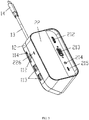
FIG. 1 is an isometric exploded view of a hub according to an embodiment. -
FIG. 2 is the isometric view of the hub ofFIG. 1 , showing that a first member is disengaged from the second member of the hub. -
FIG. 3 is isometric view of the hub ofFIG. 1 , showing that the first member is connected to the second member of the hub. -
FIG. 4 is similar toFIG. 1 , but viewed from a different perspective. - The disclosure is illustrated by way of example and not by way of limitation in the figures of the accompanying drawings, in which like reference numerals indicate similar elements. It should be noted that references to "an" or "one" embodiment in this disclosure are not necessarily to the same embodiment, and such references can mean "at least one" embodiment.
- The terms "upper", "lower", "left" and "right", indicating the orientational or positional relationship based on the orientational or positional relationship shown in the drawings, are merely for convenience of description, but are not intended to indicate or imply that the device or elements must have a particular orientation or be constructed and operated in a particular orientation, and therefore should not be construed as limiting the present invention. The terms "first" and "second" are used for descriptive purposes only and are not to be construed as indicating or implying relative importance or implicitly indicating the number of technical features. The meaning of "multiple" is two or more, unless expressly stated otherwise.
- Referring to
FIGS. 1-4 , in one embodiment, a hub includes afirst member 10 and asecond member 20. The first member includes afirst housing 12 and afirst circuit board 11 arranged within thefirst housing 12. Thefirst circuit board 11 includes awireless emitting module 111. Thesecond member 20 is detachably connected to thefirst member 10 and includes asecond housing 22 and asecond circuit board 21 arranged within thesecond housing 22. Thesecond circuit board 21 includes awireless receiving module 211 that is able to wirelessly communicate with thewireless emitting module 111. - In one embodiment, the
wireless emitting module 111 is an RV110G chip that is electrically connected to thefirst circuit board 11. Thewireless receiving module 211 is a RK3036 chip that is electrically connected to thesecond circuit board 21. Thewireless emitting module 111 and thewireless receiving module 211 uniquely correspond to each other, and they work on the 2.4GHz band or the 5GHz band and can wirelessly communicate with each other. During operation, thefirst member 10 is electrically connected to an electronic device (e.g., a computer), thesecond member 20 is electrically connected to a peripheral device (e.g., a display), and a wireless connection between thefirst member 10 and thesecond member 20 enables the electronic device to be wirelessly connected with the peripheral device, thereby enabling data transmission between the electronic device and the peripheral device. Since thefirst member 10 can be removed from thesecond member 20, they can be placed at different locations, which gives a user the flexibility to place the peripheral device and the electronic device as needed. - In one embodiment, the
first housing 12 includes afirst button 121 that is connected to thefirst circuit board 11 and used to receive a manual operation from a user to enable or disable thewireless emitting module 111. - In one embodiment, the
second housing 22 includes asecond button 221 that is connected to thesecond circuit board 21 and used to receive a manual operation from a user to enable or disable thewireless receiving module 211. When thewireless emitting module 111 and thewireless receiving module 211 are both enabled, they will be automatically paired to form a wireless connection. - In one embodiment, the
first member 10 further includes acable 13 and aplug 14. Thecable 13 includes a first end electrically connected to thefirst circuit board 11, and a second end connected to theplug 14. - In one embodiment, the
plug 14 is a USB type-C male connector. Thecable 13 is electrically connected to theplug 14, and the cable is electrically connected to thefirst circuit board 11. When theplug 14 is inserted into a receptacle of the electronic device, thefirst member 10 is electrically connected to the electronic device. - In one embodiment, the
first member 10 further includes afirst connection member 15 arranged within thefirst housing 12. Thesecond member 20 further includes asecond connection member 23 arranged within thesecond housing 22. Thesecond connection member 23 is can be magnetically connected to thefirst connection member 15, which allows thesecond member 20 to be detachably connected to thefirst member 10. - In the embodiment, the
first connection member 15 can be firmly attracted to thesecond connection member 23, which allows thefirst member 10 and thesecond member 20 to be firmly connected to each other. Thefirst member 10 and thesecond member 20 will not be separated without external force. - In one embodiment, the
second housing 22 defines arecess 222 to receive thefirst housing 12 therein. With such arrangement, thefirst member 10 can steadily rest on thesecond member 20. - In the embodiment, the
recess 222 restricts the movement of thefirst member 10 on thesecond member 20. When thefirst member 10 and thesecond member 20 are attracted to each other, therecess 222 provides more restriction to thefirst member 10. - In one embodiment, the
first circuit board 11 further includes aTF connector 112, anSD connector 114, and a USBfemale connector 113. Thefirst housing 12 defines a first throughhole 122 for theTF connector 112, a second throughhole 123 for theSD connector 114, and a third throughhole 124 for the USBfemale connector 113. These through holes allow corresponding connectors to be exposed so that they can connect with TF cards, SD cards, and USB male connectors. In the embodiment, theTF connector 112, theSD connector 114, and the USBfemale connector 113 are all fixedly connected to thefirst circuit board 11. - In one embodiment, the
second circuit board 21 further includes anHDMI connector 212, aVGA connector 213, aheadphone port 214, and a USB type-Cfemale connector 215. Thesecond housing 22 defines a fourth throughhole 223 for theHDMI connector 212, a fifth throughhole 224 for theVGA connector 213, and a sixth throughhole 225 for the USB type-Cfemale connector 215. The external end of theheadphone port 214 is flush with a surface of thesecond housing 22. These through holes allow corresponding connectors to be exposed so that they can connect with HDMI plugs, VGA plugs, and USB type-C male connectors. In the embodiment, theHDMI connector 212, theVGA connector 213, theheadphone port 214, and the USB type-Cfemale connector 215 are all fixedly connected to thesecond circuit board 21. - In one embodiment, the
first member 10 further includes afirst LED indicator 125 arranged within thefirst housing 12 and electrically connected to thefirst circuit board 11. Thesecond member 20 further includes asecond LED indicator 226 arranged within the second housing22 and electrically connected to thesecond circuit board 21. - In the embodiment, when the
wireless emitting module 111 is in a disabled state, thefirst LED indicator 125 does not emit light, and when thewireless receiving module 211 is in a disabled state, thesecond LED indicator 226 does not emit light. When thewireless emitting module 111 is enabled and thewireless emitting module 111 and thewireless receiving module 211 are not paired to create a wireless connection, thefirst LED indicator 125 emits red light. When thewireless receiving module 211 is enabled and thewireless emitting module 111 and thewireless receiving module 211 are not paired to create a wireless connection, thesecond LED indicator 226 emits red light. When thewireless emitting module 111 and thewireless receiving module 211 are paired to create a wireless connection, thefirst LED indicator 125 and thesecond LED indicator 226 both emit green light. - Although the features and elements of the present disclosure are described as embodiments in particular combinations, each feature or element can be used alone or in other various combinations within the principles of the present disclosure to the full extent indicated by the broad general meaning of the terms in which the appended claims are expressed.
Claims (10)
- A hub comprising:a first member (10) comprising a first housing (12) and a first circuit board (11) arranged within the first housing (12), the first circuit board (11) comprising a wireless emitting module (111); anda second member (20) detachably connected to the first member (10) and comprising a second housing (22) and a second circuit board (21) arranged within the second housing (22), the second circuit board (21) comprising a wireless receiving module (211) that is configured to wirelessly communicate with the wireless emitting module (111).
- The hub according to claim 1, wherein the first housing (12) comprises a first button (121) that is connected to the first circuit board (11) and configured to receive an operation to enable or disable the wireless emitting module (111).
- The hub according to claim 1, wherein the second housing (22) comprises a second button (221) that is connected to the second circuit board (21) and configured to receive an operation to enable or disable the wireless receiving module (211).
- The hub according to claim 1, wherein the first member (10) further comprises a cable (13) and a plug (14), the cable (13) comprises a first end electrically connected to the first circuit board (11), and a second end connected to the plug (14).
- The hub according to claim 1, wherein the first member (10) further comprises a first connection member (15) arranged within the first housing (12).
- The hub according to claim 5, wherein the second member (20) further comprises a second connection member (23) arranged within the second housing (22), the second connection member (23) is configured to be magnetically connected to the first connection member (15) so as to detachably connect the second member (20) to the first member (10).
- The hub according to claim 1, wherein the second housing (22) defines a recess (222) to receive the first housing (12) therein.
- The hub according to claim 1, wherein the first circuit board (11) further comprises a TF connector (112), an SD connector (114), and a USB female connector (113), and the first housing (12) defines a first through hole (122) for the TF connector (112), a second through hole (123) for the SD connector (114), and a third through hole (124) for the USB female connector (113).
- The hub according to claim 1, wherein the second circuit board (21) further comprises an HDMI connector (212), a VGA connector (213), a headphone port (214), and a USB type-C female connector (215), the second housing (22) defines a fourth through hole (223) for the HDMI connector (212), a fifth through hole (224) for the VGA connector (213), and a sixth through hole (225) for the USB type-C female connector (215).
- The hub according to claim 1, wherein the first member (10) comprises a first LED indicator (125) arranged within the first housing (12) and electrically connected to the first circuit board (11), and the second member (20) comprises a second LED indicator (226) arranged within the second housing (22) and electrically connected to the second circuit board (21).
Applications Claiming Priority (1)
| Application Number | Priority Date | Filing Date | Title |
|---|---|---|---|
| CN201911214236.4A CN110994273A (en) | 2019-12-02 | 2019-12-02 | Split type concentrator |
Publications (1)
| Publication Number | Publication Date |
|---|---|
| EP3833166A1 true EP3833166A1 (en) | 2021-06-09 |
Family
ID=68944362
Family Applications (1)
| Application Number | Title | Priority Date | Filing Date |
|---|---|---|---|
| EP19217235.1A Withdrawn EP3833166A1 (en) | 2019-12-02 | 2019-12-17 | Hub |
Country Status (3)
| Country | Link |
|---|---|
| US (1) | US11063398B2 (en) |
| EP (1) | EP3833166A1 (en) |
| CN (1) | CN110994273A (en) |
Families Citing this family (5)
| Publication number | Priority date | Publication date | Assignee | Title |
|---|---|---|---|---|
| USD947196S1 (en) * | 2020-06-29 | 2022-03-29 | C-Smartlink Information Technology Co., Limited | Multi-function hub |
| CN112882538B (en) * | 2021-02-01 | 2024-03-29 | 深圳市旭联信息技术有限公司 | Docking station |
| USD950561S1 (en) * | 2021-02-04 | 2022-05-03 | C-Smartlink Information Technology Co., Ltd. | Docking station |
| CN112993698B (en) * | 2021-02-04 | 2022-12-13 | 深圳烨永泰精密制造有限公司 | Separated USB concentrator for intelligent mobile equipment and line concentration method thereof |
| CN113132702A (en) * | 2021-04-20 | 2021-07-16 | 深圳市旭联信息技术有限公司 | Data interconnection method for transmitting end and receiving end of wireless co-screen device |
Citations (10)
| Publication number | Priority date | Publication date | Assignee | Title |
|---|---|---|---|---|
| US5864708A (en) * | 1996-05-20 | 1999-01-26 | Croft; Daniel I. | Docking station for docking a portable computer with a wireless interface |
| WO2001011476A1 (en) * | 1999-08-11 | 2001-02-15 | Henry Milan | Universal serial bus hub with wireless communication to remote peripheral devices |
| US6317061B1 (en) * | 1998-10-08 | 2001-11-13 | Sanjay Batra | Detachable keyboard |
| EP1419448A1 (en) * | 2001-08-22 | 2004-05-19 | General Atomics | Wireless device attachment and detachment system, apparatus and method |
| US20050246470A1 (en) * | 2004-04-28 | 2005-11-03 | Brenner David G | Wireless docking station |
| US20080039007A1 (en) * | 2006-07-28 | 2008-02-14 | Cameo Communications, Inc. | Multifunctional ultra wideband wireless transmission system |
| US20090286489A1 (en) * | 2008-05-15 | 2009-11-19 | General Atomics | Wireless Communications Between Wired Devices with Adaptive Data Rates |
| US20100081473A1 (en) * | 2008-09-26 | 2010-04-01 | Manjirnath Chatterjee | Orientation and presence detection for use in configuring operations of computing devices in docked environments |
| US20150256665A1 (en) * | 2014-03-07 | 2015-09-10 | Robert J. Pera | Power receptacle wireless access point devices for networked living and work spaces |
| US9582038B1 (en) * | 2016-01-08 | 2017-02-28 | Sarvint Technologies, Inc. | Smart hub for smart garment |
Family Cites Families (2)
| Publication number | Priority date | Publication date | Assignee | Title |
|---|---|---|---|---|
| US7540788B2 (en) * | 2007-01-05 | 2009-06-02 | Apple Inc. | Backward compatible connector system |
| US8688037B2 (en) * | 2008-09-26 | 2014-04-01 | Hewlett-Packard Development Company, L.P. | Magnetic latching mechanism for use in mating a mobile computing device to an accessory device |
-
2019
- 2019-12-02 CN CN201911214236.4A patent/CN110994273A/en active Pending
- 2019-12-11 US US16/709,938 patent/US11063398B2/en active Active
- 2019-12-17 EP EP19217235.1A patent/EP3833166A1/en not_active Withdrawn
Patent Citations (10)
| Publication number | Priority date | Publication date | Assignee | Title |
|---|---|---|---|---|
| US5864708A (en) * | 1996-05-20 | 1999-01-26 | Croft; Daniel I. | Docking station for docking a portable computer with a wireless interface |
| US6317061B1 (en) * | 1998-10-08 | 2001-11-13 | Sanjay Batra | Detachable keyboard |
| WO2001011476A1 (en) * | 1999-08-11 | 2001-02-15 | Henry Milan | Universal serial bus hub with wireless communication to remote peripheral devices |
| EP1419448A1 (en) * | 2001-08-22 | 2004-05-19 | General Atomics | Wireless device attachment and detachment system, apparatus and method |
| US20050246470A1 (en) * | 2004-04-28 | 2005-11-03 | Brenner David G | Wireless docking station |
| US20080039007A1 (en) * | 2006-07-28 | 2008-02-14 | Cameo Communications, Inc. | Multifunctional ultra wideband wireless transmission system |
| US20090286489A1 (en) * | 2008-05-15 | 2009-11-19 | General Atomics | Wireless Communications Between Wired Devices with Adaptive Data Rates |
| US20100081473A1 (en) * | 2008-09-26 | 2010-04-01 | Manjirnath Chatterjee | Orientation and presence detection for use in configuring operations of computing devices in docked environments |
| US20150256665A1 (en) * | 2014-03-07 | 2015-09-10 | Robert J. Pera | Power receptacle wireless access point devices for networked living and work spaces |
| US9582038B1 (en) * | 2016-01-08 | 2017-02-28 | Sarvint Technologies, Inc. | Smart hub for smart garment |
Also Published As
| Publication number | Publication date |
|---|---|
| US11063398B2 (en) | 2021-07-13 |
| US20210167564A1 (en) | 2021-06-03 |
| CN110994273A (en) | 2020-04-10 |
Similar Documents
| Publication | Publication Date | Title |
|---|---|---|
| EP3833166A1 (en) | Hub | |
| US9160118B2 (en) | Lighted electrical interconnect assembly | |
| US8870601B2 (en) | USB connector module | |
| US9028122B2 (en) | Lighted electrical connector assembly | |
| US7318750B1 (en) | Apparatus for managing multiple computers with a cartridge connector | |
| US20030148656A1 (en) | USB hub | |
| TWI486657B (en) | Optic fiber connector | |
| US8382510B2 (en) | Electrical connector assembly | |
| JP2009043723A (en) | Socket connector | |
| US20080139005A1 (en) | Electric connector assembly | |
| EP3384564B1 (en) | Disposable electrical connector having a printed circuit board | |
| US20110165792A1 (en) | Configuration aid for orienting a connector with respect to a receptacle | |
| EP2587597A1 (en) | Socket and power adapter employing same | |
| TWM479495U (en) | Jumper wires tracking structure | |
| US10992090B2 (en) | Cable connector assembly having two plugs for providing a secure connection | |
| US8746990B2 (en) | Universal modular connector | |
| US9837766B1 (en) | USB wireless dongle | |
| CN203720408U (en) | Jumper tracking structure | |
| TWI504087B (en) | Cable management apparatus | |
| US8790125B1 (en) | Signal connector module | |
| US20150044894A1 (en) | Usb/mini usb convertible connector | |
| TWI486656B (en) | Optic fiber adapter | |
| CN112117611B (en) | Expansion device | |
| US9153922B2 (en) | Multi-application connector | |
| US11146031B2 (en) | Expansion device |
Legal Events
| Date | Code | Title | Description |
|---|---|---|---|
| PUAI | Public reference made under article 153(3) epc to a published international application that has entered the european phase |
Free format text: ORIGINAL CODE: 0009012 |
|
| STAA | Information on the status of an ep patent application or granted ep patent |
Free format text: STATUS: THE APPLICATION HAS BEEN PUBLISHED |
|
| AK | Designated contracting states |
Kind code of ref document: A1 Designated state(s): AL AT BE BG CH CY CZ DE DK EE ES FI FR GB GR HR HU IE IS IT LI LT LU LV MC MK MT NL NO PL PT RO RS SE SI SK SM TR |
|
| STAA | Information on the status of an ep patent application or granted ep patent |
Free format text: STATUS: REQUEST FOR EXAMINATION WAS MADE |
|
| 17P | Request for examination filed |
Effective date: 20211208 |
|
| RBV | Designated contracting states (corrected) |
Designated state(s): AL AT BE BG CH CY CZ DE DK EE ES FI FR GB GR HR HU IE IS IT LI LT LU LV MC MK MT NL NO PL PT RO RS SE SI SK SM TR |
|
| STAA | Information on the status of an ep patent application or granted ep patent |
Free format text: STATUS: EXAMINATION IS IN PROGRESS |
|
| 17Q | First examination report despatched |
Effective date: 20231010 |
|
| STAA | Information on the status of an ep patent application or granted ep patent |
Free format text: STATUS: THE APPLICATION HAS BEEN WITHDRAWN |
|
| 18W | Application withdrawn |
Effective date: 20240206 |