EP3832889A1 - Time-efficient offset cancellation for multi-stage converters - Google Patents
Time-efficient offset cancellation for multi-stage converters Download PDFInfo
- Publication number
- EP3832889A1 EP3832889A1 EP20210620.9A EP20210620A EP3832889A1 EP 3832889 A1 EP3832889 A1 EP 3832889A1 EP 20210620 A EP20210620 A EP 20210620A EP 3832889 A1 EP3832889 A1 EP 3832889A1
- Authority
- EP
- European Patent Office
- Prior art keywords
- circuit
- adc
- stage
- analog input
- conversion
- Prior art date
- Legal status (The legal status is an assumption and is not a legal conclusion. Google has not performed a legal analysis and makes no representation as to the accuracy of the status listed.)
- Granted
Links
Images


Classifications
-
- H—ELECTRICITY
- H03—ELECTRONIC CIRCUITRY
- H03M—CODING; DECODING; CODE CONVERSION IN GENERAL
- H03M1/00—Analogue/digital conversion; Digital/analogue conversion
- H03M1/06—Continuously compensating for, or preventing, undesired influence of physical parameters
- H03M1/0602—Continuously compensating for, or preventing, undesired influence of physical parameters of deviations from the desired transfer characteristic
- H03M1/0604—Continuously compensating for, or preventing, undesired influence of physical parameters of deviations from the desired transfer characteristic at one point, i.e. by adjusting a single reference value, e.g. bias or gain error
- H03M1/0607—Offset or drift compensation
-
- H—ELECTRICITY
- H03—ELECTRONIC CIRCUITRY
- H03M—CODING; DECODING; CODE CONVERSION IN GENERAL
- H03M1/00—Analogue/digital conversion; Digital/analogue conversion
- H03M1/12—Analogue/digital converters
- H03M1/124—Sampling or signal conditioning arrangements specially adapted for A/D converters
- H03M1/129—Means for adapting the input signal to the range the converter can handle, e.g. limiting, pre-scaling ; Out-of-range indication
-
- H—ELECTRICITY
- H03—ELECTRONIC CIRCUITRY
- H03M—CODING; DECODING; CODE CONVERSION IN GENERAL
- H03M3/00—Conversion of analogue values to or from differential modulation
- H03M3/30—Delta-sigma modulation
- H03M3/322—Continuously compensating for, or preventing, undesired influence of physical parameters
- H03M3/352—Continuously compensating for, or preventing, undesired influence of physical parameters of deviations from the desired transfer characteristic
- H03M3/354—Continuously compensating for, or preventing, undesired influence of physical parameters of deviations from the desired transfer characteristic at one point, i.e. by adjusting a single reference value, e.g. bias or gain error
- H03M3/356—Offset or drift compensation
-
- H—ELECTRICITY
- H03—ELECTRONIC CIRCUITRY
- H03M—CODING; DECODING; CODE CONVERSION IN GENERAL
- H03M1/00—Analogue/digital conversion; Digital/analogue conversion
- H03M1/12—Analogue/digital converters
- H03M1/14—Conversion in steps with each step involving the same or a different conversion means and delivering more than one bit
- H03M1/16—Conversion in steps with each step involving the same or a different conversion means and delivering more than one bit with scale factor modification, i.e. by changing the amplification between the steps
- H03M1/164—Conversion in steps with each step involving the same or a different conversion means and delivering more than one bit with scale factor modification, i.e. by changing the amplification between the steps the steps being performed sequentially in series-connected stages
- H03M1/167—Conversion in steps with each step involving the same or a different conversion means and delivering more than one bit with scale factor modification, i.e. by changing the amplification between the steps the steps being performed sequentially in series-connected stages all stages comprising simultaneous converters
Definitions
- This document pertains generally to analog-to-digital converters.
- an analog input signal is converted to a digital output signal (e.g., for further digital signal processing).
- a digital output signal e.g., for further digital signal processing
- electronics are provided with one or more sensors to make measurements, and these sensors can generate an analog signal.
- the analog signal can then be provided to an analog-to-digital converter (ADC) circuit as input to generate a digital output signal for further processing.
- ADC analog-to-digital converter
- an antenna in a mobile device receiver, an antenna can generate an analog signal based on the electromagnetic waves carrying information/signals in the air.
- the analog signal generated by the antenna can then be provided as input to an ADC to generate a digital output signal for further processing.
- This disclosure is directed to, among other things, techniques to reduce the on-time of a multi-stage ADC circuit by combining the settling time of a signal conditioning circuit, e.g., buffer circuit, and the setting time of a residue amplifier when cancelling the offset of the signal conditioning circuit.
- the techniques of this disclosure can allow the signal conditioning circuit and the residue amplifier to settle together.
- this disclosure is directed to a method of canceling an offset of a signal conditioning circuit coupled to an input of a multi-stage analog-to-digital converter (ADC) circuit.
- the method comprises sampling an analog input signal and the offset; performing, by a first stage of the ADC circuit, a first conversion on the sampled analog input signal and offset; canceling the offset and amplifying a residue of the sampled analog input signal; performing, by a second stage of the ADC circuit, a second conversion on the residue of the sampled analog input signal; and generating a digital output signal representing the sampled analog input signal.
- ADC analog-to-digital converter
- this disclosure is directed to a multi-stage analog-to-digital converter (ADC) circuit having an input coupled to a signal conditioning circuit having an offset.
- the ADC circuit comprises a sample-and-hold circuit configured to sample an analog input signal and the offset; a first stage including a first ADC sub-circuit configured to perform a first conversion on the sampled analog input signal and offset; a control circuit configured to operate a plurality of switches to generate the residue of the first conversion and eliminate the signal conditioning circuit offset from the residue; a residue amplifier configured to amplify a residue of the sampled analog input signal; a second stage including a second ADC sub-circuit configured to perform a second conversion on the residue of the sampled analog input signal; and an encoder circuit configured to combine first and second conversion results and generate a digital output signal representing the sampled analog input signal.
- this disclosure is directed to a multi-stage analog-to-digital converter (ADC) circuit having an input coupled to a signal conditioning circuit having an offset.
- the ADC circuit comprises a sample-and-hold circuit configured to sample an analog input signal and the offset; means for performing, by a first stage of the ADC circuit, a first conversion on the sampled analog input signal and offset; means for canceling the offset and amplifying a residue of the sampled analog input signal; means for performing, by a second stage of the ADC circuit, a second conversion on the residue of the sampled analog input signal; and means for generating a digital output signal representing the sampled analog input signal.
- ADC analog-to-digital converter
- Multi-stage analog-to-digital converters can utilize a successive series of stages (or cycles of operation) each arranged to develop a digital output of limited scope, e.g., one or more bits, and to produce from each stage (or cycle of operation) an analog residue signal as the input for the next stage (or cycle). In this way, a high-resolution output can be developed by combining the digital outputs of the several stages or cycles.
- Multi-stage ADC architectures can use inter-stage amplification, e.g., using a residue amplifier, particularly when the overall resolution exceeds about nine bits. Such amplification is for the purpose of raising the residue of one conversion to a level that can be digitized by the next subsequent stage.
- Multi-stage ADC architectures can use various analog-to-digital converter (ADC) topologies, including delta-sigma, flash, and successive approximation register (SAR) data converters.
- ADC analog-to-digital converter
- SAR successive approximation register
- One of the attractive characteristics of SAR data converters is their ability to scale power consumption with conversion rate. The data converter only requires power during a conversion and can be powered down between conversions. Hence, the shorter the duty cycle the converter is on, the less power is consumed.
- Zero-drive data converters can incorporate a buffer amplifier at the input, such that they can be driven by sources with a high impedance.
- Zero-drive converters can include buffer circuits, e.g., buffer amplifiers, or other signal conditioning circuitry, e.g., instrumentation amplifiers, transimpedance amplifiers, and filters, coupled to their inputs.
- buffer circuits e.g., buffer amplifiers
- signal conditioning circuitry e.g., instrumentation amplifiers, transimpedance amplifiers, and filters
- it can be chopped or auto-zeroed, for example. Both chopping and auto-zeroing can extend the time that the data-converter is powered up, and hence increase the duty cycle.
- the offset of the signal conditioning circuit e.g., buffer circuit, coupled to an input of the multi-stage ADC circuit can be auto-zeroed. Then, the analog input signal can be sampled.
- the first stage of the multi-stage ADC circuit can perform a coarse conversion on the sampled analog input signal to generate an output, e.g., the most significant bits (MSBs) and a residue signal.
- the residue signal is the difference between a feedback DAC output, which converts the coarse conversion output (MSBs) to an analog signal, and the sampled analog input signal.
- the residue signal can be amplified by a residue amplifier and transferred to the second stage of the multi-stage ADC circuit and the second stage can perform a fine conversion on the amplified residue signal to generate the remaining bits, e.g., the least significant bits (LSBs).
- the two sampling phases can include the sum of two half samples, each with an opposite polarity of the offset of the signal conditioning circuit.
- the total conversion time would be similar to the approach described above.
- the signal conditioning circuit can perform auto-zeroing during one conversion (while the ADC is performing either a coarse conversion or a fine conversion, for example), and next apply the auto-zeroed signal conditioning circuit during the sampling phase of the next conversion.
- the algorithm can measure offset in one conversion, and correct for it in the next conversion.
- the offset therefore should be substantially constant between any two subsequent samples. Due to drift and 1/f noise, this condition fails when the time between two subsequent samples is too long, like in the case of convert on demand. In that case, the offset should be measured and eliminated within a conversion.
- the present inventors have recognized a need to eliminate the extra time needed for offset cancellation in a multi-stage ADC circuit.
- the on-time of the multi-stage ADC circuit can be reduced by combining the settling time of a signal conditioning circuit, e.g., buffer circuit, and the setting time of a residue amplifier when cancelling the offset of the signal conditioning circuit.
- the techniques of this disclosure can allow the signal conditioning circuit and the residue amplifier to settle together.
- FIG. 1A is a conceptual block diagram of an example of a multi-stage ADC circuit 10 during a first phase of an operation that can implement various techniques of this disclosure.
- a signal conditioning circuit 12 e.g., buffer circuit, having an offset voltage V OFF is coupled to an input of the multi-stage ADC circuit 10 and is configured to receive and condition an analog input signal V IN .
- the multi-stage ADC circuit 10 shown in FIG. 1A can include two stages.
- the first stage can include a first sample-and-hold circuit (S/H) 14, a first ADC sub-circuit 16, a first digital-to-analog converter (DAC) circuit 18, and a residue amplifier circuit 20.
- S/H sample-and-hold circuit
- DAC digital-to-analog converter
- the second stage can include a second S/H circuit 22, a second ADC sub-circuit 24, and an encoder circuit 26.
- a control circuit 28 can control various operations of ADC circuit 10, including closing and opening switches S1-S5.
- the control circuit 28 can operate the switches S1-S5 to generate or establish a residue of the first conversion and eliminate, e.g., concurrently, the signal conditioning circuit offset from that residue.
- the first ADC sub-circuit 16 of the first stage can perform a first conversion, e.g., coarse conversion, on the sampled analog input signal to generate an output, e.g., the MSBs.
- a residue signal can be generated by subtracting the output of the first DAC circuit 18 from the sampled analog input signal V IN .
- the residue signal can be amplified by the residue amplifier 20 and transferred to the second S/H circuit 22 of the second stage of the multi-stage ADC circuit 10.
- the second ADC sub-circuit 24 of the second stage can perform a second conversion, e.g., fine conversion, on the amplified residue signal to generate an output containing the remaining bits, e.g., the LSBs.
- the encoder circuit 26 can receive the output of the first ADC sub-circuit 16 (a first conversion result) and the output of the second ADC sub-circuit 24 (a second conversion result) and generate a digital output signal D OUT .
- a control circuit 28 can close the switches S1 and S4, open the switches S2, S3, and S5, and the first S/H circuit 14, e.g., including one or more capacitors, can sample the analog input signal V IN .
- the offset voltage V OFF of the signal conditioning circuit 12 is added to the analog input signal V IN and sampled.
- the remaining circuitry of the multi-stage ADC circuit 10 can be inactive and, as such, consuming little to no power.
- FIG. 1B is a conceptual block diagram of the multi-stage ADC circuit of FIG. 1A during a second phase of operation.
- the control circuit 28 can open the switch S1 and close the switch S2 to couple the input of the signal conditioning circuit 12 to ground (if single-ended) to establish the offset V OFF of the signal conditioning circuit 12, and close the switch S5 to couple the first S/H circuit 14 to the first ADC sub-circuit 16.
- the first stage of the multi-stage ADC circuit 10 can perform a conversion, e.g., coarse conversion, on the combination of the sampled analog input signal V IN and the offset voltage V OFF associated with that sample and generate a first stage output.
- one or more of the signal conditioning circuit 12, the residue amplifier 20, the second S/H circuit 22, the second ADC sub-circuit 24, and the encoder circuit 26 can be inactive and, as such, consume little to no power.
- FIG. 1C is a conceptual block diagram of the multi-stage ADC circuit of FIG. 1A during a third phase of operation.
- the signal conditioning circuit 12, the first S/H circuit 14, the first DAC circuit 18, the residue amplifier 20, and the second S/H circuit 22 can be active, and the first ADC sub-circuit 16, the second ADC sub-circuit 24, and the encoder circuit 26 can be inactive.
- the control circuit 28 can close the switch S3 to apply the offset voltage V OFF to the summing node 15.
- the offset voltage V OFF can be canceled by subtracting the offset voltage V OFF (from coupling the input of the signal conditioning circuit 12 to ground) from the sum of the sampled analog input signal V IN and the offset voltage V OFF .
- the summing node 15 can be configured to invert the offset input and the inverted offset voltage V OFF can be combined with the sum of the sampled analog input signal V IN and the offset voltage V OFF . Then, the residue amplifier 20 can amplify the residue of the sampled analog input signal V IN .
- the offset voltage V OFF can be canceled while the multi-stage ADC circuit 10 performs the residue amplification.
- the residue amplifier 20 takes time to amplify and the signal conditioning circuit takes time to settle.
- the speed of the multi-stage ADC circuit can be improved because the time for the residue amplifier to amplify and the time for the signal conditioning circuit to settle happen concurrently rather than sequentially (as in other approaches). As such, the net time is the time of the residue amplifier to amplify.
- FIG. ID is a conceptual block diagram of the multi-stage ADC circuit of FIG. 1A during a fourth phase of operation.
- the second S/H circuit 22 and the second ADC sub-circuit 24 can be active while the other circuitry can be powered off.
- the control circuit 28 can open the switch S3 and the second stage of the multi-stage ADC circuit 10 can perform a conversion, e.g., a fine conversion, on the residue of the sampled analog input signal V IN (and generate a second stage output).
- the encoder circuit 26 can receive the first stage output and the second stage output and generate a digital output D OUT that represents the sampled analog input signal V IN .
- the second ADC sub-circuit 24 can be configured to accommodate an extra correction range for the offset that was added during the first stage of operation.
- FIGS. 1A-1D were described with respect to a two-stage ADC circuit, the techniques of this disclosure are applicable to multi-stage ADC circuits having more than two stages.
- multi-stage converters there can be a second, a third, and more stages.
- a third ADC sub-circuit can perform a third conversion on the residue from the second stage.
- An encoder combines the outputs of all ADC sub-circuits stages and generates the digital output.
- the first ADC sub-circuit 16 of the first stage can be implemented using various ADC circuit topologies.
- the first ADC sub-circuit 16 can be a SAR ADC circuit configured to perform a conversion using a SAR algorithm.
- the first ADC sub-circuit 16 can be a delta-sigma ADC circuit configured to perform a conversion using a delta-sigma algorithm.
- the first ADC sub-circuit 16 can be a flash converter.
- the second ADC sub-circuit 24 of the second stage can be implemented using various ADC circuit topologies.
- the second ADC sub-circuit 24 can be a SAR ADC circuit configured to perform a conversion using a SAR algorithm.
- the second ADC sub-circuit 24 can be a delta-sigma ADC circuit configured to perform a conversion using a delta-sigma algorithm.
- the second ADC sub-circuit 24 can be a flash converter.
- the first ADC sub-circuit 16 can be a hybrid ADC circuit configured to perform at least two algorithms selected from a group consisting of a successive approximation register (SAR) algorithm, a delta-sigma algorithm, and a flash algorithm.
- the first ADC sub-circuit 16 can include both flash converter circuitry and SAR circuitry.
- the second ADC sub-circuit can be configured as a hybrid ADC circuit.
- FIG. 2 depicts a specific non-limiting multi-stage ADC circuit that can implement various techniques in this disclosure.
- the multi-stage ADC circuit of FIG. 2 utilizes SAR ADC sub-circuits.
- FIG. 2 is a conceptual block diagram of another example of a multi-stage ADC circuit that can implement various techniques of this disclosure.
- the multi-stage ADC circuit 50 shown in FIG. 2 includes two stages, but the techniques are applicable to more than two stages.
- the multi-stage ADC circuit 50 of FIG. 2 can include components similar to those shown in FIGS. 1A-1D and are depicted with similar reference numbers.
- the first stage can include a first sample-and-hold circuit (S/H) 14, a first SAR ADC sub-circuit including a first comparator circuit 52 and a first SAR register circuit 54, a first DAC circuit 18, and a residue amplifier circuit 20.
- the second stage can include a second S/H circuit 22, a second SAR ADC sub-circuit including a second comparator circuit 56 and a second SAR register circuit 58, and an encoder circuit 26.
- a buffer circuit 60 having an offset voltage V OFF and coupled to an input of the multi-stage ADC circuit 50, is configured to receive and buffer an analog input signal V IN .
- the multi-stage ADC circuit 50 shown in FIG. 2 can operate in several phases, such as described above with respect to FIGS. 1A-1D .
- the phases can include sampling the analog input signal V IN without auto-zeroing the buffer circuit 60, performing a first conversion, e.g., coarse conversion, using the first SAR ADC sub-circuit, performing residue amplification of the sampled residue while cancelling the buffer offset, and performing a second conversion, e.g., fine conversion, using the second SAR ADC sub-circuit.
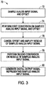
- FIG. 3 is a flowchart of an example of a method 70 of canceling an offset of a signal conditioning circuit coupled to an input of a multi-stage analog-to-digital converter (ADC) circuit using various techniques of this disclosure.
- the method 70 can include sampling an analog input signal and the offset.
- the control circuit 28 of FIG. 1A can close the switch S1 and the first S/H circuit 14 can sample the analog input signal V IN and the offset voltage V OFF of the signal conditioning circuit 12.
- the method 70 can include performing, by a first stage of the ADC circuit, a first conversion on the sampled analog input signal and offset V OFF .
- the control circuit 28 of FIG. 1B can open the switch S1 and close the switch S2 to couple the input of the signal conditioning circuit 12 to ground (if single-ended) to establish the offset V OFF of the signal conditioning circuit 12.
- the first stage of the multi-stage ADC circuit 10 can perform a conversion, e.g., coarse conversion, on the combination of the sampled analog input signal V IN and the offset voltage V OFF associated with that sample.
- the method 70 can include canceling the offset and amplifying a residue of the sampled analog input signal.
- the offset voltage V OFF can be canceled by subtracting the offset voltage V OFF (from coupling the input of the signal conditioning circuit 12 to ground) from the sum of the sampled analog input signal V IN and the offset voltage V OFF .
- the residue amplifier 20 can amplify the residue of the sampled analog input signal V IN .
- the method 70 can include performing, by a second stage of the ADC circuit, a second conversion on the residue of the sampled analog input signal.
- the second stage of the multi-stage ADC circuit 10 of FIG. ID can perform a conversion, e.g., a fine conversion, on the residue of the sampled analog input signal V IN (and generate a second stage output, or conversion result).
- the method 70 can include generating a digital output signal representing the sampled analog input signal.
- the encoder circuit 26 of FIG. ID can receive the first stage output (first stage conversion result) and the second stage output (second stage conversion result) and generate a digital output D OUT that represents the sampled analog input signal V IN .
- the speed of the multi-stage ADC circuit can be improved because the time for the residue amplifier to amplify and the time for the signal conditioning circuit to settle happen concurrently rather than sequentially (as in other approaches).
- the net time is the time of the residue amplifier to amplify.
- Method examples described herein may be machine or computer-implemented at least in part. Some examples may include a computer-readable medium or machine-readable medium encoded with instructions operable to configure an electronic device to perform methods as described in the above examples.
- An implementation of such methods may include code, such as microcode, assembly language code, a higher-level language code, or the like. Such code may include computer readable instructions for performing various methods. The code may form portions of computer program products. Further, in an example, the code may be tangibly stored on one or more volatile, non-transitory, or nonvolatile tangible computer-readable media, such as during execution or at other times.
- tangible computer-readable media may include, but are not limited to, hard disks, removable magnetic disks, removable optical disks (e.g., compact discs and digital video discs), magnetic cassettes, memory cards or sticks, random access memories (RAMs), read only memories (ROMs), and the like.
Landscapes
- Engineering & Computer Science (AREA)
- Theoretical Computer Science (AREA)
- Analogue/Digital Conversion (AREA)
Abstract
Description
- This document pertains generally to analog-to-digital converters.
- In many electronics applications, an analog input signal is converted to a digital output signal (e.g., for further digital signal processing). For instance, in precision measurement systems, electronics are provided with one or more sensors to make measurements, and these sensors can generate an analog signal. The analog signal can then be provided to an analog-to-digital converter (ADC) circuit as input to generate a digital output signal for further processing. In another instance, in a mobile device receiver, an antenna can generate an analog signal based on the electromagnetic waves carrying information/signals in the air. The analog signal generated by the antenna can then be provided as input to an ADC to generate a digital output signal for further processing.
- This disclosure is directed to, among other things, techniques to reduce the on-time of a multi-stage ADC circuit by combining the settling time of a signal conditioning circuit, e.g., buffer circuit, and the setting time of a residue amplifier when cancelling the offset of the signal conditioning circuit. The techniques of this disclosure can allow the signal conditioning circuit and the residue amplifier to settle together.
- In some aspects, this disclosure is directed to a method of canceling an offset of a signal conditioning circuit coupled to an input of a multi-stage analog-to-digital converter (ADC) circuit. The method comprises sampling an analog input signal and the offset; performing, by a first stage of the ADC circuit, a first conversion on the sampled analog input signal and offset; canceling the offset and amplifying a residue of the sampled analog input signal; performing, by a second stage of the ADC circuit, a second conversion on the residue of the sampled analog input signal; and generating a digital output signal representing the sampled analog input signal.
- In some aspects, this disclosure is directed to a multi-stage analog-to-digital converter (ADC) circuit having an input coupled to a signal conditioning circuit having an offset. The ADC circuit comprises a sample-and-hold circuit configured to sample an analog input signal and the offset; a first stage including a first ADC sub-circuit configured to perform a first conversion on the sampled analog input signal and offset; a control circuit configured to operate a plurality of switches to generate the residue of the first conversion and eliminate the signal conditioning circuit offset from the residue; a residue amplifier configured to amplify a residue of the sampled analog input signal; a second stage including a second ADC sub-circuit configured to perform a second conversion on the residue of the sampled analog input signal; and an encoder circuit configured to combine first and second conversion results and generate a digital output signal representing the sampled analog input signal.
- In some aspects, this disclosure is directed to a multi-stage analog-to-digital converter (ADC) circuit having an input coupled to a signal conditioning circuit having an offset. The ADC circuit comprises a sample-and-hold circuit configured to sample an analog input signal and the offset; means for performing, by a first stage of the ADC circuit, a first conversion on the sampled analog input signal and offset; means for canceling the offset and amplifying a residue of the sampled analog input signal; means for performing, by a second stage of the ADC circuit, a second conversion on the residue of the sampled analog input signal; and means for generating a digital output signal representing the sampled analog input signal.
- This overview is intended to provide an overview of subject matter of the present patent application. It is not intended to provide an exclusive or exhaustive explanation of the invention. The detailed description is included to provide further information about the present patent application.
- In the drawings, which are not necessarily drawn to scale, like numerals may describe similar components in different views. Like numerals having different letter suffixes may represent different instances of similar components. The drawings illustrate generally, by way of example, but not by way of limitation, various embodiments discussed in the present document.
-
FIG. 1A is a conceptual block diagram of an example of a multi-stage ADC circuit during a first phase of an operation that can implement various techniques of this disclosure. -
FIG. 1B is a conceptual block diagram of the multi-stage ADC circuit ofFIG. 1A during a second phase of operation. -
FIG. 1C is a conceptual block diagram of the multi-stage ADC circuit ofFIG. 1A during a third phase of operation. - FIG. ID is a conceptual block diagram of the multi-stage ADC circuit of
FIG. 1A during a fourth phase of operation. -
FIG. 2 is a conceptual block diagram of another example of a multi-stage ADC circuit that can implement various techniques of this disclosure. -
FIG. 3 is a flowchart of an example of a method of canceling an offset of a signal conditioning circuit coupled to an input of a multi-stage analog-to-digital converter (ADC) circuit using various techniques of this disclosure - Multi-stage analog-to-digital converters can utilize a successive series of stages (or cycles of operation) each arranged to develop a digital output of limited scope, e.g., one or more bits, and to produce from each stage (or cycle of operation) an analog residue signal as the input for the next stage (or cycle). In this way, a high-resolution output can be developed by combining the digital outputs of the several stages or cycles.
- Multi-stage ADC architectures can use inter-stage amplification, e.g., using a residue amplifier, particularly when the overall resolution exceeds about nine bits. Such amplification is for the purpose of raising the residue of one conversion to a level that can be digitized by the next subsequent stage.
- Multi-stage ADC architectures can use various analog-to-digital converter (ADC) topologies, including delta-sigma, flash, and successive approximation register (SAR) data converters. One of the attractive characteristics of SAR data converters is their ability to scale power consumption with conversion rate. The data converter only requires power during a conversion and can be powered down between conversions. Hence, the shorter the duty cycle the converter is on, the less power is consumed.
- Zero-drive data converters, e.g., converters that do not draw current from the input, can incorporate a buffer amplifier at the input, such that they can be driven by sources with a high impedance. Zero-drive converters can include buffer circuits, e.g., buffer amplifiers, or other signal conditioning circuitry, e.g., instrumentation amplifiers, transimpedance amplifiers, and filters, coupled to their inputs. To eliminate offset and 1/f noise generated by the signal conditioning circuitry, it can be chopped or auto-zeroed, for example. Both chopping and auto-zeroing can extend the time that the data-converter is powered up, and hence increase the duty cycle.
- In an existing approach to offset cancellation in a multi-stage ADC circuit, the offset of the signal conditioning circuit, e.g., buffer circuit, coupled to an input of the multi-stage ADC circuit can be auto-zeroed. Then, the analog input signal can be sampled.
- The first stage of the multi-stage ADC circuit can perform a coarse conversion on the sampled analog input signal to generate an output, e.g., the most significant bits (MSBs) and a residue signal. The residue signal is the difference between a feedback DAC output, which converts the coarse conversion output (MSBs) to an analog signal, and the sampled analog input signal. The residue signal can be amplified by a residue amplifier and transferred to the second stage of the multi-stage ADC circuit and the second stage can perform a fine conversion on the amplified residue signal to generate the remaining bits, e.g., the least significant bits (LSBs).
- In the case of chopping, the two sampling phases can include the sum of two half samples, each with an opposite polarity of the offset of the signal conditioning circuit. As such, the total conversion time would be similar to the approach described above.
- For a continuous running ADC, the signal conditioning circuit can perform auto-zeroing during one conversion (while the ADC is performing either a coarse conversion or a fine conversion, for example), and next apply the auto-zeroed signal conditioning circuit during the sampling phase of the next conversion. Hence, the algorithm can measure offset in one conversion, and correct for it in the next conversion. The offset therefore should be substantially constant between any two subsequent samples. Due to drift and 1/f noise, this condition fails when the time between two subsequent samples is too long, like in the case of convert on demand. In that case, the offset should be measured and eliminated within a conversion.
- The present inventors have recognized a need to eliminate the extra time needed for offset cancellation in a multi-stage ADC circuit. Using various techniques of this disclosure, the on-time of the multi-stage ADC circuit can be reduced by combining the settling time of a signal conditioning circuit, e.g., buffer circuit, and the setting time of a residue amplifier when cancelling the offset of the signal conditioning circuit. As described in detail below, the techniques of this disclosure can allow the signal conditioning circuit and the residue amplifier to settle together.
-
FIG. 1A is a conceptual block diagram of an example of amulti-stage ADC circuit 10 during a first phase of an operation that can implement various techniques of this disclosure. Asignal conditioning circuit 12, e.g., buffer circuit, having an offset voltage VOFF is coupled to an input of themulti-stage ADC circuit 10 and is configured to receive and condition an analog input signal VIN. Themulti-stage ADC circuit 10 shown inFIG. 1A can include two stages. The first stage can include a first sample-and-hold circuit (S/H) 14, afirst ADC sub-circuit 16, a first digital-to-analog converter (DAC)circuit 18, and aresidue amplifier circuit 20. The second stage can include a second S/H circuit 22, asecond ADC sub-circuit 24, and anencoder circuit 26. Acontrol circuit 28 can control various operations ofADC circuit 10, including closing and opening switches S1-S5. Thecontrol circuit 28 can operate the switches S1-S5 to generate or establish a residue of the first conversion and eliminate, e.g., concurrently, the signal conditioning circuit offset from that residue. - Operation of the
multi-stage ADC circuit 10 will now be briefly described, without specific reference to the first phase of operation. The first ADC sub-circuit 16 of the first stage can perform a first conversion, e.g., coarse conversion, on the sampled analog input signal to generate an output, e.g., the MSBs. A residue signal can be generated by subtracting the output of thefirst DAC circuit 18 from the sampled analog input signal VIN. The residue signal can be amplified by theresidue amplifier 20 and transferred to the second S/H circuit 22 of the second stage of themulti-stage ADC circuit 10. The second ADC sub-circuit 24 of the second stage can perform a second conversion, e.g., fine conversion, on the amplified residue signal to generate an output containing the remaining bits, e.g., the LSBs. Theencoder circuit 26 can receive the output of the first ADC sub-circuit 16 (a first conversion result) and the output of the second ADC sub-circuit 24 (a second conversion result) and generate a digital output signal DOUT. - During the first phase of operation, a
control circuit 28 can close the switches S1 and S4, open the switches S2, S3, and S5, and the first S/H circuit 14, e.g., including one or more capacitors, can sample the analog input signal VIN. The offset voltage VOFF of thesignal conditioning circuit 12 is added to the analog input signal VIN and sampled. During sampling, the remaining circuitry of themulti-stage ADC circuit 10 can be inactive and, as such, consuming little to no power. -
FIG. 1B is a conceptual block diagram of the multi-stage ADC circuit ofFIG. 1A during a second phase of operation. During the second phase of operation, thecontrol circuit 28 can open the switch S1 and close the switch S2 to couple the input of thesignal conditioning circuit 12 to ground (if single-ended) to establish the offset VOFF of thesignal conditioning circuit 12, and close the switch S5 to couple the first S/H circuit 14 to thefirst ADC sub-circuit 16. The first stage of themulti-stage ADC circuit 10 can perform a conversion, e.g., coarse conversion, on the combination of the sampled analog input signal VIN and the offset voltage VOFF associated with that sample and generate a first stage output. During this phase, one or more of thesignal conditioning circuit 12, theresidue amplifier 20, the second S/H circuit 22, thesecond ADC sub-circuit 24, and theencoder circuit 26 can be inactive and, as such, consume little to no power. -
FIG. 1C is a conceptual block diagram of the multi-stage ADC circuit ofFIG. 1A during a third phase of operation. During this phase, thesignal conditioning circuit 12, the first S/H circuit 14, thefirst DAC circuit 18, theresidue amplifier 20, and the second S/H circuit 22 can be active, and thefirst ADC sub-circuit 16, thesecond ADC sub-circuit 24, and theencoder circuit 26 can be inactive. During the third phase of operation, thecontrol circuit 28 can close the switch S3 to apply the offset voltage VOFF to the summingnode 15. The offset voltage VOFF can be canceled by subtracting the offset voltage VOFF (from coupling the input of thesignal conditioning circuit 12 to ground) from the sum of the sampled analog input signal VIN and the offset voltage VOFF. For example, the summingnode 15 can be configured to invert the offset input and the inverted offset voltage VOFF can be combined with the sum of the sampled analog input signal VIN and the offset voltage VOFF. Then, theresidue amplifier 20 can amplify the residue of the sampled analog input signal VIN. - In this manner, the offset voltage VOFF can be canceled while the
multi-stage ADC circuit 10 performs the residue amplification. Theresidue amplifier 20 takes time to amplify and the signal conditioning circuit takes time to settle. However, using the techniques described in this disclosure, the speed of the multi-stage ADC circuit can be improved because the time for the residue amplifier to amplify and the time for the signal conditioning circuit to settle happen concurrently rather than sequentially (as in other approaches). As such, the net time is the time of the residue amplifier to amplify. - FIG. ID is a conceptual block diagram of the multi-stage ADC circuit of
FIG. 1A during a fourth phase of operation. During this phase, the second S/H circuit 22 and the second ADC sub-circuit 24 can be active while the other circuitry can be powered off. During the fourth stage of operation, thecontrol circuit 28 can open the switch S3 and the second stage of themulti-stage ADC circuit 10 can perform a conversion, e.g., a fine conversion, on the residue of the sampled analog input signal VIN (and generate a second stage output). Theencoder circuit 26 can receive the first stage output and the second stage output and generate a digital output DOUT that represents the sampled analog input signal VIN. It should be noted that in some implementations, the second ADC sub-circuit 24 can be configured to accommodate an extra correction range for the offset that was added during the first stage of operation. - Although
FIGS. 1A-1D were described with respect to a two-stage ADC circuit, the techniques of this disclosure are applicable to multi-stage ADC circuits having more than two stages. In multi-stage converters, there can be a second, a third, and more stages. There can be a second residue amplifier, that amplifies the second residue from the second stage. And a third ADC sub-circuit can perform a third conversion on the residue from the second stage. An encoder combines the outputs of all ADC sub-circuits stages and generates the digital output. - The first ADC sub-circuit 16 of the first stage can be implemented using various ADC circuit topologies. For example, the
first ADC sub-circuit 16 can be a SAR ADC circuit configured to perform a conversion using a SAR algorithm. In other example implementations, thefirst ADC sub-circuit 16 can be a delta-sigma ADC circuit configured to perform a conversion using a delta-sigma algorithm. In other example implementations, thefirst ADC sub-circuit 16 can be a flash converter. - Similarly, the second ADC sub-circuit 24 of the second stage can be implemented using various ADC circuit topologies. For example, the second ADC sub-circuit 24 can be a SAR ADC circuit configured to perform a conversion using a SAR algorithm. In other example implementations, the second ADC sub-circuit 24 can be a delta-sigma ADC circuit configured to perform a conversion using a delta-sigma algorithm. In other example implementations, the second ADC sub-circuit 24 can be a flash converter.
- In other example configurations, the
first ADC sub-circuit 16 can be a hybrid ADC circuit configured to perform at least two algorithms selected from a group consisting of a successive approximation register (SAR) algorithm, a delta-sigma algorithm, and a flash algorithm. For example, thefirst ADC sub-circuit 16 can include both flash converter circuitry and SAR circuitry. Alternatively, or additionally, the second ADC sub-circuit can be configured as a hybrid ADC circuit. -
FIG. 2 depicts a specific non-limiting multi-stage ADC circuit that can implement various techniques in this disclosure. In particular, the multi-stage ADC circuit ofFIG. 2 utilizes SAR ADC sub-circuits. -
FIG. 2 is a conceptual block diagram of another example of a multi-stage ADC circuit that can implement various techniques of this disclosure. Themulti-stage ADC circuit 50 shown inFIG. 2 includes two stages, but the techniques are applicable to more than two stages. Themulti-stage ADC circuit 50 ofFIG. 2 can include components similar to those shown inFIGS. 1A-1D and are depicted with similar reference numbers. - The first stage can include a first sample-and-hold circuit (S/H) 14, a first SAR ADC sub-circuit including a
first comparator circuit 52 and a firstSAR register circuit 54, afirst DAC circuit 18, and aresidue amplifier circuit 20. The second stage can include a second S/H circuit 22, a second SAR ADC sub-circuit including asecond comparator circuit 56 and a secondSAR register circuit 58, and anencoder circuit 26. Abuffer circuit 60, having an offset voltage VOFF and coupled to an input of themulti-stage ADC circuit 50, is configured to receive and buffer an analog input signal VIN. - The
multi-stage ADC circuit 50 shown inFIG. 2 can operate in several phases, such as described above with respect toFIGS. 1A-1D . In general, the phases can include sampling the analog input signal VIN without auto-zeroing thebuffer circuit 60, performing a first conversion, e.g., coarse conversion, using the first SAR ADC sub-circuit, performing residue amplification of the sampled residue while cancelling the buffer offset, and performing a second conversion, e.g., fine conversion, using the second SAR ADC sub-circuit. -
FIG. 3 is a flowchart of an example of amethod 70 of canceling an offset of a signal conditioning circuit coupled to an input of a multi-stage analog-to-digital converter (ADC) circuit using various techniques of this disclosure. Atblock 72, themethod 70 can include sampling an analog input signal and the offset. For example, thecontrol circuit 28 ofFIG. 1A can close the switch S1 and the first S/H circuit 14 can sample the analog input signal VIN and the offset voltage VOFF of thesignal conditioning circuit 12. - At
block 74, themethod 70 can include performing, by a first stage of the ADC circuit, a first conversion on the sampled analog input signal and offset VOFF. For example, thecontrol circuit 28 ofFIG. 1B can open the switch S1 and close the switch S2 to couple the input of thesignal conditioning circuit 12 to ground (if single-ended) to establish the offset VOFF of thesignal conditioning circuit 12. The first stage of themulti-stage ADC circuit 10 can perform a conversion, e.g., coarse conversion, on the combination of the sampled analog input signal VIN and the offset voltage VOFF associated with that sample. - At
block 76, themethod 70 can include canceling the offset and amplifying a residue of the sampled analog input signal. For example, the offset voltage VOFF can be canceled by subtracting the offset voltage VOFF (from coupling the input of thesignal conditioning circuit 12 to ground) from the sum of the sampled analog input signal VIN and the offset voltage VOFF. Then, theresidue amplifier 20 can amplify the residue of the sampled analog input signal VIN. - At
block 78, themethod 70 can include performing, by a second stage of the ADC circuit, a second conversion on the residue of the sampled analog input signal. For example, the second stage of themulti-stage ADC circuit 10 of FIG. ID can perform a conversion, e.g., a fine conversion, on the residue of the sampled analog input signal VIN (and generate a second stage output, or conversion result). - At
block 80, themethod 70 can include generating a digital output signal representing the sampled analog input signal. For example, theencoder circuit 26 of FIG. ID can receive the first stage output (first stage conversion result) and the second stage output (second stage conversion result) and generate a digital output DOUT that represents the sampled analog input signal VIN. - Using the techniques described above, the speed of the multi-stage ADC circuit can be improved because the time for the residue amplifier to amplify and the time for the signal conditioning circuit to settle happen concurrently rather than sequentially (as in other approaches). Thus, the net time is the time of the residue amplifier to amplify.
- Each of the non-limiting aspects or examples described herein may stand on its own or may be combined in various permutations or combinations with one or more of the other examples.
- The above detailed description includes references to the accompanying drawings, which form a part of the detailed description. The drawings show, by way of illustration, specific embodiments in which the invention may be practiced. These embodiments are also referred to herein as "examples." Such examples may include elements in addition to those shown or described. However, the present inventors also contemplate examples in which only those elements shown or described are provided. Moreover, the present inventors also contemplate examples using any combination or permutation of those elements shown or described (or one or more aspects thereof), either with respect to a particular example (or one or more aspects thereof), or with respect to other examples (or one or more aspects thereof) shown or described herein.
- In the event of inconsistent usages between this document and any documents so incorporated by reference, the usage in this document controls.
- In this document, the terms "a" or "an" are used, as is common in patent documents, to include one or more than one, independent of any other instances or usages of "at least one" or "one or more." In this document, the term "or" is used to refer to a nonexclusive or, such that "A or B" includes "A but not B," "B but not A," and "A and B," unless otherwise indicated. In this document, the terms "including" and "in which" are used as the plain-English equivalents of the respective terms "comprising" and "wherein." Also, in the following claims, the terms "including" and "comprising" are open-ended, that is, a system, device, article, composition, formulation, or process that includes elements in addition to those listed after such a term in a claim are still deemed to fall within the scope of that claim. Moreover, in the following claims, the terms "first," "second," and "third," etc. are used merely as labels, and are not intended to impose numerical requirements on their objects.
- Method examples described herein may be machine or computer-implemented at least in part. Some examples may include a computer-readable medium or machine-readable medium encoded with instructions operable to configure an electronic device to perform methods as described in the above examples. An implementation of such methods may include code, such as microcode, assembly language code, a higher-level language code, or the like. Such code may include computer readable instructions for performing various methods. The code may form portions of computer program products. Further, in an example, the code may be tangibly stored on one or more volatile, non-transitory, or nonvolatile tangible computer-readable media, such as during execution or at other times. Examples of these tangible computer-readable media may include, but are not limited to, hard disks, removable magnetic disks, removable optical disks (e.g., compact discs and digital video discs), magnetic cassettes, memory cards or sticks, random access memories (RAMs), read only memories (ROMs), and the like.
- The above description is intended to be illustrative, and not restrictive. For example, the above-described examples (or one or more aspects thereof) may be used in combination with each other. Other embodiments may be used, such as by one of ordinary skill in the art upon reviewing the above description. The Abstract is provided to comply with 37 C.F.R. § 1.72(b), to allow the reader to quickly ascertain the nature of the technical disclosure. It is submitted with the understanding that it will not be used to interpret or limit the scope or meaning of the claims. Also, in the above Detailed Description, various features may be grouped together to streamline the disclosure. This should not be interpreted as intending that an unclaimed disclosed feature is essential to any claim. Rather, inventive subject matter may lie in less than all features of a particular disclosed embodiment. Thus, the following claims are hereby incorporated into the Detailed Description as examples or embodiments, with each claim standing on its own as a separate embodiment, and it is contemplated that such embodiments may be combined with each other in various combinations or permutations. The scope of the invention should be determined with reference to the appended claims, along with the full scope of equivalents to which such claims are entitled.
Claims (15)
- A method of canceling an offset of a signal conditioning circuit coupled to an input of a multi-stage analog-to-digital converter (ADC) circuit, the method comprising:sampling an analog input signal and the offset;performing, by a first stage of the ADC circuit, a first conversion on the sampled analog input signal and offset;canceling the offset and amplifying a residue of the sampled analog input signal;performing, by a second stage of the ADC circuit, a second conversion on the residue of the sampled analog input signal; andgenerating a digital output signal representing the sampled analog input signal.
- The method of claim 1, wherein canceling the offset comprises:shorting an input of the signal conditioning circuit to determine the offset; andsubtracting the offset from the sampled analog input signal and offset.
- The method of any preceding claim, wherein performing, by the first stage of the ADC circuit, the first conversion on the sampled analog input signal and offset includes:
performing, by the first stage of the ADC circuit, the first conversion on the sampled analog input signal and offset using a successive approximation register (SAR) algorithm. - The method of any preceding claim, wherein performing, by the first stage of the ADC circuit, the first conversion on the sampled analog input signal and offset includes:
performing, by the first stage of the ADC circuit, the first conversion on the sampled analog input signal and offset using a delta-sigma algorithm. - The method of any preceding claim, wherein performing, by the first stage of the ADC circuit, the first conversion on the sampled analog input signal and offset includes:
performing, by the first stage of the ADC circuit, the first conversion on the sampled analog input signal and offset using a flash converter. - The method of any preceding claim, wherein performing, by the second stage of the ADC circuit, the second conversion on the residue of the sampled analog input includes:
performing, by the second stage of the ADC circuit, the second conversion on the residue of the sampled analog input using a successive approximation register (SAR) algorithm. - The method of any preceding claim, wherein performing, by the second stage of the ADC circuit, the second conversion on the residue of the sampled analog input includes:
performing, by the second stage of the ADC circuit, the second conversion on the residue of the sampled analog input using a delta-sigma algorithm. - The method of any preceding claim, wherein performing, by the second stage of the ADC circuit, the second conversion on the residue of the sampled analog input includes:
performing, by the second stage of the ADC circuit, the second conversion on the residue of the sampled analog input using a flash converter. - A multi-stage analog-to-digital converter (ADC) circuit having an input coupled to a signal conditioning circuit having an offset, the ADC circuit comprising:a sample-and-hold circuit configured to sample an analog input signal and the offset;a first stage including a first ADC sub-circuit configured to perform a first conversion on the sampled analog input signal and offset;a control circuit configured to operate a plurality of switches to generate the residue of the first conversion and eliminate the signal conditioning circuit offset from the residue;a residue amplifier configured to amplify the residue of the sampled analog input signal;a second stage including a second ADC sub-circuit configured to perform a second conversion on the residue of the sampled analog input signal; andan encoder circuit configured to combine first and second conversion results and generate a digital output signal representing the sampled analog input signal.
- The circuit of claim 9, wherein the first ADC sub-circuit includes at least one of:a successive approximation register (SAR) ADC configured to perform a SAR algorithm;a delta-sigma ADC configured to perform a delta-sigma algorithm;a flash ADC configured to perform a flash algorithm.
- The circuit of claim 9 or claim 10, wherein the second ADC sub-circuit includes at least one of:a successive approximation register (SAR) ADC configured to perform a SAR algorithm;a delta-sigma ADC configured to perform a delta-sigma algorithm;a flash ADC configured to perform a flash algorithm.
- The circuit of any of claims 9 to 11, wherein the first ADC sub-circuit and/or the second ADC sub-circuit is a hybrid ADC circuit configured to perform at least two algorithms selected from a group consisting of a successive approximation register (SAR) algorithm, a delta-sigma algorithm, and a flash algorithm.
- The circuit of any of claims 9 to 12, wherein the signal conditioning circuit is a buffer circuit.
- A multi-stage analog-to-digital converter (ADC) circuit having an input coupled to a signal conditioning circuit having an offset, the ADC circuit comprising:a sample-and-hold circuit configured to sample an analog input signal and the offset;means for performing, by a first stage of the ADC circuit, a first conversion on the sampled analog input signal and offset;means for canceling the offset and amplifying a residue of the sampled analog input signal;means for performing, by a second stage of the ADC circuit, a second conversion on the residue of the sampled analog input signal; andmeans for generating a digital output signal representing the sampled analog input signal.
- The circuit of claim 14, wherein at least one of the following applies:a) the means for performing, by the first stage of the ADC circuit, the first conversion on the sampled analog input signal and offset includes a successive approximation register (SAR) ADC configured to perform a SAR algorithm;b) the means for performing, by the second stage of the ADC circuit, the second conversion on the residue of the sampled analog input signal includes a successive approximation register (SAR) ADC configured to perform a SAR algorithm.
Applications Claiming Priority (1)
| Application Number | Priority Date | Filing Date | Title |
|---|---|---|---|
| US16/706,230 US10868554B1 (en) | 2019-12-06 | 2019-12-06 | Time-efficient offset cancellation for multi-stage converters |
Publications (2)
| Publication Number | Publication Date |
|---|---|
| EP3832889A1 true EP3832889A1 (en) | 2021-06-09 |
| EP3832889B1 EP3832889B1 (en) | 2025-04-09 |
Family
ID=73646167
Family Applications (1)
| Application Number | Title | Priority Date | Filing Date |
|---|---|---|---|
| EP20210620.9A Active EP3832889B1 (en) | 2019-12-06 | 2020-11-30 | Time-efficient offset cancellation for multi-stage converters |
Country Status (5)
| Country | Link |
|---|---|
| US (1) | US10868554B1 (en) |
| EP (1) | EP3832889B1 (en) |
| JP (1) | JP7157125B2 (en) |
| CN (1) | CN112929027B (en) |
| TW (1) | TWI755179B (en) |
Families Citing this family (4)
| Publication number | Priority date | Publication date | Assignee | Title |
|---|---|---|---|---|
| US10979064B2 (en) * | 2018-10-31 | 2021-04-13 | Taiwan Semiconductor Manufacturing Company, Ltd. | Analog to digital converter with inverter based amplifier |
| US12494791B2 (en) * | 2021-06-25 | 2025-12-09 | Intel Corporation | Analog-to-digital converter system, receiver, base station, mobile device and method for analog-to-digital conversion |
| JP2024153345A (en) | 2023-04-17 | 2024-10-29 | キヤノン株式会社 | AD conversion circuit, photoelectric conversion device, photoelectric conversion system, mobile object |
| US20250183905A1 (en) * | 2023-12-05 | 2025-06-05 | Arctic Semiconductor Corporation | Multi-stage pipeline sar analog-to-digital converter (adc) |
Family Cites Families (37)
| Publication number | Priority date | Publication date | Assignee | Title |
|---|---|---|---|---|
| JP3701037B2 (en) * | 1994-01-11 | 2005-09-28 | 富士通株式会社 | Sample and hold circuit |
| US6289070B1 (en) | 1997-04-22 | 2001-09-11 | Silicon Laboratories, Inc. | Digital isolation system with ADC offset calibration including coarse offset |
| US6285309B1 (en) | 1999-09-14 | 2001-09-04 | Texas Instruments Incorporated | Nested pipelined analog-to-digital converter |
| US6323791B1 (en) | 1999-10-13 | 2001-11-27 | Analog Devices, Inc. | Control systems and methods for reducing residue signal offset in subranging analog-to-digital converters |
| US6396429B2 (en) * | 2000-01-07 | 2002-05-28 | Analog Devices, Inc. | Front-end sampling for analog-to-digital conversion |
| US6608575B2 (en) | 2001-01-31 | 2003-08-19 | Qualcomm Incorporated | Hybrid multi-stage circuit |
| US6617992B2 (en) * | 2001-08-15 | 2003-09-09 | National Semiconductor Corporation | Capacitor mismatch independent gain stage for differential pipeline analog to digital converters |
| JP3971414B2 (en) * | 2004-07-16 | 2007-09-05 | ローム株式会社 | A / D conversion device and communication device using the same |
| US7339512B2 (en) * | 2004-09-17 | 2008-03-04 | Edgewater Computer Systems, Inc. | Analog-to-digital converter without track-and-hold |
| JP4893896B2 (en) * | 2006-06-08 | 2012-03-07 | 国立大学法人静岡大学 | Analog-digital converter, A / D conversion stage, method for generating digital signal corresponding to analog signal, and method for generating signal indicating conversion error in A / D conversion stage |
| US7538701B2 (en) * | 2006-06-08 | 2009-05-26 | Cosmic Circuits Private Limited | System and method for improving dynamic performance of a circuit |
| JP4480744B2 (en) * | 2007-07-31 | 2010-06-16 | 三洋電機株式会社 | Analog to digital converter |
| KR20100073009A (en) | 2008-12-22 | 2010-07-01 | 한국전자통신연구원 | Multi-stage dual successive approximation register analog-digtal converter and analog-digtal converting method theerof |
| US7978115B2 (en) * | 2009-07-06 | 2011-07-12 | Raytheon Company | System and method for analog-to-digital conversion |
| US7999710B2 (en) * | 2009-09-15 | 2011-08-16 | Texas Instruments Incorporated | Multistage chopper stabilized delta-sigma ADC with reduced offset |
| US8018370B2 (en) * | 2010-02-01 | 2011-09-13 | Linear Technology Corporation | Time-multiplexed residue amplifier |
| US8284090B2 (en) | 2010-03-22 | 2012-10-09 | Analog Devices, Inc. | Method and apparatus for analog to digital conversion of small signals in the presence of a large DC offset |
| EP2629428A1 (en) | 2012-02-16 | 2013-08-21 | Imec | A/D Converter and Method for Calibrating the Same |
| US8723706B1 (en) | 2012-08-28 | 2014-05-13 | Maxim Integrated Products, Inc. | Multi-step ADC with sub-ADC calibration |
| US8659461B1 (en) | 2012-11-13 | 2014-02-25 | University Of Macau | Analog to digital converter circuit |
| US8779963B1 (en) * | 2013-03-12 | 2014-07-15 | Maxin Integrated Products, Inc. | Reconfigurable multiple-path pipeline ADC architecture incorporating multiple-input signal-averaging MDAC |
| CN104426549B (en) | 2013-09-11 | 2020-02-28 | 马克西姆综合产品公司 | Multi-step ADC with sub-ADC calibration |
| US9178529B2 (en) * | 2013-10-18 | 2015-11-03 | Analog Devices Global | Multi-stage noise shaping analog-to-digital converter |
| US8884801B1 (en) | 2013-11-21 | 2014-11-11 | Inphi Corporation | High-speed analog-to-digital conversion system with flash assisted parallel SAR architecture |
| US9503119B2 (en) * | 2014-05-29 | 2016-11-22 | Texas Instruments Incorporated | Common mode sampling mechanism for residue amplifier in switched current pipeline analog-to-digital converters |
| US9154146B1 (en) * | 2014-06-03 | 2015-10-06 | The Board Of Regents, The University Of Texas System | Dynamic offset injection for CMOS ADC front-end linearization |
| EP3836403B1 (en) | 2014-12-17 | 2025-12-03 | Analog Devices, Inc. | Microprocessor-assisted calibration for analog-to-digital converter |
| US9525428B2 (en) * | 2014-12-17 | 2016-12-20 | Analog Devices, Inc. | Randomly sampling reference ADC for calibration |
| JP6469496B2 (en) * | 2015-03-31 | 2019-02-13 | ルネサスエレクトロニクス株式会社 | Semiconductor device and analog-digital conversion circuit calibration method |
| US9654132B2 (en) | 2015-07-08 | 2017-05-16 | Marvell World Trade Ltd. | Hybrid charge-sharing charge-redistribution DAC for successive approximation analog-to-digital converters |
| US9455737B1 (en) | 2015-09-25 | 2016-09-27 | Qualcomm Incorporated | Delta-sigma analog-to-digital converter (ADC) with time-interleaved (TI) or two-step successive approximation register (SAR) quantizer |
| US9571115B1 (en) | 2015-11-13 | 2017-02-14 | International Business Machines Corporation | Analog to digital converter with high precision offset calibrated integrating comparators |
| US10284145B2 (en) | 2016-11-03 | 2019-05-07 | Board Of Regents, The University Of Texas System | Variable gain amplifier utilizing positive feedback and time-domain calibration |
| EP3503407B1 (en) | 2017-12-19 | 2021-04-07 | IMEC vzw | Improvements in or related to analog-to-digital converters |
| US10128859B1 (en) * | 2018-02-20 | 2018-11-13 | Analog Devices Global Unlimited Company | Correlated double sampling analog-to-digital converter |
| US10868557B2 (en) * | 2018-03-30 | 2020-12-15 | Taiwan Semiconductor Manufacturing Company, Ltd | Analog to digital converter with current steering stage |
| US10608655B1 (en) * | 2018-12-06 | 2020-03-31 | Analog Devices, Inc. | Inter-stage gain calibration in double conversion analog-to-digital converter |
-
2019
- 2019-12-06 US US16/706,230 patent/US10868554B1/en active Active
-
2020
- 2020-11-30 EP EP20210620.9A patent/EP3832889B1/en active Active
- 2020-12-02 TW TW109142340A patent/TWI755179B/en active
- 2020-12-04 JP JP2020201819A patent/JP7157125B2/en active Active
- 2020-12-04 CN CN202011413878.XA patent/CN112929027B/en active Active
Non-Patent Citations (3)
| Title |
|---|
| BONGSUB SONG ET AL: "An Autofocus Sensor With Global Shutter Using Offset-Free Frame Memory", IEEE TRANSACTIONS ON CIRCUITS AND SYSTEMS II: EXPRESS BRIEFS, IEEE, US, vol. 57, no. 11, 1 November 2010 (2010-11-01), pages 878 - 882, XP011320196, ISSN: 1549-7747 * |
| GANESH RAAJA M ET AL: "Calibrating Amplifiers and ADCs in SoCs", 5 February 2012 (2012-02-05), pages 1 - 9, XP055797179, Retrieved from the Internet <URL:https://www.planetanalog.com/ContentEETimes/Documents/Schweber/C0941/C0941edited.pdf> [retrieved on 20210420], DOI: 10.1.1.370.6297 * |
| SEGUINE DENNIS: "AN2226 PSoC 1 -Using Correlated Double Sampling to Reduce Offset, Drift, and Low Frequency Noise", 22 April 2015 (2015-04-22), pages 1 - 11, XP055797182, Retrieved from the Internet <URL:https://www.cypress.com/file/126666/download> [retrieved on 20210420] * |
Also Published As
| Publication number | Publication date |
|---|---|
| EP3832889B1 (en) | 2025-04-09 |
| JP2021093725A (en) | 2021-06-17 |
| US10868554B1 (en) | 2020-12-15 |
| CN112929027B (en) | 2024-05-31 |
| CN112929027A (en) | 2021-06-08 |
| TWI755179B (en) | 2022-02-11 |
| TW202131640A (en) | 2021-08-16 |
| JP7157125B2 (en) | 2022-10-19 |
Similar Documents
| Publication | Publication Date | Title |
|---|---|---|
| EP3832889B1 (en) | Time-efficient offset cancellation for multi-stage converters | |
| US11190197B2 (en) | Correlated double sampling analog-to-digital converter | |
| US11545991B2 (en) | Analog-to-digital converter with auto-zeroing residue amplification circuit | |
| EP2629429B1 (en) | A/D converter and method for calibrating the same | |
| US7911370B2 (en) | Pipeline analog-to-digital converter with programmable gain function | |
| US7796077B2 (en) | High speed high resolution ADC using successive approximation technique | |
| US10355709B1 (en) | Multiplexed sigma-delta analog-to-digital converter | |
| EP3793092B1 (en) | Low noise analog-to-digital converter | |
| US10348319B1 (en) | Reservoir capacitor based analog-to-digital converter | |
| US8164497B2 (en) | Pipeline analog-to-digital converter | |
| US9077373B1 (en) | Analog-to-digital conversion apparatus | |
| US9019137B1 (en) | Multiplying digital-to-analog converter | |
| US7570191B2 (en) | Methods and systems for designing high resolution analog to digital converters | |
| EP2338229B1 (en) | Switched-capacitor pipeline stage | |
| KR100340073B1 (en) | Successive approximation register type analog-digital converter | |
| EP1105971A1 (en) | Floating-point analog-to-digital converter | |
| JP6739485B2 (en) | Analog-to-digital converter with noise reduction | |
| CN121643737B (en) | Thermal noise cancellation high-precision ADC and its implementation method | |
| KR102092635B1 (en) | Dynamic residue amplifier and the using pipelined analog-to-digital converter | |
| CN120956265A (en) | Error calibration methods, devices, equipment, and storage media for analog-to-digital converter (ADC) circuits. | |
| Marble | A 10-bit charge-transfer amplifier-based A/D converter with 400-µ W/MSPS dynamic power dissipation | |
| WO2010004456A1 (en) | Digital-to-analogue converter |
Legal Events
| Date | Code | Title | Description |
|---|---|---|---|
| PUAI | Public reference made under article 153(3) epc to a published international application that has entered the european phase |
Free format text: ORIGINAL CODE: 0009012 |
|
| STAA | Information on the status of an ep patent application or granted ep patent |
Free format text: STATUS: THE APPLICATION HAS BEEN PUBLISHED |
|
| AK | Designated contracting states |
Kind code of ref document: A1 Designated state(s): AL AT BE BG CH CY CZ DE DK EE ES FI FR GB GR HR HU IE IS IT LI LT LU LV MC MK MT NL NO PL PT RO RS SE SI SK SM TR |
|
| STAA | Information on the status of an ep patent application or granted ep patent |
Free format text: STATUS: REQUEST FOR EXAMINATION WAS MADE |
|
| 17P | Request for examination filed |
Effective date: 20211028 |
|
| RBV | Designated contracting states (corrected) |
Designated state(s): AL AT BE BG CH CY CZ DE DK EE ES FI FR GB GR HR HU IE IS IT LI LT LU LV MC MK MT NL NO PL PT RO RS SE SI SK SM TR |
|
| STAA | Information on the status of an ep patent application or granted ep patent |
Free format text: STATUS: EXAMINATION IS IN PROGRESS |
|
| 17Q | First examination report despatched |
Effective date: 20230504 |
|
| RIC1 | Information provided on ipc code assigned before grant |
Ipc: H03M 1/16 20060101ALN20241129BHEP Ipc: H03M 1/06 20060101AFI20241129BHEP |
|
| GRAP | Despatch of communication of intention to grant a patent |
Free format text: ORIGINAL CODE: EPIDOSNIGR1 |
|
| STAA | Information on the status of an ep patent application or granted ep patent |
Free format text: STATUS: GRANT OF PATENT IS INTENDED |
|
| RIC1 | Information provided on ipc code assigned before grant |
Ipc: H03M 1/16 20060101ALN20250113BHEP Ipc: H03M 1/06 20060101AFI20250113BHEP |
|
| GRAS | Grant fee paid |
Free format text: ORIGINAL CODE: EPIDOSNIGR3 |
|
| INTG | Intention to grant announced |
Effective date: 20250204 |
|
| RIC1 | Information provided on ipc code assigned before grant |
Ipc: H03M 1/16 20060101ALN20250127BHEP Ipc: H03M 1/06 20060101AFI20250127BHEP |
|
| GRAA | (expected) grant |
Free format text: ORIGINAL CODE: 0009210 |
|
| STAA | Information on the status of an ep patent application or granted ep patent |
Free format text: STATUS: THE PATENT HAS BEEN GRANTED |
|
| AK | Designated contracting states |
Kind code of ref document: B1 Designated state(s): AL AT BE BG CH CY CZ DE DK EE ES FI FR GB GR HR HU IE IS IT LI LT LU LV MC MK MT NL NO PL PT RO RS SE SI SK SM TR |
|
| REG | Reference to a national code |
Ref country code: GB Ref legal event code: FG4D |
|
| REG | Reference to a national code |
Ref country code: CH Ref legal event code: EP |
|
| REG | Reference to a national code |
Ref country code: DE Ref legal event code: R096 Ref document number: 602020049021 Country of ref document: DE |
|
| REG | Reference to a national code |
Ref country code: IE Ref legal event code: FG4D |
|
| REG | Reference to a national code |
Ref country code: NL Ref legal event code: MP Effective date: 20250409 |
|
| PG25 | Lapsed in a contracting state [announced via postgrant information from national office to epo] |
Ref country code: NL Free format text: LAPSE BECAUSE OF FAILURE TO SUBMIT A TRANSLATION OF THE DESCRIPTION OR TO PAY THE FEE WITHIN THE PRESCRIBED TIME-LIMIT Effective date: 20250409 |
|
| REG | Reference to a national code |
Ref country code: AT Ref legal event code: MK05 Ref document number: 1784483 Country of ref document: AT Kind code of ref document: T Effective date: 20250409 |
|
| PG25 | Lapsed in a contracting state [announced via postgrant information from national office to epo] |
Ref country code: PT Free format text: LAPSE BECAUSE OF FAILURE TO SUBMIT A TRANSLATION OF THE DESCRIPTION OR TO PAY THE FEE WITHIN THE PRESCRIBED TIME-LIMIT Effective date: 20250811 Ref country code: FI Free format text: LAPSE BECAUSE OF FAILURE TO SUBMIT A TRANSLATION OF THE DESCRIPTION OR TO PAY THE FEE WITHIN THE PRESCRIBED TIME-LIMIT Effective date: 20250409 Ref country code: ES Free format text: LAPSE BECAUSE OF FAILURE TO SUBMIT A TRANSLATION OF THE DESCRIPTION OR TO PAY THE FEE WITHIN THE PRESCRIBED TIME-LIMIT Effective date: 20250409 |
|
| REG | Reference to a national code |
Ref country code: LT Ref legal event code: MG9D |
|
| PG25 | Lapsed in a contracting state [announced via postgrant information from national office to epo] |
Ref country code: NO Free format text: LAPSE BECAUSE OF FAILURE TO SUBMIT A TRANSLATION OF THE DESCRIPTION OR TO PAY THE FEE WITHIN THE PRESCRIBED TIME-LIMIT Effective date: 20250709 Ref country code: GR Free format text: LAPSE BECAUSE OF FAILURE TO SUBMIT A TRANSLATION OF THE DESCRIPTION OR TO PAY THE FEE WITHIN THE PRESCRIBED TIME-LIMIT Effective date: 20250710 |
|
| PG25 | Lapsed in a contracting state [announced via postgrant information from national office to epo] |
Ref country code: PL Free format text: LAPSE BECAUSE OF FAILURE TO SUBMIT A TRANSLATION OF THE DESCRIPTION OR TO PAY THE FEE WITHIN THE PRESCRIBED TIME-LIMIT Effective date: 20250409 |
|
| PG25 | Lapsed in a contracting state [announced via postgrant information from national office to epo] |
Ref country code: BG Free format text: LAPSE BECAUSE OF FAILURE TO SUBMIT A TRANSLATION OF THE DESCRIPTION OR TO PAY THE FEE WITHIN THE PRESCRIBED TIME-LIMIT Effective date: 20250409 |
|
| PG25 | Lapsed in a contracting state [announced via postgrant information from national office to epo] |
Ref country code: HR Free format text: LAPSE BECAUSE OF FAILURE TO SUBMIT A TRANSLATION OF THE DESCRIPTION OR TO PAY THE FEE WITHIN THE PRESCRIBED TIME-LIMIT Effective date: 20250409 |
|
| PG25 | Lapsed in a contracting state [announced via postgrant information from national office to epo] |
Ref country code: AT Free format text: LAPSE BECAUSE OF FAILURE TO SUBMIT A TRANSLATION OF THE DESCRIPTION OR TO PAY THE FEE WITHIN THE PRESCRIBED TIME-LIMIT Effective date: 20250409 |
|
| PG25 | Lapsed in a contracting state [announced via postgrant information from national office to epo] |
Ref country code: RS Free format text: LAPSE BECAUSE OF FAILURE TO SUBMIT A TRANSLATION OF THE DESCRIPTION OR TO PAY THE FEE WITHIN THE PRESCRIBED TIME-LIMIT Effective date: 20250709 |
|
| PG25 | Lapsed in a contracting state [announced via postgrant information from national office to epo] |
Ref country code: IS Free format text: LAPSE BECAUSE OF FAILURE TO SUBMIT A TRANSLATION OF THE DESCRIPTION OR TO PAY THE FEE WITHIN THE PRESCRIBED TIME-LIMIT Effective date: 20250809 |
|
| PG25 | Lapsed in a contracting state [announced via postgrant information from national office to epo] |
Ref country code: LV Free format text: LAPSE BECAUSE OF FAILURE TO SUBMIT A TRANSLATION OF THE DESCRIPTION OR TO PAY THE FEE WITHIN THE PRESCRIBED TIME-LIMIT Effective date: 20250409 |
|
| PGFP | Annual fee paid to national office [announced via postgrant information from national office to epo] |
Ref country code: DE Payment date: 20251022 Year of fee payment: 6 |
|
| REG | Reference to a national code |
Ref country code: DE Ref legal event code: R097 Ref document number: 602020049021 Country of ref document: DE |
|
| PG25 | Lapsed in a contracting state [announced via postgrant information from national office to epo] |
Ref country code: DK Free format text: LAPSE BECAUSE OF FAILURE TO SUBMIT A TRANSLATION OF THE DESCRIPTION OR TO PAY THE FEE WITHIN THE PRESCRIBED TIME-LIMIT Effective date: 20250409 Ref country code: SM Free format text: LAPSE BECAUSE OF FAILURE TO SUBMIT A TRANSLATION OF THE DESCRIPTION OR TO PAY THE FEE WITHIN THE PRESCRIBED TIME-LIMIT Effective date: 20250409 |
|
| PG25 | Lapsed in a contracting state [announced via postgrant information from national office to epo] |
Ref country code: CZ Free format text: LAPSE BECAUSE OF FAILURE TO SUBMIT A TRANSLATION OF THE DESCRIPTION OR TO PAY THE FEE WITHIN THE PRESCRIBED TIME-LIMIT Effective date: 20250409 |
|
| PG25 | Lapsed in a contracting state [announced via postgrant information from national office to epo] |
Ref country code: EE Free format text: LAPSE BECAUSE OF FAILURE TO SUBMIT A TRANSLATION OF THE DESCRIPTION OR TO PAY THE FEE WITHIN THE PRESCRIBED TIME-LIMIT Effective date: 20250409 |
|
| PG25 | Lapsed in a contracting state [announced via postgrant information from national office to epo] |
Ref country code: SK Free format text: LAPSE BECAUSE OF FAILURE TO SUBMIT A TRANSLATION OF THE DESCRIPTION OR TO PAY THE FEE WITHIN THE PRESCRIBED TIME-LIMIT Effective date: 20250409 Ref country code: RO Free format text: LAPSE BECAUSE OF FAILURE TO SUBMIT A TRANSLATION OF THE DESCRIPTION OR TO PAY THE FEE WITHIN THE PRESCRIBED TIME-LIMIT Effective date: 20250409 |
|
| PG25 | Lapsed in a contracting state [announced via postgrant information from national office to epo] |
Ref country code: IT Free format text: LAPSE BECAUSE OF FAILURE TO SUBMIT A TRANSLATION OF THE DESCRIPTION OR TO PAY THE FEE WITHIN THE PRESCRIBED TIME-LIMIT Effective date: 20250409 |
|
| PLBE | No opposition filed within time limit |
Free format text: ORIGINAL CODE: 0009261 |
|
| STAA | Information on the status of an ep patent application or granted ep patent |
Free format text: STATUS: NO OPPOSITION FILED WITHIN TIME LIMIT |
|
| REG | Reference to a national code |
Ref country code: CH Ref legal event code: L10 Free format text: ST27 STATUS EVENT CODE: U-0-0-L10-L00 (AS PROVIDED BY THE NATIONAL OFFICE) Effective date: 20260218 |
|
| 26N | No opposition filed |
Effective date: 20260112 |