EP3832731A1 - Electroluminescent display device and method of manufacturing the same - Google Patents
Electroluminescent display device and method of manufacturing the same Download PDFInfo
- Publication number
- EP3832731A1 EP3832731A1 EP20211892.3A EP20211892A EP3832731A1 EP 3832731 A1 EP3832731 A1 EP 3832731A1 EP 20211892 A EP20211892 A EP 20211892A EP 3832731 A1 EP3832731 A1 EP 3832731A1
- Authority
- EP
- European Patent Office
- Prior art keywords
- layer
- electrode
- bank
- connection pattern
- light
- Prior art date
- Legal status (The legal status is an assumption and is not a legal conclusion. Google has not performed a legal analysis and makes no representation as to the accuracy of the status listed.)
- Granted
Links
Images



Classifications
-
- H—ELECTRICITY
- H10—SEMICONDUCTOR DEVICES; ELECTRIC SOLID-STATE DEVICES NOT OTHERWISE PROVIDED FOR
- H10K—ORGANIC ELECTRIC SOLID-STATE DEVICES
- H10K59/00—Integrated devices, or assemblies of multiple devices, comprising at least one organic light-emitting element covered by group H10K50/00
- H10K59/10—OLED displays
- H10K59/12—Active-matrix OLED [AMOLED] displays
- H10K59/123—Connection of the pixel electrodes to the thin film transistors [TFT]
-
- H—ELECTRICITY
- H10—SEMICONDUCTOR DEVICES; ELECTRIC SOLID-STATE DEVICES NOT OTHERWISE PROVIDED FOR
- H10K—ORGANIC ELECTRIC SOLID-STATE DEVICES
- H10K59/00—Integrated devices, or assemblies of multiple devices, comprising at least one organic light-emitting element covered by group H10K50/00
- H10K59/10—OLED displays
- H10K59/12—Active-matrix OLED [AMOLED] displays
- H10K59/131—Interconnections, e.g. wiring lines or terminals
- H10K59/1315—Interconnections, e.g. wiring lines or terminals comprising structures specially adapted for lowering the resistance
-
- H—ELECTRICITY
- H10—SEMICONDUCTOR DEVICES; ELECTRIC SOLID-STATE DEVICES NOT OTHERWISE PROVIDED FOR
- H10K—ORGANIC ELECTRIC SOLID-STATE DEVICES
- H10K50/00—Organic light-emitting devices
- H10K50/10—OLEDs or polymer light-emitting diodes [PLED]
- H10K50/11—OLEDs or polymer light-emitting diodes [PLED] characterised by the electroluminescent [EL] layers
-
- H—ELECTRICITY
- H10—SEMICONDUCTOR DEVICES; ELECTRIC SOLID-STATE DEVICES NOT OTHERWISE PROVIDED FOR
- H10K—ORGANIC ELECTRIC SOLID-STATE DEVICES
- H10K50/00—Organic light-emitting devices
- H10K50/80—Constructional details
- H10K50/805—Electrodes
-
- H—ELECTRICITY
- H10—SEMICONDUCTOR DEVICES; ELECTRIC SOLID-STATE DEVICES NOT OTHERWISE PROVIDED FOR
- H10K—ORGANIC ELECTRIC SOLID-STATE DEVICES
- H10K50/00—Organic light-emitting devices
- H10K50/80—Constructional details
- H10K50/805—Electrodes
- H10K50/82—Cathodes
- H10K50/824—Cathodes combined with auxiliary electrodes
-
- H—ELECTRICITY
- H10—SEMICONDUCTOR DEVICES; ELECTRIC SOLID-STATE DEVICES NOT OTHERWISE PROVIDED FOR
- H10K—ORGANIC ELECTRIC SOLID-STATE DEVICES
- H10K59/00—Integrated devices, or assemblies of multiple devices, comprising at least one organic light-emitting element covered by group H10K50/00
- H10K59/10—OLED displays
- H10K59/12—Active-matrix OLED [AMOLED] displays
- H10K59/121—Active-matrix OLED [AMOLED] displays characterised by the geometry or disposition of pixel elements
- H10K59/1213—Active-matrix OLED [AMOLED] displays characterised by the geometry or disposition of pixel elements the pixel elements being TFTs
-
- H—ELECTRICITY
- H10—SEMICONDUCTOR DEVICES; ELECTRIC SOLID-STATE DEVICES NOT OTHERWISE PROVIDED FOR
- H10K—ORGANIC ELECTRIC SOLID-STATE DEVICES
- H10K59/00—Integrated devices, or assemblies of multiple devices, comprising at least one organic light-emitting element covered by group H10K50/00
- H10K59/10—OLED displays
- H10K59/12—Active-matrix OLED [AMOLED] displays
- H10K59/122—Pixel-defining structures or layers, e.g. banks
-
- H—ELECTRICITY
- H10—SEMICONDUCTOR DEVICES; ELECTRIC SOLID-STATE DEVICES NOT OTHERWISE PROVIDED FOR
- H10K—ORGANIC ELECTRIC SOLID-STATE DEVICES
- H10K59/00—Integrated devices, or assemblies of multiple devices, comprising at least one organic light-emitting element covered by group H10K50/00
- H10K59/80—Constructional details
- H10K59/805—Electrodes
- H10K59/8052—Cathodes
- H10K59/80522—Cathodes combined with auxiliary electrodes
-
- H—ELECTRICITY
- H10—SEMICONDUCTOR DEVICES; ELECTRIC SOLID-STATE DEVICES NOT OTHERWISE PROVIDED FOR
- H10K—ORGANIC ELECTRIC SOLID-STATE DEVICES
- H10K71/00—Manufacture or treatment specially adapted for the organic devices covered by this subclass
-
- H—ELECTRICITY
- H10—SEMICONDUCTOR DEVICES; ELECTRIC SOLID-STATE DEVICES NOT OTHERWISE PROVIDED FOR
- H10K—ORGANIC ELECTRIC SOLID-STATE DEVICES
- H10K59/00—Integrated devices, or assemblies of multiple devices, comprising at least one organic light-emitting element covered by group H10K50/00
- H10K59/10—OLED displays
- H10K59/12—Active-matrix OLED [AMOLED] displays
- H10K59/1201—Manufacture or treatment
-
- H—ELECTRICITY
- H10—SEMICONDUCTOR DEVICES; ELECTRIC SOLID-STATE DEVICES NOT OTHERWISE PROVIDED FOR
- H10K—ORGANIC ELECTRIC SOLID-STATE DEVICES
- H10K59/00—Integrated devices, or assemblies of multiple devices, comprising at least one organic light-emitting element covered by group H10K50/00
- H10K59/30—Devices specially adapted for multicolour light emission
- H10K59/35—Devices specially adapted for multicolour light emission comprising red-green-blue [RGB] subpixels
-
- H—ELECTRICITY
- H10—SEMICONDUCTOR DEVICES; ELECTRIC SOLID-STATE DEVICES NOT OTHERWISE PROVIDED FOR
- H10K—ORGANIC ELECTRIC SOLID-STATE DEVICES
- H10K59/00—Integrated devices, or assemblies of multiple devices, comprising at least one organic light-emitting element covered by group H10K50/00
- H10K59/30—Devices specially adapted for multicolour light emission
- H10K59/35—Devices specially adapted for multicolour light emission comprising red-green-blue [RGB] subpixels
- H10K59/352—Devices specially adapted for multicolour light emission comprising red-green-blue [RGB] subpixels the areas of the RGB subpixels being different
-
- H—ELECTRICITY
- H10—SEMICONDUCTOR DEVICES; ELECTRIC SOLID-STATE DEVICES NOT OTHERWISE PROVIDED FOR
- H10K—ORGANIC ELECTRIC SOLID-STATE DEVICES
- H10K59/00—Integrated devices, or assemblies of multiple devices, comprising at least one organic light-emitting element covered by group H10K50/00
- H10K59/30—Devices specially adapted for multicolour light emission
- H10K59/35—Devices specially adapted for multicolour light emission comprising red-green-blue [RGB] subpixels
- H10K59/353—Devices specially adapted for multicolour light emission comprising red-green-blue [RGB] subpixels characterised by the geometrical arrangement of the RGB subpixels
Definitions
- the present disclosure relates to an electroluminescent display device, and more particularly, to an electroluminescent display device having a large size and high definition and a method of manufacturing the same.
- an electroluminescent display device has wide viewing angles as compared with a liquid crystal display device because it is self-luminous and also has advantages of a thin thickness, light weight and low power consumption because a backlight unit is not necessary.
- the electroluminescent display device is driven by low voltages of direct current (DC) and has a fast response time. Further, the electroluminescent display device is strong against the external impacts and is used in a wide range of temperatures because its components are solids, and particularly, the electroluminescent display device can be manufactured at low costs.
- DC direct current
- the electroluminescent display device includes a plurality of pixels, each of which has red, green, and blue sub-pixels, and displays various color images by allowing the red, green, and blue sub-pixels to selectively emit light.
- the red, green and blue sub-pixels have red, green and blue light-emitting layers, respectively, and each light-emitting layer is formed through a vacuum thermal evaporation process in which a luminous material is selectively deposited using a fine metal mask (FMM).
- FMM fine metal mask
- the evaporation process increases manufacturing costs due to preparation of the mask and has a problem in application to a large-sized and high-definition display device due to manufacturing variations, sagging, shadow effect of the mask, and the like.
- the present disclosure is directed to an electroluminescent display device and a method of manufacturing the same that substantially obviate one or more of the problems due to limitations and disadvantages of the related art.
- An object of the present disclosure is to provide an electroluminescent display device having a large size and high definition and a method of manufacturing the same.
- an electroluminescent display device that includes a substrate, a first electrode on the substrate, a connection pattern on the substrate and spaced apart from the first electrode, a bank covering edges of the first electrode and the connection pattern, a light-emitting layer on the first electrode, and a second electrode on the light-emitting layer, the bank and the connection pattern, wherein the connection pattern includes at least one protrusion part and a flat part, and wherein each of the first electrode and the connection pattern includes a first layer and a second layer, the second layer is disposed between the substrate and the first layer, and the second layer of the connection pattern has the at least one protrusion part.
- a method of manufacturing an electroluminescent display device comprises forming a first electrode and a connection pattern on a substrate, forming a bank on the first electrode and the connection pattern; forming a light-emitting layer on the first electrode, and forming a second electrode on the light-emitting layer, the bank and the connection pattern, wherein the connection pattern includes at least one protrusion part and a flat part, and wherein each of the first electrode and the connection pattern includes a first layer and a second layer, the second layer is disposed between the substrate and the first layer, and the second layer of the connection pattern has the at least one protrusion part.
- An electroluminescent display device includes a plurality of pixels to display an image, and each of the plurality of pixels includes red, green, and blue sub-pixels.
- a pixel region corresponding to each sub-pixel can have a configuration shown in FIG. 1 .
- FIG. 1 is a circuit diagram of one pixel region of an electroluminescent display device according to an embodiment of the present disclosure.
- the electroluminescent display device includes a plurality of gate lines and a plurality of data lines crossing each other to define a plurality of pixel regions. Particularly, in the example of FIG. 1 , a gate line GL and a data line DL cross each other to define a pixel region P.
- a switching thin film transistor Ts, a driving thin film transistor Td, a storage capacitor Cst, and a light-emitting diode De are formed in each pixel region P.
- a gate electrode of the switching thin film transistor Ts is connected to the gate line GL and a source electrode of the switching thin film transistor Ts is connected to the data line DL.
- a gate electrode of the driving thin film transistor Td is connected to a drain electrode of the switching thin film transistor Ts and a source electrode of the driving thin film transistor Td is connected to a high voltage supply VDD.
- An anode of the light-emitting diode De is connected to a drain electrode of the driving thin film transistor Td, and a cathode of the light-emitting diode De is connected to a low voltage supply VSS.
- the storage capacitor Cst is connected to the gate electrode and the drain electrode of the driving thin film transistor Td.
- the electroluminescent display device is driven to display an image. For example, when the switching thin film transistor Ts is turned on by a gate signal applied through the gate line GL, a data signal from the data line DL is applied to the gate electrode of the driving thin film transistor Td and an electrode of the storage capacitor Cst through the switching thin film transistor Ts.
- the driving thin film transistor Td When the driving thin film transistor Td is turned on by the data signal, an electric current flowing through the light-emitting diode De is controlled, thereby displaying an image.
- the light-emitting diode De emits light due to the current supplied through the driving thin film transistor Td from the high voltage supply VDD.
- the amount of the current flowing through the light-emitting diode De is proportional to the magnitude of the data signal
- the intensity of light emitted by the light-emitting diode De is proportional to the amount of the current flowing through the light-emitting diode De.
- the storage capacitor Cst maintains charges corresponding to the data signal for a frame when the switching thin film transistor Ts is turned off. Accordingly, even if the switching thin film transistor Ts is turned off, the storage capacitor Cst allows the amount of the current flowing through the light-emitting diode De to be constant and the gray level shown by the light-emitting diode De to be maintained until a next frame.
- one or more thin film transistors and/or capacitors can be added in the pixel region P in addition to the switching and driving thin film transistors Ts and Td and the storage capacitor Cst.
- the driving thin film transistor Td is turned on for a relatively long time while the data signal is applied to the gate electrode of the driving thin film transistor Td and the light-emitting diode De emits light to thereby display the gray level.
- the driving thin film transistor Td can deteriorate due to application of the data signal for a long time. Therefore, the mobility and/or threshold voltage Vth of the driving thin film transistor Td are changed, and thus the pixel region P of the electroluminescent display device displays a different gray level with respect to the same data signal. This causes non-uniform luminance, thereby lowering the image quality of the electroluminescent display device.
- At least one sensing thin film transistor and/or capacitor for sensing a voltage change can be further added in the pixel region P.
- the sensing thin film transistor and/or capacitor can be connected to a reference line for applying a reference voltage and outputting a sensing voltage.
- FIG. 2 is a schematic plan view of an electroluminescent display device according to an embodiment of the present disclosure and mainly shows a bank configuration.
- the electroluminescent display device includes a display area DA displaying an image and a non-display area NDA surrounding the display area DA.
- red, green, and blue sub-pixels R, G and B are disposed.
- the red, green, and blue sub-pixels R, G and B are sequentially arranged along a first direction, and the same color sub-pixels R, G, and B are arranged along a second direction.
- R, G and B sub-pixels are repeatedly arranged in that order along the first direction (e.g., horizontal direction)
- a column of R sub-pixels, a column of G sub-pixels, and a column of B sub-pixels are repeatedly arranged in that order along the second direction (e.g., vertical direction).
- the red, green, and blue sub-pixels R, G and B are shown to each have a rectangular shape, but is not limited thereto.
- the red, green, and blue sub-pixels R, G and B each can have various shapes such as a rectangular shape with rounded corners, an oval shape, or the like.
- a plurality of dummy sub-pixels DP are disposed. It is illustrated that one dummy sub-pixel DP is disposed at each of left and right sides of each sub-pixel row of the first direction and upper and lower sides of each sub-pixel column of the second direction in the display area DA, the number of the dummy sub-pixel DP is not limited thereto. For example, two or more dummy sub-pixels DP can be disposed at each of the left and right sides of each sub-pixel row, and two or more dummy sub-pixels DP can be disposed at each of the upper and lower sides of each sub-pixel column.
- a bank is disposed to correspond to the sub-pixels R, G, and B of the display area DA and the dummy sub-pixels DP of the non-display area NDA.
- the bank includes a first bank 172 of a hydrophilic property and a second bank 174 of a hydrophobic property.
- the first bank 172 is disposed between adjacent same color sub-pixels R, G, and B and between adjacent different color sub-pixels R, G and B in the display area DA.
- the first bank 172 can surround each sub-pixel R, G, and B.
- the first bank 172 can be omitted between the adjacent different color sub-pixels R, G and B. That is, the first bank 172 can be formed between the adjacent sub-pixels R, G and B along the second direction and can extend along the first direction.
- the second bank 174 is disposed on the first bank 172.
- the second bank 174 has an opening 174a corresponding to a same color sub-pixel column and is disposed between adjacent different color sub-pixels R, G and B.
- the opening 174a can extend into the dummy sub-pixel DP adjacent to the same color sub-pixel column along the second direction.
- the opening 174a is also formed to correspond to a dummy sub-pixel column along the second direction.
- the opening 174a extends in the second direction, and the opening 174a has a length of the second direction longer than a length of the first direction. That is, the opening 174a has a short side parallel to the first direction and a long side parallel to the second direction.
- the second bank 174 can have a narrower width than the first bank 172 between adjacent different color sub-pixels R, G and B.
- a cross-sectional structure of the electroluminescent display device according to the embodiment of the present disclosure will be described with reference to FIG. 3 and FIG. 4 .
- FIG. 3 is a cross-sectional view corresponding to the line I-I' of FIG. 2
- FIG. 4 is a cross-sectional view corresponding to the line II-II' of FIG. 2 according to embodiments of the present disclosure.
- a plurality of pixel regions P respectively corresponding to red, green and blue sub-pixels R, G and B and a dummy sub-pixel region DP are defined on a substrate 100, and a buffer layer 120, thin film transistors T, a passivation layer 150 and an overcoat layer 155 are sequentially formed on the substrate 100.
- the thin film transistor T includes a gate electrode, a semiconductor layer, and source and drain electrodes, and this will be described in detail later.
- one or more insulation layers can be further formed between the buffer layer 120 and the passivation layer 150.
- the overcoat layer 155 has a drain contact hole 155a exposing a part of the thin film transistor T, that is, a drain electrode together with the passivation layer 150.
- a first electrode 160 is formed in each pixel region P on the overcoat layer 155, and a dummy electrode 164 is formed in the dummy sub-pixel region DP on the overcoat layer 155.
- the first electrode 160 contacts the drain electrode of the thin film transistor T through the drain contact hole 155a.
- the passivation layer 150 and the overcoat layer 155 do not have a drain contact hole in the dummy sub-pixel region DP, and the dummy electrode 164 is not connected to the thin film transistor T in the dummy sub-pixel region DP.
- the dummy electrode 164 and the thin film transistor T in the dummy sub-pixel region DP are formed such that a top surface in the dummy sub-pixel region DP may be substantially flush with that in the pixel region P. At least one of the dummy electrode 164 and the thin film transistor T can be omitted in the dummy sub-pixel region DP.
- a first bank 172 of a hydrophilic property is formed on the first electrode 160 and the dummy electrode 164.
- the first bank 172 overlaps and covers edges of the first electrode 160 of the pixel region P.
- the first bank 172 is formed between adjacent same color sub-pixels R, G and B and between adjacent different color sub-pixels R, G and B.
- the first bank 172 can be omitted between adjacent different color sub-pixels R, G and B and can be disposed only between adjacent same color sub-pixels R, G and B.
- the first bank 172 overlaps and covers edges of the dummy electrode 164 of the dummy sub-pixel region DP.
- the first bank 172 can be formed of a material having a hydrophilic property, for example, an inorganic insulating material such as silicon oxide (SiO 2 ) or silicon nitride (SiNx). Alternatively, the first bank 172 can be formed of polyimide.
- a second bank 174 of a hydrophobic property is formed on the first bank 172.
- the second bank 174 has a thicker thickness than the first bank 172.
- the second bank 174 may be formed only between adjacent different color sub-pixels R, G and B and is not formed between adjacent same color sub-pixels R, G and B.
- a width of the second bank 174 is narrower than a width of the first bank 172 between adjacent different color sub-pixels R, G and B.
- the second bank 174 has an opening 174a corresponding to a same color sub-pixel column and exposes the first electrodes 162 of the same color sub-pixel column and the first bank 172 between adjacent first electrodes 162 through the opening 174a.
- the opening 174a extends into the dummy sub-pixel region DP adjacent to the same color sub-pixel row, and the dummy electrode 164 is exposed through the opening 174a.
- the second bank 174 contacts and overlaps edges of each first electrode 160 of FIG. 3 and covers the edges of each first electrode 160 of FIG. 3 .
- the second bank 174 can be formed of an organic insulating material having a hydrophobic property.
- the second bank 174 can be formed of an organic insulating material having a hydrophilic property and can be subjected to a hydrophobic treatment.
- the first bank 172 and the second bank 174 can be formed of the same material and formed as one body. At this time, the first bank 172 and the second bank 174 can be formed through a half-tone mask process.
- a light-emitting layer 180 is formed on the first electrode 160 exposed through the opening 174a of the second bank 174 in each pixel region P.
- a red light-emitting layer is formed in the red sub-pixel R
- a green light-emitting layer is formed in the green sub-pixel G
- a blue light-emitting layer is formed in the blue sub-pixel B.
- the light-emitting layer 180 is also formed on the first bank 172 exposed through the opening 174a of the second bank 174 between adjacent same color sub-pixels R, G and B.
- the green light-emitting layer 180 is also formed on the first bank 172 exposed through the opening 174a of the second bank 174 between adjacent green sub-pixels G.
- the light-emitting layer 180 on the first bank 172 is connected to the light-emitting layer 180 on the first electrode 160 in each pixel region P adjacent thereto to thereby form one body.
- a dummy light-emitting layer 180a is formed on the dummy electrode 164 in the dummy sub-pixel region DP.
- the dummy light-emitting layer 180a of the dummy sub-pixel region DP is spaced apart from the light-emitting layer 180 of the pixel region P adjacent thereto along the first direction, and referring to FIG. 4 , the dummy light-emitting layer 180a of the dummy sub-pixel region DP is connected to the light-emitting layer 180 of the pixel region P adjacent thereto along the second direction to thereby form one body.
- the light-emitting layer 180 is formed through a solution process.
- the solutions dropped into respective pixel regions P corresponding to the same color sub-pixels, for example, the green sub-pixel column through different nozzles are connected to each other, and the light-emitting layer 180 is formed by drying the solutions. Accordingly, a deviation in the dropping amounts between the nozzles is minimized, and thicknesses of the light-emitting layers 180 can be uniform in the respective pixel regions P.
- the dummy light-emitting layer 180a is formed simultaneously with the light-emitting layer 180.
- Heights of the light-emitting layer 180 and the dummy light-emitting layer 180a formed through the solution process rise around the second bank 174 as it gets closer to the second bank 174.
- a second electrode 190 is formed on the light-emitting layer 180 and the dummy light-emitting layer 180a.
- the second electrode 190 is also formed on a top surface and a side surface of the second bank 174.
- the first electrode 160, the light-emitting layer 180, and the second electrode 190 constitute a light-emitting diode De.
- the electroluminescent display device is a top emission type in which light of a light-emitting diode De is output toward a direction opposite the substrate 100, that is, output to the outside through the second electrode 190.
- the top emission type display device can have a wider emission area than a bottom emission type display device of the same size, to thereby improve luminance and reduce power consumption.
- the second electrode 190 can be formed of a metal material so as to have a thin thickness or formed of a transparent conductive material. Accordingly, the resistance of the second electrode 190 increases, and a voltage drop occurs due to the resistance, thereby causing a problem of non-uniform brightness.
- the second electrode 190 is electrically connected to an auxiliary electrode.
- the second electrode 190 and the auxiliary electrode are electrically connected through a connection pattern, and to improve an electrical contact property between the connection pattern and the second electrode 190, a protrusion part is formed in the connection pattern.
- FIG. 5 is a schematic plan view of a pixel of an electroluminescent display device according to an embodiment of the present disclosure and mainly shows a bank configuration.
- FIG. 6 and FIG. 7 are plan views of enlarging an area A1 of FIG. 5 according to embodiments of the present disclosure.
- one pixel of the electroluminescent display device includes red, green, and blue sub-pixels R, G and B sequentially arranged along a first direction.
- the red, green, and blue sub-pixels R, G and B may have different sizes.
- the sizes of the red, green, and blue sub-pixels R, G and B are determined by considering the lifetime of a light-emitting diode provided at each sub-pixel.
- the size of the green sub-pixel G may be larger than the size of the red sub-pixel R and smaller than the size of the blue sub-pixel B.
- the red, green, and blue sub-pixels R, G, and B can be defined by first and second banks 172 and 174.
- the first bank 172 is disposed between adjacent same color sub-pixels R, G and B and between adjacent different color sub-pixels R, G and B.
- the first bank 172 can surround each sub-pixel R, G and B.
- the first bank 172 can be omitted between the adjacent different color sub-pixels R, G and B. That is, the first bank 172 can be formed only between the adjacent sub-pixels R, G and B along a second direction perpendicular to the first direction and can extend in the first direction.
- the second bank 174 is formed on the first bank 172.
- the second bank 174 has an opening 174a corresponding to a same color sub-pixel column and is disposed between adjacent different color sub-pixels R, G and B along the first direction.
- the second bank 174 extends substantially in the second direction, and at least one side of the second bank 174 has an extension 174c extending in the first direction.
- the extension 174c can be disposed between the adjacent same color sub-pixels R, G and B along the second direction and can overlap the first bank 172.
- the extension 174c reduces a distance between adjacent portions of the second bank 174 and controls the flow of a solution during a solution process for forming a light-emitting layer, so that the light-emitting layer is uniformly formed.
- the size of the extension 174c can vary according to the size of each sub-pixel R, G, and B.
- first bank 172 and the second bank 174 have first and second auxiliary contact holes 172b and 174b corresponding to at least one extension 174c, respectively.
- An auxiliary electrode 146 and a connection pattern 162 are formed to correspond to the extension 174c.
- the connection pattern 162 is exposed through the first and second auxiliary contact holes 172b and 174b.
- At least one insulation layer may be formed between the auxiliary electrode 146 and the connection pattern 162.
- the auxiliary electrode 146 and the connection pattern 162 are in contact with each other through a contact hole formed in the at least one insulation layer.
- connection pattern 162 has at least one protrusion part 162d.
- the protrusion part 162d may have a dot shape.
- the protrusion part 162d may have a slit shape having a width and a length different from each other.
- the length of the protrusion part 162d can be the same as a length of the connection pattern 162.
- the protrusion part protrudes in a direction away from the substrate, optionally in the direction parallel to the normal of the substrate.
- a diameter or the width of the protrusion part 162d is 2 ⁇ m to 4 ⁇ m.
- protrusion part 162d there is only one protrusion part 162d, the number of the protrusion parts 162d is not limited thereto. Namely, a plurality of protrusion parts can be formed according to the size of the connection pattern 162 exposed through the first and second auxiliary contact holes 172b and 174b.
- the total size of the plurality of protrusion parts 162d is less than 5% of the size of the connection pattern 162 exposed through the first and second auxiliary contact holes 172b and 174b.
- a second electrode 190 of FIGS. 3 and 4 is formed on the first and second banks 172 and 174 and the connection pattern 162, and the second electrode 190 is electrically connected to the auxiliary electrode 146 through the connection pattern 162.
- a part of the light-emitting layer 180 of FIGS. 3 and 4 can be formed between the connection pattern 162 and the second electrode 190, and thus an electrical contact property between the connection pattern 162 and the second electrode 190 can be lowered.
- the connection pattern 162 since the connection pattern 162 has the protrusion part 162d, a distance between the connection pattern 162 and the second electrode 190 decreases, and the electrical contact property between the connection pattern 162 and the second electrode 190 can be improved.
- connection pattern 162 having the protrusion part 162d will be described in more detail with reference to FIG. 8 .
- FIG. 8 is a schematic cross-sectional view of an electroluminescent display device according to the embodiment of the present disclosure and shows a pixel region P and a pad region PA.
- the pixel region P is disposed in a display area displaying an image
- the pad region PA is disposed in a non-display area surrounding the display area.
- a light-blocking pattern 112 and a first auxiliary electrode 114 of a first conductive material such as metal are formed in the pixel region P on a substrate 100.
- the substrate 100 may be a glass substrate or a plastic substrate.
- polyimide may be used for the plastic substrate, but is not limited thereto.
- the light-blocking pattern 112 and the first auxiliary electrode 114 can be formed of at least one of aluminum (Al), copper (Cu), molybdenum (Mo), titanium (Ti), chromium (Cr), nickel (Ni), tungsten (W) or an alloy thereof and can have a single-layered structure or a multi-layered structure.
- the light-blocking pattern 112 and the first auxiliary electrode 114 can have a double-layered structure including a lower layer of a molybdenum-titanium alloy (MoTi) and an upper layer of copper (Cu), and the upper layer can have a thicker thickness than the lower layer.
- a buffer layer 120 is formed on the light-blocking pattern 112 and the first auxiliary electrode 114 substantially on an entire surface of the substrate 100.
- the buffer layer 120 can be formed of an inorganic insulating material such as silicon oxide (SiO 2 ) or silicon nitride (SiNx) and can be formed as a single layer or multi layers.
- the buffer layer 120 has a buffer hole 120a on the light-blocking pattern 112, and an upper surface of the light-blocking pattern 112 is partially exposed through the buffer hole 120a.
- a semiconductor layer 122 and a capacitor electrode 124 are patterned and formed on the buffer layer 120.
- the semiconductor layer 122 and the capacitor electrode 124 are spaced apart from each other over the light-blocking pattern 112.
- the light-blocking pattern 112 blocks light incident on the semiconductor layer 122 and prevents the semiconductor layer 122 from deteriorating due to the light.
- the semiconductor layer 122 and the capacitor electrode 124 can be formed of polycrystalline silicon, and in this case, both ends of the semiconductor layer 122 and the capacitor electrode 124 can be doped with impurities.
- the semiconductor layer 122 and the capacitor electrode 124 can be formed of an oxide semiconductor material.
- a gate insulation layer 130 of an insulating material and a gate electrode 132 of a second conductive material are sequentially formed on the semiconductor layer 122.
- the gate insulation layer 130 and the gate electrode 132 are disposed to correspond to a center of the semiconductor layer 122.
- the gate insulation layer 130 can be formed of an inorganic insulating material such as silicon oxide (SiO 2 ) or silicon nitride (SiNx).
- silicon oxide SiO 2
- SiNx silicon nitride
- the gate insulation layer 130 can be formed of silicon oxide (SiO 2 ) or silicon nitride (SiNx).
- the gate electrode 132 can be formed of at least one of aluminum (Al), copper (Cu), molybdenum (Mo), titanium (Ti), chromium (Cr), nickel (Ni), tungsten (W) or an alloy thereof and can have a single-layered structure or a multi-layered structure.
- the gate electrode 132 can have a double-layered structure including a lower layer of a molybdenum-titanium alloy (MoTi) and an upper layer of copper (Cu), and the upper layer can have a thicker thickness than the lower layer.
- the gate insulation layer 130 can be patterned to have the same shape as the gate electrode 132. At this time, a width of the gate insulation layer 130 can be larger than a width of the gate electrode 132, and thus, edges of an upper surface of the gate insulation layer 130 can be exposed. Alternatively, the width of the gate insulation layer 130 can be the same as the width of the gate electrode 132.
- the gate insulation layer 130 may not be patterned and can be formed substantially over the entire surface of the substrate 100.
- a gate line (not shown) can be further formed of the same material and on the same layer as the gate electrode 132.
- a gate insulation pattern 131 and a first pad electrode 134 are sequentially formed on the buffer layer 120 in the pad region PA.
- the gate insulation pattern 131 can be formed of the same material as the gate insulation layer 130, and the first pad electrode 134 can be formed of the same material as the gate electrode 132.
- the gate insulation pattern 131 can be patterned to have the same shape as the first pad electrode 134.
- a width of the gate insulation pattern 131 can be larger than a width of the first pad electrode 134, and edges of an upper surface of the gate insulation pattern 131 can be exposed.
- the width of the gate insulation pattern 131 can be the same as the width of the first pad electrode 134.
- the interlayer insulation layer 140 made of an insulating material is formed on the gate electrode 132 substantially over the entire surface of the substrate 100.
- the interlayer insulation layer 140 can be formed of an inorganic insulating material such as silicon oxide (SiO 2 ) or silicon nitride (SiNx).
- the interlayer insulation layer 140 can be formed of an organic insulating material such as photo acryl or benzocyclobutene.
- the interlayer insulation layer 140 has first, second, third and fourth contact holes 140a, 140b, 140c and 140d.
- the first and second contact holes 140a and 140b expose the both ends of the semiconductor layer 122.
- the third contact hole 140c partially exposes the upper surface of the light-blocking pattern 112 and is located in the buffer hole 120a.
- the buffer hole 120a may be omitted, and the third contact hole 140c can be formed in the buffer layer 120 as well as in the interlayer insulation layer 140 to partially expose the upper surface of the light-blocking pattern 112.
- the fourth contact hole 140d is formed in the buffer layer 120 as well as in the interlayer insulation layer 140 to partially expose an upper surface of the first auxiliary electrode 114.
- the interlayer insulation layer 140 is also formed on the first pad electrode 134 in the pad region PA and has a fifth contact hole 140e partially exposing an upper surface of the first pad electrode 134.
- Source and drain electrodes 142 and 144 and a second auxiliary electrode 146 made of a third conductive material such as metal are formed on the interlayer insulation layer 140.
- the source and drain electrodes 142 and 144 and the second auxiliary electrode 146 can be formed of at least one of aluminum (Al), copper (Cu), molybdenum (Mo), titanium (Ti), chromium (Cr), nickel (Ni), tungsten (W) or an alloy thereof and can have a single-layered structure or a multi-layered structure.
- the source and drain electrodes 142 and 144 and the second auxiliary electrode 146 can have a double-layered structure including a lower layer of a molybdenum-titanium alloy (MoTi) and an upper layer of copper (Cu), and the upper layer can have a thicker thickness than the lower layer.
- the source and drain electrodes 142 and 144 and the second auxiliary electrode 146 can have a triple-layered structure.
- the source and drain electrodes 142 and 144 are spaced apart from each other with the gate electrode 132 positioned therebetween.
- the source and drain electrodes 142 and 144 contact the both ends of the semiconductor layer 122 through the first and second contact holes 140a and 140b, respectively. Further, the drain electrode 144 contacts the light-blocking pattern 112 through the third contact hole 140c.
- the capacitor electrode 124 overlaps the light-blocking pattern 112 and the drain electrode 144 to form a storage capacitor.
- the second auxiliary electrode 146 contacts the first auxiliary electrode 114 through the fourth contact hole 140d.
- a data line (not shown) and a high voltage supply line (not shown) can be further formed on the interlayer insulation layer 140 and can be made of the third conductive material.
- the semiconductor layer 122, the gate electrode 132, and the source and drain electrodes 142 and 144 form a thin film transistor T.
- the thin film transistor T has a coplanar structure in which the gate electrode 132 and the source and drain electrodes 142 and 144 are located at the same side with respect to the semiconductor layer 122.
- the thin film transistor T can have an inverted staggered structure in which the gate electrode and the source and drain electrodes are located at different sides with respect to the semiconductor layer. That is, the gate electrode can be disposed under the semiconductor layer, and the source and drain electrodes can be disposed over the semiconductor layer.
- the semiconductor layer can be formed of oxide semiconductor or amorphous silicon.
- the thin film transistor T corresponds to a driving thin film transistor Td of FIG. 1 , and a switching thin film transistor Ts of FIG. 1 having the same structure as the driving thin film transistor Td can be further formed on the substrate 100.
- the gate electrode 132 of the driving thin film transistor can be connected to a drain electrode of the switching thin film transistor, and the source electrode 142 of the driving thin film transistor is connected to the power supply line.
- a gate electrode and a source electrode of the switching thin film transistor can be connected to the gate line and the data line, respectively.
- a second pad electrode 148 is formed on the interlayer insulation layer 140 in the pad region PA.
- the second pad electrode 148 is formed of the same material as the source and drain electrodes 142 and 144 and is in contact with the first pad electrode 134 through the fifth contact hole 140e.
- a passivation layer 150 of an insulating material is formed on the source and drain electrodes 142 and 144 and the second auxiliary electrode 146 substantially over the entire surface of the substrate 100.
- the passivation layer 150 can be formed of an inorganic insulating material such as silicon oxide (SiO 2 ) or silicon nitride (SiNx).
- an overcoat layer 155 of an insulating material is formed on the passivation layer 150 substantially over the entire surface of the substrate 100.
- the overcoat layer 155 can be formed of an organic insulating material such as photo acryl or benzocyclobutene.
- the overcoat layer 155 can eliminate level differences due to lower layers and have a substantially flat top surface.
- one of the passivation layer 150 and the overcoat layer 155 can be omitted.
- the passivation layer 150 can be omitted, but is not limited thereto.
- the passivation layer 150 and the overcoat layer 155 have a drain contact hole 155a exposing the drain electrode 144. Further, the passivation layer 150 and the overcoat layer 155 have a sixth contact hole 155b exposing the second auxiliary electrode 146.
- the passivation layer 150 and the overcoat layer 155 are also formed in the pad region PA.
- the passivation layer 150 and the overcoat layer 155 of the pad region PA have a pad hole 155c exposing the second pad electrode 148.
- the overcoat layer 155 of the pad region PA is partially removed, thereby exposing the passivation layer 150 thereunder. Accordingly, the level difference between the layers formed on the second pad electrode 148 is lowered, and it is possible to facilitate contact with external circuit.
- a first electrode 160 is formed on the overcoat layer 155 in the pixel region P and formed of a conductive material. The first electrode 160 is in contact with the drain electrode 144 through the drain contact hole 155a.
- the first electrode 160 includes a first layer 160a and a second layer 160b, and the second layer 160b is disposed between the first layer 160a and the substrate 100, more particularly, between the first layer 160a and the overcoat layer 155.
- the first layer 160a is formed of a conductive material having relatively high work function.
- the first layer 160a can be formed of a transparent conductive material such as indium tin oxide (ITO) or indium zinc oxide (IZO).
- the second layer 160b is formed of a metal material having relatively high reflectance.
- the second layer 160b can be formed of silver (Ag).
- the work function of the first layer 160a is higher than the work function of the second layer 160b.
- a thickness of the second layer 160b can be larger than a thickness of the first layer 160a.
- the thickness of the second layer 160b can be 80 nm to 100 nm
- the thickness of the first layer 160a can be 10 nm to 80 nm.
- the present disclosure is not limited thereto.
- the first electrode 160 can further include a third layer 160c between the second layer 160b and the substrate 100, for example, between the second layer 160b and the overcoat layer 155.
- the third layer 160c is formed to improve the adhesion property between the second layer 160b and the overcoat layer 155 and can be omitted.
- the third layer 160c can be formed of a transparent conductive material such as ITO or IZO, but is not limited thereto.
- a thickness of the third layer 160c can be smaller than the thickness of the second layer 160b and can be smaller than or equal to the thickness of the first layer 160a.
- the thickness of the third layer 160c can be 10 nm, but is not limited thereto.
- connection pattern 162 is formed on the overcoat layer 155 and is formed of the same material as the first electrode 160.
- the connection pattern 162 can include first, second and third layers 162a, 162b, and 162c.
- the second layer 162b is disposed between the first layer 162a and the third layer 162c
- the third layer 162c is disposed between the second layer 162b and the substrate 100, more particularly, between the second layer 162b and the overcoat layer 155.
- the connection pattern 162 is in contact with the second auxiliary electrode 146 through the sixth contact hole 155b.
- the connection pattern 162 includes at least one protrusion part 162d and a flat part in the sixth contact hole 155b.
- the flat part corresponds to a part excluding the protrusion part 162d.
- a height of the protrusion part 162d is higher than a height of the flat part.
- the first layer 162a and the third layer 162c of the connection pattern 162 have a hole corresponding to the protrusion part 162d. Accordingly, a lower surface of the second layer 162b can be in contact with the second auxiliary electrode 146 through the hole of the third layer 162c. In addition, an upper surface of the second layer 162b protrudes above through the hole of the first layer 162a to thereby form the protrusion part 162d of the connection pattern 162. That is, the second layer 162b of the connection pattern 162 has substantially the protrusion part 162d.
- the third layer 162c of the connection pattern 162 is also omitted.
- a bank of an insulating material is formed on the first electrode 160.
- the bank includes a first bank 172 of a hydrophilic property and a second bank 174 of a hydrophobic property.
- the first bank 172 overlaps and covers edges of the first electrode 160 and exposes a central portion of the first electrode 160.
- the first bank 172 is also formed on the connection pattern 162 and overlaps and covers edges of the connection pattern 162.
- the first bank 172 has a first auxiliary contact hole 172b exposing a central portion of the connection pattern 162.
- the first bank 172 can be formed of a material having a hydrophilic property, for example, an inorganic insulating material such as silicon oxide (SiO 2 ) or silicon nitride (SiNx). Alternatively, the first bank 172 can be formed of polyimide.
- the first bank 172 can also be formed in the pad region PA.
- the bank 172 is removed to correspond to the pad hole 155c, thereby exposing the second pad electrode 148.
- the second bank 174 is formed on the first bank 172. At this time, at least an upper surface of the second bank 174 is hydrophobic, and a side surface of the second bank 174 can be hydrophobic or hydrophilic.
- the second bank 174 has an opening exposing the central portion of the first electrode 160. As described above, the opening of the second bank 174 can be formed to correspond to the same color sub-pixel column.
- the second bank 174 is disposed on the first bank 172 with a narrower width than the first bank 172 and exposes edges of the first bank 172.
- a thickness of the second bank 174 can be larger than a thickness of the first bank 172.
- the second bank 174 can be formed of an organic insulating material having a hydrophobic property.
- the second bank 174 can be formed of an organic insulating material having a hydrophilic property and subjected to a hydrophobic treatment.
- the second bank 174 has a second auxiliary contact hole 174b corresponding to the first auxiliary contact hole 172b.
- the connection pattern 162 is exposed through the first and second auxiliary contact holes 172b and 174b.
- connection pattern 162 and the first and second auxiliary contact holes 172b and 174b can be omitted in some pixel regions.
- first bank 172 can be disposed on other edges of the first electrode 160 not shown in the figure.
- first bank 172 and the second bank 174 are formed of different materials and are separate parts as in FIG. 8 .
- the hydrophilic first bank 172 and the hydrophobic second bank 174 can be formed of the same material and formed as one body.
- a light-emitting layer 180 is formed on the first electrode 160 exposed by the first and second banks 172 and 174.
- the light-emitting layer 180 can include a first charge auxiliary layer 182, a light-emitting material layer 184, and a second charge auxiliary layer 186 that are sequentially positioned over the first electrode 160.
- the light-emitting material layer 184 can be formed of any one of red, green and blue luminescent materials, but is not limited thereto.
- the luminescent material can be an organic luminescent material such as a phosphorescent compound or a fluorescent compound or can be an inorganic luminescent material such as a quantum dot.
- the first charge auxiliary layer 182 can be a hole auxiliary layer, and the hole auxiliary layer can include at least one of a hole injecting layer (HIL) and a hole transporting layer (HTL).
- the second charge auxiliary layer 186 can be an electron auxiliary layer, and the electron auxiliary layer can include at least one of an electron injecting layer (EIL) and an electron transporting layer (ETL).
- EIL electron injecting layer
- ETL electron transporting layer
- each of the first charge auxiliary layer 182 and the light-emitting material layer 184 is formed through a solution process.
- a spin coating method, an ink jet printing method, or a screen printing method can be used as the solution process, but the present disclosure is not limited thereto.
- a drying speed of a solvent in a region adjacent to the second bank 174 is different from that in other regions. That is, the drying speed of the solvent in the region adjacent to the second bank 174 is faster than that in the other regions. Therefore, a height of each of the first charge auxiliary layer 182 and the light-emitting material layer 184 in the region adjacent to the second bank 174 can rise as it gets closer to the second bank 174.
- the second charge auxiliary layer 186 is formed through a thermal evaporation process. Accordingly, the second charge auxiliary layer 186 is formed substantially over the entire surface of the substrate 100. That is, the second charge auxiliary layer 186 is formed on the upper surface and the side surface of the second bank 174 and is also formed on the connection pattern 162. At this time, the second charge auxiliary layer 186 has a relatively thin thickness on the protrusion part 162d of the connection pattern 162. Namely, the thickness of the second charge auxiliary layer 186 on the protrusion part 162d of the connection pattern 162 is smaller than the thickness of the second charge auxiliary layer 186 on the flat part of the connection pattern 162.
- a second electrode 190 of a conductive material having a relatively low work function is formed on the light-emitting layer 180, the second bank 174, and the connection pattern 162 substantially over the entire surface of the substrate 100.
- the second electrode 190 can be formed of aluminum (Al), magnesium (Mg), silver (Ag), or an alloy thereof.
- the second electrode 190 has a relatively thin thickness such that light from the light-emitting layer 180 can be transmitted therethrough.
- the second electrode 190 can have the thickness of 5 nm to 10 nm.
- the second electrode 190 can be formed of a transparent conductive material such as indium-gallium-oxide (IGO) or IZO, but is not limited thereto.
- IGO indium-gallium-oxide
- IZO indium-gallium-oxide
- the second electrode 190 is electrically connected to the connection pattern 162 through the first and second auxiliary contact holes 172b and 174b. At this time, a distance between the second electrode 190 and the protrusion part 162d of the connection pattern 162 is smaller than a distance between the second electrode 190 and the flat part of the connection pattern 162. Accordingly, the electrical contact property between the second electrode 190 and the connection pattern 162 can be improved due to the protrusion part 162d of the connection pattern 162.
- the second electrode 190 can be in direct contact with the protrusion part 162d of the connection pattern 162.
- the first electrode 160, the light-emitting layer 180 and the second electrode 190 constitute a light-emitting diode De.
- the first electrode 160 can serve as an anode
- the second electrode 190 can serve as a cathode, but is not limited thereto.
- the electroluminescent display device can be a top emission type in which light from the light-emitting layer 180 of the light-emitting diode De is output toward a direction opposite the substrate 100, that is, output to the outside through the second electrode 190.
- the top emission type display device can have a wider emission area than a bottom emission type display device of the same size, to thereby improve luminance and reduce power consumption.
- the light-emitting diode De of each pixel region P can have an element thickness for a micro-cavity effect corresponding to a wavelength of the emitted light, thereby increasing the light efficiency.
- a capping layer can be formed on the second electrode 190 substantially over the entire surface of the substrate 100.
- the capping layer can be formed of an insulating material having a relatively high refractive index.
- the wavelength of light traveling along the capping layer can be amplified by surface plasma resonance, and thus the intensity of the peak can be increased, thereby improving the light efficiency in the top emission type electroluminescent display device.
- the capping layer can be formed as a single layer of an organic layer or an inorganic layer or formed as organic/inorganic stacked layers.
- the electroluminescent display device by forming some of the light-emitting layer 180 through the solution process, a mask is omitted to thereby reduce the manufacturing costs, and a display device with a large size and high definition can be implemented.
- the electroluminescent display device is implemented as the top emission type, thereby improving the luminance and reducing the power consumption.
- the second electrode 190 is formed to have the relatively thin thickness in order to transmit light, the resistance of the second electrode 190 can be increased, but the resistance of the second electrode 190 can be lowered by connecting the second electrode 190 to the first and second auxiliary electrodes 114 and 146 through the connection pattern 162. At this time, by forming the protrusion part 162d in the connection pattern 162, the electrical contact property between the second electrode 190 and the connection pattern 162 can be improved.
- FIGS. 9A to 9H A manufacturing process of an electroluminescent display device according to the embodiment of the present disclosure will be described in detail with reference to FIGS. 9A to 9H .
- FIGS. 9A to 9H are cross-sectional views schematically illustrating a manufacturing process of an electroluminescent display device according to the embodiment of the present disclosure and show a pixel region P and a pad region PA.
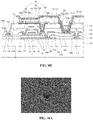
- FIG. 10A and FIG. 10B are scanning electron microscope (SEM) pictures showing a hole and a protrusion part of a connection pattern according to the embodiment of the present disclosure.
- a light-blocking pattern 112 and a first auxiliary electrode 114 are formed in a pixel region P on a substrate 100 on which the pixel region P and a pad region PA are defined by depositing a first conductive material and patterning it through a first mask process.
- a buffer layer 120 is formed on the light-blocking pattern 112 and the first auxiliary electrode 114 by depositing an inorganic insulating material substantially over an entire surface of the substrate 100 and is patterned through a second mask process, thereby forming a buffer hole 120a partially exposing an upper surface of the light-blocking pattern 112.
- a semiconductor layer 122 and a capacitor electrode 124 are formed on the buffer layer 120 by depositing a semiconductor material and patterning it through a third mask process.
- the semiconductor layer 122 and the capacitor electrode 124 are spaced apart from each other over the light-blocking pattern 112.
- the semiconductor material can be polycrystalline silicon, and in this case, both ends of the semiconductor layer 122 and the capacitor electrode 124 can be doped with impurities later.
- the semiconductor material can be formed of an oxide semiconductor material.
- a gate insulation layer 130 and a gate electrode 132 are formed by sequentially depositing an inorganic insulating material and a second conductive material on the semiconductor layer 122 and the capacitor electrode 124 and patterning them through a fourth mask process.
- the gate insulation layer 130 and the gate electrode 132 are disposed to correspond to a center of the semiconductor layer 122.
- a gate insulation pattern 131 and a first pad electrode 134 are formed on the buffer layer 120 in the pad region PA.
- an interlayer insulation layer 140 is formed on the gate electrode 132 and the first pad electrode 134 by depositing an inorganic insulating material or applying an organic insulating material substantially over the entire surface of the substrate 100 and is patterned through a fifth mask process, thereby forming first, second, third, fourth and fifth contact holes 140a, 140b, 140c, 140d, and 140e.
- the buffer layer 120 can also be selectively removed.
- the first and second contact holes 140a and 140b expose the both ends of the semiconductor layer 122.
- the third contact hole 140c partially exposes the upper surface of the light-blocking pattern 112 corresponding to the buffer hole 120a.
- the buffer hole 120a can be omitted, and the third contact hole 140c can be formed in the buffer layer 120 as well as in the interlayer insulation layer 140 to partially expose the upper surface of the light-blocking pattern 112.
- the second mask process is omitted.
- the fourth contact hole 140d is formed in the buffer layer 120 as well as in the interlayer insulation layer 140 to partially expose an upper surface of the first auxiliary electrode 114.
- the fifth contact hole 140e partially exposes an upper surface of the first pad electrode 134.
- source and drain electrodes 142 and 144 and a second auxiliary electrode 146 are formed on the interlayer insulation layer 140 by depositing a third conductive material and patterning it through a sixth mask process.
- a second pad electrode 148 is formed in the pad region PA.
- the source and drain electrodes 142 and 144 are in contact with the both ends of the semiconductor layer 122 through the first and second contact holes 140a and 140b, respectively. Further, the drain electrode 144 is contacts the light-blocking pattern 112 through the third contact hole 140c and overlaps the capacitor electrode 124.
- the second auxiliary electrode 146 contacts the first auxiliary electrode 114 through the fourth contact hole 140d.
- the second pad electrode 148 contacts the first pad electrode 134 through the fifth contact hole 140e.
- the semiconductor layer 122, the gate electrode 132, and the source and drain electrodes 142 and 144 form a thin film transistor T.
- the capacitor electrode 124 overlaps the light-blocking pattern 112 and the drain electrode 144 to form a storage capacitor.
- a passivation layer 150 is formed on the source and drain electrodes 142 and 144, the second auxiliary electrode 146 and the second pad electrode 148 by depositing an inorganic insulating material, and an overcoat layer 155 is formed on the passivation layer 150 by applying an organic insulating material. Then, the passivation layer 150 and the overcoat layer 155 are patterned through a seventh mask process, thereby forming a drain contact hole 155a, a sixth contact hole 155b and a pad hole 155c.
- the drain contact hole 155a partially exposes the drain electrode 144, the sixth contact hole 155b exposes the second auxiliary electrode 146, and the pad hole 155c exposes the second pad electrode 148.
- the passivation layer 150 and the overcoat layer 155 are patterned through the same mask process, but the passivation layer 150 and the overcoat layer 155 can be patterned through different mask processes. That is, after the passivation layer 150 can be formed by depositing an inorganic insulating material and can be patterned through a mask process, the overcoat layer 155 can be formed by applying an organic insulating material and can be patterned through another mask process.
- a first electrode 160 and a connection pattern 162 are formed on the overcoat layer 155 through an eighth mask process.
- a first conductive layer 1601, a second conductive layer 1602, and a third conductive layer 1603 are sequentially deposited on the overcoat layer 155 substantially over the entire surface of the substrate 100.
- the second conductive layer 1602 is formed of silver (Ag).
- the first and third conductive layers 1601 and 1063 can be formed of ITO or IZO, but is not limited thereto.
- a photoresist pattern 200 is formed on the third conductive layer 1603.
- the photoresist pattern 200 is formed on the thin film transistor T and the second auxiliary electrode 146 and overlaps the drain contact hole 155a and the sixth contact hole 155b. Meanwhile, the photoresist pattern 200 corresponding to the sixth contact hole 155b partially exposes an upper surface of the third conductive layer 1603.
- the exposed first, second, and third conductive layers 1601, 1602, and 1603 are removed by using the photoresist pattern 200 as an etching mask.
- the first, second, and third conductive layers 1601, 1602, and 1603 can be removed by a wet etching method using a batch etchant.
- the first, second and third conductive layers 1601, 1602 and 1603 can be removed using different etchants.
- the photoresist pattern 200 is removed.
- the first electrode 160 and the connection pattern 162 are formed on the overcoat layer 155.
- Each of the first electrode 160 and the connection pattern 162 includes a first layer 160a and 162a, a second layer 160b and 162b, and a third layer 160c and 162c.
- the second layer 160b and 162b is disposed between the first layer 160a and 162a and the third layer 160c and 162c
- the third layer 160c and 162c is disposed between the second layer 160b and 162b and the overcoat layer 155.
- the first layer 160a and 162a corresponds to the third conductive layer 1603 of FIG. 9C
- the second layer 160b and 162b corresponds to the second conductive layer 1602 of FIG. 9C
- the third layer 160c and 162c corresponds to the first conductive layer 1601 of FIG. 9C .
- the first electrode 160 is in contact with the drain electrode 144 through the drain contact hole 155a, and the connection pattern 162 is in contact with the second auxiliary electrode 146 through the sixth contact hole 155b.
- connection pattern 162 includes at least one hole 162e in the sixth contact hole 155b, and an upper surface of the second auxiliary electrode 146 is partially exposed through the hole 162e.
- FIG. 10A is an SEM picture showing the hole 162e.
- a first bank 172 of a hydrophilic property is formed on the first electrode 160 and the connection pattern 162 by depositing an insulating material and patterning it through a ninth mask process.
- the first bank 172 overlaps and covers edges of the first electrode 160 and exposes a central portion of the first electrode 160.
- the first bank 172 overlaps and covers edges of the connection pattern 162.
- the first bank 172 has a first auxiliary contact hole 172b exposing a central portion of the connection pattern 162.
- the first bank 172 is removed to correspond to the pad hole 155c, thereby exposing the second pad electrode 148.
- a second bank 174 of a hydrophobic property is formed on the first bank 172 by applying an organic material and patterning it through a tenth mask process.
- a bank material layer (not shown) is formed by applying an organic material
- a photomask (not shown) is disposed over the bank material layer, and the bank material is exposed to light through the photomask.
- the bank material layer can be a negative photosensitive type in which a portion exposed to light remains after developing.
- the bank material layer exposed to light is developed and a portion not exposed to light is removed, thereby forming the second bank 174.
- the present disclosure is not limited thereto, and the bank material layer can be a positive photosensitive type in which a portion not exposed to light remains after developing.
- the second bank 174 is baked.
- the second bank 174 can be baked by heating the substrate 100 on which the second bank 174 is formed in an oven at about 230 degrees Celsius for about an hour.
- FIG. 10B is an SEM picture showing the protrusion part 162d.
- the hydrophilic first bank 172 and the hydrophobic second bank 174 are formed through different mask processes, but the first bank 172 and the second bank 174 can be formed through the same mask process.
- the organic material layer can be exposed to light using a halftone mask, which includes a light-transmitting portion, a light-blocking portion and a half light-transmitting portion, and can be patterned, thereby forming the hydrophilic first bank 172 and the hydrophobic second bank 174.
- a first charge auxiliary layer 182 is formed on the first electrode 160 exposed through the second bank 174 by dropping a first solution and drying it. At least one side surface of the first charge auxiliary layer 182 is enclosed by the second bank 174.
- a drying speed of a solvent in a region adjacent to the second bank 174 is different from that in other regions, and thus a height of the first charge auxiliary layer 182 in the region adjacent to the second bank 174 rises as it gets closer to the second bank 174.
- the first charge auxiliary layer 182 can be a hole injecting layer (HIL) and/or a hole transporting layer (HTL).
- HIL hole injecting layer
- HTL hole transporting layer
- a light-emitting material layer 184 is formed on the first charge auxiliary layer 182 by dropping a second solution and drying it. At least one side surface of the light-emitting material layer 184 is enclosed by the second bank 174.
- a drying speed of a solvent in a region adjacent to the second bank 174 is different from that in other regions, and thus a height of the light-emitting material layer 184 in the region adjacent to the second bank 174 rises as it gets closer to the second bank 174.
- a second charge auxiliary layer 186 is formed on the light-emitting material layer 184 by depositing an organic material and/or an inorganic material.
- the second charge auxiliary layer 186 is formed substantially over the entire surface of the substrate 100. Accordingly, the second charge auxiliary layer 186 is also formed on the second bank 174 and the connection pattern 162.
- the second charge auxiliary layer 186 has a relatively thin thickness on the protrusion part 162d of the connection pattern 162.
- the second charge auxiliary layer 186 can have a hole (not shown) exposing the protrusion part 162d.
- the second charge auxiliary layer 186 can be an electron injecting layer (EIL) and/or an electron transporting layer (ETL).
- EIL electron injecting layer
- ETL electron transporting layer
- the first charge auxiliary layer 182, the light-emitting material layer 184 and the second charge auxiliary layer 186 constitute a light-emitting layer 180.
- a second electrode 190 is formed on the second charge auxiliary layer 186 by depositing a conductive material such as metal.
- the second electrode 190 is formed substantially over the entire surface. Accordingly, the second electrode 190 is also formed over the second bank 174 and the connection pattern 162.
- the second electrode 190 is electrically connected to the connection pattern 162 through the first and second auxiliary contact holes 172b and 174b.
- the second charge auxiliary layer 186 is disposed between the second electrode 190 and the connection pattern 162, and a distance between the second electrode 190 and the protrusion part 162d of the connection pattern 162 is smaller than a distance between the second electrode 190 and a flat part of the connection pattern 162 because the second charge auxiliary layer 186 has the relatively thin thickness on the protrusion part 162d of the connection pattern 162 due the protrusion part 162d. Accordingly, the electrical contact property between the second electrode 190 and the connection pattern 162 can be improved due to the protrusion part 162d of the connection pattern 162.
- the second electrode 190 can be in direct contact with the protrusion part 162d of the connection pattern 162.
- the first electrode 160, the light-emitting layer 180 and the second electrode 190 constitute a light-emitting diode De.
- the first electrode 160 can serve as an anode
- the second electrode 190 can serve as a cathode.
- the hole 162e of FIG. 9E is formed in the connection pattern 162
- the second bank 174 is baked
- the protrusion part 162d is formed in the connection pattern 162 through the migration phenomenon. Accordingly, by electrically connecting the second electrode 190 and the first and second auxiliary electrodes 114 and 146 through the connection pattern 162 having the protrusion part 162d, the electrical contact property between the second electrode 190 and the connection pattern 162 can be improved without increasing the process.
- the thickness of the second charge auxiliary layer 186 on the protrusion part 162d of the connection pattern 162 is smaller than the thickness of the second charge auxiliary layer 186 on the flat part of the connection pattern 162.
- a mask is omitted to thereby reduce the manufacturing costs, and a display device with a large size and high definition can be implemented.
- the light-emitting layers in pixel regions adjacent along one direction, for example, of the same color sub-pixels are connected to each other and formed as one body, thereby reducing or minimizing the deviation in the dropping amount between nozzles and uniformly forming the thicknesses of the light-emitting layers of the sub-pixels. Therefore, the lack of uniformity of the light emitting layers is prevented, thereby effectively preventing the image quality of the display device from being lowered.
- the second electrode is connected to the auxiliary electrode, thereby lowering the resistance of the second electrode, and the protrusion part is formed in the connection pattern for connecting the second electrode and the auxiliary electrode, thereby improving the electrical contact property between the second electrode and the connection pattern.
Landscapes
- Engineering & Computer Science (AREA)
- Microelectronics & Electronic Packaging (AREA)
- Manufacturing & Machinery (AREA)
- Physics & Mathematics (AREA)
- Optics & Photonics (AREA)
- Geometry (AREA)
- Electroluminescent Light Sources (AREA)
- Devices For Indicating Variable Information By Combining Individual Elements (AREA)
Abstract
Description
- The present application claims priority from and the benefit of Republic of Korea Patent Application No.
10-2019-0161471 filed on December 6, 2019 - The present disclosure relates to an electroluminescent display device, and more particularly, to an electroluminescent display device having a large size and high definition and a method of manufacturing the same.
- As one of flat panel display devices, an electroluminescent display device has wide viewing angles as compared with a liquid crystal display device because it is self-luminous and also has advantages of a thin thickness, light weight and low power consumption because a backlight unit is not necessary.
- In addition, the electroluminescent display device is driven by low voltages of direct current (DC) and has a fast response time. Further, the electroluminescent display device is strong against the external impacts and is used in a wide range of temperatures because its components are solids, and particularly, the electroluminescent display device can be manufactured at low costs.
- The electroluminescent display device includes a plurality of pixels, each of which has red, green, and blue sub-pixels, and displays various color images by allowing the red, green, and blue sub-pixels to selectively emit light.
- The red, green and blue sub-pixels have red, green and blue light-emitting layers, respectively, and each light-emitting layer is formed through a vacuum thermal evaporation process in which a luminous material is selectively deposited using a fine metal mask (FMM).
- However, the evaporation process increases manufacturing costs due to preparation of the mask and has a problem in application to a large-sized and high-definition display device due to manufacturing variations, sagging, shadow effect of the mask, and the like.
- Accordingly, the present disclosure is directed to an electroluminescent display device and a method of manufacturing the same that substantially obviate one or more of the problems due to limitations and disadvantages of the related art.
- An object of the present disclosure is to provide an electroluminescent display device having a large size and high definition and a method of manufacturing the same.
- Additional features and advantages of the present disclosure will be set forth in the description which follows, and in part will be apparent from the description, or can be learned by practice of the present disclosure. The objectives and other advantages of the present disclosure will be realized and attained by the structure particularly pointed out in the written description and claims hereof as well as the appended drawings.
- To achieve these and other advantages and in accordance with the purpose of the present disclosure, as embodied and broadly described herein, there is provided an electroluminescent display device that includes a substrate, a first electrode on the substrate, a connection pattern on the substrate and spaced apart from the first electrode, a bank covering edges of the first electrode and the connection pattern, a light-emitting layer on the first electrode, and a second electrode on the light-emitting layer, the bank and the connection pattern, wherein the connection pattern includes at least one protrusion part and a flat part, and wherein each of the first electrode and the connection pattern includes a first layer and a second layer, the second layer is disposed between the substrate and the first layer, and the second layer of the connection pattern has the at least one protrusion part.
- In another aspect, a method of manufacturing an electroluminescent display device comprises forming a first electrode and a connection pattern on a substrate, forming a bank on the first electrode and the connection pattern; forming a light-emitting layer on the first electrode, and forming a second electrode on the light-emitting layer, the bank and the connection pattern, wherein the connection pattern includes at least one protrusion part and a flat part, and wherein each of the first electrode and the connection pattern includes a first layer and a second layer, the second layer is disposed between the substrate and the first layer, and the second layer of the connection pattern has the at least one protrusion part.
- It is to be understood that both the foregoing general description and the following detailed description are by example and explanatory and are intended to provide further explanation of the present disclosure as claimed.
- The accompanying drawings, which are included to provide a further understanding of the present disclosure and which are incorporated in and constitute a part of this specification, illustrate an embodiment of the present disclosure and together with the description serve to explain the principles of the present disclosure.
-
FIG. 1 is a circuit diagram of one pixel region of an electroluminescent display device according to an embodiment of the present disclosure. -
FIG. 2 is a schematic plan view of an electroluminescent display device according to an embodiment of the present disclosure. -
FIG. 3 is a cross-sectional view corresponding to the line I-I' ofFIG. 2 according to an embodiment of the present disclosure. -
FIG. 4 is a cross-sectional view corresponding to the line II-II' ofFIG. 2 according to an embodiment of the present disclosure. -
FIG. 5 is a schematic plan view of a pixel of an electroluminescent display device according to an embodiment of the present disclosure. -
FIG. 6 and FIG. 7 are plan views of enlarging an area A1 ofFIG. 5 according to embodiments of the present disclosure. -
FIG. 8 is a schematic cross-sectional view of an electroluminescent display device according to an embodiment of the present disclosure. -
FIGS. 9A to 9H are cross-sectional views schematically illustrating a manufacturing process of an electroluminescent display device according to an embodiment of the present disclosure. -
FIG. 10A andFIG. 10B are scanning electron microscope (SEM) pictures showing a hole and a protrusion part of a connection pattern according to an embodiment of the present disclosure. - Reference will now be made in detail to an exemplary embodiment of the disclosure, examples of which are illustrated in the accompanying drawings.
- An electroluminescent display device according to an embodiment of the present disclosure includes a plurality of pixels to display an image, and each of the plurality of pixels includes red, green, and blue sub-pixels. A pixel region corresponding to each sub-pixel can have a configuration shown in
FIG. 1 . -
FIG. 1 is a circuit diagram of one pixel region of an electroluminescent display device according to an embodiment of the present disclosure. - In
FIG. 1 , the electroluminescent display device according to the embodiment of the present disclosure includes a plurality of gate lines and a plurality of data lines crossing each other to define a plurality of pixel regions. Particularly, in the example ofFIG. 1 , a gate line GL and a data line DL cross each other to define a pixel region P. A switching thin film transistor Ts, a driving thin film transistor Td, a storage capacitor Cst, and a light-emitting diode De are formed in each pixel region P. - More specifically, a gate electrode of the switching thin film transistor Ts is connected to the gate line GL and a source electrode of the switching thin film transistor Ts is connected to the data line DL. A gate electrode of the driving thin film transistor Td is connected to a drain electrode of the switching thin film transistor Ts and a source electrode of the driving thin film transistor Td is connected to a high voltage supply VDD. An anode of the light-emitting diode De is connected to a drain electrode of the driving thin film transistor Td, and a cathode of the light-emitting diode De is connected to a low voltage supply VSS. The storage capacitor Cst is connected to the gate electrode and the drain electrode of the driving thin film transistor Td.
- The electroluminescent display device is driven to display an image. For example, when the switching thin film transistor Ts is turned on by a gate signal applied through the gate line GL, a data signal from the data line DL is applied to the gate electrode of the driving thin film transistor Td and an electrode of the storage capacitor Cst through the switching thin film transistor Ts.
- When the driving thin film transistor Td is turned on by the data signal, an electric current flowing through the light-emitting diode De is controlled, thereby displaying an image. The light-emitting diode De emits light due to the current supplied through the driving thin film transistor Td from the high voltage supply VDD.
- Namely, the amount of the current flowing through the light-emitting diode De is proportional to the magnitude of the data signal, and the intensity of light emitted by the light-emitting diode De is proportional to the amount of the current flowing through the light-emitting diode De. Thus, the pixel regions P show different gray levels depending on the magnitude of the data signal, and as a result, the electroluminescent display device displays an image.
- In addition, the storage capacitor Cst maintains charges corresponding to the data signal for a frame when the switching thin film transistor Ts is turned off. Accordingly, even if the switching thin film transistor Ts is turned off, the storage capacitor Cst allows the amount of the current flowing through the light-emitting diode De to be constant and the gray level shown by the light-emitting diode De to be maintained until a next frame.
- Meanwhile, one or more thin film transistors and/or capacitors can be added in the pixel region P in addition to the switching and driving thin film transistors Ts and Td and the storage capacitor Cst.
- For example, in the electroluminescent display device, the driving thin film transistor Td is turned on for a relatively long time while the data signal is applied to the gate electrode of the driving thin film transistor Td and the light-emitting diode De emits light to thereby display the gray level. The driving thin film transistor Td can deteriorate due to application of the data signal for a long time. Therefore, the mobility and/or threshold voltage Vth of the driving thin film transistor Td are changed, and thus the pixel region P of the electroluminescent display device displays a different gray level with respect to the same data signal. This causes non-uniform luminance, thereby lowering the image quality of the electroluminescent display device.
- Accordingly, to compensate the change of the mobility and/or threshold voltage of the driving thin film transistor Td, at least one sensing thin film transistor and/or capacitor for sensing a voltage change can be further added in the pixel region P. The sensing thin film transistor and/or capacitor can be connected to a reference line for applying a reference voltage and outputting a sensing voltage.
-
FIG. 2 is a schematic plan view of an electroluminescent display device according to an embodiment of the present disclosure and mainly shows a bank configuration. - In
FIG. 2 , the electroluminescent display device according to the embodiment of the present disclosure includes a display area DA displaying an image and a non-display area NDA surrounding the display area DA. - In the display area DA, red, green, and blue sub-pixels R, G and B are disposed. The red, green, and blue sub-pixels R, G and B are sequentially arranged along a first direction, and the same color sub-pixels R, G, and B are arranged along a second direction. For example, R, G and B sub-pixels are repeatedly arranged in that order along the first direction (e.g., horizontal direction), whereas a column of R sub-pixels, a column of G sub-pixels, and a column of B sub-pixels are repeatedly arranged in that order along the second direction (e.g., vertical direction). Here, the red, green, and blue sub-pixels R, G and B are shown to each have a rectangular shape, but is not limited thereto. The red, green, and blue sub-pixels R, G and B each can have various shapes such as a rectangular shape with rounded corners, an oval shape, or the like.
- In the non-display area NDA, a plurality of dummy sub-pixels DP are disposed. It is illustrated that one dummy sub-pixel DP is disposed at each of left and right sides of each sub-pixel row of the first direction and upper and lower sides of each sub-pixel column of the second direction in the display area DA, the number of the dummy sub-pixel DP is not limited thereto. For example, two or more dummy sub-pixels DP can be disposed at each of the left and right sides of each sub-pixel row, and two or more dummy sub-pixels DP can be disposed at each of the upper and lower sides of each sub-pixel column.
- A bank is disposed to correspond to the sub-pixels R, G, and B of the display area DA and the dummy sub-pixels DP of the non-display area NDA. The bank includes a
first bank 172 of a hydrophilic property and asecond bank 174 of a hydrophobic property. - More specifically, the
first bank 172 is disposed between adjacent same color sub-pixels R, G, and B and between adjacent different color sub-pixels R, G and B in the display area DA. Thefirst bank 172 can surround each sub-pixel R, G, and B. - Alternatively, the
first bank 172 can be omitted between the adjacent different color sub-pixels R, G and B. That is, thefirst bank 172 can be formed between the adjacent sub-pixels R, G and B along the second direction and can extend along the first direction. - The
second bank 174 is disposed on thefirst bank 172. Thesecond bank 174 has anopening 174a corresponding to a same color sub-pixel column and is disposed between adjacent different color sub-pixels R, G and B. Theopening 174a can extend into the dummy sub-pixel DP adjacent to the same color sub-pixel column along the second direction. - In addition, the
opening 174a is also formed to correspond to a dummy sub-pixel column along the second direction. - Accordingly, the
opening 174a extends in the second direction, and theopening 174a has a length of the second direction longer than a length of the first direction. That is, theopening 174a has a short side parallel to the first direction and a long side parallel to the second direction. At this time, thesecond bank 174 can have a narrower width than thefirst bank 172 between adjacent different color sub-pixels R, G and B. - A cross-sectional structure of the electroluminescent display device according to the embodiment of the present disclosure will be described with reference to
FIG. 3 and FIG. 4 . -
FIG. 3 is a cross-sectional view corresponding to the line I-I' ofFIG. 2 , andFIG. 4 is a cross-sectional view corresponding to the line II-II' ofFIG. 2 according to embodiments of the present disclosure. - In
FIG. 3 and FIG. 4 , a plurality of pixel regions P respectively corresponding to red, green and blue sub-pixels R, G and B and a dummy sub-pixel region DP are defined on asubstrate 100, and abuffer layer 120, thin film transistors T, apassivation layer 150 and anovercoat layer 155 are sequentially formed on thesubstrate 100. - Here, the thin film transistor T includes a gate electrode, a semiconductor layer, and source and drain electrodes, and this will be described in detail later.
- Although not shown in the figure, one or more insulation layers can be further formed between the
buffer layer 120 and thepassivation layer 150. - In each pixel region P, the
overcoat layer 155 has adrain contact hole 155a exposing a part of the thin film transistor T, that is, a drain electrode together with thepassivation layer 150. - A
first electrode 160 is formed in each pixel region P on theovercoat layer 155, and adummy electrode 164 is formed in the dummy sub-pixel region DP on theovercoat layer 155. Thefirst electrode 160 contacts the drain electrode of the thin film transistor T through thedrain contact hole 155a. - On the other hand, the
passivation layer 150 and theovercoat layer 155 do not have a drain contact hole in the dummy sub-pixel region DP, and thedummy electrode 164 is not connected to the thin film transistor T in the dummy sub-pixel region DP. - Meanwhile, the
dummy electrode 164 and the thin film transistor T in the dummy sub-pixel region DP are formed such that a top surface in the dummy sub-pixel region DP may be substantially flush with that in the pixel region P. At least one of thedummy electrode 164 and the thin film transistor T can be omitted in the dummy sub-pixel region DP. - A
first bank 172 of a hydrophilic property is formed on thefirst electrode 160 and thedummy electrode 164. Thefirst bank 172 overlaps and covers edges of thefirst electrode 160 of the pixel region P. Thefirst bank 172 is formed between adjacent same color sub-pixels R, G and B and between adjacent different color sub-pixels R, G and B. Alternatively, thefirst bank 172 can be omitted between adjacent different color sub-pixels R, G and B and can be disposed only between adjacent same color sub-pixels R, G and B. - In addition, the
first bank 172 overlaps and covers edges of thedummy electrode 164 of the dummy sub-pixel region DP. - The
first bank 172 can be formed of a material having a hydrophilic property, for example, an inorganic insulating material such as silicon oxide (SiO2) or silicon nitride (SiNx). Alternatively, thefirst bank 172 can be formed of polyimide. - A
second bank 174 of a hydrophobic property is formed on thefirst bank 172. Thesecond bank 174 has a thicker thickness than thefirst bank 172. Thesecond bank 174 may be formed only between adjacent different color sub-pixels R, G and B and is not formed between adjacent same color sub-pixels R, G and B. A width of thesecond bank 174 is narrower than a width of thefirst bank 172 between adjacent different color sub-pixels R, G and B. - The
second bank 174 has anopening 174a corresponding to a same color sub-pixel column and exposes thefirst electrodes 162 of the same color sub-pixel column and thefirst bank 172 between adjacentfirst electrodes 162 through theopening 174a. In addition, theopening 174a extends into the dummy sub-pixel region DP adjacent to the same color sub-pixel row, and thedummy electrode 164 is exposed through theopening 174a. - Here, when the
first bank 172 is omitted between adjacent different color sub-pixels R, G and B, thesecond bank 174 contacts and overlaps edges of eachfirst electrode 160 ofFIG. 3 and covers the edges of eachfirst electrode 160 ofFIG. 3 . - The
second bank 174 can be formed of an organic insulating material having a hydrophobic property. Alternatively, thesecond bank 174 can be formed of an organic insulating material having a hydrophilic property and can be subjected to a hydrophobic treatment. - The
first bank 172 and thesecond bank 174 can be formed of the same material and formed as one body. At this time, thefirst bank 172 and thesecond bank 174 can be formed through a half-tone mask process. - A light-emitting
layer 180 is formed on thefirst electrode 160 exposed through theopening 174a of thesecond bank 174 in each pixel region P. Here, a red light-emitting layer is formed in the red sub-pixel R, a green light-emitting layer is formed in the green sub-pixel G, and a blue light-emitting layer is formed in the blue sub-pixel B. - In addition, the light-emitting
layer 180 is also formed on thefirst bank 172 exposed through theopening 174a of thesecond bank 174 between adjacent same color sub-pixels R, G and B. Namely, inFIG. 4 , the green light-emittinglayer 180 is also formed on thefirst bank 172 exposed through theopening 174a of thesecond bank 174 between adjacent green sub-pixels G. At this time, the light-emittinglayer 180 on thefirst bank 172 is connected to the light-emittinglayer 180 on thefirst electrode 160 in each pixel region P adjacent thereto to thereby form one body. - A dummy light-emitting
layer 180a is formed on thedummy electrode 164 in the dummy sub-pixel region DP. Referring toFIG. 3 , the dummy light-emittinglayer 180a of the dummy sub-pixel region DP is spaced apart from the light-emittinglayer 180 of the pixel region P adjacent thereto along the first direction, and referring toFIG. 4 , the dummy light-emittinglayer 180a of the dummy sub-pixel region DP is connected to the light-emittinglayer 180 of the pixel region P adjacent thereto along the second direction to thereby form one body. - The light-emitting
layer 180 is formed through a solution process. Here, the solutions dropped into respective pixel regions P corresponding to the same color sub-pixels, for example, the green sub-pixel column through different nozzles are connected to each other, and the light-emittinglayer 180 is formed by drying the solutions. Accordingly, a deviation in the dropping amounts between the nozzles is minimized, and thicknesses of the light-emittinglayers 180 can be uniform in the respective pixel regions P. At this time, the dummy light-emittinglayer 180a is formed simultaneously with the light-emittinglayer 180. - Heights of the light-emitting
layer 180 and the dummy light-emittinglayer 180a formed through the solution process rise around thesecond bank 174 as it gets closer to thesecond bank 174. - Next, a
second electrode 190 is formed on the light-emittinglayer 180 and the dummy light-emittinglayer 180a. Thesecond electrode 190 is also formed on a top surface and a side surface of thesecond bank 174. - The
first electrode 160, the light-emittinglayer 180, and thesecond electrode 190 constitute a light-emitting diode De. - The electroluminescent display device according to the embodiment of the present disclosure is a top emission type in which light of a light-emitting diode De is output toward a direction opposite the
substrate 100, that is, output to the outside through thesecond electrode 190. The top emission type display device can have a wider emission area than a bottom emission type display device of the same size, to thereby improve luminance and reduce power consumption. - To transmit light, the
second electrode 190 can be formed of a metal material so as to have a thin thickness or formed of a transparent conductive material. Accordingly, the resistance of thesecond electrode 190 increases, and a voltage drop occurs due to the resistance, thereby causing a problem of non-uniform brightness. - In the present disclosure, to lower the resistance of the
second electrode 190, thesecond electrode 190 is electrically connected to an auxiliary electrode. At this time, thesecond electrode 190 and the auxiliary electrode are electrically connected through a connection pattern, and to improve an electrical contact property between the connection pattern and thesecond electrode 190, a protrusion part is formed in the connection pattern. - The configuration of the electroluminescent display device according to the embodiment of the present disclosure will be described with reference to
FIGS. 5 to 7 . -
FIG. 5 is a schematic plan view of a pixel of an electroluminescent display device according to an embodiment of the present disclosure and mainly shows a bank configuration.FIG. 6 and FIG. 7 are plan views of enlarging an area A1 ofFIG. 5 according to embodiments of the present disclosure. - In
FIG. 5 ,FIG. 6, and FIG. 7 , one pixel of the electroluminescent display device according to the embodiment of the present disclosure includes red, green, and blue sub-pixels R, G and B sequentially arranged along a first direction. - Here, the red, green, and blue sub-pixels R, G and B may have different sizes. The sizes of the red, green, and blue sub-pixels R, G and B are determined by considering the lifetime of a light-emitting diode provided at each sub-pixel. For example, the size of the green sub-pixel G may be larger than the size of the red sub-pixel R and smaller than the size of the blue sub-pixel B.
- The red, green, and blue sub-pixels R, G, and B can be defined by first and
second banks - More specifically, the
first bank 172 is disposed between adjacent same color sub-pixels R, G and B and between adjacent different color sub-pixels R, G and B. Thefirst bank 172 can surround each sub-pixel R, G and B. - Alternatively, the
first bank 172 can be omitted between the adjacent different color sub-pixels R, G and B. That is, thefirst bank 172 can be formed only between the adjacent sub-pixels R, G and B along a second direction perpendicular to the first direction and can extend in the first direction. - Next, the
second bank 174 is formed on thefirst bank 172. Thesecond bank 174 has anopening 174a corresponding to a same color sub-pixel column and is disposed between adjacent different color sub-pixels R, G and B along the first direction. - The
second bank 174 extends substantially in the second direction, and at least one side of thesecond bank 174 has anextension 174c extending in the first direction. At this time, theextension 174c can be disposed between the adjacent same color sub-pixels R, G and B along the second direction and can overlap thefirst bank 172. Theextension 174c reduces a distance between adjacent portions of thesecond bank 174 and controls the flow of a solution during a solution process for forming a light-emitting layer, so that the light-emitting layer is uniformly formed. - The size of the
extension 174c can vary according to the size of each sub-pixel R, G, and B. - Meanwhile, the
first bank 172 and thesecond bank 174 have first and second auxiliary contact holes 172b and 174b corresponding to at least oneextension 174c, respectively. - An
auxiliary electrode 146 and aconnection pattern 162 are formed to correspond to theextension 174c. Theconnection pattern 162 is exposed through the first and second auxiliary contact holes 172b and 174b. - In addition, although not shown in the figure, at least one insulation layer may be formed between the
auxiliary electrode 146 and theconnection pattern 162. Theauxiliary electrode 146 and theconnection pattern 162 are in contact with each other through a contact hole formed in the at least one insulation layer. - Meanwhile, the
connection pattern 162 has at least oneprotrusion part 162d. - As shown in
FIG. 6 , theprotrusion part 162d may have a dot shape. Alternatively, as shown inFIG. 7 , theprotrusion part 162d may have a slit shape having a width and a length different from each other. In this case, the length of theprotrusion part 162d can be the same as a length of theconnection pattern 162. The protrusion part protrudes in a direction away from the substrate, optionally in the direction parallel to the normal of the substrate. - It is preferable that a diameter or the width of the
protrusion part 162d is 2 µm to 4 µm. - Although it is illustrated that there is only one
protrusion part 162d, the number of theprotrusion parts 162d is not limited thereto. Namely, a plurality of protrusion parts can be formed according to the size of theconnection pattern 162 exposed through the first and second auxiliary contact holes 172b and 174b. - At this time, if the
protrusion parts 162d are too many, defects can be caused due to particles. Accordingly, it is beneficial that the total size of the plurality ofprotrusion parts 162d is less than 5% of the size of theconnection pattern 162 exposed through the first and second auxiliary contact holes 172b and 174b. - Meanwhile, although not shown in the figure, a
second electrode 190 ofFIGS. 3 and 4 is formed on the first andsecond banks connection pattern 162, and thesecond electrode 190 is electrically connected to theauxiliary electrode 146 through theconnection pattern 162. - A part of the light-emitting
layer 180 ofFIGS. 3 and 4 can be formed between theconnection pattern 162 and thesecond electrode 190, and thus an electrical contact property between theconnection pattern 162 and thesecond electrode 190 can be lowered. However, in the present disclosure, since theconnection pattern 162 has theprotrusion part 162d, a distance between theconnection pattern 162 and thesecond electrode 190 decreases, and the electrical contact property between theconnection pattern 162 and thesecond electrode 190 can be improved. - The configuration of the electroluminescent display device including the
connection pattern 162 having theprotrusion part 162d will be described in more detail with reference toFIG. 8 . -
FIG. 8 is a schematic cross-sectional view of an electroluminescent display device according to the embodiment of the present disclosure and shows a pixel region P and a pad region PA. The pixel region P is disposed in a display area displaying an image, and the pad region PA is disposed in a non-display area surrounding the display area. - In
FIG. 8 , a light-blockingpattern 112 and a firstauxiliary electrode 114 of a first conductive material such as metal are formed in the pixel region P on asubstrate 100. Thesubstrate 100 may be a glass substrate or a plastic substrate. For example, polyimide may be used for the plastic substrate, but is not limited thereto. - The light-blocking
pattern 112 and the firstauxiliary electrode 114 can be formed of at least one of aluminum (Al), copper (Cu), molybdenum (Mo), titanium (Ti), chromium (Cr), nickel (Ni), tungsten (W) or an alloy thereof and can have a single-layered structure or a multi-layered structure. For example, the light-blockingpattern 112 and the firstauxiliary electrode 114 can have a double-layered structure including a lower layer of a molybdenum-titanium alloy (MoTi) and an upper layer of copper (Cu), and the upper layer can have a thicker thickness than the lower layer. - A
buffer layer 120 is formed on the light-blockingpattern 112 and the firstauxiliary electrode 114 substantially on an entire surface of thesubstrate 100. Thebuffer layer 120 can be formed of an inorganic insulating material such as silicon oxide (SiO2) or silicon nitride (SiNx) and can be formed as a single layer or multi layers. - Here, the
buffer layer 120 has abuffer hole 120a on the light-blockingpattern 112, and an upper surface of the light-blockingpattern 112 is partially exposed through thebuffer hole 120a. - A
semiconductor layer 122 and acapacitor electrode 124 are patterned and formed on thebuffer layer 120. Thesemiconductor layer 122 and thecapacitor electrode 124 are spaced apart from each other over the light-blockingpattern 112. The light-blockingpattern 112 blocks light incident on thesemiconductor layer 122 and prevents thesemiconductor layer 122 from deteriorating due to the light. - The
semiconductor layer 122 and thecapacitor electrode 124 can be formed of polycrystalline silicon, and in this case, both ends of thesemiconductor layer 122 and thecapacitor electrode 124 can be doped with impurities. Alternatively, thesemiconductor layer 122 and thecapacitor electrode 124 can be formed of an oxide semiconductor material. - A
gate insulation layer 130 of an insulating material and agate electrode 132 of a second conductive material are sequentially formed on thesemiconductor layer 122. Thegate insulation layer 130 and thegate electrode 132 are disposed to correspond to a center of thesemiconductor layer 122. - The
gate insulation layer 130 can be formed of an inorganic insulating material such as silicon oxide (SiO2) or silicon nitride (SiNx). When thesemiconductor layer 122 is made of an oxide semiconductor material, it is preferable that thegate insulation layer 130 is formed of silicon oxide (SiO2). - Alternatively, when the
semiconductor layer 122 is made of polycrystalline silicon, thegate insulation layer 130 can be formed of silicon oxide (SiO2) or silicon nitride (SiNx). - The
gate electrode 132 can be formed of at least one of aluminum (Al), copper (Cu), molybdenum (Mo), titanium (Ti), chromium (Cr), nickel (Ni), tungsten (W) or an alloy thereof and can have a single-layered structure or a multi-layered structure. For example, thegate electrode 132 can have a double-layered structure including a lower layer of a molybdenum-titanium alloy (MoTi) and an upper layer of copper (Cu), and the upper layer can have a thicker thickness than the lower layer. - As shown in the figure, the
gate insulation layer 130 can be patterned to have the same shape as thegate electrode 132. At this time, a width of thegate insulation layer 130 can be larger than a width of thegate electrode 132, and thus, edges of an upper surface of thegate insulation layer 130 can be exposed. Alternatively, the width of thegate insulation layer 130 can be the same as the width of thegate electrode 132. - Or, the
gate insulation layer 130 may not be patterned and can be formed substantially over the entire surface of thesubstrate 100. - Meanwhile, a gate line (not shown) can be further formed of the same material and on the same layer as the
gate electrode 132. - In addition, a
gate insulation pattern 131 and afirst pad electrode 134 are sequentially formed on thebuffer layer 120 in the pad region PA. Thegate insulation pattern 131 can be formed of the same material as thegate insulation layer 130, and thefirst pad electrode 134 can be formed of the same material as thegate electrode 132. Thegate insulation pattern 131 can be patterned to have the same shape as thefirst pad electrode 134. At this time, a width of thegate insulation pattern 131 can be larger than a width of thefirst pad electrode 134, and edges of an upper surface of thegate insulation pattern 131 can be exposed. Alternatively, the width of thegate insulation pattern 131 can be the same as the width of thefirst pad electrode 134. - An
interlayer insulation layer 140 made of an insulating material is formed on thegate electrode 132 substantially over the entire surface of thesubstrate 100. Theinterlayer insulation layer 140 can be formed of an inorganic insulating material such as silicon oxide (SiO2) or silicon nitride (SiNx). Alternatively, theinterlayer insulation layer 140 can be formed of an organic insulating material such as photo acryl or benzocyclobutene. - The
interlayer insulation layer 140 has first, second, third andfourth contact holes second contact holes semiconductor layer 122. Thethird contact hole 140c partially exposes the upper surface of the light-blockingpattern 112 and is located in thebuffer hole 120a. Alternatively, thebuffer hole 120a may be omitted, and thethird contact hole 140c can be formed in thebuffer layer 120 as well as in theinterlayer insulation layer 140 to partially expose the upper surface of the light-blockingpattern 112. Thefourth contact hole 140d is formed in thebuffer layer 120 as well as in theinterlayer insulation layer 140 to partially expose an upper surface of the firstauxiliary electrode 114. - The
interlayer insulation layer 140 is also formed on thefirst pad electrode 134 in the pad region PA and has afifth contact hole 140e partially exposing an upper surface of thefirst pad electrode 134. - Source and
drain electrodes auxiliary electrode 146 made of a third conductive material such as metal are formed on theinterlayer insulation layer 140. The source and drainelectrodes auxiliary electrode 146 can be formed of at least one of aluminum (Al), copper (Cu), molybdenum (Mo), titanium (Ti), chromium (Cr), nickel (Ni), tungsten (W) or an alloy thereof and can have a single-layered structure or a multi-layered structure. For example, the source and drainelectrodes auxiliary electrode 146 can have a double-layered structure including a lower layer of a molybdenum-titanium alloy (MoTi) and an upper layer of copper (Cu), and the upper layer can have a thicker thickness than the lower layer. Alternatively, the source and drainelectrodes auxiliary electrode 146 can have a triple-layered structure. - The source and drain
electrodes gate electrode 132 positioned therebetween. The source and drainelectrodes semiconductor layer 122 through the first andsecond contact holes drain electrode 144 contacts the light-blockingpattern 112 through thethird contact hole 140c. Thecapacitor electrode 124 overlaps the light-blockingpattern 112 and thedrain electrode 144 to form a storage capacitor. - Meanwhile, the second
auxiliary electrode 146 contacts the firstauxiliary electrode 114 through thefourth contact hole 140d. - In addition, a data line (not shown) and a high voltage supply line (not shown) can be further formed on the
interlayer insulation layer 140 and can be made of the third conductive material. - The
semiconductor layer 122, thegate electrode 132, and the source and drainelectrodes gate electrode 132 and the source and drainelectrodes semiconductor layer 122. - Alternatively, the thin film transistor T can have an inverted staggered structure in which the gate electrode and the source and drain electrodes are located at different sides with respect to the semiconductor layer. That is, the gate electrode can be disposed under the semiconductor layer, and the source and drain electrodes can be disposed over the semiconductor layer. In this case, the semiconductor layer can be formed of oxide semiconductor or amorphous silicon.
- The thin film transistor T corresponds to a driving thin film transistor Td of
FIG. 1 , and a switching thin film transistor Ts ofFIG. 1 having the same structure as the driving thin film transistor Td can be further formed on thesubstrate 100. Thegate electrode 132 of the driving thin film transistor can be connected to a drain electrode of the switching thin film transistor, and thesource electrode 142 of the driving thin film transistor is connected to the power supply line. In addition, a gate electrode and a source electrode of the switching thin film transistor can be connected to the gate line and the data line, respectively. - In addition, a
second pad electrode 148 is formed on theinterlayer insulation layer 140 in the pad region PA. Thesecond pad electrode 148 is formed of the same material as the source and drainelectrodes first pad electrode 134 through thefifth contact hole 140e. - A
passivation layer 150 of an insulating material is formed on the source and drainelectrodes auxiliary electrode 146 substantially over the entire surface of thesubstrate 100. Thepassivation layer 150 can be formed of an inorganic insulating material such as silicon oxide (SiO2) or silicon nitride (SiNx). - Next, an
overcoat layer 155 of an insulating material is formed on thepassivation layer 150 substantially over the entire surface of thesubstrate 100. Theovercoat layer 155 can be formed of an organic insulating material such as photo acryl or benzocyclobutene. Theovercoat layer 155 can eliminate level differences due to lower layers and have a substantially flat top surface. - Here, one of the
passivation layer 150 and theovercoat layer 155 can be omitted. For example, thepassivation layer 150 can be omitted, but is not limited thereto. - The
passivation layer 150 and theovercoat layer 155 have adrain contact hole 155a exposing thedrain electrode 144. Further, thepassivation layer 150 and theovercoat layer 155 have asixth contact hole 155b exposing the secondauxiliary electrode 146. - Meanwhile, the
passivation layer 150 and theovercoat layer 155 are also formed in the pad region PA. Thepassivation layer 150 and theovercoat layer 155 of the pad region PA have apad hole 155c exposing thesecond pad electrode 148. At this time, theovercoat layer 155 of the pad region PA is partially removed, thereby exposing thepassivation layer 150 thereunder. Accordingly, the level difference between the layers formed on thesecond pad electrode 148 is lowered, and it is possible to facilitate contact with external circuit. - A
first electrode 160 is formed on theovercoat layer 155 in the pixel region P and formed of a conductive material. Thefirst electrode 160 is in contact with thedrain electrode 144 through thedrain contact hole 155a. - The
first electrode 160 includes afirst layer 160a and asecond layer 160b, and thesecond layer 160b is disposed between thefirst layer 160a and thesubstrate 100, more particularly, between thefirst layer 160a and theovercoat layer 155. - The
first layer 160a is formed of a conductive material having relatively high work function. For example, thefirst layer 160a can be formed of a transparent conductive material such as indium tin oxide (ITO) or indium zinc oxide (IZO). Thesecond layer 160b is formed of a metal material having relatively high reflectance. For example, thesecond layer 160b can be formed of silver (Ag). Here, the work function of thefirst layer 160a is higher than the work function of thesecond layer 160b. - A thickness of the
second layer 160b can be larger than a thickness of thefirst layer 160a. For example, the thickness of thesecond layer 160b can be 80 nm to 100 nm, and the thickness of thefirst layer 160a can be 10 nm to 80 nm. However, the present disclosure is not limited thereto. - In addition, the
first electrode 160 can further include athird layer 160c between thesecond layer 160b and thesubstrate 100, for example, between thesecond layer 160b and theovercoat layer 155. Thethird layer 160c is formed to improve the adhesion property between thesecond layer 160b and theovercoat layer 155 and can be omitted. For example, thethird layer 160c can be formed of a transparent conductive material such as ITO or IZO, but is not limited thereto. - A thickness of the
third layer 160c can be smaller than the thickness of thesecond layer 160b and can be smaller than or equal to the thickness of thefirst layer 160a. For example, the thickness of thethird layer 160c can be 10 nm, but is not limited thereto. - In addition, a
connection pattern 162 is formed on theovercoat layer 155 and is formed of the same material as thefirst electrode 160. Accordingly, theconnection pattern 162 can include first, second andthird layers 162a, 162b, and 162c. At this time, the second layer 162b is disposed between thefirst layer 162a and the third layer 162c, and the third layer 162c is disposed between the second layer 162b and thesubstrate 100, more particularly, between the second layer 162b and theovercoat layer 155. Theconnection pattern 162 is in contact with the secondauxiliary electrode 146 through thesixth contact hole 155b. - The
connection pattern 162 includes at least oneprotrusion part 162d and a flat part in thesixth contact hole 155b. The flat part corresponds to a part excluding theprotrusion part 162d. A height of theprotrusion part 162d is higher than a height of the flat part. - Here, the
first layer 162a and the third layer 162c of theconnection pattern 162 have a hole corresponding to theprotrusion part 162d. Accordingly, a lower surface of the second layer 162b can be in contact with the secondauxiliary electrode 146 through the hole of the third layer 162c. In addition, an upper surface of the second layer 162b protrudes above through the hole of thefirst layer 162a to thereby form theprotrusion part 162d of theconnection pattern 162. That is, the second layer 162b of theconnection pattern 162 has substantially theprotrusion part 162d. - Meanwhile, as described above, when the
third layer 160c of thefirst electrode 160 is omitted and thefirst electrode 160 is configured as double layers, the third layer 162c of theconnection pattern 162 is also omitted. - A bank of an insulating material is formed on the
first electrode 160. The bank includes afirst bank 172 of a hydrophilic property and asecond bank 174 of a hydrophobic property. - More particularly, the
first bank 172 overlaps and covers edges of thefirst electrode 160 and exposes a central portion of thefirst electrode 160. In addition, thefirst bank 172 is also formed on theconnection pattern 162 and overlaps and covers edges of theconnection pattern 162. Thefirst bank 172 has a firstauxiliary contact hole 172b exposing a central portion of theconnection pattern 162. - The
first bank 172 can be formed of a material having a hydrophilic property, for example, an inorganic insulating material such as silicon oxide (SiO2) or silicon nitride (SiNx). Alternatively, thefirst bank 172 can be formed of polyimide. - Meanwhile, the
first bank 172 can also be formed in the pad region PA. Thebank 172 is removed to correspond to thepad hole 155c, thereby exposing thesecond pad electrode 148. - The
second bank 174 is formed on thefirst bank 172. At this time, at least an upper surface of thesecond bank 174 is hydrophobic, and a side surface of thesecond bank 174 can be hydrophobic or hydrophilic. - The
second bank 174 has an opening exposing the central portion of thefirst electrode 160. As described above, the opening of thesecond bank 174 can be formed to correspond to the same color sub-pixel column. - The
second bank 174 is disposed on thefirst bank 172 with a narrower width than thefirst bank 172 and exposes edges of thefirst bank 172. In addition, a thickness of thesecond bank 174 can be larger than a thickness of thefirst bank 172. - The
second bank 174 can be formed of an organic insulating material having a hydrophobic property. Alternatively, thesecond bank 174 can be formed of an organic insulating material having a hydrophilic property and subjected to a hydrophobic treatment. - Further, the
second bank 174 has a secondauxiliary contact hole 174b corresponding to the firstauxiliary contact hole 172b. Theconnection pattern 162 is exposed through the first and second auxiliary contact holes 172b and 174b. - The
connection pattern 162 and the first and second auxiliary contact holes 172b and 174b can be omitted in some pixel regions. - Meanwhile, only the
first bank 172 can be disposed on other edges of thefirst electrode 160 not shown in the figure. - In addition, the
first bank 172 and thesecond bank 174 are formed of different materials and are separate parts as inFIG. 8 . However, the hydrophilicfirst bank 172 and the hydrophobicsecond bank 174 can be formed of the same material and formed as one body. - A light-emitting
layer 180 is formed on thefirst electrode 160 exposed by the first andsecond banks layer 180 can include a first chargeauxiliary layer 182, a light-emittingmaterial layer 184, and a second chargeauxiliary layer 186 that are sequentially positioned over thefirst electrode 160. The light-emittingmaterial layer 184 can be formed of any one of red, green and blue luminescent materials, but is not limited thereto. The luminescent material can be an organic luminescent material such as a phosphorescent compound or a fluorescent compound or can be an inorganic luminescent material such as a quantum dot. - The first charge
auxiliary layer 182 can be a hole auxiliary layer, and the hole auxiliary layer can include at least one of a hole injecting layer (HIL) and a hole transporting layer (HTL). In addition, the second chargeauxiliary layer 186 can be an electron auxiliary layer, and the electron auxiliary layer can include at least one of an electron injecting layer (EIL) and an electron transporting layer (ETL). However, the present disclosure is not limited thereto. - Here, each of the first charge
auxiliary layer 182 and the light-emittingmaterial layer 184 is formed through a solution process. Thus, the process can be simplified and a display device with a large size and high resolution can be provided. A spin coating method, an ink jet printing method, or a screen printing method can be used as the solution process, but the present disclosure is not limited thereto. When the solution is dried, a drying speed of a solvent in a region adjacent to thesecond bank 174 is different from that in other regions. That is, the drying speed of the solvent in the region adjacent to thesecond bank 174 is faster than that in the other regions. Therefore, a height of each of the first chargeauxiliary layer 182 and the light-emittingmaterial layer 184 in the region adjacent to thesecond bank 174 can rise as it gets closer to thesecond bank 174. - On the other hand, the second charge
auxiliary layer 186 is formed through a thermal evaporation process. Accordingly, the second chargeauxiliary layer 186 is formed substantially over the entire surface of thesubstrate 100. That is, the second chargeauxiliary layer 186 is formed on the upper surface and the side surface of thesecond bank 174 and is also formed on theconnection pattern 162. At this time, the second chargeauxiliary layer 186 has a relatively thin thickness on theprotrusion part 162d of theconnection pattern 162. Namely, the thickness of the second chargeauxiliary layer 186 on theprotrusion part 162d of theconnection pattern 162 is smaller than the thickness of the second chargeauxiliary layer 186 on the flat part of theconnection pattern 162. - A
second electrode 190 of a conductive material having a relatively low work function is formed on the light-emittinglayer 180, thesecond bank 174, and theconnection pattern 162 substantially over the entire surface of thesubstrate 100. Thesecond electrode 190 can be formed of aluminum (Al), magnesium (Mg), silver (Ag), or an alloy thereof. At this time, thesecond electrode 190 has a relatively thin thickness such that light from the light-emittinglayer 180 can be transmitted therethrough. For example, thesecond electrode 190 can have the thickness of 5 nm to 10 nm. - Alternatively, the
second electrode 190 can be formed of a transparent conductive material such as indium-gallium-oxide (IGO) or IZO, but is not limited thereto. - The
second electrode 190 is electrically connected to theconnection pattern 162 through the first and second auxiliary contact holes 172b and 174b. At this time, a distance between thesecond electrode 190 and theprotrusion part 162d of theconnection pattern 162 is smaller than a distance between thesecond electrode 190 and the flat part of theconnection pattern 162. Accordingly, the electrical contact property between thesecond electrode 190 and theconnection pattern 162 can be improved due to theprotrusion part 162d of theconnection pattern 162. Here, thesecond electrode 190 can be in direct contact with theprotrusion part 162d of theconnection pattern 162. - The
first electrode 160, the light-emittinglayer 180 and thesecond electrode 190 constitute a light-emitting diode De. Thefirst electrode 160 can serve as an anode, and thesecond electrode 190 can serve as a cathode, but is not limited thereto. - As described above, the electroluminescent display device according to the embodiment of the present disclosure can be a top emission type in which light from the light-emitting
layer 180 of the light-emitting diode De is output toward a direction opposite thesubstrate 100, that is, output to the outside through thesecond electrode 190. The top emission type display device can have a wider emission area than a bottom emission type display device of the same size, to thereby improve luminance and reduce power consumption. - At this time, the light-emitting diode De of each pixel region P can have an element thickness for a micro-cavity effect corresponding to a wavelength of the emitted light, thereby increasing the light efficiency.
- In the meantime, although not shown in the figure, a capping layer can be formed on the
second electrode 190 substantially over the entire surface of thesubstrate 100. The capping layer can be formed of an insulating material having a relatively high refractive index. The wavelength of light traveling along the capping layer can be amplified by surface plasma resonance, and thus the intensity of the peak can be increased, thereby improving the light efficiency in the top emission type electroluminescent display device. For example, the capping layer can be formed as a single layer of an organic layer or an inorganic layer or formed as organic/inorganic stacked layers. - As described above, in the electroluminescent display device according to the embodiment of the present disclosure, by forming some of the light-emitting
layer 180 through the solution process, a mask is omitted to thereby reduce the manufacturing costs, and a display device with a large size and high definition can be implemented. - In addition, the electroluminescent display device according to the embodiment of the present disclosure is implemented as the top emission type, thereby improving the luminance and reducing the power consumption. Here, since the
second electrode 190 is formed to have the relatively thin thickness in order to transmit light, the resistance of thesecond electrode 190 can be increased, but the resistance of thesecond electrode 190 can be lowered by connecting thesecond electrode 190 to the first and secondauxiliary electrodes connection pattern 162. At this time, by forming theprotrusion part 162d in theconnection pattern 162, the electrical contact property between thesecond electrode 190 and theconnection pattern 162 can be improved. - A manufacturing process of an electroluminescent display device according to the embodiment of the present disclosure will be described in detail with reference to
FIGS. 9A to 9H . -
FIGS. 9A to 9H are cross-sectional views schematically illustrating a manufacturing process of an electroluminescent display device according to the embodiment of the present disclosure and show a pixel region P and a pad region PA.FIG. 10A andFIG. 10B are scanning electron microscope (SEM) pictures showing a hole and a protrusion part of a connection pattern according to the embodiment of the present disclosure. - In
FIG. 9A , a light-blockingpattern 112 and a firstauxiliary electrode 114 are formed in a pixel region P on asubstrate 100 on which the pixel region P and a pad region PA are defined by depositing a first conductive material and patterning it through a first mask process. - Next, a
buffer layer 120 is formed on the light-blockingpattern 112 and the firstauxiliary electrode 114 by depositing an inorganic insulating material substantially over an entire surface of thesubstrate 100 and is patterned through a second mask process, thereby forming abuffer hole 120a partially exposing an upper surface of the light-blockingpattern 112. - Then, a
semiconductor layer 122 and acapacitor electrode 124 are formed on thebuffer layer 120 by depositing a semiconductor material and patterning it through a third mask process. Thesemiconductor layer 122 and thecapacitor electrode 124 are spaced apart from each other over the light-blockingpattern 112. - The semiconductor material can be polycrystalline silicon, and in this case, both ends of the
semiconductor layer 122 and thecapacitor electrode 124 can be doped with impurities later. Alternatively, the semiconductor material can be formed of an oxide semiconductor material. - A
gate insulation layer 130 and agate electrode 132 are formed by sequentially depositing an inorganic insulating material and a second conductive material on thesemiconductor layer 122 and thecapacitor electrode 124 and patterning them through a fourth mask process. Thegate insulation layer 130 and thegate electrode 132 are disposed to correspond to a center of thesemiconductor layer 122. In addition, agate insulation pattern 131 and afirst pad electrode 134 are formed on thebuffer layer 120 in the pad region PA. - Then, an
interlayer insulation layer 140 is formed on thegate electrode 132 and thefirst pad electrode 134 by depositing an inorganic insulating material or applying an organic insulating material substantially over the entire surface of thesubstrate 100 and is patterned through a fifth mask process, thereby forming first, second, third, fourth andfifth contact holes buffer layer 120 can also be selectively removed. - The first and
second contact holes semiconductor layer 122. Thethird contact hole 140c partially exposes the upper surface of the light-blockingpattern 112 corresponding to thebuffer hole 120a. Here, thebuffer hole 120a can be omitted, and thethird contact hole 140c can be formed in thebuffer layer 120 as well as in theinterlayer insulation layer 140 to partially expose the upper surface of the light-blockingpattern 112. In this case, the second mask process is omitted. In addition, thefourth contact hole 140d is formed in thebuffer layer 120 as well as in theinterlayer insulation layer 140 to partially expose an upper surface of the firstauxiliary electrode 114. Thefifth contact hole 140e partially exposes an upper surface of thefirst pad electrode 134. - Next, source and drain
electrodes auxiliary electrode 146 are formed on theinterlayer insulation layer 140 by depositing a third conductive material and patterning it through a sixth mask process. In addition, asecond pad electrode 148 is formed in the pad region PA. - The source and drain
electrodes semiconductor layer 122 through the first andsecond contact holes drain electrode 144 is contacts the light-blockingpattern 112 through thethird contact hole 140c and overlaps thecapacitor electrode 124. - Meanwhile, the second
auxiliary electrode 146 contacts the firstauxiliary electrode 114 through thefourth contact hole 140d. In addition, thesecond pad electrode 148 contacts thefirst pad electrode 134 through thefifth contact hole 140e. - The
semiconductor layer 122, thegate electrode 132, and the source and drainelectrodes capacitor electrode 124 overlaps the light-blockingpattern 112 and thedrain electrode 144 to form a storage capacitor. - Next, in
FIG. 9B , apassivation layer 150 is formed on the source and drainelectrodes auxiliary electrode 146 and thesecond pad electrode 148 by depositing an inorganic insulating material, and anovercoat layer 155 is formed on thepassivation layer 150 by applying an organic insulating material. Then, thepassivation layer 150 and theovercoat layer 155 are patterned through a seventh mask process, thereby forming adrain contact hole 155a, asixth contact hole 155b and apad hole 155c. - The
drain contact hole 155a partially exposes thedrain electrode 144, thesixth contact hole 155b exposes the secondauxiliary electrode 146, and thepad hole 155c exposes thesecond pad electrode 148. - Here, it is described that the
passivation layer 150 and theovercoat layer 155 are patterned through the same mask process, but thepassivation layer 150 and theovercoat layer 155 can be patterned through different mask processes. That is, after thepassivation layer 150 can be formed by depositing an inorganic insulating material and can be patterned through a mask process, theovercoat layer 155 can be formed by applying an organic insulating material and can be patterned through another mask process. - Next, as shown in
FIGS. 9C and9D , afirst electrode 160 and aconnection pattern 162 are formed on theovercoat layer 155 through an eighth mask process. - First, in
FIG. 9C , a firstconductive layer 1601, a secondconductive layer 1602, and a thirdconductive layer 1603 are sequentially deposited on theovercoat layer 155 substantially over the entire surface of thesubstrate 100. Here, the secondconductive layer 1602 is formed of silver (Ag). In addition, the first and thirdconductive layers 1601 and 1063 can be formed of ITO or IZO, but is not limited thereto. - Then, a
photoresist pattern 200 is formed on the thirdconductive layer 1603. Thephotoresist pattern 200 is formed on the thin film transistor T and the secondauxiliary electrode 146 and overlaps thedrain contact hole 155a and thesixth contact hole 155b. Meanwhile, thephotoresist pattern 200 corresponding to thesixth contact hole 155b partially exposes an upper surface of the thirdconductive layer 1603. - Next, the exposed first, second, and third
conductive layers photoresist pattern 200 as an etching mask. At this time, the first, second, and thirdconductive layers conductive layers photoresist pattern 200 is removed. - Accordingly, as shown in
FIG. 9D , thefirst electrode 160 and theconnection pattern 162 are formed on theovercoat layer 155. Each of thefirst electrode 160 and theconnection pattern 162 includes afirst layer second layer 160b and 162b, and athird layer 160c and 162c. Thesecond layer 160b and 162b is disposed between thefirst layer third layer 160c and 162c, and thethird layer 160c and 162c is disposed between thesecond layer 160b and 162b and theovercoat layer 155. Thefirst layer conductive layer 1603 ofFIG. 9C , thesecond layer 160b and 162b corresponds to the secondconductive layer 1602 ofFIG. 9C , and thethird layer 160c and 162c corresponds to the firstconductive layer 1601 ofFIG. 9C . - Here, the
first electrode 160 is in contact with thedrain electrode 144 through thedrain contact hole 155a, and theconnection pattern 162 is in contact with the secondauxiliary electrode 146 through thesixth contact hole 155b. - Meanwhile, the
connection pattern 162 includes at least onehole 162e in thesixth contact hole 155b, and an upper surface of the secondauxiliary electrode 146 is partially exposed through thehole 162e.FIG. 10A is an SEM picture showing thehole 162e. - Next, in
FIG. 9E , afirst bank 172 of a hydrophilic property is formed on thefirst electrode 160 and theconnection pattern 162 by depositing an insulating material and patterning it through a ninth mask process. Thefirst bank 172 overlaps and covers edges of thefirst electrode 160 and exposes a central portion of thefirst electrode 160. In addition, thefirst bank 172 overlaps and covers edges of theconnection pattern 162. Thefirst bank 172 has a firstauxiliary contact hole 172b exposing a central portion of theconnection pattern 162. - Meanwhile, the
first bank 172 is removed to correspond to thepad hole 155c, thereby exposing thesecond pad electrode 148. - Next, in
FIG. 9F , asecond bank 174 of a hydrophobic property is formed on thefirst bank 172 by applying an organic material and patterning it through a tenth mask process. - More particularly, after a bank material layer (not shown) is formed by applying an organic material, a photomask (not shown) is disposed over the bank material layer, and the bank material is exposed to light through the photomask. At this time, the bank material layer can be a negative photosensitive type in which a portion exposed to light remains after developing. Then, the bank material layer exposed to light is developed and a portion not exposed to light is removed, thereby forming the
second bank 174. However, the present disclosure is not limited thereto, and the bank material layer can be a positive photosensitive type in which a portion not exposed to light remains after developing. - Next, the
second bank 174 is baked. At this time, thesecond bank 174 can be baked by heating thesubstrate 100 on which thesecond bank 174 is formed in an oven at about 230 degrees Celsius for about an hour. - Meanwhile, a migration phenomenon in a material of the second layer 162b of the
connection pattern 162 occurs due to the heat generated when thesecond bank 174 is baked. Accordingly, the material of the second layer 162b is migrated and protrudes above thehole 162e ofFIG. 9E , thereby forming aprotrusion part 162d.FIG. 10B is an SEM picture showing theprotrusion part 162d. - In the present disclosure, it is described that the hydrophilic
first bank 172 and the hydrophobicsecond bank 174 are formed through different mask processes, but thefirst bank 172 and thesecond bank 174 can be formed through the same mask process. For example, after an organic material layer can be formed substantially over the entire surface of thesubstrate 100, the organic material layer can be exposed to light using a halftone mask, which includes a light-transmitting portion, a light-blocking portion and a half light-transmitting portion, and can be patterned, thereby forming the hydrophilicfirst bank 172 and the hydrophobicsecond bank 174. - Next, in
FIG. 9G , a first chargeauxiliary layer 182 is formed on thefirst electrode 160 exposed through thesecond bank 174 by dropping a first solution and drying it. At least one side surface of the first chargeauxiliary layer 182 is enclosed by thesecond bank 174. When the first solution is dried, a drying speed of a solvent in a region adjacent to thesecond bank 174 is different from that in other regions, and thus a height of the first chargeauxiliary layer 182 in the region adjacent to thesecond bank 174 rises as it gets closer to thesecond bank 174. - The first charge
auxiliary layer 182 can be a hole injecting layer (HIL) and/or a hole transporting layer (HTL). - Then, a light-emitting
material layer 184 is formed on the first chargeauxiliary layer 182 by dropping a second solution and drying it. At least one side surface of the light-emittingmaterial layer 184 is enclosed by thesecond bank 174. When the second solution is dried, a drying speed of a solvent in a region adjacent to thesecond bank 174 is different from that in other regions, and thus a height of the light-emittingmaterial layer 184 in the region adjacent to thesecond bank 174 rises as it gets closer to thesecond bank 174. - Next, a second charge
auxiliary layer 186 is formed on the light-emittingmaterial layer 184 by depositing an organic material and/or an inorganic material. The second chargeauxiliary layer 186 is formed substantially over the entire surface of thesubstrate 100. Accordingly, the second chargeauxiliary layer 186 is also formed on thesecond bank 174 and theconnection pattern 162. - At this time, the second charge
auxiliary layer 186 has a relatively thin thickness on theprotrusion part 162d of theconnection pattern 162. The second chargeauxiliary layer 186 can have a hole (not shown) exposing theprotrusion part 162d. - The second charge
auxiliary layer 186 can be an electron injecting layer (EIL) and/or an electron transporting layer (ETL). - The first charge
auxiliary layer 182, the light-emittingmaterial layer 184 and the second chargeauxiliary layer 186 constitute a light-emittinglayer 180. - Next, in
FIG. 9H , asecond electrode 190 is formed on the second chargeauxiliary layer 186 by depositing a conductive material such as metal. Thesecond electrode 190 is formed substantially over the entire surface. Accordingly, thesecond electrode 190 is also formed over thesecond bank 174 and theconnection pattern 162. - The
second electrode 190 is electrically connected to theconnection pattern 162 through the first and second auxiliary contact holes 172b and 174b. At this time, the second chargeauxiliary layer 186 is disposed between thesecond electrode 190 and theconnection pattern 162, and a distance between thesecond electrode 190 and theprotrusion part 162d of theconnection pattern 162 is smaller than a distance between thesecond electrode 190 and a flat part of theconnection pattern 162 because the second chargeauxiliary layer 186 has the relatively thin thickness on theprotrusion part 162d of theconnection pattern 162 due theprotrusion part 162d. Accordingly, the electrical contact property between thesecond electrode 190 and theconnection pattern 162 can be improved due to theprotrusion part 162d of theconnection pattern 162. Here, thesecond electrode 190 can be in direct contact with theprotrusion part 162d of theconnection pattern 162. - The
first electrode 160, the light-emittinglayer 180 and thesecond electrode 190 constitute a light-emitting diode De. Thefirst electrode 160 can serve as an anode, and thesecond electrode 190 can serve as a cathode. - As described above, in the electroluminescent display device according to the embodiment of the present disclosure, when the
first electrode 160 and theconnection pattern 162 are formed, thehole 162e ofFIG. 9E is formed in theconnection pattern 162, and when thesecond bank 174 is baked, theprotrusion part 162d is formed in theconnection pattern 162 through the migration phenomenon. Accordingly, by electrically connecting thesecond electrode 190 and the first and secondauxiliary electrodes connection pattern 162 having theprotrusion part 162d, the electrical contact property between thesecond electrode 190 and theconnection pattern 162 can be improved without increasing the process. - Namely, the thickness of the second charge
auxiliary layer 186 on theprotrusion part 162d of theconnection pattern 162 is smaller than the thickness of the second chargeauxiliary layer 186 on the flat part of theconnection pattern 162. - In the present disclosure, by forming the light-emitting layer of each sub-pixel through the solution process, a mask is omitted to thereby reduce the manufacturing costs, and a display device with a large size and high definition can be implemented.
- In addition, the light-emitting layers in pixel regions adjacent along one direction, for example, of the same color sub-pixels are connected to each other and formed as one body, thereby reducing or minimizing the deviation in the dropping amount between nozzles and uniformly forming the thicknesses of the light-emitting layers of the sub-pixels. Therefore, the lack of uniformity of the light emitting layers is prevented, thereby effectively preventing the image quality of the display device from being lowered.
- Moreover, the second electrode is connected to the auxiliary electrode, thereby lowering the resistance of the second electrode, and the protrusion part is formed in the connection pattern for connecting the second electrode and the auxiliary electrode, thereby improving the electrical contact property between the second electrode and the connection pattern.
- It will be apparent to those skilled in the art that various modifications and variations can be made in a device of the present disclosure without departing from the sprit or scope of the embodiment. Thus, it is intended that the present disclosure covers the modifications and variations of this disclosure provided they come within the scope of the appended claims and their equivalents. Also described herein are the following numbered embodiments:
-
Embodiment 1. An electroluminescent display device comprising:- a substrate;
- a first electrode on the substrate;
- a connection pattern on the substrate and spaced apart from the first electrode;
- a bank covering edges of the first electrode and the connection pattern;
- a light-emitting layer on the first electrode; and
- a second electrode on the light-emitting layer, the bank, and the connection pattern,
- wherein the connection pattern includes at least one protrusion part and a flat part, and
- wherein each of the first electrode and the connection pattern includes a first layer and a second layer, the second layer is disposed between the substrate and the first layer, and the second layer of the connection pattern has the at least one protrusion part.
- Embodiment 2. The electroluminescent display device of
embodiment 1, wherein the second electrode is in direct contact with the at least one protrusion part. - Embodiment 3. The electroluminescent display device of
embodiment 1 or 2, wherein a distance between the second electrode and the at least one protrusion part is smaller than a distance between the second electrode and the flat part. - Embodiment 4. The electroluminescent display device of
embodiment 1, 2 or 3, wherein the first layer of the connection pattern has a hole corresponding to the protrusion part. - Embodiment 5. The electroluminescent display device of embodiment 4, wherein the hole has a dot shape or a slit shape.
- Embodiment 6. The electroluminescent display device of any preceding embodiment, wherein a work function of the first layer is higher than a work function of the second layer.
- Embodiment 7. The electroluminescent display device of any preceding embodiment, wherein the second layer is formed of silver.
- Embodiment 8. The electroluminescent display device of any preceding embodiment, wherein each of the first electrode and the connection pattern further includes a third layer between the second layer and the substrate.
- Embodiment 9. The electroluminescent display device of any preceding embodiment, wherein the light-emitting layer includes a hole auxiliary layer, a light-emitting material layer, and an electron auxiliary layer, at least one side surface of each of the hole auxiliary layer and the light-emitting material layer is enclosed by the bank, and a part of the electron auxiliary layer is disposed between the bank and the second electrode and between the connection pattern and the second electrode.
- Embodiment 10. The electroluminescent display device of any preceding embodiment, further comprising at least one thin film transistor between the substrate and the first electrode, wherein the first electrode is connected to the at least one thin film transistor.
- Embodiment 11. The electroluminescent display device of any preceding embodiment, wherein the bank includes a first bank of a hydrophilic property and a second bank of a hydrophobic property.
- Embodiment 12. The electroluminescent display device of embodiment 11, wherein the first bank and the second bank are formed as one body.
- Embodiment 13. The electroluminescent display device of any preceding embodiment, wherein light-emitting layers in pixel regions adjacent along one direction are connected to each other to thereby form one body.
- Embodiment 14. A method of manufacturing an electroluminescent display device, comprising:
- forming a first electrode and a connection pattern on a substrate;
- forming a bank on the first electrode and the connection pattern;
- forming a light-emitting layer on the first electrode; and
- forming a second electrode on the light-emitting layer, the bank, and the connection pattern,
- wherein the connection pattern includes at least one protrusion part and a flat part, and
- wherein each of the first electrode and the connection pattern includes a first layer and a second layer, the second layer is disposed between the substrate and the first layer, and the second layer of the connection pattern has the at least one protrusion part.
- Embodiment 15. The method of embodiment 14, wherein forming the first electrode and the connection pattern includes forming at least one hole in the connection pattern, and
wherein forming the bank includes forming the at least one protrusion part by migrating a material of the connection pattern through the at least one hole. - Embodiment 16. The method of embodiment 14 or 15, wherein a distance between the second electrode and the at least one protrusion part is smaller than a distance between the second electrode and the flat part.
Claims (15)
- An electroluminescent display device comprising:a substrate (100);a first electrode (160) on the substrate;a connection pattern (162) on the substrate and spaced apart from the first electrode;a bank (172, 174) covering edges of the first electrode and the connection pattern;a light-emitting layer (180) on the first electrode; anda second electrode (190) on the light-emitting layer, the bank, and the connection pattern,wherein the connection pattern includes at least one protrusion part (162d), andwherein each of the first electrode and the connection pattern includes a first layer (160a, 162a) and a second layer (160b, 162b), the second layer is disposed between the substrate and the first layer, and the second layer of the connection pattern has the at least one protrusion part.
- The electroluminescent display device of claim 1, wherein the second electrode is in direct contact with the at least one protrusion part.
- The electroluminescent display device of claim 1, wherein a distance between the second electrode and the at least one protrusion part is smaller than a distance between the second electrode and the flat part.
- The electroluminescent display device of claim 1, 2 or 3, wherein the first layer of the connection pattern has a hole (162e) corresponding to the protrusion part, , optionally wherein the hole has a dot shape or a slit shape.
- The electroluminescent display device of any preceding claim, wherein a work function of the first layer is higher than a work function of the second layer.
- The electroluminescent display device of any preceding claim, wherein the second layer is formed of silver.
- The electroluminescent display device of any preceding claim, wherein each of the first electrode and the connection pattern further includes a third layer (160c, 162c) between the second layer and the substrate.
- The electroluminescent display device of any preceding claim, wherein the light-emitting layer includes a hole auxiliary layer, a light-emitting material layer, and an electron auxiliary layer, at least one side surface of each of the hole auxiliary layer and the light-emitting material layer is enclosed by the bank, and a part of the electron auxiliary layer is disposed between the bank and the second electrode and between the connection pattern and the second electrode.
- The electroluminescent display device of any preceding claim, further comprising at least one thin film transistor (Td) between the substrate and the first electrode, wherein the first electrode is connected to the at least one thin film transistor.
- The electroluminescent display device of any preceding claim, wherein the bank includes a first bank (172) of a hydrophilic property and a second bank (174) of a hydrophobic property, optionally wherein the first bank and the second bank are formed as one body.
- The electroluminescent display device of any preceding claim, wherein light-emitting layers in pixel regions adjacent along one direction are connected to each other to thereby form one body.
- The electroluminescent display device of any preceding claim, wherein the connection pattern includes at a flat part, optionally wherein the flat part surrounds the at least one protrusion part.
- A method of manufacturing an electroluminescent display device, comprising:forming a first electrode (160) and a connection pattern on a substrate (100);forming a bank (172, 174) on the first electrode and the connection pattern;forming a light-emitting layer (180) on the first electrode; andforming a second electrode (190) on the light-emitting layer, the bank, and the connection pattern,wherein the connection pattern includes at least one protrusion part (162d), andwherein each of the first electrode and the connection pattern includes a first layer (160a, 162a) and a second layer (160b, 162b), the second layer is disposed between the substrate and the first layer, and the second layer of the connection pattern has the at least one protrusion part.
- The method of claim 13, wherein forming the first electrode and the connection pattern includes forming at least one hole (162e) in the connection pattern, and
wherein forming the bank includes forming the at least one protrusion part by migrating a material of the connection pattern through the at least one hole. - The method of claim 13 or 14, wherein a distance between the second electrode and the at least one protrusion part is smaller than a distance between the second electrode and the flat part.
Applications Claiming Priority (1)
| Application Number | Priority Date | Filing Date | Title |
|---|---|---|---|
| KR1020190161471A KR102958000B1 (en) | 2019-12-06 | 2019-12-06 | Electroluminescent Device |
Publications (2)
| Publication Number | Publication Date |
|---|---|
| EP3832731A1 true EP3832731A1 (en) | 2021-06-09 |
| EP3832731B1 EP3832731B1 (en) | 2023-02-01 |
Family
ID=73726658
Family Applications (1)
| Application Number | Title | Priority Date | Filing Date |
|---|---|---|---|
| EP20211892.3A Active EP3832731B1 (en) | 2019-12-06 | 2020-12-04 | Electroluminescent display device and method of manufacturing the same |
Country Status (5)
| Country | Link |
|---|---|
| US (1) | US11594701B2 (en) |
| EP (1) | EP3832731B1 (en) |
| KR (1) | KR102958000B1 (en) |
| CN (1) | CN112928142B (en) |
| TW (1) | TWI762051B (en) |
Cited By (2)
| Publication number | Priority date | Publication date | Assignee | Title |
|---|---|---|---|---|
| GB2602715A (en) * | 2020-11-30 | 2022-07-13 | Lg Display Co Ltd | Electroluminescent display device |
| EP4203651A1 (en) * | 2021-12-21 | 2023-06-28 | LG Display Co., Ltd. | Electroluminescence display |
Families Citing this family (10)
| Publication number | Priority date | Publication date | Assignee | Title |
|---|---|---|---|---|
| KR102837634B1 (en) * | 2021-03-17 | 2025-07-23 | 삼성디스플레이 주식회사 | Display device and method of manufacturing for the same |
| KR20230010866A (en) * | 2021-07-12 | 2023-01-20 | 삼성디스플레이 주식회사 | Display device and method of manufacturing display device |
| CN113809134B (en) * | 2021-08-26 | 2024-06-28 | 湖北长江新型显示产业创新中心有限公司 | Display panel and display device |
| TW202329448A (en) * | 2021-10-22 | 2023-07-16 | 日商半導體能源研究所股份有限公司 | display device |
| KR20230086182A (en) * | 2021-12-08 | 2023-06-15 | 엘지디스플레이 주식회사 | Electroluminescent Display Device And Manufacturing Method Of The Same |
| KR20230100956A (en) * | 2021-12-29 | 2023-07-06 | 엘지디스플레이 주식회사 | Display device and manufacturing method thereof |
| KR102913499B1 (en) * | 2021-12-30 | 2026-01-15 | 엘지디스플레이 주식회사 | Electroluminescent Display Device |
| KR20230103329A (en) * | 2021-12-31 | 2023-07-07 | 엘지디스플레이 주식회사 | Display device and display panel |
| US12464917B2 (en) * | 2022-03-16 | 2025-11-04 | Hefei Xinsheng Optoelectronics Technology Co., Ltd. | Display substrate, manufacturing method thereof, and display device |
| KR20260021110A (en) * | 2024-07-25 | 2026-02-13 | 엘지디스플레이 주식회사 | Display apparatus |
Citations (1)
| Publication number | Priority date | Publication date | Assignee | Title |
|---|---|---|---|---|
| US20180006264A1 (en) * | 2016-06-30 | 2018-01-04 | Lg Display Co., Ltd. | Organic light-emitting display device and method of fabricating the same |
Family Cites Families (6)
| Publication number | Priority date | Publication date | Assignee | Title |
|---|---|---|---|---|
| US9478591B2 (en) * | 2013-12-23 | 2016-10-25 | Lg Display Co., Ltd. | Organic light emitting display device and repair method thereof |
| KR102454728B1 (en) * | 2014-12-06 | 2022-10-14 | 엘지디스플레이 주식회사 | Organic light emitting display device |
| KR102482986B1 (en) * | 2014-12-29 | 2022-12-29 | 엘지디스플레이 주식회사 | Organic light emitting display device and method of manufacturing the same |
| US10032844B2 (en) * | 2014-12-29 | 2018-07-24 | Lg Display Co., Ltd. | Organic light emitting display device and method of manufacturing the same |
| KR102338947B1 (en) * | 2015-07-28 | 2021-12-13 | 엘지디스플레이 주식회사 | Substrate including thin film transistor |
| KR101980781B1 (en) * | 2016-10-31 | 2019-05-21 | 엘지디스플레이 주식회사 | Organic light emitting display device and method of manufacturing the same |
-
2019
- 2019-12-06 KR KR1020190161471A patent/KR102958000B1/en active Active
-
2020
- 2020-11-23 CN CN202011324433.4A patent/CN112928142B/en active Active
- 2020-11-27 TW TW109141878A patent/TWI762051B/en active
- 2020-12-01 US US17/108,948 patent/US11594701B2/en active Active
- 2020-12-04 EP EP20211892.3A patent/EP3832731B1/en active Active
Patent Citations (1)
| Publication number | Priority date | Publication date | Assignee | Title |
|---|---|---|---|---|
| US20180006264A1 (en) * | 2016-06-30 | 2018-01-04 | Lg Display Co., Ltd. | Organic light-emitting display device and method of fabricating the same |
Cited By (3)
| Publication number | Priority date | Publication date | Assignee | Title |
|---|---|---|---|---|
| GB2602715A (en) * | 2020-11-30 | 2022-07-13 | Lg Display Co Ltd | Electroluminescent display device |
| GB2602715B (en) * | 2020-11-30 | 2023-10-25 | Lg Display Co Ltd | Electroluminescent display device |
| EP4203651A1 (en) * | 2021-12-21 | 2023-06-28 | LG Display Co., Ltd. | Electroluminescence display |
Also Published As
| Publication number | Publication date |
|---|---|
| KR20210071368A (en) | 2021-06-16 |
| TW202130008A (en) | 2021-08-01 |
| CN112928142A (en) | 2021-06-08 |
| KR102958000B1 (en) | 2026-04-27 |
| TWI762051B (en) | 2022-04-21 |
| CN112928142B (en) | 2024-04-16 |
| US11594701B2 (en) | 2023-02-28 |
| EP3832731B1 (en) | 2023-02-01 |
| US20210175460A1 (en) | 2021-06-10 |
Similar Documents
| Publication | Publication Date | Title |
|---|---|---|
| EP3832731B1 (en) | Electroluminescent display device and method of manufacturing the same | |
| US11605681B2 (en) | Electroluminescent display device | |
| CN111326549B (en) | Electroluminescent display device and manufacturing method thereof | |
| US11631724B2 (en) | Electroluminescent display device with uneven pattern in non-display area | |
| US11917847B2 (en) | Electroluminescent display device including a conductive bank disposed between a second electrode and a connection pattern | |
| US11825693B2 (en) | Transparent display device | |
| US11839108B2 (en) | Transparent display device | |
| US11903235B2 (en) | Transparent display device | |
| US12127438B2 (en) | Electroluminescent display device with a top electrode connected to a connection electrode | |
| US11864440B2 (en) | Electroluminescent display device | |
| US12484384B2 (en) | Electroluminescent display device and method of manufacturing the same | |
| KR102819422B1 (en) | Electroluminescent Display Device | |
| KR20240119513A (en) | Electroluminescent Display Device And Manufacturing Method Of The Same |
Legal Events
| Date | Code | Title | Description |
|---|---|---|---|
| PUAI | Public reference made under article 153(3) epc to a published international application that has entered the european phase |
Free format text: ORIGINAL CODE: 0009012 |
|
| STAA | Information on the status of an ep patent application or granted ep patent |
Free format text: STATUS: REQUEST FOR EXAMINATION WAS MADE |
|
| 17P | Request for examination filed |
Effective date: 20201204 |
|
| AK | Designated contracting states |
Kind code of ref document: A1 Designated state(s): AL AT BE BG CH CY CZ DE DK EE ES FI FR GB GR HR HU IE IS IT LI LT LU LV MC MK MT NL NO PL PT RO RS SE SI SK SM TR |
|
| RBV | Designated contracting states (corrected) |
Designated state(s): AL AT BE BG CH CY CZ DE DK EE ES FI FR GB GR HR HU IE IS IT LI LT LU LV MC MK MT NL NO PL PT RO RS SE SI SK SM TR |
|
| RIC1 | Information provided on ipc code assigned before grant |
Ipc: H01L 51/52 20060101ALI20220623BHEP Ipc: H01L 27/32 20060101AFI20220623BHEP |
|
| GRAP | Despatch of communication of intention to grant a patent |
Free format text: ORIGINAL CODE: EPIDOSNIGR1 |
|
| STAA | Information on the status of an ep patent application or granted ep patent |
Free format text: STATUS: GRANT OF PATENT IS INTENDED |
|
| INTG | Intention to grant announced |
Effective date: 20220822 |
|
| GRAS | Grant fee paid |
Free format text: ORIGINAL CODE: EPIDOSNIGR3 |
|
| GRAA | (expected) grant |
Free format text: ORIGINAL CODE: 0009210 |
|
| STAA | Information on the status of an ep patent application or granted ep patent |
Free format text: STATUS: THE PATENT HAS BEEN GRANTED |
|
| AK | Designated contracting states |
Kind code of ref document: B1 Designated state(s): AL AT BE BG CH CY CZ DE DK EE ES FI FR GB GR HR HU IE IS IT LI LT LU LV MC MK MT NL NO PL PT RO RS SE SI SK SM TR |
|
| REG | Reference to a national code |
Ref country code: GB Ref legal event code: FG4D |
|
| REG | Reference to a national code |
Ref country code: CH Ref legal event code: EP Ref country code: AT Ref legal event code: REF Ref document number: 1547143 Country of ref document: AT Kind code of ref document: T Effective date: 20230215 |
|
| REG | Reference to a national code |
Ref country code: DE Ref legal event code: R096 Ref document number: 602020007917 Country of ref document: DE |
|
| REG | Reference to a national code |
Ref country code: IE Ref legal event code: FG4D |
|
| REG | Reference to a national code |
Ref country code: LT Ref legal event code: MG9D |
|
| REG | Reference to a national code |
Ref country code: NL Ref legal event code: MP Effective date: 20230201 |
|
| REG | Reference to a national code |
Ref country code: AT Ref legal event code: MK05 Ref document number: 1547143 Country of ref document: AT Kind code of ref document: T Effective date: 20230201 |
|
| PG25 | Lapsed in a contracting state [announced via postgrant information from national office to epo] |
Ref country code: RS Free format text: LAPSE BECAUSE OF FAILURE TO SUBMIT A TRANSLATION OF THE DESCRIPTION OR TO PAY THE FEE WITHIN THE PRESCRIBED TIME-LIMIT Effective date: 20230201 Ref country code: PT Free format text: LAPSE BECAUSE OF FAILURE TO SUBMIT A TRANSLATION OF THE DESCRIPTION OR TO PAY THE FEE WITHIN THE PRESCRIBED TIME-LIMIT Effective date: 20230601 Ref country code: NO Free format text: LAPSE BECAUSE OF FAILURE TO SUBMIT A TRANSLATION OF THE DESCRIPTION OR TO PAY THE FEE WITHIN THE PRESCRIBED TIME-LIMIT Effective date: 20230501 Ref country code: NL Free format text: LAPSE BECAUSE OF FAILURE TO SUBMIT A TRANSLATION OF THE DESCRIPTION OR TO PAY THE FEE WITHIN THE PRESCRIBED TIME-LIMIT Effective date: 20230201 Ref country code: LV Free format text: LAPSE BECAUSE OF FAILURE TO SUBMIT A TRANSLATION OF THE DESCRIPTION OR TO PAY THE FEE WITHIN THE PRESCRIBED TIME-LIMIT Effective date: 20230201 Ref country code: LT Free format text: LAPSE BECAUSE OF FAILURE TO SUBMIT A TRANSLATION OF THE DESCRIPTION OR TO PAY THE FEE WITHIN THE PRESCRIBED TIME-LIMIT Effective date: 20230201 Ref country code: HR Free format text: LAPSE BECAUSE OF FAILURE TO SUBMIT A TRANSLATION OF THE DESCRIPTION OR TO PAY THE FEE WITHIN THE PRESCRIBED TIME-LIMIT Effective date: 20230201 Ref country code: ES Free format text: LAPSE BECAUSE OF FAILURE TO SUBMIT A TRANSLATION OF THE DESCRIPTION OR TO PAY THE FEE WITHIN THE PRESCRIBED TIME-LIMIT Effective date: 20230201 Ref country code: AT Free format text: LAPSE BECAUSE OF FAILURE TO SUBMIT A TRANSLATION OF THE DESCRIPTION OR TO PAY THE FEE WITHIN THE PRESCRIBED TIME-LIMIT Effective date: 20230201 |
|
| PG25 | Lapsed in a contracting state [announced via postgrant information from national office to epo] |
Ref country code: SE Free format text: LAPSE BECAUSE OF FAILURE TO SUBMIT A TRANSLATION OF THE DESCRIPTION OR TO PAY THE FEE WITHIN THE PRESCRIBED TIME-LIMIT Effective date: 20230201 Ref country code: PL Free format text: LAPSE BECAUSE OF FAILURE TO SUBMIT A TRANSLATION OF THE DESCRIPTION OR TO PAY THE FEE WITHIN THE PRESCRIBED TIME-LIMIT Effective date: 20230201 Ref country code: IS Free format text: LAPSE BECAUSE OF FAILURE TO SUBMIT A TRANSLATION OF THE DESCRIPTION OR TO PAY THE FEE WITHIN THE PRESCRIBED TIME-LIMIT Effective date: 20230601 Ref country code: GR Free format text: LAPSE BECAUSE OF FAILURE TO SUBMIT A TRANSLATION OF THE DESCRIPTION OR TO PAY THE FEE WITHIN THE PRESCRIBED TIME-LIMIT Effective date: 20230502 Ref country code: FI Free format text: LAPSE BECAUSE OF FAILURE TO SUBMIT A TRANSLATION OF THE DESCRIPTION OR TO PAY THE FEE WITHIN THE PRESCRIBED TIME-LIMIT Effective date: 20230201 |
|
| PG25 | Lapsed in a contracting state [announced via postgrant information from national office to epo] |
Ref country code: SM Free format text: LAPSE BECAUSE OF FAILURE TO SUBMIT A TRANSLATION OF THE DESCRIPTION OR TO PAY THE FEE WITHIN THE PRESCRIBED TIME-LIMIT Effective date: 20230201 Ref country code: RO Free format text: LAPSE BECAUSE OF FAILURE TO SUBMIT A TRANSLATION OF THE DESCRIPTION OR TO PAY THE FEE WITHIN THE PRESCRIBED TIME-LIMIT Effective date: 20230201 Ref country code: EE Free format text: LAPSE BECAUSE OF FAILURE TO SUBMIT A TRANSLATION OF THE DESCRIPTION OR TO PAY THE FEE WITHIN THE PRESCRIBED TIME-LIMIT Effective date: 20230201 Ref country code: DK Free format text: LAPSE BECAUSE OF FAILURE TO SUBMIT A TRANSLATION OF THE DESCRIPTION OR TO PAY THE FEE WITHIN THE PRESCRIBED TIME-LIMIT Effective date: 20230201 Ref country code: CZ Free format text: LAPSE BECAUSE OF FAILURE TO SUBMIT A TRANSLATION OF THE DESCRIPTION OR TO PAY THE FEE WITHIN THE PRESCRIBED TIME-LIMIT Effective date: 20230201 |
|
| REG | Reference to a national code |
Ref country code: DE Ref legal event code: R097 Ref document number: 602020007917 Country of ref document: DE |
|
| PG25 | Lapsed in a contracting state [announced via postgrant information from national office to epo] |
Ref country code: SK Free format text: LAPSE BECAUSE OF FAILURE TO SUBMIT A TRANSLATION OF THE DESCRIPTION OR TO PAY THE FEE WITHIN THE PRESCRIBED TIME-LIMIT Effective date: 20230201 |
|
| PLBE | No opposition filed within time limit |
Free format text: ORIGINAL CODE: 0009261 |
|
| STAA | Information on the status of an ep patent application or granted ep patent |
Free format text: STATUS: NO OPPOSITION FILED WITHIN TIME LIMIT |
|
| 26N | No opposition filed |
Effective date: 20231103 |
|
| PG25 | Lapsed in a contracting state [announced via postgrant information from national office to epo] |
Ref country code: SI Free format text: LAPSE BECAUSE OF FAILURE TO SUBMIT A TRANSLATION OF THE DESCRIPTION OR TO PAY THE FEE WITHIN THE PRESCRIBED TIME-LIMIT Effective date: 20230201 |
|
| PG25 | Lapsed in a contracting state [announced via postgrant information from national office to epo] |
Ref country code: IT Free format text: LAPSE BECAUSE OF FAILURE TO SUBMIT A TRANSLATION OF THE DESCRIPTION OR TO PAY THE FEE WITHIN THE PRESCRIBED TIME-LIMIT Effective date: 20230201 |
|
| REG | Reference to a national code |
Ref country code: CH Ref legal event code: PL |
|
| PG25 | Lapsed in a contracting state [announced via postgrant information from national office to epo] |
Ref country code: LU Free format text: LAPSE BECAUSE OF NON-PAYMENT OF DUE FEES Effective date: 20231204 |
|
| PG25 | Lapsed in a contracting state [announced via postgrant information from national office to epo] |
Ref country code: MC Free format text: LAPSE BECAUSE OF FAILURE TO SUBMIT A TRANSLATION OF THE DESCRIPTION OR TO PAY THE FEE WITHIN THE PRESCRIBED TIME-LIMIT Effective date: 20230201 |
|
| REG | Reference to a national code |
Ref country code: BE Ref legal event code: MM Effective date: 20231231 |
|
| PG25 | Lapsed in a contracting state [announced via postgrant information from national office to epo] |
Ref country code: MC Free format text: LAPSE BECAUSE OF FAILURE TO SUBMIT A TRANSLATION OF THE DESCRIPTION OR TO PAY THE FEE WITHIN THE PRESCRIBED TIME-LIMIT Effective date: 20230201 Ref country code: LU Free format text: LAPSE BECAUSE OF NON-PAYMENT OF DUE FEES Effective date: 20231204 |
|
| REG | Reference to a national code |
Ref country code: IE Ref legal event code: MM4A |
|
| PG25 | Lapsed in a contracting state [announced via postgrant information from national office to epo] |
Ref country code: IE Free format text: LAPSE BECAUSE OF NON-PAYMENT OF DUE FEES Effective date: 20231204 |
|
| PG25 | Lapsed in a contracting state [announced via postgrant information from national office to epo] |
Ref country code: BE Free format text: LAPSE BECAUSE OF NON-PAYMENT OF DUE FEES Effective date: 20231231 |
|
| PG25 | Lapsed in a contracting state [announced via postgrant information from national office to epo] |
Ref country code: CH Free format text: LAPSE BECAUSE OF NON-PAYMENT OF DUE FEES Effective date: 20231231 |
|
| PG25 | Lapsed in a contracting state [announced via postgrant information from national office to epo] |
Ref country code: IE Free format text: LAPSE BECAUSE OF NON-PAYMENT OF DUE FEES Effective date: 20231204 Ref country code: CH Free format text: LAPSE BECAUSE OF NON-PAYMENT OF DUE FEES Effective date: 20231231 Ref country code: BE Free format text: LAPSE BECAUSE OF NON-PAYMENT OF DUE FEES Effective date: 20231231 |
|
| PG25 | Lapsed in a contracting state [announced via postgrant information from national office to epo] |
Ref country code: BG Free format text: LAPSE BECAUSE OF FAILURE TO SUBMIT A TRANSLATION OF THE DESCRIPTION OR TO PAY THE FEE WITHIN THE PRESCRIBED TIME-LIMIT Effective date: 20230201 |
|
| PG25 | Lapsed in a contracting state [announced via postgrant information from national office to epo] |
Ref country code: BG Free format text: LAPSE BECAUSE OF FAILURE TO SUBMIT A TRANSLATION OF THE DESCRIPTION OR TO PAY THE FEE WITHIN THE PRESCRIBED TIME-LIMIT Effective date: 20230201 |
|
| PG25 | Lapsed in a contracting state [announced via postgrant information from national office to epo] |
Ref country code: CY Free format text: LAPSE BECAUSE OF FAILURE TO SUBMIT A TRANSLATION OF THE DESCRIPTION OR TO PAY THE FEE WITHIN THE PRESCRIBED TIME-LIMIT; INVALID AB INITIO Effective date: 20201204 |
|
| PG25 | Lapsed in a contracting state [announced via postgrant information from national office to epo] |
Ref country code: HU Free format text: LAPSE BECAUSE OF FAILURE TO SUBMIT A TRANSLATION OF THE DESCRIPTION OR TO PAY THE FEE WITHIN THE PRESCRIBED TIME-LIMIT; INVALID AB INITIO Effective date: 20201204 |
|
| PG25 | Lapsed in a contracting state [announced via postgrant information from national office to epo] |
Ref country code: TR Free format text: LAPSE BECAUSE OF FAILURE TO SUBMIT A TRANSLATION OF THE DESCRIPTION OR TO PAY THE FEE WITHIN THE PRESCRIBED TIME-LIMIT Effective date: 20230201 |
|
| PGFP | Annual fee paid to national office [announced via postgrant information from national office to epo] |
Ref country code: DE Payment date: 20251020 Year of fee payment: 6 |
|
| PGFP | Annual fee paid to national office [announced via postgrant information from national office to epo] |
Ref country code: GB Payment date: 20251023 Year of fee payment: 6 |
|
| PGFP | Annual fee paid to national office [announced via postgrant information from national office to epo] |
Ref country code: FR Payment date: 20251021 Year of fee payment: 6 |