EP3832713A1 - Semiconductor package with expanded heat spreader - Google Patents
Semiconductor package with expanded heat spreader Download PDFInfo
- Publication number
- EP3832713A1 EP3832713A1 EP20210646.4A EP20210646A EP3832713A1 EP 3832713 A1 EP3832713 A1 EP 3832713A1 EP 20210646 A EP20210646 A EP 20210646A EP 3832713 A1 EP3832713 A1 EP 3832713A1
- Authority
- EP
- European Patent Office
- Prior art keywords
- heat spreader
- die
- semiconductor package
- semiconductor
- interconnect clip
- Prior art date
- Legal status (The legal status is an assumption and is not a legal conclusion. Google has not performed a legal analysis and makes no representation as to the accuracy of the status listed.)
- Granted
Links
Images



Classifications
-
- H—ELECTRICITY
- H10—SEMICONDUCTOR DEVICES; ELECTRIC SOLID-STATE DEVICES NOT OTHERWISE PROVIDED FOR
- H10W—GENERIC PACKAGES, INTERCONNECTIONS, CONNECTORS OR OTHER CONSTRUCTIONAL DETAILS OF DEVICES COVERED BY CLASS H10
- H10W40/00—Arrangements for thermal protection or thermal control
- H10W40/20—Arrangements for cooling
- H10W40/22—Arrangements for cooling characterised by their shape, e.g. having conical or cylindrical projections
-
- H—ELECTRICITY
- H10—SEMICONDUCTOR DEVICES; ELECTRIC SOLID-STATE DEVICES NOT OTHERWISE PROVIDED FOR
- H10W—GENERIC PACKAGES, INTERCONNECTIONS, CONNECTORS OR OTHER CONSTRUCTIONAL DETAILS OF DEVICES COVERED BY CLASS H10
- H10W70/00—Package substrates; Interposers; Redistribution layers [RDL]
- H10W70/40—Leadframes
- H10W70/464—Additional interconnections in combination with leadframes
- H10W70/466—Tape carriers or flat leads
-
- H—ELECTRICITY
- H10—SEMICONDUCTOR DEVICES; ELECTRIC SOLID-STATE DEVICES NOT OTHERWISE PROVIDED FOR
- H10W—GENERIC PACKAGES, INTERCONNECTIONS, CONNECTORS OR OTHER CONSTRUCTIONAL DETAILS OF DEVICES COVERED BY CLASS H10
- H10W40/00—Arrangements for thermal protection or thermal control
- H10W40/20—Arrangements for cooling
- H10W40/22—Arrangements for cooling characterised by their shape, e.g. having conical or cylindrical projections
- H10W40/226—Arrangements for cooling characterised by their shape, e.g. having conical or cylindrical projections characterised by projecting parts, e.g. fins to increase surface area
-
- H—ELECTRICITY
- H10—SEMICONDUCTOR DEVICES; ELECTRIC SOLID-STATE DEVICES NOT OTHERWISE PROVIDED FOR
- H10W—GENERIC PACKAGES, INTERCONNECTIONS, CONNECTORS OR OTHER CONSTRUCTIONAL DETAILS OF DEVICES COVERED BY CLASS H10
- H10W20/00—Interconnections in chips, wafers or substrates
- H10W20/40—Interconnections external to wafers or substrates, e.g. back-end-of-line [BEOL] metallisations or vias connecting to gate electrodes
- H10W20/41—Interconnections external to wafers or substrates, e.g. back-end-of-line [BEOL] metallisations or vias connecting to gate electrodes characterised by their conductive parts
- H10W20/43—Layouts of interconnections
-
- H—ELECTRICITY
- H10—SEMICONDUCTOR DEVICES; ELECTRIC SOLID-STATE DEVICES NOT OTHERWISE PROVIDED FOR
- H10W—GENERIC PACKAGES, INTERCONNECTIONS, CONNECTORS OR OTHER CONSTRUCTIONAL DETAILS OF DEVICES COVERED BY CLASS H10
- H10W40/00—Arrangements for thermal protection or thermal control
- H10W40/60—Securing means for detachable heating or cooling arrangements, e.g. clamps
- H10W40/641—Snap-on arrangements, e.g. clips
-
- H—ELECTRICITY
- H10—SEMICONDUCTOR DEVICES; ELECTRIC SOLID-STATE DEVICES NOT OTHERWISE PROVIDED FOR
- H10W—GENERIC PACKAGES, INTERCONNECTIONS, CONNECTORS OR OTHER CONSTRUCTIONAL DETAILS OF DEVICES COVERED BY CLASS H10
- H10W40/00—Arrangements for thermal protection or thermal control
- H10W40/70—Fillings or auxiliary members in containers or in encapsulations for thermal protection or control
-
- H—ELECTRICITY
- H10—SEMICONDUCTOR DEVICES; ELECTRIC SOLID-STATE DEVICES NOT OTHERWISE PROVIDED FOR
- H10W—GENERIC PACKAGES, INTERCONNECTIONS, CONNECTORS OR OTHER CONSTRUCTIONAL DETAILS OF DEVICES COVERED BY CLASS H10
- H10W40/00—Arrangements for thermal protection or thermal control
- H10W40/70—Fillings or auxiliary members in containers or in encapsulations for thermal protection or control
- H10W40/77—Auxiliary members characterised by their shape
- H10W40/778—Auxiliary members characterised by their shape in encapsulations
-
- H—ELECTRICITY
- H10—SEMICONDUCTOR DEVICES; ELECTRIC SOLID-STATE DEVICES NOT OTHERWISE PROVIDED FOR
- H10W—GENERIC PACKAGES, INTERCONNECTIONS, CONNECTORS OR OTHER CONSTRUCTIONAL DETAILS OF DEVICES COVERED BY CLASS H10
- H10W70/00—Package substrates; Interposers; Redistribution layers [RDL]
- H10W70/40—Leadframes
- H10W70/421—Shapes or dispositions
- H10W70/424—Cross-sectional shapes
- H10W70/427—Bent parts
-
- H—ELECTRICITY
- H10—SEMICONDUCTOR DEVICES; ELECTRIC SOLID-STATE DEVICES NOT OTHERWISE PROVIDED FOR
- H10W—GENERIC PACKAGES, INTERCONNECTIONS, CONNECTORS OR OTHER CONSTRUCTIONAL DETAILS OF DEVICES COVERED BY CLASS H10
- H10W70/00—Package substrates; Interposers; Redistribution layers [RDL]
- H10W70/40—Leadframes
- H10W70/421—Shapes or dispositions
- H10W70/424—Cross-sectional shapes
- H10W70/427—Bent parts
- H10W70/429—Bent parts being the outer leads
-
- H—ELECTRICITY
- H10—SEMICONDUCTOR DEVICES; ELECTRIC SOLID-STATE DEVICES NOT OTHERWISE PROVIDED FOR
- H10W—GENERIC PACKAGES, INTERCONNECTIONS, CONNECTORS OR OTHER CONSTRUCTIONAL DETAILS OF DEVICES COVERED BY CLASS H10
- H10W70/00—Package substrates; Interposers; Redistribution layers [RDL]
- H10W70/40—Leadframes
- H10W70/481—Leadframes for devices being provided for in groups H10D8/00 - H10D48/00
-
- H—ELECTRICITY
- H10—SEMICONDUCTOR DEVICES; ELECTRIC SOLID-STATE DEVICES NOT OTHERWISE PROVIDED FOR
- H10W—GENERIC PACKAGES, INTERCONNECTIONS, CONNECTORS OR OTHER CONSTRUCTIONAL DETAILS OF DEVICES COVERED BY CLASS H10
- H10W70/00—Package substrates; Interposers; Redistribution layers [RDL]
- H10W70/60—Insulating or insulated package substrates; Interposers; Redistribution layers
- H10W70/62—Insulating or insulated package substrates; Interposers; Redistribution layers characterised by their interconnections
- H10W70/65—Shapes or dispositions of interconnections
-
- H—ELECTRICITY
- H10—SEMICONDUCTOR DEVICES; ELECTRIC SOLID-STATE DEVICES NOT OTHERWISE PROVIDED FOR
- H10W—GENERIC PACKAGES, INTERCONNECTIONS, CONNECTORS OR OTHER CONSTRUCTIONAL DETAILS OF DEVICES COVERED BY CLASS H10
- H10W74/00—Encapsulations, e.g. protective coatings
- H10W74/10—Encapsulations, e.g. protective coatings characterised by their shape or disposition
- H10W74/111—Encapsulations, e.g. protective coatings characterised by their shape or disposition the semiconductor body being completely enclosed
- H10W74/114—Encapsulations, e.g. protective coatings characterised by their shape or disposition the semiconductor body being completely enclosed by a substrate and the encapsulations
-
- H—ELECTRICITY
- H10—SEMICONDUCTOR DEVICES; ELECTRIC SOLID-STATE DEVICES NOT OTHERWISE PROVIDED FOR
- H10W—GENERIC PACKAGES, INTERCONNECTIONS, CONNECTORS OR OTHER CONSTRUCTIONAL DETAILS OF DEVICES COVERED BY CLASS H10
- H10W72/00—Interconnections or connectors in packages
- H10W72/90—Bond pads, in general
- H10W72/921—Structures or relative sizes of bond pads
- H10W72/926—Multiple bond pads having different sizes
-
- H—ELECTRICITY
- H10—SEMICONDUCTOR DEVICES; ELECTRIC SOLID-STATE DEVICES NOT OTHERWISE PROVIDED FOR
- H10W—GENERIC PACKAGES, INTERCONNECTIONS, CONNECTORS OR OTHER CONSTRUCTIONAL DETAILS OF DEVICES COVERED BY CLASS H10
- H10W74/00—Encapsulations, e.g. protective coatings
-
- H—ELECTRICITY
- H10—SEMICONDUCTOR DEVICES; ELECTRIC SOLID-STATE DEVICES NOT OTHERWISE PROVIDED FOR
- H10W—GENERIC PACKAGES, INTERCONNECTIONS, CONNECTORS OR OTHER CONSTRUCTIONAL DETAILS OF DEVICES COVERED BY CLASS H10
- H10W90/00—Package configurations
- H10W90/701—Package configurations characterised by the relative positions of pads or connectors relative to package parts
- H10W90/751—Package configurations characterised by the relative positions of pads or connectors relative to package parts of bond wires
- H10W90/756—Package configurations characterised by the relative positions of pads or connectors relative to package parts of bond wires between a chip and a stacked lead frame, conducting package substrate or heat sink
-
- H—ELECTRICITY
- H10—SEMICONDUCTOR DEVICES; ELECTRIC SOLID-STATE DEVICES NOT OTHERWISE PROVIDED FOR
- H10W—GENERIC PACKAGES, INTERCONNECTIONS, CONNECTORS OR OTHER CONSTRUCTIONAL DETAILS OF DEVICES COVERED BY CLASS H10
- H10W90/00—Package configurations
- H10W90/701—Package configurations characterised by the relative positions of pads or connectors relative to package parts
- H10W90/761—Package configurations characterised by the relative positions of pads or connectors relative to package parts of strap connectors
- H10W90/766—Package configurations characterised by the relative positions of pads or connectors relative to package parts of strap connectors between a chip and a stacked lead frame, conducting package substrate or heat sink
Definitions
- Embodiments of this invention generally relate to semiconductor packages and more particularly relate to cooling and interconnect features of semiconductor packages.
- Semiconductor packages are designed to provide connective compatibility between a semiconductor die and an external apparatus, such as a printed circuit board (PCB). Additionally, semiconductor packages are designed to protect a semiconductor die from potentially damaging environmental conditions, such as temperature variations, moisture, dust particles, etc.
- An important design consideration in many semiconductor packages is the cooling capability of the package. Many semiconductor dies generate a substantial amount of heat during typical operation.
- One example of such a device is a power semiconductor device that is rated to block substantially large voltages, e.g., voltages in excess of 200 volts, during normal operation. Cooling features are often provided in semiconductor packages to maintain the semiconductor die at safe temperature ranges during operation.
- Dual side cooling packages represent one package design for enhanced thermal dissipation capacity.
- a dual side cooling package includes a thermally conductive element that draws heat away from a bottom of the die towards a bottom side of the package and a second thermally conductive element that draws heat away from a top of the die towards a top side of the package.
- Metal clips are desirable as interconnect features in high power applications due to their large current carrying capability and low thermal resistance.
- the inclusion of a metal interconnect clip in a dual side cooling package creates geometric constraints that limit the placement of cooling features.
- the semiconductor package comprises a die pad comprising a die attach surface, a first lead that is laterally separated from and vertically offset from the die pad, a semiconductor die that is mounted on the die attach surface and comprises a first terminal on an upper surface of the semiconductor die that faces away from the die pad, an interconnect clip that is electrically connected to the first terminal and to the first lead, and a heat spreader mounted on top of the interconnect clip.
- the interconnect clip comprises a first planar section that interfaces with the upper surface of the semiconductor die and extends past an outer edge side of the die pad.
- the heat spreader covers an area of the first planar section that is larger than an area of the semiconductor die. The heat spreader laterally extends past a first outer edge side of the die pad that faces the first lead.
- the interconnect clip comprises a second planar section that forms a first transitional bend with the first planar section and vertically extends towards the first lead, and the first transitional bend is disposed in a lateral gap between the first edge side of the die pad and an interior end of the first lead.
- the interconnect clip comprises a third planar section that forms a second transitional bend with the second planar section is flush against a connection surface of the first lead, and the first and third planar sections are substantially parallel to one another.
- the semiconductor die comprises a first outer edge that faces the first lead, a second outer edge opposite the first outer edge, and third and fourth outer edges each extending between the first and second outer edges, and wherein the heat spreader laterally extends past at least two of the first, second, third and fourth outer edges.
- the semiconductor die further comprises a second terminal on the upper surface of the semiconductor die
- the semiconductor package further comprises a second lead that is separated from the die pad by a lateral gap between the first edge side of the die pad and an interior end of the second lead, and an electrically conductive bond wire that electrically connects the second terminal to the second lead, the bond wire extends directly over an exposed region of the upper surface of the semiconductor die, the exposed region being a region of the upper surface of the semiconductor die that includes the second terminal, extends to the third outer edge of the semiconductor die, and is exposed from the interconnect clip.
- the heat spreader comprises first and second edge faces that form an angled intersection with one another, the second terminal is laterally disposed between the first edge face and the third outer edge of the semiconductor die, and the second edge face laterally extends past the third outer edge of the semiconductor die.
- the heat spreader comprises a thicker portion and a thinner portion, a lower surface of the thicker portion is flush against the upper surface of the interconnect clip, and a lower surface of the thinner portion laterally extends outward from the thinner portion and is spaced apart from the interconnect clip.
- the thinner portion comprises a first wing that laterally extends past the first transitional bend.
- the thinner portion comprises a second wing that laterally extends past the second outer edge of the semiconductor die.
- the thinner portion comprises a third wing that laterally extends past the third outer edge of the semiconductor die, and wherein the third wing extends over the bond wire.
- the thinner portion comprises a fourth wing that laterally extends past the fourth outer edge of the semiconductor die.
- the heat spreader comprises at least one chamfer between two edge faces that are substantially perpendicular to one another.
- an upper surface of the heat spreader that is opposite from the upper surface of the interconnect clip is corrugated.
- the heat spreader comprises at least one perforation that extends through opposite facing upper and lower surfaces of the heat spreader.
- the interconnect clip comprises a thicker portion and a thinner portion, wherein a lower surface of the thicker portion of the interconnect clip is flush against the upper surface of the semiconductor die, and the thinner portion of the interconnect clip laterally extends outward from the thicker portion of the interconnect clip.
- the heat spreader is a substantially flat structure this is disposed directly on the thicker portion and the thinner portion.
- an outer perimeter of the heat spreader has a polygon shape.
- the outer perimeter of the heat spreader comprises an obtuse angle at an intersection between two edge faces, or a u-shaped notch formed by three edge faces.
- Embodiments of a dual side cooling package with an advantageous interconnect clip and heat spreader configuration are described herein.
- the interconnect clip is designed to provide maximal surface area to accommodate the mounting of a large heat spreader thereon, while simultaneously providing electrical connectivity between a semiconductor die and a lead that is vertically offset from the semiconductor die.
- the interconnect clip includes a large planar section that mates with the semiconductor die and laterally extends past the die pad of the package. This large planar section can accommodate a heat spreader which also laterally extends past the die pad. In an embodiment, this arrangement is made possible by locating a transitional bend of the interconnect clip in a lateral gap between die pad and the first lead.
- the heat spreader is designed to expand past the semiconductor die and/or the die pad in multiple different directions.
- the heat spreader can include one or more of an L-shaped geometry, a U-shaped geometry, a notch, etc.
- the heat spreader has a multi-thickness configuration so that an upper region of the heat spreader can expand past the die and the die pad. In either case, the heat spreader provides a large cooling surface area while simultaneously accommodating a bond wire connection to the semiconductor die.
- the interconnect clip and heat spreader allow for much greater cooling area of the heat spreader (e.g., at least twice as large as the semiconductor die), which beneficially improves thermal dissipation capability.
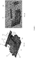
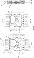
- a semiconductor package 100 includes a die pad 102, a plurality of electrically conductive leads 104, a semiconductor die 106, an electrically conductive interconnect clip 108, and a thermally conductive heat spreader 110.
- Figures 1A, 1B , 1C, 1D show a partial assembly of the package.
- Figure 1E shows a completed semiconductor package 100 which includes an electrically insulating encapsulant body 112.
- the encapsulant body 112 includes an electrically insulating encapsulant material, e.g., ceramic, epoxy material, thermosetting plastic, etc.
- the encapsulant material is formed such that the semiconductor die 106 is encapsulated, and such that outer ends of the leads 104, a lower surface of the die pad 102 and an upper surface 138 of the heat spreader 110 are exposed from the encapsulant material.
- the semiconductor package 100 can be mated to a printed circuit board with the leads 104 providing I/O connectivity and the die pad 102 and heat spreader 110 providing dual side cooling of the mounted semiconductor package 100.
- the die pad 102 and the leads 104 include an electrically conductive material, e.g., a metal such as copper, aluminium, nickel, etc., and alloys thereof.
- the die pad 102 and the leads 104 may be provided from a common lead frame structure which is structured from a planar sheet metal.
- the die pad 102 includes a die attach surface 114, which is a substantially planar and conductive surface configured for the mounting of a semiconductor die 106 thereon.
- the leads include a first lead 116 that is separated from the die pad 102 by a lateral gap between a first edge side 118 of the die pad 102 and an interior end of the first lead 116. The first lead 116 is physically detached and laterally separated from the die pad 102.
- a connection surface 120 of the first lead 116 extends to the interior end of the first lead 116.
- the connection surface 120 of the first lead 116 is configured to accommodate an interconnection structure, e.g., a bond wire, a clip, etc..
- the connection surface 120 is vertically spaced apart from the die attach surface 114. This vertical separation is in a vertical direction that is perpendicular to the die attach surface 114.
- the first lead 116 is includes a plurality of discrete lead portions that are fused together by a common pad. More generally, the first lead 116 can include any number of leads, including a single lead.
- the leads 104 additionally include a second lead 122 that is separated from the die pad 102 by a lateral gap between the first edge side 118 of the die pad 102 and an interior end of the second lead 122 in a similar manner.
- the semiconductor die 106 is mounted on the die attach surface 114 of the die pad 102.
- the semiconductor die 106 can have a wide variety of device configurations, such as MOSFET (Metal Oxide Semiconductor Field Effect Transistor), IGBT (Insulated Gate Bipolar Transistor), JFET (Junction Field Effect Transistor), diode, etc.
- the semiconductor die 106 may include any of a wide variety of semiconductor materials including type IV semiconductors, e.g., silicon, silicon germanium, silicon carbide, etc., and type III-V semiconductors, e.g., gallium nitride, gallium arsenide, etc.
- the semiconductor die 106 may be configured as a vertical device that is configured to control a current flowing between opposite facing upper and lower surfaces, or a lateral device that is configured to control a current flowing parallel to a main surface.
- the semiconductor die 106 is configured as a discrete MOSFET device. More specifically, the semiconductor die 106 may be configured as a silicon carbide-based power MOSFET device that is rated to control voltages of at least 1200 V (volts).
- the semiconductor die 106 is mounted with a lower surface that faces the die pad 102 and an upper surface that faces away from the die pad 102.
- the semiconductor die 106 includes first and second terminals 124, 126 on the upper surface of the semiconductor die 102.
- the first terminal 124 may be load terminal, such as a source terminal, drain terminal, collector terminal, etc., to which the main voltage is applied across.
- the second terminal 126 may be a control terminal, such as a gate terminal, base terminal, etc., that is configured to control a conductive state of the device.
- the semiconductor die 106 may additionally include a third terminal (not shown) on the rear surface.
- the third terminal may be another load terminal, such as a source terminal, drain terminal, collector terminal, etc., to which the main voltage is applied across.
- the semiconductor die 106 is a power MOSFET
- the first terminal 124 is a gate terminal
- the second terminal 126 is a source terminal
- the third terminal is a drain terminal.
- Each of these terminals may be implemented by electrically conductive bond pads disposed on the surfaces of the semiconductor die 106.
- the third terminal may be electrically connected to the die pad 102 by a conductive adhesive, e.g., solder, sinter, conductive glue, etc.
- the interconnect clip 108 includes an electrically conductive material, e.g., a metal such as copper, aluminium, nickel, etc., and alloys thereof.
- the interconnect clip 108 can be provided from a planar sheet metal and formed to include any of the geometric features described herein by metal processing techniques such as punching, stamping, bending, etc.
- the interconnect clip 108 includes a first planar section 128, a second planar section 130, and a third planar section 132.
- the first, second and third planar sections 128, 130, 132 may be part of a continuous and substantially uniform thickness structure, with each of the first, second and third planar sections 128, 130, 132 having a substantially identical thickness between opposite facing upper and lower surfaces.
- the first planar section 128 is parallel to and vertically offset from the third planar section 132. This vertical offset corresponds to the offset distance between the die attach surface 114 and the connection surface 120 of the first lead 116.
- the second planar section 130 vertically extends from the first planar section 128 towards the first lead 116.
- a first transitional bend 134 is disposed between the first and second planar sections 130, 132.
- a second transitional bend 136 is disposed between the second and third planar sections 130, 132. These transitional bends are locations of the interconnect clip 108 wherein the plane of the interconnect clip 108 changes direction.
- the first and second transitional bends 134, 136 form acute angled intersections between two planes. More generally, the first and second transitional bends 134, 136 may have curved or more gradual geometries.
- the angle of inclination between the second planar section 130 and the first planar and/or third planar section 132 may vary from gently sloped, e.g., 30 degrees, to steep, e.g., 90 degrees.
- the interconnect clip 108 electrically connects the first terminal 124 to the first lead 116.
- the interconnect clip 108 is mounted in the assembly with the first planar section 128 being flush against the upper surface of the semiconductor die 106 and third planar section 132 being flush against the connection surface 120 of the first lead 116. Electrical contact may be achieved by direct contact or by providing a conductive intermediary, e.g., solder, sinter, adhesive, etc., between the interconnect clip 108 and the first terminal 124 and/or the first lead 116.
- a conductive intermediary e.g., solder, sinter, adhesive, etc.
- the heat spreader 110 is a discrete piece of thermally conductive material.
- the heat spreader 110 can include a metal, such as copper, aluminium, etc., or alloys thereof.
- the heat spreader 110 is a continuous volume of thermally conductive material, meaning that no openings are cavities are contained within the heat spreader 110.
- the heat spreader 110 is mounted on an upper surface of the interconnect clip 108. This may be effectuated by a thermally conductive adhesive, e.g., solder, sinter, conductive glue, etc, provided between the heat spreader 110 and the heat spreader 110.
- a thermally conductive adhesive e.g., solder, sinter, conductive glue, etc
- the heat spreader 110 includes a substantially planar upper surface 138.
- this upper surface 138 of the heat spreader 110 may be exposed from the encapsulant 112 so as to provide an interface for connection to a heat sink.
- the first transitional bend 134 of the interconnect clip 108 is disposed in the lateral gap between the first edge side 118 of the die pad 102 and the interior end of the first lead 116. Hence, the first transitional bend 134 is laterally outside of the perimeter of the die pad 102.
- This configuration differs from conventional vertically offset clip designs wherein the angled transition occurs directly over the chip.
- a lateral distance between the first transitional bend 134 and the first edge side 118 of the die pad 102 is at least 50% of an overall lateral distance of the lateral gap, and may be more than 60%, more than 70%, more than 80%, more than 90%, etc., in various embodiments.
- the semiconductor die 106 includes a first outer edge 140 that faces the first lead 116, a second outer edge 142 opposite the first outer edge 140, and third and fourth outer edges 144, 146 each extending between the first and second outer edges 140, 142. These outer edges 140, 142, 144 and 146 form an outer perimeter of the semiconductor die 106.
- a portion of the upper surface of the semiconductor die 106 is covered by the interconnect clip 108.
- Another portion of the upper surface of the semiconductor die 106 is exposed from the interconnect clip 108. This exposed portion of the upper surface extends to the third outer edge 142 of the semiconductor die 106 and includes the second terminal 126.
- An electrically conductive bond wire 146 that electrically connects the second terminal 126 to the second lead 122 extends directly over the exposed portion of the upper surface.
- the heat spreader 110 includes a plurality of edge faces that form an outer perimeter of the heat spreader 110.
- the heat spreader 110 is arranged in a partially overlapping configuration with the semiconductor die 106 and with the interconnect clip 108. That is, the heat spreader 110 covers a portion of the interconnect clip 108.
- the heat spreader 110 laterally extends past the first outer edge 140 side of the semiconductor die 106. That is, the heat spreader 110 expands past the semiconductor die 106 in a first lateral direction 148 that is parallel to the current flow direction between the first terminal 124 and the first lead 116.
- the heat spreader 110 has a greater area than the semiconductor die 106.
- the heat spreader 110 may have an area that is twice as large as the semiconductor die 106. This means that the outer periphery of the heat spreader 110 as formed by the edge faces of the heat spreader 110 occupies a larger two-dimensional space than an outer periphery of the semiconductor die 106 as formed by the outer edges of the semiconductor die 106. If the heat spreader 110 has a multi-thickness configuration (e.g., as disclosed in below embodiments), the outer periphery of the heat spreader 110 refers to the outer periphery of the thickness region with the largest area.
- the large area of the heat spreader 110 is attributable to the geometric features of the interconnect clip 108, the heat spreader 110, or both. Specifically, by locating the first transitional bend 134 of the interconnect clip 108 in the lateral gap between the first edge side 118 of the die pad 102 and the first lead 116, the heat spreader 110 can be extended in the first lateral direction 148. Meanwhile, the geometry of the heat spreader 110 is tailored to allow the heat spreader 110 to extend past the third and/or fourth outer edges 142, 144 of the semiconductor die 106 in a second lateral direction 150 that is perpendicular to the first lateral direction 148, while simultaneously accommodating a bond wire. Various examples of these geometries are illustrated in the embodiments discussed below.
- the outer perimeter of the heat spreader 110 has a polygon shape.
- a polygon shape describes an enclosed geometry made up of at least five linear spans with an angled intersection between each span. In other words, a polygon is more complex than a rectangle.
- Examples of polygon geometries include U-shaped geometries, C-shaped geometries, otherwise rectangular geometries with notches in one side, and geometries that include obtuse angles. This configuration allows the heat spreader 110 to expand in different directions while simultaneously accommodating the bond wire.
- the polygon-shaped heat spreader 110 of Fig. 1 includes a side with three linear spans, with one of the linear spans being angled relative to the other two. This allows the heat spreader 110 to laterally extend past the third outer edge 142 of the semiconductor die 106.
- the heat spreader 110 laterally extends past at least two of the first, second, third and fourth outer edges 140, 142, 144, 146. In this way, the effective cooling surface of the heat spreader 110 can be beneficially increased.
- Various configurations of the heat spreader 110 and/or interconnect clip 108 will be described in further below for achieving this expanded surface area.
- the heat spreader 110 includes first and second edge faces 152, 154 that form an angled intersection with one another.
- the first and second edge faces 152, 150 may intersect one another at an angle of between about 120 and 150 degrees.
- the second terminal 126 is laterally disposed between the first edge face 152 and the third outer edge 142 of the semiconductor die 106.
- the second edge face 154 laterally extends past the third outer edge 142 of the semiconductor die 106. In the depicted embodiment, the second edge face 154 extends directly over the third outer edge 142 of the semiconductor die 106.
- the second edge face 152 may cross the plane third outer edge 142 outside of the die footprint.
- the heat spreader 110 also extends past the second outer edge 142 of the semiconductor die 106. Hence, a large surface area of the heat spreader 110 is provided.
- the heat spreader 110 includes first, second and third edge faces 152, 154, 156.
- the second terminal 126 is laterally disposed between the first edge face 152 and the third outer edge 142 of the semiconductor die 106.
- the second and third edge faces 154, 156 each form substantially perpendicular angles with the first edge face.
- the heat spreader 110 includes a u-shaped notch formed by three edge faces which accommodates the connection of the bond wire 146. This u-shaped notch provides an exposed area for the bond wire 146 to enter and contact the first terminal 124.
- the heat spreader 110 laterally extends past all four outer edges 140, 142, 144 and 146 of the semiconductor die 106. Hence, a large surface area of the heat spreader 110 is provided.
- the heat spreader 110 includes a thicker portion 158 and a thinner portion 160.
- the thickness of each portion is a shortest distance between upper and lower surface of the interconnect clip 108.
- the multi-thickness configuration allows the heat spreader 110 to laterally expand past the semiconductor die 106 in both the first lateral direction 148 and the second lateral direction 150.
- the lower surface of the thicker portion 158 is flush against the upper surface of the interconnect clip 108.
- the thicker portion 158 forms a thermal interface with the interconnect clip 108.
- a lower surface of the thinner portion 160 laterally extends outward from the thinner portion 160 and is spaced apart from the interconnect clip 108 in the region immediately adjacent the thicker portion 158.
- This lateral expansion of the interconnect clip 108 provides a larger surface area for the mounting of a heat sink on top of the heat spreader 110.
- the thinner portion 160 of the heat spreader 110 includes a first wing 162 that laterally extends past the thicker section 158 in the first lateral direction 148.
- the first wing 162 may laterally extend past the first transitional bend 134.
- the first wing 162 extends past both of the first and second transitional bends 134, 136 and directly contacts an upper surface of the interconnect clip 108 in the third planar section 132.
- the thinner portion 160 includes a second wing 164 that laterally extends past the second outer edge 142 of the semiconductor die 106.
- the second wing 164 may have similar or identical thickness and length as the first wing 162.
- the second wing 162 may extend past a second edge side of the die pad 102 that is opposite from the first edge side 118.
- the multi-thickness concept is used to expand the upper area of the heat spreader 110 in multiple different lateral directions.
- the thinner portion 160 of the heat spreader 110 includes third and fourth wings 166, 168 which laterally extend past the semiconductor die 106 in the second lateral direction 150.
- the third wing 166 laterally extends past the third outer edge 142 of the semiconductor die 106 and the fourth wing 164 laterally extends past the fourth outer edge 144 of the semiconductor die 106.
- the bond wire 146 can enter an area that is below the third wing 166 and access the second terminal 126 of the semiconductor die 106.
- features such as oblique angles or notches in the edge faces of the heat spreader 110 are not needed to accommodate the bond wire.
- the third and fourth wings 166, 168 may also extend past the first outer edge 140 and past the first and second transitional bends 134, 136 in the first lateral direction 148, thus providing the benefit of the first wing 162 as previously described.
- the heat spreader 110 includes at least one chamfer 170 between at two edge faces.
- a chamfer refers to a structural feature that intersects with two edge surfaces thereby reducing the transitional angle between the two edge surfaces.
- the heat spreader 110 includes first, second, third and fourth edge faces 172, 174, 176 and 178, wherein the first and second edge faces 172, 174 are substantially perpendicular to one another, the second and third edge faces 174, 176 are substantially perpendicular to one another, and so forth.
- the chamfers 170 are formed by planar edge faces oriented at about 45 degrees relative to two perpendicular edge faces. More generally, the angle of the chamfer 170 may vary and/or the chamfer 170 may include a rounded transition.
- One benefit of the chamfer 170 is a reduction in thermal stress, due to differences in coefficient of thermal expansion of the encapsulant material, which cause expansion or contraction at high temperatures, e.g., from the manufacturing process or during operation.
- FIG. 8 an embodiment of the semiconductor package 100 with a polygon-shaped heat spreader 110 is depicted, according to an embodiment.
- the heat spreader 110 has the same two-dimensional geometry as the heat spreader 110 described with reference to Fig. 3 .
- an upper surface 138 of the heat spreader 110 that is opposite from the upper surface of the interconnect clip 108 is corrugated.
- the upper surface of the heat spreader 110 includes alternating peaks and valleys. As shown, the peaks and valleys are regularly spaced apart and are substantially rectangular shaped. More generally, the corrugation pattern may include non-regular and/or non-rectangular features.
- corrugation One benefit of the corrugation is enhanced adhesion to the encapsulant material (e.g., mold compound). Another benefit of the corrugation is increased surface area in comparison to a flat upper surface configuration. This increased surface area leads provides enhanced heat dissipation if, for instance, an external heat sink is not used in combination with the device. Put another way, the corrugation incorporates a kind of heat sink structure into the package itself.
- the encapsulant material e.g., mold compound
- the heat spreader 110 has the same two-dimensional outer geometry as the heat spreader 110 described with reference to Fig. 3 .
- the heat spreader 110 includes a number of perforations 180 that extend through opposite facing upper and lower surfaces of the heat spreader 110. As shown, the perforations 180 are disposed in a region of the heat spreader 110 that extend past the second outer edge 142 of the die. More generally, the perforations 180 can be disposed in any region that is outside of the perimeter of the semiconductor die 106. Moreover, the size, number and shape of the perforations 180 may vary.
- perforations 180 One benefit of the perforations 180 is enhanced adhesion to the encapsulant material 112 due to increased surface area contact with the encapsulant material. This enhanced adhesion provides mechanical stability for the heat spreader 110 such that it does not easily deviate from the intended mounting position.
- FIG. 10 an embodiment of the semiconductor package 100 with a polygon-shaped heat spreader 110 is depicted, according to an embodiment.
- both the interconnect clip 108 and the heat spreader 110 have a different configuration than the previously described embodiments.
- the interconnect clip 108 has a multi-thickness configuration, which includes a thicker portion 182 and a thinner portion 184.
- the heat spreader 110 is a substantially flat structure that is disposed over the thicker and thinner portion 160s.
- the thicker portion 184 of the interconnect clip 108 may have about the same areal footprint as the semiconductor die 106 (e.g., within +/-10%) and includes a lower surface that flush against the upper surface of the semiconductor die 106.
- the thinner portion 184 of the interconnect clip 108 laterally extends outward from the thicker portion 184 of the interconnect clip 108, and thus has a larger area than the semiconductor die 106.
- the thinner portion 184 of the interconnect clip 108 laterally extends over the first, second and fourth outer edges 140, 142 and 144 of the semiconductor die 106.
- a lower wing of the thinner portion 184 extends past the third outer edge 142 of the semiconductor die 106 outside of the die footprint.
- the multi-thickness interconnect clip 108 configuration represents an alternative way to expand the area of the heat spreader 110 in both the first and second lateral directions 148, 150.
- the thicker portion 182 of the interconnect clip 108 provides a mechanism for pulling heat away from the semiconductor die 106, while the substantially flat heat spreader 110 may have a large surface area to transfer this heat to an external heat sink apparatus.
- these package configurations include any package design wherein heat dissipation is desirable at the upper surface of the semiconductor die and/or wherein the semiconductor die includes at least one upward facing bond pad that requires electrical connection.
- Examples of these package configurations include leaded packages, leadless packages, chip carrier packages, surface mount packages, stacked die packages, molded packages, cavity packages, etc.
- substantially encompasses absolute conformity with the specified requirement as well as minor deviations from absolute conformity with the requirement due to manufacturing process variations, assembly, and other factors that may cause a deviation from the design goal. Provided that the deviation is within process tolerances so as to achieve practical conformity and the components described herein are able to function according to the application requirements, the term “substantially” encompasses any of these deviations.
- electrically connected directly electrically connected
- directly electrically connected describes a permanent low-impedance connection between electrically connected elements, for example a direct contact between the relevant elements or a low-impedance connection via a metal and/or a highly doped semiconductor.
Landscapes
- Lead Frames For Integrated Circuits (AREA)
- Physics & Mathematics (AREA)
- Geometry (AREA)
- Cooling Or The Like Of Semiconductors Or Solid State Devices (AREA)
Abstract
Description
- Embodiments of this invention generally relate to semiconductor packages and more particularly relate to cooling and interconnect features of semiconductor packages.
- Semiconductor packages are designed to provide connective compatibility between a semiconductor die and an external apparatus, such as a printed circuit board (PCB). Additionally, semiconductor packages are designed to protect a semiconductor die from potentially damaging environmental conditions, such as temperature variations, moisture, dust particles, etc. An important design consideration in many semiconductor packages is the cooling capability of the package. Many semiconductor dies generate a substantial amount of heat during typical operation. One example of such a device is a power semiconductor device that is rated to block substantially large voltages, e.g., voltages in excess of 200 volts, during normal operation. Cooling features are often provided in semiconductor packages to maintain the semiconductor die at safe temperature ranges during operation.
- Dual side cooling packages represent one package design for enhanced thermal dissipation capacity. A dual side cooling package includes a thermally conductive element that draws heat away from a bottom of the die towards a bottom side of the package and a second thermally conductive element that draws heat away from a top of the die towards a top side of the package.
- Metal clips are desirable as interconnect features in high power applications due to their large current carrying capability and low thermal resistance. However, the inclusion of a metal interconnect clip in a dual side cooling package creates geometric constraints that limit the placement of cooling features.
- A semiconductor package is disclosed. According to an embodiment, the semiconductor package comprises a die pad comprising a die attach surface, a first lead that is laterally separated from and vertically offset from the die pad, a semiconductor die that is mounted on the die attach surface and comprises a first terminal on an upper surface of the semiconductor die that faces away from the die pad, an interconnect clip that is electrically connected to the first terminal and to the first lead, and a heat spreader mounted on top of the interconnect clip. The interconnect clip comprises a first planar section that interfaces with the upper surface of the semiconductor die and extends past an outer edge side of the die pad. The heat spreader covers an area of the first planar section that is larger than an area of the semiconductor die. The heat spreader laterally extends past a first outer edge side of the die pad that faces the first lead.
- Separately or in combination, the interconnect clip comprises a second planar section that forms a first transitional bend with the first planar section and vertically extends towards the first lead, and the first transitional bend is disposed in a lateral gap between the first edge side of the die pad and an interior end of the first lead.
- Separately or in combination, the interconnect clip comprises a third planar section that forms a second transitional bend with the second planar section is flush against a connection surface of the first lead, and the first and third planar sections are substantially parallel to one another.
- Separately or in combination, the semiconductor die comprises a first outer edge that faces the first lead, a second outer edge opposite the first outer edge, and third and fourth outer edges each extending between the first and second outer edges, and wherein the heat spreader laterally extends past at least two of the first, second, third and fourth outer edges.
- Separately or in combination, the semiconductor die further comprises a second terminal on the upper surface of the semiconductor die, the semiconductor package further comprises a second lead that is separated from the die pad by a lateral gap between the first edge side of the die pad and an interior end of the second lead, and an electrically conductive bond wire that electrically connects the second terminal to the second lead, the bond wire extends directly over an exposed region of the upper surface of the semiconductor die, the exposed region being a region of the upper surface of the semiconductor die that includes the second terminal, extends to the third outer edge of the semiconductor die, and is exposed from the interconnect clip.
- Separately or in combination, the heat spreader comprises first and second edge faces that form an angled intersection with one another, the second terminal is laterally disposed between the first edge face and the third outer edge of the semiconductor die, and the second edge face laterally extends past the third outer edge of the semiconductor die.
- Separately or in combination, the heat spreader comprises a thicker portion and a thinner portion, a lower surface of the thicker portion is flush against the upper surface of the interconnect clip, and a lower surface of the thinner portion laterally extends outward from the thinner portion and is spaced apart from the interconnect clip.
- Separately or in combination, the thinner portion comprises a first wing that laterally extends past the first transitional bend.
- Separately or in combination, the thinner portion comprises a second wing that laterally extends past the second outer edge of the semiconductor die.
- Separately or in combination, the thinner portion comprises a third wing that laterally extends past the third outer edge of the semiconductor die, and wherein the third wing extends over the bond wire.
- Separately or in combination, the thinner portion comprises a fourth wing that laterally extends past the fourth outer edge of the semiconductor die.
- Separately or in combination, the heat spreader comprises at least one chamfer between two edge faces that are substantially perpendicular to one another.
- Separately or in combination, an upper surface of the heat spreader that is opposite from the upper surface of the interconnect clip is corrugated.
- Separately or in combination, the heat spreader comprises at least one perforation that extends through opposite facing upper and lower surfaces of the heat spreader.
- Separately or in combination, the interconnect clip comprises a thicker portion and a thinner portion, wherein a lower surface of the thicker portion of the interconnect clip is flush against the upper surface of the semiconductor die, and the thinner portion of the interconnect clip laterally extends outward from the thicker portion of the interconnect clip.
- Separately or in combination, the heat spreader is a substantially flat structure this is disposed directly on the thicker portion and the thinner portion.
- Separately or in combination, an outer perimeter of the heat spreader has a polygon shape.
- Separately or in combination, the outer perimeter of the heat spreader comprises an obtuse angle at an intersection between two edge faces, or a u-shaped notch formed by three edge faces.
- The elements of the drawings are not necessarily to scale relative to each other. Like reference numerals designate corresponding similar parts. The features of the various illustrated embodiments can be combined unless they exclude each other. Embodiments are depicted in the drawings and are detailed in the description which follows.
-
Figure 1 , which includesFigs. 1A, 1B ,1C, 1D and 1E , illustrates a semiconductor package with an expanded interconnect clip and heat spreader design, according to an embodiment.Fig. 1A and 1B each depict an isometric view of the semiconductor package before encapsulation.Fig. 1C depicts a planar view of the semiconductor package before encapsulation with the interconnect clip and without the heat spreader.Fig. 1D depicts a planar view of the semiconductor package before encapsulation with the interconnect clip and the heat spreader.Fig. 1E depicts a cross-sectional view of the semiconductor package after encapsulation with the interconnect clip and the heat spreader. -
Figure 2 , which includesFigs. 2A, 2B and 2C , illustrates a semiconductor package with an expanded interconnect clip and heat spreader design, according to an embodiment.Fig. 2A depicts a planar view of the semiconductor package before encapsulation with the interconnect clip and without the heat spreader.Fig. 2B depicts a planar view of the semiconductor package before encapsulation with the interconnect clip and the heat spreader.Fig. 2C depicts a cross-sectional view of the semiconductor package with the interconnect clip and the heat spreader. -
Figure 3 , which includesFigs. 3A, 3B and 3C , illustrates a semiconductor package with an expanded interconnect clip and heat spreader design, according to an embodiment.Fig. 3A depicts a planar view of the semiconductor package before encapsulation with the interconnect clip and without the heat spreader.Fig. 3B depicts a planar view of the semiconductor package before encapsulation with the interconnect clip and the heat spreader.Fig. 3C depicts a cross-sectional view of the semiconductor package with the interconnect clip and the heat spreader. -
Figure 4 , which includesFigs. 4A, 4B and 4C , illustrates a semiconductor package with an expanded interconnect clip and heat spreader design, according to an embodiment.Fig. 4A depicts a planar view of the semiconductor package before encapsulation with the interconnect clip and without the heat spreader.Fig. 4B depicts a planar view of the semiconductor package before encapsulation with the interconnect clip and the heat spreader.Fig. 4C depicts a cross-sectional view of the semiconductor package with the interconnect clip and the heat spreader. -
Figure 5 , which includesFigs. 5A, 5B and 5C , illustrates a semiconductor package with an expanded interconnect clip and heat spreader design, according to an embodiment.Fig. 5A depicts a planar view of the semiconductor package before encapsulation with the interconnect clip and without the heat spreader.Fig. 5B depicts a planar view of the semiconductor package before encapsulation with the interconnect clip and the heat spreader.Fig. 5C depicts a cross-sectional view of the semiconductor package with the interconnect clip and the heat spreader. -
Figure 6 , which includesFigs. 6A, 6B, 6C and 6D , illustrates a semiconductor package with an expanded interconnect clip and heat spreader design, according to an embodiment.Fig. 6A depicts a planar view of the semiconductor package before encapsulation with the interconnect clip and without the heat spreader.Fig. 6B depicts a planar view of the semiconductor package before encapsulation with the interconnect clip and the heat spreader.Fig. 6C depicts a cross-sectional view of the semiconductor package with the interconnect clip and the heat spreader in a second lateral direction that is perpendicular to the current flow direction.Fig. 6D depicts a cross-sectional view of the semiconductor package with the interconnect clip and the heat spreader in a first lateral direction that is parallel to the current flow direction. -
Figure 7 , which includesFigs. 7A, 7B and 7C , illustrates a semiconductor package with an expanded interconnect clip and heat spreader design, according to an embodiment.Fig. 7A depicts a planar view of the semiconductor package before encapsulation with the interconnect clip and without the heat spreader.Fig. 7B depicts a planar view of the semiconductor package before encapsulation with the interconnect clip and the heat spreader.Fig. 7C depicts a cross-sectional view of the semiconductor package with the interconnect clip and the heat spreader. -
Figure 8 , which includesFigs. 8A, 8B and 8C , illustrates a semiconductor package with an expanded interconnect clip and heat spreader design, according to an embodiment.Fig. 8A depicts a planar view of the semiconductor package before encapsulation with the interconnect clip and without the heat spreader.Fig. 8B depicts a planar view of the semiconductor package before encapsulation with the interconnect clip and the heat spreader.Fig. 8C depicts a cross-sectional view of the semiconductor package with the interconnect clip and the heat spreader. -
Figure 9 , which includesFigs. 9A, 9B and 9C , illustrates a semiconductor package with an expanded interconnect clip and heat spreader design, according to an embodiment.Fig. 9A depicts a planar view of the semiconductor package before encapsulation with the interconnect clip and without the heat spreader.Fig. 9B depicts a planar view of the semiconductor package before encapsulation with the interconnect clip and the heat spreader.Fig. 9C depicts a cross-sectional view of the semiconductor package with the interconnect clip and the heat spreader. -
Figure 10 , which includesFigs. 10A, 10B and 10C , illustrates a semiconductor package with an expanded interconnect clip and heat spreader design, according to an embodiment.Fig. 10A depicts a planar view of the semiconductor package before encapsulation with the interconnect clip and without the heat spreader.Fig. 10B depicts a planar view of the semiconductor package before encapsulation with the interconnect clip and the heat spreader.Fig. 10C depicts a cross-sectional view of the semiconductor package with the interconnect clip and the heat spreader. - Embodiments of a dual side cooling package with an advantageous interconnect clip and heat spreader configuration are described herein. The interconnect clip is designed to provide maximal surface area to accommodate the mounting of a large heat spreader thereon, while simultaneously providing electrical connectivity between a semiconductor die and a lead that is vertically offset from the semiconductor die. The interconnect clip includes a large planar section that mates with the semiconductor die and laterally extends past the die pad of the package. This large planar section can accommodate a heat spreader which also laterally extends past the die pad. In an embodiment, this arrangement is made possible by locating a transitional bend of the interconnect clip in a lateral gap between die pad and the first lead. The heat spreader is designed to expand past the semiconductor die and/or the die pad in multiple different directions. In embodiments, this is made possible by a geometric configuration of the heat spreader that is more complex than a simple cubic shape that is typical of conventional heat spreader designs. For example, the heat spreader can include one or more of an L-shaped geometry, a U-shaped geometry, a notch, etc. In another example, the heat spreader has a multi-thickness configuration so that an upper region of the heat spreader can expand past the die and the die pad. In either case, the heat spreader provides a large cooling surface area while simultaneously accommodating a bond wire connection to the semiconductor die. When combined in a single package, the interconnect clip and heat spreader allow for much greater cooling area of the heat spreader (e.g., at least twice as large as the semiconductor die), which beneficially improves thermal dissipation capability.
- Referring to
Figs. 1-2 , a semiconductor package 100 includes adie pad 102, a plurality of electrically conductive leads 104, asemiconductor die 106, an electricallyconductive interconnect clip 108, and a thermallyconductive heat spreader 110.Figures 1A, 1B ,1C, 1D show a partial assembly of the package.Figure 1E shows a completed semiconductor package 100 which includes an electrically insulatingencapsulant body 112. Theencapsulant body 112 includes an electrically insulating encapsulant material, e.g., ceramic, epoxy material, thermosetting plastic, etc. The encapsulant material is formed such that the semiconductor die 106 is encapsulated, and such that outer ends of theleads 104, a lower surface of thedie pad 102 and anupper surface 138 of theheat spreader 110 are exposed from the encapsulant material. In this way, the semiconductor package 100 can be mated to a printed circuit board with theleads 104 providing I/O connectivity and thedie pad 102 andheat spreader 110 providing dual side cooling of the mounted semiconductor package 100. - The
die pad 102 and theleads 104 include an electrically conductive material, e.g., a metal such as copper, aluminium, nickel, etc., and alloys thereof. Thedie pad 102 and theleads 104 may be provided from a common lead frame structure which is structured from a planar sheet metal. Thedie pad 102 includes a die attachsurface 114, which is a substantially planar and conductive surface configured for the mounting of asemiconductor die 106 thereon. The leads include afirst lead 116 that is separated from thedie pad 102 by a lateral gap between afirst edge side 118 of thedie pad 102 and an interior end of thefirst lead 116. Thefirst lead 116 is physically detached and laterally separated from thedie pad 102. Aconnection surface 120 of thefirst lead 116 extends to the interior end of thefirst lead 116. Theconnection surface 120 of thefirst lead 116 is configured to accommodate an interconnection structure, e.g., a bond wire, a clip, etc.. Theconnection surface 120 is vertically spaced apart from the die attachsurface 114. This vertical separation is in a vertical direction that is perpendicular to the die attachsurface 114. In the depicted embodiment, thefirst lead 116 is includes a plurality of discrete lead portions that are fused together by a common pad. More generally, thefirst lead 116 can include any number of leads, including a single lead. The leads 104 additionally include asecond lead 122 that is separated from thedie pad 102 by a lateral gap between thefirst edge side 118 of thedie pad 102 and an interior end of thesecond lead 122 in a similar manner. - The semiconductor die 106 is mounted on the die attach
surface 114 of thedie pad 102. Generally speaking, the semiconductor die 106 can have a wide variety of device configurations, such as MOSFET (Metal Oxide Semiconductor Field Effect Transistor), IGBT (Insulated Gate Bipolar Transistor), JFET (Junction Field Effect Transistor), diode, etc. Moreover, the semiconductor die 106 may include any of a wide variety of semiconductor materials including type IV semiconductors, e.g., silicon, silicon germanium, silicon carbide, etc., and type III-V semiconductors, e.g., gallium nitride, gallium arsenide, etc. Moreover, the semiconductor die 106 may be configured as a vertical device that is configured to control a current flowing between opposite facing upper and lower surfaces, or a lateral device that is configured to control a current flowing parallel to a main surface. - According to an embodiment, the semiconductor die 106 is configured as a discrete MOSFET device. More specifically, the semiconductor die 106 may be configured as a silicon carbide-based power MOSFET device that is rated to control voltages of at least 1200 V (volts).
- The semiconductor die 106 is mounted with a lower surface that faces the
die pad 102 and an upper surface that faces away from thedie pad 102. The semiconductor die 106 includes first andsecond terminals first terminal 124 may be load terminal, such as a source terminal, drain terminal, collector terminal, etc., to which the main voltage is applied across. Thesecond terminal 126 may be a control terminal, such as a gate terminal, base terminal, etc., that is configured to control a conductive state of the device. The semiconductor die 106 may additionally include a third terminal (not shown) on the rear surface. The third terminal may be another load terminal, such as a source terminal, drain terminal, collector terminal, etc., to which the main voltage is applied across. In one embodiment, the semiconductor die 106 is a power MOSFET, thefirst terminal 124 is a gate terminal, thesecond terminal 126 is a source terminal, and the third terminal is a drain terminal. Each of these terminals may be implemented by electrically conductive bond pads disposed on the surfaces of the semiconductor die 106. The third terminal may be electrically connected to thedie pad 102 by a conductive adhesive, e.g., solder, sinter, conductive glue, etc. - The
interconnect clip 108 includes an electrically conductive material, e.g., a metal such as copper, aluminium, nickel, etc., and alloys thereof. Theinterconnect clip 108 can be provided from a planar sheet metal and formed to include any of the geometric features described herein by metal processing techniques such as punching, stamping, bending, etc. - The
interconnect clip 108 includes a firstplanar section 128, a secondplanar section 130, and a thirdplanar section 132. The first, second and thirdplanar sections planar sections planar section 128 is parallel to and vertically offset from the thirdplanar section 132. This vertical offset corresponds to the offset distance between the die attachsurface 114 and theconnection surface 120 of thefirst lead 116. The secondplanar section 130 vertically extends from the firstplanar section 128 towards thefirst lead 116. - A first
transitional bend 134 is disposed between the first and secondplanar sections transitional bend 136 is disposed between the second and thirdplanar sections interconnect clip 108 wherein the plane of theinterconnect clip 108 changes direction. In the depicted embodiment, the first and secondtransitional bends transitional bends planar section 130 and the first planar and/or thirdplanar section 132 may vary from gently sloped, e.g., 30 degrees, to steep, e.g., 90 degrees. - The
interconnect clip 108 electrically connects thefirst terminal 124 to thefirst lead 116. To effectuate this connection, theinterconnect clip 108 is mounted in the assembly with the firstplanar section 128 being flush against the upper surface of the semiconductor die 106 and thirdplanar section 132 being flush against theconnection surface 120 of thefirst lead 116. Electrical contact may be achieved by direct contact or by providing a conductive intermediary, e.g., solder, sinter, adhesive, etc., between theinterconnect clip 108 and thefirst terminal 124 and/or thefirst lead 116. - The
heat spreader 110 is a discrete piece of thermally conductive material. For example, theheat spreader 110 can include a metal, such as copper, aluminium, etc., or alloys thereof. According to an embodiment, theheat spreader 110 is a continuous volume of thermally conductive material, meaning that no openings are cavities are contained within theheat spreader 110. Theheat spreader 110 is mounted on an upper surface of theinterconnect clip 108. This may be effectuated by a thermally conductive adhesive, e.g., solder, sinter, conductive glue, etc, provided between theheat spreader 110 and theheat spreader 110. During operation of the semiconductor die 106, theheat spreader 110 draws heat away from the semiconductor die 106 via theinterconnect clip 108. According to an embodiment, theheat spreader 110 includes a substantially planarupper surface 138. In a complete semiconductor package 100, thisupper surface 138 of theheat spreader 110 may be exposed from theencapsulant 112 so as to provide an interface for connection to a heat sink. - According to an embodiment, the first
transitional bend 134 of theinterconnect clip 108 is disposed in the lateral gap between thefirst edge side 118 of thedie pad 102 and the interior end of thefirst lead 116. Hence, the firsttransitional bend 134 is laterally outside of the perimeter of thedie pad 102. This configuration differs from conventional vertically offset clip designs wherein the angled transition occurs directly over the chip. In an embodiment that utilizes this concept, a lateral distance between the firsttransitional bend 134 and thefirst edge side 118 of thedie pad 102 is at least 50% of an overall lateral distance of the lateral gap, and may be more than 60%, more than 70%, more than 80%, more than 90%, etc., in various embodiments. - As shown in
Fig. 1C , the semiconductor die 106 includes a firstouter edge 140 that faces thefirst lead 116, a secondouter edge 142 opposite the firstouter edge 140, and third and fourthouter edges outer edges outer edges interconnect clip 108. Another portion of the upper surface of the semiconductor die 106 is exposed from theinterconnect clip 108. This exposed portion of the upper surface extends to the thirdouter edge 142 of the semiconductor die 106 and includes thesecond terminal 126. An electricallyconductive bond wire 146 that electrically connects thesecond terminal 126 to thesecond lead 122 extends directly over the exposed portion of the upper surface. - As shown in
Fig. 2D , theheat spreader 110 includes a plurality of edge faces that form an outer perimeter of theheat spreader 110. Theheat spreader 110 is arranged in a partially overlapping configuration with the semiconductor die 106 and with theinterconnect clip 108. That is, theheat spreader 110 covers a portion of theinterconnect clip 108. - The
heat spreader 110 laterally extends past the firstouter edge 140 side of the semiconductor die 106. That is, theheat spreader 110 expands past the semiconductor die 106 in a firstlateral direction 148 that is parallel to the current flow direction between thefirst terminal 124 and thefirst lead 116. - According to an embodiment, the
heat spreader 110 has a greater area than the semiconductor die 106. Specifically, theheat spreader 110 may have an area that is twice as large as the semiconductor die 106. This means that the outer periphery of theheat spreader 110 as formed by the edge faces of theheat spreader 110 occupies a larger two-dimensional space than an outer periphery of the semiconductor die 106 as formed by the outer edges of the semiconductor die 106. If theheat spreader 110 has a multi-thickness configuration (e.g., as disclosed in below embodiments), the outer periphery of theheat spreader 110 refers to the outer periphery of the thickness region with the largest area. - The large area of the
heat spreader 110 is attributable to the geometric features of theinterconnect clip 108, theheat spreader 110, or both. Specifically, by locating the firsttransitional bend 134 of theinterconnect clip 108 in the lateral gap between thefirst edge side 118 of thedie pad 102 and thefirst lead 116, theheat spreader 110 can be extended in the firstlateral direction 148. Meanwhile, the geometry of theheat spreader 110 is tailored to allow theheat spreader 110 to extend past the third and/or fourthouter edges lateral direction 150 that is perpendicular to the firstlateral direction 148, while simultaneously accommodating a bond wire. Various examples of these geometries are illustrated in the embodiments discussed below. - According to an embodiment, the outer perimeter of the
heat spreader 110 has a polygon shape. As used herein, a polygon shape describes an enclosed geometry made up of at least five linear spans with an angled intersection between each span. In other words, a polygon is more complex than a rectangle. Examples of polygon geometries include U-shaped geometries, C-shaped geometries, otherwise rectangular geometries with notches in one side, and geometries that include obtuse angles. This configuration allows theheat spreader 110 to expand in different directions while simultaneously accommodating the bond wire. The polygon-shapedheat spreader 110 ofFig. 1 includes a side with three linear spans, with one of the linear spans being angled relative to the other two. This allows theheat spreader 110 to laterally extend past the thirdouter edge 142 of the semiconductor die 106. - According to an embodiment, the
heat spreader 110 laterally extends past at least two of the first, second, third and fourthouter edges heat spreader 110 can be beneficially increased. Various configurations of theheat spreader 110 and/orinterconnect clip 108 will be described in further below for achieving this expanded surface area. - Referring to
Fig. 2 , an embodiment of the semiconductor package 100 with a polygon-shapedheat spreader 110 is depicted, according to an embodiment. In the embodiment ofFig. 3 , theheat spreader 110 includes first and second edge faces 152, 154 that form an angled intersection with one another. For example, the first and second edge faces 152, 150 may intersect one another at an angle of between about 120 and 150 degrees. Thesecond terminal 126 is laterally disposed between thefirst edge face 152 and the thirdouter edge 142 of the semiconductor die 106. Thesecond edge face 154 laterally extends past the thirdouter edge 142 of the semiconductor die 106. In the depicted embodiment, thesecond edge face 154 extends directly over the thirdouter edge 142 of the semiconductor die 106. Alternatively, thesecond edge face 152 may cross the plane thirdouter edge 142 outside of the die footprint. In the depicted embodiment, theheat spreader 110 also extends past the secondouter edge 142 of the semiconductor die 106. Hence, a large surface area of theheat spreader 110 is provided. - Referring to
Fig. 3 , an embodiment of the semiconductor package 100 with a polygon-shapedheat spreader 110 is depicted, according to an embodiment. In this embodiment, theheat spreader 110 includes first, second and third edge faces 152, 154, 156. Thesecond terminal 126 is laterally disposed between thefirst edge face 152 and the thirdouter edge 142 of the semiconductor die 106. The second and third edge faces 154, 156 each form substantially perpendicular angles with the first edge face. As a result, theheat spreader 110 includes a u-shaped notch formed by three edge faces which accommodates the connection of thebond wire 146. This u-shaped notch provides an exposed area for thebond wire 146 to enter and contact thefirst terminal 124. In this embodiment, theheat spreader 110 laterally extends past all fourouter edges heat spreader 110 is provided. - Referring to
Fig. 4 , an embodiment of the semiconductor package 100 with a polygon-shaped and multi-thickness configuredheat spreader 110 is depicted, according to an embodiment. Theheat spreader 110 includes athicker portion 158 and athinner portion 160. The thickness of each portion is a shortest distance between upper and lower surface of theinterconnect clip 108. The multi-thickness configuration allows theheat spreader 110 to laterally expand past the semiconductor die 106 in both the firstlateral direction 148 and the secondlateral direction 150. The lower surface of thethicker portion 158 is flush against the upper surface of theinterconnect clip 108. Thus, thethicker portion 158 forms a thermal interface with theinterconnect clip 108. Meanwhile, a lower surface of thethinner portion 160 laterally extends outward from thethinner portion 160 and is spaced apart from theinterconnect clip 108 in the region immediately adjacent thethicker portion 158. This lateral expansion of theinterconnect clip 108 provides a larger surface area for the mounting of a heat sink on top of theheat spreader 110. - In the embodiment of
Fig. 4 , thethinner portion 160 of theheat spreader 110 includes afirst wing 162 that laterally extends past thethicker section 158 in the firstlateral direction 148. Thefirst wing 162 may laterally extend past the firsttransitional bend 134. As shown, thefirst wing 162 extends past both of the first and secondtransitional bends interconnect clip 108 in the thirdplanar section 132. Hence, the multi-thickness configuration enables a large area for cooling and thermal coupling to a heat sink structure. - Referring to
Fig. 5 , an embodiment of the semiconductor package 100 with a polygon-shaped and multi-thickness configuredheat spreader 110 is depicted, according to an embodiment. In this embodiment, thethinner portion 160 includes asecond wing 164 that laterally extends past the secondouter edge 142 of the semiconductor die 106. Hence, the effective surface contact area for cooling is expanded further in the firstlateral direction 148. Thesecond wing 164 may have similar or identical thickness and length as thefirst wing 162. Optionally, thesecond wing 162 may extend past a second edge side of thedie pad 102 that is opposite from thefirst edge side 118. - Referring to
Fig. 6 , an embodiment of the semiconductor package 100 with a polygon-shaped and multi-thickness configuredheat spreader 110 is depicted, according to an embodiment. In this embodiment, the multi-thickness concept is used to expand the upper area of theheat spreader 110 in multiple different lateral directions. Specifically, thethinner portion 160 of theheat spreader 110 includes third andfourth wings lateral direction 150. As shown inFig. 6C , thethird wing 166 laterally extends past the thirdouter edge 142 of the semiconductor die 106 and thefourth wing 164 laterally extends past the fourthouter edge 144 of the semiconductor die 106. Moreover, due to the vertical separation between thethird wing 166 and the die attachsurface 114, thebond wire 146 can enter an area that is below thethird wing 166 and access thesecond terminal 126 of the semiconductor die 106. Hence, in comparison to the previous embodiments, features such as oblique angles or notches in the edge faces of theheat spreader 110 are not needed to accommodate the bond wire. As shown inFig. 6D , the third andfourth wings outer edge 140 and past the first and secondtransitional bends lateral direction 148, thus providing the benefit of thefirst wing 162 as previously described. - Referring to
Fig. 7 , an embodiment of the semiconductor package 100 with a polygon-shapedheat spreader 110 is depicted, according to an embodiment. In this embodiment, theheat spreader 110 includes at least onechamfer 170 between at two edge faces. A chamfer refers to a structural feature that intersects with two edge surfaces thereby reducing the transitional angle between the two edge surfaces. In this example, theheat spreader 110 includes first, second, third and fourth edge faces 172, 174, 176 and 178, wherein the first and second edge faces 172, 174 are substantially perpendicular to one another, the second and third edge faces 174, 176 are substantially perpendicular to one another, and so forth. Thechamfers 170 are formed by planar edge faces oriented at about 45 degrees relative to two perpendicular edge faces. More generally, the angle of thechamfer 170 may vary and/or thechamfer 170 may include a rounded transition. One benefit of thechamfer 170 is a reduction in thermal stress, due to differences in coefficient of thermal expansion of the encapsulant material, which cause expansion or contraction at high temperatures, e.g., from the manufacturing process or during operation. - Referring to
Fig. 8 , an embodiment of the semiconductor package 100 with a polygon-shapedheat spreader 110 is depicted, according to an embodiment. In this embodiment, theheat spreader 110 has the same two-dimensional geometry as theheat spreader 110 described with reference toFig. 3 . Additionally, anupper surface 138 of theheat spreader 110 that is opposite from the upper surface of theinterconnect clip 108 is corrugated. This means that the upper surface of theheat spreader 110 includes alternating peaks and valleys. As shown, the peaks and valleys are regularly spaced apart and are substantially rectangular shaped. More generally, the corrugation pattern may include non-regular and/or non-rectangular features. One benefit of the corrugation is enhanced adhesion to the encapsulant material (e.g., mold compound). Another benefit of the corrugation is increased surface area in comparison to a flat upper surface configuration. This increased surface area leads provides enhanced heat dissipation if, for instance, an external heat sink is not used in combination with the device. Put another way, the corrugation incorporates a kind of heat sink structure into the package itself. - Referring to
Fig. 9 , an embodiment of the semiconductor package 100 with a polygon-shapedheat spreader 110 is depicted, according to an embodiment. In this embodiment, theheat spreader 110 has the same two-dimensional outer geometry as theheat spreader 110 described with reference toFig. 3 . Additionally, theheat spreader 110 includes a number ofperforations 180 that extend through opposite facing upper and lower surfaces of theheat spreader 110. As shown, theperforations 180 are disposed in a region of theheat spreader 110 that extend past the secondouter edge 142 of the die. More generally, theperforations 180 can be disposed in any region that is outside of the perimeter of the semiconductor die 106. Moreover, the size, number and shape of theperforations 180 may vary. One benefit of theperforations 180 is enhanced adhesion to theencapsulant material 112 due to increased surface area contact with the encapsulant material. This enhanced adhesion provides mechanical stability for theheat spreader 110 such that it does not easily deviate from the intended mounting position. - Referring to
Fig. 10 , an embodiment of the semiconductor package 100 with a polygon-shapedheat spreader 110 is depicted, according to an embodiment. In the embodiment ofFig. 10 , both theinterconnect clip 108 and theheat spreader 110 have a different configuration than the previously described embodiments. Specifically, theinterconnect clip 108 has a multi-thickness configuration, which includes athicker portion 182 and athinner portion 184. Moreover, theheat spreader 110 is a substantially flat structure that is disposed over the thicker and thinner portion 160s. - The
thicker portion 184 of theinterconnect clip 108 may have about the same areal footprint as the semiconductor die 106 (e.g., within +/-10%) and includes a lower surface that flush against the upper surface of the semiconductor die 106. Thethinner portion 184 of theinterconnect clip 108 laterally extends outward from thethicker portion 184 of theinterconnect clip 108, and thus has a larger area than the semiconductor die 106. In the depicted example, thethinner portion 184 of theinterconnect clip 108 laterally extends over the first, second and fourthouter edges thinner portion 184 extends past the thirdouter edge 142 of the semiconductor die 106 outside of the die footprint. By elevating the plane of lateral expansion to a plane that is substantially coplanar with thefirst lead 116, themulti-thickness interconnect clip 108 configuration represents an alternative way to expand the area of theheat spreader 110 in both the first and secondlateral directions thicker portion 182 of theinterconnect clip 108 provides a mechanism for pulling heat away from the semiconductor die 106, while the substantiallyflat heat spreader 110 may have a large surface area to transfer this heat to an external heat sink apparatus. - The concepts described herein are applicable to a wide variety of package configurations. Generally speaking, these package configurations include any package design wherein heat dissipation is desirable at the upper surface of the semiconductor die and/or wherein the semiconductor die includes at least one upward facing bond pad that requires electrical connection. Examples of these package configurations include leaded packages, leadless packages, chip carrier packages, surface mount packages, stacked die packages, molded packages, cavity packages, etc.
- The term "substantially" as used herein encompasses absolute conformity with the specified requirement as well as minor deviations from absolute conformity with the requirement due to manufacturing process variations, assembly, and other factors that may cause a deviation from the design goal. Provided that the deviation is within process tolerances so as to achieve practical conformity and the components described herein are able to function according to the application requirements, the term "substantially" encompasses any of these deviations.
- The term "electrically connected," "directly electrically connected" and the like as used herein describes a permanent low-impedance connection between electrically connected elements, for example a direct contact between the relevant elements or a low-impedance connection via a metal and/or a highly doped semiconductor.
- Spatially relative terms such as "under," "below," "lower," "over," "upper" and the like, are used for ease of description to explain the positioning of one element relative to a second element. These terms are intended to encompass different orientations of the device in addition to different orientations than those depicted in the figures. Further, terms such as "first," "second," and the like, are also used to describe various elements, regions, sections, etc. and are also not intended to be limiting. Like terms refer to like elements throughout the description.
- As used herein, the terms "having," "containing," "including," "comprising" and the like are open-ended terms that indicate the presence of stated elements or features, but do not preclude additional elements or features. The articles "a," "an" and "the" are intended to include the plural as well as the singular, unless the context clearly indicates otherwise.
- With the above range of variations and applications in mind, it should be understood that the present invention is not limited by the foregoing description, nor is it limited by the accompanying drawings. Instead, the present invention is limited only by the following claims and their legal equivalents.
Claims (15)
- A semiconductor package, comprising:a die pad comprising a die attach surface;a first lead that is laterally separated from and vertically offset from the die pad;a semiconductor die that is mounted on the die attach surface and comprises a first terminal on an upper surface of the semiconductor die that faces away from the die pad;an interconnect clip that is electrically connected to the first terminal and to the first lead; anda heat spreader mounted on top of the interconnect clip,wherein the interconnect clip comprises a first planar section that interfaces with the upper surface of the semiconductor die and extends past an outer edge side of the die pad,wherein the heat spreader covers an area of the first planar section that is larger than an area of the semiconductor die, andwherein the heat spreader laterally extends past a first outer edge side of the die pad that faces the first lead.
- The semiconductor package of claim 1, wherein the interconnect clip comprises a second planar section that forms a first transitional bend with the first planar section and vertically extends towards the first lead, and wherein the first transitional bend is disposed in a lateral gap between the first edge side of the die pad and an interior end of the first lead.
- The semiconductor package of claim 2, wherein the interconnect clip comprises a third planar section that forms a second transitional bend with the second planar section is flush against a connection surface of the first lead, and wherein the first and third planar sections are substantially parallel to one another.
- The semiconductor package of claim 2, wherein the semiconductor die comprises a first outer edge that faces the first lead, a second outer edge opposite the first outer edge, and third and fourth outer edges each extending between the first and second outer edges, and wherein the heat spreader laterally extends past at least two of the first, second, third and fourth outer edges.
- The semiconductor package of claim 4, wherein the semiconductor die further comprises a second terminal on the upper surface of the semiconductor die, wherein the semiconductor package further comprises a second lead that is separated from the die pad by a lateral gap between the first edge side of the die pad and an interior end of the second lead, and an electrically conductive bond wire that electrically connects the second terminal to the second lead, wherein the bond wire extends directly over an exposed region of the upper surface of the semiconductor die, the exposed region being a region of the upper surface of the semiconductor die that includes the second terminal, extends to the third outer edge of the semiconductor die, and is exposed from the interconnect clip.
- The semiconductor package of claim 5, wherein the heat spreader comprises first and second edge faces that form an angled intersection with one another, wherein the second terminal is laterally disposed between the first edge face and the third outer edge of the semiconductor die, and wherein the second edge face laterally extends past the third outer edge of the semiconductor die.
- The semiconductor package of claim 5, wherein the heat spreader comprises a thicker portion and a thinner portion, wherein a lower surface of the thicker portion is flush against the upper surface of the interconnect clip, and wherein a lower surface of the thinner portion laterally extends outward from the thinner portion and is spaced apart from the interconnect clip.
- The semiconductor package of claim 7, wherein the thinner portion comprises a first wing that laterally extends past the first transitional bend.
- The semiconductor package of claim 8, wherein the thinner portion comprises a second wing that laterally extends past the second outer edge of the semiconductor die.
- The semiconductor package of claim 7, wherein the thinner portion comprises a third wing that laterally extends past the third outer edge of the semiconductor die, and wherein the third wing extends over the bond wire.
- The semiconductor package of claim 10, wherein the thinner portion comprises a fourth wing that laterally extends past the fourth outer edge of the semiconductor die.
- The semiconductor package of claim 2, wherein at least one of:the heat spreader comprises at least one chamfer between two edge faces that are substantially perpendicular to one another,an upper surface of the heat spreader that is opposite from the upper surface of the interconnect clip is corrugated, andthe heat spreader comprises at least one perforation that extends through opposite facing upper and lower surfaces of the heat spreader.
- The semiconductor package of claim 1, wherein the interconnect clip comprises a thicker portion and a thinner portion, wherein a lower surface of the thicker portion of the interconnect clip is flush against the upper surface of the semiconductor die, and wherein the thinner portion of the interconnect clip laterally extends outward from the thicker portion of the interconnect clip.
- The semiconductor package of claim 1, wherein an outer perimeter of the heat spreader has a polygon shape.
- The semiconductor package of claim 14, wherein the outer perimeter of the heat spreader comprises:an obtuse angle at an intersection between two edge faces; ora u-shaped notch formed by three edge faces.
Applications Claiming Priority (1)
| Application Number | Priority Date | Filing Date | Title |
|---|---|---|---|
| US16/700,361 US11600547B2 (en) | 2019-12-02 | 2019-12-02 | Semiconductor package with expanded heat spreader |
Publications (2)
| Publication Number | Publication Date |
|---|---|
| EP3832713A1 true EP3832713A1 (en) | 2021-06-09 |
| EP3832713B1 EP3832713B1 (en) | 2026-03-11 |
Family
ID=73646186
Family Applications (1)
| Application Number | Title | Priority Date | Filing Date |
|---|---|---|---|
| EP20210646.4A Active EP3832713B1 (en) | 2019-12-02 | 2020-11-30 | Semiconductor package with expanded heat spreader |
Country Status (3)
| Country | Link |
|---|---|
| US (1) | US11600547B2 (en) |
| EP (1) | EP3832713B1 (en) |
| CN (1) | CN112992815B (en) |
Families Citing this family (2)
| Publication number | Priority date | Publication date | Assignee | Title |
|---|---|---|---|---|
| US11848244B2 (en) * | 2021-09-30 | 2023-12-19 | Texas Instruments Incorporated | Leaded wafer chip scale packages |
| US11908771B2 (en) * | 2021-11-12 | 2024-02-20 | Infineon Technologies Ag | Power semiconductor device with dual heat dissipation structures |
Citations (6)
| Publication number | Priority date | Publication date | Assignee | Title |
|---|---|---|---|---|
| US20080054449A1 (en) * | 2006-08-31 | 2008-03-06 | Infineon Technologies Ag | Semiconductor component with cooling apparatus |
| US20100133670A1 (en) * | 2008-12-01 | 2010-06-03 | Kai Liu | Top-side Cooled Semiconductor Package with Stacked Interconnection Plates and Method |
| US20100176508A1 (en) * | 2009-01-12 | 2010-07-15 | Ciclon Semiconductor Device Corp. | Semiconductor device package and method of assembly thereof |
| US20150076674A1 (en) * | 2013-09-13 | 2015-03-19 | Kabushiki Kaisha Toshiba | Semiconductor device and method of manufacturing the same |
| KR20160001373U (en) * | 2016-03-18 | 2016-04-28 | 제엠제코(주) | Clip structure for semiconductor package and semiconductor package including the same |
| US20180240770A1 (en) * | 2016-01-19 | 2018-08-23 | Jmj Korea Co., Ltd. | Clip-bonded semiconductor chip package using metal bumps and method for manufacturing the package |
Family Cites Families (15)
| Publication number | Priority date | Publication date | Assignee | Title |
|---|---|---|---|---|
| US6008991A (en) * | 1993-12-20 | 1999-12-28 | Lsi Logic Corporation | Electronic system including packaged integrated circuits with heat spreading standoff support members |
| US6547597B2 (en) * | 2001-07-10 | 2003-04-15 | Littelfuse, Inc. | Apparatus and method for incorporating surface mount components into connectors |
| JP2005191367A (en) * | 2003-12-26 | 2005-07-14 | Renesas Technology Corp | Semiconductor device and manufacturing method thereof |
| JP4628687B2 (en) * | 2004-03-09 | 2011-02-09 | ルネサスエレクトロニクス株式会社 | Semiconductor device |
| US7786555B2 (en) * | 2005-10-20 | 2010-08-31 | Diodes, Incorporated | Semiconductor devices with multiple heat sinks |
| US8062932B2 (en) * | 2008-12-01 | 2011-11-22 | Alpha & Omega Semiconductor, Inc. | Compact semiconductor package with integrated bypass capacitor and method |
| US20100164078A1 (en) * | 2008-12-31 | 2010-07-01 | Ruben Madrid | Package assembly for semiconductor devices |
| JP2010262973A (en) * | 2009-04-30 | 2010-11-18 | Renesas Electronics Corp | Semiconductor device |
| CN101651389B (en) * | 2009-06-29 | 2012-06-20 | 天津市天发重型水电设备制造有限公司 | Intrabundle gelling and compressing processing method for large high-voltage motor strip coil bar |
| DE112013007426B4 (en) * | 2013-09-11 | 2024-03-28 | Mitsubishi Electric Corporation | Semiconductor device and manufacturing method thereof |
| JP2015142072A (en) * | 2014-01-30 | 2015-08-03 | 株式会社東芝 | semiconductor device |
| US20170047274A1 (en) * | 2015-08-12 | 2017-02-16 | Texas Instruments Incorporated | Double Side Heat Dissipation for Silicon Chip Package |
| US10727163B2 (en) * | 2016-07-26 | 2020-07-28 | Mitsubishi Electric Corporation | Semiconductor device |
| US10840164B2 (en) | 2018-05-18 | 2020-11-17 | Infineon Technologies Ag | Wire bonded package with single piece exposed heat slug and leads |
| US11088046B2 (en) * | 2018-06-25 | 2021-08-10 | Semiconductor Components Industries, Llc | Semiconductor device package with clip interconnect and dual side cooling |
-
2019
- 2019-12-02 US US16/700,361 patent/US11600547B2/en active Active
-
2020
- 2020-11-20 CN CN202011307640.9A patent/CN112992815B/en active Active
- 2020-11-30 EP EP20210646.4A patent/EP3832713B1/en active Active
Patent Citations (6)
| Publication number | Priority date | Publication date | Assignee | Title |
|---|---|---|---|---|
| US20080054449A1 (en) * | 2006-08-31 | 2008-03-06 | Infineon Technologies Ag | Semiconductor component with cooling apparatus |
| US20100133670A1 (en) * | 2008-12-01 | 2010-06-03 | Kai Liu | Top-side Cooled Semiconductor Package with Stacked Interconnection Plates and Method |
| US20100176508A1 (en) * | 2009-01-12 | 2010-07-15 | Ciclon Semiconductor Device Corp. | Semiconductor device package and method of assembly thereof |
| US20150076674A1 (en) * | 2013-09-13 | 2015-03-19 | Kabushiki Kaisha Toshiba | Semiconductor device and method of manufacturing the same |
| US20180240770A1 (en) * | 2016-01-19 | 2018-08-23 | Jmj Korea Co., Ltd. | Clip-bonded semiconductor chip package using metal bumps and method for manufacturing the package |
| KR20160001373U (en) * | 2016-03-18 | 2016-04-28 | 제엠제코(주) | Clip structure for semiconductor package and semiconductor package including the same |
Also Published As
| Publication number | Publication date |
|---|---|
| CN112992815A (en) | 2021-06-18 |
| US11600547B2 (en) | 2023-03-07 |
| US20210166988A1 (en) | 2021-06-03 |
| CN112992815B (en) | 2026-02-03 |
| EP3832713B1 (en) | 2026-03-11 |
Similar Documents
| Publication | Publication Date | Title |
|---|---|---|
| US6330158B1 (en) | Semiconductor package having heat sinks and method of fabrication | |
| US11075185B2 (en) | Semiconductor package with multi-level conductive clip for top side cooling | |
| CN110504235B (en) | Wire bond package with monolithically exposed heatsink and leads | |
| CN108155172B (en) | Integrated circuit package | |
| US20220157686A1 (en) | Molded semiconductor package with dual integrated heat spreaders | |
| EP3832713B1 (en) | Semiconductor package with expanded heat spreader | |
| CN114446916A (en) | Three level interconnect clip | |
| JP4899481B2 (en) | Manufacturing method of resin-encapsulated semiconductor device having a heat radiator exposed outside | |
| US8471370B2 (en) | Semiconductor element with semiconductor die and lead frames | |
| US10978380B2 (en) | Semiconductor package with multi-level conductive clip for top side cooling | |
| KR20230144969A (en) | Discrete power semiconductor package | |
| CN112447671B (en) | Interconnection fixture having sloped contact surface and raised bridge | |
| JP4530863B2 (en) | Resin-sealed semiconductor device | |
| US20180102300A1 (en) | Connectable Package Extender for Semiconductor Device Package | |
| US8053285B2 (en) | Thermally enhanced single inline package (SIP) | |
| US11069600B2 (en) | Semiconductor package with space efficient lead and die pad design | |
| CN116031222A (en) | Semiconductor package with blind via attachment to heat sink | |
| CN116403976A (en) | Semiconductor device | |
| JP4556732B2 (en) | Semiconductor device and manufacturing method thereof | |
| US20210074667A1 (en) | Interconnect Clip with Angled Contact Surface and Raised Bridge Technical Field | |
| US20250183131A1 (en) | Semiconductor device, electronic device, and method of manufacturing electronic device | |
| JP7602095B2 (en) | Enhanced cooling package with improved thermal management of electrical components | |
| JP2026075889A (en) | Semiconductor equipment | |
| CN120221528A (en) | Package with component-carrying intermediate structure and additional carrier with reference potential structure | |
| CN119786480A (en) | Package carrier with large backside area |
Legal Events
| Date | Code | Title | Description |
|---|---|---|---|
| PUAI | Public reference made under article 153(3) epc to a published international application that has entered the european phase |
Free format text: ORIGINAL CODE: 0009012 |
|
| STAA | Information on the status of an ep patent application or granted ep patent |
Free format text: STATUS: THE APPLICATION HAS BEEN PUBLISHED |
|
| AK | Designated contracting states |
Kind code of ref document: A1 Designated state(s): AL AT BE BG CH CY CZ DE DK EE ES FI FR GB GR HR HU IE IS IT LI LT LU LV MC MK MT NL NO PL PT RO RS SE SI SK SM TR |
|
| STAA | Information on the status of an ep patent application or granted ep patent |
Free format text: STATUS: REQUEST FOR EXAMINATION WAS MADE |
|
| 17P | Request for examination filed |
Effective date: 20211207 |
|
| RBV | Designated contracting states (corrected) |
Designated state(s): AL AT BE BG CH CY CZ DE DK EE ES FI FR GB GR HR HU IE IS IT LI LT LU LV MC MK MT NL NO PL PT RO RS SE SI SK SM TR |
|
| STAA | Information on the status of an ep patent application or granted ep patent |
Free format text: STATUS: EXAMINATION IS IN PROGRESS |
|
| 17Q | First examination report despatched |
Effective date: 20241204 |
|
| GRAP | Despatch of communication of intention to grant a patent |
Free format text: ORIGINAL CODE: EPIDOSNIGR1 |
|
| STAA | Information on the status of an ep patent application or granted ep patent |
Free format text: STATUS: GRANT OF PATENT IS INTENDED |
|
| INTG | Intention to grant announced |
Effective date: 20250514 |
|
| GRAJ | Information related to disapproval of communication of intention to grant by the applicant or resumption of examination proceedings by the epo deleted |
Free format text: ORIGINAL CODE: EPIDOSDIGR1 |
|
| STAA | Information on the status of an ep patent application or granted ep patent |
Free format text: STATUS: EXAMINATION IS IN PROGRESS |
|
| INTC | Intention to grant announced (deleted) | ||
| GRAP | Despatch of communication of intention to grant a patent |
Free format text: ORIGINAL CODE: EPIDOSNIGR1 |
|
| STAA | Information on the status of an ep patent application or granted ep patent |
Free format text: STATUS: GRANT OF PATENT IS INTENDED |
|
| INTG | Intention to grant announced |
Effective date: 20251112 |
|
| GRAS | Grant fee paid |
Free format text: ORIGINAL CODE: EPIDOSNIGR3 |
|
| GRAA | (expected) grant |
Free format text: ORIGINAL CODE: 0009210 |
|
| STAA | Information on the status of an ep patent application or granted ep patent |
Free format text: STATUS: THE PATENT HAS BEEN GRANTED |
|
| P01 | Opt-out of the competence of the unified patent court (upc) registered |
Free format text: CASE NUMBER: UPC_APP_0002190_3832713/2026 Effective date: 20260121 |
|
| AK | Designated contracting states |
Kind code of ref document: B1 Designated state(s): AL AT BE BG CH CY CZ DE DK EE ES FI FR GB GR HR HU IE IS IT LI LT LU LV MC MK MT NL NO PL PT RO RS SE SI SK SM TR |
|
| REG | Reference to a national code |
Ref country code: CH Ref legal event code: F10 Free format text: ST27 STATUS EVENT CODE: U-0-0-F10-F00 (AS PROVIDED BY THE NATIONAL OFFICE) Effective date: 20260311 Ref country code: GB Ref legal event code: FG4D |
|
| REG | Reference to a national code |
Ref country code: DE Ref legal event code: R096 Ref document number: 602020068340 Country of ref document: DE |
|
| REG | Reference to a national code |
Ref country code: IE Ref legal event code: FG4D |
|
| PG25 | Lapsed in a contracting state [announced via postgrant information from national office to epo] |
Ref country code: RS Free format text: LAPSE BECAUSE OF FAILURE TO SUBMIT A TRANSLATION OF THE DESCRIPTION OR TO PAY THE FEE WITHIN THE PRESCRIBED TIME-LIMIT Effective date: 20260611 |
|
| PG25 | Lapsed in a contracting state [announced via postgrant information from national office to epo] |
Ref country code: ES Free format text: LAPSE BECAUSE OF FAILURE TO SUBMIT A TRANSLATION OF THE DESCRIPTION OR TO PAY THE FEE WITHIN THE PRESCRIBED TIME-LIMIT Effective date: 20260311 |
|
| PG25 | Lapsed in a contracting state [announced via postgrant information from national office to epo] |
Ref country code: GR Free format text: LAPSE BECAUSE OF FAILURE TO SUBMIT A TRANSLATION OF THE DESCRIPTION OR TO PAY THE FEE WITHIN THE PRESCRIBED TIME-LIMIT Effective date: 20260612 |
|
| REG | Reference to a national code |
Ref country code: LT Ref legal event code: MG9D |
|
| PG25 | Lapsed in a contracting state [announced via postgrant information from national office to epo] |
Ref country code: LT Free format text: LAPSE BECAUSE OF FAILURE TO SUBMIT A TRANSLATION OF THE DESCRIPTION OR TO PAY THE FEE WITHIN THE PRESCRIBED TIME-LIMIT Effective date: 20260311 |
|
| PG25 | Lapsed in a contracting state [announced via postgrant information from national office to epo] |
Ref country code: NO Free format text: LAPSE BECAUSE OF FAILURE TO SUBMIT A TRANSLATION OF THE DESCRIPTION OR TO PAY THE FEE WITHIN THE PRESCRIBED TIME-LIMIT Effective date: 20260611 |
|
| PG25 | Lapsed in a contracting state [announced via postgrant information from national office to epo] |
Ref country code: SE Free format text: LAPSE BECAUSE OF FAILURE TO SUBMIT A TRANSLATION OF THE DESCRIPTION OR TO PAY THE FEE WITHIN THE PRESCRIBED TIME-LIMIT Effective date: 20260311 Ref country code: FI Free format text: LAPSE BECAUSE OF FAILURE TO SUBMIT A TRANSLATION OF THE DESCRIPTION OR TO PAY THE FEE WITHIN THE PRESCRIBED TIME-LIMIT Effective date: 20260311 |
|
| REG | Reference to a national code |
Ref country code: NL Ref legal event code: MP Effective date: 20260311 |
|
| PG25 | Lapsed in a contracting state [announced via postgrant information from national office to epo] |
Ref country code: HR Free format text: LAPSE BECAUSE OF FAILURE TO SUBMIT A TRANSLATION OF THE DESCRIPTION OR TO PAY THE FEE WITHIN THE PRESCRIBED TIME-LIMIT Effective date: 20260311 |
|
| PG25 | Lapsed in a contracting state [announced via postgrant information from national office to epo] |
Ref country code: LV Free format text: LAPSE BECAUSE OF FAILURE TO SUBMIT A TRANSLATION OF THE DESCRIPTION OR TO PAY THE FEE WITHIN THE PRESCRIBED TIME-LIMIT Effective date: 20260311 |
|
| PG25 | Lapsed in a contracting state [announced via postgrant information from national office to epo] |
Ref country code: BG Free format text: LAPSE BECAUSE OF FAILURE TO SUBMIT A TRANSLATION OF THE DESCRIPTION OR TO PAY THE FEE WITHIN THE PRESCRIBED TIME-LIMIT Effective date: 20260311 |