EP3832647A1 - Energy recovery in filamentary resistive memories - Google Patents
Energy recovery in filamentary resistive memories Download PDFInfo
- Publication number
- EP3832647A1 EP3832647A1 EP20210483.2A EP20210483A EP3832647A1 EP 3832647 A1 EP3832647 A1 EP 3832647A1 EP 20210483 A EP20210483 A EP 20210483A EP 3832647 A1 EP3832647 A1 EP 3832647A1
- Authority
- EP
- European Patent Office
- Prior art keywords
- resistive
- switching element
- electrodes
- memory
- level
- Prior art date
- Legal status (The legal status is an assumption and is not a legal conclusion. Google has not performed a legal analysis and makes no representation as to the accuracy of the status listed.)
- Pending
Links
- 230000015654 memory Effects 0.000 title claims abstract description 52
- 238000011084 recovery Methods 0.000 title description 27
- 238000004090 dissolution Methods 0.000 claims abstract description 21
- 238000004146 energy storage Methods 0.000 claims abstract description 16
- 239000012212 insulator Substances 0.000 claims abstract description 11
- 230000003213 activating effect Effects 0.000 claims abstract description 7
- 238000000034 method Methods 0.000 claims description 27
- 239000003990 capacitor Substances 0.000 claims description 15
- 230000008878 coupling Effects 0.000 claims description 6
- 238000010168 coupling process Methods 0.000 claims description 6
- 238000005859 coupling reaction Methods 0.000 claims description 6
- 230000009467 reduction Effects 0.000 description 18
- 239000002184 metal Substances 0.000 description 10
- 238000010586 diagram Methods 0.000 description 9
- 230000008569 process Effects 0.000 description 8
- 238000005516 engineering process Methods 0.000 description 7
- 230000014759 maintenance of location Effects 0.000 description 6
- 239000003792 electrolyte Substances 0.000 description 5
- VYPSYNLAJGMNEJ-UHFFFAOYSA-N Silicium dioxide Chemical compound O=[Si]=O VYPSYNLAJGMNEJ-UHFFFAOYSA-N 0.000 description 4
- 238000013500 data storage Methods 0.000 description 4
- 238000007599 discharging Methods 0.000 description 4
- 239000007787 solid Substances 0.000 description 4
- 230000008901 benefit Effects 0.000 description 3
- 150000001768 cations Chemical class 0.000 description 3
- 238000003306 harvesting Methods 0.000 description 3
- 230000001965 increasing effect Effects 0.000 description 3
- 239000000463 material Substances 0.000 description 3
- 238000003860 storage Methods 0.000 description 3
- 230000007704 transition Effects 0.000 description 3
- 229910002370 SrTiO3 Inorganic materials 0.000 description 2
- 229910052681 coesite Inorganic materials 0.000 description 2
- 229910052906 cristobalite Inorganic materials 0.000 description 2
- 238000001514 detection method Methods 0.000 description 2
- 230000000694 effects Effects 0.000 description 2
- 230000006870 function Effects 0.000 description 2
- 230000014509 gene expression Effects 0.000 description 2
- 230000001939 inductive effect Effects 0.000 description 2
- 230000003647 oxidation Effects 0.000 description 2
- 238000007254 oxidation reaction Methods 0.000 description 2
- 239000000377 silicon dioxide Substances 0.000 description 2
- 229910052682 stishovite Inorganic materials 0.000 description 2
- 229910052905 tridymite Inorganic materials 0.000 description 2
- TVEXGJYMHHTVKP-UHFFFAOYSA-N 6-oxabicyclo[3.2.1]oct-3-en-7-one Chemical compound C1C2C(=O)OC1C=CC2 TVEXGJYMHHTVKP-UHFFFAOYSA-N 0.000 description 1
- 238000013459 approach Methods 0.000 description 1
- 230000006399 behavior Effects 0.000 description 1
- 230000008859 change Effects 0.000 description 1
- 238000012512 characterization method Methods 0.000 description 1
- 238000006243 chemical reaction Methods 0.000 description 1
- 239000004020 conductor Substances 0.000 description 1
- 230000001351 cycling effect Effects 0.000 description 1
- 230000005684 electric field Effects 0.000 description 1
- 238000005323 electroforming Methods 0.000 description 1
- 238000005265 energy consumption Methods 0.000 description 1
- 238000010438 heat treatment Methods 0.000 description 1
- 230000010354 integration Effects 0.000 description 1
- 150000002500 ions Chemical class 0.000 description 1
- 238000004519 manufacturing process Methods 0.000 description 1
- 230000007246 mechanism Effects 0.000 description 1
- 229910021645 metal ion Inorganic materials 0.000 description 1
- 229910044991 metal oxide Inorganic materials 0.000 description 1
- 150000004706 metal oxides Chemical class 0.000 description 1
- 239000002245 particle Substances 0.000 description 1
- 230000000630 rising effect Effects 0.000 description 1
- 239000004065 semiconductor Substances 0.000 description 1
- PBCFLUZVCVVTBY-UHFFFAOYSA-N tantalum pentoxide Inorganic materials O=[Ta](=O)O[Ta](=O)=O PBCFLUZVCVVTBY-UHFFFAOYSA-N 0.000 description 1
- 230000005641 tunneling Effects 0.000 description 1
Images


Classifications
-
- G—PHYSICS
- G11—INFORMATION STORAGE
- G11C—STATIC STORES
- G11C13/00—Digital stores characterised by the use of storage elements not covered by groups G11C11/00, G11C23/00, or G11C25/00
- G11C13/0002—Digital stores characterised by the use of storage elements not covered by groups G11C11/00, G11C23/00, or G11C25/00 using resistive RAM [RRAM] elements
- G11C13/0007—Digital stores characterised by the use of storage elements not covered by groups G11C11/00, G11C23/00, or G11C25/00 using resistive RAM [RRAM] elements comprising metal oxide memory material, e.g. perovskites
-
- G—PHYSICS
- G11—INFORMATION STORAGE
- G11C—STATIC STORES
- G11C13/00—Digital stores characterised by the use of storage elements not covered by groups G11C11/00, G11C23/00, or G11C25/00
- G11C13/0002—Digital stores characterised by the use of storage elements not covered by groups G11C11/00, G11C23/00, or G11C25/00 using resistive RAM [RRAM] elements
- G11C13/0009—RRAM elements whose operation depends upon chemical change
- G11C13/0011—RRAM elements whose operation depends upon chemical change comprising conductive bridging RAM [CBRAM] or programming metallization cells [PMCs]
-
- G—PHYSICS
- G11—INFORMATION STORAGE
- G11C—STATIC STORES
- G11C13/00—Digital stores characterised by the use of storage elements not covered by groups G11C11/00, G11C23/00, or G11C25/00
- G11C13/0002—Digital stores characterised by the use of storage elements not covered by groups G11C11/00, G11C23/00, or G11C25/00 using resistive RAM [RRAM] elements
- G11C13/0021—Auxiliary circuits
- G11C13/0038—Power supply circuits
-
- G—PHYSICS
- G11—INFORMATION STORAGE
- G11C—STATIC STORES
- G11C13/00—Digital stores characterised by the use of storage elements not covered by groups G11C11/00, G11C23/00, or G11C25/00
- G11C13/0002—Digital stores characterised by the use of storage elements not covered by groups G11C11/00, G11C23/00, or G11C25/00 using resistive RAM [RRAM] elements
- G11C13/0021—Auxiliary circuits
- G11C13/0069—Writing or programming circuits or methods
-
- G—PHYSICS
- G11—INFORMATION STORAGE
- G11C—STATIC STORES
- G11C5/00—Details of stores covered by group G11C11/00
- G11C5/14—Power supply arrangements, e.g. power down, chip selection or deselection, layout of wirings or power grids, or multiple supply levels
-
- G—PHYSICS
- G11—INFORMATION STORAGE
- G11C—STATIC STORES
- G11C13/00—Digital stores characterised by the use of storage elements not covered by groups G11C11/00, G11C23/00, or G11C25/00
- G11C13/0002—Digital stores characterised by the use of storage elements not covered by groups G11C11/00, G11C23/00, or G11C25/00 using resistive RAM [RRAM] elements
- G11C13/0021—Auxiliary circuits
- G11C13/0069—Writing or programming circuits or methods
- G11C2013/009—Write using potential difference applied between cell electrodes
-
- G—PHYSICS
- G11—INFORMATION STORAGE
- G11C—STATIC STORES
- G11C2213/00—Indexing scheme relating to G11C13/00 for features not covered by this group
- G11C2213/70—Resistive array aspects
- G11C2213/79—Array wherein the access device being a transistor
Definitions
- the present disclosure relates generally to the field of resistive memories, and more particularly to a method and circuit for recovering energy in resistive-switching memories.
- Resistive random access memory is a well-known class of semiconductor memory technology that is based on the so-called “filamentary switching" effect.
- filamentary switching examples include OxRAM (Oxide Random Access Memory) and CBRAM (conductive bridging RAM). These technologies have advantages in terms of cost, CMOS fabrication process compatibility, and ease of integration.
- Memory elements of a filamentary switching RRAM often have a MIM (metal-insulator-metal) structure, the metal layers forming electrodes, which sandwich the insulator layer there-between.
- the memory element is initially in an initial resistive state (IRS), which is generally of high resistance.
- IFS initial resistive state
- a voltage above a certain threshold voltage is applied across the metal electrodes, a thin conductive filament is deposited across the insulator creating a conducting path, thereby causing a short circuit to occur between the two metal electrodes, and programming a low resistance state (LRS).
- a high resistance state (HRS) can then be programmed by applying a voltage of opposite polarity, causing the conductive filament to be dissolved.
- a drawback of the programming operation of RRAM memory elements is thus that it involves non-negligible power consumption.
- RRAM Recommendation RAM
- a memory comprising: a resistive-switching element having first and second electrodes separated by a layer of insulator; an energy storage component or load coupled to the resistive-switching element via a first switch; and a control circuit configured: to program the resistive-switching element to have a set state, wherein, in the set state, a filament forms a conducting path between the first and second electrodes; and, following a dissolution of the filament, to recover electrical energy, generated by the dissolution of the filament, from one of the first and second electrodes by activating the first switch.
- the energy storage component or load comprises: a capacitor; or an inductor; or a resistor; or any combination of two or three of the above.
- control circuit is configured to apply a biasing voltage of a first level and having a first polarity across the first and second electrodes in order to program the set state.
- control circuit is further configured to apply a biasing voltage of a second level, and having a second polarity opposite to the first polarity, across the first and second electrodes in order to dissolve the filament.
- control circuit is further configured to apply a biasing voltage of a third level, and having the second polarity, across the first and second electrodes prior to recovering the electrical energy, the third level having a greater absolute value than the second level.
- the third level is in the range -0.5 to -5 V, and for example in the range -1 to -3 V.
- the third level has an absolute value that is equal to or greater than a fourth level at which a current conducted by the resistive-switching element falls to zero.
- control circuit is further configured to apply a biasing voltage of a fifth level, and having the second polarity, across the first and second electrodes prior to recovering further energy, the fifth level having a greater absolute value than the third level.
- the memory comprises a second switch coupling the first electrode of the resistive-switching element to a biasing circuit, the first switch couples the first electrode of the resistive-switching element to an energy storage node, and the control circuit is configured to recover electrical energy from one of the first and second electrodes by deactivating the second switch and activating the first switch.
- the memory further comprises a third switch coupling the energy storage node to the load.
- the memory comprises an array formed of the resistive-switching element and a plurality of further resistive-switching elements having first and second electrodes.
- control circuit is further configured to recover electrical energy from one of the first and second electrodes of each of the further resistive-switching elements following a dissolution of the filament of each resistive-switching element.
- the memory further comprises a plurality of further control circuits for controlling the plurality of further resistive-switching elements.
- a method of programming a resistive-switching element having first and second electrodes comprising: programming, by a control circuit, the resistive-switching element to have a set state wherein, in the set state, a filament forms a conducting path between the first and second electrodes; and following a dissolution of the filament, recovering, from one of the first and second electrodes, electrical energy generated by the dissolution of the filament by activating a first switch, the first switch coupling the resistive-switching element to a load.
- programming the resistive-switching element to have the set state comprises applying, by the control circuit, a biasing voltage of a first level and having a first polarity across the first and second electrodes.
- the method further comprises applying, by the control circuit, a biasing voltage of a second level, and having a second polarity opposite to the first polarity, across the first and second electrodes in order to dissolve the filament.
- the method further comprises applying, by the control circuit, a biasing voltage of a third level, and having the second polarity, across the first and second electrodes prior to recovering the electrical energy, the third level having a greater absolute value than the second level.
- the third level is in the range -0.5 to -5 V, and for example in the range -1 to -3 V.
- FIG. 1 schematically illustrates an example of a resistive-switching element 100 that operates based on filamentary switching.
- the element 100 has a MIM structure comprising a layer of insulator (INSULATOR) 102 forming an electrolyte and sandwiched between a top metal electrode (METAL) 104 at a voltage V TE and a bottom metal electrode (METAL) 106 at a voltage V BE .
- the element 100 is capable of storing a bit of data under control of a biasing voltage V BIAS applied across its electrodes 104, 106.
- Figure 1 also illustrates a control circuit (CTRL) 108 configured, for example, to generate the biasing voltage V BIAS for applying across the electrodes of the element 100, for example based on input data D_WR to be written to the element.
- CTRL control circuit
- the control circuit 108 is also for example configured to recover electrical energy from one of the electrodes 104, 106 following a dissolution of the filament of the element 100, as will be described in more detail below.
- Figure 2 illustrates an example of forming, set and reset programming phases of the resistive-switching element 100 of Figure 1 .
- the element 100 Prior to any programming operation, the element 100 is for example in an initial resistive state (IRS).
- a process known as forming or electroforming (FORMING) involves applying a biasing voltage V BIAS across the electrodes of the element 100 to cause a transition from the IRS state to a low resistance state (LRS).
- the element 100 can for example be made to toggle between the low resistance state and a high resistance state (HRS), these states being respectively associated with distinguishable low and high resistance values in order to provide binary data storage.
- HRS high resistance state
- a transition from the LRS state to the HRS state is generally referred to as a reset operation (RESET), and the HRS state is generally considered to correspond to a logic "0" state or OFF state.
- a transition from the HRS state to the LRS state is generally referred to as a set operation (SET), and the LRS state is generally considered to correspond to a logic "1" state or ON state.
- Transitioning from the IRS or HRS state to the LRS state involves applying a biasing voltage V BIAS across the resistive-switching element 100 in order to form a filament 202 across the insulating layer 102.
- This filament forms a conducting path between the electrodes 104, 106, thereby short circuiting the electrodes.
- Transitioning from the LRS state to the HRS state involves at least partially dissolving the filament 202 such that there is no longer a short circuit between the electrodes 104, 106 of the device.
- the filament may self-dissolve, while in other cases, the filament is caused to dissolve by applying a biasing voltage V BIAS of opposite polarity to the one used for the SET operation.
- conductive bridge RAM is described in more detail in the publication by D.Jana et al. entitled “Conductive-bridging random access memory: challenges and opportunity for 3D architecture", Nanoscale Research Letters, 2015 .
- Oxide Random Access Memory is for example described in more detail in the publication by H.S.Philip Wong et al. entitled “Metal-Oxide RRAM", Proceedings of the IEEE, 2012 .
- the contents of these two publications is for example incorporated herein by reference to the extent permitted by the law.
- Figure 3 schematically represents non-volatile and volatile programming cycles of a resistive-switching element such as the element 100 of Figure 1 .
- a sequence A in Figure 3 represents a non-volatile programming cycle, which for example involves a non-volatile set operation (NON-VOLATILE SET) creating a filament 302 between the electrodes of the element.
- the operation is considered non-volatile because enough power is applied to the element during the set process that the resulting filament is relatively thick, and therefore is not dissolved in the absence of an external bias.
- the non-volatile LRS state is maintained for a relatively long duration, such as months or years.
- the LRS state is for example read during a read operation (READ), involving detecting the low resistance state of the element and outputting the associated logic level, which is for example a logic "1".
- READ read operation
- a reset operation When the element is next to be programmed at the high resistance state, a reset operation (RESET) is applied by biasing the element with a biasing voltage V BIAS of opposite polarity to the one used during the set operation.
- V BIAS biasing voltage
- the result is for example that only a portion 304 of the filament 302 remains, and thus there is a relatively high resistance between the electrodes of the element.
- This reset state is always non-volatile in that the filament will not be reformed in the absence of an appropriate biasing voltage V BIAS applied across the electrodes.
- the HRS state is for example read during a further read operation (READ), involving detecting the high resistance state of the element and outputting the associated logic level, which is for example a logic "0".
- READ further read operation
- a sequence B in Figure 3 represents a volatile programming cycle, which for example involves a volatile set operation (VOLATILE SET) creating a filament 306 between the electrodes of the element.
- the operation is considered volatile because relatively low power is applied to the element during the set process and so the resulting filament 306 is relatively thin, and will tend to self-dissolve after a limited time window, which will be referred to herein as a retention time window.
- the volatile LRS state is maintained for a relatively short duration of between 1 ⁇ s and several days, and in some embodiments of two days at most.
- the LRS state is for example read during a read operation (READ), involving detecting the low resistance state of the element and outputting the associated logic level, which is for example a logic "1".
- a DRAM (dynamic RAM) operation is applied according to which elements programmed to have the LRS state are refreshed by a new volatile set if they are to store their data beyond the end of the retention time window.
- the read operation is for example part of a refresh operation of the element, and after reading the LRS state, this state is reprogrammed in order to extend the data storage duration.
- a self reset event for example occurs at the end of the retention time window.
- the result of this self reset event is for example that only a portion 308 of the filament 306 remains, and thus there is a relatively high resistance between the electrodes of the element.
- the HRS state is for example read during a further read operation (READ), involving detecting the high resistance state of the element and outputting the associated logic level, which is for example a logic "0".
- READ further read operation
- the conductive particles of the filament may have entirely dissolved and dispersed in the insulator.
- the following table provides approximate measured voltages V CELL for CBRAM and OxRAM elements having different materials for the top electrode (TE), the insulator (INSUL) and the bottom electrode (BE).
- the voltage V CELL is a voltage measured across the cells electrodes in open circuit conditions after "charging".
- the present inventors propose a method and circuit for harvesting the energy resulting from this electromotive force, as will now be described with reference to Figures 4 to 14 .
- Figure 4 is a graph representing an example of operating voltage V BIAS and current ranges for a memory mode and an energy recuperation mode of a resistive-switching element according to an example embodiment of the present disclosure.
- the memory mode corresponds to the use of the programming cycles of the resistive-switching element for data storage, as described above in relation with Figure 3 .
- the memory mode for example involves applying biasing voltages V BIAS across the electrodes of the resistive-switching element in the range of around -3 to 3 V, with currents anywhere in the range of 1 fA to 1 mA, and preferably of 1 ⁇ A to 100 ⁇ A.
- the energy recuperation mode corresponds to the presence, while not in the set state, of a voltage across the electrodes of the resistive-switching element, which can be harvested.
- the energy recuperation mode is compatible with voltages in the range from -8 V up to the voltage at which the filament is formed, which is for example at around 1 V.
- the present inventors have found that, as long as the filament is not formed, the energy recuperation mode is, however, more generally compatible with biasing voltages V BIAS in the range from around -10 to 10 V, and for example in the range from -5 to 5 V, and with currents anywhere in the range of 1 fA to 1 mA, and preferably of 1 ⁇ A to 100 ⁇ A.
- biasing voltage V BIAS may be brought below -3 V during the energy recovery.
- the voltage is varied in the range between -5 and 1 V.
- Figure 5 is a graph representing a current and biasing voltage V BIAS during a programming and energy recovery cycle of a resistive-switching element according to an example embodiment of the present disclosure. This graph was obtained by a technique of quasi-static memory characterization involving biasing the resistive-switching element with a ramping voltage source corresponding to the voltage V BIAS across the two electrodes of the element, while measuring the current across the electrodes.
- the biasing voltage V BIAS is swept from a negative voltage of relatively high absolute value to a positive voltage of relatively high absolute value, and back again, in order to characterize the behavior of the element during a programming cycle.
- the biasing voltage V BIAS starts at a point (1) at around -2 V.
- the resistive-switching element is for example in the IRS or HRS state. In this state, the resistive-switching element undergoes no change by the external bias, as substantially no ion is being produced, and no electromotive force can thus arise.
- the biasing voltage V BIAS across the electrodes of the element is then increased, for example by a voltage ramp.
- a certain positive voltage level equal for example to between 0.1 and 0.5 V
- the interface between the top electrode and electrolyte layer starts to undergo oxidation, and metal cations are released inside the electrolyte.
- An electromotive force starts to arise mainly due to the ionic gradient present inside the electrolyte layer. As the voltage increases further, the oxidation is enhanced and more metal ions are produced and consequently either diffuse or are swept by the electric field to the bottom electrode, where they are reduced, and lose their charged state.
- the biasing voltage V BIAS is not increased much higher than the voltage V_SET, and for example not more than around V_SET+0.5 V, equal to around 1 V in the example Figure 5 .
- the current has a trough 504 when the biasing voltage V BIAS reaches a level V_Imin, equal to around -0.4 V in the example of Figure 5 .
- the voltage range from V_Imin to a little over V_SET, for example V_SET plus between 1 and 10 percent, represented by a dashed rectangle 506 in Figure 5 corresponds for example to the memory programming voltage range.
- a more negative voltage range from V_Imin to a discharged level V_DISCHG at (5), and represented by a shaded rectangle 508 in Figure 5 is associated with a further current peak 510, corresponding to a peak electromotive force. This peak corresponds to a reduction peak, and the voltage range 508 from V_Imin to V_DISCHG corresponds to a deep reduction regime.
- an electromotive force is obtained by stopping the voltage in the shaded area 508, in other words by reducing the voltage to a final level within the range V_Imin to V_DISCHG, and then placing the resistive-switching element in open circuit.
- the final voltage level is for example determined during a calibration step in order to achieve a relatively high, or maximum, electromotive force Vemf.
- the voltage V_DISCHG is equal to around -1.3 V.
- the present inventors have found that the closer the reset voltage gets to the level V_DISCHG corresponding to the negative limit of the deep reduction regime, the greater the energy that can be recovered. Indeed, the maximum charge that can be generated is met when this point is reached, as below this point, the reaction resulting in the charge generation ceases to occur.
- applying a more negative voltage is likely to also consume more energy than applying a less negative voltage, and therefore the calibration step can be used to find an optimum or close to optimum voltage level to be applied for energy recuperation.
- Figure 6 is a flow diagram schematically illustrating operations in a method 600 of non-volatile programming and energy recovery in a resistive-switching element according to an example embodiment of the present disclosure. This method is for example implemented by the control circuit 108 of Figure 1 .
- FIG 7 is a flow diagram schematically illustrating operations in a method 700 of volatile programming and energy recovery in a resistive-switching element according to an example embodiment of the present disclosure. This method is also for example implemented by the control circuit 108 of Figure 1 , and may for example be performed in addition to the method of Figure 6 .
- the control circuit 108 is capable of both volatile and non-volatile programming of a same resistive-switching element.
- Figures 8 and 9 are timing diagrams representing examples of levels of the biasing voltage V BIAS during non-volatile and volatile programing cycles of a resistive-switching element.
- the non-volatile programming and energy recovery cycle for example starts with an operation 601, in which a non-volatile set (NON-VOLATILE SET) is performed.
- a non-volatile set NON-VOLATILE SET
- the non-volatile set is performed by applying a voltage ramp to bring the biasing voltage V BIAS from 0 V to a SET voltage VSET, where this SET voltage is for example equal to or higher to the level V_SET of Figure 5 .
- the voltage VSET is in the range 0.5 to 2 V.
- the resistive-switching element is for example placed in open circuit, to interrupt any biasing voltage V BIAS across the element.
- the non-volatile set is performed by applying a uniform voltage pulse at the SET voltage VSET.
- the voltage VSET is for example equal to or higher to the level V_SET of Figure 5 .
- the voltage VSET in the example of Figure 9 is in the range 0.3 to 1.5 V.
- the resistive-switching element is for example placed in open circuit, to interrupt any biasing voltage V BIAS across the cell.
- the current through the resistive-switching element is for example limited to a compliance current, which is for example of at least 20 ⁇ A, and for example in the range 20 ⁇ A to 200 ⁇ A, and in some cases in the range 50 ⁇ A to 100 ⁇ A.
- the resistive-switching element is coupled or connected in series with a transistor, as shown for example in Figure 14 below. This transistor is for example gate-biased by a voltage level controlled such that the maximum current is limited to the compliance current.
- a read operation is then for example performed, to read the SET state programmed in operation 601.
- This operation for example involves measuring a current passing through the resistive-switching element while a read voltage is applied to the element, or measuring a voltage across the resistive-switching element while a read current is passed through the element.
- Such a read operation is well known in the art and will not be described in more detail.
- reset and deep reduction (RESET AND DEEP REDUCTION) is performed.
- the ramp for example has a duration of over 1 ms, and for example of 5 ms or more.
- a constant voltage could be applied for a similar time duration to the ramp, at the negative deep reduction voltage VDR.
- the voltage VDR is for example lower than the voltage VRESET causing the reset process to occur, and is also lower than the voltage V_Imin of Figure 5 , at which the current falls to the low 504.
- the voltage VDR is in the range -0.5 to -5 V, and for example in the range -1 to -2 V.
- the resistive-switching element is for example placed in open circuit, the biasing voltage being represented in Figure 8 by a dotted line during the open circuit period. Indeed, if the biasing voltage V BIAS were to be reduced to 0 V while being applied to the resistive-switching element, this would effectively short-circuit the electrodes of the element across which it is desired to recuperate energy, forcing the electromotive force Vemf of the cell to 0 V.
- the reset and deep reduction operation involves applying a negative pulse corresponding to a biasing voltage V BIAS at the level of VRESET, and then, for example after placing the resistive-switching element in open circuit, applying a ramp starting at VRESET, and then falling to the negative deep reduction voltage VDR.
- the voltage VDR in Figure 9 is for example lower than the voltage VRESET causing the reset process to occur, and is also lower than the voltage V_Imin of Figure 5 , at which the current falls to the low 504.
- the voltage VDR is in the range -1 to -5 V, and for example in the range -1 to -2 V.
- the resistive-switching element is for example placed in open circuit, as represented by a dotted line in Figure 9 .
- energy recovery is for example performed.
- energy that was generated by the dissolution of the filament is at least partially recovered.
- This for example involves transferring charge present at the top electrode of the resistive-switching element to a capacitor or other storage means or load.
- This energy recovery operation is for example performed relatively soon after the reset operation, as it has been found that the voltage present across the element due to electromotive force tends to disappear after a certain duration ranging from a few seconds to several hundred seconds, depending on the technology of the element.
- the energy recovery operation is performed within 5 seconds of the reset operation, and in some cases within 1 second or even within 100 ms of the reset operation.
- a further read operation (READ) 605 is for example performed in order to read the reset state of the element, this operation being performed in a similar manner to the read operation 602.
- this further read operation of the reset state is performed after the energy recovery operation, thereby recovering energy that would otherwise be lost during the read operation.
- the volatile programming and energy harvesting cycle for example starts with an operation 701, in which a volatile set (VOLATILE SET) is performed.
- This operation for example involves applying the same voltages as in the example of Figure 8 or 9 discussed above.
- the current through the resistive-switching element is for example limited to a compliance current lower than the one used for a non-volatile set operation.
- the compliance current is limited to a level of less than 20 ⁇ A, and for example to a level in the range 100 fA to 20 ⁇ A, and in some cases to a level in the range 1 nA to 10 ⁇ A.
- a read operation is then for example performed, to read the SET state programmed in operation 701.
- This operation for example involves measuring a current passing through the resistive-switching element while a read voltage is applied to the element, or measuring a voltage across the resistive-switching element while a read current is passed through the element.
- the read operation is for example performed within the retention time window of the volatile SET state, which for example depends on the compliance current and duration of the SET operation. Indeed, after the retention time window, the filament will dissolve spontaneously, after which the SET state can no longer be read.
- self reset occurs. As indicated above, this for example occurs at the end of the retention time window of the resistive-switching element.
- the resistive-switching element is for example kept in open circuit and self reset occurs naturally.
- energy recovery is for example performed.
- energy that was generated by the dissolution of the filament is at least partially recovered.
- this for example involves transferring charge present at the electrodes of the resistive-switching element to a capacitor or other storage means or load, as will be described in more detail below with reference to Figure 10 .
- a reset voltage VRESET and/or deep reduction voltage VDR in the energy recovery operation 704, for example in order to increase the amount of recuperated energy.
- This energy recovery operation is for example performed relatively soon after the reset operation, as it has been found that the voltage present across the element due to electromotive force tends to disappear after a certain duration ranging from a few seconds to several hundred seconds, depending on the technology of the element.
- the energy recovery operation is performed within 5 seconds of the reset operation, and in some cases within 1 second or even within 100 ms of the reset operation.
- the energy recovery using the reset voltage VRESET and/or deep reduction voltage VDR is performed during each refresh cycle of the resistive-switching element described above. For example, the set state read in the read operation 702 is written back during the refresh operation following the energy recovery.
- a further read operation (READ) 705 is performed in order to read the reset state of the element, this operation being performed in a similar manner to the read operation 702.
- FIG. 10 schematically illustrates set and reset operations during non-volatile programming of a memory circuit 1000 comprising the resistive-switching element 100.
- the memory circuit 1000 for example comprises the series connection of a switch S1 and the resistive-switching element 100 between input/output lines 1004 and 1006 of the control circuit 108, the biasing voltage V BIAS being provided across these lines 1004, 1006.
- the switch S1 is for example implemented by a transistor T1 having an ON resistance Z s .
- An intermediate node 1008 between the switch S1 and the element 100 is for example coupled to an energy storage node 1010 via a switch S2.
- a capacitor C for example provides this energy storage, and is coupled between the energy storage node 1010 and the input/output line 1006.
- a switch S3 is for example coupled between the node 1010 and a load Z L .
- the load Z L is for example a resistive and/or inductive load.
- the switches S1, S2 and S3 are for example controlled by the control circuit 108.
- switches S2 and S3, capacitor C and load Z L could be replaced by any charge storage component or inductive and/or resistive load coupled to the element 100 via one or more switches.
- Figure 10 shows, on the left, the non-volatile set operation (NON-VOLATILE SET) during which the switch S1 is conducting, and the switches S2 and S3 are in open-circuit. Furthermore, the control circuit 108 provides the biasing voltage V BIAS for setting the element 100, for example using a positive voltage ramp or other waveform.
- V BIAS biasing voltage
- Figure 10 also shows, on the right, the reset operation (RESET) during which the switches S1, S2 and S3 are controlled in the same manner as for the SET operation, and the control circuit 108 provides the biasing voltage V BIAS for resetting the element 100, for example using a negative voltage ramp or other waveform.
- REET reset operation
- FIG 11 schematically illustrates capacitor charging and discharging operations of the memory circuit 1000 of Figure 9 during energy recovery.
- FIG 11 shows, on the left, the charging operation (CHARGING C) during which the switches S1 and S3 are for example in open circuit, and the switch S2 is conducting.
- the node 1008 is coupled to the capacitor C, and the charge present across the element 100 is for example transferred to the capacitor C.
- the recuperated energy from each element is used to power or sustain any generic load external to the memory array. Additionally or alternatively, the recuperated energy for example contributes to reducing or optimizing the power delivered to the supply rails of the memory array, and/or to any other active block of the integrated circuit chip integrating the memory array.
- Figure 11 also shows, on the right, the discharging operation (DISCHARGE TO LOAD) during which the switches S1 and S2 are for example in open circuit, and the switch S3 is conducting.
- the charge stored on the capacitor C is transferred to the load.
- the load could be a circuit for charging a battery, or any other type of load.
- Figure 12 schematically illustrates a set operation during volatile programming of the memory circuit 1000 of Figures 10 and 11 .
- Figure 12 shows the volatile set operation (VOLATILE SET) during which the switch S1 is conducting, and the switches S2 and S3 are in open-circuit. Furthermore, the control circuit 108 provides the biasing voltage V BIAS for setting the element 100, for example using a positive voltage ramp or other waveform. However, as explained above, the control circuit 108 is for example configured to limit the current through the element 100 to a relatively low compliance current, leading to a volatile set operation.
- Figure 13 is a timing diagram representing an example of levels of the biasing voltage V BIAS during a reset and deep reduction operation of a resistive-switching element according to an example embodiment of the present disclosure.
- the biasing voltage V BIAS is for example progressively reduced by applying a series of negative voltage ramps having increasing absolute levels.
- Each of the ramps is for example a quasi-static ramp in that the voltage variation is relatively slow with respect to the ramp duration, which is for example of 1 ms or more.
- a first ramp 1301 has an absolute amplitude that increases over time, for example in a linear manner, from the level VRESET to a level VDR1, which is more negative than VRESET.
- a second ramp 1302 increases from the level VDR1 to a level VDR2, which is more negative than VDR1
- a third ramp 1303 increases from the level VDR2 to a level VDR3, which is more negative than VDR2
- a fourth ramp 1304 increases from the level VDR3 to a level VDR4, which is more negative than VDR3.
- the resistive-switching element is for example placed in open circuit, as represented by a dotted line in Figure 13 .
- Energy is for example recovered from the resistive-switching element following each of the ramps VDR1 to VDR4.
- the timing between the ramps may vary, and be selected as a function of the energy needs of the circuit.
- each ramp VDR1 to VDRn is for example in the range -0.5 to -5 V, and for example in the range -0.5 V to -2 V.
- the levels and durations of each ramp and the number of ramps are for example chosen such that only the final ramp VDRn causes the current through the element to fall to zero, corresponding to the point at V_DISCHG of Figure 5 .
- the ramps are stopped based on the detection of a peak current corresponding to the peak 510 of Figure 5 . For example, if p ramps have been applied to bring the current to the peak 510, the ramps are stopped after a further p ramps have been applied. Alternatively, in some cases the detection of the current peak may be rendered difficult due to leakage or tunneling currents. Therefore, rather than detecting the current peak, the voltage value of V BIAS at which to stop could be found, during a calibration step, by cycling over increasingly negative voltages until a level is found below which the voltage Vemf across the cell reaches a maximum and does not increase anymore.
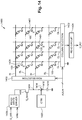
- Figure 14 schematically illustrates a memory array 1400 of resistive-switching elements 100 according to an example embodiment of the present disclosure.
- the array is a crosspoint array, the elements 100 being arranged in rows and columns, and each element 100 being connected between a row line RL of its row, and a column line CL of its column.
- Each element 100 is for example coupled in series with a selector between the row and column lines RL, CL.
- the selector is a transistor 1401 coupled in series with the element 100 via its main current-conducting nodes, and having its gate receiving a selection signal S.
- the selector could be implemented by a diode.
- a row selection circuit (ROW SELECTION) 1402 for example couples a selected row of the array to an input/output node 1404.
- the row selection circuit 1402 also for example generates the selection signal S. For example, all of the elements of each row receive a same signal S, and the rows are controlled independently such that one row of elements 100 can be selected at a time.
- the input/output node 1404 is for example coupled to a read/write driver (READ/WRITE DRIVER) 1406 via a transistor 1408.
- the read/write driver 1406 is for example configured to apply a biasing voltage to a selected element based on a data bit D_WR to be written to the element in a set or reset operation, and/or based on a signal V/NW indicating whether the data bit is to be written in a volatile or non-volatile fashion.
- the read/write driver 1406 is also for example configured to apply a biasing voltage to a selected element during a read operation.
- the read/write driver 1406 is also configured to apply the deep reduction voltage(s) to a selected element via the node 1404.
- the transistor 1408 is for example controlled by a gate voltage Vg, and acts as a current limiter that sets a compliance current during the set operation.
- the input/output node 1404 is also coupled via a switch 1414 to an energy storage node 1416, which is in turn coupled to ground via a capacitor 1418.
- An energy recovery control circuit (CTRL) 1420 for example controls the switch 1414.
- the read/write driver 1406 When energy is to be recovered from a selected element following the dissolution of its filament, the read/write driver 1406 for example applies a deep reduction voltage level to the element.
- the control circuit 1420 then for example activates the switch 1414 to couple the selected element to the energy storage node 1416 and thereby transfer charge to the capacitor 1418.
- the node 1416 is for example coupled to a load, for example via a switch, so that the energy stored to the capacitor 1418 can be extracted following each energy recovery operation.
- a column selection circuit (COLUMN SELECTION) 1422 for example couples a selected element to the ground voltage rail during a write or energy recovery operation, and to a read circuit (READ CIRCUIT) 1424 during a read operation.
- the read circuit 1424 detects a current passing through the selected element in order to read the programmed state of the selected element, and generate an output data bit D_RD.
- the row and column selection circuits 1402, 1422 each for example receives all or part of an address signal ADDR indicating the resistive-switching element to be selected for a given operation.
- control circuit 1420 is provided for the whole array 1400, in alternative embodiments a control circuit could be provided per resistive switching element 100.
- An advantage of the embodiments described herein is that energy can be recovered following the dissolution of a filament of a resistive-switching element.
- the filament is formed during a data programming cycle of the element to store a bit of data by programming the element to have the set state.
- energy is recovered that is a result of a programming operation and that would otherwise have been lost over time. This advantageously permits the energy consumption of the memory to be partially offset, and/or other circuits to be powered.
- each resistive-switching element is programmed to store a single bit by a set operation
- the principles described herein could also be applied to recover energy following the dissolution of a filament storing a plurality of bits of data.
- the element could be set at a selected one of two or more compliance currents, depending on the data bit to be stored, thereby causing different resistance ranges to be programmed.
Landscapes
- Engineering & Computer Science (AREA)
- Chemical & Material Sciences (AREA)
- Materials Engineering (AREA)
- Power Engineering (AREA)
- Semiconductor Memories (AREA)
Abstract
The present disclosure relates to a memory comprising: a resistive-switching element (100) having first and second electrodes (104, 106) separated by a layer of insulator (102); an energy storage component or load coupled to the resistive-switching element (100) via a first switch; and a control circuit (108) configured: to program the resistive-switching element to have a set state, wherein, in the set state, a filament forms a conducting path between the first and second electrodes; and, following a dissolution of the filament, to recover electrical energy, generated by the dissolution of the filament, from one of the first and second electrodes (104, 106) by activating the first switch (S2) .
Description
- The present disclosure relates generally to the field of resistive memories, and more particularly to a method and circuit for recovering energy in resistive-switching memories.
- Resistive random access memory (RRAM) is a well-known class of semiconductor memory technology that is based on the so-called "filamentary switching" effect. Examples of RRAM technologies based on filamentary switching include OxRAM (Oxide Random Access Memory) and CBRAM (conductive bridging RAM). These technologies have advantages in terms of cost, CMOS fabrication process compatibility, and ease of integration.
- Memory elements of a filamentary switching RRAM often have a MIM (metal-insulator-metal) structure, the metal layers forming electrodes, which sandwich the insulator layer there-between. The memory element is initially in an initial resistive state (IRS), which is generally of high resistance. When a voltage above a certain threshold voltage is applied across the metal electrodes, a thin conductive filament is deposited across the insulator creating a conducting path, thereby causing a short circuit to occur between the two metal electrodes, and programming a low resistance state (LRS). A high resistance state (HRS) can then be programmed by applying a voltage of opposite polarity, causing the conductive filament to be dissolved.
- A drawback of the programming operation of RRAM memory elements is thus that it involves non-negligible power consumption.
- It is an aim of embodiments of the present disclosure to at least partially address one or more drawbacks in the prior art.
- For example, it would desirable to increase the overall energy efficiency of an RRAM, and in some cases to recuperate energy that can be used to power or sustain any other generic load external to the memory array. Additionally or alternatively, it would be desirable to provide an RRAM in which recuperated energy contributes to reducing or optimizing the power delivered to the supply rails of the memory array, and/or to any other active block of the integrated circuit chip integrating the memory array.
- According to one embodiment, there is provided a memory comprising: a resistive-switching element having first and second electrodes separated by a layer of insulator; an energy storage component or load coupled to the resistive-switching element via a first switch; and a control circuit configured: to program the resistive-switching element to have a set state, wherein, in the set state, a filament forms a conducting path between the first and second electrodes; and, following a dissolution of the filament, to recover electrical energy, generated by the dissolution of the filament, from one of the first and second electrodes by activating the first switch.
- According to one embodiment, the energy storage component or load comprises: a capacitor; or an inductor; or a resistor; or any combination of two or three of the above.
- According to one embodiment, the control circuit is configured to apply a biasing voltage of a first level and having a first polarity across the first and second electrodes in order to program the set state.
- According to one embodiment, the control circuit is further configured to apply a biasing voltage of a second level, and having a second polarity opposite to the first polarity, across the first and second electrodes in order to dissolve the filament.
- According to one embodiment, the control circuit is further configured to apply a biasing voltage of a third level, and having the second polarity, across the first and second electrodes prior to recovering the electrical energy, the third level having a greater absolute value than the second level.
- According to one embodiment, the third level is in the range -0.5 to -5 V, and for example in the range -1 to -3 V.
- According to one embodiment, the third level has an absolute value that is equal to or greater than a fourth level at which a current conducted by the resistive-switching element falls to zero.
- According to one embodiment, the control circuit is further configured to apply a biasing voltage of a fifth level, and having the second polarity, across the first and second electrodes prior to recovering further energy, the fifth level having a greater absolute value than the third level.
- According to one embodiment, the memory comprises a second switch coupling the first electrode of the resistive-switching element to a biasing circuit, the first switch couples the first electrode of the resistive-switching element to an energy storage node, and the control circuit is configured to recover electrical energy from one of the first and second electrodes by deactivating the second switch and activating the first switch.
- According to one embodiment, the memory further comprises a third switch coupling the energy storage node to the load.
- According to one embodiment, the memory comprises an array formed of the resistive-switching element and a plurality of further resistive-switching elements having first and second electrodes.
- According to one embodiment, the control circuit is further configured to recover electrical energy from one of the first and second electrodes of each of the further resistive-switching elements following a dissolution of the filament of each resistive-switching element.
- According to one embodiment, the memory further comprises a plurality of further control circuits for controlling the plurality of further resistive-switching elements.
- According to a further aspect, there is provided a method of programming a resistive-switching element having first and second electrodes, the method comprising: programming, by a control circuit, the resistive-switching element to have a set state wherein, in the set state, a filament forms a conducting path between the first and second electrodes; and following a dissolution of the filament, recovering, from one of the first and second electrodes, electrical energy generated by the dissolution of the filament by activating a first switch, the first switch coupling the resistive-switching element to a load.
- According to one embodiment, programming the resistive-switching element to have the set state comprises applying, by the control circuit, a biasing voltage of a first level and having a first polarity across the first and second electrodes.
- According to one embodiment, the method further comprises applying, by the control circuit, a biasing voltage of a second level, and having a second polarity opposite to the first polarity, across the first and second electrodes in order to dissolve the filament.
- According to one embodiment, the method further comprises applying, by the control circuit, a biasing voltage of a third level, and having the second polarity, across the first and second electrodes prior to recovering the electrical energy, the third level having a greater absolute value than the second level.
- According to one embodiment, the third level is in the range -0.5 to -5 V, and for example in the range -1 to -3 V.
- The foregoing features and advantages, as well as others, will be described in detail in the following description of specific embodiments given by way of illustration and not limitation with reference to the accompanying drawings, in which:
-
Figure 1 schematically illustrates a resistive-switching element according to an example embodiment; -
Figure 2 illustrates an example of forming, set and reset programming phases of the resistive-switching element ofFigure 1 according to an example embodiment; -
Figure 3 schematically represents non-volatile and volatile programming cycles of a resistive-switching element according to an example embodiment; -
Figure 4 is a graph representing an example of operating voltage and current ranges for a memory mode and an energy recuperation mode of a resistive-switching element according to an example embodiment of the present disclosure; -
Figure 5 is a graph representing current and voltage during a programming and energy recovery cycle of a resistive-switching element according to an example embodiment of the present disclosure; -
Figure 6 is a flow diagram schematically illustrating operations in a method of non-volatile programming and energy recovery in a resistive-switching element according to an example embodiment of the present disclosure; -
Figure 7 is a flow diagram schematically illustrating operations in a method of volatile programming and energy recovery in a resistive-switching element according to an example embodiment of the present disclosure; -
Figure 8 is a timing diagram representing an example of voltage levels during non-volatile and volatile programing cycles of a resistive-switching element according to an example embodiment of the present disclosure; -
Figure 9 is a timing diagram representing an example of voltage levels during non-volatile and volatile programing cycles of a resistive-switching element according to a further example embodiment of the present disclosure; -
Figure 10 schematically illustrates set and reset operations during non-volatile programming of a memory circuit comprising a resistive-switching element according to an example embodiment of the present disclosure; -
Figure 11 schematically illustrates capacitor charging and discharging operations of the memory circuit ofFigure 10 according to an example embodiment of the present disclosure; -
Figure 12 schematically illustrates a set operation during volatile programming of the memory circuit ofFigure 10 according to an example embodiment of the present disclosure; -
Figure 13 is a timing diagram representing an example of voltage levels during a reset and deep reduction operation of a resistive-switching element according to an example embodiment of the present disclosure; and -
Figure 14 schematically illustrates a memory array of resistive-switching elements according to an example embodiment of the present disclosure. - Like features have been designated by like references in the various figures. In particular, the structural and/or functional features that are common among the various embodiments may have the same references and may dispose identical structural, dimensional and material properties.
- Unless indicated otherwise, when reference is made to two elements connected together, this signifies a direct connection without any intermediate elements other than conductors, and when reference is made to two elements linked or coupled together, this signifies that these two elements can be connected or they can be linked or coupled via one or more other elements.
- In the following disclosure, unless indicated otherwise, when reference is made to absolute positional qualifiers, such as the terms "front", "back", "top", "bottom", "left", "right", etc., or to relative positional qualifiers, such as the terms "above", "below", "higher", "lower", etc., or to qualifiers of orientation, such as "horizontal", "vertical", etc., reference is made to the orientation shown in the figures.
- Unless specified otherwise, the expressions "around", "approximately", "substantially" and "in the order of" signify within 10 %, and preferably within 5 %.
-
Figure 1 schematically illustrates an example of a resistive-switchingelement 100 that operates based on filamentary switching. Theelement 100 has a MIM structure comprising a layer of insulator (INSULATOR) 102 forming an electrolyte and sandwiched between a top metal electrode (METAL) 104 at a voltage VTE and a bottom metal electrode (METAL) 106 at a voltage VBE. Theelement 100 is capable of storing a bit of data under control of a biasing voltage VBIAS applied across itselectrodes -
Figure 1 also illustrates a control circuit (CTRL) 108 configured, for example, to generate the biasing voltage VBIAS for applying across the electrodes of theelement 100, for example based on input data D_WR to be written to the element. Thecontrol circuit 108 is also for example configured to recover electrical energy from one of theelectrodes element 100, as will be described in more detail below. - Operation of the
element 100 for data storage will now be described with reference toFigure 2 . -
Figure 2 illustrates an example of forming, set and reset programming phases of the resistive-switchingelement 100 ofFigure 1 . - Prior to any programming operation, the
element 100 is for example in an initial resistive state (IRS). A process known as forming or electroforming (FORMING) involves applying a biasing voltage VBIAS across the electrodes of theelement 100 to cause a transition from the IRS state to a low resistance state (LRS). - Thereafter, the
element 100 can for example be made to toggle between the low resistance state and a high resistance state (HRS), these states being respectively associated with distinguishable low and high resistance values in order to provide binary data storage. In particular, a transition from the LRS state to the HRS state is generally referred to as a reset operation (RESET), and the HRS state is generally considered to correspond to a logic "0" state or OFF state. A transition from the HRS state to the LRS state is generally referred to as a set operation (SET), and the LRS state is generally considered to correspond to a logic "1" state or ON state. - Transitioning from the IRS or HRS state to the LRS state involves applying a biasing voltage VBIAS across the resistive-switching
element 100 in order to form afilament 202 across the insulatinglayer 102. This filament forms a conducting path between theelectrodes - Transitioning from the LRS state to the HRS state involves at least partially dissolving the
filament 202 such that there is no longer a short circuit between theelectrodes - The particular mechanism that causes the creation and dissolution of the filament across the insulating
layer 102 depends on the particular technology of the resistive-switching element, and will not be described in detail herein. For example, conductive bridge RAM is described in more detail in the publication by D.Jana et al. entitled "Conductive-bridging random access memory: challenges and opportunity for 3D architecture", Nanoscale Research Letters, 2015. Oxide Random Access Memory is for example described in more detail in the publication by H.S.Philip Wong et al. entitled "Metal-Oxide RRAM", Proceedings of the IEEE, 2012. The contents of these two publications is for example incorporated herein by reference to the extent permitted by the law. -
Figure 3 schematically represents non-volatile and volatile programming cycles of a resistive-switching element such as theelement 100 ofFigure 1 . - A sequence A in
Figure 3 represents a non-volatile programming cycle, which for example involves a non-volatile set operation (NON-VOLATILE SET) creating afilament 302 between the electrodes of the element. The operation is considered non-volatile because enough power is applied to the element during the set process that the resulting filament is relatively thick, and therefore is not dissolved in the absence of an external bias. For example, the non-volatile LRS state is maintained for a relatively long duration, such as months or years. - Sometime later, the LRS state is for example read during a read operation (READ), involving detecting the low resistance state of the element and outputting the associated logic level, which is for example a logic "1".
- When the element is next to be programmed at the high resistance state, a reset operation (RESET) is applied by biasing the element with a biasing voltage VBIAS of opposite polarity to the one used during the set operation. The result is for example that only a
portion 304 of thefilament 302 remains, and thus there is a relatively high resistance between the electrodes of the element. This reset state is always non-volatile in that the filament will not be reformed in the absence of an appropriate biasing voltage VBIAS applied across the electrodes. - Like for the LRS state, sometime later, the HRS state is for example read during a further read operation (READ), involving detecting the high resistance state of the element and outputting the associated logic level, which is for example a logic "0".
- A sequence B in
Figure 3 represents a volatile programming cycle, which for example involves a volatile set operation (VOLATILE SET) creating afilament 306 between the electrodes of the element. The operation is considered volatile because relatively low power is applied to the element during the set process and so the resultingfilament 306 is relatively thin, and will tend to self-dissolve after a limited time window, which will be referred to herein as a retention time window. For example, the volatile LRS state is maintained for a relatively short duration of between 1 µs and several days, and in some embodiments of two days at most. - A short time later, and before the LRS state self-dissolves, the LRS state is for example read during a read operation (READ), involving detecting the low resistance state of the element and outputting the associated logic level, which is for example a logic "1". In some embodiments, a DRAM (dynamic RAM) operation is applied according to which elements programmed to have the LRS state are refreshed by a new volatile set if they are to store their data beyond the end of the retention time window. In such a case, the read operation is for example part of a refresh operation of the element, and after reading the LRS state, this state is reprogrammed in order to extend the data storage duration.
- A self reset event (SELF RESET) for example occurs at the end of the retention time window. The result of this self reset event is for example that only a
portion 308 of thefilament 306 remains, and thus there is a relatively high resistance between the electrodes of the element. - Sometime later, this time lapse not being limited by any time window, the HRS state is for example read during a further read operation (READ), involving detecting the high resistance state of the element and outputting the associated logic level, which is for example a logic "0". As represented by
dots 310 inFigure 3 , by the time of the read operation the conductive particles of the filament may have entirely dissolved and dispersed in the insulator. - It has been shown that an electromotive force is generated by programing operations of a resistive-switching element, this force appearing in the form of a non-zero voltage, which will be called Vemf, across the electrodes of the element. For example, the existence of such a force was described in the French patent applications published as
FR3061599 FR3066043 - For example, the following table provides approximate measured voltages VCELL for CBRAM and OxRAM elements having different materials for the top electrode (TE), the insulator (INSUL) and the bottom electrode (BE). The voltage VCELL is a voltage measured across the cells electrodes in open circuit conditions after "charging".
[Table 1] Technology Materials of TE/INSUL/BE VCELL (mV) CBRAM Cu/SiO2/Pt 300 Ag/SiO2/Pt 150 Ag/GeSx/Pt 120 Ag/GeSex/ Pt 100 Cu/WO3/Pt 40 Ag/Agl/ Pt 2 OxRAM Pt/SrTiO3/Ti (as deposited) 200 Pt/SrTiO3/Ti 1.5 Pt/Ta2O5/Ta 0.05 - The present inventors propose a method and circuit for harvesting the energy resulting from this electromotive force, as will now be described with reference to
Figures 4 to 14 . -
Figure 4 is a graph representing an example of operating voltage VBIAS and current ranges for a memory mode and an energy recuperation mode of a resistive-switching element according to an example embodiment of the present disclosure. - The memory mode corresponds to the use of the programming cycles of the resistive-switching element for data storage, as described above in relation with
Figure 3 . The memory mode for example involves applying biasing voltages VBIAS across the electrodes of the resistive-switching element in the range of around -3 to 3 V, with currents anywhere in the range of 1 fA to 1 mA, and preferably of 1 µA to 100 µA. - The energy recuperation mode corresponds to the presence, while not in the set state, of a voltage across the electrodes of the resistive-switching element, which can be harvested. In the example of
Figure 4 , the energy recuperation mode is compatible with voltages in the range from -8 V up to the voltage at which the filament is formed, which is for example at around 1 V. The present inventors have found that, as long as the filament is not formed, the energy recuperation mode is, however, more generally compatible with biasing voltages VBIAS in the range from around -10 to 10 V, and for example in the range from -5 to 5 V, and with currents anywhere in the range of 1 fA to 1 mA, and preferably of 1 µA to 100 µA. - There is thus an overlapping biasing voltage range between the memory mode and the energy recuperation mode from around -3 V to around 1 V. The present inventors propose to exploit this range in order to harvest energy during memory programming cycles. In some cases, the biasing voltage VBIAS may be brought below -3 V during the energy recovery. For example, the voltage is varied in the range between -5 and 1 V.
-
Figure 5 is a graph representing a current and biasing voltage VBIAS during a programming and energy recovery cycle of a resistive-switching element according to an example embodiment of the present disclosure. This graph was obtained by a technique of quasi-static memory characterization involving biasing the resistive-switching element with a ramping voltage source corresponding to the voltage VBIAS across the two electrodes of the element, while measuring the current across the electrodes. The biasing voltage VBIAS is swept from a negative voltage of relatively high absolute value to a positive voltage of relatively high absolute value, and back again, in order to characterize the behavior of the element during a programming cycle. - In the example of
Figure 5 , the biasing voltage VBIAS starts at a point (1) at around -2 V. The resistive-switching element is for example in the IRS or HRS state. In this state, the resistive-switching element undergoes no change by the external bias, as substantially no ion is being produced, and no electromotive force can thus arise. - The biasing voltage VBIAS across the electrodes of the element is then increased, for example by a voltage ramp. At a certain positive voltage level, equal for example to between 0.1 and 0.5 V, the interface between the top electrode and electrolyte layer starts to undergo oxidation, and metal cations are released inside the electrolyte. For example, this occurs in accordance with the general expression:

- An electromotive force starts to arise mainly due to the ionic gradient present inside the electrolyte layer. As the voltage increases further, the oxidation is enhanced and more metal ions are produced and consequently either diffuse or are swept by the electric field to the bottom electrode, where they are reduced, and lose their charged state.
- Eventually, enough atoms pile up and bridge the two electrodes of the resistive-switching element, thus allowing the current to jump to a compliance value, which is for example set in the
range 1 to 100 µA, and for example at around 50 µA in the example ofFigure 5 , corresponding in this case to a non-volatile set operation. This is represented by a risingedge 502 of the current-voltage curve, which for example occurs at a voltage V_SET, equal to around 0.5 V in the example ofFigure 5 . The element has thus reached its SET state at (3), and any electromotive force across the electrodes is lost due to the presence of the short circuit. Therefore, in some embodiments, the biasing voltage VBIAS is not increased much higher than the voltage V_SET, and for example not more than around V_SET+0.5 V, equal to around 1 V in the exampleFigure 5 . - When the biasing voltage VBIAS is then swept in the opposite direction, the filament is stable until enough energy is provided to dissolve it. As the biasing voltage VBIAS approaches 0 V, the current starts to fall rapidly, and turns negative when the voltage becomes negative. At (4), the biasing voltage VBIAS reaches a level of V_RESET, equal to around -0.15 V in the example of
Figure 5 , and dissolution occurs, which corresponds to the reset taking place. For some types of resistive-switching memory, this is for example a mainly thermic reset process, which occurs due to Joule heating. Thereafter, as the biasing voltage VBIAS becomes more negative, a reduction in metal cations coming from the dissolving filament becomes the dominant contribution. The general reduction can be written as:
- The current has a
trough 504 when the biasing voltage VBIAS reaches a level V_Imin, equal to around -0.4 V in the example ofFigure 5 . - The voltage range from V_Imin to a little over V_SET, for example V_SET plus between 1 and 10 percent, represented by a dashed
rectangle 506 inFigure 5 , corresponds for example to the memory programming voltage range. However, the present inventors have found that, following the dissolution of the filament, a more negative voltage range from V_Imin to a discharged level V_DISCHG at (5), and represented by ashaded rectangle 508 inFigure 5 , is associated with a furthercurrent peak 510, corresponding to a peak electromotive force. This peak corresponds to a reduction peak, and thevoltage range 508 from V_Imin to V_DISCHG corresponds to a deep reduction regime. Indeed, at (5), when the biasing voltage VBIAS is equal to or lower than V_DISCHG, a major number of metal cations have been either reduced back to the top electrode of the resistive-switching element and have lost their charge, or they have been attracted to the TE/electrolyte interface. As a result, at (5), an electromotive force is obtained by stopping the voltage in the shadedarea 508, in other words by reducing the voltage to a final level within the range V_Imin to V_DISCHG, and then placing the resistive-switching element in open circuit. The final voltage level is for example determined during a calibration step in order to achieve a relatively high, or maximum, electromotive force Vemf. In the example ofFigure 5 , the voltage V_DISCHG is equal to around -1.3 V. The present inventors have found that the closer the reset voltage gets to the level V_DISCHG corresponding to the negative limit of the deep reduction regime, the greater the energy that can be recovered. Indeed, the maximum charge that can be generated is met when this point is reached, as below this point, the reaction resulting in the charge generation ceases to occur. However, applying a more negative voltage is likely to also consume more energy than applying a less negative voltage, and therefore the calibration step can be used to find an optimum or close to optimum voltage level to be applied for energy recuperation. - Methods of exploiting the effects indicated above in relation with
Figure 5 in order to recover energy during non-volatile and volatile programming cycles of a resistive-switching element will now be described with reference toFigures 6 ,7, 8 and 9 . -
Figure 6 is a flow diagram schematically illustrating operations in amethod 600 of non-volatile programming and energy recovery in a resistive-switching element according to an example embodiment of the present disclosure. This method is for example implemented by thecontrol circuit 108 ofFigure 1 . -
Figure 7 is a flow diagram schematically illustrating operations in amethod 700 of volatile programming and energy recovery in a resistive-switching element according to an example embodiment of the present disclosure. This method is also for example implemented by thecontrol circuit 108 ofFigure 1 , and may for example be performed in addition to the method ofFigure 6 . For example, thecontrol circuit 108 is capable of both volatile and non-volatile programming of a same resistive-switching element. - While in the methods of
Figures 6 and7 one or more read operations are for example performed to read the programmed state of the resistive-switching element, in the case that the memory mode is not required, these read operations could be omitted, resulting in an energy storage and recuperation mode, similar to a battery function. -
Figures 8 and 9 are timing diagrams representing examples of levels of the biasing voltage VBIAS during non-volatile and volatile programing cycles of a resistive-switching element. - With reference first to
Figure 6 , the non-volatile programming and energy recovery cycle for example starts with anoperation 601, in which a non-volatile set (NON-VOLATILE SET) is performed. - For example, as represented by a solid curve in
Figure 8 , the non-volatile set is performed by applying a voltage ramp to bring the biasing voltage VBIAS from 0 V to a SET voltage VSET, where this SET voltage is for example equal to or higher to the level V_SET ofFigure 5 . In some embodiments, the voltage VSET is in the range 0.5 to 2 V. At the end of the SET operation, the resistive-switching element is for example placed in open circuit, to interrupt any biasing voltage VBIAS across the element. - Alternatively, as represented by a solid curve in
Figure 9 , the non-volatile set is performed by applying a uniform voltage pulse at the SET voltage VSET. Again, the voltage VSET is for example equal to or higher to the level V_SET ofFigure 5 . In some embodiments, the voltage VSET in the example ofFigure 9 is in the range 0.3 to 1.5 V. Like for the voltage ramp ofFigure 8 , at the end of the uniform voltage pulse ofFigure 9 , the resistive-switching element is for example placed in open circuit, to interrupt any biasing voltage VBIAS across the cell. - Whatever the form of the voltage, during the non-volatile SET operation, the current through the resistive-switching element is for example limited to a compliance current, which is for example of at least 20 µA, and for example in the range 20 µA to 200 µA, and in some cases in the range 50 µA to 100 µA. For example, the resistive-switching element is coupled or connected in series with a transistor, as shown for example in
Figure 14 below. This transistor is for example gate-biased by a voltage level controlled such that the maximum current is limited to the compliance current. - With reference again to
Figure 6 , in anoperation 602, a read operation (READ) is then for example performed, to read the SET state programmed inoperation 601. This operation for example involves measuring a current passing through the resistive-switching element while a read voltage is applied to the element, or measuring a voltage across the resistive-switching element while a read current is passed through the element. Such a read operation is well known in the art and will not be described in more detail. - In an
operation 603, reset and deep reduction (RESET AND DEEP REDUCTION) is performed. - For example, as represented by the solid curve in
Figure 8 , this involves applying a negative biasing voltage VBIAS in the form of a ramp starting, for example, at 0 V and falling to a negative deep reduction voltage VDR. The ramp for example has a duration of over 1 ms, and for example of 5 ms or more. Alternatively, rather than a ramp, a constant voltage could be applied for a similar time duration to the ramp, at the negative deep reduction voltage VDR. The voltage VDR is for example lower than the voltage VRESET causing the reset process to occur, and is also lower than the voltage V_Imin ofFigure 5 , at which the current falls to the low 504. In some embodiments, the voltage VDR is in the range -0.5 to -5 V, and for example in the range -1 to -2 V. At the end of the negative ramp or constant voltage, the resistive-switching element is for example placed in open circuit, the biasing voltage being represented inFigure 8 by a dotted line during the open circuit period. Indeed, if the biasing voltage VBIAS were to be reduced to 0 V while being applied to the resistive-switching element, this would effectively short-circuit the electrodes of the element across which it is desired to recuperate energy, forcing the electromotive force Vemf of the cell to 0 V. - Alternatively, as represented by the solid curve in
Figure 9 , the reset and deep reduction operation involves applying a negative pulse corresponding to a biasing voltage VBIAS at the level of VRESET, and then, for example after placing the resistive-switching element in open circuit, applying a ramp starting at VRESET, and then falling to the negative deep reduction voltage VDR. Again the voltage VDR inFigure 9 is for example lower than the voltage VRESET causing the reset process to occur, and is also lower than the voltage V_Imin ofFigure 5 , at which the current falls to the low 504. In some embodiments, the voltage VDR is in the range -1 to -5 V, and for example in the range -1 to -2 V. At the end of the negative ramp, the resistive-switching element is for example placed in open circuit, as represented by a dotted line inFigure 9 . - With reference again to
Figure 6 , in anoperation 604, energy recovery (ENERGY RECOVERY) is for example performed. In particular, energy that was generated by the dissolution of the filament is at least partially recovered. This for example involves transferring charge present at the top electrode of the resistive-switching element to a capacitor or other storage means or load. This energy recovery operation is for example performed relatively soon after the reset operation, as it has been found that the voltage present across the element due to electromotive force tends to disappear after a certain duration ranging from a few seconds to several hundred seconds, depending on the technology of the element. For example, the energy recovery operation is performed within 5 seconds of the reset operation, and in some cases within 1 second or even within 100 ms of the reset operation. - After the
energy recovery operation 604, a further read operation (READ) 605 is for example performed in order to read the reset state of the element, this operation being performed in a similar manner to the readoperation 602. Advantageously, this further read operation of the reset state is performed after the energy recovery operation, thereby recovering energy that would otherwise be lost during the read operation. - With reference now to
Figure 7 , the volatile programming and energy harvesting cycle for example starts with an operation 701, in which a volatile set (VOLATILE SET) is performed. This operation for example involves applying the same voltages as in the example ofFigure 8 or 9 discussed above. However, whatever the form of the voltage, during the volatile SET operation, the current through the resistive-switching element is for example limited to a compliance current lower than the one used for a non-volatile set operation. For example, the compliance current is limited to a level of less than 20 µA, and for example to a level in therange 100 fA to 20 µA, and in some cases to a level in therange 1 nA to 10 µA. - In an
operation 702, a read operation (READ) is then for example performed, to read the SET state programmed in operation 701. This operation for example involves measuring a current passing through the resistive-switching element while a read voltage is applied to the element, or measuring a voltage across the resistive-switching element while a read current is passed through the element. Such a read operation is well known in the art and will not be described in more detail. The read operation is for example performed within the retention time window of the volatile SET state, which for example depends on the compliance current and duration of the SET operation. Indeed, after the retention time window, the filament will dissolve spontaneously, after which the SET state can no longer be read. - In an
operation 703, self reset occurs. As indicated above, this for example occurs at the end of the retention time window of the resistive-switching element. Thus, whereas in the examples ofFigures 8 and 9 negative biasing voltages are applied in order to perform a reset operation following a programmed non-volatile set state, for a programmed volatile set state, the resistive-switching element is for example kept in open circuit and self reset occurs naturally. - In an
operation 704, energy recovery (ENERGY RECOVERY) is for example performed. In particular, energy that was generated by the dissolution of the filament is at least partially recovered. Like in the case of non-volatile programming, this for example involves transferring charge present at the electrodes of the resistive-switching element to a capacitor or other storage means or load, as will be described in more detail below with reference toFigure 10 . However, in this case, there is for example no reset voltage VRESET or deep reduction voltage VDR applied to the element. - Alternatively, it would also be possible to apply a reset voltage VRESET and/or deep reduction voltage VDR in the
energy recovery operation 704, for example in order to increase the amount of recuperated energy. This energy recovery operation is for example performed relatively soon after the reset operation, as it has been found that the voltage present across the element due to electromotive force tends to disappear after a certain duration ranging from a few seconds to several hundred seconds, depending on the technology of the element. For example, the energy recovery operation is performed within 5 seconds of the reset operation, and in some cases within 1 second or even within 100 ms of the reset operation. In some embodiments, the energy recovery using the reset voltage VRESET and/or deep reduction voltage VDR is performed during each refresh cycle of the resistive-switching element described above. For example, the set state read in the readoperation 702 is written back during the refresh operation following the energy recovery. - In some embodiments, after the
energy recovery operation 704, a further read operation (READ) 705 is performed in order to read the reset state of the element, this operation being performed in a similar manner to the readoperation 702. -
Figure 10 schematically illustrates set and reset operations during non-volatile programming of amemory circuit 1000 comprising the resistive-switchingelement 100. Thememory circuit 1000 for example comprises the series connection of a switch S1 and the resistive-switchingelement 100 between input/output lines control circuit 108, the biasing voltage VBIAS being provided across theselines intermediate node 1008 between the switch S1 and theelement 100 is for example coupled to anenergy storage node 1010 via a switch S2. A capacitor C for example provides this energy storage, and is coupled between theenergy storage node 1010 and the input/output line 1006. A switch S3 is for example coupled between thenode 1010 and a load ZL. The load ZL is for example a resistive and/or inductive load. - The switches S1, S2 and S3 are for example controlled by the
control circuit 108. - In alternative embodiments, the switches S2 and S3, capacitor C and load ZL could be replaced by any charge storage component or inductive and/or resistive load coupled to the
element 100 via one or more switches. -
Figure 10 shows, on the left, the non-volatile set operation (NON-VOLATILE SET) during which the switch S1 is conducting, and the switches S2 and S3 are in open-circuit. Furthermore, thecontrol circuit 108 provides the biasing voltage VBIAS for setting theelement 100, for example using a positive voltage ramp or other waveform. -
Figure 10 also shows, on the right, the reset operation (RESET) during which the switches S1, S2 and S3 are controlled in the same manner as for the SET operation, and thecontrol circuit 108 provides the biasing voltage VBIAS for resetting theelement 100, for example using a negative voltage ramp or other waveform. -
Figure 11 schematically illustrates capacitor charging and discharging operations of thememory circuit 1000 ofFigure 9 during energy recovery. -
Figure 11 shows, on the left, the charging operation (CHARGING C) during which the switches S1 and S3 are for example in open circuit, and the switch S2 is conducting. Thus, thenode 1008 is coupled to the capacitor C, and the charge present across theelement 100 is for example transferred to the capacitor C. For example, as described in more detail below, in a memory array of resistive-switching elements, the recuperated energy from each element is used to power or sustain any generic load external to the memory array. Additionally or alternatively, the recuperated energy for example contributes to reducing or optimizing the power delivered to the supply rails of the memory array, and/or to any other active block of the integrated circuit chip integrating the memory array. -
Figure 11 also shows, on the right, the discharging operation (DISCHARGE TO LOAD) during which the switches S1 and S2 are for example in open circuit, and the switch S3 is conducting. Thus, the charge stored on the capacitor C is transferred to the load. For example, in one embodiment the load could be a circuit for charging a battery, or any other type of load. -
Figure 12 schematically illustrates a set operation during volatile programming of thememory circuit 1000 ofFigures 10 and 11 . -
Figure 12 shows the volatile set operation (VOLATILE SET) during which the switch S1 is conducting, and the switches S2 and S3 are in open-circuit. Furthermore, thecontrol circuit 108 provides the biasing voltage VBIAS for setting theelement 100, for example using a positive voltage ramp or other waveform. However, as explained above, thecontrol circuit 108 is for example configured to limit the current through theelement 100 to a relatively low compliance current, leading to a volatile set operation. - The volatile set operation of
Figure 12 is for example followed by capacitor charging and discharging operations, which are for example the same as those ofFigure 11 , and will not be described again in detail. - While in the embodiments described above energy is recovered from the resistive-switching element in a single transfer, in alternative embodiments, the energy could be recovered progressively, as will now be described in more detail with reference to
Figure 13 . -
Figure 13 is a timing diagram representing an example of levels of the biasing voltage VBIAS during a reset and deep reduction operation of a resistive-switching element according to an example embodiment of the present disclosure. - The biasing voltage VBIAS is for example progressively reduced by applying a series of negative voltage ramps having increasing absolute levels. Each of the ramps is for example a quasi-static ramp in that the voltage variation is relatively slow with respect to the ramp duration, which is for example of 1 ms or more. In the example of
Figure 13 , afirst ramp 1301 has an absolute amplitude that increases over time, for example in a linear manner, from the level VRESET to a level VDR1, which is more negative than VRESET. Similarly, asecond ramp 1302 increases from the level VDR1 to a level VDR2, which is more negative than VDR1, athird ramp 1303 increases from the level VDR2 to a level VDR3, which is more negative than VDR2, and afourth ramp 1304 increases from the level VDR3 to a level VDR4, which is more negative than VDR3. In between each ramp and at the end of the final ramp, the resistive-switching element is for example placed in open circuit, as represented by a dotted line inFigure 13 . - Energy is for example recovered from the resistive-switching element following each of the ramps VDR1 to VDR4. The timing between the ramps may vary, and be selected as a function of the energy needs of the circuit.
- In alternative embodiments, there could be only two or three ramps, or more than four ramps, in the series. The resistive-switching element is for example placed in open-circuit between each ramp. The level of each ramp VDR1 to VDRn, where n is the final ramp, is for example in the range -0.5 to -5 V, and for example in the range -0.5 V to -2 V. The levels and durations of each ramp and the number of ramps are for example chosen such that only the final ramp VDRn causes the current through the element to fall to zero, corresponding to the point at V_DISCHG of
Figure 5 . In some embodiments, rather than using a fixed number of ramps, the ramps are stopped based on the detection of a peak current corresponding to thepeak 510 ofFigure 5 . For example, if p ramps have been applied to bring the current to thepeak 510, the ramps are stopped after a further p ramps have been applied. Alternatively, in some cases the detection of the current peak may be rendered difficult due to leakage or tunneling currents. Therefore, rather than detecting the current peak, the voltage value of VBIAS at which to stop could be found, during a calibration step, by cycling over increasingly negative voltages until a level is found below which the voltage Vemf across the cell reaches a maximum and does not increase anymore. -
Figure 14 schematically illustrates amemory array 1400 of resistive-switchingelements 100 according to an example embodiment of the present disclosure. - In the example of
Figure 14 , the array is a crosspoint array, theelements 100 being arranged in rows and columns, and eachelement 100 being connected between a row line RL of its row, and a column line CL of its column. Eachelement 100 is for example coupled in series with a selector between the row and column lines RL, CL. In the example ofFigure 14 , the selector is atransistor 1401 coupled in series with theelement 100 via its main current-conducting nodes, and having its gate receiving a selection signal S. In alternative embodiments, the selector could be implemented by a diode. - A row selection circuit (ROW SELECTION) 1402 for example couples a selected row of the array to an input/
output node 1404. Therow selection circuit 1402 also for example generates the selection signal S. For example, all of the elements of each row receive a same signal S, and the rows are controlled independently such that one row ofelements 100 can be selected at a time. - The input/
output node 1404 is for example coupled to a read/write driver (READ/WRITE DRIVER) 1406 via atransistor 1408. The read/write driver 1406 is for example configured to apply a biasing voltage to a selected element based on a data bit D_WR to be written to the element in a set or reset operation, and/or based on a signal V/NW indicating whether the data bit is to be written in a volatile or non-volatile fashion. The read/write driver 1406 is also for example configured to apply a biasing voltage to a selected element during a read operation. - In some embodiments, the read/
write driver 1406 is also configured to apply the deep reduction voltage(s) to a selected element via thenode 1404. - The
transistor 1408 is for example controlled by a gate voltage Vg, and acts as a current limiter that sets a compliance current during the set operation. - The input/
output node 1404 is also coupled via aswitch 1414 to anenergy storage node 1416, which is in turn coupled to ground via acapacitor 1418. An energy recovery control circuit (CTRL) 1420 for example controls theswitch 1414. - When energy is to be recovered from a selected element following the dissolution of its filament, the read/
write driver 1406 for example applies a deep reduction voltage level to the element. Thecontrol circuit 1420 then for example activates theswitch 1414 to couple the selected element to theenergy storage node 1416 and thereby transfer charge to thecapacitor 1418. While not illustrated inFigure 14 , thenode 1416 is for example coupled to a load, for example via a switch, so that the energy stored to thecapacitor 1418 can be extracted following each energy recovery operation. - A column selection circuit (COLUMN SELECTION) 1422 for example couples a selected element to the ground voltage rail during a write or energy recovery operation, and to a read circuit (READ CIRCUIT) 1424 during a read operation. For example, during a read operation, the
read circuit 1424 detects a current passing through the selected element in order to read the programmed state of the selected element, and generate an output data bit D_RD. - The row and
column selection circuits - While in the example of
Figure 14 asingle control circuit 1420 is provided for thewhole array 1400, in alternative embodiments a control circuit could be provided perresistive switching element 100. - An advantage of the embodiments described herein is that energy can be recovered following the dissolution of a filament of a resistive-switching element. In some embodiments, the filament is formed during a data programming cycle of the element to store a bit of data by programming the element to have the set state. In other words, energy is recovered that is a result of a programming operation and that would otherwise have been lost over time. This advantageously permits the energy consumption of the memory to be partially offset, and/or other circuits to be powered.
- Various embodiments and variants have been described. Those skilled in the art will understand that certain features of these embodiments can be combined and other variants will readily occur to those skilled in the art. For example, while embodiments have been described in which each resistive-switching element is programmed to store a single bit by a set operation, the principles described herein could also be applied to recover energy following the dissolution of a filament storing a plurality of bits of data. For example, the element could be set at a selected one of two or more compliance currents, depending on the data bit to be stored, thereby causing different resistance ranges to be programmed.
Claims (15)
- A memory comprising:- a resistive-switching element (100) having first and second electrodes (104, 106) separated by a layer of insulator (102);- an energy storage component (C) or load (ZL) coupled to the resistive-switching element (100) via a first switch (S2, 1414); and- a control circuit (108) configured: to program the resistive-switching element to have a set state, wherein, in the set state, a filament (202, 302, 306) forms a conducting path between the first and second electrodes; and, following a dissolution of the filament, to recover electrical energy, generated by the dissolution of the filament, from one of the first and second electrodes (104, 106) by activating the first switch (S2).
- The memory of claim 1, wherein the energy storage component (C) or load (ZL) comprises:- a capacitor; or- an inductor; or- a resistor; or- any combination of two or three of the above.
- The memory of claim 1 or 2, wherein the control circuit (108) is configured to apply a biasing voltage (VBIAS) of a first level (VSET) and having a first polarity across the first and second electrodes (104, 106) in order to program the set state.
- The memory of claim 3, wherein the control circuit (108) is further configured to apply a biasing voltage (VBIAS) of a second level (VRESET, VDR), and having a second polarity opposite to the first polarity, across the first and second electrodes (104, 106) in order to dissolve the filament.
- The memory of claim 4, wherein the control circuit (108) is further configured to apply a biasing voltage (VBIAS) of a third level (VDR, VDR1), and having the second polarity, across the first and second electrodes (104, 106) prior to recovering the electrical energy, the third level (VDR) having a greater absolute value than the second level (VRESET).
- The memory of claim 5, wherein the third level (VDR) is in the range -0.5 to -5 V, and for example in the range -1 to -3 V.
- The memory of claim 5 or 6, wherein the third level (VDR) has an absolute value that is equal to or greater than a fourth level (V_DISCHG) at which a current conducted by the resistive-switching element (100) falls to zero.
- The memory of claims 5 or 6, wherein the control circuit (108) is further configured to apply a biasing voltage (VBIAS) of a fifth level (VDR2), and having the second polarity, across the first and second electrodes (104, 106) prior to recovering further energy, the fifth level (VDR2) having a greater absolute value than the third level (VDR, VDR1) .
- The memory of any of claims 1 to 8, comprising a second switch (S1, 1408) coupling the first electrode (104) of the resistive-switching element (100) to a biasing circuit (108, 1406, 1408, 1410), wherein the first switch (S2, 1414) couples the first electrode (104) of the resistive-switching element (100) to an energy storage node (1008, 1416), and wherein the control circuit (108) is configured to recover electrical energy from one of the first and second electrodes (104, 106) by deactivating the second switch (S1, 1408) and activating the first switch (S2, 1414).
- The memory of claim 9, further comprising a third switch (S3) coupling the energy storage node (1008, 1416) to the load (ZL).
- The memory of any of claims 1 to 10, comprising an array (1400) formed of said resistive-switching element (100) and a plurality of further resistive-switching elements having first and second electrodes (104, 106).
- The memory of claim 11, wherein the control circuit (108) is further configured to recover electrical energy from one of the first and second electrodes (104, 106) of each of the further resistive-switching elements following a dissolution of the filament of each resistive-switching element (100).
- The memory of claim 11, further comprising a plurality of further control circuits (108) for controlling the plurality of further resistive-switching elements.
- A method of programming a resistive-switching element (100) having first and second electrodes (104, 106), the method comprising:- programming, by a control circuit (108), the resistive-switching element to have a set state wherein, in the set state, a filament (202, 302, 306) forms a conducting path between the first and second electrodes; and
following a dissolution of the filament, recovering, from one of the first and second electrodes (104, 106), electrical energy generated by the dissolution of the filament by activating a first switch (S1, 1414), the first switch coupling the resistive-switching element to an energy storage component (C) or load (ZL). - The method of claim 14, wherein the third level (VDR, VDR1) is in the range -0.5 to -5 V, and for example in the range -1 to -3 V.
Applications Claiming Priority (1)
| Application Number | Priority Date | Filing Date | Title |
|---|---|---|---|
| FR1913602A FR3103956B1 (en) | 2019-12-02 | 2019-12-02 | Energy recovery in resistive filament memories |
Publications (1)
| Publication Number | Publication Date |
|---|---|
| EP3832647A1 true EP3832647A1 (en) | 2021-06-09 |
Family
ID=70456844
Family Applications (1)
| Application Number | Title | Priority Date | Filing Date |
|---|---|---|---|
| EP20210483.2A Pending EP3832647A1 (en) | 2019-12-02 | 2020-11-27 | Energy recovery in filamentary resistive memories |
Country Status (3)
| Country | Link |
|---|---|
| US (1) | US11763884B2 (en) |
| EP (1) | EP3832647A1 (en) |
| FR (1) | FR3103956B1 (en) |
Citations (2)
| Publication number | Priority date | Publication date | Assignee | Title |
|---|---|---|---|---|
| FR3061599A1 (en) | 2017-01-02 | 2018-07-06 | Commissariat A L'energie Atomique Et Aux Energies Alternatives | METHOD OF USING ELECTROCHEMICAL COMPONENTS FOR ENERGY AND INFORMATION STORAGE AND ELECTRONIC CIRCUIT THEREFOR |
| FR3066043A1 (en) | 2017-05-04 | 2018-11-09 | Commissariat A L'energie Atomique Et Aux Energies Alternatives | MEMORY SEMICONDUCTOR COMPONENT INCORPORATING A NANO-BATTERY, SEMICONDUCTOR DEVICE COMPRISING SUCH A COMPONENT AND METHOD USING SUCH A DEVICE |
Family Cites Families (2)
| Publication number | Priority date | Publication date | Assignee | Title |
|---|---|---|---|---|
| US7785737B2 (en) | 2003-08-07 | 2010-08-31 | The University Of Tulsa | Electronic crossbar system for accessing arrays of nanobatteries for mass memory storage and system power |
| DE102011012738B3 (en) | 2011-02-24 | 2012-02-02 | Forschungszentrum Jülich GmbH | Memory element selecting method, involves encoding states of memory element in stable conditions, respectively, and selecting variable, where cell in one of states carries out respective contributions than another cell in other state |
-
2019
- 2019-12-02 FR FR1913602A patent/FR3103956B1/en active Active
-
2020
- 2020-11-27 EP EP20210483.2A patent/EP3832647A1/en active Pending
- 2020-12-01 US US17/108,737 patent/US11763884B2/en active Active
Patent Citations (2)
| Publication number | Priority date | Publication date | Assignee | Title |
|---|---|---|---|---|
| FR3061599A1 (en) | 2017-01-02 | 2018-07-06 | Commissariat A L'energie Atomique Et Aux Energies Alternatives | METHOD OF USING ELECTROCHEMICAL COMPONENTS FOR ENERGY AND INFORMATION STORAGE AND ELECTRONIC CIRCUIT THEREFOR |
| FR3066043A1 (en) | 2017-05-04 | 2018-11-09 | Commissariat A L'energie Atomique Et Aux Energies Alternatives | MEMORY SEMICONDUCTOR COMPONENT INCORPORATING A NANO-BATTERY, SEMICONDUCTOR DEVICE COMPRISING SUCH A COMPONENT AND METHOD USING SUCH A DEVICE |
Non-Patent Citations (3)
| Title |
|---|
| D.JANA ET AL.: "Conductive-bridging random access memory: challenges and opportunity for 3D architecture", NANOSCALE RESEARCH LETTER, 2015 |
| H.S.PHILIP WONG ET AL.: "Metal-Oxide RRAM", PROCEEDINGS OF THE IEEE, 2012 |
| I. VALOV ET AL: "Nanobatteries in redox-based resistive switches require extension of memristor theory", NATURE COMMUNICATIONS, vol. 4, 23 April 2013 (2013-04-23), pages 1771, XP055403546, DOI: 10.1038/ncomms2784 * |
Also Published As
| Publication number | Publication date |
|---|---|
| FR3103956A1 (en) | 2021-06-04 |
| FR3103956B1 (en) | 2021-12-10 |
| US20210166758A1 (en) | 2021-06-03 |
| US11763884B2 (en) | 2023-09-19 |
Similar Documents
| Publication | Publication Date | Title |
|---|---|---|
| JP4619004B2 (en) | Programmable conductive random access memory and detection method thereof | |
| JP5969991B2 (en) | Resistive memory device write and erase schemes | |
| CN100538878C (en) | Programmable conductor random access memory and method of writing thereto | |
| US9047939B2 (en) | Circuit for concurrent read operation and method therefor | |
| US8649203B2 (en) | Reversible resistive memory using polysilicon diodes as program selectors | |
| JP5551769B2 (en) | Memory device, stacked body, memory matrix, and operation method thereof | |
| US20110228599A1 (en) | Non-Volatile Memory Cell with Programmable Unipolar Switching Element | |
| US8120944B2 (en) | Control circuit for forming process on nonvolatile variable resistive element and control method for forming process | |
| US20170345499A1 (en) | Multi-function resistance change memory cells and apparatuses including the same | |
| JP5214208B2 (en) | Semiconductor device and control method thereof | |
| US8953362B2 (en) | Resistive devices and methods of operation thereof | |
| CN111033624B (en) | Circuit and method for programming a resistive random access memory device | |
| WO2013016283A1 (en) | Volatile/non-volatile floating electrode logic/memory cell | |
| CN101515474A (en) | Semiconductor device having resistive memory element | |
| US9437297B2 (en) | Write and erase scheme for resistive memory device | |
| US11763884B2 (en) | Energy recovery in filamentary resistive memories | |
| JP2013084341A (en) | Semiconductor device and control method of the same | |
| JP5638424B2 (en) | Semiconductor memory device and memory cell rewriting method | |
| US11682456B2 (en) | Methods for enlarging the memory window and improving data retention in restistive memory device | |
| JP5236343B2 (en) | Semiconductor device and control method thereof | |
| CN104756191A (en) | Resistive devices and methods of operation thereof | |
| CN101783170A (en) | Circuit and method for driving resistance transition type memory to realize multi-value storage | |
| JP2010015639A (en) | Semiconductor device and control method thereof |
Legal Events
| Date | Code | Title | Description |
|---|---|---|---|
| PUAI | Public reference made under article 153(3) epc to a published international application that has entered the european phase |
Free format text: ORIGINAL CODE: 0009012 |
|
| STAA | Information on the status of an ep patent application or granted ep patent |
Free format text: STATUS: REQUEST FOR EXAMINATION WAS MADE |
|
| 17P | Request for examination filed |
Effective date: 20201127 |
|
| AK | Designated contracting states |
Kind code of ref document: A1 Designated state(s): AL AT BE BG CH CY CZ DE DK EE ES FI FR GB GR HR HU IE IS IT LI LT LU LV MC MK MT NL NO PL PT RO RS SE SI SK SM TR |
|
| RAP3 | Party data changed (applicant data changed or rights of an application transferred) |
Owner name: COMMISSARIAT A L'ENERGIE ATOMIQUE ET AUX ENERGIESALTERNATIVES |