EP3832382A1 - Display apparatus - Google Patents
Display apparatus Download PDFInfo
- Publication number
- EP3832382A1 EP3832382A1 EP18927456.6A EP18927456A EP3832382A1 EP 3832382 A1 EP3832382 A1 EP 3832382A1 EP 18927456 A EP18927456 A EP 18927456A EP 3832382 A1 EP3832382 A1 EP 3832382A1
- Authority
- EP
- European Patent Office
- Prior art keywords
- pcb
- module cover
- display device
- contact
- side bracket
- Prior art date
- Legal status (The legal status is an assumption and is not a legal conclusion. Google has not performed a legal analysis and makes no representation as to the accuracy of the status listed.)
- Granted
Links
Images





Classifications
-
- G—PHYSICS
- G06—COMPUTING OR CALCULATING; COUNTING
- G06F—ELECTRIC DIGITAL DATA PROCESSING
- G06F1/00—Details not covered by groups G06F3/00 - G06F13/00 and G06F21/00
- G06F1/16—Constructional details or arrangements
- G06F1/18—Packaging or power distribution
- G06F1/183—Internal mounting support structures, e.g. for supporting printed circuit boards
- G06F1/185—Mounting of expansion boards
-
- G—PHYSICS
- G02—OPTICS
- G02F—OPTICAL DEVICES OR ARRANGEMENTS FOR THE CONTROL OF LIGHT BY MODIFICATION OF THE OPTICAL PROPERTIES OF THE MEDIA OF THE ELEMENTS INVOLVED THEREIN; NON-LINEAR OPTICS; FREQUENCY-CHANGING OF LIGHT; OPTICAL LOGIC ELEMENTS; OPTICAL ANALOGUE/DIGITAL CONVERTERS
- G02F1/00—Devices or arrangements for the control of the intensity, colour, phase, polarisation or direction of light arriving from an independent light source, e.g. switching, gating or modulating; Non-linear optics
- G02F1/01—Devices or arrangements for the control of the intensity, colour, phase, polarisation or direction of light arriving from an independent light source, e.g. switching, gating or modulating; Non-linear optics for the control of the intensity, phase, polarisation or colour
- G02F1/13—Devices or arrangements for the control of the intensity, colour, phase, polarisation or direction of light arriving from an independent light source, e.g. switching, gating or modulating; Non-linear optics for the control of the intensity, phase, polarisation or colour based on liquid crystals, e.g. single liquid crystal display cells
- G02F1/133—Constructional arrangements; Operation of liquid crystal cells; Circuit arrangements
- G02F1/1333—Constructional arrangements; Manufacturing methods
- G02F1/133308—Support structures for LCD panels, e.g. frames or bezels
-
- G—PHYSICS
- G06—COMPUTING OR CALCULATING; COUNTING
- G06F—ELECTRIC DIGITAL DATA PROCESSING
- G06F1/00—Details not covered by groups G06F3/00 - G06F13/00 and G06F21/00
- G06F1/16—Constructional details or arrangements
- G06F1/1601—Constructional details related to the housing of computer displays, e.g. of CRT monitors, of flat displays
-
- G—PHYSICS
- G06—COMPUTING OR CALCULATING; COUNTING
- G06F—ELECTRIC DIGITAL DATA PROCESSING
- G06F1/00—Details not covered by groups G06F3/00 - G06F13/00 and G06F21/00
- G06F1/16—Constructional details or arrangements
- G06F1/18—Packaging or power distribution
- G06F1/183—Internal mounting support structures, e.g. for supporting printed circuit boards
- G06F1/185—Mounting of expansion boards
- G06F1/186—Securing of expansion boards in correspondence to slots provided at the computer enclosure
-
- H—ELECTRICITY
- H05—ELECTRIC TECHNIQUES NOT OTHERWISE PROVIDED FOR
- H05K—PRINTED CIRCUITS; CASINGS OR CONSTRUCTIONAL DETAILS OF ELECTRIC APPARATUS; MANUFACTURE OF ASSEMBLAGES OF ELECTRICAL COMPONENTS
- H05K9/00—Screening of apparatus or components against electric or magnetic fields
- H05K9/0007—Casings
- H05K9/002—Casings with localised screening
- H05K9/0039—Galvanic coupling of ground layer on printed circuit board [PCB] to conductive casing
-
- H—ELECTRICITY
- H05—ELECTRIC TECHNIQUES NOT OTHERWISE PROVIDED FOR
- H05K—PRINTED CIRCUITS; CASINGS OR CONSTRUCTIONAL DETAILS OF ELECTRIC APPARATUS; MANUFACTURE OF ASSEMBLAGES OF ELECTRICAL COMPONENTS
- H05K9/00—Screening of apparatus or components against electric or magnetic fields
- H05K9/0007—Casings
- H05K9/0054—Casings specially adapted for display applications
-
- G—PHYSICS
- G02—OPTICS
- G02F—OPTICAL DEVICES OR ARRANGEMENTS FOR THE CONTROL OF LIGHT BY MODIFICATION OF THE OPTICAL PROPERTIES OF THE MEDIA OF THE ELEMENTS INVOLVED THEREIN; NON-LINEAR OPTICS; FREQUENCY-CHANGING OF LIGHT; OPTICAL LOGIC ELEMENTS; OPTICAL ANALOGUE/DIGITAL CONVERTERS
- G02F1/00—Devices or arrangements for the control of the intensity, colour, phase, polarisation or direction of light arriving from an independent light source, e.g. switching, gating or modulating; Non-linear optics
- G02F1/01—Devices or arrangements for the control of the intensity, colour, phase, polarisation or direction of light arriving from an independent light source, e.g. switching, gating or modulating; Non-linear optics for the control of the intensity, phase, polarisation or colour
- G02F1/13—Devices or arrangements for the control of the intensity, colour, phase, polarisation or direction of light arriving from an independent light source, e.g. switching, gating or modulating; Non-linear optics for the control of the intensity, phase, polarisation or colour based on liquid crystals, e.g. single liquid crystal display cells
- G02F1/133—Constructional arrangements; Operation of liquid crystal cells; Circuit arrangements
- G02F1/1333—Constructional arrangements; Manufacturing methods
- G02F1/133308—Support structures for LCD panels, e.g. frames or bezels
- G02F1/133314—Back frames
-
- G—PHYSICS
- G02—OPTICS
- G02F—OPTICAL DEVICES OR ARRANGEMENTS FOR THE CONTROL OF LIGHT BY MODIFICATION OF THE OPTICAL PROPERTIES OF THE MEDIA OF THE ELEMENTS INVOLVED THEREIN; NON-LINEAR OPTICS; FREQUENCY-CHANGING OF LIGHT; OPTICAL LOGIC ELEMENTS; OPTICAL ANALOGUE/DIGITAL CONVERTERS
- G02F1/00—Devices or arrangements for the control of the intensity, colour, phase, polarisation or direction of light arriving from an independent light source, e.g. switching, gating or modulating; Non-linear optics
- G02F1/01—Devices or arrangements for the control of the intensity, colour, phase, polarisation or direction of light arriving from an independent light source, e.g. switching, gating or modulating; Non-linear optics for the control of the intensity, phase, polarisation or colour
- G02F1/13—Devices or arrangements for the control of the intensity, colour, phase, polarisation or direction of light arriving from an independent light source, e.g. switching, gating or modulating; Non-linear optics for the control of the intensity, phase, polarisation or colour based on liquid crystals, e.g. single liquid crystal display cells
- G02F1/133—Constructional arrangements; Operation of liquid crystal cells; Circuit arrangements
- G02F1/1333—Constructional arrangements; Manufacturing methods
- G02F1/133308—Support structures for LCD panels, e.g. frames or bezels
- G02F1/133322—Mechanical guidance or alignment of LCD panel support components
-
- G—PHYSICS
- G02—OPTICS
- G02F—OPTICAL DEVICES OR ARRANGEMENTS FOR THE CONTROL OF LIGHT BY MODIFICATION OF THE OPTICAL PROPERTIES OF THE MEDIA OF THE ELEMENTS INVOLVED THEREIN; NON-LINEAR OPTICS; FREQUENCY-CHANGING OF LIGHT; OPTICAL LOGIC ELEMENTS; OPTICAL ANALOGUE/DIGITAL CONVERTERS
- G02F1/00—Devices or arrangements for the control of the intensity, colour, phase, polarisation or direction of light arriving from an independent light source, e.g. switching, gating or modulating; Non-linear optics
- G02F1/01—Devices or arrangements for the control of the intensity, colour, phase, polarisation or direction of light arriving from an independent light source, e.g. switching, gating or modulating; Non-linear optics for the control of the intensity, phase, polarisation or colour
- G02F1/13—Devices or arrangements for the control of the intensity, colour, phase, polarisation or direction of light arriving from an independent light source, e.g. switching, gating or modulating; Non-linear optics for the control of the intensity, phase, polarisation or colour based on liquid crystals, e.g. single liquid crystal display cells
- G02F1/133—Constructional arrangements; Operation of liquid crystal cells; Circuit arrangements
- G02F1/1333—Constructional arrangements; Manufacturing methods
- G02F1/133308—Support structures for LCD panels, e.g. frames or bezels
- G02F1/133325—Assembling processes
-
- G—PHYSICS
- G02—OPTICS
- G02F—OPTICAL DEVICES OR ARRANGEMENTS FOR THE CONTROL OF LIGHT BY MODIFICATION OF THE OPTICAL PROPERTIES OF THE MEDIA OF THE ELEMENTS INVOLVED THEREIN; NON-LINEAR OPTICS; FREQUENCY-CHANGING OF LIGHT; OPTICAL LOGIC ELEMENTS; OPTICAL ANALOGUE/DIGITAL CONVERTERS
- G02F1/00—Devices or arrangements for the control of the intensity, colour, phase, polarisation or direction of light arriving from an independent light source, e.g. switching, gating or modulating; Non-linear optics
- G02F1/01—Devices or arrangements for the control of the intensity, colour, phase, polarisation or direction of light arriving from an independent light source, e.g. switching, gating or modulating; Non-linear optics for the control of the intensity, phase, polarisation or colour
- G02F1/13—Devices or arrangements for the control of the intensity, colour, phase, polarisation or direction of light arriving from an independent light source, e.g. switching, gating or modulating; Non-linear optics for the control of the intensity, phase, polarisation or colour based on liquid crystals, e.g. single liquid crystal display cells
- G02F1/133—Constructional arrangements; Operation of liquid crystal cells; Circuit arrangements
- G02F1/1333—Constructional arrangements; Manufacturing methods
- G02F1/133308—Support structures for LCD panels, e.g. frames or bezels
- G02F1/133334—Electromagnetic shields
-
- G—PHYSICS
- G02—OPTICS
- G02F—OPTICAL DEVICES OR ARRANGEMENTS FOR THE CONTROL OF LIGHT BY MODIFICATION OF THE OPTICAL PROPERTIES OF THE MEDIA OF THE ELEMENTS INVOLVED THEREIN; NON-LINEAR OPTICS; FREQUENCY-CHANGING OF LIGHT; OPTICAL LOGIC ELEMENTS; OPTICAL ANALOGUE/DIGITAL CONVERTERS
- G02F2201/00—Constructional arrangements not provided for in groups G02F1/00 - G02F7/00
- G02F2201/46—Fixing elements
-
- G—PHYSICS
- G02—OPTICS
- G02F—OPTICAL DEVICES OR ARRANGEMENTS FOR THE CONTROL OF LIGHT BY MODIFICATION OF THE OPTICAL PROPERTIES OF THE MEDIA OF THE ELEMENTS INVOLVED THEREIN; NON-LINEAR OPTICS; FREQUENCY-CHANGING OF LIGHT; OPTICAL LOGIC ELEMENTS; OPTICAL ANALOGUE/DIGITAL CONVERTERS
- G02F2201/00—Constructional arrangements not provided for in groups G02F1/00 - G02F7/00
- G02F2201/46—Fixing elements
- G02F2201/465—Snap -fit
Definitions
- the present disclosure relates to a display device, and more particularly, to a display device including a PCB and a side bracket.
- a display device includes a liquid crystal display (LCD), a field emission display (FED), a plasma display panel (PDP), an electroluminescence device, or the like.
- LCD liquid crystal display
- FED field emission display
- PDP plasma display panel
- electroluminescence device or the like.
- an organic light-emitting display device of an active matrix type using an organic light-emitting diode is commercially available. Since the organic light-emitting display device is a self-luminous device, the organic light-emitting display device has no backlight compared to the liquid crystal display, and has advantages in response speed, a viewing angle, or the like and thus is attracting attention as a next-generation display device.
- OLED organic light-emitting diode
- the display device includes a display panel on which an image is displayed, and a module cover covering an outer circumference and a rear surface of the display panel.
- a PCB such as a main board can be in contact with the module cover and function as a ground for the PCB.
- EMI electromagnetic interference
- One problem to be solved by the present disclosure is to provide a display device with improved EMI due to a PCB while using a module cover including a coating layer having high insulation resistance on the surface thereof.
- Another problem to be solved by the present disclosure is to provide a display device in which a PCB is grounded to a module cover by a restriction member that restricts the PCB and the side bracket.
- a display device may include a display panel, a module cover disposed behind the display panel, a PCB mounted on a rear surface of the module cover, a side bracket connected to a side of the PCB and restricted by the rear surface of the module cover, and a restriction member restricting the PCB and the side bracket to the module cover and grounding the PCB to the module cover.
- the restriction member may include a head portion which is in contact with the PCB and restricts the side bracket, and a fastening portion extending from the head portion and fastened to the module cover.
- the module cover may include a cover main body which is made of metal and in contact with the fastening portion, and a coating layer which is coated on a surface of the cover main body, has an insulation resistance higher than that of the cover main body, and is in contact with the PCB.
- the side bracket may include a bracket body having a terminal hole corresponding to a terminal provided in the PCB, and a PCB connector protruding from the bracket body and restricted by the head portion.
- a fixing recess in which a portion of the fastening portion is located may be formed in the PCB.
- the PCB connector may include a contact portion which has an open hole larger than the head portion and is in contact with the PCB, and a fixing piece which is connected to the contact portion and inserted into the fixing recess.
- the head portion may include a first region which is in contact with the PCB; and a second region which is in contact with the fixing piece.
- An area of the first region may be wider than an area of the second region.
- At least a portion of an outer circumference of the head portion may be surrounded by an inner circumference of the opening hole.
- the side bracket may further include at least one of a latch protruding from the bracket body and connected to the PCB and a rib protruding from the bracket body and supporting the PCB.
- the side bracket may include a latch protruding from the bracket body and connected to one of a front surface and a rear surface of the PCB, and a rib protruding from the bracket body and supporting the other of the front surface and the rear surface of the PCB.
- the module cover may be made of PCM material.
- the head portion may include a small-diameter portion which is in contact with the PCB; and a large-diameter portion having a larger diameter than the small-diameter portion and restricting the side bracket.
- the PCB can be grounded to the module cover by the restriction member, EMI caused due to the PCB can be improved.
- the cover module forming the outer appearance of the display device includes a coating layer having high insulation resistance, the safety of the display device can be improved, and the outer appearance of the display device can be improved in design.
- the cost is reduced, the manufacturing process is simplified, and the reliability of grounding is improved by securing uniform quality.
- the side bracket can be temporarily fixed to the PCB by the latch and rib of the side bracket. Accordingly, since the restriction member can be fastened to the module cover while the side bracket and the PCB are temporarily fixed, ease of assembly can be improved.
- the connection between the PCB and the side bracket can be solid.
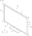
- Fig. 1 is a perspective view illustrating a display device according to an embodiment of the present disclosure
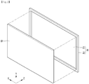
- Fig. 2 is a view illustrating a display panel and a module cover
- Fig. 3 is a rear perspective view illustrating a display device according to an embodiment of the present disclosure
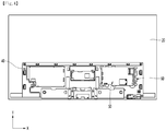
- Fig. 4 is a rear view illustrating a state where a back cover illustrated in Fig. 3 is removed.
- a display device may include a display module 1, a stand 1A supporting the display module 1 from below, and a back cover 30 located at the rear of the display module 1.
- the display module 1 may have a substantially rectangular plate shape.
- the display module 1 may include a first long side LS1, a second long side LS2 facing the first long side LS1, a first short side SS1 adjacent to one ends of the first long side LS1 and the second long side LS2, and a second short side SS2 facing the first short side SS1.
- the first long side LS1, the second long side LS2, the first short side SS1, and the second short side SS2 may mean an upper side, a lower side, a left side, and a right side of the display module 1, respectively.
- the lengths of the first and second long sides LS1 and LS2 may be formed longer than the lengths of the first and second short sides SS1 and SS2 but are not limited thereto, and the lengths of the first and second long sides LS1 and LS2 also possible to be approximately the same as the lengths of the first and second short sides SS1 and SS2.
- a point where the first long side LS1, the second long side LS2, the first short side SS1, and the second short side SS2 meet each other may be referred to as a corner.
- the point where the first long side LS1 and the first short side SS1 meet can be referred to as a first corner C1
- the point where the first long side LS1 and the second short side SS2 can be referred to as a second corner C2
- the point where the second short side SS2 and the second long side LS2 meet can be referred to as a third corner C3
- the point where the second long side LS2 and the first short side SS1 meet can be referred to as a fourth corner C4.
- the display module 1 may be supported by the stand 1A.
- the stand 1A may support the display module 1 at the bottom of the display module 1.
- the display module 1 may include a display panel 10 that displays an image, and a module cover 20 that covers the display panel 10 from the rear.
- the display panel 10 may be an OLED panel.
- the display panel 10 may display an image forward.
- the module cover 20 may be configured as a square frame.
- the module cover 20 may include a cover main body 20B (see Fig. 7 ) made of a metal material, and a coating layer 20C (see Fig. 7 ) coated on the surface of the cover main body 20B.
- the insulation resistance of the coating layer 20C may be greater than the insulation resistance of the cover main body 20B.
- the module cover 20 may be made of a PreCoated Metal (PCM) material.
- PCM PreCoated Metal
- the module cover 20 may include a cover body 21 located at the rear of the display panel 10 and a cover circumference part 22 protruding forward from the circumference of the cover body 21 and surrounding the outer circumference of the display panel 10.
- the module cover 20 may further include a heat dissipation plate (not illustrated) attached to the rear surface of the display panel 10 in a front and rear direction.
- An electrical mounting part 40 may be formed on the rear surface of the module cover 20.
- the electrical mounting part 40 may be formed on the rear surface of the cover body 21.
- the electrical mounting part 40 may be formed as a separate member from the module cover 20 and fastened to the module cover 20, or the module cover 20 may be molded and formed integrally with the module cover 20.
- SB system board
- PS power supply
- the power supply (PS) may convert commercial AC power into driving power of the system board (SB) and the display panel 10 driving circuit.
- the system board (SB) may supply DC input power from the power supply (PS) to the display panel 10 driving circuit and transmit an image signal and a timing signal synchronized with the image signal to the display panel 10 driving circuit.
- System board may be a system board for various display applications such as a television system, a set-top box, a navigation system, a DVD player, a Blu-ray player, a personal computer (PC), a home theater system, a phone system, a vehicle control system, or the like.
- display applications such as a television system, a set-top box, a navigation system, a DVD player, a Blu-ray player, a personal computer (PC), a home theater system, a phone system, a vehicle control system, or the like.
- the system board (SB) may include the PCB 50.
- the PCB 50 may include a tuner that receives a broadcast signal, an external device interface connected to an external device, a user interface device that receives a user input, various sensors, or the like.
- Side brackets 60 may be connected to the side of the PCB 50.
- the side bracket 60 may be fastened 50 to the electrical mounting part 40 of the module cover 20 together with the PCB.
- the back cover 30 may cover the electrical mounting part 40 and the electrical part such as the PCB 50 mounted on the electrical mounting part 40 from the rear.
- the back cover 30 may be fastened to the rear surface of the module cover 20.
- Fig. 5 is a view illustrating a state where a PCB and a side bracket are separated from a module cover according to an embodiment of the present disclosure
- Fig. 6 is a view for explaining a state where the PCB and the side bracket illustrated in Fig. 5 are restricted to the module cover by a restriction member
- Fig. 7 is a sectional view illustrating a state where a PCB and a side bracket are restricted to a module cover by a restriction member according to an embodiment of the present disclosure
- Fig. 8 is an enlarged view illustrating a fixing recess of a PCB and a PCB connector of a side bracket
- Fig. 9 is a rear view illustrating a PCB and a side bracket according to an embodiment of the present disclosure.
- the PCB 50 and the side bracket 60 may be mounted on the rear surface of the module cover 20.
- the PCB 50 and the side bracket 60 may be fastened to the electrical mounting part 40 formed on the rear surface of the module cover 20.
- a protrusion 41 which protrudes toward the rear and is in contact with the PCB 50 may be formed on the electric mounting part 40.
- the protrusion 41 may be in contact with the front surface of the PCB 50 and support the PCB 50 in the front and rear direction.
- a fastening hole 42 may be formed in the protrusion 41.
- the fastening hole 42 may be formed by penetrating the protrusion 41 in the front and rear direction.
- a female thread may be formed in the inner circumference of the fastening hole 42.
- the fastening portion 72 of the restriction member 70 to be described later may be inserted into the fastening hole 42 to be fastened.
- the PCB 50 may be mounted on the rear surface of the cover module 20.
- the PCB 50 may be mounted on the electrical mounting part 40 formed on the rear surface of the cover module 20.
- the rear surface 50A of the PCB 50 may face the inner surface of the back cover 30, and the front surface 50B thereof may be in contact with the protrusion 41 formed on the electrical mounting part 40.
- the PCB 50 may be provided with a number of terminals and devices.
- a plurality of input/output terminals 54 may be provided on a side edge of the rear surface 50A of the PCB 50.
- a connector such as a cable or an electric wire may be connected to each input/output terminal 54.
- Each input/output terminal 54 may be inserted into a terminal hole 61A (see Fig. 10 ) formed on the side bracket 60 or located at a point corresponding to the terminal hole 61A, and the connector may be connected to the input/output terminal 54 through a terminal hole 61A.
- the PCB 50 may be in contact with the coating layer 20C of the module cover 20.
- the front surface 50B of the PCB 50 may be in contact with the coating layer 20C of the module cover 20. Since the insulation resistance of the coating layer is relatively high, the PCB 50 may not be grounded or may be poorly grounded even when the PCB 50 is in contact with the coating layer C.
- a fixing recess 51 may be formed on the PCB 50.
- the fixing recess 51 may be formed on the upper edge and the lower edge of the PCB 50, respectively.
- the position of the fixing recess 51 is not limited thereto and may be changed as necessary.
- the fastening portion 72 of the restriction member 70 may be positioned in the fixing recess 51. In other words, the fastening portion 72 of the restriction member 70 may pass through the fixing recess 51 and be fastened to the fastening hole 42.
- a fixing piece 62B to be described later may be inserted into the fixing recess 51.
- the fastening portion 72 of the restriction member 70 may pass between the inner circumference of the fixing recess 51 and the fixing piece 62B and be fastened to the fastening hole 42 of the protrusion 41.
- the side bracket 60 may be connected to the side of the PCB 50.
- the side bracket 60 may be restricted to the rear surface of the module cover 20 together with the PCB 50 by the restriction member 70.
- the side bracket 60 may be restricted to the electrical mounting part 40.
- the side bracket 60 may be long disposed in the vertical direction.
- the length of the side brackets 60 in the vertical direction may be equal to or longer than the length of the PCB 50 in the vertical direction.
- the side bracket 60 may be made of insulating material.
- the side bracket 60 may be an injection mold product.
- the side bracket 60 may include a bracket body 61 on which a terminal hole 61A (see Fig. 10 ) is formed, and a PCB connector 62 protruding from the bracket body 61.
- the bracket body 61 may have a predetermined width in the front and rear direction. At least one terminal hole 61A may be formed through the bracket body 61 in the left and right direction.
- the PCB connector 62 may protrude from the bracket body 61.
- the PCB connector 62 may protrude laterally from the upper and lower ends of the bracket body 61.
- the PCB connector 62 may be in contact with the PCB 50 to fix the PCB 50.
- the PCB connector 62 may be restricted by the restriction member 70.
- the PCB connector 62 may include a contact portion 62A which is in contact with the PCB 50 and a fixing piece 62B connected to the contact portion 62A.
- the contact portion 62A may protrude from the bracket body 61.
- the contact portion 62A may be in contact with the rear surface 50A of the PCB 50.
- An open hole 65 may be formed in the contact portion 62A.
- the open hole 65 may be passed through the contact portion in the front and rear direction.
- the head portion 71 of the restriction member 70 may be located in the open hole 65.
- the shape of the open hole 56 is not limited.
- the size of the open hole 65 may be larger than the size of the head portion 71 of the restriction member 70. Accordingly, the head portion 71 is located in the open hole 65 and may be in contact with the PCB 50.
- the inner circumference of the open hole 65 may surround at least a portion of the outer circumference of the head portion 71 of the restriction member 70.
- the outer circumference of the head portion 71 and the inner circumference of the opening hole 65 may be spaced apart from each other.
- the fixing piece 62B may be connected to the contact portion 62A.
- the fixing piece 62B may protrude from the contact portion 62A and then extend toward the radially inward direction of the opening hole 65.
- the fixing piece 62B may be inserted and fitted into the fixing recess 51 formed on the PCB 50. Accordingly, the PCB connector 62 of the side bracket 60 may be firmly connected to the PCB 50.
- the fastening portion 72 of the restriction member 70 may pass between the inner circumference of the fixing recess 51 and the fixing piece 62B.
- the fixing recess 51 may include an inner region through which the fastening portion 72 of the restriction member 70 passes, and an outer region positioned outside the inner region and into which the fixing piece 62B is inserted.
- the inner region may communicate with the fastening hole 42 of the module cover 20.
- the head portion 71 of the restriction member 70 may cover the inner region and at least a portion of the fixing piece 62B.
- the fixing piece 62B may be fixed between the head portion 71 of the restriction member 70 and the protrusion 41 of the module cover 20 in the front and rear direction. Accordingly, the side bracket 60 may be restricted in the front and rear direction.
- restriction member 70 may restrict the PCB 50 and the side bracket 60 to the module cover 20 and ground the PCB 50 to the module cover 20.
- the restriction member 70 may be a bolt or screw.
- the restriction member 70 may be made of a metal material and current may be energized to the restriction member.
- the restriction member 70 may include a head portion 71 that is in contact with the PCB 50 and restricts the side bracket 60, and a fastening portion 72 that extends from the head portion 71 and is fastened to the module cover 20.
- At least a portion of the head portion 71 may be located in an open hole 65 formed in the PCB connector 62 of the side bracket 60.
- the head portion 71 may be in contact with the PCB 50 and the fixing piece 62B.
- the head portion 71 may include a first region 71A which is in contact with the PCB 50, and a second region 71B which is in contact with the fixing piece 62B.
- the area of the first region 71A may be wider than the area of the second region 71B.
- the fastening portion 72 may extend forward from the head portion 71.
- the fastening portion 72 may pass through the fixing recess 51 of the PCB 50 to be fastened to the fastening hole 42 of the module cover 20.
- the fastening portion 72 is fastened to the fastening hole 42 so that the fastening portion 72 may be in contact with the cover main body 20B of the module cover 20.
- the head portion 71 of the restriction member 70 may be in contact with the PCB 50 and the fastening portion 72 may be in contact with the cover main body 20B made of a metal material. Accordingly, the PCB 50 can be grounded to the cover main body 20B of the module cover 20 through the restriction member 70, and the cover main body 20B can function as a ground. Accordingly, electromagnetic interference (EMI) due to the PCB 50 may be reduced.
- EMI electromagnetic interference
- Fig. 10 is a perspective view illustrating a side bracket according to an embodiment of the present disclosure
- Fig. 11 is a perspective view illustrating the side bracket illustrated in Fig. 10 viewed from a different direction
- Fig. 12 is an enlarged view illustrating a periphery of a latch of the side bracket
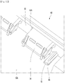
- Fig. 13 is an enlarged view illustrating a periphery of a rib of the side bracket.
- the side bracket 60 may include a bracket body 61 on which a terminal hole 61A is formed, and a PCB connector 62 protruding from the bracket body 61.
- the side bracket 60 may further include a module cover fastening portion 63 connected to the bracket body 61 and fastened to the module cover 20.
- the module cover fastening portion 63 may have a shape bent in the bracket body 61.
- the module cover fastening portion 63 may have a predetermined width in the left and right direction.
- At least one through-hole is formed on the module cover fastening portion 63, and a fastening member (not illustrated) such as a screw passes through the through-hole to be capable of being fastened to the rear surface of the module cover 20, in more detail, to the electrical mounting part 40.
- the module cover fastening portion 63 and the PCB connector 62 may be located opposite to each other with respect to the bracket body 61.
- the side bracket 60 may further include at least one of a latch 66 protruding from the bracket body 61 and connected to the PCB 50 and a rib 67 protruding from the bracket body 61 and supporting the PCB 50.
- a case where the side bracket 60 includes both the latch 66 and the rib 67 will be described as an example.
- the latch 66 and the rib 67 may be located on the opposite side of the module cover fastening portion 63 with respect to the bracket body 61.
- the latch 66 and the rib 67 may protrude from the bracket body 61 in a direction parallel to the PCB connector 62.
- the latch 66 and the rib 67 can temporarily fix the side bracket 60 to the PCB 50.
- the side bracket 60 may be restricted to the cover module 20 by the restriction member 70 in a state of being temporarily fixed to the PCB 50 by the latch 66 and the rib 67.
- the latch 66 may be fixed by being caught in a locking hole 55 formed through the PCB 50 in the front and rear direction. Accordingly, the latch 66 may temporarily fix the side bracket 60 to the PCB 50 in the left and right direction and the vertical direction.
- the rib 67 may support the PCB 50 by being in contact with the PCB 50.
- the rib 67 may guide the PCB 50 at the time of connection of the PCB 50 and the side bracket 60.
- the latch 66 and the rib 67 may be located opposite to each other with respect to the PCB 50.
- the latch 66 may be connected to any one of the front surface 50B and the rear surface 50A of the PCB 50, and the rib 67 may support the other one of the front surface 50B and the rear surface 50A of the PCB 50.
- the latch 66 may be connected to the rear surface 50A of the PCB 50, and the rib may support the front surface 50B of the PCB 50.
- the PCB 50 can be fixed between the latch 66 and the rib 67 in the front and rear direction.
- Fig. 14 is a sectional view illustrating a state where a PCB and a side bracket are restricted to a module cover by a restriction member according to another embodiment of the present disclosure.
- the head portion 71' of the restriction member 70' may include a small-diameter portion 71C which is in contact with the PCB 50 and a large-diameter portion 71D which has a diameter larger than the small-diameter portion 71C and restricts the side bracket 60.
- the fastening portion 72 may be formed to extend from the small-diameter portion 71C.
- the large-diameter portion 71D may be formed at the rear of the small-diameter portion 71C, and the fastening portion 72 may extend forward from the small-diameter portion 71C.
- the small-diameter portion 71C is located in the open hole 65 and can be in contact with the PCB 50, and the large-diameter portion 71D is located outside the open hole 65 and can be in contact with the PCB connector 62'.
- the large-diameter portion 71D and the small-diameter portion 71C may be formed to be stepped from each other. However, it is not limited thereto, and, of course, a configuration in which the diameter gradually decreases from the large-diameter portion to the small-diameter portion is also possible.
- the PCB connector 62' of the side bracket 60 may be restricted between the large-diameter portion 71D and the PCB 50 in the front and rear direction.
- the PCB connector 62' according to the present embodiment can be firmly fastened to the PCB 50 without including the fixing piece 62B (see Fig. 9 ), and the fixing hole 51' instead of the fixing recess in the PCB 50 can be formed.
- the fastening portion 72 of the restriction member 70' may pass through the fixing hole 51' to be fastened to the fastening hole 42 of the cover module 20.
Landscapes
- Engineering & Computer Science (AREA)
- Physics & Mathematics (AREA)
- Theoretical Computer Science (AREA)
- General Physics & Mathematics (AREA)
- Nonlinear Science (AREA)
- General Engineering & Computer Science (AREA)
- Computer Hardware Design (AREA)
- Human Computer Interaction (AREA)
- Mathematical Physics (AREA)
- Chemical & Material Sciences (AREA)
- Crystallography & Structural Chemistry (AREA)
- Optics & Photonics (AREA)
- Power Engineering (AREA)
- Microelectronics & Electronic Packaging (AREA)
- Electromagnetism (AREA)
- Devices For Indicating Variable Information By Combining Individual Elements (AREA)
- Casings For Electric Apparatus (AREA)
Abstract
Description
- The present disclosure relates to a display device, and more particularly, to a display device including a PCB and a side bracket.
- A display device includes a liquid crystal display (LCD), a field emission display (FED), a plasma display panel (PDP), an electroluminescence device, or the like.
- As an example of the electroluminescence device, an organic light-emitting display device of an active matrix type using an organic light-emitting diode (OLED) is commercially available. Since the organic light-emitting display device is a self-luminous device, the organic light-emitting display device has no backlight compared to the liquid crystal display, and has advantages in response speed, a viewing angle, or the like and thus is attracting attention as a next-generation display device.
- The display device includes a display panel on which an image is displayed, and a module cover covering an outer circumference and a rear surface of the display panel.
- In a conventional display device, since the module cover is metal, a PCB such as a main board can be in contact with the module cover and function as a ground for the PCB. In other words, as the PCB is directly in contact with the module cover and is grounded, electromagnetic interference (EMI) could be reduced.
- However, in recent years, there is a trend of changing the design of the module cover to form a portion of an outer appearance of the display device, and accordingly, a coating layer is formed on the surface of the module cover. Therefore, even if the PCB is in contact with the module cover, there was a problem that the grounding performance of the module cover was deteriorated due to the coating layer, and to solve this problem, a method of using a separate conductive tape (EMI Tape) was devised, but there is a problem additional cost occurs, the manufacturing process thereof becomes complicated, and it is difficult to ensure uniform quality so that the reliability of the grounding deteriorates.
- One problem to be solved by the present disclosure is to provide a display device with improved EMI due to a PCB while using a module cover including a coating layer having high insulation resistance on the surface thereof.
- Another problem to be solved by the present disclosure is to provide a display device in which a PCB is grounded to a module cover by a restriction member that restricts the PCB and the side bracket.
- A display device according to the present disclosure may include a display panel, a module cover disposed behind the display panel, a PCB mounted on a rear surface of the module cover, a side bracket connected to a side of the PCB and restricted by the rear surface of the module cover, and a restriction member restricting the PCB and the side bracket to the module cover and grounding the PCB to the module cover. The restriction member may include a head portion which is in contact with the PCB and restricts the side bracket, and a fastening portion extending from the head portion and fastened to the module cover.
- The module cover may include a cover main body which is made of metal and in contact with the fastening portion, and a coating layer which is coated on a surface of the cover main body, has an insulation resistance higher than that of the cover main body, and is in contact with the PCB.
- The side bracket may include a bracket body having a terminal hole corresponding to a terminal provided in the PCB, and a PCB connector protruding from the bracket body and restricted by the head portion.
- A fixing recess in which a portion of the fastening portion is located may be formed in the PCB.
- The PCB connector may include a contact portion which has an open hole larger than the head portion and is in contact with the PCB, and a fixing piece which is connected to the contact portion and inserted into the fixing recess.
- The head portion may include a first region which is in contact with the PCB; and a second region which is in contact with the fixing piece.
- An area of the first region may be wider than an area of the second region.
- At least a portion of an outer circumference of the head portion may be surrounded by an inner circumference of the opening hole.
- The side bracket may further include at least one of a latch protruding from the bracket body and connected to the PCB and a rib protruding from the bracket body and supporting the PCB.
- The side bracket may include a latch protruding from the bracket body and connected to one of a front surface and a rear surface of the PCB, and a rib protruding from the bracket body and supporting the other of the front surface and the rear surface of the PCB.
- The module cover may be made of PCM material.
- The head portion may include a small-diameter portion which is in contact with the PCB; and a large-diameter portion having a larger diameter than the small-diameter portion and restricting the side bracket.
- According to a preferred embodiment of the present disclosure, since the PCB can be grounded to the module cover by the restriction member, EMI caused due to the PCB can be improved.
- In addition, since the cover module forming the outer appearance of the display device includes a coating layer having high insulation resistance, the safety of the display device can be improved, and the outer appearance of the display device can be improved in design.
- In addition, compared to a case where the PCB is grounded with the module cover using a separate subsidiary material such as a conductive tape, the cost is reduced, the manufacturing process is simplified, and the reliability of grounding is improved by securing uniform quality.
- In addition, the side bracket can be temporarily fixed to the PCB by the latch and rib of the side bracket. Accordingly, since the restriction member can be fastened to the module cover while the side bracket and the PCB are temporarily fixed, ease of assembly can be improved.
- In addition, since the fixing piece is fitted and fixed in the fixing recess of the PCB, and the fixing piece is restricted by the restriction member, the connection between the PCB and the side bracket can be solid.
-
-
Fig. 1 is a perspective view illustrating a display device according to an embodiment of the present disclosure. -
Fig. 2 is a view illustrating a display panel and a module cover. -
Fig. 3 is a rear perspective view illustrating a display device according to an embodiment of the present disclosure. -
Fig. 4 is a rear view illustrating a state where a back cover illustrated inFig. 3 is removed. -
Fig. 5 is a view illustrating a state where a PCB and a side bracket are separated from a module cover according to an embodiment of the present disclosure. -
Fig. 6 is a view for explaining a state where the PCB and the side bracket illustrated inFig. 5 are restricted to the module cover by a restriction member. -
Fig. 7 is a sectional view illustrating a state where a PCB and a side bracket are restricted to a module cover by a restriction member according to an embodiment of the present disclosure. -
Fig. 8 is an enlarged view illustrating a fixing recess of a PCB and a PCB connector of a side bracket. -
Fig. 9 is a rear view illustrating a PCB and a side bracket according to an embodiment of the present disclosure. -
Fig. 10 is a perspective view illustrating a side bracket according to an embodiment of the present disclosure. -
Fig. 11 is a perspective view illustrating the side bracket illustrated inFig. 10 viewed in a different direction. -
Fig. 12 is an enlarged view illustrating a periphery of a latch of the side bracket. -
Fig. 13 is an enlarged view illustrating a periphery of a rib of the side bracket. -
Fig. 14 is a sectional view illustrating a state where a PCB and a side bracket are restricted to a module cover by a restriction member according to another embodiment of the present disclosure. - Hereinafter, specific embodiments of the present disclosure will be described in detail together with the drawings.
-
Fig. 1 is a perspective view illustrating a display device according to an embodiment of the present disclosure,Fig. 2 is a view illustrating a display panel and a module cover,Fig. 3 is a rear perspective view illustrating a display device according to an embodiment of the present disclosure, andFig. 4 is a rear view illustrating a state where a back cover illustrated inFig. 3 is removed. - A display device according to an embodiment of the present disclosure may include a
display module 1, astand 1A supporting thedisplay module 1 from below, and aback cover 30 located at the rear of thedisplay module 1. - The
display module 1 may have a substantially rectangular plate shape. In more detail, thedisplay module 1 may include a first long side LS1, a second long side LS2 facing the first long side LS1, a first short side SS1 adjacent to one ends of the first long side LS1 and the second long side LS2, and a second short side SS2 facing the first short side SS1. - The first long side LS1, the second long side LS2, the first short side SS1, and the second short side SS2 may mean an upper side, a lower side, a left side, and a right side of the
display module 1, respectively. - The lengths of the first and second long sides LS1 and LS2 may be formed longer than the lengths of the first and second short sides SS1 and SS2 but are not limited thereto, and the lengths of the first and second long sides LS1 and LS2 also possible to be approximately the same as the lengths of the first and second short sides SS1 and SS2.
- In addition, a point where the first long side LS1, the second long side LS2, the first short side SS1, and the second short side SS2 meet each other may be referred to as a corner. For example, the point where the first long side LS1 and the first short side SS1 meet can be referred to as a first corner C1, the point where the first long side LS1 and the second short side SS2 can be referred to as a second corner C2, the point where the second short side SS2 and the second long side LS2 meet can be referred to as a third corner C3, and the point where the second long side LS2 and the first short side SS1 meet can be referred to as a fourth corner C4.
- The
display module 1 may be supported by thestand 1A. Thestand 1A may support thedisplay module 1 at the bottom of thedisplay module 1. - The
display module 1 may include adisplay panel 10 that displays an image, and amodule cover 20 that covers thedisplay panel 10 from the rear. - The
display panel 10 may be an OLED panel. Thedisplay panel 10 may display an image forward. - The
module cover 20 may be configured as a square frame. Themodule cover 20 may include a covermain body 20B (seeFig. 7 ) made of a metal material, and acoating layer 20C (seeFig. 7 ) coated on the surface of the covermain body 20B. The insulation resistance of thecoating layer 20C may be greater than the insulation resistance of the covermain body 20B. - For example, the
module cover 20 may be made of a PreCoated Metal (PCM) material. - The
module cover 20 may include acover body 21 located at the rear of thedisplay panel 10 and acover circumference part 22 protruding forward from the circumference of thecover body 21 and surrounding the outer circumference of thedisplay panel 10. Themodule cover 20 may further include a heat dissipation plate (not illustrated) attached to the rear surface of thedisplay panel 10 in a front and rear direction. - An electrical mounting
part 40 may be formed on the rear surface of themodule cover 20. In more detail, the electrical mountingpart 40 may be formed on the rear surface of thecover body 21. The electrical mountingpart 40 may be formed as a separate member from themodule cover 20 and fastened to themodule cover 20, or themodule cover 20 may be molded and formed integrally with themodule cover 20. - Electrical components such as a system board (SB) and a power supply (PS) may be mounted on the electrical mounting
part 40. - The power supply (PS) may convert commercial AC power into driving power of the system board (SB) and the
display panel 10 driving circuit. The system board (SB) may supply DC input power from the power supply (PS) to thedisplay panel 10 driving circuit and transmit an image signal and a timing signal synchronized with the image signal to thedisplay panel 10 driving circuit. - System board (SB) may be a system board for various display applications such as a television system, a set-top box, a navigation system, a DVD player, a Blu-ray player, a personal computer (PC), a home theater system, a phone system, a vehicle control system, or the like.
- The system board (SB) may include the
PCB 50. ThePCB 50 may include a tuner that receives a broadcast signal, an external device interface connected to an external device, a user interface device that receives a user input, various sensors, or the like. -
Side brackets 60 may be connected to the side of thePCB 50. Theside bracket 60 may be fastened 50 to the electrical mountingpart 40 of themodule cover 20 together with the PCB. - Meanwhile, the
back cover 30 may cover the electrical mountingpart 40 and the electrical part such as thePCB 50 mounted on the electrical mountingpart 40 from the rear. Theback cover 30 may be fastened to the rear surface of themodule cover 20. -
Fig. 5 is a view illustrating a state where a PCB and a side bracket are separated from a module cover according to an embodiment of the present disclosure,Fig. 6 is a view for explaining a state where the PCB and the side bracket illustrated inFig. 5 are restricted to the module cover by a restriction member,Fig. 7 is a sectional view illustrating a state where a PCB and a side bracket are restricted to a module cover by a restriction member according to an embodiment of the present disclosure,Fig. 8 is an enlarged view illustrating a fixing recess of a PCB and a PCB connector of a side bracket, andFig. 9 is a rear view illustrating a PCB and a side bracket according to an embodiment of the present disclosure. - The
PCB 50 and theside bracket 60 may be mounted on the rear surface of themodule cover 20. In more detail, thePCB 50 and theside bracket 60 may be fastened to the electrical mountingpart 40 formed on the rear surface of themodule cover 20. - A
protrusion 41 which protrudes toward the rear and is in contact with thePCB 50 may be formed on the electric mountingpart 40. Theprotrusion 41 may be in contact with the front surface of thePCB 50 and support thePCB 50 in the front and rear direction. - A
fastening hole 42 may be formed in theprotrusion 41. Thefastening hole 42 may be formed by penetrating theprotrusion 41 in the front and rear direction. A female thread may be formed in the inner circumference of thefastening hole 42. Thefastening portion 72 of therestriction member 70 to be described later may be inserted into thefastening hole 42 to be fastened. - The
PCB 50 may be mounted on the rear surface of thecover module 20. In more detail, thePCB 50 may be mounted on the electrical mountingpart 40 formed on the rear surface of thecover module 20. Therear surface 50A of thePCB 50 may face the inner surface of theback cover 30, and thefront surface 50B thereof may be in contact with theprotrusion 41 formed on the electrical mountingpart 40. - The
PCB 50 may be provided with a number of terminals and devices. In more detail, a plurality of input/output terminals 54 may be provided on a side edge of therear surface 50A of thePCB 50. - A connector (not illustrated) such as a cable or an electric wire may be connected to each input/
output terminal 54. Each input/output terminal 54 may be inserted into aterminal hole 61A (seeFig. 10 ) formed on theside bracket 60 or located at a point corresponding to theterminal hole 61A, and the connector may be connected to the input/output terminal 54 through aterminal hole 61A. - The
PCB 50 may be in contact with thecoating layer 20C of themodule cover 20. In more detail, thefront surface 50B of thePCB 50 may be in contact with thecoating layer 20C of themodule cover 20. Since the insulation resistance of the coating layer is relatively high, thePCB 50 may not be grounded or may be poorly grounded even when thePCB 50 is in contact with the coating layer C. - In addition, a fixing
recess 51 may be formed on thePCB 50. The fixingrecess 51 may be formed on the upper edge and the lower edge of thePCB 50, respectively. - However, the position of the fixing
recess 51 is not limited thereto and may be changed as necessary. In addition, it is also possible to form a fixing hole instead of the fixingrecess 51. - The
fastening portion 72 of therestriction member 70 may be positioned in the fixingrecess 51. In other words, thefastening portion 72 of therestriction member 70 may pass through the fixingrecess 51 and be fastened to thefastening hole 42. - In addition, a fixing
piece 62B to be described later may be inserted into the fixingrecess 51. Thefastening portion 72 of therestriction member 70 may pass between the inner circumference of the fixingrecess 51 and the fixingpiece 62B and be fastened to thefastening hole 42 of theprotrusion 41. - Meanwhile, the
side bracket 60 may be connected to the side of thePCB 50. Theside bracket 60 may be restricted to the rear surface of themodule cover 20 together with thePCB 50 by therestriction member 70. In more detail, theside bracket 60 may be restricted to the electrical mountingpart 40. - The
side bracket 60 may be long disposed in the vertical direction. The length of theside brackets 60 in the vertical direction may be equal to or longer than the length of thePCB 50 in the vertical direction. - The
side bracket 60 may be made of insulating material. Theside bracket 60 may be an injection mold product. - The
side bracket 60 may include abracket body 61 on which aterminal hole 61A (seeFig. 10 ) is formed, and aPCB connector 62 protruding from thebracket body 61. - The
bracket body 61 may have a predetermined width in the front and rear direction. At least oneterminal hole 61A may be formed through thebracket body 61 in the left and right direction. - The
PCB connector 62 may protrude from thebracket body 61. In more detail, thePCB connector 62 may protrude laterally from the upper and lower ends of thebracket body 61. - The
PCB connector 62 may be in contact with thePCB 50 to fix thePCB 50. ThePCB connector 62 may be restricted by therestriction member 70. - In more detail, the
PCB connector 62 may include acontact portion 62A which is in contact with thePCB 50 and afixing piece 62B connected to thecontact portion 62A. - The
contact portion 62A may protrude from thebracket body 61. Thecontact portion 62A may be in contact with therear surface 50A of thePCB 50. - An
open hole 65 may be formed in thecontact portion 62A. Theopen hole 65 may be passed through the contact portion in the front and rear direction. Thehead portion 71 of therestriction member 70 may be located in theopen hole 65. The shape of the open hole 56 is not limited. - The size of the
open hole 65 may be larger than the size of thehead portion 71 of therestriction member 70. Accordingly, thehead portion 71 is located in theopen hole 65 and may be in contact with thePCB 50. - The inner circumference of the
open hole 65 may surround at least a portion of the outer circumference of thehead portion 71 of therestriction member 70. The outer circumference of thehead portion 71 and the inner circumference of theopening hole 65 may be spaced apart from each other. - The fixing
piece 62B may be connected to thecontact portion 62A. The fixingpiece 62B may protrude from thecontact portion 62A and then extend toward the radially inward direction of theopening hole 65. - The fixing
piece 62B may be inserted and fitted into the fixingrecess 51 formed on thePCB 50. Accordingly, thePCB connector 62 of theside bracket 60 may be firmly connected to thePCB 50. - The
fastening portion 72 of therestriction member 70 may pass between the inner circumference of the fixingrecess 51 and the fixingpiece 62B. In other words, the fixingrecess 51 may include an inner region through which thefastening portion 72 of therestriction member 70 passes, and an outer region positioned outside the inner region and into which thefixing piece 62B is inserted. When therestriction member 70 is fastened, even if the rotational force of thehead portion 71 is transmitted to the fixingpiece 62B, the fixingpiece 62B may not be separated from the fixingrecess 51. - The inner region may communicate with the
fastening hole 42 of themodule cover 20. Thehead portion 71 of therestriction member 70 may cover the inner region and at least a portion of the fixingpiece 62B. - The fixing
piece 62B may be fixed between thehead portion 71 of therestriction member 70 and theprotrusion 41 of themodule cover 20 in the front and rear direction. Accordingly, theside bracket 60 may be restricted in the front and rear direction. - Meanwhile, the
restriction member 70 may restrict thePCB 50 and theside bracket 60 to themodule cover 20 and ground thePCB 50 to themodule cover 20. - The
restriction member 70 may be a bolt or screw. Therestriction member 70 may be made of a metal material and current may be energized to the restriction member. - The
restriction member 70 may include ahead portion 71 that is in contact with thePCB 50 and restricts theside bracket 60, and afastening portion 72 that extends from thehead portion 71 and is fastened to themodule cover 20. - At least a portion of the
head portion 71 may be located in anopen hole 65 formed in thePCB connector 62 of theside bracket 60. - The
head portion 71 may be in contact with thePCB 50 and the fixingpiece 62B. In other words, thehead portion 71 may include afirst region 71A which is in contact with thePCB 50, and asecond region 71B which is in contact with the fixingpiece 62B. The area of thefirst region 71A may be wider than the area of thesecond region 71B. - The
fastening portion 72 may extend forward from thehead portion 71. Thefastening portion 72 may pass through the fixingrecess 51 of thePCB 50 to be fastened to thefastening hole 42 of themodule cover 20. - Since the
fastening hole 42 of themodule cover 20 penetrates to the covermain body 20B, thefastening portion 72 is fastened to thefastening hole 42 so that thefastening portion 72 may be in contact with the covermain body 20B of themodule cover 20. - In other words, the
head portion 71 of therestriction member 70 may be in contact with thePCB 50 and thefastening portion 72 may be in contact with the covermain body 20B made of a metal material. Accordingly, thePCB 50 can be grounded to the covermain body 20B of themodule cover 20 through therestriction member 70, and the covermain body 20B can function as a ground. Accordingly, electromagnetic interference (EMI) due to thePCB 50 may be reduced. -
Fig. 10 is a perspective view illustrating a side bracket according to an embodiment of the present disclosure,Fig. 11 is a perspective view illustrating the side bracket illustrated inFig. 10 viewed from a different direction,Fig. 12 is an enlarged view illustrating a periphery of a latch of the side bracket, andFig. 13 is an enlarged view illustrating a periphery of a rib of the side bracket. - As described above, the
side bracket 60 may include abracket body 61 on which aterminal hole 61A is formed, and aPCB connector 62 protruding from thebracket body 61. - The
side bracket 60 may further include a modulecover fastening portion 63 connected to thebracket body 61 and fastened to themodule cover 20. - The module
cover fastening portion 63 may have a shape bent in thebracket body 61. The modulecover fastening portion 63 may have a predetermined width in the left and right direction. - At least one through-hole is formed on the module
cover fastening portion 63, and a fastening member (not illustrated) such as a screw passes through the through-hole to be capable of being fastened to the rear surface of themodule cover 20, in more detail, to the electrical mountingpart 40. - The module
cover fastening portion 63 and thePCB connector 62 may be located opposite to each other with respect to thebracket body 61. - Meanwhile, the
side bracket 60 may further include at least one of alatch 66 protruding from thebracket body 61 and connected to thePCB 50 and arib 67 protruding from thebracket body 61 and supporting thePCB 50. Hereinafter, a case where theside bracket 60 includes both thelatch 66 and therib 67 will be described as an example. - The
latch 66 and therib 67 may be located on the opposite side of the modulecover fastening portion 63 with respect to thebracket body 61. Thelatch 66 and therib 67 may protrude from thebracket body 61 in a direction parallel to thePCB connector 62. - The
latch 66 and therib 67 can temporarily fix theside bracket 60 to thePCB 50. Theside bracket 60 may be restricted to thecover module 20 by therestriction member 70 in a state of being temporarily fixed to thePCB 50 by thelatch 66 and therib 67. - The
latch 66 may be fixed by being caught in alocking hole 55 formed through thePCB 50 in the front and rear direction. Accordingly, thelatch 66 may temporarily fix theside bracket 60 to thePCB 50 in the left and right direction and the vertical direction. - The
rib 67 may support thePCB 50 by being in contact with thePCB 50. Therib 67 may guide thePCB 50 at the time of connection of thePCB 50 and theside bracket 60. - The
latch 66 and therib 67 may be located opposite to each other with respect to thePCB 50. Thelatch 66 may be connected to any one of thefront surface 50B and therear surface 50A of thePCB 50, and therib 67 may support the other one of thefront surface 50B and therear surface 50A of thePCB 50. For example, thelatch 66 may be connected to therear surface 50A of thePCB 50, and the rib may support thefront surface 50B of thePCB 50. - Accordingly, the
PCB 50 can be fixed between thelatch 66 and therib 67 in the front and rear direction. -
Fig. 14 is a sectional view illustrating a state where a PCB and a side bracket are restricted to a module cover by a restriction member according to another embodiment of the present disclosure. - Hereinafter, contents overlapping with the above-described contents will be omitted, and the differences will be mainly described.
- The head portion 71' of the restriction member 70' according to the present embodiment may include a small-
diameter portion 71C which is in contact with thePCB 50 and a large-diameter portion 71D which has a diameter larger than the small-diameter portion 71C and restricts theside bracket 60. - The
fastening portion 72 may be formed to extend from the small-diameter portion 71C. In more detail, the large-diameter portion 71D may be formed at the rear of the small-diameter portion 71C, and thefastening portion 72 may extend forward from the small-diameter portion 71C. - The small-
diameter portion 71C is located in theopen hole 65 and can be in contact with thePCB 50, and the large-diameter portion 71D is located outside theopen hole 65 and can be in contact with the PCB connector 62'. - The large-
diameter portion 71D and the small-diameter portion 71C may be formed to be stepped from each other. However, it is not limited thereto, and, of course, a configuration in which the diameter gradually decreases from the large-diameter portion to the small-diameter portion is also possible. - Accordingly, the PCB connector 62' of the
side bracket 60 may be restricted between the large-diameter portion 71D and thePCB 50 in the front and rear direction. - Therefore, the PCB connector 62' according to the present embodiment can be firmly fastened to the
PCB 50 without including the fixingpiece 62B (seeFig. 9 ), and the fixing hole 51' instead of the fixing recess in thePCB 50 can be formed. Thefastening portion 72 of the restriction member 70' may pass through the fixing hole 51' to be fastened to thefastening hole 42 of thecover module 20. - The above description is merely illustrative of the technical idea of the present disclosure, and a person skill in the art to which the present disclosure pertains will be able to make various modifications and variations without departing from the essential characteristics of the present disclosure.
- Accordingly, the embodiments disclosed in the present disclosure are not intended to limit the technical idea of the present disclosure, but to explain the technical idea, and the scope of the technical idea of the present disclosure is not limited by these embodiments.
- The scope of protection of the present disclosure should be interpreted by the following claims, and all technical ideas within the scope equivalent thereto should be construed as being included in the scope of the present disclosure.
[Explanation of Referene Numeral] 10: display panel 120: module cover 20B: cover main body 20C: coating layer 40: electrical mounting part 42: fastening hole 50: PCB 51: fixing recess 60: side bracket 61: bracket body 62: PCB connector 62A: contact portion 62B: fixing piece 65: open hole 66: latch 67: rib 70: restriction member 71: head portion 72: fastening portion
Claims (12)
- A display device comprising:a display panel;a module cover disposed behind the display panel;a PCB mounted on a rear surface of the module cover;a side bracket connected to a side of the PCB and restricted by the rear surface of the module cover; anda restriction member restricting the PCB and the side bracket to the module cover and grounding the PCB to the module cover,wherein the restriction member includesa head portion which is in contact with the PCB and restricts the side bracket; anda fastening portion extending from the head portion and fastened to the module cover.
- The display device of claim 1,
wherein the module cover includesa cover main body which is made of metal and in contact with the fastening portion; anda coating layer which is coated on a surface of the cover main body, has an insulation resistance higher than that of the cover main body, and is in contact with the PCB. - The display device of claim 1,
wherein the side bracket includesa bracket body having a terminal hole corresponding to a terminal provided in the PCB; anda PCB connector protruding from the bracket body and restricted by the head portion. - The display device of claim 3,
wherein a fixing recess in which a portion of the fastening portion is located is formed in the PCB. - The display device of claim 4,
wherein the PCB connector includesa contact portion which has an open hole larger than the head portion and is in contact with the PCB; anda fixing piece which is connected to the contact portion and inserted into the fixing recess. - The display device of claim 5,
wherein the head portion includesa first region which is in contact with the PCB; anda second region which is in contact with the fixing piece. - The display device of claim 6,
wherein an area of the first region is wider than an area of the second region. - The display device of claim 5,
wherein at least a portion of an outer circumference of the head portion is surrounded by an inner circumference of the opening hole. - The display device of claim 3,
wherein the side bracket further includes at least one of a latch protruding from the bracket body and connected to the PCB; and
a rib protruding from the bracket body and supporting the PCB. - The display device of claim 3,
wherein the side bracket includesa latch protruding from the bracket body and connected to one of a front surface and a rear surface of the PCB; anda rib protruding from the bracket body and supporting the other of the front surface and the rear surface of the PCB. - The display device of claim 1,
wherein the module cover is made of PCM material. - The display device of claim 1,
wherein the head portion includesa small-diameter portion which is in contact with the PCB; anda large-diameter portion having a larger diameter than the small-diameter portion and restricting the side bracket.
Applications Claiming Priority (2)
| Application Number | Priority Date | Filing Date | Title |
|---|---|---|---|
| KR1020180088175A KR102545157B1 (en) | 2018-07-27 | 2018-07-27 | Display divice |
| PCT/KR2018/015065 WO2020022581A1 (en) | 2018-07-27 | 2018-11-30 | Display apparatus |
Publications (4)
| Publication Number | Publication Date |
|---|---|
| EP3832382A1 true EP3832382A1 (en) | 2021-06-09 |
| EP3832382A4 EP3832382A4 (en) | 2022-03-09 |
| EP3832382C0 EP3832382C0 (en) | 2025-01-29 |
| EP3832382B1 EP3832382B1 (en) | 2025-01-29 |
Family
ID=69181820
Family Applications (1)
| Application Number | Title | Priority Date | Filing Date |
|---|---|---|---|
| EP18927456.6A Active EP3832382B1 (en) | 2018-07-27 | 2018-11-30 | Display device |
Country Status (4)
| Country | Link |
|---|---|
| US (1) | US11379018B2 (en) |
| EP (1) | EP3832382B1 (en) |
| KR (1) | KR102545157B1 (en) |
| WO (1) | WO2020022581A1 (en) |
Families Citing this family (3)
| Publication number | Priority date | Publication date | Assignee | Title |
|---|---|---|---|---|
| WO2021210691A1 (en) | 2020-04-13 | 2021-10-21 | 엘지전자 주식회사 | Display device |
| KR102833944B1 (en) | 2020-09-11 | 2025-07-11 | 엘지디스플레이 주식회사 | Display device |
| KR102767729B1 (en) * | 2022-06-03 | 2025-02-12 | 엘지전자 주식회사 | Display device |
Family Cites Families (8)
| Publication number | Priority date | Publication date | Assignee | Title |
|---|---|---|---|---|
| KR100490533B1 (en) | 2000-04-28 | 2005-05-17 | 삼성에스디아이 주식회사 | Plasma display apparatus where electromagenetic interference is reduced |
| KR100471064B1 (en) * | 2002-06-11 | 2005-03-10 | 삼성전자주식회사 | Displaying apparatus |
| KR100463870B1 (en) * | 2002-09-03 | 2004-12-30 | 엘지.필립스 엘시디 주식회사 | Liquid crystal display device |
| KR100546708B1 (en) * | 2003-05-19 | 2006-01-26 | 엘지.필립스 엘시디 주식회사 | LCD Display |
| KR20050068460A (en) * | 2003-12-30 | 2005-07-05 | 엘지.필립스 엘시디 주식회사 | Liquid crystal display module |
| KR100879302B1 (en) | 2007-11-26 | 2009-01-19 | 삼성에스디아이 주식회사 | Plasma display device |
| KR20110076304A (en) | 2009-12-29 | 2011-07-06 | 엘지전자 주식회사 | Display device |
| KR20170061924A (en) * | 2015-11-27 | 2017-06-07 | 엘지디스플레이 주식회사 | Backlight unit and liquid crystal display device having the same |
-
2018
- 2018-07-27 KR KR1020180088175A patent/KR102545157B1/en active Active
- 2018-11-30 US US17/051,424 patent/US11379018B2/en active Active
- 2018-11-30 WO PCT/KR2018/015065 patent/WO2020022581A1/en not_active Ceased
- 2018-11-30 EP EP18927456.6A patent/EP3832382B1/en active Active
Also Published As
| Publication number | Publication date |
|---|---|
| EP3832382A4 (en) | 2022-03-09 |
| US20210223833A1 (en) | 2021-07-22 |
| EP3832382C0 (en) | 2025-01-29 |
| US11379018B2 (en) | 2022-07-05 |
| KR102545157B1 (en) | 2023-06-20 |
| EP3832382B1 (en) | 2025-01-29 |
| KR20200012639A (en) | 2020-02-05 |
| WO2020022581A1 (en) | 2020-01-30 |
Similar Documents
| Publication | Publication Date | Title |
|---|---|---|
| US8520375B2 (en) | Display apparatus | |
| EP3832382B1 (en) | Display device | |
| US10709025B2 (en) | Display device | |
| US11038295B2 (en) | Display device | |
| US10095264B2 (en) | Sound system and display device comprising it | |
| EP3125026B1 (en) | Display device | |
| CN101086827B (en) | Driving device and a liquid crystal display including the same | |
| EP3745711A1 (en) | Display device | |
| US12178028B2 (en) | Display device | |
| US10356917B2 (en) | Display device | |
| US20240431052A1 (en) | Display device | |
| US20080259542A1 (en) | Plasma display | |
| US9693126B1 (en) | Speaker assembly and display device including speaker assembly | |
| KR102514283B1 (en) | Display apparatus | |
| EP3125027B1 (en) | Display device | |
| KR100683753B1 (en) | Plasma display device | |
| CN218631182U (en) | Display module and display screen | |
| KR20240149217A (en) | Display device | |
| EP3125025B1 (en) | Display device | |
| CN213028808U (en) | Support components and display equipment | |
| KR200327982Y1 (en) | Display Apparatus | |
| US10852575B2 (en) | Display apparatus having front cover with infrared sensor | |
| KR20140003963U (en) | The Installation Structure of Monitor for Wall Hanging | |
| KR20110080407A (en) | Display Devices and Substrates for Display Devices |
Legal Events
| Date | Code | Title | Description |
|---|---|---|---|
| STAA | Information on the status of an ep patent application or granted ep patent |
Free format text: STATUS: THE INTERNATIONAL PUBLICATION HAS BEEN MADE |
|
| PUAI | Public reference made under article 153(3) epc to a published international application that has entered the european phase |
Free format text: ORIGINAL CODE: 0009012 |
|
| STAA | Information on the status of an ep patent application or granted ep patent |
Free format text: STATUS: REQUEST FOR EXAMINATION WAS MADE |
|
| 17P | Request for examination filed |
Effective date: 20201130 |
|
| AK | Designated contracting states |
Kind code of ref document: A1 Designated state(s): AL AT BE BG CH CY CZ DE DK EE ES FI FR GB GR HR HU IE IS IT LI LT LU LV MC MK MT NL NO PL PT RO RS SE SI SK SM TR |
|
| DAV | Request for validation of the european patent (deleted) | ||
| DAX | Request for extension of the european patent (deleted) | ||
| A4 | Supplementary search report drawn up and despatched |
Effective date: 20220209 |
|
| RIC1 | Information provided on ipc code assigned before grant |
Ipc: H01L 27/32 20060101ALN20220203BHEP Ipc: H01L 27/15 20060101ALN20220203BHEP Ipc: H01L 27/02 20060101ALN20220203BHEP Ipc: G06F 1/16 20060101ALN20220203BHEP Ipc: H05K 9/00 20060101ALI20220203BHEP Ipc: G02F 1/1333 20060101AFI20220203BHEP |
|
| GRAP | Despatch of communication of intention to grant a patent |
Free format text: ORIGINAL CODE: EPIDOSNIGR1 |
|
| STAA | Information on the status of an ep patent application or granted ep patent |
Free format text: STATUS: GRANT OF PATENT IS INTENDED |
|
| RIC1 | Information provided on ipc code assigned before grant |
Ipc: H10K 59/10 20230101ALN20240729BHEP Ipc: H01L 27/15 20060101ALN20240729BHEP Ipc: H01L 27/02 20060101ALN20240729BHEP Ipc: G06F 1/16 20060101ALN20240729BHEP Ipc: H05K 9/00 20060101ALI20240729BHEP Ipc: G02F 1/1333 20060101AFI20240729BHEP |
|
| INTG | Intention to grant announced |
Effective date: 20240821 |
|
| GRAS | Grant fee paid |
Free format text: ORIGINAL CODE: EPIDOSNIGR3 |
|
| GRAA | (expected) grant |
Free format text: ORIGINAL CODE: 0009210 |
|
| STAA | Information on the status of an ep patent application or granted ep patent |
Free format text: STATUS: THE PATENT HAS BEEN GRANTED |
|
| AK | Designated contracting states |
Kind code of ref document: B1 Designated state(s): AL AT BE BG CH CY CZ DE DK EE ES FI FR GB GR HR HU IE IS IT LI LT LU LV MC MK MT NL NO PL PT RO RS SE SI SK SM TR |
|
| REG | Reference to a national code |
Ref country code: GB Ref legal event code: FG4D |
|
| REG | Reference to a national code |
Ref country code: CH Ref legal event code: EP |
|
| REG | Reference to a national code |
Ref country code: DE Ref legal event code: R096 Ref document number: 602018078922 Country of ref document: DE |
|
| REG | Reference to a national code |
Ref country code: IE Ref legal event code: FG4D |
|
| U01 | Request for unitary effect filed |
Effective date: 20250219 |
|
| U07 | Unitary effect registered |
Designated state(s): AT BE BG DE DK EE FI FR IT LT LU LV MT NL PT RO SE SI Effective date: 20250225 |
|
| PG25 | Lapsed in a contracting state [announced via postgrant information from national office to epo] |
Ref country code: RS Free format text: LAPSE BECAUSE OF FAILURE TO SUBMIT A TRANSLATION OF THE DESCRIPTION OR TO PAY THE FEE WITHIN THE PRESCRIBED TIME-LIMIT Effective date: 20250429 |
|
| PG25 | Lapsed in a contracting state [announced via postgrant information from national office to epo] |
Ref country code: PL Free format text: LAPSE BECAUSE OF FAILURE TO SUBMIT A TRANSLATION OF THE DESCRIPTION OR TO PAY THE FEE WITHIN THE PRESCRIBED TIME-LIMIT Effective date: 20250129 |
|
| PG25 | Lapsed in a contracting state [announced via postgrant information from national office to epo] |
Ref country code: ES Free format text: LAPSE BECAUSE OF FAILURE TO SUBMIT A TRANSLATION OF THE DESCRIPTION OR TO PAY THE FEE WITHIN THE PRESCRIBED TIME-LIMIT Effective date: 20250129 |
|
| PG25 | Lapsed in a contracting state [announced via postgrant information from national office to epo] |
Ref country code: IS Free format text: LAPSE BECAUSE OF FAILURE TO SUBMIT A TRANSLATION OF THE DESCRIPTION OR TO PAY THE FEE WITHIN THE PRESCRIBED TIME-LIMIT Effective date: 20250529 Ref country code: NO Free format text: LAPSE BECAUSE OF FAILURE TO SUBMIT A TRANSLATION OF THE DESCRIPTION OR TO PAY THE FEE WITHIN THE PRESCRIBED TIME-LIMIT Effective date: 20250429 |
|
| PG25 | Lapsed in a contracting state [announced via postgrant information from national office to epo] |
Ref country code: HR Free format text: LAPSE BECAUSE OF FAILURE TO SUBMIT A TRANSLATION OF THE DESCRIPTION OR TO PAY THE FEE WITHIN THE PRESCRIBED TIME-LIMIT Effective date: 20250129 |
|
| PG25 | Lapsed in a contracting state [announced via postgrant information from national office to epo] |
Ref country code: GR Free format text: LAPSE BECAUSE OF FAILURE TO SUBMIT A TRANSLATION OF THE DESCRIPTION OR TO PAY THE FEE WITHIN THE PRESCRIBED TIME-LIMIT Effective date: 20250430 |
|
| PG25 | Lapsed in a contracting state [announced via postgrant information from national office to epo] |
Ref country code: SM Free format text: LAPSE BECAUSE OF FAILURE TO SUBMIT A TRANSLATION OF THE DESCRIPTION OR TO PAY THE FEE WITHIN THE PRESCRIBED TIME-LIMIT Effective date: 20250129 |
|
| PG25 | Lapsed in a contracting state [announced via postgrant information from national office to epo] |
Ref country code: CZ Free format text: LAPSE BECAUSE OF FAILURE TO SUBMIT A TRANSLATION OF THE DESCRIPTION OR TO PAY THE FEE WITHIN THE PRESCRIBED TIME-LIMIT Effective date: 20250129 |
|
| PG25 | Lapsed in a contracting state [announced via postgrant information from national office to epo] |
Ref country code: SK Free format text: LAPSE BECAUSE OF FAILURE TO SUBMIT A TRANSLATION OF THE DESCRIPTION OR TO PAY THE FEE WITHIN THE PRESCRIBED TIME-LIMIT Effective date: 20250129 |
|
| PLBE | No opposition filed within time limit |
Free format text: ORIGINAL CODE: 0009261 |
|
| STAA | Information on the status of an ep patent application or granted ep patent |
Free format text: STATUS: NO OPPOSITION FILED WITHIN TIME LIMIT |
|
| U20 | Renewal fee for the european patent with unitary effect paid |
Year of fee payment: 8 Effective date: 20251124 |
|
| 26N | No opposition filed |
Effective date: 20251030 |
|
| U1N | Appointed representative for the unitary patent procedure changed after the registration of the unitary effect |
Representative=s name: MARKS & CLERK LLP; GB |