EP3831911A1 - Composite wavelength converter - Google Patents
Composite wavelength converter Download PDFInfo
- Publication number
- EP3831911A1 EP3831911A1 EP19213887.3A EP19213887A EP3831911A1 EP 3831911 A1 EP3831911 A1 EP 3831911A1 EP 19213887 A EP19213887 A EP 19213887A EP 3831911 A1 EP3831911 A1 EP 3831911A1
- Authority
- EP
- European Patent Office
- Prior art keywords
- epitaxial film
- substrate
- ions
- range
- garnet
- Prior art date
- Legal status (The legal status is an assumption and is not a legal conclusion. Google has not performed a legal analysis and makes no representation as to the accuracy of the status listed.)
- Granted
Links
Images




Classifications
-
- C—CHEMISTRY; METALLURGY
- C09—DYES; PAINTS; POLISHES; NATURAL RESINS; ADHESIVES; COMPOSITIONS NOT OTHERWISE PROVIDED FOR; APPLICATIONS OF MATERIALS NOT OTHERWISE PROVIDED FOR
- C09K—MATERIALS FOR MISCELLANEOUS APPLICATIONS, NOT PROVIDED FOR ELSEWHERE
- C09K11/00—Luminescent materials, e.g. electroluminescent or chemiluminescent
- C09K11/08—Luminescent materials, e.g. electroluminescent or chemiluminescent containing inorganic luminescent materials
- C09K11/77—Luminescent materials, e.g. electroluminescent or chemiluminescent containing inorganic luminescent materials containing rare earth metals
- C09K11/7766—Luminescent materials, e.g. electroluminescent or chemiluminescent containing inorganic luminescent materials containing rare earth metals containing two or more rare earth metals
- C09K11/7774—Aluminates
-
- H—ELECTRICITY
- H10—SEMICONDUCTOR DEVICES; ELECTRIC SOLID-STATE DEVICES NOT OTHERWISE PROVIDED FOR
- H10H—INORGANIC LIGHT-EMITTING SEMICONDUCTOR DEVICES HAVING POTENTIAL BARRIERS
- H10H20/00—Individual inorganic light-emitting semiconductor devices having potential barriers, e.g. light-emitting diodes [LED]
- H10H20/80—Constructional details
- H10H20/85—Packages
- H10H20/851—Wavelength conversion means
- H10H20/8511—Wavelength conversion means characterised by their material, e.g. binder
- H10H20/8512—Wavelength conversion materials
- H10H20/8513—Wavelength conversion materials having two or more wavelength conversion materials
-
- C—CHEMISTRY; METALLURGY
- C09—DYES; PAINTS; POLISHES; NATURAL RESINS; ADHESIVES; COMPOSITIONS NOT OTHERWISE PROVIDED FOR; APPLICATIONS OF MATERIALS NOT OTHERWISE PROVIDED FOR
- C09K—MATERIALS FOR MISCELLANEOUS APPLICATIONS, NOT PROVIDED FOR ELSEWHERE
- C09K11/00—Luminescent materials, e.g. electroluminescent or chemiluminescent
- C09K11/08—Luminescent materials, e.g. electroluminescent or chemiluminescent containing inorganic luminescent materials
- C09K11/77—Luminescent materials, e.g. electroluminescent or chemiluminescent containing inorganic luminescent materials containing rare earth metals
- C09K11/7766—Luminescent materials, e.g. electroluminescent or chemiluminescent containing inorganic luminescent materials containing rare earth metals containing two or more rare earth metals
- C09K11/77742—Silicates
-
- C—CHEMISTRY; METALLURGY
- C30—CRYSTAL GROWTH
- C30B—SINGLE-CRYSTAL GROWTH; UNIDIRECTIONAL SOLIDIFICATION OF EUTECTIC MATERIAL OR UNIDIRECTIONAL DEMIXING OF EUTECTOID MATERIAL; REFINING BY ZONE-MELTING OF MATERIAL; PRODUCTION OF A HOMOGENEOUS POLYCRYSTALLINE MATERIAL WITH DEFINED STRUCTURE; SINGLE CRYSTALS OR HOMOGENEOUS POLYCRYSTALLINE MATERIAL WITH DEFINED STRUCTURE; AFTER-TREATMENT OF SINGLE CRYSTALS OR A HOMOGENEOUS POLYCRYSTALLINE MATERIAL WITH DEFINED STRUCTURE; APPARATUS THEREFOR
- C30B19/00—Liquid-phase epitaxial-layer growth
- C30B19/02—Liquid-phase epitaxial-layer growth using molten solvents, e.g. flux
-
- C—CHEMISTRY; METALLURGY
- C30—CRYSTAL GROWTH
- C30B—SINGLE-CRYSTAL GROWTH; UNIDIRECTIONAL SOLIDIFICATION OF EUTECTIC MATERIAL OR UNIDIRECTIONAL DEMIXING OF EUTECTOID MATERIAL; REFINING BY ZONE-MELTING OF MATERIAL; PRODUCTION OF A HOMOGENEOUS POLYCRYSTALLINE MATERIAL WITH DEFINED STRUCTURE; SINGLE CRYSTALS OR HOMOGENEOUS POLYCRYSTALLINE MATERIAL WITH DEFINED STRUCTURE; AFTER-TREATMENT OF SINGLE CRYSTALS OR A HOMOGENEOUS POLYCRYSTALLINE MATERIAL WITH DEFINED STRUCTURE; APPARATUS THEREFOR
- C30B19/00—Liquid-phase epitaxial-layer growth
- C30B19/02—Liquid-phase epitaxial-layer growth using molten solvents, e.g. flux
- C30B19/04—Liquid-phase epitaxial-layer growth using molten solvents, e.g. flux the solvent being a component of the crystal composition
-
- C—CHEMISTRY; METALLURGY
- C30—CRYSTAL GROWTH
- C30B—SINGLE-CRYSTAL GROWTH; UNIDIRECTIONAL SOLIDIFICATION OF EUTECTIC MATERIAL OR UNIDIRECTIONAL DEMIXING OF EUTECTOID MATERIAL; REFINING BY ZONE-MELTING OF MATERIAL; PRODUCTION OF A HOMOGENEOUS POLYCRYSTALLINE MATERIAL WITH DEFINED STRUCTURE; SINGLE CRYSTALS OR HOMOGENEOUS POLYCRYSTALLINE MATERIAL WITH DEFINED STRUCTURE; AFTER-TREATMENT OF SINGLE CRYSTALS OR A HOMOGENEOUS POLYCRYSTALLINE MATERIAL WITH DEFINED STRUCTURE; APPARATUS THEREFOR
- C30B19/00—Liquid-phase epitaxial-layer growth
- C30B19/12—Liquid-phase epitaxial-layer growth characterised by the substrate
-
- C—CHEMISTRY; METALLURGY
- C30—CRYSTAL GROWTH
- C30B—SINGLE-CRYSTAL GROWTH; UNIDIRECTIONAL SOLIDIFICATION OF EUTECTIC MATERIAL OR UNIDIRECTIONAL DEMIXING OF EUTECTOID MATERIAL; REFINING BY ZONE-MELTING OF MATERIAL; PRODUCTION OF A HOMOGENEOUS POLYCRYSTALLINE MATERIAL WITH DEFINED STRUCTURE; SINGLE CRYSTALS OR HOMOGENEOUS POLYCRYSTALLINE MATERIAL WITH DEFINED STRUCTURE; AFTER-TREATMENT OF SINGLE CRYSTALS OR A HOMOGENEOUS POLYCRYSTALLINE MATERIAL WITH DEFINED STRUCTURE; APPARATUS THEREFOR
- C30B29/00—Single crystals or homogeneous polycrystalline material with defined structure characterised by the material or by their shape
- C30B29/10—Inorganic compounds or compositions
- C30B29/16—Oxides
- C30B29/22—Complex oxides
- C30B29/28—Complex oxides with formula A3Me5O12 wherein A is a rare earth metal and Me is Fe, Ga, Sc, Cr, Co or Al, e.g. garnets
-
- C—CHEMISTRY; METALLURGY
- C30—CRYSTAL GROWTH
- C30B—SINGLE-CRYSTAL GROWTH; UNIDIRECTIONAL SOLIDIFICATION OF EUTECTIC MATERIAL OR UNIDIRECTIONAL DEMIXING OF EUTECTOID MATERIAL; REFINING BY ZONE-MELTING OF MATERIAL; PRODUCTION OF A HOMOGENEOUS POLYCRYSTALLINE MATERIAL WITH DEFINED STRUCTURE; SINGLE CRYSTALS OR HOMOGENEOUS POLYCRYSTALLINE MATERIAL WITH DEFINED STRUCTURE; AFTER-TREATMENT OF SINGLE CRYSTALS OR A HOMOGENEOUS POLYCRYSTALLINE MATERIAL WITH DEFINED STRUCTURE; APPARATUS THEREFOR
- C30B31/00—Diffusion or doping processes for single crystals or homogeneous polycrystalline material with defined structure; Apparatus therefor
- C30B31/04—Diffusion or doping processes for single crystals or homogeneous polycrystalline material with defined structure; Apparatus therefor by contacting with diffusion materials in the liquid state
-
- G—PHYSICS
- G02—OPTICS
- G02B—OPTICAL ELEMENTS, SYSTEMS OR APPARATUS
- G02B5/00—Optical elements other than lenses
- G02B5/20—Filters
- G02B5/208—Filters for use with infrared or ultraviolet radiation, e.g. for separating visible light from infrared and/or ultraviolet radiation
-
- H—ELECTRICITY
- H10—SEMICONDUCTOR DEVICES; ELECTRIC SOLID-STATE DEVICES NOT OTHERWISE PROVIDED FOR
- H10H—INORGANIC LIGHT-EMITTING SEMICONDUCTOR DEVICES HAVING POTENTIAL BARRIERS
- H10H20/00—Individual inorganic light-emitting semiconductor devices having potential barriers, e.g. light-emitting diodes [LED]
- H10H20/062—Light-emitting semiconductor devices having field effect type light-emitting regions, e.g. light-emitting High-Electron Mobility Transistors
-
- H—ELECTRICITY
- H10—SEMICONDUCTOR DEVICES; ELECTRIC SOLID-STATE DEVICES NOT OTHERWISE PROVIDED FOR
- H10H—INORGANIC LIGHT-EMITTING SEMICONDUCTOR DEVICES HAVING POTENTIAL BARRIERS
- H10H20/00—Individual inorganic light-emitting semiconductor devices having potential barriers, e.g. light-emitting diodes [LED]
- H10H20/01—Manufacture or treatment
- H10H20/036—Manufacture or treatment of packages
- H10H20/0361—Manufacture or treatment of packages of wavelength conversion means
-
- Y—GENERAL TAGGING OF NEW TECHNOLOGICAL DEVELOPMENTS; GENERAL TAGGING OF CROSS-SECTIONAL TECHNOLOGIES SPANNING OVER SEVERAL SECTIONS OF THE IPC; TECHNICAL SUBJECTS COVERED BY FORMER USPC CROSS-REFERENCE ART COLLECTIONS [XRACs] AND DIGESTS
- Y02—TECHNOLOGIES OR APPLICATIONS FOR MITIGATION OR ADAPTATION AGAINST CLIMATE CHANGE
- Y02B—CLIMATE CHANGE MITIGATION TECHNOLOGIES RELATED TO BUILDINGS, e.g. HOUSING, HOUSE APPLIANCES OR RELATED END-USER APPLICATIONS
- Y02B20/00—Energy efficient lighting technologies, e.g. halogen lamps or gas discharge lamps
Definitions
- the invention refers to a composite wavelength converter for a light emitting diode (LED), to a method of preparation of a composite wavelength converter, and to a white LED light source.
- LED light emitting diode
- Wavelength converters are known in prior art to convert a portion of the light of a given wavelength emitted by an LED into light having a higher wavelength, such that, as a result, a spectrum of white light is emitted.
- a wavelength converter comprising a monocrystalline substrate and a monocrystalline thin film produced thereon by pulsed laser deposition (PLD) is disclosed.
- substrate undoped yttrium aluminum garnet, i.e. Y 3 Al 5 O 12 garnet (YAG), and, as thin film, cerium-activated yttrium aluminum garnet, i.e. Y 3 Al 5 O 12 :Ce garnet (YAG:Ce) or cerium-activated lutetium aluminum garnet, i.e. Lu 3 Al 5 O 12 :Ce garnet (LuAG:Ce) are proposed.
- the known wavelength converter has a limited quantum efficiency.
- the object of the present invention is to overcome the disadvantages of the state of the art.
- it is intended to provide a composite wavelength converter having a particularly good quantum yield, a method of preparation of such a composite wavelength converter, and a white LED light source comprising an LED and such a composite wavelength converter.
- the composite wavelength converter comprises a substrate formed by a first layer of single crystalline garnet phosphor presenting first emission and excitation spectra.
- the first layer of single crystalline garnet phosphor i.e. the substrate
- the first layer of single crystalline garnet phosphor i.e. the substrate
- an activator is preferably a substituent (i. e. the activator is provided as a constituent of a single crystalline garnet phosphor) or a dopant.
- the first activator is preferably a first dopant.
- the inventive composite wavelength converter further comprises an epitaxial film formed by liquid phase epitaxy on the top and bottom of the substrate as a second layer of single crystalline garnet phosphor.
- the second layer of single crystalline garnet phosphor i.e. the epitaxial film
- the first activator is preferably a first dopant and/or the second activator(s) is/are preferably (a) second dopant(s).
- the second layer of single crystalline garnet phosphor i.e. the epitaxial film
- the second layer of single crystalline garnet phosphor i.e. the epitaxial film
- Liquid-phase epitaxy is a method to grow single crystalline layers from a melt-solution on single crystalline substrates.
- the material to be deposited is dissolved at temperatures well below its melting point in the melt of another material.
- Activators preferably as dopants
- the substrate is cooled.
- the deposition of the material on the substrate is preferably performed at conditions that are close to the equilibrium between dissolution and deposition.
- the deposited layer is advantageously single crystalline.
- the second emission and excitation spectra are different from the first emission and excitation spectra.
- the excitation spectra of the substrate i.e. the first layer of single crystalline garnet phosphor
- of the epitaxial film i.e. second layer of single crystalline garnet phosphor
- the difference between the first lattice parameter and the second lattice parameter results in a lattice mismatch within a range of about -2.0 and +2.0 %, preferably of about -1.0 and +1.0 %.
- the thickness of the epitaxial film on the top and on the bottom of the substrate, respectively is at least 2 ⁇ m, preferably at least 20 ⁇ m, more preferably at least 30 ⁇ m, most preferably at least 50 ⁇ m.
- the composite wavelength converter can be excited by the light of a given wavelength emitted by a light emitting diode (LED).
- the composite wavelength converter is adapted to emit light of a higher wavelength such that, as a result, a spectrum of white light is emitted.
- both, the substrate and the epitaxial film are excited by the light emitted by the LED.
- each of the substrate and the epitaxial film are adapted to emit light in consequence.
- the epitaxial film is adapted to emit light of a wavelength range differing from the wavelength range emitted by the substrate.
- blue light can be emitted by a light emitting diode (LED).
- the composite wavelength converter is preferably adapted to convert a portion (preferably between 40 and 80 %, more preferably about 60%) of the blue light into light of a higher wavelength, preferably green, yellow, orange and/or red light, such that, as a result of mixing the light emitted by the LED and the light converted the composite wavelength converter, a spectrum of white light is emitted. Accordingly, by providing the composite wavelength converter, a blue LED results to become a white light emitting diode (white LED or WLED).
- the emission spectra of the substrate and of the epitaxial film can be tuned by adapting the composition of the substrate and of the epitaxial film, in particular by adapting the selection and concentration of the activators in the substrate and in the epitaxial film. By adapting these emission spectra, the CRI coordinates and the color temperature of the WLED can be tuned.
- UV-light can be emitted by a light emitting diode (LED).
- the composite wavelength converter is adapted to convert essentially 100% of the UV-light into visible light such that, as a result, a spectrum of white light is emitted by the WLED.
- a UV-LED results to become a WLED.
- the emission spectra of the substrate and of the epitaxial film can be tuned by adapting the composition of the substrate and of the epitaxial film, in particular by adapting the selection and concentration of the activators in the substrate and in the epitaxial film. By adapting these emission spectra, the CRI coordinates and the color temperature of the WLED can be tuned.
- the inventive composite wavelength converter provides both, a very low lattice mismatch and a particularly thick epitaxial layer. It has been shown that the inventive composite wavelength converter provides a very good quantum efficiency.
- the quantum yield of the inventive composite wavelength converter is at least 80%. Accordingly, high power white light emitting diodes (white LED or WLED) can be realized based on the inventive composite wavelength converter.
- the provision of both, substrate and the epitaxial film as light conversion layers gives good variation possibilities regarding the spectrum. Thus, by the mixing of the emissions coming from the substrate and the epitaxial film, the CRI coordinates and the color temperature resulting by the inventive composite wavelength converter can be easily tuned.
- the converter comprises one or two additional epitaxial films, namely a first and optionally a second additional epitaxial film.
- the first additional epitaxial film is formed by liquid phase epitaxy as a third layer of single crystalline garnet phosphor with the first activator and preferably at least with one second activator.
- the first activator is preferably a first dopant and/or the second activator(s) is/are preferably (a) second dopant(s).
- the third layer of single crystalline garnet phosphor i.e. the first additional epitaxial film
- the third layer of single crystalline garnet phosphor is arranged directly on the epitaxial film (i.e. on the second layer of single crystalline garnet phosphor) on the top and bottom side of the substrate, presents third emission and excitation spectra, and has a cubic crystal structure and a third lattice parameter.
- the third layer of single crystalline garnet phosphor is preferably different from the second layer of single crystalline garnet phosphor.
- the third emission and excitation spectra are different from the first emission and excitation spectra and preferably different from the second emission and excitation spectra.
- the excitation spectra of the substrate (i.e. the first layer of single crystalline garnet phosphor) and/or of the epitaxial film (i.e. second layer of single crystalline garnet phosphor) and/or of the first additional epitaxial film (i.e. the third layer of single crystalline garnet phosphor) can be only slightly different.
- the difference between the third lattice parameter and the second lattice parameter results in a lattice mismatch within a range of about - 2.0 and +2.0 %, preferably of about -1.0 and +1.0 %.
- the thickness of the first additional epitaxial film (i.e. of the second layer of single crystalline garnet phosphor) on the top and on the bottom side of the substrate, respectively, is at least 2 ⁇ m, preferably at least 20 ⁇ m, more preferably at least 30 ⁇ m, most preferably at least 50 ⁇ m.
- the second additional epitaxial film is formed by liquid phase epitaxy as a fourth layer of single crystalline garnet phosphor with the first activator and preferably at least with one second activator.
- the first activator is preferably a first dopant and/or the second activator(s) is/are preferably (a) second dopant(s).
- the fourth layer of single crystalline garnet phosphor i.e. the second additional epitaxial film
- the fourth layer of single crystalline garnet phosphor is arranged directly on the first additional epitaxial film (i.e. on the third layer of single crystalline garnet phosphor) on the top and bottom side of the substrate, presents fourth emission and excitation spectra, and has a cubic crystal structure and a fourth lattice parameter,
- the fourth layer of single crystalline garnet phosphor is preferably different from the second and/or third layer of single crystalline garnet phosphor.
- the fourth emission and excitation spectra are different from the first emission and excitation spectra and preferably different from the second and/or third emission and excitation spectra.
- the excitation spectra of the substrate (i.e. the first layer of single crystalline garnet phosphor) and/or of the epitaxial film (i.e. second layer of single crystalline garnet phosphor) and/or of the first additional epitaxial film (i.e. the third layer of single crystalline garnet phosphor) and/or of the second additional epitaxial film (i.e. the fourth layer of single crystalline garnet phosphor) can be only slightly different.
- the difference between the fourth lattice parameter and the third lattice parameter results in a lattice mismatch within a range of about -2.0 and +2.0 %, preferably of about -1.0 and +1.0 %.
- the thickness of the second additional epitaxial film on the top and on the bottom side of the substrate, respectively is at least 2 ⁇ m, preferably at least 20 ⁇ m, more preferably at least 30 ⁇ m, most preferably at least 50 ⁇ m.
- the second activator (or second activators) of the epitaxial film, of the first additional epitaxial film and/or of the second additional epitaxial film are preferably different and/or are preferably present in a different concentration.
- the additional epitaxial film or the additional epitaxial films are excited by the light emitted by the LED and are cause to emit light of a wavelength range different to the wavelength range emitted by the substrate and/or epitaxial film.
- the overall emission spectrum is improved.
- the CRI coordinates and the color temperature resulting by the inventive composite wavelength converter can be easily tuned.
- very thick single crystalline epitaxial layers can be provided. It has been shown that the provision of one or two additional epitaxial film(s) enables a particularly good quantum efficiency. Accordingly, high power white light emitting diodes (white LED or WLED) can be realized based on the inventive composite wavelength converter.
- the first activator is Ce 3+ ions.
- the Ce 3+ ions are preferably present as a first dopant.
- the Ce 3+ ions preferably have a concentration from about 0.001 to about 1 mole %, more preferably from 0.05 to 0.15 mole %.
- the Ce 3+ ions preferably have a concentration from about 0.001 to about 1 mole %, more preferably from 0.05 to 0.1 mole %.
- the first activator, in particular the first dopant could be one from Eu 3+ , Pr 3+ , Tb 3+ and Mn 2+ ions.
- the second activator is one from Eu 3+ , Pr 3+ , Tb 3+ and Mn 2+ ions.
- the second activator is preferably present as second dopant.
- the second activator can be a substituent (i. e. the activator can be provided as a constituent of the respective garnet).
- the second activator in particular the second dopant, preferably has a concentration from about 0.001 to about 5 % of Eu 3+ , Pr 3+ or Tb 3+ ions per mole, more preferably from 1 to 3 mole %, or from about 0.001 to about 3 % of Mn 2+ ions per mole, more preferably from 0,1 to 1 mole %.
- the first additional epitaxial film and/or the second additional epitaxial film respectively, a different one from Eu 3+ , Pr 3+ , Tb 3+ and Mn 2+ ions is preferably present as second activator.
- several second activators selected, in particular several second dopants R, from Eu 3+ , Pr 3+ , Tb 3+ and Mn 2+ ions can be present in the epitaxial film
- several second activators, in particular several second dopants R, selected from Eu 3+ , Pr 3+ , Tb 3+ and Mn 2+ ions can be present in the first additional epitaxial film
- several second activators, in particular several second dopants R, selected from Eu 3+ , Pr 3+ , Tb 3+ and Mn 2+ ions can be present in the second additional epitaxial film.
- the second activator in particular the second dopant
- the second activators, in particular the second dopants are selected regarding the excitation wavelength (or excitation wavelength range) provided by the light emitting diode (LED).
- LED light emitting diode
- Mn 2+ can be preferably selected.
- Eu 3+ can be preferably selected.
- Tb 3+ is particularly advantageous in case of providing Eu 3+ and/or Mn 2+ .
- Tb 3+ can be provided in the same layer as Eu 3+ and/or Mn 2+ or in a different layer, preferably in a neighboring layer.
- Tb 3+ can play an important role in the indirect excitation of Eu 3+ and/or Mn 2+ .
- the provision of one or more second activators, the possible selection of different ions as second activator, the possible provision of the second activator as dopant or as substituent, and/or the possible provision of several second activators in several layers still increase the variation possibilities regarding the resulting white light spectrum provided by the invention.
- the CRI coordinates and the color temperature resulting by the inventive composite wavelength converter can be easily tuned.
- the substrate is Y 3 Al 5 O 12 :Ce garnet (YAG:Ce), Lu 3 Al 5-s Ga s O 12 :Ce garnet (LuAG:Ce) or Gd 3 Al 5-s Ga s O 12 :Ce garnet (GAGG:Ce).
- the composition parameter s is between 2.5 and 3.
- the LuAG:Ce substrate is preferably Lu 3 Al 2 Ga 3 O 12 :Ce and the GAGG:Ce substrate is preferably Gd 3 Al 2.5 Ga 2.5 O 12 : Ce.
- the substrate being Y 3 Al 5 O 12 :Ce garnet (YAG:Ce) and/or being Gd 3 Al 5-s Ga s O 12 :Ce garnet (GAGG:Ce), wherein s is between 2.5 and 3, in particular Gd 3 Al 2.5 Ga 2.5 O 12 :Ce, can be excited by a excitation wavelength of 440 - 465 nm, preferably of about 450nm.
- these substrates are preferably chosen in the case of an excitation by a blue light emitting LED.
- the substrate being Lu 3 Al 5-s Ga s O 12 :Ce garnet (LuAG:Ce), wherein s is between 2.5 and 3, in particular Lu 3 Al 2 Ga 3 O 12 :Ce, can be excited by a the excitation wavelength, of 340 - 360 nm, preferably of about 345 nm.
- this substrate is preferably chosen in the case of an excitation by a UV-light emitting LED.
- the thickness of the substrate is between 0.3 and 1 mm, preferably between 0.45 and 0.5 mm.
- a 1 is Ca 2+ ions
- B 1 is Sc 3+ or Al 3+ or Ga 3+ ions
- C 1 is Si 4+ or Ge 4+ ions
- R is the second dopant.
- a 1 is Ca 2+ ions
- a 2 is Y 3+ , Lu 3+ , La 3+ , Tb 3+ and Gd 3+ ions
- B 1 is Mg 2+ ions
- B 2 is Sc 3+ or Al 3+ or Ga 3+ ions
- C 1 is Si 4+ ions
- C 2 is Ge 4+ ions
- R is the second dopant.
- composition parameters of the formula Y are as follows: 0 ⁇ x ⁇ 1.0, 0 ⁇ y ⁇ 2, and 0 ⁇ z ⁇ 3.
- Tb 3+ ions are preferably either used as substituent (constituent of the garnet) A 2 or as first or second dopant.
- the Tb 3+ ions are called "activator" in these both cases.
- the epitaxial film, first additional epitaxial film and/or second additional epitaxial can be provided with three activators, preferably with Ce 3+ , Tb 3+ and Eu 3+ .
- the epitaxial film, first additional epitaxial film and/or second additional epitaxial can be Tb 3 Al 5 O 12 :Ce,Eu.
- the Tb 3+ ions have an important role in the energy transfer from Ce 3+ ions to Eu 3+ ions (and also in the energy transfer from Ce 3+ ions to Mn 2+ ions). Therefore, providing Tb 3+ ions in a Eu 3+ -doped film or in a Mn 2+ -doped film causes an improved quantum efficiency.
- the thickness of the epitaxial film (i.e. of the second layer of single crystalline garnet phosphor) on the top and/or on the bottom side of the substrate, respectively is at most 200 ⁇ m, preferably at most 100 ⁇ m.
- the thickness of the first additional epitaxial film (i.e. of the third layer of single crystalline garnet phosphor) on the top and/or on the bottom side of the substrate, respectively, is at most 200 ⁇ m, preferably at most 100 ⁇ m.
- the thickness of the second additional epitaxial film (i.e. of the fourth layer of single crystalline garnet phosphor) on the top and/or on the bottom side of the substrate, respectively is at most 200 ⁇ m, preferably at most 100 ⁇ m.
- the thickness of the thickness of the epitaxial film, of the first additional epitaxial film, and/or of the second additional epitaxial film By limiting the thickness of the thickness of the epitaxial film, of the first additional epitaxial film, and/or of the second additional epitaxial film a good quality of a single crystalline film can be ensured.
- the method of preparation of a composite wavelength converter for an LED comprises the following steps:
- an activator is preferably a substituent (i.e. a constituent of a single crystalline garnet phosphor) or a dopant.
- the first activator is preferably a first dopant and/or the second activator(s) is/are preferably (a) second dopant(s).
- the features of the inventive composite wavelength converter presented above also apply to the method of preparation of a composite wavelength converter.
- the substrate first layer of single crystalline garnet phosphor
- the epitaxial film presents second emission and excitation spectra and has a second lattice parameter.
- the second emission and excitation spectra are different from the first emission and excitation spectra.
- the excitation spectra of the substrate i.e. the first layer of single crystalline garnet phosphor
- of the epitaxial film i.e. second layer of single crystalline garnet phosphor
- the difference between the first lattice parameter and the second lattice parameter results in a lattice mismatch within a range of about - 2.0 and +2.0 %, preferably of about -1.0 and +1.0 %.
- the inventive preparation method provides a composite wavelength converter having both, a very low lattice mismatch and a particularly thick epitaxial layer. It has been shown that, accordingly, a very good quantum efficiency is realized. Furthermore, based on the inventive preparation method, high power white light emitting diodes (white LED or WLED) can be realized.
- the first activator is Ce 3+ ions.
- the Ce 3+ ions are preferably used as a first dopant.
- the Ce 3+ ions preferably have a concentration from about 0.001 to about 1 mole %, more preferably from 0.05 to 0.15 mole %.
- the Ce 3+ ions preferably have a concentration from about 0.001 to about 1 mole %, more preferably from 0.05 to 0.1 mole %.
- the first activator, in particular the first dopant could be one from Eu 3+ , Pr 3+ , Tb 3+ and Mn 2+ ions.
- the method of preparation comprises the additional step of depositing a first additional epitaxial film forming a third layer of single crystalline garnet phosphor with the first activator and preferably at least with one second activator (preferably directly) onto the epitaxial film (i.e. the second layer of single crystalline garnet phosphor) on both sides of the substrate using the liquid phase epitaxy method, wherein the thickness of the first additional epitaxial film (i.e. the third layer of single crystalline garnet phosphor) on each side of the substrate is at least 2 ⁇ m, preferably at least 20 ⁇ m, more preferably at least 30 ⁇ m, most preferably at least 50 ⁇ m.
- the method of preparation optionally comprises the additional step of depositing a second additional epitaxial film forming a fourth layer of single crystalline garnet phosphor with the first activator and preferably at least with one second activator (preferably directly) onto the first additional epitaxial film (i.e. the third layer of single crystalline garnet phosphor) on both sides of the substrate using the liquid phase epitaxy method, wherein the thickness of the second additional epitaxial film (i.e. the fourth layer of single crystalline garnet phosphor) on each side of the substrate is at least 2 ⁇ m, preferably at least 20 ⁇ m, more preferably at least 30 ⁇ m, most preferably at least 50 ⁇ m.
- the first activator is preferably a first dopant and/or the second activator(s) is/are preferably (a) second dopant(s).
- the third layer of single crystalline garnet phosphor presents third emission and excitation spectra, and has a cubic crystal structure and a third lattice parameter.
- the third layer of single crystalline garnet phosphor is preferably different from the second layer of single crystalline garnet phosphor.
- the third emission and excitation spectra are different from the first emission and excitation spectra and preferably different from the second emission and excitation spectra.
- the excitation spectra of the substrate (i.e. the first layer of single crystalline garnet phosphor) and/or of the epitaxial film (i.e. second layer of single crystalline garnet phosphor) and/or of the first additional epitaxial film (i.e. the third layer of single crystalline garnet phosphor) can be only slightly different.
- the difference between the third lattice parameter and the second lattice parameter results in a lattice mismatch within a range of about - 2.0 and +2.0 %, preferably of about -1.0 and +1.0 %.
- the fourth layer of single crystalline garnet phosphor presents fourth emission and excitation spectra, and has a cubic crystal structure and a fourth lattice parameter.
- the fourth layer of single crystalline garnet phosphor is preferably different from the second and/or third layer of single crystalline garnet phosphor.
- the fourth emission and excitation spectra are different from the first emission and excitation spectra and preferably different from the second and/or third emission and excitation spectra.
- the excitation spectra of the substrate (i.e. the first layer of single crystalline garnet phosphor) and/or of the epitaxial film (i.e. second layer of single crystalline garnet phosphor) and/or of the first additional epitaxial film (i.e. the third layer of single crystalline garnet phosphor) and/or of the second additional epitaxial film (i.e. the fourth layer of single crystalline garnet phosphor) can be only slightly different.
- the difference between the fourth lattice parameter and the third lattice parameter results in a lattice mismatch within a range of about -2.0 and +2.0 %, preferably of about -1.0 and +1.0 %.
- the second activator (or second activators) of the epitaxial film, of the first additional epitaxial film and/or of the second additional epitaxial film are preferably different and/or are preferably used in a different concentration.
- the overall emission spectrum is improved. There are still more variation possibilities regarding the spectrum.
- the CRI coordinates and the color temperature resulting by the inventive composite wavelength converter can be easily tuned.
- very thick single crystalline epitaxial layers can be provided. It has been shown that, by providing one or two additional epitaxial film(s), a particularly good quantum efficiency can be realized.
- high power white light emitting diodes (white LED or WLED) can be realized.
- the substrate in the method of preparation, is embedded in a melt-solution containing flux oxides and garnet crystal forming components.
- the melt-solution preferably contains PbO and B 2 O 3 as flux oxides or Bi 2 O 3 and B 2 O 3 as flux oxides.
- a 1 is Ca 2+ ions
- B 1 is Sc 3+ or Al 3+ or Ga 3+ ions
- C 1 is Si 4+ or Ge 4+ ions
- R is the second dopant.
- a 1 is Ca 2+ ions
- a 2 is Y 3+ , Lu 3+ , La 3+ , Gd 3+ and/or Tb 3+ ions
- B 1 is Mg 2+ ions
- B 2 is Sc 3+ or Al 3+ or Ga 3+ ions
- C 1 is Si 4+ ions
- C 2 is Ge 4+ ions
- R is the second dopant.
- composition parameters of the formula Y are as follows: 0 ⁇ x ⁇ 1.0, 0 ⁇ y ⁇ 2, and 0 ⁇ z ⁇ 3.
- the second activator is one from Eu 3+ , Pr 3+ , Tb 3+ and Mn 2+ ions.
- the second activator is preferably used as second dopant.
- the second activator also can be provided in the garnet as a substituent, e.g. as A 2 being Tb 3+ ions.
- the second activator in particular the second dopant R, preferably has a concentration from about 0.001 to about 5 % of Eu 3+ , Pr 3+ or Tb 3+ ions per mole, more preferably from 1 to 3 mole %, or from about 0.001 to about 3 % of Mn 2+ ions per mole, more preferably from 0,1 to 1 mole %.
- second activators in particular several second dopants R, selected from Eu 3+ , Pr 3+ , Tb 3+ and Mn 2+ ions can be used in the epitaxial film
- second activators in particular several second dopants R, selected from Eu 3+ , Pr 3+ , Tb 3+ and Mn 2+ ions can be used in the first additional epitaxial film
- second activators in particular several second dopants R, selected from Eu 3+ , Pr 3+ , Tb 3+ and Mn 2+ ions can be used in the second additional epitaxial film.
- the melt-solution contains PbO, B 2 O 3 as flux oxides or Bi 2 O 3 and B 2 O 3 as flux oxides; AO, B 1 2 O 3 , C 1 O 2 , CeO 2 and one of R 2 O 3 or R 4 O 7 or RO 2 oxides as garnet crystal forming components, wherein R 2 O 3 is preferably Eu 2 O 3 , R 4 O 7 is preferably Pr 4 O 7 and/or Tb 4 O 7 , and RO 2 is preferably MnO 2 , chosen in the respective concentrations of 90 mole % of PbO or Bi 2 O 3 , 7.5 mole % of B 2 O 3 ; 0.85 mole % of AO, 0.56 mole % of B 1 2 O 3 , 0.835 mole % of C 1 O 2
- Y 3 Al 5 O 12 :Ce garnet (YAG:Ce) or Lu 3 Al 5-s Ga s O 12 :Ce garnet (LuAG:Ce) is used as substrate.
- the composition parameter s is between 2.5 and 3.
- Lu 3 Al 2 Ga 3 O 12 :Ce is used as substrate.
- the melt-solution contains PbO, B 2 O 3 as flux oxides or Bi 2 O 3 and B 2 O 3 as flux oxides; A 1 O, A 2 2 O 3 , B 1 O, B 2 2 O 3 ; C 1 O 2 , CeO 2 and one of R 2 O 3 or R 4 O 7 or RO 2 oxides as garnet crystal forming components, wherein R 2 O 3 is preferably Eu 2 O 3 , R 4 O 7 is preferably Pr 4 O 7 and/or Tb 4 O 7 , and RO 2 is preferably MnO 2 , chosen in respective concentrations of 90 mole % of PbO or Bi 2 O 3 , 7.5 mole % of B 2 O 3 ; 0.57 mole % of A 1 O, 0.28 mole % of A 2 2 O 3 , 0.29
- the substrate is Gd 3 Al 5-s Ga s O 12 :Ce garnet (GAGG:Ce).
- the composition parameter s is between 2.5 and 3.
- the deposition of the epitaxial film, first additional epitaxial film and/or second additional epitaxial film occurs at growth temperatures in the range of 850 - 1100°C, preferably at growth temperatures in the range of 950 - 1050°C.
- the deposition of the epitaxial film, first additional epitaxial film and/or second additional epitaxial film occurs at an overcooling rate of the melt-solution in the range of 1 to 90°C, preferably in the range of 10 to 30°C.
- the overcooling rate is the difference between the temperature of saturation of melt-solution and temperature of growth.
- the deposition of the epitaxial film, first additional epitaxial film and/or second additional epitaxial film occurs at a growth rate in the range of 0.01 to 3 ⁇ m/min, preferably in the range of 0.1 to 0.5 ⁇ m/min.
- the substrate having the epitaxial film, first additional epitaxial film and/or second additional epitaxial film deposited thereon forms an epitaxial structure.
- the epitaxial structure is preferably a wafer.
- the wafer has preferably a diameter of 2 - 5 inch, most preferably of 3 inch.
- the epitaxy is preferably performed in a crucible having about the double size of the wafers. Accordingly, the crucible has preferably a diameter of about 4 - 10 inch, most preferably of about 6 inch.
- the method comprises the additional step of cutting the epitaxial structure in a plurality of individual samples, each having identical optical properties.
- the epitaxial structure is cut in 1000 to 10000 individual samples, more preferably in 2000 to 5000 individual samples.
- the individual samples are preferably rectangular cuboids, each having a square base plane of 2mm ⁇ 2mm, preferably of 1mm ⁇ 1mm.
- the cutting is preferably performed by a laser device.
- the white LED (WLED) light source comprises an LED and an inventive composite wavelength converter mounted on a light emitting surface of the LED.
- the composite wavelength converter converts at least a portion of light having a wavelength lying within a first range emitted by the LED into light having a wavelength lying in a second range.
- the wavelength lying within the second range is higher than the wavelength lying within the first range.
- the LED preferably is adapted to emit a spectral distribution in the UV- and/or visible wavelength range.
- the first range is preferably a portion of the spectral distribution of the LED or the whole spectral distribution of the LED.
- the composite wavelength converter is adapted to be excited by absorbing a photon of a wavelength lying within the first range.
- the accordingly excited composite wavelength converter is adapted to emit a photon of a wavelength lying within the second range, wherein the wavelength lying within the second range is higher than the wavelength lying within the first range.
- the composite wavelength converter is adapted to convert (at least a portion of) a first spectral distribution emitted by the LED into a second spectral distribution, wherein an average wavelength of the second spectral distribution is higher than an average wavelength of the first spectral distribution.
- the LED can be adapted to emit blue light and/or radiation in the UV wavelength range (UV-light).
- the first range can belong to the blue wavelength range or to the UV wavelength range.
- the first range can include the blue wavelength range and/or the UV wavelength range.
- the second range preferably belongs to the visible wavelength range.
- the second range preferably includes the violet wavelength range, and/or blue wavelength range, and/or green wavelength range, and/or yellow wavelength range, and/or orange wavelength range, and/or red wavelength range.
- the second range can belong to the green wavelength range, and/or yellow wavelength range, and/or orange wavelength range, and/or red wavelength range.
- the inventive white LED provides a very good quantum efficiency. Accordingly, the inventive white LED can be realized as a high-power device. Furthermore, the provision of both, substrate and the epitaxial film as light conversion layers, gives good variation possibilities regarding the spectrum. By the mixing of the emissions coming from the substrate and the epitaxial film, the CRI coordinates and the color temperature of the inventive WLED can be easily tuned.
- the wavelength lying within the first range belongs to the blue wavelength range.
- the composite wavelength converter is adapted to convert an appropriate portion of the light having the wavelength lying within the first range into light having the wavelength lying within the second range for creating a white light spectrum comprising the remaining portion of the light having the wavelength lying within the first range and the portion converted into light having the wavelength lying within the second range.
- the composite wavelength converter is adapted to convert between 40 and 80 %, preferably about 60%, of the light having the wavelength lying within the first range into light having the wavelength lying within the second range.
- the wavelength lying within the first range i.e. the excitation wavelength
- the wavelength lying within the first range is preferably 440 - 465 nm, more preferably about 450nm.
- Y 3 Al 5 O 12 :Ce garnet YAG:Ce
- Gd 3 Al 5-s Ga s O 12 :Ce garnet wherein s is between 2.5 and 3, are chosen as substrate to be excited by this wavelength or this wavelength range, respectively.
- the wavelength lying within the first range belongs to the UV wavelength range, wherein the wavelength lying within the second range belongs to the visible wavelength range.
- the composite wavelength converter is adapted to convert essentially 100 % of the light having the wavelength lying within the first range into light having the wavelength lying within the second range.
- the wavelength lying within the first range i.e. the excitation wavelength
- the excitation wavelength is preferably 340 - 360 nm, more preferably about 345 nm.
- Lu 3 Al 5-s Ga s O 12 :Ce garnet (LuAG:Ce), wherein s is between 2.5 and 3, more preferably Lu 3 Al 2 Ga 3 O 12 :Ce, is chosen as substrate to be excited by this wavelength or this wavelength range, respectively.
- the Fig. 1 shows a schematic structure of a white light emitting diode (white LED or WLED) light source.
- a composite wavelength converter 1 is mounted on a light emitting diode (LED) 100.
- the LED 100 comprises a carrier 101 formed by sapphire (Al 2 O 3 ).
- the carrier 101 is adapted to mount the composite wavelength converter 1 on the further layers of the LED 100.
- the LED 100 further comprises a n-doped layer 102 of GaN, an active layer 103 of (AlGaln)N, a p-doped layer 104 of GaN, an adhesive and mirror layer 105, and an electroplating metal layer 106. Furthermore, the LED is provided with an ohmic contact 107.
- the active layer 103 preferably emits blue light.
- the composite wavelength converter 1 is adapted to convert a portion (preferably about 60%) of the blue light into green, yellow, orange and red light such that, as a result of mixing the light emitted by the LED 100 and the light converted the composite wavelength converter 1, a spectrum of white light is emitted by the WLED.
- the active layer 103 emits UV-light.
- the composite wavelength converter 1 is adapted to convert essentially 100% of the UV-light into visible light such that, as a result, a spectrum of white light is emitted by the WLED.
- the Fig. 2 shows examples of a schematic structure of the composite wavelength converter 1.
- the inventive composite wavelength converters 1 are produced by liquid-phase epitaxy (LPE) by depositing one or more layers of single crystalline garnet phosphor onto a substrate 1 formed by a first layer of single crystalline garnet phosphor.
- LPE liquid-phase epitaxy
- the Fig. 2A shows the schematic structure of a composite wavelength converter 1 having three layers.
- the substrate 10 is situated in the center of the three layers.
- the substrate 10 is enclosed by an epitaxial film 20 (second layer of single crystalline garnet phosphor) at its top side and at its bottom side. Due to the preparation by LPE, the epitaxial film 20 is identical at the top side and at the bottom side of the substrate 10.
- the Fig. 2B shows the schematic structure of a composite wavelength converter 1 having five layers.
- the substrate 10 is situated in the center.
- the substrate 10 is enclosed by the epitaxial film 20 at its top side and at its bottom side.
- a first additional epitaxial film 30 (third layer of single crystalline garnet phosphor) is deposited, both, at the top side and at the bottom side of the substrate 10. Due to the preparation by liquid-phase epitaxy (LPE), the first additional epitaxial film 30, as well, is identical at the top side and at the bottom side of the substrate 10.
- LPE liquid-phase epitaxy
- Tb 3 Al 5 O 12 :Ce first additional epitaxial film 30 Ca 2 YMgScSi 3 O 12 :Ce (CYMSSG:Ce) epitaxial film 20 Y 3 Al 5 O 12 :Ce (YAG:Ce) substrate 10 Ca 2 YMgScSi 3 O 12 :Ce (CYMSSG:Ce) epitaxial film 20 Tb 3 Al 5 O 12 :Ce first additional epitaxial film 30
- Tb 2 GdGa 2 Al 3 O 12 : Ce first additional epitaxial film 30 Ca 2 YMgScSi 3 O 12 :Ce (CYMSSG:Ce) epitaxial film 20 Y 3 Al 5 O 12 :Ce (YAG:Ce) substrate 10 Ca 2 YMgScSi 3 O 12 :Ce (CYMSSG:Ce) epitaxial film 20 Tb 2 GdGa 2 Al 3 O 12 :Ce first additional epitaxial film 30
- the Fig. 2C shows the schematic structure of a composite wavelength converter 1 having seven layers.
- the structure of substrate 10, epitaxial film 20 and first additional epitaxial film 30 corresponds to the structure shown in Fig. 2B .
- This structure is enclosed by a second additional epitaxial film 40 (fourth layer of single crystalline garnet phosphor) at its top side and at its bottom side. Due to the preparation by liquid-phase epitaxy (LPE), the second additional epitaxial film 40, as well, is identical at the top side and at the bottom side of the substrate 10.
- LPE liquid-phase epitaxy
- the WLED of Fig. 1 is shown comprising a composite wavelength converter 1 having three layers according to the Fig. 2A .
- the inventive WLED can comprise any inventive composite wavelength converter 1 according to any one of the figures 2A, 2B or 2C .
- the Fig. 3A and 3B show XRD patterns of a first and second example of an epitaxial film grown onto a substrate forming an inventive composite wavelength converter.
- the XRD patterns show pronounced peaks, the so-called characteristic lines.
- Each characteristic line is denominated according to the so-called Siegbahn notation. Accordingly, K-alpha 1 (K ⁇ 1) indicates the characteristic line of an electron transition from the highest 2p orbital of the L-shell to the innermost K-shell.
- K-alpha 2 (K ⁇ 2) indicates the characteristic line of an electron transition from the second 2p orbital of the L-shell to the innermost K-shell.
- a single crystalline film of Ca 3 Sc 2 Si 3 O 12 :Ce (CSSG:Ce) with thickness 10 ⁇ m was grown as an epitaxial film by LPE from a PbO based flux onto a single crystalline Gd 3 Al 2,5 Ga 2,5 O 12 :Ce (GAGG:Ce) garnet substrate (Example 1 from Fig. 2A ).
- the XRD pattern of the first example refers to the (1200) plane.
- a single crystalline film of Ca 2 YMgScSi 3 O 12 :Ce (CYMSSG:Ce) was grown as an epitaxial film by LPE from a PbO based flux onto a single crystalline Y 3 Al 5 O 12 :Ce (YAG:Ce) substrate (Example 2 from Fig. 2A ).
- the XRD pattern of the second example refers to the (1042) plane.
- Fig. 4A and 4B show excitation ( Fig. 4A ) and emission ( Fig. 4B ) spectra of the Ce 3+ luminescence in three different substrates, namely:
- each of the YAG:Ce substrate (1) and the GAGG:Ce substrate (3) show a peak in the range of an excitation wavelength of about 440 - 465 nm which corresponds to the wavelength range of a blue light emitting LED.
- the LuAG:Ce substrate (2) shows a peak in the range of an excitation wavelength of about 340 - 360 nm which corresponds to the wavelength range of a UV-light emitting LED.
- the YAG:Ce substrate (1) shows an emission peak of 535 nm (yellowish-green) with a broad shoulder to the yellow and orange wavelength range
- the LuAG:Ce substrate (2) shows an emission peak of 483 nm (greenish-blue)
- the GAGG:Ce substrate (3) shows a broad emission peak at 563 nm (yellow-green) which extends to the yellow and orange wavelength range.
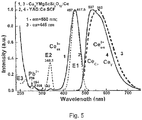
- the Fig. 5 shows a comparison of photoluminescence (PL) excitation (1, 2) and emission (3, 4) spectra of a single crystalline epitaxial film of Ca 2 YMgScSi 3 O 12 :Ce (CYMSSG:Ce) and a single crystalline Y 3 Al 5 O 12 :Ce (YAG:Ce) substrate.
- Fig. 5 combines the respective excitation spectra (1, 2) (identified also by Ce 3+ ex ) and the respective emission spectra (3, 4) (identified also by Ce 3+ em ) in one plot.
- the spectra have been normalized.
- the respective spectra are as follows:
- the excitation spectrum of CYMSSG:Ce (1) has been detected by a respective emission at 550 nm.
- the emission spectrum of CYMSSG:Ce (3) has been excited by a respective excitation at 445 nm.
- the PL measurements were performed at room temperature.
- the excitation band (1) of CYMSSG:Ce is broader than the excitation band (2) of YAG:Ce. Furthermore, it is observed that the emission band (3) of CYMSSG:Ce is broader than the emission band (4) of YAG:Ce.
- CYMSSG:Ce The reason for the broader bands of CYMSSG:Ce is the formation of Ce 3+ multicenters in CYMSSG:Ce. Accordingly, a Ceca-center is formed in the position of Ca 2+ , and a Ce Y -center is formed in the position of Y 3+ . The formation of these centers causes an elongation of the PL emission spectrum into the orange and red wavelength range.
- the denominations E1, E2, E3 correspond to the absorption bands of cerium ions in the valence state 3+.
- the denomination Pb 2+ corresponds to the absorption bands of lead ions in the valence state 2+.
- the Fig. 6 shows a comparison of photoluminescence (PL) excitation (1, 2) and emission (3,4) spectra of a composite wavelength converter formed by a single crystalline epitaxial film of Ca 2 YMgScSi 3 O 12 :Ce (CYMSSG:Ce) together with a single crystalline Y 3 Al 5 O 12 :Ce (YAG:Ce) substrate and a single crystalline Y 3 Al 5 O 12 :Ce (YAG:Ce) substrate alone.
- the Fig. 6 again, combines the respective excitation spectra and the respective emission spectra in one plot.
- the spectra have been normalized.
- the respective spectra are as follows:
- the excitation spectra (1, 2) are detected by a respective emission at 580 nm.
- the emission spectra (3, 4) are excited by a respective excitation at 450 nm. Accordingly, a blue LED is used for exciting (see "Blue LED”).
- the PL measurements were performed at room temperature.
- the emission band (3) of the CYMSSG:Ce + YAG:Ce composite wavelength converter is broader than the emission band (4) of the YAG:Ce substrate due to the formation of Ce 3+ multicenters in CYMSSG:Ce. Accordingly, a Ceca-center is formed in the position of Ca 2+ , and a Ce Y -center is formed in the position of Y 3+ . The formation of these centers causes an elongation of the PL emission spectrum into the orange and red wavelength range.
- the Fig. 7 shows a comparison of photoluminescence (PL) excitation (1, 2) and emission (3,4) spectra of a composite wavelength converter formed by a single crystalline epitaxial film of Ca 2 YMgScSi 3 O 12 :Ce, Mn (CYMSSG:Ce, Mn) together with a single crystalline Y 3 Al 5 O 12 :Ce (YAG:Ce) substrate and a single crystalline Y 3 Al 5 O 12 :Ce (YAG:Ce) substrate alone.
- the Fig. 7 again, combines the respective excitation spectra and the respective emission spectra in one plot.
- the spectra have been normalized.
- the respective spectra are as follows:
- the excitation spectra (1, 2) have been detected by a respective emission at 580 nm.
- the emission spectra (3, 4) have been excited by a respective excitation at 450 nm. Accordingly, a blue LED is used for exciting (see "Blue LED”).
- the PL measurements were performed at room temperature.
- Fig. 7 differs from the comparison of Fig. 6 in that the epitaxial film of composite wavelength converter is co-doped with Mn 2+ ions.
- the single crystalline epitaxial film of Ca 2 YMgScSi 3 O 12 :Ce, Mn (CYMSSG:Ce, Mn) provides a second activator.
- the emission band (3) of the CYMSSG:Ce, Mn + YAG:Ce composite wavelength converter is broader than the emission band (4) of the YAG:Ce substrate due to the formation of Ce 3+ multicenters in CYMSSG:Ce. Accordingly, a Ceca-center is formed in the position of Ca 2+ , and a Ce Y -center is formed in the position of Y 3+ . The formation of these centers causes an elongation of the emission spectrum into the orange and red wavelength range.
- an effective energy transfer from the Ce 3+ ions to the Mn 2+ ions causes a further elongation of the emission spectrum (3) of the CYMSSG:Ce, Mn + YAG:Ce composite wavelength converter into the orange and partly red wavelength range.
- Ce 3+ doped and Eu 3+ , Pr 3+ , Tb 3+ and Mn 2+ co-doped Ca 2 YMgScSi 3 O 12 and Ca 3 Sc 2 Si 3 O 12 SCFs are grown using the LPE method onto Ce 3+ doped YAG:Ce or LuAG:Ce and GAGG:Ce substrates, respectively.
- the substrate emits mainly in the yellow range, and the Ce 3+ doped and rare-earth or transition metal doped Ca 2 YMgScSi 3 O 12 and Ca 3 Sc 2 Si 3 O 12 epitaxial films emit in the orange-red ranges. Accordingly, a high-power white LED can be realized.
- the CRI coordinates and the color temperature resulting by the inventive composite wavelength converter and/or the CRI coordinates and the color temperature of the inventive WLED can be easily tuned.
- a 464 nm LED emitting light in the blue wavelength range (see “Diode” in Fig. 8A ) has been used for the excitation of the respective converters.
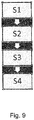
- the Fig. 9 shows a flow diagram illustrating the inventive method of preparation of a composite wavelength converter for an LED.
- a substrate 10 is provided.
- the substrate is Y 3 Al 5 O 12 :Ce garnet (YAG:Ce), Lu 3 Al 2 Ga 3 O 12 :Ce garnet (LuAG:Ce) or Gd 3 Al 2.5 Ga 2.5 O 12 :Ce garnet (GAGG:Ce) with Ce 3+ ions being the first activator.
- the Ce 3+ ions are provided as the first dopant.
- the Ce 3+ ions have a concentration of for example 0.1 mole %.
- an epitaxial film 20 is deposited onto both sides of the oriented planes of the substrate 10 using the liquid phase epitaxy method. Accordingly, the substrate 10 is embedded in a melt-solution containing flux oxides and garnet crystal forming components.
- the melt-solution for example, contains PbO and B 2 O 3 as flux oxides.
- the thickness of the epitaxial film 20 on each side of the substrate 10 is for example 100 ⁇ m.
- the epitaxial film 20 is provided with Ce 3+ ions as first activator (first dopant).
- the Ce 3+ ions have a concentration of for example 0.1 mole %.
- the epitaxial film 20 is provided with a second activator selected from one of Eu 3+ , Pr 3+ , Tb 3+ and Mn 2+ ions.
- the second activator can be a second dopant or a substituent (garnet constituent).
- the second activator has a concentration for example 2 % of Eu 3+ , Pr 3+ or Tb 3+ ions per mole, or 0,7 % of Mn 2+ ions per mole.
- the epitaxial film 20 could have one of the following compositions: Tb 3 Al 5 O 12 :Ce,Eu, Tb 3 Al 5 O 12 :Ce,Pr or Tb 3 Al 5 O 12 :Ce,Mn; Ca 2 YMgScSi 3 O 12 :Ce,Mn, Ca 2 YMgScSi 3 O 12 :Ce,Eu or Ca 3 Sc 2 Si 3 O 12 :Ce,Pr.
- a first additional epitaxial film 30 is deposited directly onto the epitaxial film 20 on both sides of the substrate 10 using the liquid phase epitaxy method.
- the thickness of the first additional epitaxial film 30 on each side of the substrate is for example 100 ⁇ m.
- a second additional epitaxial film 40 can be deposited directly onto the first additional epitaxial film 30 on both sides of the substrate 10 using the liquid phase epitaxy method.
- the thickness of the second additional epitaxial film 40 on each side of the substrate 10 is for example 100 ⁇ m.
- the first additional epitaxial film 30 (and optionally the second additional epitaxial film 40) is provided with Ce 3+ ions as first activator (first dopant).
- the Ce 3+ ions have a concentration of for example 0.1 mole %.
- the first additional epitaxial film 30 is provided with a second activator selected from one of Eu 3+ , Pr 3+ , Tb 3+ and Mn 2+ ions.
- the second additional epitaxial film 40 is provided with a second activator selected from one of Eu 3+ , Pr 3+ , Tb 3+ and Mn 2+ ions.
- the second activator can be a second dopant or a substituent (garnet constituent).
- the second activator has a concentration for example 2 % of Eu 3+ , Pr 3+ or Tb 3+ ions per mole, or 0,7 % of Mn 2+ ions per mole.
- the first additional epitaxial film 30, for example, could have one of the following compositions: Tb 3 Al 5 O 12 :Ce,Eu, Tb 3 Al 5 O 12 :Ce,Pr or Tb 3 Al 5 O 12 :Ce,Mn; Ca 2 YMgScSi 3 O 12 :Ce,Mn, Ca 2 YMgScSi 3 O 12 :Ce,Eu or Ca 3 Sc 2 Si 3 O 12 :Ce,Pr.
- the second additional epitaxial film 40 could have one of the following compositions: Tb 3 Al 5 O 12 :Ce,Eu, Tb 3 Al 5 O 12 :Ce,Pr or Tb 3 Al 5 O 12 :Ce,Mn; Ca 2 YMgScSi 3 O 12 :Ce,Mn, Ca 2 YMgScSi 3 O 12 :Ce,Eu or Ca 3 Sc 2 Si 3 O 12 :Ce,Pr.
- the step S2 (and optionally S3), i.e. the deposition of the epitaxial film 20, first additional epitaxial film 30 and/or second additional epitaxial film 40, occurs at growth temperatures of about 1000°C, at an overcooling rate of the melt-solution of about 20°C, and at a growth rate of about 0.3 ⁇ m/min.
- the substrate 10 having the epitaxial film 20, first additional epitaxial film 30 and/or second additional epitaxial film 40 deposited thereon forms an epitaxial structure.
- the epitaxial structure is for example a wafer of a diameter of 3 inch.
- the epitaxy is performed in a crucible having a diameter of about 6 inch.
- the epitaxial structure is cut in a plurality of individual samples, each having identical optical properties.
- the epitaxial structure is cut in 4000 individual samples being rectangular cuboids, each having a square base plane of 2mm ⁇ 2mm.
- the cutting is for example performed by a laser device.
Landscapes
- Chemical & Material Sciences (AREA)
- Organic Chemistry (AREA)
- Materials Engineering (AREA)
- Engineering & Computer Science (AREA)
- Metallurgy (AREA)
- Crystallography & Structural Chemistry (AREA)
- Inorganic Chemistry (AREA)
- Physics & Mathematics (AREA)
- Optics & Photonics (AREA)
- General Physics & Mathematics (AREA)
- Health & Medical Sciences (AREA)
- Toxicology (AREA)
- Luminescent Compositions (AREA)
- Led Device Packages (AREA)
- Optical Filters (AREA)
Abstract
Description
- The invention refers to a composite wavelength converter for a light emitting diode (LED), to a method of preparation of a composite wavelength converter, and to a white LED light source.
- Wavelength converters are known in prior art to convert a portion of the light of a given wavelength emitted by an LED into light having a higher wavelength, such that, as a result, a spectrum of white light is emitted.
- According to the
European Patent EP 2 670 817 B1 , a wavelength converter comprising a monocrystalline substrate and a monocrystalline thin film produced thereon by pulsed laser deposition (PLD) is disclosed. As substrate, undoped yttrium aluminum garnet, i.e. Y3Al5O12 garnet (YAG), and, as thin film, cerium-activated yttrium aluminum garnet, i.e. Y3Al5O12:Ce garnet (YAG:Ce) or cerium-activated lutetium aluminum garnet, i.e. Lu3Al5O12:Ce garnet (LuAG:Ce) are proposed. By providing a lattice mismatch between the substrate and the thin film, a compressive or tensile strain is induced which is used to produce a blue-shift or a red-shift in the emission of the thin film. However, the known wavelength converter has a limited quantum efficiency. - The object of the present invention is to overcome the disadvantages of the state of the art. In particular, it is intended to provide a composite wavelength converter having a particularly good quantum yield, a method of preparation of such a composite wavelength converter, and a white LED light source comprising an LED and such a composite wavelength converter.
- The object is achieved by the features of
claim 1 regarding the composite wavelength converter, claim 9 regarding the preparation method, and claim 16 regarding the white LED light source. Expedient embodiments of the invention result from the dependent claims. - In accordance with the invention, the composite wavelength converter comprises a substrate formed by a first layer of single crystalline garnet phosphor presenting first emission and excitation spectra. The first layer of single crystalline garnet phosphor (i.e. the substrate) has a cubic crystal structure, a first lattice parameter and oriented crystal planes. The first layer of single crystalline garnet phosphor (i.e. the substrate) contains a first activator. In the context of this application, an activator is preferably a substituent (i. e. the activator is provided as a constituent of a single crystalline garnet phosphor) or a dopant. The first activator is preferably a first dopant.
- The inventive composite wavelength converter further comprises an epitaxial film formed by liquid phase epitaxy on the top and bottom of the substrate as a second layer of single crystalline garnet phosphor. The second layer of single crystalline garnet phosphor (i.e. the epitaxial film) contains the first activator and preferably at least one second activator. The first activator is preferably a first dopant and/or the second activator(s) is/are preferably (a) second dopant(s). The second layer of single crystalline garnet phosphor (i.e. the epitaxial film) presents second emission and excitation spectra and has a cubic crystal structure and a second lattice parameter. The second layer of single crystalline garnet phosphor (i.e. the epitaxial film) is arranged directly on the top and bottom of the substrate on the oriented crystalline planes of the substrate (i.e. of the first layer of single crystalline garnet phosphor).
- Liquid-phase epitaxy (LPE) is a method to grow single crystalline layers from a melt-solution on single crystalline substrates. The material to be deposited is dissolved at temperatures well below its melting point in the melt of another material. Activators (preferably as dopants) are added to the melt. The substrate is cooled. The deposition of the material on the substrate is preferably performed at conditions that are close to the equilibrium between dissolution and deposition. The deposited layer is advantageously single crystalline.
- In accordance with the invention, the second emission and excitation spectra are different from the first emission and excitation spectra. However, in particular, the excitation spectra of the substrate (i.e. the first layer of single crystalline garnet phosphor) and of the epitaxial film (i.e. second layer of single crystalline garnet phosphor) can be only slightly different.
- Furthermore, in accordance with the invention, the difference between the first lattice parameter and the second lattice parameter results in a lattice mismatch within a range of about -2.0 and +2.0 %, preferably of about -1.0 and +1.0 %. The thickness of the epitaxial film on the top and on the bottom of the substrate, respectively, is at least 2 µm, preferably at least 20 µm, more preferably at least 30 µm, most preferably at least 50 µm.
- The composite wavelength converter can be excited by the light of a given wavelength emitted by a light emitting diode (LED). In consequence, the composite wavelength converter is adapted to emit light of a higher wavelength such that, as a result, a spectrum of white light is emitted.
- Advantageously, both, the substrate and the epitaxial film are excited by the light emitted by the LED. Preferably, each of the substrate and the epitaxial film, are adapted to emit light in consequence. Preferably, the epitaxial film is adapted to emit light of a wavelength range differing from the wavelength range emitted by the substrate.
- According to a first example, blue light can be emitted by a light emitting diode (LED). In this case, the composite wavelength converter is preferably adapted to convert a portion (preferably between 40 and 80 %, more preferably about 60%) of the blue light into light of a higher wavelength, preferably green, yellow, orange and/or red light, such that, as a result of mixing the light emitted by the LED and the light converted the composite wavelength converter, a spectrum of white light is emitted. Accordingly, by providing the composite wavelength converter, a blue LED results to become a white light emitting diode (white LED or WLED). The emission spectra of the substrate and of the epitaxial film can be tuned by adapting the composition of the substrate and of the epitaxial film, in particular by adapting the selection and concentration of the activators in the substrate and in the epitaxial film. By adapting these emission spectra, the CRI coordinates and the color temperature of the WLED can be tuned.
- According to a second example, UV-light can be emitted by a light emitting diode (LED). In this case, the composite wavelength converter is adapted to convert essentially 100% of the UV-light into visible light such that, as a result, a spectrum of white light is emitted by the WLED. Accordingly, by providing the composite wavelength converter, a UV-LED results to become a WLED. Again, the emission spectra of the substrate and of the epitaxial film can be tuned by adapting the composition of the substrate and of the epitaxial film, in particular by adapting the selection and concentration of the activators in the substrate and in the epitaxial film. By adapting these emission spectra, the CRI coordinates and the color temperature of the WLED can be tuned.
- The inventive composite wavelength converter provides both, a very low lattice mismatch and a particularly thick epitaxial layer. It has been shown that the inventive composite wavelength converter provides a very good quantum efficiency. The quantum yield of the inventive composite wavelength converter is at least 80%. Accordingly, high power white light emitting diodes (white LED or WLED) can be realized based on the inventive composite wavelength converter. Furthermore, the provision of both, substrate and the epitaxial film as light conversion layers, gives good variation possibilities regarding the spectrum. Thus, by the mixing of the emissions coming from the substrate and the epitaxial film, the CRI coordinates and the color temperature resulting by the inventive composite wavelength converter can be easily tuned.
- According to an advantageous embodiment of the invention, the converter comprises one or two additional epitaxial films, namely a first and optionally a second additional epitaxial film.
- Advantageously, the first additional epitaxial film is formed by liquid phase epitaxy as a third layer of single crystalline garnet phosphor with the first activator and preferably at least with one second activator. The first activator is preferably a first dopant and/or the second activator(s) is/are preferably (a) second dopant(s). Advantageously, the third layer of single crystalline garnet phosphor (i.e. the first additional epitaxial film) is arranged directly on the epitaxial film (i.e. on the second layer of single crystalline garnet phosphor) on the top and bottom side of the substrate, presents third emission and excitation spectra, and has a cubic crystal structure and a third lattice parameter.
- The third layer of single crystalline garnet phosphor is preferably different from the second layer of single crystalline garnet phosphor. The third emission and excitation spectra are different from the first emission and excitation spectra and preferably different from the second emission and excitation spectra. However, in particular, the excitation spectra of the substrate (i.e. the first layer of single crystalline garnet phosphor) and/or of the epitaxial film (i.e. second layer of single crystalline garnet phosphor) and/or of the first additional epitaxial film (i.e. the third layer of single crystalline garnet phosphor) can be only slightly different.
- Advantageously, the difference between the third lattice parameter and the second lattice parameter results in a lattice mismatch within a range of about - 2.0 and +2.0 %, preferably of about -1.0 and +1.0 %. The thickness of the first additional epitaxial film (i.e. of the second layer of single crystalline garnet phosphor) on the top and on the bottom side of the substrate, respectively, is at least 2 µm, preferably at least 20 µm, more preferably at least 30 µm, most preferably at least 50 µm.
- Advantageously, the second additional epitaxial film is formed by liquid phase epitaxy as a fourth layer of single crystalline garnet phosphor with the first activator and preferably at least with one second activator. The first activator is preferably a first dopant and/or the second activator(s) is/are preferably (a) second dopant(s). Advantageously, the fourth layer of single crystalline garnet phosphor (i.e. the second additional epitaxial film) is arranged directly on the first additional epitaxial film (i.e. on the third layer of single crystalline garnet phosphor) on the top and bottom side of the substrate, presents fourth emission and excitation spectra, and has a cubic crystal structure and a fourth lattice parameter,
- The fourth layer of single crystalline garnet phosphor is preferably different from the second and/or third layer of single crystalline garnet phosphor. The fourth emission and excitation spectra are different from the first emission and excitation spectra and preferably different from the second and/or third emission and excitation spectra. However, in particular, the excitation spectra of the substrate (i.e. the first layer of single crystalline garnet phosphor) and/or of the epitaxial film (i.e. second layer of single crystalline garnet phosphor) and/or of the first additional epitaxial film (i.e. the third layer of single crystalline garnet phosphor) and/or of the second additional epitaxial film (i.e. the fourth layer of single crystalline garnet phosphor) can be only slightly different.
- Advantageously, the difference between the fourth lattice parameter and the third lattice parameter results in a lattice mismatch within a range of about -2.0 and +2.0 %, preferably of about -1.0 and +1.0 %. The thickness of the second additional epitaxial film on the top and on the bottom side of the substrate, respectively, is at least 2 µm, preferably at least 20 µm, more preferably at least 30 µm, most preferably at least 50 µm.
- The second activator (or second activators) of the epitaxial film, of the first additional epitaxial film and/or of the second additional epitaxial film are preferably different and/or are preferably present in a different concentration.
- Advantageously, the additional epitaxial film or the additional epitaxial films are excited by the light emitted by the LED and are cause to emit light of a wavelength range different to the wavelength range emitted by the substrate and/or epitaxial film. Thus, by the provision of one or two additional epitaxial film(s), the overall emission spectrum is improved. There are still more variation possibilities regarding the spectrum. Thus, by the mixing of the emissions coming from the substrate and the epitaxial film, the CRI coordinates and the color temperature resulting by the inventive composite wavelength converter can be easily tuned. Furthermore, very thick single crystalline epitaxial layers can be provided. It has been shown that the provision of one or two additional epitaxial film(s) enables a particularly good quantum efficiency. Accordingly, high power white light emitting diodes (white LED or WLED) can be realized based on the inventive composite wavelength converter.
- According to a further advantageous embodiment of the invention, the first activator is Ce3+ ions. The Ce3+ ions are preferably present as a first dopant. In the substrate, the Ce3+ ions preferably have a concentration from about 0.001 to about 1 mole %, more preferably from 0.05 to 0.15 mole %. In the epitaxial film, first additional epitaxial film and/or second additional epitaxial film, the Ce3+ ions preferably have a concentration from about 0.001 to about 1 mole %, more preferably from 0.05 to 0.1 mole %. Alternatively, the first activator, in particular the first dopant, could be one from Eu3+, Pr3+, Tb3+ and Mn2+ ions.
- According to a further advantageous embodiment of the invention, the second activator is one from Eu3+, Pr3+, Tb3+ and Mn2+ ions. The second activator is preferably present as second dopant. Accordingly, the second dopant is one from R = Eu3+, Pr3+, Tb3+ and Mn2+ ions. Alternatively, the second activator can be a substituent (i. e. the activator can be provided as a constituent of the respective garnet). The second activator, in particular the second dopant, preferably has a concentration from about 0.001 to about 5 % of Eu3+, Pr3+ or Tb3+ ions per mole, more preferably from 1 to 3 mole %, or from about 0.001 to about 3 % of Mn2+ ions per mole, more preferably from 0,1 to 1 mole %.
- In the epitaxial film, the first additional epitaxial film and/or the second additional epitaxial film, respectively, a different one from Eu3+, Pr3+, Tb3+ and Mn2+ ions is preferably present as second activator. Furthermore, several second activators selected, in particular several second dopants R, from Eu3+, Pr3+, Tb3+ and Mn2+ ions can be present in the epitaxial film, several second activators, in particular several second dopants R, selected from Eu3+, Pr3+, Tb3+ and Mn2+ ions can be present in the first additional epitaxial film and/or several second activators, in particular several second dopants R, selected from Eu3+, Pr3+, Tb3+ and Mn2+ ions can be present in the second additional epitaxial film.
- Advantageously, the second activator, in particular the second dopant, is or the second activators, in particular the second dopants, are selected regarding the excitation wavelength (or excitation wavelength range) provided by the light emitting diode (LED). Accordingly, in case of a blue light emitting LED, Mn2+ can be preferably selected. In case of an UV-light emitting LED, Eu3+ can be preferably selected.
- The additional provision of Tb3+ is particularly advantageous in case of providing Eu3+ and/or Mn2+. Tb3+ can be provided in the same layer as Eu3+ and/or Mn2+ or in a different layer, preferably in a neighboring layer. Tb3+ can play an important role in the indirect excitation of Eu3+ and/or Mn2+.
- Advantageously, the provision of one or more second activators, the possible selection of different ions as second activator, the possible provision of the second activator as dopant or as substituent, and/or the possible provision of several second activators in several layers still increase the variation possibilities regarding the resulting white light spectrum provided by the invention. Thus, by the mixing of the emissions coming from the substrate and the epitaxial film, the CRI coordinates and the color temperature resulting by the inventive composite wavelength converter can be easily tuned.
- According to a further advantageous embodiment of the invention, the substrate is Y3Al5O12:Ce garnet (YAG:Ce), Lu3Al5-sGasO12:Ce garnet (LuAG:Ce) or Gd3Al5-sGasO12:Ce garnet (GAGG:Ce). The composition parameter s is between 2.5 and 3. As concrete examples, the LuAG:Ce substrate is preferably Lu3Al2Ga3O12:Ce and the GAGG:Ce substrate is preferably Gd3Al2.5Ga2.5O12: Ce.
- Advantageously, the substrate being Y3Al5O12:Ce garnet (YAG:Ce) and/or being Gd3Al5-sGasO12:Ce garnet (GAGG:Ce), wherein s is between 2.5 and 3, in particular Gd3Al2.5Ga2.5O12:Ce, can be excited by a excitation wavelength of 440 - 465 nm, preferably of about 450nm. Thus, these substrates are preferably chosen in the case of an excitation by a blue light emitting LED.
- Advantageously, the substrate being Lu3Al5-sGasO12:Ce garnet (LuAG:Ce), wherein s is between 2.5 and 3, in particular Lu3Al2Ga3O12:Ce, can be excited by a the excitation wavelength, of 340 - 360 nm, preferably of about 345 nm. Thus, this substrate is preferably chosen in the case of an excitation by a UV-light emitting LED.
- According to a further advantageous embodiment of the invention, the thickness of the substrate is between 0.3 and 1 mm, preferably between 0.45 and 0.5 mm.
- According to a further advantageous embodiment of the invention, the epitaxial film, first additional epitaxial film and/or second additional epitaxial film is/are formed by a mixed garnet compound having a composition represented by a formula X = A1 3B1 2C1 3O12:Ce,R.
- The constituents of the formula X are as follows: A1 is Ca2+ ions; B1 is Sc3+ or Al3+ or Ga3+ ions, C1 is Si4+ or Ge4+ ions and R is the second dopant.
- According to an alternative advantageous embodiment of the invention, the epitaxial film, first additional epitaxial film and/or second additional epitaxial film is/are formed by a mixed garnet compound having a composition represented by a formula Y = A1 3-xA2 xB1 2-yB2 yC1 3-zC2 zO12:Ce,R.
- The constituents of the formula Y are as follows: A1 is Ca2+ ions; A2 is Y3+, Lu3+, La3+, Tb3+ and Gd3+ ions; B1 is Mg2+ ions, B2 is Sc3+ or Al3+ or Ga3+ ions, C1 is Si4+ ions, C2 is Ge4+ ions and R is the second dopant.
- The composition parameters of the formula Y are as follows: 0 < x < 1.0, 0 < y < 2, and 0 < z < 3.
- Tb3+ ions are preferably either used as substituent (constituent of the garnet) A2 or as first or second dopant. In the context of the present application, the Tb3+ ions are called "activator" in these both cases. Accordingly, the epitaxial film, first additional epitaxial film and/or second additional epitaxial can be provided with three activators, preferably with Ce3+, Tb3+ and Eu3+. As an example, the epitaxial film, first additional epitaxial film and/or second additional epitaxial can be Tb3Al5O12:Ce,Eu. The Tb3+ ions have an important role in the energy transfer from Ce3+ ions to Eu3+ ions (and also in the energy transfer from Ce3+ ions to Mn2+ ions). Therefore, providing Tb3+ ions in a Eu3+-doped film or in a Mn2+-doped film causes an improved quantum efficiency.
- According to a further advantageous embodiment of the invention, the thickness of the epitaxial film (i.e. of the second layer of single crystalline garnet phosphor) on the top and/or on the bottom side of the substrate, respectively, is at most 200 µm, preferably at most 100 µm.
- Advantageously, the thickness of the first additional epitaxial film (i.e. of the third layer of single crystalline garnet phosphor) on the top and/or on the bottom side of the substrate, respectively, is at most 200 µm, preferably at most 100 µm.
- Advantageously, the thickness of the second additional epitaxial film (i.e. of the fourth layer of single crystalline garnet phosphor) on the top and/or on the bottom side of the substrate, respectively, is at most 200 µm, preferably at most 100 µm.
- By limiting the thickness of the thickness of the epitaxial film, of the first additional epitaxial film, and/or of the second additional epitaxial film a good quality of a single crystalline film can be ensured.
- In accordance with the invention, the method of preparation of a composite wavelength converter for an LED comprises the following steps:
- providing a substrate formed by a first layer of single crystalline garnet phosphor, having a cubic crystal structure, oriented crystal planes and containing a first activator, wherein the substrate is preferably Y3Al5O12:Ce garnet (YAG:Ce), Lu3Al5-sGasO12:Ce garnet (LuAG:Ce, preferably Lu3Al2Ga3O12:Ce) or Gd3Al5-sGasO12:Ce garnet (GAGG:Ce, preferably Gd3Al2.5Ga2.5O12:Ce) with Ce3+ ions being the first activator, wherein the composition parameter s is between 2.5 and 3, and
- depositing an epitaxial film forming a second layer of single crystalline garnet phosphor with the first activator and preferably at least with one second activator onto both sides of the oriented planes of the substrate using the liquid phase epitaxy method, wherein the thickness of the epitaxial film on each side of the substrate is at least 2 µm, preferably at least 20 µm, more preferably at least 30 µm, most preferably at least 50 µm.
- In the context of this application, an activator is preferably a substituent (i.e. a constituent of a single crystalline garnet phosphor) or a dopant. The first activator is preferably a first dopant and/or the second activator(s) is/are preferably (a) second dopant(s).
- Advantageously, the features of the inventive composite wavelength converter presented above also apply to the method of preparation of a composite wavelength converter. In particular, the substrate (first layer of single crystalline garnet phosphor) presents first emission and excitation spectra and has a first lattice parameter. The epitaxial film (second layer of single crystalline garnet phosphor) presents second emission and excitation spectra and has a second lattice parameter.
- Advantageously, the second emission and excitation spectra are different from the first emission and excitation spectra. However, in particular, the excitation spectra of the substrate (i.e. the first layer of single crystalline garnet phosphor) and of the epitaxial film (i.e. second layer of single crystalline garnet phosphor) can be only slightly different.
- Advantageously, the difference between the first lattice parameter and the second lattice parameter results in a lattice mismatch within a range of about - 2.0 and +2.0 %, preferably of about -1.0 and +1.0 %.
- The inventive preparation method provides a composite wavelength converter having both, a very low lattice mismatch and a particularly thick epitaxial layer. It has been shown that, accordingly, a very good quantum efficiency is realized. Furthermore, based on the inventive preparation method, high power white light emitting diodes (white LED or WLED) can be realized.
- Advantageously, the first activator is Ce3+ ions. The Ce3+ ions are preferably used as a first dopant. In the substrate, the Ce3+ ions preferably have a concentration from about 0.001 to about 1 mole %, more preferably from 0.05 to 0.15 mole %. In the epitaxial film, first additional epitaxial film and/or second additional epitaxial film, the Ce3+ ions preferably have a concentration from about 0.001 to about 1 mole %, more preferably from 0.05 to 0.1 mole %. Alternatively, the first activator, in particular the first dopant, could be one from Eu3+, Pr3+, Tb3+ and Mn2+ ions.
- According to an advantageous embodiment of the invention, the method of preparation comprises the additional step of depositing a first additional epitaxial film forming a third layer of single crystalline garnet phosphor with the first activator and preferably at least with one second activator (preferably directly) onto the epitaxial film (i.e. the second layer of single crystalline garnet phosphor) on both sides of the substrate using the liquid phase epitaxy method, wherein the thickness of the first additional epitaxial film (i.e. the third layer of single crystalline garnet phosphor) on each side of the substrate is at least 2 µm, preferably at least 20 µm, more preferably at least 30 µm, most preferably at least 50 µm.
- Furthermore, the method of preparation optionally comprises the additional step of depositing a second additional epitaxial film forming a fourth layer of single crystalline garnet phosphor with the first activator and preferably at least with one second activator (preferably directly) onto the first additional epitaxial film (i.e. the third layer of single crystalline garnet phosphor) on both sides of the substrate using the liquid phase epitaxy method, wherein the thickness of the second additional epitaxial film (i.e. the fourth layer of single crystalline garnet phosphor) on each side of the substrate is at least 2 µm, preferably at least 20 µm, more preferably at least 30 µm, most preferably at least 50 µm.
- The first activator is preferably a first dopant and/or the second activator(s) is/are preferably (a) second dopant(s).
- Advantageously, the third layer of single crystalline garnet phosphor (i.e. the first additional epitaxial film) presents third emission and excitation spectra, and has a cubic crystal structure and a third lattice parameter.
- The third layer of single crystalline garnet phosphor is preferably different from the second layer of single crystalline garnet phosphor. The third emission and excitation spectra are different from the first emission and excitation spectra and preferably different from the second emission and excitation spectra. However, in particular, the excitation spectra of the substrate (i.e. the first layer of single crystalline garnet phosphor) and/or of the epitaxial film (i.e. second layer of single crystalline garnet phosphor) and/or of the first additional epitaxial film (i.e. the third layer of single crystalline garnet phosphor) can be only slightly different.
- Advantageously, the difference between the third lattice parameter and the second lattice parameter results in a lattice mismatch within a range of about - 2.0 and +2.0 %, preferably of about -1.0 and +1.0 %.
- Advantageously, the fourth layer of single crystalline garnet phosphor (i.e. the second additional epitaxial film) presents fourth emission and excitation spectra, and has a cubic crystal structure and a fourth lattice parameter.
- The fourth layer of single crystalline garnet phosphor is preferably different from the second and/or third layer of single crystalline garnet phosphor. The fourth emission and excitation spectra are different from the first emission and excitation spectra and preferably different from the second and/or third emission and excitation spectra. However, in particular, the excitation spectra of the substrate (i.e. the first layer of single crystalline garnet phosphor) and/or of the epitaxial film (i.e. second layer of single crystalline garnet phosphor) and/or of the first additional epitaxial film (i.e. the third layer of single crystalline garnet phosphor) and/or of the second additional epitaxial film (i.e. the fourth layer of single crystalline garnet phosphor) can be only slightly different.
- Advantageously, the difference between the fourth lattice parameter and the third lattice parameter results in a lattice mismatch within a range of about -2.0 and +2.0 %, preferably of about -1.0 and +1.0 %.
- The second activator (or second activators) of the epitaxial film, of the first additional epitaxial film and/or of the second additional epitaxial film are preferably different and/or are preferably used in a different concentration.
- By the provision of one or two additional epitaxial film(s), the overall emission spectrum is improved. There are still more variation possibilities regarding the spectrum. Thus, by the mixing of the emissions coming from the substrate and the epitaxial film, the CRI coordinates and the color temperature resulting by the inventive composite wavelength converter can be easily tuned. Furthermore, very thick single crystalline epitaxial layers can be provided. It has been shown that, by providing one or two additional epitaxial film(s), a particularly good quantum efficiency can be realized. Thus, based on the inventive preparation method, high power white light emitting diodes (white LED or WLED) can be realized.
- According to a further advantageous embodiment of the invention, in the method of preparation, the substrate is embedded in a melt-solution containing flux oxides and garnet crystal forming components. The melt-solution preferably contains PbO and B2O3 as flux oxides or Bi2O3 and B2O3 as flux oxides.
- The melt-solution preferably contains the garnet crystal forming components for producing the epitaxial film, first additional epitaxial film and/or second additional epitaxial film formed by a mixed garnet compound having a composition represented by a formula
X = A1 3B1 2C1 3O12:Ce,R.
- The constituents of the formula X are as follows: A1 is Ca2+ ions; B1 is Sc3+ or Al3+ or Ga3+ ions, C1 is Si4+ or Ge4+ ions and R is the second dopant.
- Alternatively, the melt-solution can contain the garnet crystal forming components for producing the epitaxial film, first additional epitaxial film and/or second additional epitaxial film formed by a mixed garnet compound having a composition represented by a formula
Y = A1 3-xA2 xB1 2-yB2 yC1 3-zC2 zO12:Ce,R.
- The constituents of the formula Y are as follows: A1 is Ca2+ ions; A2 is Y3+, Lu3+, La3+, Gd3+ and/or Tb3+ ions; B1 is Mg2+ ions, B2 is Sc3+ or Al3+ or Ga3+ ions, C1 is Si4+ ions, C2 is Ge4+ ions and R is the second dopant.
- The composition parameters of the formula Y are as follows: 0 < x < 1.0, 0 < y < 2, and 0 < z < 3.
- Advantageously, the second activator is one from Eu3+, Pr3+, Tb3+ and Mn2+ ions. The second activator is preferably used as second dopant. Accordingly, the second dopant is one from R = Eu3+, Pr3+, Tb3+ and Mn2+ ions. The second activator, however, also can be provided in the garnet as a substituent, e.g. as A2 being Tb3+ ions.
- The second activator, in particular the second dopant R, preferably has a concentration from about 0.001 to about 5 % of Eu3+, Pr3+ or Tb3+ ions per mole, more preferably from 1 to 3 mole %, or from about 0.001 to about 3 % of Mn2+ ions per mole, more preferably from 0,1 to 1 mole %.
- Advantageously, in the epitaxial film, the first additional epitaxial film and/or the second additional epitaxial film, respectively, a different one from R = Eu3+, Pr3+, Tb3+ and Mn2+ ions is preferably used as second dopant. Furthermore, several second activators, in particular several second dopants R, selected from Eu3+, Pr3+, Tb3+ and Mn2+ ions can be used in the epitaxial film, several second activators, in particular several second dopants R, selected from Eu3+, Pr3+, Tb3+ and Mn2+ ions can be used in the first additional epitaxial film and/or several second activators, in particular several second dopants R, selected from Eu3+, Pr3+, Tb3+ and Mn2+ ions can be used in the second additional epitaxial film.
- According to a further advantageous embodiment of the invention, in the method of preparation, for producing the epitaxial film, first additional epitaxial film and/or second additional epitaxial film formed by the mixed garnet compound having a composition represented by a formula X, the melt-solution contains PbO, B2O3 as flux oxides or Bi2O3 and B2O3 as flux oxides; AO, B1 2O3, C1O2, CeO2 and one of R2O3 or R4O7 or RO2 oxides as garnet crystal forming components, wherein R2O3 is preferably Eu2O3, R4O7 is preferably Pr4O7 and/or Tb4O7, and RO2 is preferably MnO2,
chosen in the respective concentrations of 90 mole % of PbO or Bi2O3, 7.5 mole % of B2O3; 0.85 mole % of AO, 0.56 mole % of B1 2O3, 0.835 mole % of C1O2, 0.015 mole % of CeO2 and 0.24 mole % of R2O3 or R4O7 or RO2 oxides. There can be a variation in the ratio between the flux oxides and the garnet crystal forming components of ±10%, preferably ±5%. Alternatively or additionally, there can be a variation in each of the garnet crystal forming components of ±10%, preferably ±5%. - Advantageously, Y3Al5O12:Ce garnet (YAG:Ce) or Lu3Al5-sGasO12:Ce garnet (LuAG:Ce) is used as substrate. The composition parameter s is between 2.5 and 3. As an example, preferably Lu3Al2Ga3O12:Ce is used as substrate.
- According to an alternative advantageous embodiment of the invention, in the method of preparation, for producing the epitaxial film, first additional epitaxial film and/or second additional epitaxial film formed by the mixed garnet compound having a composition represented by the formula Y, the melt-solution contains PbO, B2O3 as flux oxides or Bi2O3 and B2O3 as flux oxides; A1O, A2 2O3, B1O, B2 2O3; C1O2, CeO2 and one of R2O3 or R4O7 or RO2 oxides as garnet crystal forming components, wherein R2O3 is preferably Eu2O3, R4O7 is preferably Pr4O7 and/or Tb4O7, and RO2 is preferably MnO2,
chosen in respective concentrations of 90 mole % of PbO or Bi2O3, 7.5 mole % of B2O3; 0.57 mole % of A1O, 0.28 mole % of A2 2O3, 0.29 mole % of B1O, 0.27 mole % of B2 2O3; 0.835 mole % of C1O2, 0.015 mole % of CeO2 and 0.24 mole % of R2O3 or R4O7 or RO2 oxides. There can be a variation in the ratio between the flux oxides and the garnet crystal forming components of ±10%, preferably ±5%. Alternatively or additionally, there can be a variation in each of the garnet crystal forming components of ±10%, preferably ±5%. - Advantageously, the substrate is Gd3Al5-sGasO12:Ce garnet (GAGG:Ce). The composition parameter s is between 2.5 and 3.
- According to a further advantageous embodiment of the invention, in the method of preparation, the deposition of the epitaxial film, first additional epitaxial film and/or second additional epitaxial film occurs at growth temperatures in the range of 850 - 1100°C, preferably at growth temperatures in the range of 950 - 1050°C.
- Advantageously, the deposition of the epitaxial film, first additional epitaxial film and/or second additional epitaxial film occurs at an overcooling rate of the melt-solution in the range of 1 to 90°C, preferably in the range of 10 to 30°C. The overcooling rate is the difference between the temperature of saturation of melt-solution and temperature of growth.
- According to a further advantageous embodiment of the invention, in the method of preparation, the deposition of the epitaxial film, first additional epitaxial film and/or second additional epitaxial film occurs at a growth rate in the range of 0.01 to 3 µm/min, preferably in the range of 0.1 to 0.5 µm/min.
- According to a further advantageous embodiment of the invention, the substrate having the epitaxial film, first additional epitaxial film and/or second additional epitaxial film deposited thereon forms an epitaxial structure. The epitaxial structure is preferably a wafer. The wafer has preferably a diameter of 2 - 5 inch, most preferably of 3 inch. The epitaxy is preferably performed in a crucible having about the double size of the wafers. Accordingly, the crucible has preferably a diameter of about 4 - 10 inch, most preferably of about 6 inch.
- Advantageously, the method comprises the additional step of cutting the epitaxial structure in a plurality of individual samples, each having identical optical properties. Preferably, the epitaxial structure is cut in 1000 to 10000 individual samples, more preferably in 2000 to 5000 individual samples. The individual samples are preferably rectangular cuboids, each having a square base plane of 2mm ∗ 2mm, preferably of 1mm ∗ 1mm. The cutting is preferably performed by a laser device.
- In accordance with the invention, the white LED (WLED) light source comprises an LED and an inventive composite wavelength converter mounted on a light emitting surface of the LED. The composite wavelength converter converts at least a portion of light having a wavelength lying within a first range emitted by the LED into light having a wavelength lying in a second range. The wavelength lying within the second range is higher than the wavelength lying within the first range.
- The LED preferably is adapted to emit a spectral distribution in the UV- and/or visible wavelength range. The first range is preferably a portion of the spectral distribution of the LED or the whole spectral distribution of the LED. The composite wavelength converter is adapted to be excited by absorbing a photon of a wavelength lying within the first range. The accordingly excited composite wavelength converter is adapted to emit a photon of a wavelength lying within the second range, wherein the wavelength lying within the second range is higher than the wavelength lying within the first range. Preferably, the composite wavelength converter is adapted to convert (at least a portion of) a first spectral distribution emitted by the LED into a second spectral distribution, wherein an average wavelength of the second spectral distribution is higher than an average wavelength of the first spectral distribution.
- In particular, the LED can be adapted to emit blue light and/or radiation in the UV wavelength range (UV-light). Accordingly, the first range can belong to the blue wavelength range or to the UV wavelength range. Alternatively, the first range can include the blue wavelength range and/or the UV wavelength range.
- Accordingly, it is possible to realize a white LED light source without providing a blue light emitting LED.
- The second range preferably belongs to the visible wavelength range. The second range preferably includes the violet wavelength range, and/or blue wavelength range, and/or green wavelength range, and/or yellow wavelength range, and/or orange wavelength range, and/or red wavelength range. In particular, the second range can belong to the green wavelength range, and/or yellow wavelength range, and/or orange wavelength range, and/or red wavelength range.
- Advantageously, the inventive white LED provides a very good quantum efficiency. Accordingly, the inventive white LED can be realized as a high-power device. Furthermore, the provision of both, substrate and the epitaxial film as light conversion layers, gives good variation possibilities regarding the spectrum. By the mixing of the emissions coming from the substrate and the epitaxial film, the CRI coordinates and the color temperature of the inventive WLED can be easily tuned.
- According to a further advantageous embodiment of the invention, the wavelength lying within the first range belongs to the blue wavelength range. In this case, the composite wavelength converter is adapted to convert an appropriate portion of the light having the wavelength lying within the first range into light having the wavelength lying within the second range for creating a white light spectrum comprising the remaining portion of the light having the wavelength lying within the first range and the portion converted into light having the wavelength lying within the second range.
- Preferably, the composite wavelength converter is adapted to convert between 40 and 80 %, preferably about 60%, of the light having the wavelength lying within the first range into light having the wavelength lying within the second range. Accordingly, the wavelength lying within the first range, i.e. the excitation wavelength, is preferably 440 - 465 nm, more preferably about 450nm. Preferably, Y3Al5O12:Ce garnet (YAG:Ce) and/or Gd3Al5-sGasO12:Ce garnet (GAGG:Ce), wherein s is between 2.5 and 3, are chosen as substrate to be excited by this wavelength or this wavelength range, respectively.
- According to an alternative advantageous embodiment of the invention, the wavelength lying within the first range belongs to the UV wavelength range, wherein the wavelength lying within the second range belongs to the visible wavelength range. In this case, the composite wavelength converter is adapted to convert essentially 100 % of the light having the wavelength lying within the first range into light having the wavelength lying within the second range.
- Accordingly, the wavelength lying within the first range, i.e. the excitation wavelength, is preferably 340 - 360 nm, more preferably about 345 nm. Preferably, Lu3Al5-sGasO12:Ce garnet (LuAG:Ce), wherein s is between 2.5 and 3, more preferably Lu3Al2Ga3O12:Ce, is chosen as substrate to be excited by this wavelength or this wavelength range, respectively.
- The invention is now explained in more detail with reference to embodiment examples. There are shown in
- Fig. 1
- a schematic structure of a white LED light source,
- Fig. 2
- examples of a schematic structure of the composite wavelength converter,
- Fig. 3A
- XRD pattern of an example of an CSSG:Ce epitaxial film grown onto a GAGG:Ce substrate,
- Fig. 3B
- XRD pattern of an example of a CYMSSG:Ce epitaxial film grown onto a YAG:Ce substrate forming an inventive composite wavelength converter,
- Fig. 4A
- excitation spectra of Ce3+ luminescence in three different substrates,
- Fig. 4B
- emission spectra of Ce3+ luminescence in the same three different substrates,
- Fig. 5
- a comparison of excitation (1, 2) and emission (3, 4) photoluminescence spectra of CYMSSG:Ce epitaxial film (1, 3) with YAG:Ce epitaxial film (2, 4),
- Fig. 6
- a comparison of excitation (1, 2) and emission (3, 4) photoluminescence spectra of a composite wavelength converter formed by a of CYMSSG:Ce epitaxial film together with a YAG:Ce substrate (1, 3) in comparison with a YAG:Ce substrate alone (2, 4),
- Fig. 7
- a comparison of excitation (1, 2) and emission (3, 4) photoluminescence spectra of a composite wavelength converter formed by a Mn2+ co-doped CYMSSG:Ce epitaxial film together with a YAG:Ce substrate (1, 3) in comparison with a YAG:Ce substrate alone (2, 4),
- Fig. 8A
- chromaticity color coordinates of a YAG:Ce substrate alone, of a composite wavelength converter formed by a of CYMSSG:Ce epitaxial film grown on a YAG:Ce substrate (A), and of a composite wavelength converter formed by a Mn2+ co-doped CYMSSG:Ce epitaxial film grown on a YAG:Ce substrate (B),
- Fig. 8B
- color temperatures of a YAG:Ce substrate alone, of a composite wavelength converter formed by a of CYMSSG:Ce epitaxial film grown on a YAG:Ce substrate (A), and of a composite wavelength converter formed by a Mn2+ co-doped CYMSSG:Ce epitaxial film grown on a YAG:Ce substrate (B), and
- Fig. 9
- a flow diagram illustrating the inventive method.
- The
Fig. 1 shows a schematic structure of a white light emitting diode (white LED or WLED) light source. Acomposite wavelength converter 1 is mounted on a light emitting diode (LED) 100. TheLED 100 comprises acarrier 101 formed by sapphire (Al2O3). Thecarrier 101 is adapted to mount thecomposite wavelength converter 1 on the further layers of theLED 100. TheLED 100 further comprises a n-dopedlayer 102 of GaN, anactive layer 103 of (AlGaln)N, a p-dopedlayer 104 of GaN, an adhesive andmirror layer 105, and anelectroplating metal layer 106. Furthermore, the LED is provided with anohmic contact 107. - The
active layer 103 preferably emits blue light. In this case, thecomposite wavelength converter 1 is adapted to convert a portion (preferably about 60%) of the blue light into green, yellow, orange and red light such that, as a result of mixing the light emitted by theLED 100 and the light converted thecomposite wavelength converter 1, a spectrum of white light is emitted by the WLED. - Alternatively, the
active layer 103 emits UV-light. In this case, thecomposite wavelength converter 1 is adapted to convert essentially 100% of the UV-light into visible light such that, as a result, a spectrum of white light is emitted by the WLED. - The
Fig. 2 shows examples of a schematic structure of thecomposite wavelength converter 1. The inventivecomposite wavelength converters 1 are produced by liquid-phase epitaxy (LPE) by depositing one or more layers of single crystalline garnet phosphor onto asubstrate 1 formed by a first layer of single crystalline garnet phosphor. - The
Fig. 2A shows the schematic structure of acomposite wavelength converter 1 having three layers. Thesubstrate 10 is situated in the center of the three layers. Thesubstrate 10 is enclosed by an epitaxial film 20 (second layer of single crystalline garnet phosphor) at its top side and at its bottom side. Due to the preparation by LPE, theepitaxial film 20 is identical at the top side and at the bottom side of thesubstrate 10. -
Ca3Sc2Si3O12:Ce, R epitaxial film 20 Gd3Al2.5Ga2.5O12:Ce (GAGG:Ce) substrate 10Ca3Sc2Si3O12:Ce, R epitaxial film 20
lattice parameter of the substrate a = 12.228 Å -
Ca2YMgScSi3O12:Ce, R (CYMSSG:Ce, R) epitaxial film 20 Y3Al5O12:Ce (YAG:Ce) substrate 10Ca2YMgScSi3O12:Ce, R (CYMSSG:Ce, R) epitaxial film 20
lattice parameter of the substrate a=12.0005 Å -
Ca2YMgScSi3O12:Ce, R (CYMSSG:Ce, R) epitaxial film 20Lu3Al2Ga3O12:Ce (LuAG:Ce) substrate 10Ca2YMgScSi3O12:Ce, R (CYMSSG:Ce, R) epitaxial film 20
lattice parameter of the substrate a=12.088 Å - The
Fig. 2B shows the schematic structure of acomposite wavelength converter 1 having five layers. Again, thesubstrate 10 is situated in the center. Thesubstrate 10 is enclosed by theepitaxial film 20 at its top side and at its bottom side. Onto theepitaxial film 20, a first additional epitaxial film 30 (third layer of single crystalline garnet phosphor) is deposited, both, at the top side and at the bottom side of thesubstrate 10. Due to the preparation by liquid-phase epitaxy (LPE), the firstadditional epitaxial film 30, as well, is identical at the top side and at the bottom side of thesubstrate 10. -
Ca2YMgScSi3O12:Ce first additional epitaxial film 30Tb3Al5O12:Ce epitaxial film 20 Y3Al5O12:Ce (YAG:Ce) substrate 10Tb3Al5O12: Ce epitaxial film 20 Ca2YMgScSi3O12:Ce first additional epitaxial film 30 - In this example, the
epitaxial film 20 at the top side of thesubstrate 10 and at the bottom side of thesubstrate 10 can alternatively be Tb3Al5O12:Ce, R, wherein R = Eu3+, Pr3+ or Mn2+. -
Tb3Al5O12:Ce first additional epitaxial film 30Ca2YMgScSi3O12:Ce (CYMSSG:Ce) epitaxial film 20 Y3Al5O12:Ce (YAG:Ce) substrate 10Ca2YMgScSi3O12:Ce (CYMSSG:Ce) epitaxial film 20Tb3Al5O12:Ce first additional epitaxial film 30 - In this example, the first
additional epitaxial film 30 at both sides can alternatively be Tb3Al5O12:Ce, R, wherein R = Eu3+, Pr3+ or Mn2+. -
Tb2GdGa2Al3O12: Ce first additional epitaxial film 30Ca2YMgScSi3O12:Ce (CYMSSG:Ce) epitaxial film 20 Y3Al5O12:Ce (YAG:Ce) substrate 10Ca2YMgScSi3O12:Ce (CYMSSG:Ce) epitaxial film 20Tb2GdGa2Al3O12:Ce first additional epitaxial film 30 - In this example, the first
additional epitaxial film 30 at both sides can alternatively be Tb2GdGa2Al3O12:Ce, R, wherein R = Eu3+, Pr3+ or Mn2+. - The
Fig. 2C shows the schematic structure of acomposite wavelength converter 1 having seven layers. The structure ofsubstrate 10,epitaxial film 20 and firstadditional epitaxial film 30 corresponds to the structure shown inFig. 2B . This structure is enclosed by a second additional epitaxial film 40 (fourth layer of single crystalline garnet phosphor) at its top side and at its bottom side. Due to the preparation by liquid-phase epitaxy (LPE), the secondadditional epitaxial film 40, as well, is identical at the top side and at the bottom side of thesubstrate 10. - The WLED of
Fig. 1 is shown comprising acomposite wavelength converter 1 having three layers according to theFig. 2A . The inventive WLED, of course, can comprise any inventivecomposite wavelength converter 1 according to any one of thefigures 2A, 2B or 2C . - The
Fig. 3A and 3B show XRD patterns of a first and second example of an epitaxial film grown onto a substrate forming an inventive composite wavelength converter. The XRD patterns show pronounced peaks, the so-called characteristic lines. Each characteristic line is denominated according to the so-called Siegbahn notation. Accordingly, K-alpha 1 (Kα1) indicates the characteristic line of an electron transition from the highest 2p orbital of the L-shell to the innermost K-shell. K-alpha 2 (Kα2) indicates the characteristic line of an electron transition from the second 2p orbital of the L-shell to the innermost K-shell. - In the first example (
Fig. 3A ), a single crystalline film of Ca3Sc2Si3O12:Ce (CSSG:Ce) withthickness 10 µm was grown as an epitaxial film by LPE from a PbO based flux onto a single crystalline Gd3Al2,5Ga2,5O12:Ce (GAGG:Ce) garnet substrate (Example 1 fromFig. 2A ). The XRD pattern of the first example refers to the (1200) plane. The lattice parameter of the epitaxial film results as a = 12.2586 Å, the lattice parameter of the substrate results as a = 12.228 Å. Accordingly, the lattice mismatch Δa/a accounts to 0,25 %. - In the second example (
Fig. 3B ), a single crystalline film of Ca2YMgScSi3O12:Ce (CYMSSG:Ce) was grown as an epitaxial film by LPE from a PbO based flux onto a single crystalline Y3Al5O12:Ce (YAG:Ce) substrate (Example 2 fromFig. 2A ). The XRD pattern of the second example refers to the (1042) plane. The lattice parameter of the epitaxial film results as a = 12,1639 Å, the lattice parameter of the substrate results as a = 12,0054 Å. Accordingly, the lattice mismatch Δa/a accounts to 1,32 %. - The
Fig. 4A and 4B show excitation (Fig. 4A ) and emission (Fig. 4B ) spectra of the Ce3+ luminescence in three different substrates, namely: - (1): Y3Al5O12:Ce substrate (YAG:Ce),
- (2): Lu3Al2Ga3O12:Ce substrate (LuAG:Ce) and
- (3): Gd3Al2,5Ga2,5O12:Ce substrate (GAGG:Ce).
- According to the excitation spectra (
Fig. 4A ), each of the YAG:Ce substrate (1) and the GAGG:Ce substrate (3) show a peak in the range of an excitation wavelength of about 440 - 465 nm which corresponds to the wavelength range of a blue light emitting LED. The LuAG:Ce substrate (2) shows a peak in the range of an excitation wavelength of about 340 - 360 nm which corresponds to the wavelength range of a UV-light emitting LED. - According to the emission spectra (
Fig. 4B ), the YAG:Ce substrate (1) shows an emission peak of 535 nm (yellowish-green) with a broad shoulder to the yellow and orange wavelength range, the LuAG:Ce substrate (2) shows an emission peak of 483 nm (greenish-blue), and the GAGG:Ce substrate (3) shows a broad emission peak at 563 nm (yellow-green) which extends to the yellow and orange wavelength range. - The
Fig. 5 shows a comparison of photoluminescence (PL) excitation (1, 2) and emission (3, 4) spectra of a single crystalline epitaxial film of Ca2YMgScSi3O12:Ce (CYMSSG:Ce) and a single crystalline Y3Al5O12:Ce (YAG:Ce) substrate.Fig. 5 combines the respective excitation spectra (1, 2) (identified also by Ce3+ ex) and the respective emission spectra (3, 4) (identified also by Ce3+ em) in one plot. The spectra have been normalized. The respective spectra are as follows: - (1) excitation spectrum of CYMSSG:Ce,
- (2) excitation spectrum of YAG:Ce,
- (3) emission spectrum of CYMSSG:Ce,
- (4) emission spectrum of YAG:Ce.
- The excitation spectrum of CYMSSG:Ce (1) has been detected by a respective emission at 550 nm. The emission spectrum of CYMSSG:Ce (3) has been excited by a respective excitation at 445 nm. The PL measurements were performed at room temperature.
- It is observed that the excitation band (1) of CYMSSG:Ce is broader than the excitation band (2) of YAG:Ce. Furthermore, it is observed that the emission band (3) of CYMSSG:Ce is broader than the emission band (4) of YAG:Ce.
- The reason for the broader bands of CYMSSG:Ce is the formation of Ce3+ multicenters in CYMSSG:Ce. Accordingly, a Ceca-center is formed in the position of Ca2+, and a CeY-center is formed in the position of Y3+. The formation of these centers causes an elongation of the PL emission spectrum into the orange and red wavelength range.
- Furthermore, in the
Fig. 5 , the denominations E1, E2, E3 correspond to the absorption bands of cerium ions in thevalence state 3+. The denomination Pb2+ corresponds to the absorption bands of lead ions in thevalence state 2+. - The
Fig. 6 shows a comparison of photoluminescence (PL) excitation (1, 2) and emission (3,4) spectra of a composite wavelength converter formed by a single crystalline epitaxial film of Ca2YMgScSi3O12:Ce (CYMSSG:Ce) together with a single crystalline Y3Al5O12:Ce (YAG:Ce) substrate and a single crystalline Y3Al5O12:Ce (YAG:Ce) substrate alone. TheFig. 6 , again, combines the respective excitation spectra and the respective emission spectra in one plot. The spectra have been normalized. The respective spectra are as follows: - (1) excitation spectrum of the CYMSSG:Ce + YAG:Ce composite wavelength converter,
- (2) excitation spectrum of the YAG:Ce substrate alone,
- (3) emission spectrum of the CYMSSG:Ce + YAG:Ce composite wavelength converter,
- (4) emission spectrum of the YAG:Ce substrate alone.
- The excitation spectra (1, 2) are detected by a respective emission at 580 nm. The emission spectra (3, 4) are excited by a respective excitation at 450 nm. Accordingly, a blue LED is used for exciting (see "Blue LED"). The PL measurements were performed at room temperature.
- Again, the emission band (3) of the CYMSSG:Ce + YAG:Ce composite wavelength converter is broader than the emission band (4) of the YAG:Ce substrate due to the formation of Ce3+ multicenters in CYMSSG:Ce. Accordingly, a Ceca-center is formed in the position of Ca2+, and a CeY-center is formed in the position of Y3+. The formation of these centers causes an elongation of the PL emission spectrum into the orange and red wavelength range.
- The
Fig. 7 shows a comparison of photoluminescence (PL) excitation (1, 2) and emission (3,4) spectra of a composite wavelength converter formed by a single crystalline epitaxial film of Ca2YMgScSi3O12:Ce, Mn (CYMSSG:Ce, Mn) together with a single crystalline Y3Al5O12:Ce (YAG:Ce) substrate and a single crystalline Y3Al5O12:Ce (YAG:Ce) substrate alone. TheFig. 7 , again, combines the respective excitation spectra and the respective emission spectra in one plot. The spectra have been normalized. The respective spectra are as follows: - (1) excitation spectrum of the CYMSSG:Ce, Mn + YAG:Ce composite wavelength converter,
- (2) excitation spectrum of the YAG:Ce substrate alone,
- (3) emission spectrum of the CYMSSG:Ce, Mn + YAG:Ce composite wavelength converter,
- (4) emission spectrum of the YAG:Ce substrate alone.
- The excitation spectra (1, 2) have been detected by a respective emission at 580 nm. The emission spectra (3, 4) have been excited by a respective excitation at 450 nm. Accordingly, a blue LED is used for exciting (see "Blue LED"). The PL measurements were performed at room temperature.
- The comparison of
Fig. 7 differs from the comparison ofFig. 6 in that the epitaxial film of composite wavelength converter is co-doped with Mn2+ ions. Thus, inFig. 7 , the single crystalline epitaxial film of Ca2YMgScSi3O12:Ce, Mn (CYMSSG:Ce, Mn) provides a second activator. - Again, the emission band (3) of the CYMSSG:Ce, Mn + YAG:Ce composite wavelength converter is broader than the emission band (4) of the YAG:Ce substrate due to the formation of Ce3+ multicenters in CYMSSG:Ce. Accordingly, a Ceca-center is formed in the position of Ca2+, and a CeY-center is formed in the position of Y3+. The formation of these centers causes an elongation of the emission spectrum into the orange and red wavelength range.
- Furthermore, an effective energy transfer from the Ce3+ ions to the Mn2+ ions causes a further elongation of the emission spectrum (3) of the CYMSSG:Ce, Mn + YAG:Ce composite wavelength converter into the orange and partly red wavelength range.
- Thus, advantageously, Ce3+ doped and Eu3+, Pr3+, Tb3+ and Mn2+ co-doped Ca2YMgScSi3O12 and Ca3Sc2Si3O12 SCFs are grown using the LPE method onto Ce3+ doped YAG:Ce or LuAG:Ce and GAGG:Ce substrates, respectively.
- Advantageously, the substrate emits mainly in the yellow range, and the Ce3+ doped and rare-earth or transition metal doped Ca2YMgScSi3O12 and Ca3Sc2Si3O12 epitaxial films emit in the orange-red ranges. Accordingly, a high-power white LED can be realized.
- By the mixing of the emissions coming from the substrate and the epitaxial film, the CRI coordinates and the color temperature resulting by the inventive composite wavelength converter and/or the CRI coordinates and the color temperature of the inventive WLED can be easily tuned.
- The
Fig. 8A and 8B show chromaticity color coordinates (Fig. 8A ) and color temperatures (Fig. 8B ) of the following converters:
YAG:Ce: light converting substrate with thickness h=550 µm; - A: single crystalline epitaxial film of Ca2YMgScSi3O12:Ce (CYMSSG:Ce) with thickness h = 15 µm grown onto both side of YAG:Ce light converting substrate with thickness h = 550 µm and
- B: single crystalline epitaxial film of Ca2YMgScSi3O12:Ce,Mn (CYMSSG:Ce,Mn) with thickness of h = 52 µm grown onto both side of YAG:Ce light converting substrate with thickness h = 550 µm.
- A 464 nm LED emitting light in the blue wavelength range (see "Diode" in
Fig. 8A ) has been used for the excitation of the respective converters. - It is observed from the
Fig. 8 that in the succession YAG:Ce - A - B, an increasingly warmer white impression is realized. - The
Fig. 9 shows a flow diagram illustrating the inventive method of preparation of a composite wavelength converter for an LED. - In a first step S1, a
substrate 10 is provided. For example, the substrate is Y3Al5O12:Ce garnet (YAG:Ce), Lu3Al2Ga3O12:Ce garnet (LuAG:Ce) or Gd3Al2.5Ga2.5O12:Ce garnet (GAGG:Ce) with Ce3+ ions being the first activator. In particular, the Ce3+ ions are provided as the first dopant. The Ce3+ ions have a concentration of for example 0.1 mole %. - In a step S2, an
epitaxial film 20 is deposited onto both sides of the oriented planes of thesubstrate 10 using the liquid phase epitaxy method. Accordingly, thesubstrate 10 is embedded in a melt-solution containing flux oxides and garnet crystal forming components. The melt-solution, for example, contains PbO and B2O3 as flux oxides. The thickness of theepitaxial film 20 on each side of thesubstrate 10 is for example 100 µm. Theepitaxial film 20 is provided with Ce3+ ions as first activator (first dopant). The Ce3+ ions have a concentration of for example 0.1 mole %. Furthermore, theepitaxial film 20 is provided with a second activator selected from one of Eu3+, Pr3+, Tb3+ and Mn2+ ions. The second activator can be a second dopant or a substituent (garnet constituent). The second activator has a concentration for example 2 % of Eu3+, Pr3+ or Tb3+ ions per mole, or 0,7 % of Mn2+ ions per mole. Theepitaxial film 20, for example, could have one of the following compositions: Tb3Al5O12:Ce,Eu, Tb3Al5O12:Ce,Pr or Tb3Al5O12:Ce,Mn; Ca2YMgScSi3O12:Ce,Mn, Ca2YMgScSi3O12:Ce,Eu or Ca3Sc2Si3O12:Ce,Pr. - In an optional step S3, a first
additional epitaxial film 30 is deposited directly onto theepitaxial film 20 on both sides of thesubstrate 10 using the liquid phase epitaxy method. The thickness of the firstadditional epitaxial film 30 on each side of the substrate is for example 100 µm. Further optionally, a secondadditional epitaxial film 40 can be deposited directly onto the firstadditional epitaxial film 30 on both sides of thesubstrate 10 using the liquid phase epitaxy method. The thickness of the secondadditional epitaxial film 40 on each side of thesubstrate 10 is for example 100 µm. Advantageously, the first additional epitaxial film 30 (and optionally the second additional epitaxial film 40) is provided with Ce3+ ions as first activator (first dopant). The Ce3+ ions have a concentration of for example 0.1 mole %. Furthermore, the firstadditional epitaxial film 30 is provided with a second activator selected from one of Eu3+, Pr3+, Tb3+ and Mn2+ ions. Optionally, the secondadditional epitaxial film 40 is provided with a second activator selected from one of Eu3+, Pr3+, Tb3+ and Mn2+ ions. The second activator can be a second dopant or a substituent (garnet constituent). The second activator has a concentration for example 2 % of Eu3+, Pr3+ or Tb3+ ions per mole, or 0,7 % of Mn2+ ions per mole. The firstadditional epitaxial film 30, for example, could have one of the following compositions: Tb3Al5O12:Ce,Eu, Tb3Al5O12:Ce,Pr or Tb3Al5O12:Ce,Mn; Ca2YMgScSi3O12:Ce,Mn, Ca2YMgScSi3O12:Ce,Eu or Ca3Sc2Si3O12:Ce,Pr. Optionally, the secondadditional epitaxial film 40 could have one of the following compositions: Tb3Al5O12:Ce,Eu, Tb3Al5O12:Ce,Pr or Tb3Al5O12:Ce,Mn; Ca2YMgScSi3O12:Ce,Mn, Ca2YMgScSi3O12:Ce,Eu or Ca3Sc2Si3O12:Ce,Pr. - The step S2 (and optionally S3), i.e. the deposition of the
epitaxial film 20, firstadditional epitaxial film 30 and/or secondadditional epitaxial film 40, occurs at growth temperatures of about 1000°C, at an overcooling rate of the melt-solution of about 20°C, and at a growth rate of about 0.3 µm/min. - The
substrate 10 having theepitaxial film 20, firstadditional epitaxial film 30 and/or secondadditional epitaxial film 40 deposited thereon forms an epitaxial structure. The epitaxial structure is for example a wafer of a diameter of 3 inch. The epitaxy is performed in a crucible having a diameter of about 6 inch. - In a step S4, the epitaxial structure is cut in a plurality of individual samples, each having identical optical properties. Preferably, the epitaxial structure is cut in 4000 individual samples being rectangular cuboids, each having a square base plane of 2mm ∗ 2mm. The cutting is for example performed by a laser device.
-
- 1
- composite wavelength converter
- 10
- substrate
- 20
- epitaxial film
- 30
- first additional epitaxial film
- 40
- second additional epitaxial film
- 100
- LED
- 101
- carrier
- 102
- n-doped layer of GaN
- 103
- active layer of (AlGaln)N
- 104
- p-doped layer of GaN
- 105
- adhesive and mirror layer
- 106
- electroplating metal layer
- 107
- ohmic contact
Claims (17)
- A composite wavelength converter for an LED, comprising
a substrate (10) formed by a first layer of single crystalline garnet phosphor presenting first emission and excitation spectra, having a cubic crystal structure, a first lattice parameter and oriented crystal planes, wherein the substrate (10) contains a first activator, and
an epitaxial film (20) formed by liquid phase epitaxy on the top and bottom of the substrate (10) as a second layer of single crystalline garnet phosphor with the first activator and preferably at least with one second activator, presenting second emission and excitation spectra, having a cubic crystal structure and a second lattice parameter, wherein the epitaxial film (20) is arranged directly on the top and bottom of the substrate (10) on the oriented crystalline planes of the substrate (10),
wherein the second emission and excitation spectra are different from the first emission and excitation spectra,
wherein the difference between the first lattice parameter and the second lattice parameter results in a lattice mismatch within a range of about -2.0 and +2.0 %, preferably of about -1.0 and +1.0 %, and wherein the thickness of the epitaxial film (20) on the top and on the bottom of the substrate (10), respectively, is at least 2 µm, preferably at least 20 µm, more preferably at least 30 µm, most preferably at least 50 µm. - The converter according to claim 1, wherein the converter (1) comprises one or two additional epitaxial films, namely a first (30) and optionally a second (40) additional epitaxial film,
wherein the first additional epitaxial film (30) is formed by liquid phase epitaxy as a third layer of single crystalline garnet phosphor with the first activator and preferably at least with one second activator, arranged directly on the epitaxial film (20) on the top and bottom side of the substrate (10), presenting third emission and excitation spectra, having a cubic crystal structure and a third lattice parameter,
wherein the third layer of single crystalline garnet phosphor is preferably different from the second layer of single crystalline garnet phosphor, wherein the third emission and excitation spectra are different from the first emission and excitation spectra and preferably different from the second emission and excitation spectra,
wherein the difference between the third lattice parameter and the second lattice parameter results in a lattice mismatch within a range of about -2.0 and +2.0 %, preferably of about -1.0 and +1.0 %, and wherein the thickness of the first additional epitaxial film (30) on the top and on the bottom side of the substrate (10), respectively, is at least 2 µm, preferably at least 20 µm, more preferably at least 30 µm, most preferably at least 50 µm,
wherein the second additional epitaxial film (40) is formed by liquid phase epitaxy as a fourth layer of single crystalline garnet phosphor with the first activator and preferably at least with one second activator, arranged directly on the first additional epitaxial film (30) on the top and bottom side of the substrate (10), presenting fourth emission and excitation spectra, having a cubic crystal structure and a fourth lattice parameter,
wherein the fourth layer of single crystalline garnet phosphor is preferably different from the second and/or third layer of single crystalline garnet phosphor, wherein the fourth emission and excitation spectra are different from the first emission and excitation spectra and preferably different from the second and/or third emission and excitation spectra,
wherein the difference between the fourth lattice parameter and the third lattice parameter results in a lattice mismatch within a range of about -2.0 and +2.0 %, preferably of about -1.0 and +1.0 %, and wherein the thickness of the second additional epitaxial film (40) on the top and on the bottom side of the substrate (10), respectively, is at least 2 µm, preferably at least 20 µm, more preferably at least 30 µm, most preferably at least 50 µm,
and wherein the second activator of the epitaxial film (20), of the first additional epitaxial film (30) and/or of the second additional epitaxial film (40) are preferably different. - The converter according to claim 1 or 2, wherein the first activator is Ce3+ ions, preferably having a concentration in the substrate (10) from about 0.001 to about 1 % of Ce3+ ions per mole, more preferably from 0.05 to 0.15 mole %, and/or having a concentration in the epitaxial film (20), first additional epitaxial film (30) and/or second additional epitaxial film (40) from about 0.001 to about 1 % of Ce3+ ions per mole, more preferably from 0.05 to 0.1 mole %.
- The converter according to one of the preceding claims, wherein the second activator is one from Eu3+, Pr3+, Tb3+ and Mn2+ ions, wherein the second activator is preferably a second dopant (R), the second dopant being one from R = Eu3+, Pr3+, Tb3+ and Mn2+ ions, preferably having a concentration from about 0.001 to about 5 % of Eu3+, Pr3+ or Tb3+ ions per mole, more preferably from 1 to 3 mole %, or from about 0.001 to about 3 % of Mn2+ ions per mole, more preferably from 0,1 to 1 mole %.
- The converter according to one of the preceding claims, wherein the substrate (10) is Y3Al5O12:Ce garnet, Lu3Al5-sGasO12:Ce garnet or Gd3Al5-sGasO12:Ce garnet, wherein s is between 2.5 and 3.
- The converter according to one of the preceding claims, wherein the thickness of the substrate (10) is between 0.3 and 1 mm, preferably between 0.45 and 0.5 mm.
- The converter according to one of the claims 4 to 6, wherein the epitaxial film (20), first additional epitaxial film (30) and/or second additional epitaxial film (40) is/are formed by a mixed garnet compound having a composition represented by a formula X = A1 3B1 2C1 3O12:Ce,R, wherein A1 is Ca2+ ions; B1 is Sc3+ or Al3+ or Ga3+ ions, C1 is Si4+ or Ge4+ ions and R is the second dopant, or
represented by a formula Y = A1 3-xA2 xB1 2-yB2 yC1 3-zC2 zO12:Ce,R, wherein A1 is Ca2+ ions; A2 is Y3+, Lu3+, La3+, Tb3+ and Gd3+ ions; B1 is Mg2+ ions, B2 is Sc3+ or Al3+ or Ga3+ ions, C1 is Si4+ ions, C2 is Ge4+ ions and R is the second dopant, wherein 0 < x < 1.0, 0 < y < 2, and 0 < z < 3. - The converter according to one of the preceding claims, wherein the thickness of the epitaxial film (20) on the top and/or on the bottom side of the substrate (10), respectively, is at most 200 µm, preferably at most 100 µm, wherein the thickness of the first additional epitaxial film (30) on the top and/or on the bottom side of the substrate (10), respectively, is at most 200 µm, preferably at most 100 µm, and/or
wherein the thickness of the second additional epitaxial film (40) on the top and/or on the bottom side of the substrate (10), respectively, is at most 200 µm, preferably at most 100 µm. - A method of preparation of a composite wavelength converter (1) for an LED (100), comprising the steps of
providing a substrate (10) formed by a first layer of single crystalline garnet phosphor, having a cubic crystal structure, oriented crystal planes and containing a first activator, wherein the substrate (10) is preferably Y3Al5O12:Ce garnet, Lu3Al5-sGasO12:Ce garnet or Gd3Al5-sGasO12:Ce garnet with Ce3+ ions being the first activator, wherein s is between 2.5 and 3, and
depositing an epitaxial film (20) forming a second layer of single crystalline garnet phosphor with the first activator and at least with a second activator onto both sides of the oriented planes of the substrate (10) using the liquid phase epitaxy method, wherein the thickness of the epitaxial film (20) on each side of the substrate (10) is at least 2 µm, preferably at least 20 µm, more preferably at least 30 µm, most preferably at least 50 µm. - The method of preparation according to claim 9, comprising the additional step of
depositing a first additional epitaxial film (30) forming a third layer of single crystalline garnet phosphor with the first activator and at least with one second activator onto the epitaxial film (20) on both sides of the substrate (10) using the liquid phase epitaxy method, wherein the thickness of the first additional epitaxial film (30) on each side of the substrate (10) is at least 2 µm, preferably at least 20 µm, more preferably at least 30 µm, most preferably at least 50 µm, and
optionally comprising the additional step of
depositing a second additional epitaxial film (40) forming a fourth layer of single crystalline garnet phosphor with the first activator and at least with one second activator onto the first additional epitaxial film (30) on both sides of the substrate (10) using the liquid phase epitaxy method, wherein the thickness of the second additional epitaxial film (40) on each side of the substrate (10) is at least 2 µm, preferably at least 20 µm, more preferably at least 30 µm, most preferably at least 50 µm. - The method of preparation according to claim 9 or 10, wherein the substrate (10) is embedded in a melt-solution containing flux oxides and garnet crystal forming components,
wherein the melt-solution preferably contains PbO and B2O3 as flux oxides or Bi2O3 and B2O3 as flux oxides, and the garnet crystal forming components for producing the epitaxial film (20), first additional epitaxial film (30) and/or second additional epitaxial film (40) formed by a mixed garnet compound having a composition
represented by a formula X = A1 3B1 2C1 3O12:Ce,R, wherein A1 is Ca2+ ions; B1 is Sc3+ or Al3+ or Ga3+ ions, C1 is Si4+ or Ge4+ ions and R is the second dopant, or
represented by a formula Y = A1 3-xA2 xB1 2-yB2 yC1 3-zC2 zO12:Ce,R, wherein A1 is Ca2+ ions; A2 is Y3+, Lu3+, La3+, Gd3+ and/or Tb3+ ions; B1 is Mg2+ ions, B2 is Sc3+ or Al3+ or Ga3+ ions, C1 is Si4+ ions, C2 is Ge4+ ions and R is the second dopant, wherein 0 < x < 1.0, 0 < y < 2, and 0 < z < 3. - The method of preparation according to claim 11, wherein, for producing the epitaxial film (20), first additional epitaxial film (30) and/or second additional epitaxial film (40) formed by the mixed garnet compound having a composition represented by a formula X, the melt-solution contains PbO, B2O3 as flux oxides or Bi2O3 and B2O3 as flux oxides; AO, B1 2O3, C1O2, CeO2 and one of R2O3 or R4O7 or RO2 oxides as garnet crystal forming components, wherein R2O3 is preferably Eu2O3, R4O7 is preferably Pr4O7 and/or Tb4O7, and RO2 is preferably MnO2,
chosen in the respective concentrations of 90 mole % of PbO or Bi2O3, 7.5 mole % of B2O3; 0.85 mole % of AO, 0.56 mole % of B1 2O3, 0.835 mole % of C1O2, 0.015 mole % of CeO2 and 0.24 mole % of R2O3 or R4O7 or RO2 oxides, and/or wherein the substrate (10) is Y3Al5O12:Ce garnet or Lu3Al5-sGasO12:Ce garnet, wherein s is between 2.5 and 3, or
wherein, for producing the epitaxial film (20), first additional epitaxial film (30) and/or second additional epitaxial film (40) formed by the mixed garnet compound having a composition represented by the formula Y, the melt-solution contains PbO, B2O3 as flux oxides or Bi2O3 and B2O3 as flux oxides; A1O, A2 2O3, B1O, B2 2O3; C1O2, CeO2 and one of R2O3 or R4O7 or RO2 oxides as garnet crystal forming components, wherein R2O3 is preferably Eu2O3, R4O7 is preferably Pr4O7 and/or Tb4O7, and RO2 is preferably MnO2,
chosen in respective concentrations of 90 mole % of PbO or Bi2O3, 7.5 mole % of B2O3; 0.57 mole % of A1O, 0.28 mole % of A2 2O3, 0.29 mole % of B1O, 0.27 mole % of B2 2O3; 0.835 mole % of C1O2, 0.015 mole % of CeO2 and 0.24 mole % of R2O3 or R4O7 or RO2 oxides,
and/or wherein the substrate (10) is Gd3Al5-sGasO12:Ce garnet, wherein s is between 2.5 and 3. - The method of preparation according to one of the claims 9 to 12,
wherein the deposition of the epitaxial film (20), first additional epitaxial film (30) and/or second additional epitaxial film (40) occurs at growth temperatures in the range of 850 - 1100°C, preferably at growth temperatures in the range of 950 - 1050°C, and/or
wherein the deposition of the epitaxial film (20), first additional epitaxial film (30) and/or second additional epitaxial film (40) occurs at an overcooling rate of the melt-solution in the range of 1 to 90°C, preferably in the range of 10 to 30°C. - The method of preparation according to one of the claims 9 to 13,
wherein the deposition of the epitaxial film (20), first additional epitaxial film (30) and/or second additional epitaxial film (40) occurs at a growth rate in the range of 0.01 to 3 µm/min, preferably in the range of 0.1 to 0.5 µm/min. - The method of preparation according to one of the claims 9 to 14,
wherein the substrate (10) having the epitaxial film (20), first additional epitaxial film (30) and/or second additional epitaxial film (40) deposited thereon forms an epitaxial structure, and wherein the method comprises the additional step of cutting the epitaxial structure in a plurality of individual samples, each having identical optical properties. - A white LED light source comprising an LED (100) and a composite wavelength converter (1) according to one of the claims 1 to 8 mounted on a light emitting surface of the LED (100), the converter (1) converting at least a portion of light having a wavelength lying within a first range emitted by the LED (100) into light having a wavelength lying in a second range, wherein the wavelength lying within the second range is higher than the wavelength lying within the first range.
- The white LED light source according to claim 16, wherein the wavelength lying within the first range belongs to the blue wavelength range, and wherein the converter (1) is adapted to convert an appropriate portion of the light having the wavelength lying within the first range into light having the wavelength lying within the second range for creating a white light spectrum comprising the remaining portion of the light having the wavelength lying within the first range and the portion converted into light having the wavelength lying within the second range, or
wherein the wavelength lying within the first range belongs to the UV wavelength range, wherein the wavelength lying within the second range belongs to the visible wavelength range, and wherein the converter (1) is adapted to convert essentially 100 % of the light having the wavelength lying within the first range into light having the wavelength lying within the second range.
Priority Applications (5)
| Application Number | Priority Date | Filing Date | Title |
|---|---|---|---|
| EP19213887.3A EP3831911B1 (en) | 2019-12-05 | 2019-12-05 | Composite wavelength converter |
| TW109141365A TWI802825B (en) | 2019-12-05 | 2020-11-25 | Composite wavelength converter, method of preparing the same, and white led light source including the same |
| CN202080084013.5A CN114787317B (en) | 2019-12-05 | 2020-12-01 | Composite wavelength converter |
| US17/775,772 US12389725B2 (en) | 2019-12-05 | 2020-12-01 | Composite wavelength converter |
| PCT/EP2020/084134 WO2021110681A1 (en) | 2019-12-05 | 2020-12-01 | Composite wavelength converter |
Applications Claiming Priority (1)
| Application Number | Priority Date | Filing Date | Title |
|---|---|---|---|
| EP19213887.3A EP3831911B1 (en) | 2019-12-05 | 2019-12-05 | Composite wavelength converter |
Publications (2)
| Publication Number | Publication Date |
|---|---|
| EP3831911A1 true EP3831911A1 (en) | 2021-06-09 |
| EP3831911B1 EP3831911B1 (en) | 2022-06-08 |
Family
ID=68808018
Family Applications (1)
| Application Number | Title | Priority Date | Filing Date |
|---|---|---|---|
| EP19213887.3A Active EP3831911B1 (en) | 2019-12-05 | 2019-12-05 | Composite wavelength converter |
Country Status (5)
| Country | Link |
|---|---|
| US (1) | US12389725B2 (en) |
| EP (1) | EP3831911B1 (en) |
| CN (1) | CN114787317B (en) |
| TW (1) | TWI802825B (en) |
| WO (1) | WO2021110681A1 (en) |
Citations (2)
| Publication number | Priority date | Publication date | Assignee | Title |
|---|---|---|---|---|
| US20140361328A1 (en) * | 2012-05-01 | 2014-12-11 | National Institute For Materials Science | Uv photoexcited red light-emitting material and light emitting apparatus |
| EP2670817B1 (en) | 2011-02-04 | 2018-01-17 | Osram Sylvania Inc. | Wavelength converter for an led, method of making, and led containing same |
Family Cites Families (12)
| Publication number | Priority date | Publication date | Assignee | Title |
|---|---|---|---|---|
| US7038370B2 (en) * | 2003-03-17 | 2006-05-02 | Lumileds Lighting, U.S., Llc | Phosphor converted light emitting device |
| JP5306992B2 (en) * | 2006-04-25 | 2013-10-02 | コーニンクレッカ フィリップス エヌ ヴェ | Fluorescent lighting that produces white light |
| KR101484461B1 (en) * | 2006-12-21 | 2015-01-20 | 코닌클리케 필립스 엔.브이. | Light emitting device having a molded wavelength converter |
| US8076410B2 (en) * | 2007-10-04 | 2011-12-13 | Nanosi Advanced Technologies, Inc. | Luminescent silicon nanoparticle-polymer composites, composite wavelength converter and white LED |
| KR101423723B1 (en) * | 2007-10-29 | 2014-08-04 | 서울바이오시스 주식회사 | Light emitting diode package |
| TWI390012B (en) * | 2008-06-20 | 2013-03-21 | White light emitting diodes and their oxyfluoride phosphor powder | |
| JP2012502472A (en) * | 2008-09-04 | 2012-01-26 | スリーエム イノベイティブ プロパティズ カンパニー | Monochromatic light source |
| US20100244065A1 (en) * | 2009-03-30 | 2010-09-30 | Koninklijke Philips Electronics N.V. | Semiconductor light emitting device grown on an etchable substrate |
| EP2457257B9 (en) * | 2009-07-20 | 2014-03-26 | Soitec | Methods of fabricating semiconductor structures and devices using quantum dot structures and related structures |
| US9431584B2 (en) * | 2010-06-03 | 2016-08-30 | 3M Innovative Properties Company | Light converting and emitting device with suppressed dark-line defects |
| US8975614B2 (en) * | 2011-08-23 | 2015-03-10 | Micron Technology, Inc. | Wavelength converters for solid state lighting devices, and associated systems and methods |
| DE102015015355A1 (en) * | 2015-12-01 | 2017-06-01 | Merck Patent Gmbh | Mn-activated phosphors |
-
2019
- 2019-12-05 EP EP19213887.3A patent/EP3831911B1/en active Active
-
2020
- 2020-11-25 TW TW109141365A patent/TWI802825B/en active
- 2020-12-01 WO PCT/EP2020/084134 patent/WO2021110681A1/en not_active Ceased
- 2020-12-01 CN CN202080084013.5A patent/CN114787317B/en active Active
- 2020-12-01 US US17/775,772 patent/US12389725B2/en active Active
Patent Citations (2)
| Publication number | Priority date | Publication date | Assignee | Title |
|---|---|---|---|---|
| EP2670817B1 (en) | 2011-02-04 | 2018-01-17 | Osram Sylvania Inc. | Wavelength converter for an led, method of making, and led containing same |
| US20140361328A1 (en) * | 2012-05-01 | 2014-12-11 | National Institute For Materials Science | Uv photoexcited red light-emitting material and light emitting apparatus |
Non-Patent Citations (2)
| Title |
|---|
| S. WITKIEWICZ-LUKASZEK ET AL: "Epitaxial growth of composite scintillators based on Tb 3 Al 5 O 12 ?:?Ce single crystalline films and Gd 3 Al 2.5 Ga 2.5 O 12 ?:?Ce crystal substrates", CRYSTENGCOMM, vol. 20, no. 28, 1 January 2018 (2018-01-01), pages 3994 - 4002, XP055666915, DOI: 10.1039/C8CE00536B * |
| V. GORBENKO ET AL: "Luminescence of Ce3+ multicenters in Ca2+-Mg2+-Si4+ based garnet phosphors", JOURNAL OF LUMINESCENCE, vol. 199, 1 July 2018 (2018-07-01), NL, pages 245 - 250, XP055666887, ISSN: 0022-2313, DOI: 10.1016/j.jlumin.2018.03.058 * |
Also Published As
| Publication number | Publication date |
|---|---|
| TW202134405A (en) | 2021-09-16 |
| US12389725B2 (en) | 2025-08-12 |
| CN114787317A (en) | 2022-07-22 |
| TWI802825B (en) | 2023-05-21 |
| US20220393080A1 (en) | 2022-12-08 |
| EP3831911B1 (en) | 2022-06-08 |
| WO2021110681A1 (en) | 2021-06-10 |
| CN114787317B (en) | 2024-03-19 |
Similar Documents
| Publication | Publication Date | Title |
|---|---|---|
| EP2013918B1 (en) | Fluorescent lighting creating white light | |
| US9331253B2 (en) | Light emitting diode (LED) component comprising a phosphor with improved excitation properties | |
| EP2670817B1 (en) | Wavelength converter for an led, method of making, and led containing same | |
| WO2007041402A2 (en) | Nitride and oxy-nitride cerium based phosphor materials for solid-state lighting applications | |
| CN110838540A (en) | Light emitting device | |
| JP2005187791A (en) | Phosphor and light-emitting diode | |
| KR20090079217A (en) | Phosphor, Phosphor Sheet and Manufacturing Method of Phosphor and Light Emitting Device Using the Phosphor | |
| US9437788B2 (en) | Light emitting diode (LED) component comprising a phosphor with improved excitation properties | |
| EP3831911B1 (en) | Composite wavelength converter | |
| TW201943838A (en) | Luminescent materials | |
| JP2002246651A (en) | Light emitting diode and method of manufacturing the same | |
| TWI467804B (en) | Lighting system, adjustable variable luminescent material and manufacturing method thereof | |
| TWI638879B (en) | Red light phosphor and manufacturing method thereof | |
| JP4303776B2 (en) | SiC semiconductor, semiconductor substrate, powder and light emitting diode | |
| EP3738155B1 (en) | Luminescent materials | |
| CN1946829B (en) | Phosphor | |
| JP2015187250A (en) | Phosphor, method for producing the same, and light emitting device using the phosphor | |
| JP2004263020A (en) | Phosphor for white LED and white LED using it | |
| JP4303765B2 (en) | SiC semiconductor, semiconductor substrate, powder and nitride semiconductor light emitting diode | |
| KR100833834B1 (en) | Phosphors and Light Emitting Diodes | |
| JP2007254759A5 (en) | ||
| KR20080075657A (en) | White light emitting diode and manufacturing method thereof |
Legal Events
| Date | Code | Title | Description |
|---|---|---|---|
| PUAI | Public reference made under article 153(3) epc to a published international application that has entered the european phase |
Free format text: ORIGINAL CODE: 0009012 |
|
| STAA | Information on the status of an ep patent application or granted ep patent |
Free format text: STATUS: THE APPLICATION HAS BEEN PUBLISHED |
|
| AK | Designated contracting states |
Kind code of ref document: A1 Designated state(s): AL AT BE BG CH CY CZ DE DK EE ES FI FR GB GR HR HU IE IS IT LI LT LU LV MC MK MT NL NO PL PT RO RS SE SI SK SM TR |
|
| STAA | Information on the status of an ep patent application or granted ep patent |
Free format text: STATUS: REQUEST FOR EXAMINATION WAS MADE |
|
| 17P | Request for examination filed |
Effective date: 20211014 |
|
| RBV | Designated contracting states (corrected) |
Designated state(s): AL AT BE BG CH CY CZ DE DK EE ES FI FR GB GR HR HU IE IS IT LI LT LU LV MC MK MT NL NO PL PT RO RS SE SI SK SM TR |
|
| GRAP | Despatch of communication of intention to grant a patent |
Free format text: ORIGINAL CODE: EPIDOSNIGR1 |
|
| STAA | Information on the status of an ep patent application or granted ep patent |
Free format text: STATUS: GRANT OF PATENT IS INTENDED |
|
| INTG | Intention to grant announced |
Effective date: 20220112 |
|
| GRAS | Grant fee paid |
Free format text: ORIGINAL CODE: EPIDOSNIGR3 |
|
| GRAA | (expected) grant |
Free format text: ORIGINAL CODE: 0009210 |
|
| STAA | Information on the status of an ep patent application or granted ep patent |
Free format text: STATUS: THE PATENT HAS BEEN GRANTED |
|
| AK | Designated contracting states |
Kind code of ref document: B1 Designated state(s): AL AT BE BG CH CY CZ DE DK EE ES FI FR GB GR HR HU IE IS IT LI LT LU LV MC MK MT NL NO PL PT RO RS SE SI SK SM TR |
|
| REG | Reference to a national code |
Ref country code: AT Ref legal event code: REF Ref document number: 1496916 Country of ref document: AT Kind code of ref document: T Effective date: 20220615 Ref country code: CH Ref legal event code: EP |
|
| REG | Reference to a national code |
Ref country code: NL Ref legal event code: PD Owner name: FRIEDRICH-ALEXANDER-UNIVERSITAET ERLANGEN-NUERNBERG; DE Free format text: DETAILS ASSIGNMENT: CHANGE OF OWNER(S), ASSIGNMENT; FORMER OWNER NAME: UNIWERSYTET KAZIMIERZA WIELKIEGO W BYDGOSZCZY Effective date: 20220617 Ref country code: NL Ref legal event code: FP |
|
| REG | Reference to a national code |
Ref country code: DE Ref legal event code: R096 Ref document number: 602019015641 Country of ref document: DE |
|
| REG | Reference to a national code |
Ref country code: IE Ref legal event code: FG4D |
|
| REG | Reference to a national code |
Ref country code: LT Ref legal event code: MG9D |
|
| PG25 | Lapsed in a contracting state [announced via postgrant information from national office to epo] |
Ref country code: SE Free format text: LAPSE BECAUSE OF FAILURE TO SUBMIT A TRANSLATION OF THE DESCRIPTION OR TO PAY THE FEE WITHIN THE PRESCRIBED TIME-LIMIT Effective date: 20220608 Ref country code: NO Free format text: LAPSE BECAUSE OF FAILURE TO SUBMIT A TRANSLATION OF THE DESCRIPTION OR TO PAY THE FEE WITHIN THE PRESCRIBED TIME-LIMIT Effective date: 20220908 Ref country code: LT Free format text: LAPSE BECAUSE OF FAILURE TO SUBMIT A TRANSLATION OF THE DESCRIPTION OR TO PAY THE FEE WITHIN THE PRESCRIBED TIME-LIMIT Effective date: 20220608 Ref country code: HR Free format text: LAPSE BECAUSE OF FAILURE TO SUBMIT A TRANSLATION OF THE DESCRIPTION OR TO PAY THE FEE WITHIN THE PRESCRIBED TIME-LIMIT Effective date: 20220608 Ref country code: GR Free format text: LAPSE BECAUSE OF FAILURE TO SUBMIT A TRANSLATION OF THE DESCRIPTION OR TO PAY THE FEE WITHIN THE PRESCRIBED TIME-LIMIT Effective date: 20220909 Ref country code: FI Free format text: LAPSE BECAUSE OF FAILURE TO SUBMIT A TRANSLATION OF THE DESCRIPTION OR TO PAY THE FEE WITHIN THE PRESCRIBED TIME-LIMIT Effective date: 20220608 Ref country code: BG Free format text: LAPSE BECAUSE OF FAILURE TO SUBMIT A TRANSLATION OF THE DESCRIPTION OR TO PAY THE FEE WITHIN THE PRESCRIBED TIME-LIMIT Effective date: 20220908 |
|
| REG | Reference to a national code |
Ref country code: AT Ref legal event code: MK05 Ref document number: 1496916 Country of ref document: AT Kind code of ref document: T Effective date: 20220608 |
|
| PG25 | Lapsed in a contracting state [announced via postgrant information from national office to epo] |
Ref country code: RS Free format text: LAPSE BECAUSE OF FAILURE TO SUBMIT A TRANSLATION OF THE DESCRIPTION OR TO PAY THE FEE WITHIN THE PRESCRIBED TIME-LIMIT Effective date: 20220608 Ref country code: LV Free format text: LAPSE BECAUSE OF FAILURE TO SUBMIT A TRANSLATION OF THE DESCRIPTION OR TO PAY THE FEE WITHIN THE PRESCRIBED TIME-LIMIT Effective date: 20220608 |
|
| PG25 | Lapsed in a contracting state [announced via postgrant information from national office to epo] |
Ref country code: SM Free format text: LAPSE BECAUSE OF FAILURE TO SUBMIT A TRANSLATION OF THE DESCRIPTION OR TO PAY THE FEE WITHIN THE PRESCRIBED TIME-LIMIT Effective date: 20220608 Ref country code: SK Free format text: LAPSE BECAUSE OF FAILURE TO SUBMIT A TRANSLATION OF THE DESCRIPTION OR TO PAY THE FEE WITHIN THE PRESCRIBED TIME-LIMIT Effective date: 20220608 Ref country code: RO Free format text: LAPSE BECAUSE OF FAILURE TO SUBMIT A TRANSLATION OF THE DESCRIPTION OR TO PAY THE FEE WITHIN THE PRESCRIBED TIME-LIMIT Effective date: 20220608 Ref country code: PT Free format text: LAPSE BECAUSE OF FAILURE TO SUBMIT A TRANSLATION OF THE DESCRIPTION OR TO PAY THE FEE WITHIN THE PRESCRIBED TIME-LIMIT Effective date: 20221010 Ref country code: ES Free format text: LAPSE BECAUSE OF FAILURE TO SUBMIT A TRANSLATION OF THE DESCRIPTION OR TO PAY THE FEE WITHIN THE PRESCRIBED TIME-LIMIT Effective date: 20220608 Ref country code: EE Free format text: LAPSE BECAUSE OF FAILURE TO SUBMIT A TRANSLATION OF THE DESCRIPTION OR TO PAY THE FEE WITHIN THE PRESCRIBED TIME-LIMIT Effective date: 20220608 Ref country code: CZ Free format text: LAPSE BECAUSE OF FAILURE TO SUBMIT A TRANSLATION OF THE DESCRIPTION OR TO PAY THE FEE WITHIN THE PRESCRIBED TIME-LIMIT Effective date: 20220608 Ref country code: AT Free format text: LAPSE BECAUSE OF FAILURE TO SUBMIT A TRANSLATION OF THE DESCRIPTION OR TO PAY THE FEE WITHIN THE PRESCRIBED TIME-LIMIT Effective date: 20220608 |
|
| PG25 | Lapsed in a contracting state [announced via postgrant information from national office to epo] |
Ref country code: PL Free format text: LAPSE BECAUSE OF FAILURE TO SUBMIT A TRANSLATION OF THE DESCRIPTION OR TO PAY THE FEE WITHIN THE PRESCRIBED TIME-LIMIT Effective date: 20220608 Ref country code: IS Free format text: LAPSE BECAUSE OF FAILURE TO SUBMIT A TRANSLATION OF THE DESCRIPTION OR TO PAY THE FEE WITHIN THE PRESCRIBED TIME-LIMIT Effective date: 20221008 |
|
| REG | Reference to a national code |
Ref country code: DE Ref legal event code: R097 Ref document number: 602019015641 Country of ref document: DE |
|
| PG25 | Lapsed in a contracting state [announced via postgrant information from national office to epo] |
Ref country code: AL Free format text: LAPSE BECAUSE OF FAILURE TO SUBMIT A TRANSLATION OF THE DESCRIPTION OR TO PAY THE FEE WITHIN THE PRESCRIBED TIME-LIMIT Effective date: 20220608 |
|
| PLBE | No opposition filed within time limit |
Free format text: ORIGINAL CODE: 0009261 |
|
| STAA | Information on the status of an ep patent application or granted ep patent |
Free format text: STATUS: NO OPPOSITION FILED WITHIN TIME LIMIT |
|
| PG25 | Lapsed in a contracting state [announced via postgrant information from national office to epo] |
Ref country code: DK Free format text: LAPSE BECAUSE OF FAILURE TO SUBMIT A TRANSLATION OF THE DESCRIPTION OR TO PAY THE FEE WITHIN THE PRESCRIBED TIME-LIMIT Effective date: 20220608 |
|
| 26N | No opposition filed |
Effective date: 20230310 |
|
| PG25 | Lapsed in a contracting state [announced via postgrant information from national office to epo] |
Ref country code: SI Free format text: LAPSE BECAUSE OF FAILURE TO SUBMIT A TRANSLATION OF THE DESCRIPTION OR TO PAY THE FEE WITHIN THE PRESCRIBED TIME-LIMIT Effective date: 20220608 |
|
| REG | Reference to a national code |
Ref country code: BE Ref legal event code: MM Effective date: 20221231 |
|
| PG25 | Lapsed in a contracting state [announced via postgrant information from national office to epo] |
Ref country code: LU Free format text: LAPSE BECAUSE OF NON-PAYMENT OF DUE FEES Effective date: 20221205 |
|
| PG25 | Lapsed in a contracting state [announced via postgrant information from national office to epo] |
Ref country code: BE Free format text: LAPSE BECAUSE OF NON-PAYMENT OF DUE FEES Effective date: 20221231 |
|
| PG25 | Lapsed in a contracting state [announced via postgrant information from national office to epo] |
Ref country code: IT Free format text: LAPSE BECAUSE OF FAILURE TO SUBMIT A TRANSLATION OF THE DESCRIPTION OR TO PAY THE FEE WITHIN THE PRESCRIBED TIME-LIMIT Effective date: 20220608 |
|
| PG25 | Lapsed in a contracting state [announced via postgrant information from national office to epo] |
Ref country code: CY Free format text: LAPSE BECAUSE OF FAILURE TO SUBMIT A TRANSLATION OF THE DESCRIPTION OR TO PAY THE FEE WITHIN THE PRESCRIBED TIME-LIMIT Effective date: 20220608 |
|
| PG25 | Lapsed in a contracting state [announced via postgrant information from national office to epo] |
Ref country code: MK Free format text: LAPSE BECAUSE OF FAILURE TO SUBMIT A TRANSLATION OF THE DESCRIPTION OR TO PAY THE FEE WITHIN THE PRESCRIBED TIME-LIMIT Effective date: 20220608 Ref country code: HU Free format text: LAPSE BECAUSE OF FAILURE TO SUBMIT A TRANSLATION OF THE DESCRIPTION OR TO PAY THE FEE WITHIN THE PRESCRIBED TIME-LIMIT; INVALID AB INITIO Effective date: 20191205 |
|
| PG25 | Lapsed in a contracting state [announced via postgrant information from national office to epo] |
Ref country code: MC Free format text: LAPSE BECAUSE OF FAILURE TO SUBMIT A TRANSLATION OF THE DESCRIPTION OR TO PAY THE FEE WITHIN THE PRESCRIBED TIME-LIMIT Effective date: 20220608 |
|
| PG25 | Lapsed in a contracting state [announced via postgrant information from national office to epo] |
Ref country code: MC Free format text: LAPSE BECAUSE OF FAILURE TO SUBMIT A TRANSLATION OF THE DESCRIPTION OR TO PAY THE FEE WITHIN THE PRESCRIBED TIME-LIMIT Effective date: 20220608 |
|
| PG25 | Lapsed in a contracting state [announced via postgrant information from national office to epo] |
Ref country code: MT Free format text: LAPSE BECAUSE OF FAILURE TO SUBMIT A TRANSLATION OF THE DESCRIPTION OR TO PAY THE FEE WITHIN THE PRESCRIBED TIME-LIMIT Effective date: 20220608 |
|
| PG25 | Lapsed in a contracting state [announced via postgrant information from national office to epo] |
Ref country code: BG Free format text: LAPSE BECAUSE OF FAILURE TO SUBMIT A TRANSLATION OF THE DESCRIPTION OR TO PAY THE FEE WITHIN THE PRESCRIBED TIME-LIMIT Effective date: 20220608 |
|
| PG25 | Lapsed in a contracting state [announced via postgrant information from national office to epo] |
Ref country code: BG Free format text: LAPSE BECAUSE OF FAILURE TO SUBMIT A TRANSLATION OF THE DESCRIPTION OR TO PAY THE FEE WITHIN THE PRESCRIBED TIME-LIMIT Effective date: 20220608 |
|
| PGFP | Annual fee paid to national office [announced via postgrant information from national office to epo] |
Ref country code: IE Payment date: 20250318 Year of fee payment: 6 |
|
| PG25 | Lapsed in a contracting state [announced via postgrant information from national office to epo] |
Ref country code: TR Free format text: LAPSE BECAUSE OF FAILURE TO SUBMIT A TRANSLATION OF THE DESCRIPTION OR TO PAY THE FEE WITHIN THE PRESCRIBED TIME-LIMIT Effective date: 20220608 |
|
| REG | Reference to a national code |
Ref country code: CH Ref legal event code: U11 Free format text: ST27 STATUS EVENT CODE: U-0-0-U10-U11 (AS PROVIDED BY THE NATIONAL OFFICE) Effective date: 20260101 |
|
| PGFP | Annual fee paid to national office [announced via postgrant information from national office to epo] |
Ref country code: GB Payment date: 20251218 Year of fee payment: 7 |
|
| PGFP | Annual fee paid to national office [announced via postgrant information from national office to epo] |
Ref country code: NL Payment date: 20251217 Year of fee payment: 7 Ref country code: FR Payment date: 20251217 Year of fee payment: 7 |
|
| PGFP | Annual fee paid to national office [announced via postgrant information from national office to epo] |
Ref country code: DE Payment date: 20251211 Year of fee payment: 7 |
|
| PGFP | Annual fee paid to national office [announced via postgrant information from national office to epo] |
Ref country code: CH Payment date: 20260101 Year of fee payment: 7 |