EP2013918B1 - Fluorescent lighting creating white light - Google Patents
Fluorescent lighting creating white light Download PDFInfo
- Publication number
- EP2013918B1 EP2013918B1 EP07735438.9A EP07735438A EP2013918B1 EP 2013918 B1 EP2013918 B1 EP 2013918B1 EP 07735438 A EP07735438 A EP 07735438A EP 2013918 B1 EP2013918 B1 EP 2013918B1
- Authority
- EP
- European Patent Office
- Prior art keywords
- fluorescent material
- light
- recess
- light emitting
- fluorescent
- Prior art date
- Legal status (The legal status is an assumption and is not a legal conclusion. Google has not performed a legal analysis and makes no representation as to the accuracy of the status listed.)
- Active
Links
Images


Classifications
-
- C—CHEMISTRY; METALLURGY
- C09—DYES; PAINTS; POLISHES; NATURAL RESINS; ADHESIVES; COMPOSITIONS NOT OTHERWISE PROVIDED FOR; APPLICATIONS OF MATERIALS NOT OTHERWISE PROVIDED FOR
- C09K—MATERIALS FOR MISCELLANEOUS APPLICATIONS, NOT PROVIDED FOR ELSEWHERE
- C09K11/00—Luminescent, e.g. electroluminescent, chemiluminescent materials
- C09K11/08—Luminescent, e.g. electroluminescent, chemiluminescent materials containing inorganic luminescent materials
- C09K11/0883—Arsenides; Nitrides; Phosphides
-
- C—CHEMISTRY; METALLURGY
- C09—DYES; PAINTS; POLISHES; NATURAL RESINS; ADHESIVES; COMPOSITIONS NOT OTHERWISE PROVIDED FOR; APPLICATIONS OF MATERIALS NOT OTHERWISE PROVIDED FOR
- C09K—MATERIALS FOR MISCELLANEOUS APPLICATIONS, NOT PROVIDED FOR ELSEWHERE
- C09K11/00—Luminescent, e.g. electroluminescent, chemiluminescent materials
- C09K11/08—Luminescent, e.g. electroluminescent, chemiluminescent materials containing inorganic luminescent materials
- C09K11/77—Luminescent, e.g. electroluminescent, chemiluminescent materials containing inorganic luminescent materials containing rare earth metals
- C09K11/7728—Luminescent, e.g. electroluminescent, chemiluminescent materials containing inorganic luminescent materials containing rare earth metals containing europium
- C09K11/7729—Chalcogenides
- C09K11/7731—Chalcogenides with alkaline earth metals
-
- C—CHEMISTRY; METALLURGY
- C09—DYES; PAINTS; POLISHES; NATURAL RESINS; ADHESIVES; COMPOSITIONS NOT OTHERWISE PROVIDED FOR; APPLICATIONS OF MATERIALS NOT OTHERWISE PROVIDED FOR
- C09K—MATERIALS FOR MISCELLANEOUS APPLICATIONS, NOT PROVIDED FOR ELSEWHERE
- C09K11/00—Luminescent, e.g. electroluminescent, chemiluminescent materials
- C09K11/08—Luminescent, e.g. electroluminescent, chemiluminescent materials containing inorganic luminescent materials
- C09K11/77—Luminescent, e.g. electroluminescent, chemiluminescent materials containing inorganic luminescent materials containing rare earth metals
- C09K11/7728—Luminescent, e.g. electroluminescent, chemiluminescent materials containing inorganic luminescent materials containing rare earth metals containing europium
- C09K11/77347—Silicon Nitrides or Silicon Oxynitrides
-
- C—CHEMISTRY; METALLURGY
- C09—DYES; PAINTS; POLISHES; NATURAL RESINS; ADHESIVES; COMPOSITIONS NOT OTHERWISE PROVIDED FOR; APPLICATIONS OF MATERIALS NOT OTHERWISE PROVIDED FOR
- C09K—MATERIALS FOR MISCELLANEOUS APPLICATIONS, NOT PROVIDED FOR ELSEWHERE
- C09K11/00—Luminescent, e.g. electroluminescent, chemiluminescent materials
- C09K11/08—Luminescent, e.g. electroluminescent, chemiluminescent materials containing inorganic luminescent materials
- C09K11/77—Luminescent, e.g. electroluminescent, chemiluminescent materials containing inorganic luminescent materials containing rare earth metals
- C09K11/7728—Luminescent, e.g. electroluminescent, chemiluminescent materials containing inorganic luminescent materials containing rare earth metals containing europium
- C09K11/77348—Silicon Aluminium Nitrides or Silicon Aluminium Oxynitrides
-
- C—CHEMISTRY; METALLURGY
- C09—DYES; PAINTS; POLISHES; NATURAL RESINS; ADHESIVES; COMPOSITIONS NOT OTHERWISE PROVIDED FOR; APPLICATIONS OF MATERIALS NOT OTHERWISE PROVIDED FOR
- C09K—MATERIALS FOR MISCELLANEOUS APPLICATIONS, NOT PROVIDED FOR ELSEWHERE
- C09K11/00—Luminescent, e.g. electroluminescent, chemiluminescent materials
- C09K11/08—Luminescent, e.g. electroluminescent, chemiluminescent materials containing inorganic luminescent materials
- C09K11/77—Luminescent, e.g. electroluminescent, chemiluminescent materials containing inorganic luminescent materials containing rare earth metals
- C09K11/7766—Luminescent, e.g. electroluminescent, chemiluminescent materials containing inorganic luminescent materials containing rare earth metals containing two or more rare earth metals
- C09K11/7774—Aluminates
-
- H—ELECTRICITY
- H01—ELECTRIC ELEMENTS
- H01L—SEMICONDUCTOR DEVICES NOT COVERED BY CLASS H10
- H01L33/00—Semiconductor devices with at least one potential-jump barrier or surface barrier specially adapted for light emission; Processes or apparatus specially adapted for the manufacture or treatment thereof or of parts thereof; Details thereof
- H01L33/48—Semiconductor devices with at least one potential-jump barrier or surface barrier specially adapted for light emission; Processes or apparatus specially adapted for the manufacture or treatment thereof or of parts thereof; Details thereof characterised by the semiconductor body packages
- H01L33/50—Wavelength conversion elements
- H01L33/501—Wavelength conversion elements characterised by the materials, e.g. binder
- H01L33/502—Wavelength conversion materials
- H01L33/504—Elements with two or more wavelength conversion materials
-
- Y—GENERAL TAGGING OF NEW TECHNOLOGICAL DEVELOPMENTS; GENERAL TAGGING OF CROSS-SECTIONAL TECHNOLOGIES SPANNING OVER SEVERAL SECTIONS OF THE IPC; TECHNICAL SUBJECTS COVERED BY FORMER USPC CROSS-REFERENCE ART COLLECTIONS [XRACs] AND DIGESTS
- Y02—TECHNOLOGIES OR APPLICATIONS FOR MITIGATION OR ADAPTATION AGAINST CLIMATE CHANGE
- Y02B—CLIMATE CHANGE MITIGATION TECHNOLOGIES RELATED TO BUILDINGS, e.g. HOUSING, HOUSE APPLIANCES OR RELATED END-USER APPLICATIONS
- Y02B20/00—Energy efficient lighting technologies, e.g. halogen lamps or gas discharge lamps
Definitions
- the present patent application relates generally to phosphor-converted semiconductor light emitting devices.
- LEDs light emitting diodes
- III-nitride materials are among the most efficient light sources currently available. LEDs in use are capable of operating in the whole visible spectrum.
- the LEDs may be produced using semiconductors, including the Group of III-V semiconductors, particularly binary, ternary, and quaternary alloys of gallium, aluminum, indium, and nitrogen, also referred to as III-nitride materials.
- LEDs are commonly used in various different illumination systems, for example, for lighting, atmosphere lighting, advertisement lighting, etc.
- illumination systems using UV-LEDs have been proposed, where the light emitted from the UV-LED is converted by means of a fluorescent material.
- blue-UV light has higher photon energy, i.e. a shorter wavelength, relative to other colors of visible light
- first light can be converted into light having a longer peak wavelength (“second/third light”) using a process known as luminescence.
- the luminescence process involves absorbing the first light by a photoluminescent material (also called phosphors), which excites the atoms of the material, and emits the second light.
- the peak wavelength and the band of wavelengths around it, may be called wavelength, in short.
- the wavelength of the second light will depend on the photoluminescent material.
- the type of photoluminescent material can be chosen to yield secondary light having a particular peak wavelength.
- a dichromatic illumination system To improve a color-rendering index (CRI) of lighting systems using LEDs, a dichromatic illumination system has already been proposed.
- a photoluminescent material for example a yellow phosphor.
- a Y 3 Al 5 O 12 :Ce 3+ phosphor is used as a photoluminescent material.
- a portion of the blue light emitted from the LED is converted to yellow light by the phosphor.
- Another portion of the blue light from the LED is transmitted through the phosphor.
- this system emits both blue light emitted from the LED, and yellow light emitted from the phosphor.
- the mixture of blue and yellow emission bands are perceived as white light by an observer.
- the perceived light has a CRI between 70 and 80 and a color temperature that ranges from about 5000 K to about 8000 K.
- the CRI of less than 80 is not acceptable.
- white light LEDs based on the dichromatic approach can often not be used, because the CRI is poor, caused by the absence of red color components.
- the CRI is below 70 with the dichromatic blue - yellow LED lighting system.
- CCT correlated color temperatures
- the first wavelength converting material (fluorescent material) emits light having a shorter wavelength than light emitted by the second wavelength converting material.
- Document JP2006032726 A teaches a wavelength-converted semiconductor light emitting device having first and second wavelength converting materials, wherein the first wavelength converting material layer has a plurality of recesses with respective openings in a surface of the first material layer facing away from a radiation source, the second wavelength converting material being arranged in the recesses.
- the first and second wavelength converting materials may be deposited on the light emitting device.
- the efficacy is poor because the first and second wavelength converting materials are intermixed resulting in strong back-scattering and loss of light.
- the second wavelength converting material is often only excited by the light emitted from the first wavelength converting material.
- the adjustment of the desired correlated color temperature (CCT) is very poor.
- a light emitting system comprising a radiation source capable of emitting a first light of at least a first wavelength spectrum, a first fluorescent material layer being arranged on a surface of the radiation source and being capable of absorbing at least partially the first light and emitting second light having a second wavelength spectrum, a second fluorescent material capable of absorbing at least partially the first light and emitting a third light having a third wavelength spectrum, wherein the first fluorescent material layer is a polycrystalline ceramics with a density of more than 97 percent of the density of a monocrystalline material and wherein the respective other fluorescent material is a phosphor powder with a median particle size 100nm ⁇ d 50% ⁇ 50 ⁇ m.
- the published patent application US2004/0145308 discloses a light source having at least one LED for emitting primary radiation and at least one luminescence conversion body having at least one luminescent material for converting the primary radiation into a secondary radiation.
- the luminescence conversion body is a polycrystalline ceramic body with a ceramic density of more than 97 percent.
- a monocrystalline material may be understood as a crystalline solid phase in which the crystal lattice of the entire sample is continuous, non-distorted and unbroken to the edges of the sample, with no grain boundaries. Its density is 100%.
- Polycrystals may be made up of a number of smaller crystals known as crystallites.
- the density of the polycrystals may be defined by the number of pores, glass phases or extrinsic phases.
- the term "polycrystalline material” may be understood as a material with a volume density larger than 90 percent of the main constituent, consisting of more than 80 percent of single crystal domains, with each domain being larger than 0.5 ⁇ m in diameter and having different crystallographic orientations.
- the single crystal domains may be connected by amorphous or glassy material or by additional crystalline constituents.
- the phosphor powder may comprise monocrystals and polycrystals. It has been found that the combination of a polycrystalline ceramics with a density of more than 97 percent of the density of a monocrystalline material with identical composition with a phosphor powder provides high mechanic stability and at the same time a good CRI.
- the high density material may be understood as a ceramic. It may have ⁇ 95 % to ⁇ 100 % of the theoretical density. Thus, the ceramic provides greatly improved mechanical and optical characteristics compared to materials with less density. Preferably, the ceramic material has ⁇ 97 % to ⁇ 100 % of the theoretical density, more preferred ⁇ 98 % to ⁇ 100 %.
- the radiation source may be a LED emitting light with a short wavelength, preferably in the UVA to blue spectral region, for example between about 330 nm and about 470 nm. Other radiation sources emitting high energy light are also possible.
- the fluorescent materials completely or partially absorb the light from the radiation source and emit it again in other spectral regions in a sufficiently broad band, and by use of the second fluorescent material with a significant proportion of red. An overall emission with the desired white color temperature and CRI is formed.
- the first fluorescent material which converts the wavelength of the first light, may be a cerium doped polycrystalline ceramic body.
- the ceramic may, for example, be a cerium doped YAG:Ce(0,5%) garnet.
- the first fluorescent material may emit light in the yellow-green spectrum.
- the first fluorescent material may be excited by the first light.
- the garnet material may have preferred compositions of (Lu 0.2 Y 0.8 ) 2.994 (Al 4.95 Sc 0.05 )O 12 :Ce 0.006 or (Y 0.9 Gd 0.1 ) 2.994 Al 5 O 12 :Ce 0.006 .
- the examples may also include compositions that deviate from the ideal garnet stoichiometry, for example, (Y 0.9 Gd 0.1 ) 2.994 Al 5.01 O 12.015 :Ce 0.006 .
- compositions that show a deviation from ideal stoichiometry are single phase.
- the examples may also include compositions with additional components that can be traced back to the use of sintering fluxes like borates, silicon oxides, silicates, alkaline earth compounds, fluorides, or nitrides like aluminum nitride or silicon nitride.
- additional components may be dissolved in the ceramic garnet grains or may be present as secondary phases like grain boundary phases.
- the second fluorescent material may be, for example, a red-emitting phosphor, such as a red emitting europium-activated phosphor.
- the second fluorescent material may be selected from the group of (Ca 1-x-y Sr x )S:Eu y with 0 ⁇ x ⁇ 1, 0.0003 ⁇ y ⁇ 0.01; (Ba 1-x-y Sr x Ca y ) 2-z Si 5-a Al a N 8-a O a :Eu z with 0 ⁇ x 0.5, 0 ⁇ y ⁇ 0.8, 0.0025 ⁇ z ⁇ 0.05, 0 ⁇ a ⁇ 1; or (Ca 1-x-y Sr x Mg y ) 1-z Si 1-a Al 1+a N 3-a O a :Eu z with 0 ⁇ x 0.5, 0 ⁇ y ⁇ 0.2, 0.003 ⁇ z ⁇ 0.05, 0 ⁇ a ⁇ 0.02.
- a europium activated calcium aluminum silicon nitride of composition Ca 0.98 Si 0.985 Al 1.015 N 2.99 O 0.01 :Eu 0.02 is used, which is a high chromaticity red phosphor excitable from the near UV (400 nm) to the blue-green (500 nm) with high quantum efficiency.
- this phosphor for luminescent conversion of primary LED light, it is necessary to modify the photophysical characteristics to achieve, for example, efficacy, color specifications and lifetime of related light emitting devices.
- the chromaticity and quantum efficiency of the europium activated calcium aluminum silicon nitride can be modified through the substitution of divalent metal ions for calcium from the list including Ba, Sr, Mg, by changing the N/O and Al/Si ratio in the lattice.
- the red emitting europium activated calcium aluminum silicon nitride material is produced by cofiring with a halide flux added such as ammonium chloride or sodium chloride.
- the halide flux lowers the required firing temperature of the phosphor and greatly improves the light output of the material.
- the second fluorescent material is arranged within at least one recess, preferably more than two recesses, within the first fluorescent material layer and having an opening in a surface of the first fluorescent material layer facing away from the radiation source. This may result in that the third light having the third wavelength spectrum is excited predominantly by the first light.
- the recesses may be pits, grooves, dents, cavities, indentation or the like.
- the at least one recess is arranged on a surface of the first fluorescent material layer facing away from the radiation source.
- the recesses may be arranged in compartments.
- the first fluorescent material may have at least one flat surface with the second fluorescent material forming a second luminescent layer on said flat surface.
- the second fluorescent layer is scattering light.
- the second fluorescent material which converts the wavelength of the first and the second light, is arranged within the recess.
- the second fluorescent material may be arranged within the at least one recess as balls, accumulations, clusters, beadings, cubes, and the like.
- the second fluorescent material By arranging the second fluorescent material in the at least one recess, the second light emitted from the first fluorescent material is only minimally absorbed. The light from the first fluorescent material is emitted with minimized re-absorption by the second fluorescent material.
- the second fluorescent material is arranged close to the radiation source, such that already the first light excites the second fluorescent material and light emitted from the first luminescent material is not transmitted through the second luminescent material.
- a CRI of 100 is an indication that the light emitted from the light source is identical to that from a black body source, i.e. an incandescent or halogen lamp for CCT ⁇ 5000 K in the visible spectral range from 380 - 780 nm or identical to a sun-like spectrum as defined by CIE Pub 13.3 (CIE 13.3:1995, Method of Measuring and Specifying Colour Rendering Properties of Light Sources.).
- the distance between the at least two recesses may be chosen to be 0,1-1mm, preferably 0,5 mm.
- the recesses may be formed in the surface of the first fluorescent material comb-shaped.
- the depth of each recess is at least half the thickness of the first fluorescent material. It is preferred that the recess has a depth of 20 ⁇ m.
- the thickness D of the at least one polycrystalline fluorescent material layer is 50 ⁇ m ⁇ D ⁇ 850 ⁇ m, preferably 80 ⁇ m ⁇ D ⁇ 250 ⁇ m.
- the comb-shaped recesses can be formed by pyramids on the surface of the first fluorescent material. The peaks of the pyramids may be cut-off.
- the second fluorescent material may be arranged at at least one surface of the first fluorescent material such that the composition of the first light, the second light and the third light has a color rendering index higher than 80 at a correlated color temperature of less than 6000 K, preferably less than 5000 K.
- the layer formed by the second fluorescent material formed on at least one surface of the first luminescent material has a scattering coefficient s in the range of 30cm -1 ⁇ s ⁇ 1000cm -1 .
- a layer may consist of a phosphor particles with a median diameter d 50% of 0.5 ⁇ m ⁇ d 50% ⁇ 20 ⁇ m.
- the depth of the at least one recess is at least half the thickness of the first fluorescent material, preferably 20 ⁇ m.
- the second fluorescent material is arranged close to the radiation source and the light from the first luminescent material may radiate without interference by the second fluorescent material.
- embodiments provide the at least one recess with an opening angle of between 15° and 160°, preferably 90°.
- Another aspect of the application is a lighting device comprising a previously described light emitting system.
- Figure 1 illustrates a side view onto a lighting system 1 according to an exemplary device not according to the current invention.
- the system 1 may comprise a radiation source 2, which may be, for example, a blue light emitting LED.
- a radiation source 2 Arranged on the surface of the LED 2 is a first fluorescent material 4.
- the first fluorescent material 4 has a flat surface on which a second fluorescent material 8 is deposited.
- the first fluorescent 4 material is preferably a polycrystalline ceramics with a density of more than 97 percent of the density of a monocrystalline material.
- the second fluorescent material 8 is preferably a powder.
- the powder may have a median particle d 50% size between 100nm ⁇ d 50% ⁇ 50 ⁇ m.
- the powder may be applied onto the surface of the first fluorescent material by dusting, electrostatic dusting or so-called photo-tacky processes. It may also be possible to a apply the second fluorescent 8 material as a foil composed of a binder material with phosphor and to deposit the foil with the second fluorescent material onto the radiation source with said first luminescent material.
- FIG. 2 illustrates a perspective view onto a lighting system 1 according to embodiments.
- the system 1 may comprise a radiation source, which may be, for example, an UV-LED 2.
- a radiation source which may be, for example, an UV-LED 2.
- Arranged on the surface of the LED 2 is a first fluorescent material 4.
- the first fluorescent material 4 has recesses 6, in which a second fluorescent material 8 is deposited.
- the used fluorescent material 4, 8 may be responsive to ultraviolet light as is created by fluorescent lamps and light emitting diodes, visible light as in blue-emitting diodes.
- the radiation source needs to emit light having a wavelength capable of exciting the fluorescent materials 4, 8.
- These may be discharge lamps and blue- and UV-emitting semiconductor light emitting devices such as light emitting diodes and laser diodes.
- Radiation sources include semiconductor optical radiation emitters and other devices that emit optical radiation in response to electrical excitation.
- Semiconductor optical radiation emitters include light emitting diode LED chips, light emitting polymers (LEPs), organic light emitting devices (OLEDs), polymer light emitting devices (PLEDs), etc.
- light emitting components such as those found in discharge lamps and fluorescent lamps, such as mercury low and high pressure discharge lamps, sulfur discharge lamps, and discharge lamps based on molecular radiators are also contemplated for use as radiation sources. Particularly good results are achieved with a blue LED 2 whose emission maximum lies at 400 to 480 nm. Optimal ranges have been found to lie at 440 to 460 nm and 438 to 456 nm, taking particular account of the excitation spectrum of the fluorescent materials 4, 8 used.
- the first fluorescent material 4 may be a green/yellow-emitting garnet.
- Ce 3+ (preferably 0.15%) doped Y 3 Al 5 O 12 is useful for applications requiring white light.
- the narrow excitation spectrum of conventional Y 3 Al 5 O 12 :Ce 3+ leads to a gap in the combined spectrum between the emission of the LED 2 and the emission of the first fluorescent material 4. Widening the excitation spectrum permits the use of a LED 2 emitting light of a wavelength that can at least partially fill the spectrum gap, which potentially has a favorable effect on the color rendering of the composite light emitted by the device.
- garnet fluorescent materials having the general formula (Lu 1-x-y Y x Gd y ) 3-a-b (Al 1-m-n Ga m Sc n ) 5 O 12 :Ce a Pr b ) with 0 ⁇ x ⁇ 1,0 ⁇ y ⁇ 0.5, 0.001 ⁇ a ⁇ 0.02, 0.001 ⁇ b ⁇ 0.005, 0 ⁇ m ⁇ 0.5, and 0 ⁇ n ⁇ 0.5 may also be used.
- This class of fluorescent material is based on activated luminescence of cubic garnet crystals.
- Garnets are a class of materials with the crystal chemical formula A 3 B 5 X 12 .
- a atoms may be chosen from the group comprising Y, Gd, Lu, Tb, Yb, La, Ca, Sr, B atoms may be chosen from the group comprising Al, Mg, Sc, B, Ga, Si, Ge, In, and X atoms may be chosen from the group comprising O, N, F, S.
- Part of the A atoms may be substituted by the doping atoms chosen from the group comprising Ce, Pr, Sm, Eu, Dy, Ho, Er, Tm.
- the doping concentration may be in the range 0.01 - 10 mole% with respect to the A atoms, most preferably in the range 0.1 - 2 mole%.
- the second fluorescent material 8 may be a red-emitting phosphor.
- suitable red-emitting phosphors include Ca 1x-y Sr x AlSiN 3 :Eu y , or Sr 2-x Si 5 N 8 :Eu x , wherein 0.005 ⁇ x ⁇ 0.05, or Sr 2-y Si 5-x Al x N 8-x O x :Eu y , wherein 0 ⁇ x ⁇ 2, 0.005 ⁇ y ⁇ 0.05, or Ba 2-x- ySr x Si 5 N 8 :Eu y , wherein 0 ⁇ x ⁇ 1, 0.005 ⁇ y ⁇ 0.05.
- the light emitted from LED 2 is converted in its wavelength by both the first fluorescent material 4 and the second fluorescent material 8. Blue light emitted by the LED 2 mixes with green and red light emitted by first fluorescent material 4 and the second fluorescent material 8 to make white light.
- the CCT and CRI of the white light may be controlled by controlling the design of the first fluorescent material 4 and the second fluorescent material 8.
- the patterns of fluorescent material 4, 8 may be formed by providing recesses in a layer of the first fluorescent material 4, i.e. using mechanical grinding and sawing techniques, conventional lithography and etching techniques, depositing the second fluorescent material 8, i.e. by electrophoretic deposition.
- patterns and layers of fluorescent material may be deposited by screen printing or ink jet printing or dusting, electrostatic dusting or so-called photo-tacky processes.
- the package of first fluorescent material 4 and second fluorescent material 8 may be placed onto the LED 2.
- the second fluorescent material 8 is deposited in recesses 6 of the first fluorescent material 4.
- the recesses 6 can be formed as pits, grooves, dents, cavities, indentation. As illustrated in Figure 1 , the recesses are arranged in grooves, which are parallel to each other along the length of the first fluorescent material.
- FIG. 3 Another arrangement according to embodiments is illustrated in Figure 3 .
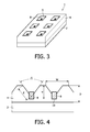
- the recesses 6 are arranged as indentations, which are distributed evenly across the surface of the first fluorescent material 4.
- the recesses 6 have a bottom, within which a blind hole can be arranged.
- the blind hole on the bottom of the recesses 6 can be used to deposit the second fluorescent material 8.
- a sectional view of the recesses 6 is illustrated in Figure 4 .
- the second fluorescent material 8 is deposited within a blind hole 10 of the recess 6.
- the blind hole 10 is arranged on the bottom surface of the recess 6.
- the angle ⁇ is between 45° and 170°, preferably 90°.
- the size E is preferably 170 ⁇ m.
- the depth of the recess 6 and the blind hole 10 is preferably 180 ⁇ m.
- the overall thickness D is preferably 350 ⁇ m.
- the distance between two recesses 6 is preferably 0.5mm.
- the CCT may be adjusted.
- the distance between the at least two recesses may be chosen to be 0,1-1mm, preferably 0,5 mm.
- the recesses may be formed in the surface of the first fluorescent material comb-shaped.
- the depth of each recess may be 180 ⁇ m and the thickness of the first fluorescent material may be 350 ⁇ m.
- the comb-shaped recess can be formed by pyramids on the surface of the first fluorescent material. The peaks of the pyramids may be cut-off.
- the second fluorescent material may be arranged within the at least one recess of the surface of the first fluorescent material such that the composition of the first light, the second light and the third light has a color rendering index higher than 80 at a correlated color temperature of less than 6000 K, preferably less than 5000 K.
- the depth of the at least one recess may be at least half the thickness of the first fluorescent material.
- the second fluorescent material is arranged close to the radiation source.
- the third light may radiate in the direction of light without interference by the first fluorescent material.
- the second light may radiate in the direction of light without interference by the second fluorescent material.
- embodiments provide the at least one recess with an opening angle of between 45° and 120°, preferably 90°.
- the illustrated arrangement of the second fluorescent material 8 in the recess 6, enables absorbing only a minimal amount of light emitted from the first fluorescent material 4.
- the second fluorescent material is arranged close to the LED 2, such that already the light from the LED 2 excites the second fluorescent material 8.
- the pyramidal formed opening in the first fluorescent material 4 allow the light emitted from the second fluorescent material to emit without distortion into the direction of light.
- the recess may be comb-shaped. Each of the recess may have a pyramidal shape. The peaks of the pyramids may be cut-off providing an even surface on the first fluorescent material 4.
- FIGS 5-7 illustrate emission and absorption spectra. Illustrated are normalized emission spectra of LED 2 (12), of first fluorescent material 4 (14), and second fluorescent material 8 (16). In addition, absorption spectra (k) of first fluorescent material 4 (18) and of second fluorescent material 8 (20) are illustrated..
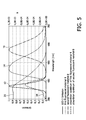
- Figure 5 illustrates an emission spectrum 16 of a second fluorescent material 8 Ca 1-x Sr x AlSiN 3 :Eu, wherein 0 ⁇ x ⁇ 1 and emission spectrum 14 from a YAG:Ce (0,3%) garnet as first fluorescent material 4.
- the respective absorption spectrum 20 of second fluorescent material 8 Ca 1-x Sr x AlSiN 3 :Eu, wherein 0 ⁇ x ⁇ 1 and absorption spectrum 18 from a YAG:Ce (0,3%) garnet as first fluorescent material 4 are shown.
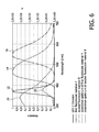
- Figure 6 illustrates an emission spectrum 16 of a second fluorescent material 8 Sr 2-y Si 5-x Al x N 8-x O x :Eu y , wherein 0 ⁇ x ⁇ 2, 0.005 ⁇ y ⁇ 0.05, and emission spectrum 14 from a YAG:Ce (0,2%) garnet as first fluorescent material 4.
- the respective absorption spectrum 20 of second fluorescent material 8 Sr 2-y Si 5-x Al x N 8-x Ox:Eu y wherein 0 ⁇ x ⁇ 2, 0.005 ⁇ y ⁇ 0.05, and absorption spectrum 18 from a YAG:Ce (0,2%) garnet as first fluorescent material 4 are shown.
- Figure 7 illustrates an emission spectrum 16 of a second fluorescent material 8 Sr 2-x Si 5 N 8 :Eu x , wherein 0.005 ⁇ x ⁇ 0.05, and emission spectrum 14 from a YAG:Ce (0,5%) garnet as first fluorescent material 4.
- the respective absorption spectrum 20 of second fluorescent material 8 Sr 2-x Si 5 N 8 :Eu x , wherein 0.005 ⁇ x ⁇ 0.05, and absorption spectrum 18 from a YAG:Ce (0,5%) garnet as first fluorescent material 4 are shown.
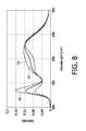
- Figure 8 illustrates emission spectra of lighting system 1 according to embodiments.
- Graph 22 illustrates an emission spectrum of a lighting system as illustrated in Figure 2 .
- Graph 26 illustrates an emission spectrum of a lighting system as illustrated in Figure 1 .
- Graph 24 illustrates an emission spectrum of a lighting system wherein the second fluorescent material 8 is sandwiched between the LED 2 and the first fluorescent material 4.
- the inventive arrangement of recesses and depositions provides the creation of white light with a CRI of above 80 at a color temperature of less than 6000K, preferably less than 5000K.
Description
- The present patent application relates generally to phosphor-converted semiconductor light emitting devices.
- Semiconductor light-emitting devices including light emitting diodes (LEDs) are among the most efficient light sources currently available. LEDs in use are capable of operating in the whole visible spectrum. The LEDs may be produced using semiconductors, including the Group of III-V semiconductors, particularly binary, ternary, and quaternary alloys of gallium, aluminum, indium, and nitrogen, also referred to as III-nitride materials.
- LEDs are commonly used in various different illumination systems, for example, for lighting, atmosphere lighting, advertisement lighting, etc. In order to provide a good lighting impression, illumination systems using UV-LEDs have been proposed, where the light emitted from the UV-LED is converted by means of a fluorescent material.
- Since blue-UV light has higher photon energy, i.e. a shorter wavelength, relative to other colors of visible light, such light can be readily converted to produce light having a longer wavelength. It is well known in the art that light having a first peak wavelength ("first light") can be converted into light having a longer peak wavelength ("second/third light") using a process known as luminescence. The luminescence process involves absorbing the first light by a photoluminescent material (also called phosphors), which excites the atoms of the material, and emits the second light. The peak wavelength and the band of wavelengths around it, may be called wavelength, in short. The wavelength of the second light will depend on the photoluminescent material. The type of photoluminescent material can be chosen to yield secondary light having a particular peak wavelength.
- To improve a color-rendering index (CRI) of lighting systems using LEDs, a dichromatic illumination system has already been proposed. In such a system, the primary emission of a blue LED is combined with light emitted by a photoluminescent material, for example a yellow phosphor. For example, a Y3Al5O12:Ce3+ phosphor is used as a photoluminescent material. A portion of the blue light emitted from the LED is converted to yellow light by the phosphor. Another portion of the blue light from the LED is transmitted through the phosphor. Thus, this system emits both blue light emitted from the LED, and yellow light emitted from the phosphor. The mixture of blue and yellow emission bands are perceived as white light by an observer. The perceived light has a CRI between 70 and 80 and a color temperature that ranges from about 5000 K to about 8000 K.
- Nevertheless, in many lighting applications, the CRI of less than 80 is not acceptable. For example, in business lighting, in atmosphere lighting, etc., white light LEDs based on the dichromatic approach can often not be used, because the CRI is poor, caused by the absence of red color components. In particular, for color temperatures below 5000 K as used in general illumination, the CRI is below 70 with the dichromatic blue - yellow LED lighting system.
- In order to further improve the CRI even at high correlated color temperatures (CCT), i.e. CCT<6000, a wavelength converted semiconductor light emitting device has been proposed, where a first wavelength converting material and a second wavelength converting material is provided. CCT of a light source may be understood according to the color coordinates of a Planckian Emitter with said temperature with minimum distance to the color point of the light source in CIE u-v system from 1960.
- The first wavelength converting material (fluorescent material) emits light having a shorter wavelength than light emitted by the second wavelength converting material.
- Document
JP2006032726 A - The first and second wavelength converting materials may be deposited on the light emitting device. However, within the known devices, the efficacy is poor because the first and second wavelength converting materials are intermixed resulting in strong back-scattering and loss of light. Further, the second wavelength converting material is often only excited by the light emitted from the first wavelength converting material. Further, the adjustment of the desired correlated color temperature (CCT) is very poor.
- Therefore, it is an object of the present application to provide a lighting system emitting white light with a high CRI. It is another object of the application to provide a lighting system, which has a high efficacy, a well-defined color temperature and good lighting properties. It is another object of the present application to provide LED lighting with a warm white light emission, i.e. CCT < 6000 K. Another object of the application is to allow adjusting the CCT of a lighting system.
- These and other objects are solved by a light emitting system comprising a radiation source capable of emitting a first light of at least a first wavelength spectrum, a first fluorescent material layer being arranged on a surface of the radiation source and being capable of absorbing at least partially the first light and emitting second light having a second wavelength spectrum, a second fluorescent material capable of absorbing at least partially the first light and emitting a third light having a third wavelength spectrum, wherein the first fluorescent material layer is a polycrystalline ceramics with a density of more than 97 percent of the density of a monocrystalline material and wherein the respective other fluorescent material is a phosphor powder with a median particle size 100nm < d50% <50 µm.
- It is noted that the published patent application
US2004/0145308 _discloses a light source having at least one LED for emitting primary radiation and at least one luminescence conversion body having at least one luminescent material for converting the primary radiation into a secondary radiation. The luminescence conversion body is a polycrystalline ceramic body with a ceramic density of more than 97 percent. - A monocrystalline material may be understood as a crystalline solid phase in which the crystal lattice of the entire sample is continuous, non-distorted and unbroken to the edges of the sample, with no grain boundaries. Its density is 100%.
- Polycrystals may be made up of a number of smaller crystals known as crystallites. The density of the polycrystals may be defined by the number of pores, glass phases or extrinsic phases. The term "polycrystalline material" may be understood as a material with a volume density larger than 90 percent of the main constituent, consisting of more than 80 percent of single crystal domains, with each domain being larger than 0.5 µm in diameter and having different crystallographic orientations. The single crystal domains may be connected by amorphous or glassy material or by additional crystalline constituents.
- The phosphor powder may comprise monocrystals and polycrystals. It has been found that the combination of a polycrystalline ceramics with a density of more than 97 percent of the density of a monocrystalline material with identical composition with a phosphor powder provides high mechanic stability and at the same time a good CRI.
- The high density material may be understood as a ceramic. It may have ≥ 95 % to ≤ 100 % of the theoretical density. Thus, the ceramic provides greatly improved mechanical and optical characteristics compared to materials with less density. Preferably, the ceramic material has ≥ 97 % to ≤ 100 % of the theoretical density, more preferred ≥ 98 % to ≤ 100 %.
- The radiation source may be a LED emitting light with a short wavelength, preferably in the UVA to blue spectral region, for example between about 330 nm and about 470 nm. Other radiation sources emitting high energy light are also possible. The fluorescent materials completely or partially absorb the light from the radiation source and emit it again in other spectral regions in a sufficiently broad band, and by use of the second fluorescent material with a significant proportion of red. An overall emission with the desired white color temperature and CRI is formed.
- The first fluorescent material, which converts the wavelength of the first light, may be a cerium doped polycrystalline ceramic body. The ceramic may, for example, be a cerium doped YAG:Ce(0,5%) garnet. The first fluorescent material may emit light in the yellow-green spectrum. The first fluorescent material may be excited by the first light. For example, a green-yellow emitting cerium-praseodymium-activated lutetium-yttrium-aluminum-gallium-scandium garnet phosphor of general formula (Lu1-x-yYxGdy)3-a-b(Al1-m-nGamScn)5O12:CeaPrb) with 0 ≤ x ≤ 1, 0 ≤ y ≤ 0.5, 0.001 ≤ a ≤ 0.02, 0.001 ≤ b ≤ 0.005, 0 ≤ m ≤ 0.5, and 0 ≤ n ≤ 0.5 may be used. For example, the garnet material may have preferred compositions of (Lu0.2Y0.8)2.994(Al4.95Sc0.05)O12:Ce0.006 or (Y0.9Gd0.1)2.994Al5O12:Ce0.006. The examples may also include compositions that deviate from the ideal garnet stoichiometry, for example, (Y0.9Gd0.1)2.994Al5.01O12.015:Ce0.006. Most preferably, compositions that show a deviation from ideal stoichiometry are single phase. The examples may also include compositions with additional components that can be traced back to the use of sintering fluxes like borates, silicon oxides, silicates, alkaline earth compounds, fluorides, or nitrides like aluminum nitride or silicon nitride. These additional components may be dissolved in the ceramic garnet grains or may be present as secondary phases like grain boundary phases.
- The second fluorescent material may be, for example, a red-emitting phosphor, such as a red emitting europium-activated phosphor. The second fluorescent material may be selected from the group of (Ca1-x-ySrx)S:Euy with 0 ≤ x ≤ 1, 0.0003 ≤ y ≤ 0.01; (Ba1-x-ySrxCay)2-zSi5-aAlaN8-aOa:Euz with 0 ≤ x 0.5, 0 ≤ y ≤ 0.8, 0.0025 ≤ z ≤ 0.05, 0 ≤ a ≤ 1; or (Ca1-x-ySrxMgy)1-zSi1-aAl1+aN3-aOa:Euz with 0 ≤ x 0.5, 0 ≤ y ≤ 0.2, 0.003 ≤ z ≤ 0.05, 0 ≤ a ≤ 0.02. Preferably, a europium activated calcium aluminum silicon nitride of composition Ca0.98Si0.985Al1.015N2.99O0.01:Eu0.02 is used, which is a high chromaticity red phosphor excitable from the near UV (400 nm) to the blue-green (500 nm) with high quantum efficiency. For an optimized use of this phosphor for luminescent conversion of primary LED light, it is necessary to modify the photophysical characteristics to achieve, for example, efficacy, color specifications and lifetime of related light emitting devices. The chromaticity and quantum efficiency of the europium activated calcium aluminum silicon nitride can be modified through the substitution of divalent metal ions for calcium from the list including Ba, Sr, Mg, by changing the N/O and Al/Si ratio in the lattice. Most preferably, the red emitting europium activated calcium aluminum silicon nitride material is produced by cofiring with a halide flux added such as ammonium chloride or sodium chloride. The halide flux lowers the required firing temperature of the phosphor and greatly improves the light output of the material. Most of the residual flux may be washed out after firing, however, small amounts may be incorporated in the lattice without deteriorating the luminescence properties leading to formulations such as Ca0.98Si0.985A11.015N2.99O0.01:Eu0.02Clx, x < 0.0015 or Cao.96Nao.o2SiAlN2.980o.o2:Euo.o2Clx, x < 0.0015.
- The second fluorescent material is arranged within at least one recess, preferably more than two recesses, within the first fluorescent material layer and having an opening in a surface of the first fluorescent material layer facing away from the radiation source. This may result in that the third light having the third wavelength spectrum is excited predominantly by the first light. The recesses may be pits, grooves, dents, cavities, indentation or the like. The at least one recess is arranged on a surface of the first fluorescent material layer facing away from the radiation source. The recesses may be arranged in compartments.
- In an alternative arrangement, the first fluorescent material may have at least one flat surface with the second fluorescent material forming a second luminescent layer on said flat surface. Preferably, the second fluorescent layer is scattering light. The second fluorescent material, which converts the wavelength of the first and the second light, is arranged within the recess. The second fluorescent material may be arranged within the at least one recess as balls, accumulations, clusters, beadings, cubes, and the like.
- By arranging the second fluorescent material in the at least one recess, the second light emitted from the first fluorescent material is only minimally absorbed. The light from the first fluorescent material is emitted with minimized re-absorption by the second fluorescent material. In addition, the second fluorescent material is arranged close to the radiation source, such that already the first light excites the second fluorescent material and light emitted from the first luminescent material is not transmitted through the second luminescent material.
- The quality in rendering illuminated colors of a white light emitting radiation source, which is indicated as the color rendering index (CRI), should be improved by a lighting system according to embodiments. A CRI of 100 is an indication that the light emitted from the light source is identical to that from a black body source, i.e. an incandescent or halogen lamp for CCT < 5000 K in the visible spectral range from 380 - 780 nm or identical to a sun-like spectrum as defined by CIE Pub 13.3 (CIE 13.3:1995, Method of Measuring and Specifying Colour Rendering Properties of Light Sources.).
- By arranging the layer thickness, the size and dimension of the recess, the CCT and CRI may be adjusted. For example, the distance between the at least two recesses may be chosen to be 0,1-1mm, preferably 0,5 mm. The recesses may be formed in the surface of the first fluorescent material comb-shaped. The depth of each recess is at least half the thickness of the first fluorescent material. It is preferred that the recess has a depth of 20 µm. The thickness D of the at least one polycrystalline fluorescent material layer is 50 µm < D < 850µm, preferably 80 µm < D < 250 µm. The comb-shaped recesses can be formed by pyramids on the surface of the first fluorescent material. The peaks of the pyramids may be cut-off.
- According to embodiments, the second fluorescent material may be arranged at at least one surface of the first fluorescent material such that the composition of the first light, the second light and the third light has a color rendering index higher than 80 at a correlated color temperature of less than 6000 K, preferably less than 5000 K.
- For example the layer formed by the second fluorescent material formed on at least one surface of the first luminescent material has a scattering coefficient s in the range of 30cm-1 <s<1000cm-1. Such a layer may consist of a phosphor particles with a median diameter d50% of 0.5µm<d50%<20µm. The depth of the at least one recess is at least half the thickness of the first fluorescent material, preferably 20µm. By that, the second fluorescent material is arranged close to the radiation source and the light from the first luminescent material may radiate without interference by the second fluorescent material. For enabling direct excitation of the second fluorescent material by the LED light source, embodiments provide the at least one recess with an opening angle of between 15° and 160°, preferably 90°.
- Another aspect of the application is a lighting device comprising a previously described light emitting system.
- These and other aspect of the application will become apparent from and elucidated with reference to the following figures.
-
FIG. 1 illustrates a side view of a first embodiment of a lighting system; -
FIG. 2 illustrates a perspective view of a second embodiment of a lighting system; -
FIG. 3 illustrates a perspective view of a third embodiment of a lighting system; -
FIG. 4 illustrates a sectional view of embodiments of a lighting system; -
FIG. 5 illustrates emission and absorption spectra of the components of a lighting system according to embodiments; -
FIG. 6 illustrates another emission and absorption spectra of the components of a lighting system according to embodiments; -
FIG. 7 illustrates another emission and absorption spectra of the components of a lighting system according to embodiments; -
FIG. 8 illustrates emission spectra for different arrangements of lighting system according to embodiments. -
Figure 1 illustrates a side view onto alighting system 1 according to an exemplary device not according to the current invention. Thesystem 1 may comprise aradiation source 2, which may be, for example, a blue light emitting LED. Arranged on the surface of theLED 2 is a firstfluorescent material 4. The firstfluorescent material 4 has a flat surface on which a secondfluorescent material 8 is deposited. Thefirst fluorescent 4 material is preferably a polycrystalline ceramics with a density of more than 97 percent of the density of a monocrystalline material. The secondfluorescent material 8 is preferably a powder. The powder may have a median particle d50% size between 100nm < d50%<50 µm. The powder may be applied onto the surface of the first fluorescent material by dusting, electrostatic dusting or so-called photo-tacky processes. It may also be possible to a apply thesecond fluorescent 8 material as a foil composed of a binder material with phosphor and to deposit the foil with the second fluorescent material onto the radiation source with said first luminescent material. -
Figure 2 illustrates a perspective view onto alighting system 1 according to embodiments. Thesystem 1 may comprise a radiation source, which may be, for example, an UV-LED 2. Arranged on the surface of theLED 2 is a firstfluorescent material 4. The firstfluorescent material 4 hasrecesses 6, in which a secondfluorescent material 8 is deposited. - The used
fluorescent material fluorescent materials - Radiation sources include semiconductor optical radiation emitters and other devices that emit optical radiation in response to electrical excitation. Semiconductor optical radiation emitters include light emitting diode LED chips, light emitting polymers (LEPs), organic light emitting devices (OLEDs), polymer light emitting devices (PLEDs), etc.
- Moreover, light emitting components such as those found in discharge lamps and fluorescent lamps, such as mercury low and high pressure discharge lamps, sulfur discharge lamps, and discharge lamps based on molecular radiators are also contemplated for use as radiation sources. Particularly good results are achieved with a
blue LED 2 whose emission maximum lies at 400 to 480 nm. Optimal ranges have been found to lie at 440 to 460 nm and 438 to 456 nm, taking particular account of the excitation spectrum of thefluorescent materials - The first
fluorescent material 4 may be a green/yellow-emitting garnet. For example, Ce3+ (preferably 0.15%) doped Y3Al5O12 is useful for applications requiring white light. The narrow excitation spectrum of conventional Y3Al5O12:Ce3+ leads to a gap in the combined spectrum between the emission of theLED 2 and the emission of the firstfluorescent material 4. Widening the excitation spectrum permits the use of aLED 2 emitting light of a wavelength that can at least partially fill the spectrum gap, which potentially has a favorable effect on the color rendering of the composite light emitted by the device. Though in the above discussion of the first embodiment the garnet host Y3Al5O12 is specifically mentioned, it is to be understood that garnet fluorescent materials having the general formula (Lu1-x-yYxGdy)3-a-b(Al1-m-nGamScn)5O12:CeaPrb) with 0 ≤ x ≤ 1,0 ≤ y ≤ 0.5, 0.001 ≤ a ≤ 0.02, 0.001 ≤ b ≤ 0.005, 0 ≤ m ≤ 0.5, and 0 ≤ n ≤ 0.5 may also be used. This class of fluorescent material is based on activated luminescence of cubic garnet crystals. Garnets are a class of materials with the crystal chemical formula A3B5X12. A atoms may be chosen from the group comprising Y, Gd, Lu, Tb, Yb, La, Ca, Sr, B atoms may be chosen from the group comprising Al, Mg, Sc, B, Ga, Si, Ge, In, and X atoms may be chosen from the group comprising O, N, F, S. Part of the A atoms may be substituted by the doping atoms chosen from the group comprising Ce, Pr, Sm, Eu, Dy, Ho, Er, Tm. The doping concentration may be in the range 0.01 - 10 mole% with respect to the A atoms, most preferably in the range 0.1 - 2 mole%. - The second
fluorescent material 8 may be a red-emitting phosphor. Examples of suitable red-emitting phosphors include Ca1x-ySrxAlSiN3:Euy, or Sr2-xSi5N8:Eux, wherein 0.005<x<0.05, or Sr2-ySi5-xAlxN8-xOx:Euy, wherein 0<x<2, 0.005<y<0.05, or Ba2-x-ySrxSi5N8:Euy, wherein 0<x<1, 0.005<y<0.05. - The light emitted from
LED 2 is converted in its wavelength by both the firstfluorescent material 4 and the secondfluorescent material 8. Blue light emitted by theLED 2 mixes with green and red light emitted by firstfluorescent material 4 and the secondfluorescent material 8 to make white light. The CCT and CRI of the white light may be controlled by controlling the design of the firstfluorescent material 4 and the secondfluorescent material 8. - The patterns of
fluorescent material fluorescent material 4, i.e. using mechanical grinding and sawing techniques, conventional lithography and etching techniques, depositing the secondfluorescent material 8, i.e. by electrophoretic deposition. Alternatively, patterns and layers of fluorescent material may be deposited by screen printing or ink jet printing or dusting, electrostatic dusting or so-called photo-tacky processes. Eventually, the package of firstfluorescent material 4 and secondfluorescent material 8 may be placed onto theLED 2. - According to embodiments, the second
fluorescent material 8 is deposited inrecesses 6 of the firstfluorescent material 4. Therecesses 6 can be formed as pits, grooves, dents, cavities, indentation. As illustrated inFigure 1 , the recesses are arranged in grooves, which are parallel to each other along the length of the first fluorescent material. - Another arrangement according to embodiments is illustrated in
Figure 3 . As can be seen, therecesses 6 are arranged as indentations, which are distributed evenly across the surface of the firstfluorescent material 4. Therecesses 6 have a bottom, within which a blind hole can be arranged. The blind hole on the bottom of therecesses 6 can be used to deposit the secondfluorescent material 8. - A sectional view of the
recesses 6 is illustrated inFigure 4 . The secondfluorescent material 8 is deposited within ablind hole 10 of therecess 6. Theblind hole 10 is arranged on the bottom surface of therecess 6. The angle α is between 45° and 170°, preferably 90°. The size E is preferably 170 µm. The depth of therecess 6 and theblind hole 10 is preferably 180 µm. The overall thickness D is preferably 350 µm. The distance between tworecesses 6 is preferably 0.5mm. - By arranging the size and dimension of the recess, the CCT may be adjusted. For example, the distance between the at least two recesses may be chosen to be 0,1-1mm, preferably 0,5 mm. The recesses may be formed in the surface of the first fluorescent material comb-shaped. The depth of each recess may be 180 µm and the thickness of the first fluorescent material may be 350 µm. The comb-shaped recess can be formed by pyramids on the surface of the first fluorescent material. The peaks of the pyramids may be cut-off.
- According to embodiments, the second fluorescent material may be arranged within the at least one recess of the surface of the first fluorescent material such that the composition of the first light, the second light and the third light has a color rendering index higher than 80 at a correlated color temperature of less than 6000 K, preferably less than 5000 K.
- For example, the depth of the at least one recess may be at least half the thickness of the first fluorescent material. By that, the second fluorescent material is arranged close to the radiation source. The third light may radiate in the direction of light without interference by the first fluorescent material. In addition, the second light may radiate in the direction of light without interference by the second fluorescent material.
- For enabling free radiation of third light into the direction of light, embodiments provide the at least one recess with an opening angle of between 45° and 120°, preferably 90°. The illustrated arrangement of the second
fluorescent material 8 in therecess 6, enables absorbing only a minimal amount of light emitted from the firstfluorescent material 4. In addition, the second fluorescent material is arranged close to theLED 2, such that already the light from theLED 2 excites the secondfluorescent material 8. The pyramidal formed opening in the firstfluorescent material 4 allow the light emitted from the second fluorescent material to emit without distortion into the direction of light. As can be seen fromFigure 4 , the recess may be comb-shaped. Each of the recess may have a pyramidal shape. The peaks of the pyramids may be cut-off providing an even surface on the firstfluorescent material 4. -
Figures 5-7 illustrate emission and absorption spectra. Illustrated are normalized emission spectra of LED 2 (12), of first fluorescent material 4 (14), and second fluorescent material 8 (16). In addition, absorption spectra (k) of first fluorescent material 4 (18) and of second fluorescent material 8 (20) are illustrated.. -
Figure 5 illustrates anemission spectrum 16 of a secondfluorescent material 8 Ca1-xSrxAlSiN3:Eu, wherein 0<x<1 andemission spectrum 14 from a YAG:Ce (0,3%) garnet as firstfluorescent material 4. Therespective absorption spectrum 20 of secondfluorescent material 8 Ca1-xSrxAlSiN3:Eu, wherein 0<x<1 andabsorption spectrum 18 from a YAG:Ce (0,3%) garnet as firstfluorescent material 4 are shown. -
Figure 6 illustrates anemission spectrum 16 of a secondfluorescent material 8 Sr2-ySi5-xAlxN8-xOx:Euy, wherein 0<x<2, 0.005<y<0.05, andemission spectrum 14 from a YAG:Ce (0,2%) garnet as firstfluorescent material 4. Therespective absorption spectrum 20 of secondfluorescent material 8 Sr2-ySi5-xAlxN8-xOx:Euy, wherein 0<x<2, 0.005<y<0.05, andabsorption spectrum 18 from a YAG:Ce (0,2%) garnet as firstfluorescent material 4 are shown. -
Figure 7 illustrates anemission spectrum 16 of a secondfluorescent material 8 Sr2-xSi5N8:Eux, wherein 0.005<x<0.05, andemission spectrum 14 from a YAG:Ce (0,5%) garnet as firstfluorescent material 4. Therespective absorption spectrum 20 of secondfluorescent material 8 Sr2-xSi5N8:Eux, wherein 0.005<x<0.05, andabsorption spectrum 18 from a YAG:Ce (0,5%) garnet as firstfluorescent material 4 are shown. -
Figure 8 illustrates emission spectra oflighting system 1 according to embodiments.Graph 22 illustrates an emission spectrum of a lighting system as illustrated inFigure 2 .Graph 26 illustrates an emission spectrum of a lighting system as illustrated inFigure 1 . Eventually,Graph 24 illustrates an emission spectrum of a lighting system wherein the secondfluorescent material 8 is sandwiched between theLED 2 and the firstfluorescent material 4. - The inventive arrangement of recesses and depositions provides the creation of white light with a CRI of above 80 at a color temperature of less than 6000K, preferably less than 5000K.
Claims (8)
- A light emitting system (1) comprising:a radiation source (2) capable of emitting a first light of at least a first wavelength spectrum;a first fluorescent material layer (4) being arranged on a surface of the radiation source (2) and being capable of absorbing at least partially the first light and emitting second light having a second wavelength spectrum, wherein the first fluorescent material layer (4) is a polycrystalline ceramic with a density of more than 97 percent of the density of a monocrystalline material,a second fluorescent material (8) being capable of absorbing at least partially the first light and emitting a third light having a third wavelength spectrum, characterized bythe second fluorescent material (8) being a phosphor powder with a median particle size 100 nm < d50%<50 µm,at least one recess (6) being arranged on a surface of the first fluorescent material layer (4) and having an opening in a surface of the first fluorescent material layer (4) facing away from the radiation source (2), the second fluorescent material (8) being arranged within the at least one recess (6) wherein the depth of the at least one recess (6) is at least half the thickness of the first fluorescent material layer.
- The light emitting system (1) of claim 1, wherein the at least one recess (6) has a blind hole (10) at the deepest part thereof, the second fluorescent material (8) is deposited within the blind hole (10), and the opening angle of the at least one recess is between 45° and 170 °.
- The light emitting system (1) of claim 1, wherein the at least one recess is formed by a pyramid or a pyramid with a cut-off peak.
- The light emitting system (1) of claim 1, wherein the thickness D of the first fluorescent material layer is 50µm < D < 850µm.
- The light emitting system (1) of claim 1, wherein the at least one recess (6) has an opening angle of between 15° and 160°, preferably 90°.
- The light emitting system (1) of claim 1, having a plurality of recesses (6) and wherein the distance between two of the recesses (6) is 0.1mm- 1mm, preferably 0.5 mm.
- The light emitting system (1) of claim 1, wherein said first fluorescent material (4) comprises a phosphor having the formula (Lu1-x-yYxGdy)3-a-b(All-m-nGamScn)5O12:CeaPrb) with 0 ≤ x ≤ 1,0 ≤ y ≤ 0.5, 0.001 ≤ a ≤ 0.02, 0.001 ≤ b ≤ 0.005, 0 ≤ m ≤ 0.5, and 0 ≤ n ≤0.5.
- The light emitting system (1) of claim 1, wherein the second fluorescent material (8) is selected from the group ofA) (Ca1-x-ySrx)S:Euywith 0 ≤ x ≤ 1, 0.0003 ≤ y ≤ 0.01;B) (Ba1-x-ySrxCay)2-zSi5-aAlaN8-aOa:Euz with 0 ≤ x ≤ 0.5, 0 ≤ y ≤ 0.8, 0.0025 ≤ z ≤ 0.05, 0 ≤ a ≤ 1; forC) (Ca1-x-ySrxMgy)1-zSi1-aAl1+aN3-aOa:Euz with 0 ≤ x ≤ 0.5, 0 ≤ y ≤ 0.2, 0.003 ≤ z ≤ 0.05, 0 ≤ a ≤ 0.02.
Priority Applications (1)
| Application Number | Priority Date | Filing Date | Title |
|---|---|---|---|
| EP07735438.9A EP2013918B1 (en) | 2006-04-25 | 2007-04-10 | Fluorescent lighting creating white light |
Applications Claiming Priority (3)
| Application Number | Priority Date | Filing Date | Title |
|---|---|---|---|
| EP06113086 | 2006-04-25 | ||
| EP07735438.9A EP2013918B1 (en) | 2006-04-25 | 2007-04-10 | Fluorescent lighting creating white light |
| PCT/IB2007/051271 WO2007122531A2 (en) | 2006-04-25 | 2007-04-10 | Fluorescent lighting creating white light |
Publications (2)
| Publication Number | Publication Date |
|---|---|
| EP2013918A2 EP2013918A2 (en) | 2009-01-14 |
| EP2013918B1 true EP2013918B1 (en) | 2015-02-11 |
Family
ID=38625382
Family Applications (1)
| Application Number | Title | Priority Date | Filing Date |
|---|---|---|---|
| EP07735438.9A Active EP2013918B1 (en) | 2006-04-25 | 2007-04-10 | Fluorescent lighting creating white light |
Country Status (8)
| Country | Link |
|---|---|
| US (1) | US8035287B2 (en) |
| EP (1) | EP2013918B1 (en) |
| JP (1) | JP5306992B2 (en) |
| KR (1) | KR101459999B1 (en) |
| CN (1) | CN101432897B (en) |
| RU (1) | RU2422945C2 (en) |
| TW (1) | TWI392829B (en) |
| WO (1) | WO2007122531A2 (en) |
Families Citing this family (40)
| Publication number | Priority date | Publication date | Assignee | Title |
|---|---|---|---|---|
| US8475683B2 (en) | 2006-10-20 | 2013-07-02 | Intematix Corporation | Yellow-green to yellow-emitting phosphors based on halogenated-aluminates |
| US8133461B2 (en) | 2006-10-20 | 2012-03-13 | Intematix Corporation | Nano-YAG:Ce phosphor compositions and their methods of preparation |
| US8529791B2 (en) | 2006-10-20 | 2013-09-10 | Intematix Corporation | Green-emitting, garnet-based phosphors in general and backlighting applications |
| US9120975B2 (en) | 2006-10-20 | 2015-09-01 | Intematix Corporation | Yellow-green to yellow-emitting phosphors based on terbium-containing aluminates |
| US8247828B2 (en) * | 2006-12-05 | 2012-08-21 | Koninklijke Philips Electronics N.V. | Illumination device, particularly with luminescent ceramics |
| US20100277673A1 (en) * | 2008-01-03 | 2010-11-04 | Koninklijke Philips Electronics N.V. | Display device and illumination device |
| US8567973B2 (en) | 2008-03-07 | 2013-10-29 | Intematix Corporation | Multiple-chip excitation systems for white light emitting diodes (LEDs) |
| WO2009141982A1 (en) * | 2008-05-19 | 2009-11-26 | 株式会社 東芝 | Linear white light source, and backlight and liquid crystal display device using linear white light source |
| CA2754433A1 (en) * | 2008-06-25 | 2009-12-30 | Mario W. Cardullo | Uv generated visible light source |
| US20120181919A1 (en) * | 2008-08-27 | 2012-07-19 | Osram Sylvania Inc. | Luminescent Ceramic Composite Converter and Method of Making the Same |
| DE102008050643B4 (en) * | 2008-10-07 | 2022-11-03 | OSRAM Opto Semiconductors Gesellschaft mit beschränkter Haftung | bulbs |
| TWI416757B (en) * | 2008-10-13 | 2013-11-21 | Advanced Optoelectronic Tech | Polychromatic wavelengths led and manufacturing method thereof |
| US8220971B2 (en) | 2008-11-21 | 2012-07-17 | Xicato, Inc. | Light emitting diode module with three part color matching |
| JP2010151851A (en) * | 2008-11-28 | 2010-07-08 | Toshiba Corp | Display device |
| TWI407595B (en) * | 2008-12-16 | 2013-09-01 | Gio Optoelectronics Corp | Manufacturing method of light-emitting apparatus |
| JP5887280B2 (en) * | 2010-02-03 | 2016-03-16 | コーニンクレッカ フィリップス エヌ ヴェKoninklijke Philips N.V. | Phosphor conversion LED |
| JP2012015254A (en) | 2010-06-30 | 2012-01-19 | Nitto Denko Corp | Phosphor ceramic and light emitting device |
| EP2596284A4 (en) | 2010-07-19 | 2015-04-29 | Rensselaer Polytech Inst | Full spectrum solid state white light source, method for manufacturing and applications |
| JP5519440B2 (en) * | 2010-08-03 | 2014-06-11 | 日東電工株式会社 | Light emitting device |
| US20120051045A1 (en) * | 2010-08-27 | 2012-03-01 | Xicato, Inc. | Led Based Illumination Module Color Matched To An Arbitrary Light Source |
| JP5861636B2 (en) * | 2010-08-31 | 2016-02-16 | 日亜化学工業株式会社 | Light emitting device and manufacturing method thereof |
| CN103314072A (en) | 2010-12-01 | 2013-09-18 | 皇家飞利浦电子股份有限公司 | Red emitting luminescent materials |
| KR20120088130A (en) * | 2011-01-31 | 2012-08-08 | 서울반도체 주식회사 | Light emitting device having wavelength converting layer and method of fabricating the same |
| JP5548629B2 (en) * | 2011-01-31 | 2014-07-16 | 古河機械金属株式会社 | Garnet crystal for scintillator and radiation detector using the same |
| RU2472252C1 (en) * | 2011-06-22 | 2013-01-10 | Государственное образовательное учреждение высшего профессионального образования Томский государственный университет систем управления и радиоэлектроники (ГОУ ВПО ТУСУР) | Method of making semiconductor light source |
| LT5918B (en) * | 2011-07-12 | 2013-03-25 | Vilniaus Universitetas | Polychromatic solid-staye light sources for the control of colour saturation of illuminated surfaces |
| CN102956799A (en) * | 2011-08-26 | 2013-03-06 | 亚德光机股份有限公司 | Light emitting device |
| DE102011113498A1 (en) | 2011-09-15 | 2013-03-21 | Osram Opto Semiconductors Gmbh | Phosphor mixture, optoelectronic component with a phosphor mixture and street lamp with a phosphor mixture |
| US8654414B2 (en) * | 2011-11-30 | 2014-02-18 | Lexmark International, Inc. | LED illumination system for a scanner including a UV light emitting device |
| RU2502917C2 (en) * | 2011-12-30 | 2013-12-27 | Закрытое Акционерное Общество "Научно-Производственная Коммерческая Фирма "Элтан Лтд" | Light diode source of white light with combined remote photoluminiscent converter |
| WO2013188687A1 (en) * | 2012-06-13 | 2013-12-19 | Innotec, Corp. | Illuminated accessory unit |
| KR20150100864A (en) * | 2012-12-28 | 2015-09-02 | 신에쓰 가가꾸 고교 가부시끼가이샤 | Phosphor-containing resin molded body, light emitting device, and resin pellet |
| JP6384893B2 (en) * | 2013-10-23 | 2018-09-05 | 株式会社光波 | Single crystal phosphor and light emitting device |
| JP6955704B2 (en) * | 2013-10-23 | 2021-10-27 | 株式会社光波 | Light emitting device |
| EP2947484B1 (en) * | 2014-05-14 | 2017-04-05 | Philips Lighting Holding B.V. | A light emitting device |
| TWI563207B (en) * | 2014-07-16 | 2016-12-21 | Playnitride Inc | Optical assembly and optical module |
| JP6356573B2 (en) * | 2014-10-23 | 2018-07-11 | 国立研究開発法人物質・材料研究機構 | Single crystal phosphor and light emitting device |
| CN107109216A (en) * | 2014-12-24 | 2017-08-29 | 皇家飞利浦有限公司 | The LED of phosphor converted |
| EP3241880B1 (en) * | 2016-05-03 | 2018-04-18 | Lumileds Holding B.V. | Wavelength converting material for a light emitting device |
| WO2018202534A1 (en) * | 2017-05-02 | 2018-11-08 | Philips Lighting Holding B.V. | Warm white led spectrum especially for retail applications |
Citations (1)
| Publication number | Priority date | Publication date | Assignee | Title |
|---|---|---|---|---|
| JP2006032726A (en) * | 2004-07-16 | 2006-02-02 | Kyocera Corp | Light emitting device |
Family Cites Families (21)
| Publication number | Priority date | Publication date | Assignee | Title |
|---|---|---|---|---|
| US3611069A (en) | 1969-11-12 | 1971-10-05 | Gen Electric | Multiple color light emitting diodes |
| US6686691B1 (en) * | 1999-09-27 | 2004-02-03 | Lumileds Lighting, U.S., Llc | Tri-color, white light LED lamps |
| US6621211B1 (en) | 2000-05-15 | 2003-09-16 | General Electric Company | White light emitting phosphor blends for LED devices |
| JP2002057376A (en) * | 2000-05-31 | 2002-02-22 | Matsushita Electric Ind Co Ltd | Led lamp |
| US6544438B2 (en) * | 2000-08-02 | 2003-04-08 | Sarnoff Corporation | Preparation of high emission efficiency alkaline earth metal thiogallate phosphors |
| JP2002141559A (en) * | 2000-10-31 | 2002-05-17 | Sanken Electric Co Ltd | Light emitting semiconductor chip assembly and light emitting semiconductor lead frame |
| JP2002299691A (en) * | 2001-04-04 | 2002-10-11 | Seiwa Electric Mfg Co Ltd | Light emitting diode lamp and filter used therefor |
| JP3948650B2 (en) | 2001-10-09 | 2007-07-25 | アバゴ・テクノロジーズ・イーシービーユー・アイピー(シンガポール)プライベート・リミテッド | Light emitting diode and manufacturing method thereof |
| JP4087093B2 (en) * | 2001-10-15 | 2008-05-14 | 株式会社日立メディコ | Phosphor element, radiation detector using the same, and medical image diagnostic apparatus |
| US7768189B2 (en) * | 2004-08-02 | 2010-08-03 | Lumination Llc | White LEDs with tunable CRI |
| US7554258B2 (en) | 2002-10-22 | 2009-06-30 | Osram Opto Semiconductors Gmbh | Light source having an LED and a luminescence conversion body and method for producing the luminescence conversion body |
| JP3717480B2 (en) | 2003-01-27 | 2005-11-16 | ローム株式会社 | Semiconductor light emitting device |
| US7038370B2 (en) | 2003-03-17 | 2006-05-02 | Lumileds Lighting, U.S., Llc | Phosphor converted light emitting device |
| US7250715B2 (en) | 2004-02-23 | 2007-07-31 | Philips Lumileds Lighting Company, Llc | Wavelength converted semiconductor light emitting devices |
| JP4535236B2 (en) * | 2004-03-10 | 2010-09-01 | 株式会社ファインラバー研究所 | Fluorescent member, fluorescent member manufacturing method, and semiconductor light emitting device |
| US7635668B2 (en) * | 2004-03-16 | 2009-12-22 | The Lubrizol Corporation | Hydraulic composition containing a substantially nitrogen free dispersant |
| TW200604325A (en) * | 2004-03-22 | 2006-02-01 | Fujikura Ltd | Light-emitting device and illuminating device |
| JP2005298696A (en) * | 2004-04-13 | 2005-10-27 | Fujikura Ltd | Method for producing fluorophor powder, fluorophor powder and visible wavelength light-emitting device |
| US7462086B2 (en) | 2004-04-21 | 2008-12-09 | Philips Lumileds Lighting Company, Llc | Phosphor for phosphor-converted semiconductor light emitting device |
| US7361938B2 (en) * | 2004-06-03 | 2008-04-22 | Philips Lumileds Lighting Company Llc | Luminescent ceramic for a light emitting device |
| JP2007018222A (en) * | 2005-07-07 | 2007-01-25 | Matsushita Electric Ind Co Ltd | Memory access control circuit |
-
2007
- 2007-04-10 KR KR1020087028647A patent/KR101459999B1/en active IP Right Grant
- 2007-04-10 RU RU2008146391/28A patent/RU2422945C2/en active
- 2007-04-10 US US12/298,061 patent/US8035287B2/en active Active
- 2007-04-10 JP JP2009507201A patent/JP5306992B2/en active Active
- 2007-04-10 EP EP07735438.9A patent/EP2013918B1/en active Active
- 2007-04-10 WO PCT/IB2007/051271 patent/WO2007122531A2/en active Application Filing
- 2007-04-10 CN CN2007800151349A patent/CN101432897B/en active Active
- 2007-04-20 TW TW096114141A patent/TWI392829B/en active
Patent Citations (1)
| Publication number | Priority date | Publication date | Assignee | Title |
|---|---|---|---|---|
| JP2006032726A (en) * | 2004-07-16 | 2006-02-02 | Kyocera Corp | Light emitting device |
Also Published As
| Publication number | Publication date |
|---|---|
| CN101432897A (en) | 2009-05-13 |
| EP2013918A2 (en) | 2009-01-14 |
| CN101432897B (en) | 2011-04-20 |
| JP5306992B2 (en) | 2013-10-02 |
| RU2008146391A (en) | 2010-06-10 |
| KR101459999B1 (en) | 2014-11-10 |
| WO2007122531A3 (en) | 2008-05-02 |
| TW200804720A (en) | 2008-01-16 |
| WO2007122531A8 (en) | 2008-10-23 |
| TWI392829B (en) | 2013-04-11 |
| KR20090013799A (en) | 2009-02-05 |
| US20090072710A1 (en) | 2009-03-19 |
| RU2422945C2 (en) | 2011-06-27 |
| US8035287B2 (en) | 2011-10-11 |
| JP2009534863A (en) | 2009-09-24 |
| WO2007122531A2 (en) | 2007-11-01 |
Similar Documents
| Publication | Publication Date | Title |
|---|---|---|
| EP2013918B1 (en) | Fluorescent lighting creating white light | |
| EP1566426B1 (en) | Phosphor converted light emitting device | |
| EP1859657B1 (en) | Illumination system comprising a radiation source and a fluorescent material | |
| US8771547B2 (en) | Oxycarbonitride phosphors and light emitting devices using the same | |
| JP5188687B2 (en) | Phosphor, manufacturing method thereof, and light emitting device | |
| US7038370B2 (en) | Phosphor converted light emitting device | |
| EP1411558B1 (en) | Phosphor converted light emitting device | |
| US6255670B1 (en) | Phosphors for light generation from light emitting semiconductors | |
| EP1893719B1 (en) | Illumination system comprising color deficiency compensating luminescent material | |
| TWI407474B (en) | A ceramic luminescence converter and illumination system comprising said converter | |
| TWI443854B (en) | Illumination system comprising a yellow green-emitting luminescent material | |
| JP5355547B2 (en) | White light source and luminescent material with improved color stability | |
| WO2007120582A1 (en) | WHITE LEDs WITH TAILORABLE COLOR TEMPERATURE | |
| JP2006169526A (en) | Phosphorescence converting light emitting device | |
| Dutta et al. | Inorganic phosphor materials for solid state white light generation | |
| CN112189045A (en) | High color-developing white light emitting device and high color-developing photoluminescent composition | |
| JP2014194019A (en) | Lighting system | |
| KR101176212B1 (en) | Alkali-earth Phosporus Nitride system phosphor, manufacturing method thereof and light emitting devices using the same | |
| JP2006104413A (en) | Phosphor and white light emitting device using the same | |
| KR100573858B1 (en) | Luminescence conversion light emitting diode comprising the sialon-based phosphors | |
| US9039933B2 (en) | Eu2+-activated aluminates nanobelts, whiskers, and powders, methods of making the same, and uses thereof | |
| EP3164463B1 (en) | Phosphor compositions and lighting apparatus thereof | |
| WO2022244523A1 (en) | Phosphor, method for producing same, light emitting element and light emitting device |
Legal Events
| Date | Code | Title | Description |
|---|---|---|---|
| PUAI | Public reference made under article 153(3) epc to a published international application that has entered the european phase |
Free format text: ORIGINAL CODE: 0009012 |
|
| 17P | Request for examination filed |
Effective date: 20081125 |
|
| AK | Designated contracting states |
Kind code of ref document: A2 Designated state(s): AT BE BG CH CY CZ DE DK EE ES FI FR GB GR HU IE IS IT LI LT LU LV MC MT NL PL PT RO SE SI SK TR |
|
| DAX | Request for extension of the european patent (deleted) | ||
| 17Q | First examination report despatched |
Effective date: 20130729 |
|
| RAP1 | Party data changed (applicant data changed or rights of an application transferred) |
Owner name: PHILIPS INTELLECTUAL PROPERTY & STANDARDS GMBH Owner name: KONINKLIJKE PHILIPS N.V. |
|
| REG | Reference to a national code |
Ref country code: DE Ref legal event code: R079 Ref document number: 602007040227 Country of ref document: DE Free format text: PREVIOUS MAIN CLASS: H01L0033000000 Ipc: H01L0033500000 |
|
| RIC1 | Information provided on ipc code assigned before grant |
Ipc: C09K 11/08 20060101ALI20131104BHEP Ipc: C09K 11/77 20060101ALI20131104BHEP Ipc: H01L 33/50 20100101AFI20131104BHEP |
|
| GRAP | Despatch of communication of intention to grant a patent |
Free format text: ORIGINAL CODE: EPIDOSNIGR1 |
|
| INTG | Intention to grant announced |
Effective date: 20140508 |
|
| GRAS | Grant fee paid |
Free format text: ORIGINAL CODE: EPIDOSNIGR3 |
|
| GRAA | (expected) grant |
Free format text: ORIGINAL CODE: 0009210 |
|
| AK | Designated contracting states |
Kind code of ref document: B1 Designated state(s): AT BE BG CH CY CZ DE DK EE ES FI FR GB GR HU IE IS IT LI LT LU LV MC MT NL PL PT RO SE SI SK TR |
|
| REG | Reference to a national code |
Ref country code: GB Ref legal event code: FG4D |
|
| REG | Reference to a national code |
Ref country code: CH Ref legal event code: EP |
|
| REG | Reference to a national code |
Ref country code: IE Ref legal event code: FG4D |
|
| REG | Reference to a national code |
Ref country code: AT Ref legal event code: REF Ref document number: 710163 Country of ref document: AT Kind code of ref document: T Effective date: 20150315 |
|
| REG | Reference to a national code |
Ref country code: DE Ref legal event code: R096 Ref document number: 602007040227 Country of ref document: DE Effective date: 20150326 |
|
| REG | Reference to a national code |
Ref country code: NL Ref legal event code: VDEP Effective date: 20150211 |
|
| REG | Reference to a national code |
Ref country code: AT Ref legal event code: MK05 Ref document number: 710163 Country of ref document: AT Kind code of ref document: T Effective date: 20150211 |
|
| REG | Reference to a national code |
Ref country code: LT Ref legal event code: MG4D |
|
| REG | Reference to a national code |
Ref country code: DE Ref legal event code: R082 Ref document number: 602007040227 Country of ref document: DE Representative=s name: MEISSNER, BOLTE & PARTNER GBR, DE Ref country code: DE Ref legal event code: R081 Ref document number: 602007040227 Country of ref document: DE Owner name: PHILIPS GMBH, DE Free format text: FORMER OWNER: PHILIPS INTELLECTUAL PROPERTY & STANDARDS GMBH, 20099 HAMBURG, DE Ref country code: DE Ref legal event code: R082 Ref document number: 602007040227 Country of ref document: DE Representative=s name: MEISSNER BOLTE PATENTANWAELTE RECHTSANWAELTE P, DE |
|
| PG25 | Lapsed in a contracting state [announced via postgrant information from national office to epo] |
Ref country code: FI Free format text: LAPSE BECAUSE OF FAILURE TO SUBMIT A TRANSLATION OF THE DESCRIPTION OR TO PAY THE FEE WITHIN THE PRESCRIBED TIME-LIMIT Effective date: 20150211 Ref country code: SE Free format text: LAPSE BECAUSE OF FAILURE TO SUBMIT A TRANSLATION OF THE DESCRIPTION OR TO PAY THE FEE WITHIN THE PRESCRIBED TIME-LIMIT Effective date: 20150211 Ref country code: ES Free format text: LAPSE BECAUSE OF FAILURE TO SUBMIT A TRANSLATION OF THE DESCRIPTION OR TO PAY THE FEE WITHIN THE PRESCRIBED TIME-LIMIT Effective date: 20150211 Ref country code: LT Free format text: LAPSE BECAUSE OF FAILURE TO SUBMIT A TRANSLATION OF THE DESCRIPTION OR TO PAY THE FEE WITHIN THE PRESCRIBED TIME-LIMIT Effective date: 20150211 |
|
| PG25 | Lapsed in a contracting state [announced via postgrant information from national office to epo] |
Ref country code: IS Free format text: LAPSE BECAUSE OF FAILURE TO SUBMIT A TRANSLATION OF THE DESCRIPTION OR TO PAY THE FEE WITHIN THE PRESCRIBED TIME-LIMIT Effective date: 20150611 Ref country code: AT Free format text: LAPSE BECAUSE OF FAILURE TO SUBMIT A TRANSLATION OF THE DESCRIPTION OR TO PAY THE FEE WITHIN THE PRESCRIBED TIME-LIMIT Effective date: 20150211 Ref country code: GR Free format text: LAPSE BECAUSE OF FAILURE TO SUBMIT A TRANSLATION OF THE DESCRIPTION OR TO PAY THE FEE WITHIN THE PRESCRIBED TIME-LIMIT Effective date: 20150512 Ref country code: NL Free format text: LAPSE BECAUSE OF FAILURE TO SUBMIT A TRANSLATION OF THE DESCRIPTION OR TO PAY THE FEE WITHIN THE PRESCRIBED TIME-LIMIT Effective date: 20150211 Ref country code: LV Free format text: LAPSE BECAUSE OF FAILURE TO SUBMIT A TRANSLATION OF THE DESCRIPTION OR TO PAY THE FEE WITHIN THE PRESCRIBED TIME-LIMIT Effective date: 20150211 |
|
| PG25 | Lapsed in a contracting state [announced via postgrant information from national office to epo] |
Ref country code: CZ Free format text: LAPSE BECAUSE OF FAILURE TO SUBMIT A TRANSLATION OF THE DESCRIPTION OR TO PAY THE FEE WITHIN THE PRESCRIBED TIME-LIMIT Effective date: 20150211 Ref country code: SK Free format text: LAPSE BECAUSE OF FAILURE TO SUBMIT A TRANSLATION OF THE DESCRIPTION OR TO PAY THE FEE WITHIN THE PRESCRIBED TIME-LIMIT Effective date: 20150211 Ref country code: DK Free format text: LAPSE BECAUSE OF FAILURE TO SUBMIT A TRANSLATION OF THE DESCRIPTION OR TO PAY THE FEE WITHIN THE PRESCRIBED TIME-LIMIT Effective date: 20150211 Ref country code: EE Free format text: LAPSE BECAUSE OF FAILURE TO SUBMIT A TRANSLATION OF THE DESCRIPTION OR TO PAY THE FEE WITHIN THE PRESCRIBED TIME-LIMIT Effective date: 20150211 Ref country code: RO Free format text: LAPSE BECAUSE OF FAILURE TO SUBMIT A TRANSLATION OF THE DESCRIPTION OR TO PAY THE FEE WITHIN THE PRESCRIBED TIME-LIMIT Effective date: 20150211 |
|
| REG | Reference to a national code |
Ref country code: DE Ref legal event code: R097 Ref document number: 602007040227 Country of ref document: DE |
|
| PG25 | Lapsed in a contracting state [announced via postgrant information from national office to epo] |
Ref country code: MC Free format text: LAPSE BECAUSE OF FAILURE TO SUBMIT A TRANSLATION OF THE DESCRIPTION OR TO PAY THE FEE WITHIN THE PRESCRIBED TIME-LIMIT Effective date: 20150211 Ref country code: PL Free format text: LAPSE BECAUSE OF FAILURE TO SUBMIT A TRANSLATION OF THE DESCRIPTION OR TO PAY THE FEE WITHIN THE PRESCRIBED TIME-LIMIT Effective date: 20150211 Ref country code: LU Free format text: LAPSE BECAUSE OF FAILURE TO SUBMIT A TRANSLATION OF THE DESCRIPTION OR TO PAY THE FEE WITHIN THE PRESCRIBED TIME-LIMIT Effective date: 20150410 |
|
| REG | Reference to a national code |
Ref country code: CH Ref legal event code: PL |
|
| PLBE | No opposition filed within time limit |
Free format text: ORIGINAL CODE: 0009261 |
|
| STAA | Information on the status of an ep patent application or granted ep patent |
Free format text: STATUS: NO OPPOSITION FILED WITHIN TIME LIMIT |
|
| PG25 | Lapsed in a contracting state [announced via postgrant information from national office to epo] |
Ref country code: IT Free format text: LAPSE BECAUSE OF FAILURE TO SUBMIT A TRANSLATION OF THE DESCRIPTION OR TO PAY THE FEE WITHIN THE PRESCRIBED TIME-LIMIT Effective date: 20150211 |
|
| 26N | No opposition filed |
Effective date: 20151112 |
|
| REG | Reference to a national code |
Ref country code: IE Ref legal event code: MM4A |
|
| PG25 | Lapsed in a contracting state [announced via postgrant information from national office to epo] |
Ref country code: LI Free format text: LAPSE BECAUSE OF NON-PAYMENT OF DUE FEES Effective date: 20150430 Ref country code: CH Free format text: LAPSE BECAUSE OF NON-PAYMENT OF DUE FEES Effective date: 20150430 |
|
| PG25 | Lapsed in a contracting state [announced via postgrant information from national office to epo] |
Ref country code: SI Free format text: LAPSE BECAUSE OF FAILURE TO SUBMIT A TRANSLATION OF THE DESCRIPTION OR TO PAY THE FEE WITHIN THE PRESCRIBED TIME-LIMIT Effective date: 20150211 |
|
| REG | Reference to a national code |
Ref country code: FR Ref legal event code: PLFP Year of fee payment: 10 |
|
| PG25 | Lapsed in a contracting state [announced via postgrant information from national office to epo] |
Ref country code: IE Free format text: LAPSE BECAUSE OF NON-PAYMENT OF DUE FEES Effective date: 20150410 |
|
| PG25 | Lapsed in a contracting state [announced via postgrant information from national office to epo] |
Ref country code: BE Free format text: LAPSE BECAUSE OF FAILURE TO SUBMIT A TRANSLATION OF THE DESCRIPTION OR TO PAY THE FEE WITHIN THE PRESCRIBED TIME-LIMIT Effective date: 20150211 |
|
| PG25 | Lapsed in a contracting state [announced via postgrant information from national office to epo] |
Ref country code: MT Free format text: LAPSE BECAUSE OF FAILURE TO SUBMIT A TRANSLATION OF THE DESCRIPTION OR TO PAY THE FEE WITHIN THE PRESCRIBED TIME-LIMIT Effective date: 20150211 |
|
| REG | Reference to a national code |
Ref country code: FR Ref legal event code: PLFP Year of fee payment: 11 |
|
| PG25 | Lapsed in a contracting state [announced via postgrant information from national office to epo] |
Ref country code: BG Free format text: LAPSE BECAUSE OF FAILURE TO SUBMIT A TRANSLATION OF THE DESCRIPTION OR TO PAY THE FEE WITHIN THE PRESCRIBED TIME-LIMIT Effective date: 20150211 Ref country code: HU Free format text: LAPSE BECAUSE OF FAILURE TO SUBMIT A TRANSLATION OF THE DESCRIPTION OR TO PAY THE FEE WITHIN THE PRESCRIBED TIME-LIMIT; INVALID AB INITIO Effective date: 20070410 |
|
| PG25 | Lapsed in a contracting state [announced via postgrant information from national office to epo] |
Ref country code: CY Free format text: LAPSE BECAUSE OF FAILURE TO SUBMIT A TRANSLATION OF THE DESCRIPTION OR TO PAY THE FEE WITHIN THE PRESCRIBED TIME-LIMIT Effective date: 20150211 |
|
| PG25 | Lapsed in a contracting state [announced via postgrant information from national office to epo] |
Ref country code: PT Free format text: LAPSE BECAUSE OF FAILURE TO SUBMIT A TRANSLATION OF THE DESCRIPTION OR TO PAY THE FEE WITHIN THE PRESCRIBED TIME-LIMIT Effective date: 20150611 |
|
| PG25 | Lapsed in a contracting state [announced via postgrant information from national office to epo] |
Ref country code: TR Free format text: LAPSE BECAUSE OF FAILURE TO SUBMIT A TRANSLATION OF THE DESCRIPTION OR TO PAY THE FEE WITHIN THE PRESCRIBED TIME-LIMIT Effective date: 20150211 |
|
| REG | Reference to a national code |
Ref country code: FR Ref legal event code: CA Effective date: 20180126 Ref country code: FR Ref legal event code: TP Owner name: LUMILEDS HOLDING B.V., NL Effective date: 20180126 |
|
| REG | Reference to a national code |
Ref country code: FR Ref legal event code: PLFP Year of fee payment: 12 |
|
| REG | Reference to a national code |
Ref country code: GB Ref legal event code: 732E Free format text: REGISTERED BETWEEN 20180920 AND 20180926 |
|
| REG | Reference to a national code |
Ref country code: DE Ref legal event code: R082 Ref document number: 602007040227 Country of ref document: DE Ref country code: DE Ref legal event code: R081 Ref document number: 602007040227 Country of ref document: DE Owner name: LUMILEDS HOLDING B.V., NL Free format text: FORMER OWNER: PHILIPS GMBH, 20099 HAMBURG, DE |
|
| PGFP | Annual fee paid to national office [announced via postgrant information from national office to epo] |
Ref country code: FR Payment date: 20230421 Year of fee payment: 17 Ref country code: DE Payment date: 20230427 Year of fee payment: 17 |
|
| PGFP | Annual fee paid to national office [announced via postgrant information from national office to epo] |
Ref country code: GB Payment date: 20230418 Year of fee payment: 17 |