EP3829269A1 - Vehicle luminaire and vehicle lamp - Google Patents
Vehicle luminaire and vehicle lamp Download PDFInfo
- Publication number
- EP3829269A1 EP3829269A1 EP20192604.5A EP20192604A EP3829269A1 EP 3829269 A1 EP3829269 A1 EP 3829269A1 EP 20192604 A EP20192604 A EP 20192604A EP 3829269 A1 EP3829269 A1 EP 3829269A1
- Authority
- EP
- European Patent Office
- Prior art keywords
- light
- characteristic thermistor
- transistor
- resistor
- emitting element
- Prior art date
- Legal status (The legal status is an assumption and is not a legal conclusion. Google has not performed a legal analysis and makes no representation as to the accuracy of the status listed.)
- Granted
Links
Images







Classifications
-
- F—MECHANICAL ENGINEERING; LIGHTING; HEATING; WEAPONS; BLASTING
- F21—LIGHTING
- F21S—NON-PORTABLE LIGHTING DEVICES; SYSTEMS THEREOF; VEHICLE LIGHTING DEVICES SPECIALLY ADAPTED FOR VEHICLE EXTERIORS
- F21S45/00—Arrangements within vehicle lighting devices specially adapted for vehicle exteriors, for purposes other than emission or distribution of light
- F21S45/10—Protection of lighting devices
-
- H—ELECTRICITY
- H05—ELECTRIC TECHNIQUES NOT OTHERWISE PROVIDED FOR
- H05B—ELECTRIC HEATING; ELECTRIC LIGHT SOURCES NOT OTHERWISE PROVIDED FOR; CIRCUIT ARRANGEMENTS FOR ELECTRIC LIGHT SOURCES, IN GENERAL
- H05B45/00—Circuit arrangements for operating light-emitting diodes [LED]
- H05B45/30—Driver circuits
- H05B45/395—Linear regulators
-
- F—MECHANICAL ENGINEERING; LIGHTING; HEATING; WEAPONS; BLASTING
- F21—LIGHTING
- F21V—FUNCTIONAL FEATURES OR DETAILS OF LIGHTING DEVICES OR SYSTEMS THEREOF; STRUCTURAL COMBINATIONS OF LIGHTING DEVICES WITH OTHER ARTICLES, NOT OTHERWISE PROVIDED FOR
- F21V23/00—Arrangement of electric circuit elements in or on lighting devices
- F21V23/06—Arrangement of electric circuit elements in or on lighting devices the elements being coupling devices, e.g. connectors
-
- H—ELECTRICITY
- H05—ELECTRIC TECHNIQUES NOT OTHERWISE PROVIDED FOR
- H05B—ELECTRIC HEATING; ELECTRIC LIGHT SOURCES NOT OTHERWISE PROVIDED FOR; CIRCUIT ARRANGEMENTS FOR ELECTRIC LIGHT SOURCES, IN GENERAL
- H05B45/00—Circuit arrangements for operating light-emitting diodes [LED]
- H05B45/50—Circuit arrangements for operating light-emitting diodes [LED] responsive to malfunctions or undesirable behaviour of LEDs; responsive to LED life; Protective circuits
- H05B45/56—Circuit arrangements for operating light-emitting diodes [LED] responsive to malfunctions or undesirable behaviour of LEDs; responsive to LED life; Protective circuits involving measures to prevent abnormal temperature of the LEDs
-
- F—MECHANICAL ENGINEERING; LIGHTING; HEATING; WEAPONS; BLASTING
- F21—LIGHTING
- F21S—NON-PORTABLE LIGHTING DEVICES; SYSTEMS THEREOF; VEHICLE LIGHTING DEVICES SPECIALLY ADAPTED FOR VEHICLE EXTERIORS
- F21S45/00—Arrangements within vehicle lighting devices specially adapted for vehicle exteriors, for purposes other than emission or distribution of light
- F21S45/40—Cooling of lighting devices
- F21S45/47—Passive cooling, e.g. using fins, thermal conductive elements or openings
-
- F—MECHANICAL ENGINEERING; LIGHTING; HEATING; WEAPONS; BLASTING
- F21—LIGHTING
- F21Y—INDEXING SCHEME ASSOCIATED WITH SUBCLASSES F21K, F21L, F21S and F21V, RELATING TO THE FORM OR THE KIND OF THE LIGHT SOURCES OR OF THE COLOUR OF THE LIGHT EMITTED
- F21Y2115/00—Light-generating elements of semiconductor light sources
- F21Y2115/10—Light-emitting diodes [LED]
-
- H—ELECTRICITY
- H01—ELECTRIC ELEMENTS
- H01C—RESISTORS
- H01C7/00—Non-adjustable resistors formed as one or more layers or coatings; Non-adjustable resistors made from powdered conducting material or powdered semi-conducting material with or without insulating material
- H01C7/02—Non-adjustable resistors formed as one or more layers or coatings; Non-adjustable resistors made from powdered conducting material or powdered semi-conducting material with or without insulating material having positive temperature coefficient
Definitions
- Embodiments described herein relate to a vehicle luminaire and a vehicle lamp.
- a vehicle luminaire having a light-emitting diode has been widely used instead of a vehicle luminaire having a filament.
- a voltage is applied to the vehicle luminaire (the light-emitting diode).
- a voltage is applied to the light-emitting diode, a current flows through the light-emitting diode so that heat is generated and the temperature of the light-emitting diode rises.
- a high voltage may be applied to the light-emitting diode due to a variation in input voltage or an environmental temperature may become high in some cases. In this case, when the temperature of the light-emitting diode is too high, there is a risk that the light-emitting diode may be broken or the life of the light-emitting diode may be shortened.
- a vehicle luminaire includes: a socket; and a light-emitting module which is provided at one end side of the socket.
- the light-emitting module includes: at least one light-emitting element; a first transistor of which a source is electrically connected to a cathode of the light-emitting element; a negative characteristic thermistor which is electrically connected to a gate of the first transistor; a positive characteristic thermistor which is electrically connected to the gate of the first transistor or a drain of the first transistor; and a second transistor of which a collector is electrically connected to the gate of the first transistor, a base is electrically connected to the drain of the first transistor, and an emitter is electrically connected to an output terminal.
- a vehicle luminaire 1 can be provided in, for example, automobiles and rail cars.
- vehicle luminaire 1 provided in automobiles include, for example, a front combination light (for example, an appropriate combination of a daytime running lamp (DRL), a position lamp, a turn signal lamp, and the like), a rear combination light (for example, an appropriate combination of a stop lamp, a tail lamp, a turn signal lamp, a back lamp, a fog lamp, and the like), and the like.
- a front combination light for example, an appropriate combination of a daytime running lamp (DRL), a position lamp, a turn signal lamp, and the like
- rear combination light for example, an appropriate combination of a stop lamp, a tail lamp, a turn signal lamp, a back lamp, a fog lamp, and the like
- the application of the vehicle luminaire 1 is not limited to these.
- FIG. 1 is a schematic exploded view of the vehicle luminaire 1 according to the embodiment.
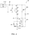
- FIG. 2 is a circuit diagram of a light-emitting module 20.
- the vehicle luminaire 1 can be provided with a socket 10, a light-emitting module 20, a power-supply unit 30, and a heat transfer portion 40.
- the socket 10 can include a mounting portion 11, a bayonet 12, a flange 13, and a radiating fin 14.
- the mounting portion 11 can be provided on a surface opposite to the installation side of the radiating fin 14 in the flange 13.
- the outer shape of the mounting portion 11 can be a pillar shape.
- the outer shape of the mounting portion 11 is, for example, a columnar shape.
- the mounting portion 11 can include a concave portion 11a opening to an end opposite to the flange 13.
- At least one slit 11b can be provided in the mounting portion 11.
- a corner portion of a substrate 21 can be provided in the slit 11b.
- the dimension (width) of the slit 11b in the circumferential direction of the mounting portion 11 can be slightly larger than the dimension of the corner portion of the substrate 21. With such a configuration, the substrate 21 can be positioned by inserting the corner portion of the substrate 21 into the slit 11b.
- the planar shape of the substrate 21 can be enlarged when the slit 11b is provided. Therefore, the number of elements mounted on the substrate 21 can be increased. Alternatively, since the outer dimension of the mounting portion 11 can be decreased, a decrease in size of the mounting portion 11 and further a decrease in size of the vehicle luminaire 1 can be realized.
- the bayonet 12 can be provided on the outer surface of the mounting portion 11. For example, the bayonet 12 protrudes toward the outside of the vehicle luminaire 1.
- the bayonet 12 can face the flange 13.
- a plurality of the bayonets 12 can be provided.
- the bayonet 12 can be used when mounting the vehicle luminaire 1 to a housing 101 of a vehicle lamp 100.
- the bayonet 12 can be used for a twist lock.
- the flange 13 can have a plate shape.
- the flange 13 can have a disk shape.
- the outer surface of the flange 13 can be located on the outside of the vehicle luminaire 1 in relation to the outer surface of the bayonet 12.
- the radiating fin 14 can be provided on the side opposite to the mounting portion 11 in the flange 13. At least one radiating fin 14 can be provided.
- the socket 10 illustrated in FIG. 1 is provided with a plurality of the radiating fins 14.
- the plurality of radiating fins 14 can be provided side by side in a predetermined direction.
- the radiating fin 14 can have a plate shape.
- the socket 10 can be provided with a hole 10a and a hole 10b.
- One end of the hole 10a opens to a bottom surface 11a1 of the concave portion 11a.
- a holder 32 can be provided inside the hole 10a.
- One end of the hole 10b is connected to the other end of the hole 10a.
- the other end of the hole 10b opens to an end on the side of the radiating fin 14 in the socket 10. End portions of a plurality of power-supply terminals 31 are exposed inside the hole 10b.
- a connector 105 having a seal member 105a is inserted into the hole 10b and the connector 105 is fitted to the ends of the plurality of power-supply terminals 31.
- the socket 10 can have a function of holding the light-emitting module 20 and the power-supply unit 30 and a function of transferring heat generated in the light-emitting module 20 to the outside. Therefore, it is preferable that the socket 10 be formed of a material having a high thermal conductivity such as metal.
- the socket 10 can efficiently radiate heat generated in the light-emitting module 20 and have light weight. Therefore, it is more preferable that the socket 10 be formed of a high thermal conductive resin.
- the high thermal conductive resin includes, for example, a resin and a filler using an inorganic material.
- the high thermal conductive resin can be obtained by mixing a filler using carbon or aluminum oxide with a resin such as polyethylene terephthalate (PET) or nylon.
- the socket 10 which is integrally formed with the mounting portion 11, the bayonet 12, the flange 13, and the radiating fin 14 by including a high thermal conductive resin, heat generated in the light-emitting module 20 can be efficiently radiated.
- the socket 10 can have a light weight.
- the mounting portion 11, the bayonet 12, the flange 13, and the radiating fin 14 can be integrally molded by using an injection-molding method or the like.
- the socket 10 and the power-supply unit 30 can be integrally molded by using an insert-molding method or the like.
- the power-supply unit 30 can include the plurality of power-supply terminals 31 and the holder 32.
- the plurality of power-supply terminals 31 can be pin-shaped bodies. The ends on the side of the light-emitting module 20 in the plurality of power-supply terminals 31 can be soldered to an output terminal 21a1 and an input terminal 21a2 of a wiring pattern 21a. The ends on the side of the radiating fin 14 in the plurality of power-supply terminals 31 are exposed inside the hole 10b.
- the power-supply terminal 31 can be formed of, for example, metal such as copper alloy. Additionally, the number, shape, arrangement, material, and the like of the power-supply terminals 31 are not limited to those illustrated above, but can be changed as appropriate.
- the socket 10 be formed of a material having high thermal conductivity.
- a material having high thermal conductivity may be conductive.
- a high thermal conductive resin or the like using carbon is conductive. Therefore, the holder 32 can be provided to insulate the power-supply terminal 31 and the conductive socket 10. Further, the holder 32 can also have a function of holding the plurality of power-supply terminals 31.
- the socket 10 is formed of a high thermal conductive resin having an insulation property (for example, a high thermal conductive resin or the like including aluminum oxide), the holder 32 can be omitted. In this case, the socket 10 can hold the plurality of power-supply terminals 31.
- the holder 32 can be formed of a material having an insulation property. For example, the holder 32 can be press-inserted into the hole 10a provided in the socket 10 or can be bonded to the inner wall of the hole 10a.
- the heat transfer portion 40 can be provided between the socket 10 and the light-emitting module 20 (the substrate 21).
- the heat transfer portion 40 can be provided to easily transfer heat generated in the light-emitting module 20 to the socket 10.
- the heat transfer portion 40 can include, for example, metal.
- the metal can be, for example, aluminum, aluminum alloy, copper, copper alloy, or the like.
- the heat transfer portion 40 can be bonded to the bottom surface 11a1 of the concave portion 11a.
- the adhesive can be an adhesive mixed with a filler using an inorganic material.
- the heat transfer portion 40 can also be attached to the bottom surface 11a1 of the concave portion 11a through a layer containing thermal conductive grease (thermal grease).
- the thermal conductive grease can be, for example, a mixture of modified silicone and a filler using an inorganic material. Further, the heat transfer portion 40 can be buried in the bottom surface 11a1 of the concave portion 11a by using an insert-molding method or the like.
- the heat transfer portion 40 can be omitted.
- the light-emitting module 20 can be bonded to the bottom surface 11a1 of the concave portion 11a.
- the light-emitting module 20 can be provided on one end side of the socket 10.
- the light-emitting module 20 can include the substrate 21, a light-emitting element 22, a diode 23, a first transistor 24, a negative characteristic thermistor 25, a positive characteristic thermistor 26, a second transistor 27, a frame portion 29a, and a sealing portion 29b. Further, the light-emitting module 20 can further include a resistor 25a, a resistor 25b, a resistor 26a (corresponding to an example of a second resistor), a resistor 27a, a resistor 27b, and a capacitor 28 to be described later. These elements can be electrically connected to the wiring pattern 21a provided in the substrate 21.
- the substrate 21 can be bonded to, for example, a surface 40a on the side opposite to the bottom surface 11a1 of the concave portion 11a in the heat transfer portion 40.
- the adhesive that bonds the substrate 21 to the heat transfer portion 40 can be the same as the adhesive that bonds the heat transfer portion 40 to the bottom surface 11a1 of the concave portion 11a.
- the substrate 21 can be formed of, for example, an inorganic material such as ceramics (for example, aluminum oxide or aluminum nitride) or an organic material such as paper phenol or glass epoxy. Further, the substrate 21 can be a metal plate of which a surface is coated with an insulating material.
- the substrate 21 be formed of a material having high thermal conductivity from the viewpoint of thermal radiation.
- the material having high thermal conductivity include ceramics such as aluminum oxide and aluminum nitride, a high thermal conductive resin, and a metal plate whose surface is coated with an insulating material.
- the substrate 21 may have a single-layer structure or a multi-layer structure.
- the wiring pattern 21a can be formed of, for example, a material containing silver as a main component or a material containing copper as a main component.
- the light-emitting element 22 can be provided on the side opposite to the heat transfer portion 40 in the substrate 21. At least one light-emitting element 22 can be provided. In the case of the vehicle luminaire 1 illustrated in FIGS. 1 and 2 , a plurality of the light-emitting elements 22 are provided. Additionally, when the plurality of light-emitting elements 22 are provided, the plurality of light-emitting elements 22 can be connected in series.
- the light-emitting element 22 can be, for example, a light-emitting diode, an organic light-emitting diode, a laser diode, or the like.
- the light-emitting element 22 can be, for example, a chip-shaped light-emitting element, a surface mount type light-emitting element, a shell type light-emitting element having a lead wire, or the like. However, the chip-shaped light-emitting element is preferable in consideration of a decrease in size of the light-emitting module 20 and further a decrease in size of the vehicle luminaire 1.
- the chip-shaped light-emitting element 22 can be mounted by chip on board (COB).
- the chip-shaped light-emitting element 22 can be, for example, a vertical light-emitting element, an upper light-emitting element, a flip chip light-emitting element, or the like.
- the light-emitting element 22 illustrated in FIG. 1 is the vertical light-emitting element.
- the diode 23 can be electrically connected across the light-emitting element 22 and the input terminal 21a2.
- the diode 23 can be provided to suppress a reverse voltage from being applied to the light-emitting element 22 and to suppress pulse noise from the reverse direction from being applied to the light-emitting element 22.
- the diode 23 can be, for example, a surface mount type diode or a diode having a lead wire.
- the diode 23 illustrated in FIG. 1 is a surface mount type diode.
- the first transistor 24 can be connected in series to the light-emitting element 22.
- the first transistor 24 can control the value of the current flowing through the light-emitting element 22 and further the total luminous flux of the light emitted from the light-emitting element 22.
- the first transistor 24 can be a field effect transistor (FET).
- FET field effect transistor
- the gate of the first transistor 24 can be electrically connected to the negative characteristic thermistor 25.
- the source of the first transistor 24 can be electrically connected to the cathode of the light-emitting element 22.
- the drain of the first transistor 24 can be electrically connected to the positive characteristic thermistor 26.
- the resistance value of the negative characteristic thermistor 25 gradually decreases when the temperature rises.
- the negative characteristic thermistor 25 be provided adjacent to the positive characteristic thermistor 26.
- the negative characteristic thermistor 25 since a difference between the temperature of the negative characteristic thermistor 25 and the temperature of the positive characteristic thermistor 26 can be minimized, an effect shown in FIGS. 5A to 5D to be described later can be effectively obtained.
- the negative characteristic thermistor 25 can be connected in series to the resistor 25a.
- the resistor 25a can be provided to suppress the resistance value of the portion where the negative characteristic thermistor 25 is provided from decreasing too much when the temperature of the negative characteristic thermistor 25 rises. That is, the resistor can be provided to suppress the negative characteristic thermistor 25 from being broken due to an overcurrent flowing through the negative characteristic thermistor 25 when the resistance value of the negative characteristic thermistor 25 becomes small.
- the resistor 25b connected in parallel to the negative characteristic thermistor 25 can be provided to adjust the change rate of the current I R flowing through the resistor 27a with respect to the temperature.
- the positive characteristic thermistor 26 can be connected in series to the light-emitting element 22 via the first transistor 24.
- the light-emitting element 22 and the positive characteristic thermistor 26 are thermally connected to each other through the substrate 21 or the wiring pattern 21a. Therefore, when the temperature of the light-emitting element 22 rises, the temperature of the positive characteristic thermistor 26 rises and the resistance value of the positive characteristic thermistor 26 rises. Since the value of the current flowing through the light-emitting element 22 decreases when the resistance value of the positive characteristic thermistor 26 increases, an increase in the temperature of the light-emitting element 22 can be suppressed. Therefore, it is possible to suppress the light-emitting element 22 from being broken or to suppress the life of the light-emitting element 22 from being shortened.
- the resistor 26a connected in parallel to the positive characteristic thermistor 26 can be provided to reduce an influence due to a variation in the resistance value of the positive characteristic thermistor 26.
- the second transistor 27 can be, for example, a bipolar transistor.
- the collector of the second transistor 27 can be electrically connected to the gate of the first transistor 24 and the negative characteristic thermistor 25.
- the base of the second transistor 27 can be electrically connected to the drain of the first transistor 24 and the positive characteristic thermistor 26.
- the emitter of the second transistor 27 can be electrically connected to the output terminal 21a1 via the resistor 27a.
- the resistor 27a can be provided to increase the sum of a voltage V BE across the base and the emitter of the second transistor 27 and a voltage V 27a across both ends of the resistor 27a.
- the resistor 27b can be provided to ensure the voltage for operating the gate of the first transistor 24. Further, the resistance value of the resistor 27b is set to be higher than a threshold voltage at which the gate is operated by the voltage division of the combined resistance of the resistor 25a, the resistor 25b, and the negative characteristic thermistor 25.
- the capacitor 28 can be provided, for example, as a measure against noise and smoothing the voltage.
- the frame portion 29a can be bonded to the substrate 21.
- the frame portion 29a can have a frame shape.
- At least one light-emitting element 22 can be provided in a region surrounded by the frame portion 29a.
- the frame portion 29a can surround the plurality of light-emitting elements 22.
- the frame portion 29a is molded by an injection-molding method or the like and the molded frame portion 29a is bonded to the substrate 21 has been illustrated, but the invention is not limited thereto.
- the frame portion 29a can also be formed, for example, by applying a melted resin in a frame shape on the substrate 21 using a dispenser or the like and curing the resin.
- the frame portion 29a can have a function of a reflector that reflects the light emitted from the light-emitting element 22.
- the frame portion 29a can be omitted.
- a dome-shaped sealing portion 29b is formed on the substrate 21.
- the formation range of the sealing portion 29b can be defined when the frame portion 29a is provided. Therefore, since an increase in the planar dimension of the sealing portion 29b can be suppressed, a decrease in size of the substrate 21 and further a decrease in size of the vehicle luminaire 1 can be realized.
- the sealing portion 29b can be provided inside the frame portion 29a.
- the sealing portion 29b can cover a region surrounded by the frame portion 29a.
- the sealing portion 29b can cover the light-emitting element 22.
- the sealing portion 29b can be formed of a light transmitting material.
- the sealing portion 29b can be formed by filling, for example, a resin into the region surrounded by the frame portion 29a.
- the resin can be filled by using, for example, a dispenser or the like.
- the resin to be filled can be, for example, a silicone resin or the like.
- the sealing portion 29b can include a phosphor.
- the phosphor can be, for example, a YAG-based phosphor (yttrium-aluminum-garnet-based phosphor). However, the type of phosphor can be appropriately changed so as to obtain a predetermined emission color according to the application of the vehicle luminaire 1.
- the frame portion 29a and the sealing portion 29b can be omitted.
- the light-emitting element 22 is a chip-shaped light-emitting element and the frame portion 29a and the sealing portion 29b are provided when a decrease in size of the substrate 21 is considered.
- FIG. 3 is a circuit diagram of the light-emitting module 120 according to the comparative example.
- the light-emitting module 120 according to the comparative example is not provided with the negative characteristic thermistor 25 and the positive characteristic thermistor 26.
- the voltage V BE is about 0.63 V.
- the voltage V BE is about 0.46 V.
- the resistance value of the resistor 26a is 2 ⁇
- the current I F when the temperature of the second transistor 27 is 25°C is about 0.315 A.
- the current I F when the temperature of the second transistor 27 is 100°C is about 0.23 A.
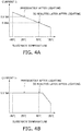
- FIG. 4A is a graph showing a relationship between the current I F and the substrate temperature in the light-emitting module 120.
- FIG. 4B is a graph showing a desired relationship between the current I F and the substrate temperature in the vehicle luminaire 1.
- the temperature of the substrate 21 gradually rises due to the heat generated when lighting the light-emitting element 22. Since the temperature of the second transistor 27 gradually rises when the temperature of the substrate 21 gradually rises, the current I F flowing through the light-emitting element 22 gradually decreases as shown in FIG. 4A . Therefore, the total luminous flux of the light emitted from the vehicle luminaire may decrease over time and the driver may feel uncomfortable.
- the temperature of the light-emitting element 22 is too high, there is a risk that the light-emitting element 22 may be broken or the life may be shortened. Therefore, when the temperature of the substrate 21 is too high (the temperature of the light-emitting element 22 is too high), it is preferable to suppress the temperature of the light-emitting element 22 from increasing too high by reducing the current I F flowing through the light-emitting element 22 as shown in FIG. 4B .
- a decrease in the total luminous flux is reduced by providing the negative characteristic thermistor 25. Further, the temperature of the light-emitting element 22 is suppressed from increasing too high by providing the positive characteristic thermistor 26.
- FIGS. 5A to 5D are graphs showing the operation of the negative characteristic thermistor 25.
- the resistance value of the negative characteristic thermistor 25 corresponding to the negative characteristic thermistor gradually decreases in accordance with an increase in the temperature. Therefore, as shown in FIG. 5A , the combined resistance value R1 of the negative characteristic thermistor 25 and the resistor 25a gradually decreases as the lighting time elapses. Additionally, since the resistance value of the resistor 25a is substantially constant even when the temperature rises, a decrease in the combined resistance value R1 can be limited.
- the current I R flowing through the resistor 27a increases in accordance with a decrease in the combined resistance value R1. Additionally, since a decrease in the combined resistance value R1 is limited as described above, an increase in the current I R can also be limited.
- the total luminous flux can be suppressed from decreasing with the elapse of the lighting time.
- FIGS. 6A to 6D are graphs showing the operation of the positive characteristic thermistor 26.
- the junction temperature T j of the light-emitting element 22 may exceed the rated value as shown in FIG. 6A .
- the junction temperature T j exceeds the rated value, there is a risk that the light-emitting element 22 may be broken or the life may be shortened.
- the resistance value rapidly increases.
- the combined resistance value R2 of the positive characteristic thermistor 26 and the resistor 26a also rapidly increases when the temperature exceeds the Curie point.
- the current I F flowing through the light-emitting element 22 can be rapidly reduced when the temperature of the light-emitting element 22 becomes too high as shown in FIG. 6C . Therefore, as shown in FIG. 6D , it is possible to suppress the junction temperature T j of the light-emitting element 22 from exceeding the rated value.
- the positive characteristic thermistor 26 when the positive characteristic thermistor 26 is provided, it is possible to suppress the temperature of the light-emitting element 22 from becoming too high. Therefore, it is possible to suppress the light-emitting element 22 from being broken or to suppress the life from being shortened.
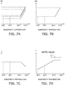
- FIGS. 7A to 7D are graphs showing the operation of the resistor 26a.
- the resistance value of the positive characteristic thermistor 26 has a variation of about ⁇ 20%. Therefore, when the resistance value of the resistor 26a is constant, the combined resistance value R2 of the positive characteristic thermistor 26 and the resistor 26a also varies as shown in FIG. 7A . When the combined resistance value R2 varies, the total luminous flux of the light emitted from the light-emitting element 22 varies. Further, there is a risk that the junction temperature T j of the light-emitting element 22 may exceed the rated value.
- the resistance value of the resistor 26a can be changed in response to the resistance value of the positive characteristic thermistor 26 so that the combined resistance value R2 falls within a predetermined range.
- the combined resistance value R2 When the combined resistance value R2 is within a predetermined range, a variation in the current I F flowing through the light-emitting element 22 can be suppressed as shown in FIG. 7C . As a result, a variation in the total luminous flux of the light emitted from the light-emitting element 22 can be suppressed. Further, as shown in FIG. 7D , the junction temperature T j of the light-emitting element 22 can be suppressed from exceeding the rated value.
- the resistor 26a can be, for example, a variable resistor. Further, the resistance value can be increased by configuring the resistor 26a as a film-shaped resistor and cutting off a part of the film-shaped resistor.
- the film-shaped resistor can include, for example, ruthenium oxide or the like. A part of the resistor can be cut off by irradiating the film-shaped resistor with laser. That is, the resistor 26a can have a film shape and include a slit 26a1.
- a resistor having an appropriate resistance value may be selected in response to the resistance value of the positive characteristic thermistor 26.
- the resistor can be a surface mount type resistor or a resistor having a lead wire.
- the resistor 26a may be connected in parallel to the positive characteristic thermistor 26 and change the resistance value in response to a variation in the resistance value of the positive characteristic thermistor 26 at a normal temperature (for example, 25°C).
- the light-emitting element 22 can be protected and a variation in the total luminous flux in accordance with a change in temperature can be suppressed.
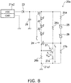
- FIG. 8 is a circuit diagram illustrating a light-emitting module 20a provided in a vehicle luminaire 1a according to another embodiment.
- FIGS. 9A to 9D are graphs showing the operations and effects of the positive characteristic thermistor 26 and the negative characteristic thermistor 25 connected in series to each other.
- the light-emitting module 20a can include the substrate 21, the light-emitting element 22, the diode 23, the first transistor 24, the negative characteristic thermistor 25, the positive characteristic thermistor 26, the second transistor 27, the frame portion 29a, and the sealing portion 29b. Further, the light-emitting module 20 can further include a resistor 25a, a resistor 25b, a resistor 26b, a resistor 27a, a resistor 27b, and a capacitor 28. These elements can be electrically connected to the wiring pattern 21a provided in the substrate 21.
- the positive characteristic thermistor 26 is connected in parallel to the resistor 26a.
- the positive characteristic thermistor 26 is connected in series to the negative characteristic thermistor 25.
- the negative characteristic thermistor 25 may be electrically connected to the input terminal 21a2 and the positive characteristic thermistor 26 may be electrically connected to the input terminal 21a2.
- the collector of the second transistor 27 is electrically connected to the gate of the first transistor 24 and the negative characteristic thermistor 25 or the positive characteristic thermistor 26.
- the base of the second transistor 27 is electrically connected to the drain of the first transistor 24.
- the emitter of the second transistor 27 is electrically connected to the output terminal 21a1.
- the resistance value of the negative characteristic thermistor 25 gradually decreases in accordance with an increase in the temperature.
- the resistance value of the positive characteristic thermistor 26 abruptly increases when the temperature exceeds the Curie point. Therefore, as shown in FIG. 9A , the combined resistance value R3 of the negative characteristic thermistor 25, the positive characteristic thermistor 26, and the resistor 25a gradually decreases in accordance with a decrease in the resistance value of the negative characteristic thermistor 25 when the temperature of the substrate 21 is relatively low. Additionally, since the light-emitting module 20a is also provided with the resistor 25a, a decrease in the combined resistance value R3 can also be limited. On the other hand, when the temperature of the positive characteristic thermistor 26 exceeds the Curie point, the combined resistance value R3 rapidly increases in accordance with a rapid increase in the resistance value of the positive characteristic thermistor 26.
- the current I R flowing through the resistor 27a changes in response to a change in the combined resistance value R3. Additionally, since a decrease in the combined resistance value R3 is limited, an increase in the current I R can also be limited.
- the resistance value of the resistor 25a can be, for example, about 2.2 kQ.
- the resistance value of the resistor 25a is substantially constant even when the temperature rises.
- the resistance value of the negative characteristic thermistor 25 becomes much larger than the resistance value of the positive characteristic thermistor 26.
- the resistance value of the negative characteristic thermistor 25 is about 10 k ⁇ and the resistance value of the positive characteristic thermistor 26 is about 470 ⁇ . Since the resistance value of the resistor 25a and the resistance value of the negative characteristic thermistor 25 are larger than the resistance value of the positive characteristic thermistor 26, a variation in the combined resistance value R3 is extremely small even when the resistance value of the positive characteristic thermistor 26 varies. For example, even when a variation in the resistance value of the positive characteristic thermistor 26 is about ⁇ 50%, a variation in the combined resistance value R3 can be about ⁇ 2%.
- the resistance value of the positive characteristic thermistor 26 is much larger than the resistance value of the negative characteristic thermistor 25.
- the combined resistance value R3 also varies largely.
- the resistance value of the resistor 25a is large, the influence can be reduced.
- the current I F flowing through the light-emitting element 22 be rapidly reduced in order to protect the light-emitting element 22. Therefore, since the combined resistance value R3 varies, there is no problem even when a variation in the current I F and further a variation in the total luminous flux become large.
- the light-emitting element 22 can be protected and a variation in the total luminous flux in accordance with a change in the temperature can be suppressed. Further, the above-described resistor 26a can be also omitted.
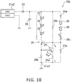
- FIG. 10 is a circuit diagram illustrating a light-emitting module 20b provided in a vehicle luminaire 1b according to another embodiment.
- FIGS. 11A to 11D are graphs showing the operation and effect of a resistor 26c (corresponding to an example of a first resistor) connected in series to the positive characteristic thermistor 26.
- the light-emitting module 20b is a case in which the resistor 26c is further provided in the light-emitting module 20a.
- the resistor 26c can be connected in series to the positive characteristic thermistor 26.
- an influence due to a variation in the resistance value of the positive characteristic thermistor 26 can be reduced.
- the combined resistance value R3, the current I R flowing through the resistor 27a, and the junction temperature T j of the light-emitting element 22 may vary, for example, by about 2% as shown in FIGS. 9A to 9D .
- the combined resistance value can be within a predetermined range.
- a variation in the combined resistance value R4 of the negative characteristic thermistor 25, the positive characteristic thermistor 26, the resistor 25a, and the resistor 26c can be reduced.
- a variation in the current I R flowing through the resistor 27a can be reduced.
- a variation in the current I F flowing through the light-emitting element 22 can be reduced.
- a variation in the junction temperature T j of the light-emitting element 22 can be reduced.
- the resistor 26c can be connected in series to the positive characteristic thermistor 26 and the resistance value can be changed in response to a variation in the resistance value of the positive characteristic thermistor 26 at a normal temperature (for example, 25°C).
- the resistor 26c can be similar to, for example, the above-described resistor 26a.
- the resistor 26c can have a film shape and have a slit. Further, the resistor 26c can include ruthenium oxide similarly to the above-described resistor 26a.
- the positive characteristic thermistor 26 can be electrically connected to the gate of the first transistor 24 or the drain of the first transistor 24.
- the collector can be electrically connected to the gate of the first transistor 24, the base can be electrically connected to the drain of the first transistor 24, and the emitter can be electrically connected to the output terminal.
- the positive characteristic thermistor 26 when the positive characteristic thermistor 26 is electrically connected to the gate of the first transistor 24, the positive characteristic thermistor 26 and the negative characteristic thermistor 25 may be connected in series to each other as shown in FIG. 8 .
- the base of the second transistor 27 can be electrically connected to the drain of the first transistor 24 and the positive characteristic thermistor 26 as shown in FIG. 2 .
- the vehicle lamp 100 is a front combination light provided in an automobile
- the vehicle lamp 100 is not limited to a front combination light provided in an automobile.
- the vehicle lamp 100 may be a vehicle lamp provided in an automobile or a rail car.
- FIG. 12 is a schematic partially cross-sectional view illustrating the vehicle lamp 100.
- the vehicle lamp 100 can be provided with the vehicle luminaire 1 (1a, 1b), the housing 101, a cover 102, an optical element 103, a seal member 104, and the connector 105.
- the vehicle luminaire 1 (1a, 1b) can be attached to the housing 101.
- the housing 101 can hold the mounting portion 11.
- the housing 101 can have a box shape whose one end side is opened.
- the housing 101 can be formed of, for example, a resin or the like through which light is not transmitted.
- a bottom surface of the housing 101 can be provided with an attachment hole 101a into which a portion provided with the bayonet 12 in the mounting portion 11 is inserted.
- a circumferential edge of the attachment hole 101a can be provided with a concave portion into which the bayonet 12 provided in the mounting portion 11 is inserted. Additionally, a case in which the attachment hole 101a is directly provided in the housing 101 has been illustrated, but an attachment member having the attachment hole 101a may be provided in the housing 101.
- the cover 102 can be provided to block the opening of the housing 101.
- the cover 102 can be formed of a resin having translucency.
- the cover 102 can have a function of a lens or the like.
- the optical element 103 can perform reflection, diffusion, light guiding, light collection, formation of a predetermined light distribution pattern, and the like of the light emitted from the vehicle luminaire 1 (1a, 1b).
- the optical element 103 illustrated in FIG. 12 is a reflector. In this case, the optical element 103 can form a predetermined light distribution pattern by reflecting the light emitted from the vehicle luminaire 1 (1a, 1b).
- the seal member 104 can be provided between the flange 13 and the housing 101.
- the seal member 104 can have an annular shape.
- the seal member 104 can be formed of an elastic material such as rubber or silicone resin.
- the seal member 104 When the vehicle luminaire 1 (1a, 1b) is attached to the vehicle lamp 100, the seal member 104 is sandwiched between the flange 13 and the housing 101. Therefore, the internal space of the housing 101 can be sealed by the seal member 104. Further, the bayonet 12 is pressed against the housing 101 by the elastic force of the seal member 104. Therefore, the separation of the vehicle luminaire 1 (1a, 1b) from the housing 101 can be suppressed.
- the connector 105 can be fitted to the ends of the plurality of power-supply terminals 31 exposed inside the hole 10b.
- a power-supply (not shown) or the like can be eclectically connected to the connector 105. Therefore, a power-supply (not shown) or the like can be electrically connected to the light-emitting element 22 by fitting the connector 105 to the ends of the plurality of power-supply terminals 31.
- the connector 105 can be provided with the seal member 105a.
- the seal member 105a has an annular shape and can be formed of an elastic material such as rubber or silicone resin.
Landscapes
- Engineering & Computer Science (AREA)
- General Engineering & Computer Science (AREA)
- Microelectronics & Electronic Packaging (AREA)
- Ceramic Engineering (AREA)
- Physics & Mathematics (AREA)
- Electromagnetism (AREA)
- Non-Portable Lighting Devices Or Systems Thereof (AREA)
- Lighting Device Outwards From Vehicle And Optical Signal (AREA)
- Fastening Of Light Sources Or Lamp Holders (AREA)
- Arrangement Of Elements, Cooling, Sealing, Or The Like Of Lighting Devices (AREA)
- Circuit Arrangement For Electric Light Sources In General (AREA)
Abstract
Description
- Embodiments described herein relate to a vehicle luminaire and a vehicle lamp.
- From the viewpoint of energy saving and long life, a vehicle luminaire having a light-emitting diode has been widely used instead of a vehicle luminaire having a filament.
- When lighting the vehicle luminaire, a voltage is applied to the vehicle luminaire (the light-emitting diode). When a voltage is applied to the light-emitting diode, a current flows through the light-emitting diode so that heat is generated and the temperature of the light-emitting diode rises. Further, in the case of the vehicle luminaire for an automobile, a high voltage may be applied to the light-emitting diode due to a variation in input voltage or an environmental temperature may become high in some cases. In this case, when the temperature of the light-emitting diode is too high, there is a risk that the light-emitting diode may be broken or the life of the light-emitting diode may be shortened.
- Here, when the temperature of the light-emitting diode is too high due to a parallel connection of a resistor and a circuit in which a resistor and a positive characteristic thermistor are connected in series to each other, there is proposed a technique in which a current flows only to the resistor connected in parallel by interrupting a current flowing to the circuit by the positive characteristic thermistor. With such a configuration, the light-emitting diode can be protected. However, there was a room for improvement in suppressing a variation in total luminous flux with a change in temperature.
- Here, it has been desired to develop a technique capable of protecting a light-emitting diode and suppressing a variation in total luminous flux with a change in temperature.
-
-
FIG. 1 is a schematic exploded view of a vehicle luminaire according to an embodiment. -
FIG. 2 is a circuit diagram of a light-emitting module. -
FIG. 3 is a circuit diagram of a light-emitting module according to a comparative example. -
FIG. 4A is a graph showing a relationship between a current and a substrate temperature in the light-emitting module andFIG. 4B is a graph showing a desired relationship between a current and a substrate temperature in the vehicle luminaire. -
FIGS. 5A to 5D are graphs showing the operation of a negative characteristic thermistor. -
FIGS. 6A to 6D are graphs showing the operation of a positive characteristic thermistor. -
FIGS. 7A to 7D are graphs showing the operation of a resistor. -
FIG. 8 is a circuit diagram illustrating a light-emitting module provided in a vehicle luminaire according to another embodiment. -
FIGS. 9A to 9D are graphs showing operations and effects of a positive characteristic thermistor and a negative characteristic thermistor connected in series to each other. -
FIG. 10 is a circuit diagram illustrating a light-emitting module according to another embodiment. -
FIGS. 11A to 11D are graphs showing operations and effects of a resistor connected in series to a positive characteristic thermistor. -
FIG. 12 is a schematic partially cross-sectional view illustrating a vehicle lamp. - A vehicle luminaire according to an embodiment includes: a socket; and a light-emitting module which is provided at one end side of the socket. The light-emitting module includes: at least one light-emitting element; a first transistor of which a source is electrically connected to a cathode of the light-emitting element; a negative characteristic thermistor which is electrically connected to a gate of the first transistor; a positive characteristic thermistor which is electrically connected to the gate of the first transistor or a drain of the first transistor; and a second transistor of which a collector is electrically connected to the gate of the first transistor, a base is electrically connected to the drain of the first transistor, and an emitter is electrically connected to an output terminal.
- Hereinafter, an embodiment will be illustrated with reference to the drawings. In the drawings, the same components are indicated by the same reference numerals and detailed description thereof will be appropriately omitted.
- A
vehicle luminaire 1 according to an embodiment can be provided in, for example, automobiles and rail cars. Examples of thevehicle luminaire 1 provided in automobiles include, for example, a front combination light (for example, an appropriate combination of a daytime running lamp (DRL), a position lamp, a turn signal lamp, and the like), a rear combination light (for example, an appropriate combination of a stop lamp, a tail lamp, a turn signal lamp, a back lamp, a fog lamp, and the like), and the like. However, the application of thevehicle luminaire 1 is not limited to these. -
FIG. 1 is a schematic exploded view of thevehicle luminaire 1 according to the embodiment. -
FIG. 2 is a circuit diagram of a light-emitting module 20. - As shown in
FIG. 1 , thevehicle luminaire 1 can be provided with asocket 10, a light-emitting module 20, a power-supply unit 30, and aheat transfer portion 40. - The
socket 10 can include amounting portion 11, abayonet 12, aflange 13, and a radiatingfin 14. - The
mounting portion 11 can be provided on a surface opposite to the installation side of the radiatingfin 14 in theflange 13. The outer shape of themounting portion 11 can be a pillar shape. The outer shape of themounting portion 11 is, for example, a columnar shape. Themounting portion 11 can include aconcave portion 11a opening to an end opposite to theflange 13. - At least one
slit 11b can be provided in themounting portion 11. A corner portion of asubstrate 21 can be provided in theslit 11b. The dimension (width) of theslit 11b in the circumferential direction of themounting portion 11 can be slightly larger than the dimension of the corner portion of thesubstrate 21. With such a configuration, thesubstrate 21 can be positioned by inserting the corner portion of thesubstrate 21 into theslit 11b. - Further, the planar shape of the
substrate 21 can be enlarged when theslit 11b is provided. Therefore, the number of elements mounted on thesubstrate 21 can be increased. Alternatively, since the outer dimension of themounting portion 11 can be decreased, a decrease in size of themounting portion 11 and further a decrease in size of thevehicle luminaire 1 can be realized. - The
bayonet 12 can be provided on the outer surface of themounting portion 11. For example, thebayonet 12 protrudes toward the outside of thevehicle luminaire 1. Thebayonet 12 can face theflange 13. A plurality of thebayonets 12 can be provided. Thebayonet 12 can be used when mounting thevehicle luminaire 1 to ahousing 101 of avehicle lamp 100. Thebayonet 12 can be used for a twist lock. - The
flange 13 can have a plate shape. For example, theflange 13 can have a disk shape. The outer surface of theflange 13 can be located on the outside of thevehicle luminaire 1 in relation to the outer surface of thebayonet 12. - The radiating
fin 14 can be provided on the side opposite to the mountingportion 11 in theflange 13. At least one radiatingfin 14 can be provided. For example, thesocket 10 illustrated inFIG. 1 is provided with a plurality of the radiatingfins 14. The plurality of radiatingfins 14 can be provided side by side in a predetermined direction. The radiatingfin 14 can have a plate shape. - Further, the
socket 10 can be provided with ahole 10a and ahole 10b. One end of thehole 10a opens to a bottom surface 11a1 of theconcave portion 11a. Aholder 32 can be provided inside thehole 10a. One end of thehole 10b is connected to the other end of thehole 10a. The other end of thehole 10b opens to an end on the side of the radiatingfin 14 in thesocket 10. End portions of a plurality of power-supply terminals 31 are exposed inside thehole 10b. Aconnector 105 having aseal member 105a is inserted into thehole 10b and theconnector 105 is fitted to the ends of the plurality of power-supply terminals 31. - The
socket 10 can have a function of holding the light-emittingmodule 20 and the power-supply unit 30 and a function of transferring heat generated in the light-emittingmodule 20 to the outside. Therefore, it is preferable that thesocket 10 be formed of a material having a high thermal conductivity such as metal. - Further, in recent years, it is preferable that the
socket 10 can efficiently radiate heat generated in the light-emittingmodule 20 and have light weight. Therefore, it is more preferable that thesocket 10 be formed of a high thermal conductive resin. The high thermal conductive resin includes, for example, a resin and a filler using an inorganic material. For example, the high thermal conductive resin can be obtained by mixing a filler using carbon or aluminum oxide with a resin such as polyethylene terephthalate (PET) or nylon. - According to the
socket 10 which is integrally formed with the mountingportion 11, thebayonet 12, theflange 13, and the radiatingfin 14 by including a high thermal conductive resin, heat generated in the light-emittingmodule 20 can be efficiently radiated. Further, thesocket 10 can have a light weight. In this case, the mountingportion 11, thebayonet 12, theflange 13, and the radiatingfin 14 can be integrally molded by using an injection-molding method or the like. Further, thesocket 10 and the power-supply unit 30 can be integrally molded by using an insert-molding method or the like. - The power-
supply unit 30 can include the plurality of power-supply terminals 31 and theholder 32. - The plurality of power-
supply terminals 31 can be pin-shaped bodies. The ends on the side of the light-emittingmodule 20 in the plurality of power-supply terminals 31 can be soldered to an output terminal 21a1 and an input terminal 21a2 of awiring pattern 21a. The ends on the side of the radiatingfin 14 in the plurality of power-supply terminals 31 are exposed inside thehole 10b. The power-supply terminal 31 can be formed of, for example, metal such as copper alloy. Additionally, the number, shape, arrangement, material, and the like of the power-supply terminals 31 are not limited to those illustrated above, but can be changed as appropriate. - As described above, it is preferable that the
socket 10 be formed of a material having high thermal conductivity. Incidentally, a material having high thermal conductivity may be conductive. For example, a high thermal conductive resin or the like using carbon is conductive. Therefore, theholder 32 can be provided to insulate the power-supply terminal 31 and theconductive socket 10. Further, theholder 32 can also have a function of holding the plurality of power-supply terminals 31. Additionally, when thesocket 10 is formed of a high thermal conductive resin having an insulation property (for example, a high thermal conductive resin or the like including aluminum oxide), theholder 32 can be omitted. In this case, thesocket 10 can hold the plurality of power-supply terminals 31. Theholder 32 can be formed of a material having an insulation property. For example, theholder 32 can be press-inserted into thehole 10a provided in thesocket 10 or can be bonded to the inner wall of thehole 10a. - The
heat transfer portion 40 can be provided between thesocket 10 and the light-emitting module 20 (the substrate 21). Theheat transfer portion 40 can be provided to easily transfer heat generated in the light-emittingmodule 20 to thesocket 10. Theheat transfer portion 40 can include, for example, metal. The metal can be, for example, aluminum, aluminum alloy, copper, copper alloy, or the like. Theheat transfer portion 40 can be bonded to the bottom surface 11a1 of theconcave portion 11a. In this case, it is preferable that the adhesive have high thermal conductivity. For example, the adhesive can be an adhesive mixed with a filler using an inorganic material. Further, theheat transfer portion 40 can also be attached to the bottom surface 11a1 of theconcave portion 11a through a layer containing thermal conductive grease (thermal grease). The thermal conductive grease can be, for example, a mixture of modified silicone and a filler using an inorganic material. Further, theheat transfer portion 40 can be buried in the bottom surface 11a1 of theconcave portion 11a by using an insert-molding method or the like. - Additionally, when the heat generated in the light-emitting
module 20 is small, theheat transfer portion 40 can be omitted. When theheat transfer portion 40 is omitted, for example, the light-emittingmodule 20 can be bonded to the bottom surface 11a1 of theconcave portion 11a. - The light-emitting
module 20 can be provided on one end side of thesocket 10. - The light-emitting
module 20 can include thesubstrate 21, a light-emittingelement 22, adiode 23, afirst transistor 24, a negativecharacteristic thermistor 25, a positivecharacteristic thermistor 26, asecond transistor 27, aframe portion 29a, and a sealingportion 29b. Further, the light-emittingmodule 20 can further include aresistor 25a, aresistor 25b, aresistor 26a (corresponding to an example of a second resistor), aresistor 27a, aresistor 27b, and acapacitor 28 to be described later. These elements can be electrically connected to thewiring pattern 21a provided in thesubstrate 21. - The
substrate 21 can be bonded to, for example, asurface 40a on the side opposite to the bottom surface 11a1 of theconcave portion 11a in theheat transfer portion 40. The adhesive that bonds thesubstrate 21 to theheat transfer portion 40 can be the same as the adhesive that bonds theheat transfer portion 40 to the bottom surface 11a1 of theconcave portion 11a. Thesubstrate 21 can be formed of, for example, an inorganic material such as ceramics (for example, aluminum oxide or aluminum nitride) or an organic material such as paper phenol or glass epoxy. Further, thesubstrate 21 can be a metal plate of which a surface is coated with an insulating material. When the light-emittingelement 22 generates a large amount of heat, it is preferable that thesubstrate 21 be formed of a material having high thermal conductivity from the viewpoint of thermal radiation. Examples of the material having high thermal conductivity include ceramics such as aluminum oxide and aluminum nitride, a high thermal conductive resin, and a metal plate whose surface is coated with an insulating material. Further, thesubstrate 21 may have a single-layer structure or a multi-layer structure. - Further, a surface of the
substrate 21 can be provided with thewiring pattern 21a. Thewiring pattern 21a can be formed of, for example, a material containing silver as a main component or a material containing copper as a main component. - The light-emitting
element 22 can be provided on the side opposite to theheat transfer portion 40 in thesubstrate 21. At least one light-emittingelement 22 can be provided. In the case of thevehicle luminaire 1 illustrated inFIGS. 1 and2 , a plurality of the light-emittingelements 22 are provided. Additionally, when the plurality of light-emittingelements 22 are provided, the plurality of light-emittingelements 22 can be connected in series. - The light-emitting
element 22 can be, for example, a light-emitting diode, an organic light-emitting diode, a laser diode, or the like. - The light-emitting
element 22 can be, for example, a chip-shaped light-emitting element, a surface mount type light-emitting element, a shell type light-emitting element having a lead wire, or the like. However, the chip-shaped light-emitting element is preferable in consideration of a decrease in size of the light-emittingmodule 20 and further a decrease in size of thevehicle luminaire 1. The chip-shaped light-emittingelement 22 can be mounted by chip on board (COB). The chip-shaped light-emittingelement 22 can be, for example, a vertical light-emitting element, an upper light-emitting element, a flip chip light-emitting element, or the like. The light-emittingelement 22 illustrated inFIG. 1 is the vertical light-emitting element. - As shown in
FIG. 2 , thediode 23 can be electrically connected across the light-emittingelement 22 and the input terminal 21a2. Thediode 23 can be provided to suppress a reverse voltage from being applied to the light-emittingelement 22 and to suppress pulse noise from the reverse direction from being applied to the light-emittingelement 22. Thediode 23 can be, for example, a surface mount type diode or a diode having a lead wire. Thediode 23 illustrated inFIG. 1 is a surface mount type diode. - The
first transistor 24 can be connected in series to the light-emittingelement 22. Thefirst transistor 24 can control the value of the current flowing through the light-emittingelement 22 and further the total luminous flux of the light emitted from the light-emittingelement 22. Thefirst transistor 24 can be a field effect transistor (FET). The gate of thefirst transistor 24 can be electrically connected to the negativecharacteristic thermistor 25. The source of thefirst transistor 24 can be electrically connected to the cathode of the light-emittingelement 22. The drain of thefirst transistor 24 can be electrically connected to the positivecharacteristic thermistor 26. - The resistance value of the negative
characteristic thermistor 25 gradually decreases when the temperature rises. - As shown in
FIG. 1 , it is preferable that the negativecharacteristic thermistor 25 be provided adjacent to the positivecharacteristic thermistor 26. With such a configuration, since a difference between the temperature of the negativecharacteristic thermistor 25 and the temperature of the positivecharacteristic thermistor 26 can be minimized, an effect shown inFIGS. 5A to 5D to be described later can be effectively obtained. - The negative
characteristic thermistor 25 can be connected in series to theresistor 25a. Theresistor 25a can be provided to suppress the resistance value of the portion where the negativecharacteristic thermistor 25 is provided from decreasing too much when the temperature of the negativecharacteristic thermistor 25 rises. That is, the resistor can be provided to suppress the negativecharacteristic thermistor 25 from being broken due to an overcurrent flowing through the negativecharacteristic thermistor 25 when the resistance value of the negativecharacteristic thermistor 25 becomes small. - Additionally, the
resistor 25b connected in parallel to the negativecharacteristic thermistor 25 can be provided to adjust the change rate of the current IR flowing through theresistor 27a with respect to the temperature. - When the temperature of the positive
characteristic thermistor 26 exceeds the Curie point, the resistance value rapidly increases. The positivecharacteristic thermistor 26 can be connected in series to the light-emittingelement 22 via thefirst transistor 24. The light-emittingelement 22 and the positivecharacteristic thermistor 26 are thermally connected to each other through thesubstrate 21 or thewiring pattern 21a. Therefore, when the temperature of the light-emittingelement 22 rises, the temperature of the positivecharacteristic thermistor 26 rises and the resistance value of the positivecharacteristic thermistor 26 rises. Since the value of the current flowing through the light-emittingelement 22 decreases when the resistance value of the positivecharacteristic thermistor 26 increases, an increase in the temperature of the light-emittingelement 22 can be suppressed. Therefore, it is possible to suppress the light-emittingelement 22 from being broken or to suppress the life of the light-emittingelement 22 from being shortened. - Additionally, the
resistor 26a connected in parallel to the positivecharacteristic thermistor 26 can be provided to reduce an influence due to a variation in the resistance value of the positivecharacteristic thermistor 26. - The operations and effects of the negative
characteristic thermistor 25, the positivecharacteristic thermistor 26, and theresistor 26a will be described in detail later (for example, seeFIGS. 4A to 7D ). - The
second transistor 27 can be, for example, a bipolar transistor. The collector of thesecond transistor 27 can be electrically connected to the gate of thefirst transistor 24 and the negativecharacteristic thermistor 25. The base of thesecond transistor 27 can be electrically connected to the drain of thefirst transistor 24 and the positivecharacteristic thermistor 26. The emitter of thesecond transistor 27 can be electrically connected to the output terminal 21a1 via theresistor 27a. - For example, the
resistor 27a can be provided to increase the sum of a voltage VBE across the base and the emitter of thesecond transistor 27 and a voltage V27a across both ends of theresistor 27a. - Additionally, the
resistor 27b can be provided to ensure the voltage for operating the gate of thefirst transistor 24. Further, the resistance value of theresistor 27b is set to be higher than a threshold voltage at which the gate is operated by the voltage division of the combined resistance of theresistor 25a, theresistor 25b, and the negativecharacteristic thermistor 25. - Further, the
capacitor 28 can be provided, for example, as a measure against noise and smoothing the voltage. - As shown in
FIG. 1 , theframe portion 29a can be bonded to thesubstrate 21. Theframe portion 29a can have a frame shape. At least one light-emittingelement 22 can be provided in a region surrounded by theframe portion 29a. For example, theframe portion 29a can surround the plurality of light-emittingelements 22. - Additionally, a case in which the
frame portion 29a is molded by an injection-molding method or the like and the moldedframe portion 29a is bonded to thesubstrate 21 has been illustrated, but the invention is not limited thereto. Theframe portion 29a can also be formed, for example, by applying a melted resin in a frame shape on thesubstrate 21 using a dispenser or the like and curing the resin. - Further, the
frame portion 29a can have a function of a reflector that reflects the light emitted from the light-emittingelement 22. - Additionally, the
frame portion 29a can be omitted. When theframe portion 29a is omitted, a dome-shapedsealing portion 29b is formed on thesubstrate 21. However, the formation range of the sealingportion 29b can be defined when theframe portion 29a is provided. Therefore, since an increase in the planar dimension of the sealingportion 29b can be suppressed, a decrease in size of thesubstrate 21 and further a decrease in size of thevehicle luminaire 1 can be realized. - The sealing
portion 29b can be provided inside theframe portion 29a. The sealingportion 29b can cover a region surrounded by theframe portion 29a. The sealingportion 29b can cover the light-emittingelement 22. The sealingportion 29b can be formed of a light transmitting material. The sealingportion 29b can be formed by filling, for example, a resin into the region surrounded by theframe portion 29a. The resin can be filled by using, for example, a dispenser or the like. The resin to be filled can be, for example, a silicone resin or the like. Further, the sealingportion 29b can include a phosphor. The phosphor can be, for example, a YAG-based phosphor (yttrium-aluminum-garnet-based phosphor). However, the type of phosphor can be appropriately changed so as to obtain a predetermined emission color according to the application of thevehicle luminaire 1. - Additionally, when using a surface mount type light-emitting element or a shell type light-emitting element having a lead wire, the
frame portion 29a and the sealingportion 29b can be omitted. However, as described above, it is preferable that the light-emittingelement 22 is a chip-shaped light-emitting element and theframe portion 29a and the sealingportion 29b are provided when a decrease in size of thesubstrate 21 is considered. - Next, the operations and effects of the negative
characteristic thermistor 25, the positivecharacteristic thermistor 26, and theresistor 26a will be further described. - First, the operation of a light-emitting
module 120 according to a comparative example will be described. -
FIG. 3 is a circuit diagram of the light-emittingmodule 120 according to the comparative example. - As shown in
FIG. 3 , the light-emittingmodule 120 according to the comparative example is not provided with the negativecharacteristic thermistor 25 and the positivecharacteristic thermistor 26. - When a current IF flows through the light-emitting
element 22, light is emitted from the light-emittingelement 22, but heat is also generated. When the generated heat is transferred to thesecond transistor 27 through thesubstrate 21, the temperature of thesecond transistor 27 rises. When the temperature of thesecond transistor 27 rises, the voltage VBE across the base and the emitter decreases. When the voltage VBE decreases, the current IF flowing through the light-emittingelement 22 decreases. - For example, when the temperature of the
second transistor 27 is 25°C, the voltage VBE is about 0.63 V. When the temperature of thesecond transistor 27 is 100°C, the voltage VBE is about 0.46 V. When the resistance value of theresistor 26a is 2 Ω, the current IF when the temperature of thesecond transistor 27 is 25°C is about 0.315 A. The current IF when the temperature of thesecond transistor 27 is 100°C is about 0.23 A. -
FIG. 4A is a graph showing a relationship between the current IF and the substrate temperature in the light-emittingmodule 120. -
FIG. 4B is a graph showing a desired relationship between the current IF and the substrate temperature in thevehicle luminaire 1. - The temperature of the
substrate 21 gradually rises due to the heat generated when lighting the light-emittingelement 22. Since the temperature of thesecond transistor 27 gradually rises when the temperature of thesubstrate 21 gradually rises, the current IF flowing through the light-emittingelement 22 gradually decreases as shown inFIG. 4A . Therefore, the total luminous flux of the light emitted from the vehicle luminaire may decrease over time and the driver may feel uncomfortable. - For example, as shown in
FIG. 4B , it is preferable that a decrease in the total luminous flux of the light emitted from the vehicle luminaire be reduced even after a predetermined time elapses. Additionally, when the temperature of the light-emittingelement 22 is too high, there is a risk that the light-emittingelement 22 may be broken or the life may be shortened. Therefore, when the temperature of thesubstrate 21 is too high (the temperature of the light-emittingelement 22 is too high), it is preferable to suppress the temperature of the light-emittingelement 22 from increasing too high by reducing the current IF flowing through the light-emittingelement 22 as shown inFIG. 4B . - Here, in the light-emitting
module 20 according to the embodiment, a decrease in the total luminous flux is reduced by providing the negativecharacteristic thermistor 25. Further, the temperature of the light-emittingelement 22 is suppressed from increasing too high by providing the positivecharacteristic thermistor 26. -
FIGS. 5A to 5D are graphs showing the operation of the negativecharacteristic thermistor 25. - Since the temperature of the negative
characteristic thermistor 25 also rises when the temperature of thesubstrate 21 rises, the resistance value of the negativecharacteristic thermistor 25 corresponding to the negative characteristic thermistor gradually decreases in accordance with an increase in the temperature. Therefore, as shown inFIG. 5A , the combined resistance value R1 of the negativecharacteristic thermistor 25 and theresistor 25a gradually decreases as the lighting time elapses. Additionally, since the resistance value of theresistor 25a is substantially constant even when the temperature rises, a decrease in the combined resistance value R1 can be limited. - Further, as shown in
FIG. 5B , the current IR flowing through theresistor 27a increases in accordance with a decrease in the combined resistance value R1. Additionally, since a decrease in the combined resistance value R1 is limited as described above, an increase in the current IR can also be limited. - As shown in
FIG. 5C , when the temperature of thesecond transistor 27 rises, the voltage VBE across the base and the emitter decreases. When the current IR flowing through theresistor 27a increases, the voltage VR across both ends of theresistor 27b increases. As described above, since an increase in the current IR is limited, an increase in the voltage VR can also be limited. - Therefore, since a mutual change can be canceled out by adding the voltage VBE and the voltage VR to each other, a change can be little even when the temperature of the
substrate 21 rises. - As shown in
FIG. 5D , when the sum of the voltage VBE and the voltage VR is small, a change in the current IF flowing through the light-emittingelement 22 can be reduced. - Therefore, when the negative
characteristic thermistor 25 is provided, the total luminous flux can be suppressed from decreasing with the elapse of the lighting time. -
FIGS. 6A to 6D are graphs showing the operation of the positivecharacteristic thermistor 26. - When performing control using the negative
characteristic thermistor 25, the junction temperature Tj of the light-emittingelement 22 may exceed the rated value as shown inFIG. 6A . When the junction temperature Tj exceeds the rated value, there is a risk that the light-emittingelement 22 may be broken or the life may be shortened. - When the temperature of the
substrate 21 becomes high so that the temperature of the positivecharacteristic thermistor 26 exceeds the Curie point, the resistance value rapidly increases. In this case, as shown inFIG. 6B , the combined resistance value R2 of the positivecharacteristic thermistor 26 and theresistor 26a also rapidly increases when the temperature exceeds the Curie point. - When the combined resistance value R2 rapidly increases, the current IF flowing through the light-emitting
element 22 can be rapidly reduced when the temperature of the light-emittingelement 22 becomes too high as shown inFIG. 6C . Therefore, as shown inFIG. 6D , it is possible to suppress the junction temperature Tj of the light-emittingelement 22 from exceeding the rated value. - That is, when the positive
characteristic thermistor 26 is provided, it is possible to suppress the temperature of the light-emittingelement 22 from becoming too high. Therefore, it is possible to suppress the light-emittingelement 22 from being broken or to suppress the life from being shortened. -
FIGS. 7A to 7D are graphs showing the operation of theresistor 26a. - The resistance value of the positive
characteristic thermistor 26 has a variation of about ± 20%. Therefore, when the resistance value of theresistor 26a is constant, the combined resistance value R2 of the positivecharacteristic thermistor 26 and theresistor 26a also varies as shown inFIG. 7A . When the combined resistance value R2 varies, the total luminous flux of the light emitted from the light-emittingelement 22 varies. Further, there is a risk that the junction temperature Tj of the light-emittingelement 22 may exceed the rated value. - Here, as shown in
FIG. 7B , the resistance value of theresistor 26a can be changed in response to the resistance value of the positivecharacteristic thermistor 26 so that the combined resistance value R2 falls within a predetermined range. - When the combined resistance value R2 is within a predetermined range, a variation in the current IF flowing through the light-emitting
element 22 can be suppressed as shown inFIG. 7C . As a result, a variation in the total luminous flux of the light emitted from the light-emittingelement 22 can be suppressed. Further, as shown inFIG. 7D , the junction temperature Tj of the light-emittingelement 22 can be suppressed from exceeding the rated value. - The
resistor 26a can be, for example, a variable resistor. Further, the resistance value can be increased by configuring theresistor 26a as a film-shaped resistor and cutting off a part of the film-shaped resistor. The film-shaped resistor can include, for example, ruthenium oxide or the like. A part of the resistor can be cut off by irradiating the film-shaped resistor with laser. That is, theresistor 26a can have a film shape and include a slit 26a1. - Further, a resistor having an appropriate resistance value may be selected in response to the resistance value of the positive
characteristic thermistor 26. In this case, the resistor can be a surface mount type resistor or a resistor having a lead wire. - That is, the
resistor 26a may be connected in parallel to the positivecharacteristic thermistor 26 and change the resistance value in response to a variation in the resistance value of the positivecharacteristic thermistor 26 at a normal temperature (for example, 25°C). - As described above, in the
vehicle luminaire 1 according to the embodiment, the light-emittingelement 22 can be protected and a variation in the total luminous flux in accordance with a change in temperature can be suppressed. -
FIG. 8 is a circuit diagram illustrating a light-emittingmodule 20a provided in avehicle luminaire 1a according to another embodiment. -
FIGS. 9A to 9D are graphs showing the operations and effects of the positivecharacteristic thermistor 26 and the negativecharacteristic thermistor 25 connected in series to each other. - Similarly to the above-described light-emitting
module 20, the light-emittingmodule 20a can include thesubstrate 21, the light-emittingelement 22, thediode 23, thefirst transistor 24, the negativecharacteristic thermistor 25, the positivecharacteristic thermistor 26, thesecond transistor 27, theframe portion 29a, and the sealingportion 29b. Further, the light-emittingmodule 20 can further include aresistor 25a, aresistor 25b, aresistor 26b, aresistor 27a, aresistor 27b, and acapacitor 28. These elements can be electrically connected to thewiring pattern 21a provided in thesubstrate 21. - In the above-described light-emitting
module 20, the positivecharacteristic thermistor 26 is connected in parallel to theresistor 26a. In the light-emittingmodule 20a according to the embodiment, as shown inFIG. 8 , the positivecharacteristic thermistor 26 is connected in series to the negativecharacteristic thermistor 25. In this case, the negativecharacteristic thermistor 25 may be electrically connected to the input terminal 21a2 and the positivecharacteristic thermistor 26 may be electrically connected to the input terminal 21a2. - In the light-emitting
module 20a, the collector of thesecond transistor 27 is electrically connected to the gate of thefirst transistor 24 and the negativecharacteristic thermistor 25 or the positivecharacteristic thermistor 26. The base of thesecond transistor 27 is electrically connected to the drain of thefirst transistor 24. The emitter of thesecond transistor 27 is electrically connected to the output terminal 21a1. - As described above, the resistance value of the negative
characteristic thermistor 25 gradually decreases in accordance with an increase in the temperature. On the other hand, the resistance value of the positivecharacteristic thermistor 26 abruptly increases when the temperature exceeds the Curie point. Therefore, as shown inFIG. 9A , the combined resistance value R3 of the negativecharacteristic thermistor 25, the positivecharacteristic thermistor 26, and theresistor 25a gradually decreases in accordance with a decrease in the resistance value of the negativecharacteristic thermistor 25 when the temperature of thesubstrate 21 is relatively low. Additionally, since the light-emittingmodule 20a is also provided with theresistor 25a, a decrease in the combined resistance value R3 can also be limited. On the other hand, when the temperature of the positivecharacteristic thermistor 26 exceeds the Curie point, the combined resistance value R3 rapidly increases in accordance with a rapid increase in the resistance value of the positivecharacteristic thermistor 26. - As shown in
FIG. 9B , the current IR flowing through theresistor 27a changes in response to a change in the combined resistance value R3. Additionally, since a decrease in the combined resistance value R3 is limited, an increase in the current IR can also be limited. - As described above, since a mutual change can be canceled out by adding the voltage VBE across the base and the emitter and the voltage VR across both ends of the
resistor 27a, a change in the current IF flowing through the light-emittingelement 22 can be reduced as shown inFIG. 9C when the temperature of thesubstrate 21 is relatively low. - On the other hand, when the temperature of the
substrate 21 becomes high so that the temperature of the positivecharacteristic thermistor 26 exceeds the Curie point, the current IF flowing through the light-emittingelement 22 can be rapidly reduced as shown inFIG. 9C . Therefore, it is possible to suppress the junction temperature Tj of the light-emittingelement 22 from exceeding the rated value as shown inFIG. 9D . - Here, the resistance value of the
resistor 25a can be, for example, about 2.2 kQ. The resistance value of theresistor 25a is substantially constant even when the temperature rises. - When the temperature of the
substrate 21 is relatively low, the resistance value of the negativecharacteristic thermistor 25 becomes much larger than the resistance value of the positivecharacteristic thermistor 26. For example, when the temperature is about 80°C, the resistance value of the negativecharacteristic thermistor 25 is about 10 kΩ and the resistance value of the positivecharacteristic thermistor 26 is about 470 Ω. Since the resistance value of theresistor 25a and the resistance value of the negativecharacteristic thermistor 25 are larger than the resistance value of the positivecharacteristic thermistor 26, a variation in the combined resistance value R3 is extremely small even when the resistance value of the positivecharacteristic thermistor 26 varies. For example, even when a variation in the resistance value of the positivecharacteristic thermistor 26 is about ± 50%, a variation in the combined resistance value R3 can be about ± 2%. - In contrast, when the temperature of the
substrate 21 is high, the resistance value of the positivecharacteristic thermistor 26 is much larger than the resistance value of the negativecharacteristic thermistor 25. When the resistance value of the positivecharacteristic thermistor 26 varies, the combined resistance value R3 also varies largely. However, since the resistance value of theresistor 25a is large, the influence can be reduced. Further, when the temperature of thesubstrate 21 is high, it is preferable that the current IF flowing through the light-emittingelement 22 be rapidly reduced in order to protect the light-emittingelement 22. Therefore, since the combined resistance value R3 varies, there is no problem even when a variation in the current IF and further a variation in the total luminous flux become large. - In the light-emitting
module 20a according to the embodiment, the light-emittingelement 22 can be protected and a variation in the total luminous flux in accordance with a change in the temperature can be suppressed. Further, the above-describedresistor 26a can be also omitted. -
FIG. 10 is a circuit diagram illustrating a light-emittingmodule 20b provided in avehicle luminaire 1b according to another embodiment. -
FIGS. 11A to 11D are graphs showing the operation and effect of aresistor 26c (corresponding to an example of a first resistor) connected in series to the positivecharacteristic thermistor 26. - As shown in
FIG. 10 , the light-emittingmodule 20b is a case in which theresistor 26c is further provided in the light-emittingmodule 20a. Theresistor 26c can be connected in series to the positivecharacteristic thermistor 26. As described above, when the positivecharacteristic thermistor 26 and the negativecharacteristic thermistor 25 are connected in series to each other, an influence due to a variation in the resistance value of the positivecharacteristic thermistor 26 can be reduced. However, when a variation in the resistance value of the positivecharacteristic thermistor 26 is about ± 50%, the combined resistance value R3, the current IR flowing through theresistor 27a, and the junction temperature Tj of the light-emittingelement 22 may vary, for example, by about 2% as shown inFIGS. 9A to 9D . - In this case, when the
resistor 26c is connected in series to the positivecharacteristic thermistor 26 and the resistance value of theresistor 26c is changed in response to the resistance value of the positivecharacteristic thermistor 26, the combined resistance value can be within a predetermined range. As a result, as shown inFIG. 11A , a variation in the combined resistance value R4 of the negativecharacteristic thermistor 25, the positivecharacteristic thermistor 26, theresistor 25a, and theresistor 26c can be reduced. As shown inFIG. 11B , a variation in the current IR flowing through theresistor 27a can be reduced. As shown inFIG. 11C , a variation in the current IF flowing through the light-emittingelement 22 can be reduced. As shown inFIG. 11D , a variation in the junction temperature Tj of the light-emittingelement 22 can be reduced. - The
resistor 26c can be connected in series to the positivecharacteristic thermistor 26 and the resistance value can be changed in response to a variation in the resistance value of the positivecharacteristic thermistor 26 at a normal temperature (for example, 25°C). Theresistor 26c can be similar to, for example, the above-describedresistor 26a. - Similarly to the above-described
resistor 26a, theresistor 26c can have a film shape and have a slit. Further, theresistor 26c can include ruthenium oxide similarly to the above-describedresistor 26a. - As described above, the positive
characteristic thermistor 26 can be electrically connected to the gate of thefirst transistor 24 or the drain of thefirst transistor 24. - In the
second transistor 27, the collector can be electrically connected to the gate of thefirst transistor 24, the base can be electrically connected to the drain of thefirst transistor 24, and the emitter can be electrically connected to the output terminal. - Then, when the positive
characteristic thermistor 26 is electrically connected to the gate of thefirst transistor 24, the positivecharacteristic thermistor 26 and the negativecharacteristic thermistor 25 may be connected in series to each other as shown inFIG. 8 . - Further, when the positive
characteristic thermistor 26 is electrically connected to the drain of thefirst transistor 24, the base of thesecond transistor 27 can be electrically connected to the drain of thefirst transistor 24 and the positivecharacteristic thermistor 26 as shown inFIG. 2 . - Next, the
vehicle lamp 100 will be illustrated. - Hereinafter, a case in which the
vehicle lamp 100 is a front combination light provided in an automobile will be described as an example. However, thevehicle lamp 100 is not limited to a front combination light provided in an automobile. Thevehicle lamp 100 may be a vehicle lamp provided in an automobile or a rail car. -
FIG. 12 is a schematic partially cross-sectional view illustrating thevehicle lamp 100. - As shown in
FIG. 12 , thevehicle lamp 100 can be provided with the vehicle luminaire 1 (1a, 1b), thehousing 101, acover 102, anoptical element 103, aseal member 104, and theconnector 105. - The vehicle luminaire 1 (1a, 1b) can be attached to the
housing 101. Thehousing 101 can hold the mountingportion 11. Thehousing 101 can have a box shape whose one end side is opened. Thehousing 101 can be formed of, for example, a resin or the like through which light is not transmitted. A bottom surface of thehousing 101 can be provided with anattachment hole 101a into which a portion provided with thebayonet 12 in the mountingportion 11 is inserted. A circumferential edge of theattachment hole 101a can be provided with a concave portion into which thebayonet 12 provided in the mountingportion 11 is inserted. Additionally, a case in which theattachment hole 101a is directly provided in thehousing 101 has been illustrated, but an attachment member having theattachment hole 101a may be provided in thehousing 101. - When attaching the vehicle luminaire 1 (1a, 1b) to the
vehicle lamp 100, a portion provided with thebayonet 12 in the mountingportion 11 is inserted into theattachment hole 101a and the vehicle luminaire 1 (1a, 1b) is rotated. Then, thebayonet 12 is held by the concave portion provided in the circumferential edge of theattachment hole 101a. Such an attachment method is called a twist lock. - The
cover 102 can be provided to block the opening of thehousing 101. Thecover 102 can be formed of a resin having translucency. Thecover 102 can have a function of a lens or the like. - Light emitted from the vehicle luminaire 1 (1a, 1b) is incident to the
optical element 103. Theoptical element 103 can perform reflection, diffusion, light guiding, light collection, formation of a predetermined light distribution pattern, and the like of the light emitted from the vehicle luminaire 1 (1a, 1b). For example, theoptical element 103 illustrated inFIG. 12 is a reflector. In this case, theoptical element 103 can form a predetermined light distribution pattern by reflecting the light emitted from the vehicle luminaire 1 (1a, 1b). - The
seal member 104 can be provided between theflange 13 and thehousing 101. Theseal member 104 can have an annular shape. Theseal member 104 can be formed of an elastic material such as rubber or silicone resin. - When the vehicle luminaire 1 (1a, 1b) is attached to the
vehicle lamp 100, theseal member 104 is sandwiched between theflange 13 and thehousing 101. Therefore, the internal space of thehousing 101 can be sealed by theseal member 104. Further, thebayonet 12 is pressed against thehousing 101 by the elastic force of theseal member 104. Therefore, the separation of the vehicle luminaire 1 (1a, 1b) from thehousing 101 can be suppressed. - The
connector 105 can be fitted to the ends of the plurality of power-supply terminals 31 exposed inside thehole 10b. A power-supply (not shown) or the like can be eclectically connected to theconnector 105. Therefore, a power-supply (not shown) or the like can be electrically connected to the light-emittingelement 22 by fitting theconnector 105 to the ends of the plurality of power-supply terminals 31. - Further, the
connector 105 can be provided with theseal member 105a. When theconnector 105 having theseal member 105a is inserted into thehole 10b, thehole 10b is sealed so as to be watertight. Theseal member 105a has an annular shape and can be formed of an elastic material such as rubber or silicone resin. - While certain embodiments have been described, these embodiments have been presented by way of example only, and are not intended to limit the scope of the inventions. Indeed, the novel embodiments described herein may be embodied in a variety of other forms; furthermore, various omissions, substitutions and changes in the form of the embodiments described herein may be made without departing from the spirit of the inventions. The accompanying claims and their equivalents are intended to cover such forms or modifications as would fall within the scope and spirit of the inventions. Moreover, above-mentioned embodiments can be combined mutually and can be carried out.
Claims (8)
- A vehicle luminaire (1, 1a, 1b) comprising:a socket (10); anda light-emitting module (20) which is provided at one end side of the socket (10),the light-emitting module (20) including:at least one light-emitting element (22);a first transistor (24) of which a source is electrically connected to a cathode of the light-emitting element (22);a negative characteristic thermistor (25) which is electrically connected to a gate of the first transistor (24);a positive characteristic thermistor (26) which is electrically connected to the gate of the first transistor (24) or a drain of the first transistor (24); anda second transistor (27) of which a collector is electrically connected to the gate of the first transistor (24), a base is electrically connected to the drain of the first transistor (24), and an emitter is electrically connected to an output terminal.
- The luminaire (1, 1a) according to claim 1,
wherein when the positive characteristic thermistor (26) is electrically connected to the gate of the first transistor (24), the positive characteristic thermistor (26) and the negative characteristic thermistor (25) are connected in series to each other. - The luminaire (1, 1b) according to claim 2, further comprising:
a first resistor (26c) which is connected in series to the positive characteristic thermistor (26) and is able to change a resistance value in response to a variation in a resistance value of the positive characteristic thermistor (26) at a normal temperature. - The luminaire (1, 1a, 1b) according to claim 3,
wherein the first resistor (26c) has a film shape and includes a slit. - The luminaire (1) according to claim 1,
wherein when the positive characteristic thermistor (26) is electrically connected to the drain of the first transistor (24), the base of the second transistor (27) is electrically connected to the drain of the first transistor (24) and the positive characteristic thermistor (26). - The luminaire (1) according to claim 5, further comprising:
a second resistor (26a) which is connected in parallel to the positive characteristic thermistor (26) and is able to change a resistance value in response to a variation in a resistance value of the positive characteristic thermistor (26) at a normal temperature. - The luminaire (1) according to claim 6,
wherein the second resistor (26a) has a film shape and includes a slit. - A vehicle lamp (100) comprising:the vehicle luminaire (1, 1a, 1b) according to any one of claims 1 to 7; anda housing (101) to which the vehicle luminaire (1, 1a, 1b) is attached.
Applications Claiming Priority (1)
| Application Number | Priority Date | Filing Date | Title |
|---|---|---|---|
| JP2019214180A JP7303983B2 (en) | 2019-11-27 | 2019-11-27 | Vehicle lighting device and vehicle lamp |
Publications (2)
| Publication Number | Publication Date |
|---|---|
| EP3829269A1 true EP3829269A1 (en) | 2021-06-02 |
| EP3829269B1 EP3829269B1 (en) | 2022-06-22 |
Family
ID=75057896
Family Applications (1)
| Application Number | Title | Priority Date | Filing Date |
|---|---|---|---|
| EP20192604.5A Active EP3829269B1 (en) | 2019-11-27 | 2020-08-25 | Vehicle luminaire and vehicle lamp |
Country Status (4)
| Country | Link |
|---|---|
| US (1) | US11098872B2 (en) |
| EP (1) | EP3829269B1 (en) |
| JP (1) | JP7303983B2 (en) |
| CN (1) | CN212777178U (en) |
Citations (3)
| Publication number | Priority date | Publication date | Assignee | Title |
|---|---|---|---|---|
| JP2015022879A (en) * | 2013-07-18 | 2015-02-02 | パナソニック株式会社 | Lighting device |
| US20190259917A1 (en) * | 2016-11-04 | 2019-08-22 | Panasonic Intellectual Property Management Co., Ltd. | Light source device |
| EP3534061A1 (en) * | 2018-02-28 | 2019-09-04 | Toshiba Lighting & Technology Corporation | Vehicle luminaire and vehicle lamp |
Family Cites Families (9)
| Publication number | Priority date | Publication date | Assignee | Title |
|---|---|---|---|---|
| JP2000278859A (en) | 1999-03-24 | 2000-10-06 | Stanley Electric Co Ltd | Overvoltage protection circuit for LED lighting circuit |
| US20130193851A1 (en) * | 2012-01-26 | 2013-08-01 | Vishay Dale Electronics, Inc. | Integrated Circuit Element and Electronic Circuit for Light Emitting Diode Applications |
| ITTV20130079A1 (en) * | 2013-05-23 | 2014-11-24 | Automotive Lighting Italia Spa | LIGHTING AND LIGHTING DEVICE FOR MOTOR VEHICLES INCLUDING THE ILLUMINATION DEVICE |
| US10009971B2 (en) * | 2015-07-23 | 2018-06-26 | Cree, Inc. | Lighting apparatus using multiple LED strings with current mirror circuitry and methods of operating same |
| US9995780B2 (en) * | 2015-10-14 | 2018-06-12 | Grote Industries, Inc. | Trailer lighting outage detection circuit |
| JP6664659B2 (en) | 2016-03-08 | 2020-03-13 | 東芝ライテック株式会社 | Vehicle lighting device and vehicle lamp |
| CN108934103B (en) | 2017-05-25 | 2021-07-30 | 卡任特照明解决方案有限公司 | Circuit of LED lamp |
| JP6930332B2 (en) * | 2017-09-25 | 2021-09-01 | 東芝ライテック株式会社 | Vehicle lighting equipment and vehicle lighting equipment |
| DE102018204771A1 (en) | 2018-03-28 | 2019-10-02 | Osram Gmbh | Circuit module, circuit arrangement, light source and method for synchronizing a control of at least two electrical devices |
-
2019
- 2019-11-27 JP JP2019214180A patent/JP7303983B2/en active Active
-
2020
- 2020-08-25 EP EP20192604.5A patent/EP3829269B1/en active Active
- 2020-08-31 US US17/007,410 patent/US11098872B2/en active Active
- 2020-09-15 CN CN202022007448.XU patent/CN212777178U/en active Active
Patent Citations (3)
| Publication number | Priority date | Publication date | Assignee | Title |
|---|---|---|---|---|
| JP2015022879A (en) * | 2013-07-18 | 2015-02-02 | パナソニック株式会社 | Lighting device |
| US20190259917A1 (en) * | 2016-11-04 | 2019-08-22 | Panasonic Intellectual Property Management Co., Ltd. | Light source device |
| EP3534061A1 (en) * | 2018-02-28 | 2019-09-04 | Toshiba Lighting & Technology Corporation | Vehicle luminaire and vehicle lamp |
Also Published As
| Publication number | Publication date |
|---|---|
| JP2021086711A (en) | 2021-06-03 |
| US11098872B2 (en) | 2021-08-24 |
| CN212777178U (en) | 2021-03-23 |
| JP7303983B2 (en) | 2023-07-06 |
| EP3829269B1 (en) | 2022-06-22 |
| US20210156538A1 (en) | 2021-05-27 |
Similar Documents
| Publication | Publication Date | Title |
|---|---|---|
| US10203080B1 (en) | Lighting device for vehicles and lighting tool for vehicles | |
| JP6664659B2 (en) | Vehicle lighting device and vehicle lamp | |
| US10655814B2 (en) | Vehicle luminaire and vehicle lamp device | |
| US20190277472A1 (en) | Vehicular Luminaire, Vehicular Lamp, and Method for Manufacturing Vehicular Luminaire | |
| JP2019207785A (en) | Vehicular lighting device and vehicular lighting fixture | |
| JP2021128944A (en) | Vehicle lighting equipment and vehicle lighting equipment | |
| EP3829269B1 (en) | Vehicle luminaire and vehicle lamp | |
| JP6930332B2 (en) | Vehicle lighting equipment and vehicle lighting equipment | |
| EP3913279A1 (en) | Vehicle luminaire and vehicle lighting tool | |
| US11788706B2 (en) | Vehicle luminaire and vehicle lighting tool | |
| US12117136B1 (en) | Vehicle lighting device and vehicle lamp | |
| JP7630770B2 (en) | Vehicle lighting device and vehicle lamp | |
| JP7603916B2 (en) | Vehicle lighting device and vehicle lamp | |
| JP2024016974A (en) | Vehicle lighting equipment and vehicle lights | |
| JP2024175953A (en) | Vehicle lighting device and vehicle lamp | |
| JP2024047635A (en) | Vehicle lighting device and vehicle lamp | |
| JP2023175148A (en) | Vehicle lighting equipment and vehicle lights | |
| JP2022045647A (en) | Vehicular illuminating device, and vehicular lighting fixture | |
| JP2025023574A (en) | Vehicle lighting device and vehicle lamp | |
| JP2023065773A (en) | Vehicle lighting device and vehicle lamp | |
| JP2020202096A (en) | Vehicular lighting device and vehicular lighting fixture | |
| JP2022077618A (en) | Vehicular lighting device and vehicular lamp | |
| JP2021039937A (en) | Vehicle lighting equipment and vehicle lighting equipment | |
| JP2021093321A (en) | Vehicle lighting device and vehicle lamp fitting | |
| JP2021028867A (en) | Vehicle lighting device and vehicle lighting fixture |
Legal Events
| Date | Code | Title | Description |
|---|---|---|---|
| PUAI | Public reference made under article 153(3) epc to a published international application that has entered the european phase |
Free format text: ORIGINAL CODE: 0009012 |
|
| STAA | Information on the status of an ep patent application or granted ep patent |
Free format text: STATUS: THE APPLICATION HAS BEEN PUBLISHED |
|
| AK | Designated contracting states |
Kind code of ref document: A1 Designated state(s): AL AT BE BG CH CY CZ DE DK EE ES FI FR GB GR HR HU IE IS IT LI LT LU LV MC MK MT NL NO PL PT RO RS SE SI SK SM TR |
|
| STAA | Information on the status of an ep patent application or granted ep patent |
Free format text: STATUS: REQUEST FOR EXAMINATION WAS MADE |
|
| 17P | Request for examination filed |
Effective date: 20210611 |
|
| RBV | Designated contracting states (corrected) |
Designated state(s): AL AT BE BG CH CY CZ DE DK EE ES FI FR GB GR HR HU IE IS IT LI LT LU LV MC MK MT NL NO PL PT RO RS SE SI SK SM TR |
|
| REG | Reference to a national code |
Ref country code: DE Ref legal event code: R079 Ref document number: 602020003646 Country of ref document: DE Free format text: PREVIOUS MAIN CLASS: H05B0045180000 Ipc: H05B0045395000 |
|
| GRAP | Despatch of communication of intention to grant a patent |
Free format text: ORIGINAL CODE: EPIDOSNIGR1 |
|
| STAA | Information on the status of an ep patent application or granted ep patent |
Free format text: STATUS: GRANT OF PATENT IS INTENDED |
|
| RIC1 | Information provided on ipc code assigned before grant |
Ipc: H05B 45/56 20200101ALI20220120BHEP Ipc: H01C 7/02 20060101ALI20220120BHEP Ipc: H05B 45/395 20200101AFI20220120BHEP |
|
| INTG | Intention to grant announced |
Effective date: 20220214 |
|
| GRAS | Grant fee paid |
Free format text: ORIGINAL CODE: EPIDOSNIGR3 |
|
| GRAA | (expected) grant |
Free format text: ORIGINAL CODE: 0009210 |
|
| STAA | Information on the status of an ep patent application or granted ep patent |
Free format text: STATUS: THE PATENT HAS BEEN GRANTED |
|
| AK | Designated contracting states |
Kind code of ref document: B1 Designated state(s): AL AT BE BG CH CY CZ DE DK EE ES FI FR GB GR HR HU IE IS IT LI LT LU LV MC MK MT NL NO PL PT RO RS SE SI SK SM TR |
|
| REG | Reference to a national code |
Ref country code: GB Ref legal event code: FG4D |
|
| REG | Reference to a national code |
Ref country code: CH Ref legal event code: EP |
|
| REG | Reference to a national code |
Ref country code: DE Ref legal event code: R096 Ref document number: 602020003646 Country of ref document: DE |
|
| REG | Reference to a national code |
Ref country code: AT Ref legal event code: REF Ref document number: 1500652 Country of ref document: AT Kind code of ref document: T Effective date: 20220715 Ref country code: DE Ref legal event code: R084 Ref document number: 602020003646 Country of ref document: DE |
|
| REG | Reference to a national code |
Ref country code: IE Ref legal event code: FG4D |
|
| REG | Reference to a national code |
Ref country code: LT Ref legal event code: MG9D |
|
| REG | Reference to a national code |
Ref country code: NL Ref legal event code: MP Effective date: 20220622 |
|
| PG25 | Lapsed in a contracting state [announced via postgrant information from national office to epo] |
Ref country code: SE Free format text: LAPSE BECAUSE OF FAILURE TO SUBMIT A TRANSLATION OF THE DESCRIPTION OR TO PAY THE FEE WITHIN THE PRESCRIBED TIME-LIMIT Effective date: 20220622 Ref country code: NO Free format text: LAPSE BECAUSE OF FAILURE TO SUBMIT A TRANSLATION OF THE DESCRIPTION OR TO PAY THE FEE WITHIN THE PRESCRIBED TIME-LIMIT Effective date: 20220922 Ref country code: LT Free format text: LAPSE BECAUSE OF FAILURE TO SUBMIT A TRANSLATION OF THE DESCRIPTION OR TO PAY THE FEE WITHIN THE PRESCRIBED TIME-LIMIT Effective date: 20220622 Ref country code: HR Free format text: LAPSE BECAUSE OF FAILURE TO SUBMIT A TRANSLATION OF THE DESCRIPTION OR TO PAY THE FEE WITHIN THE PRESCRIBED TIME-LIMIT Effective date: 20220622 Ref country code: GR Free format text: LAPSE BECAUSE OF FAILURE TO SUBMIT A TRANSLATION OF THE DESCRIPTION OR TO PAY THE FEE WITHIN THE PRESCRIBED TIME-LIMIT Effective date: 20220923 Ref country code: FI Free format text: LAPSE BECAUSE OF FAILURE TO SUBMIT A TRANSLATION OF THE DESCRIPTION OR TO PAY THE FEE WITHIN THE PRESCRIBED TIME-LIMIT Effective date: 20220622 Ref country code: BG Free format text: LAPSE BECAUSE OF FAILURE TO SUBMIT A TRANSLATION OF THE DESCRIPTION OR TO PAY THE FEE WITHIN THE PRESCRIBED TIME-LIMIT Effective date: 20220922 |
|
| REG | Reference to a national code |
Ref country code: AT Ref legal event code: MK05 Ref document number: 1500652 Country of ref document: AT Kind code of ref document: T Effective date: 20220622 |
|
| PG25 | Lapsed in a contracting state [announced via postgrant information from national office to epo] |
Ref country code: RS Free format text: LAPSE BECAUSE OF FAILURE TO SUBMIT A TRANSLATION OF THE DESCRIPTION OR TO PAY THE FEE WITHIN THE PRESCRIBED TIME-LIMIT Effective date: 20220622 Ref country code: LV Free format text: LAPSE BECAUSE OF FAILURE TO SUBMIT A TRANSLATION OF THE DESCRIPTION OR TO PAY THE FEE WITHIN THE PRESCRIBED TIME-LIMIT Effective date: 20220622 |
|
| PG25 | Lapsed in a contracting state [announced via postgrant information from national office to epo] |
Ref country code: NL Free format text: LAPSE BECAUSE OF FAILURE TO SUBMIT A TRANSLATION OF THE DESCRIPTION OR TO PAY THE FEE WITHIN THE PRESCRIBED TIME-LIMIT Effective date: 20220622 |
|
| PG25 | Lapsed in a contracting state [announced via postgrant information from national office to epo] |
Ref country code: SM Free format text: LAPSE BECAUSE OF FAILURE TO SUBMIT A TRANSLATION OF THE DESCRIPTION OR TO PAY THE FEE WITHIN THE PRESCRIBED TIME-LIMIT Effective date: 20220622 Ref country code: SK Free format text: LAPSE BECAUSE OF FAILURE TO SUBMIT A TRANSLATION OF THE DESCRIPTION OR TO PAY THE FEE WITHIN THE PRESCRIBED TIME-LIMIT Effective date: 20220622 Ref country code: RO Free format text: LAPSE BECAUSE OF FAILURE TO SUBMIT A TRANSLATION OF THE DESCRIPTION OR TO PAY THE FEE WITHIN THE PRESCRIBED TIME-LIMIT Effective date: 20220622 Ref country code: PT Free format text: LAPSE BECAUSE OF FAILURE TO SUBMIT A TRANSLATION OF THE DESCRIPTION OR TO PAY THE FEE WITHIN THE PRESCRIBED TIME-LIMIT Effective date: 20221024 Ref country code: ES Free format text: LAPSE BECAUSE OF FAILURE TO SUBMIT A TRANSLATION OF THE DESCRIPTION OR TO PAY THE FEE WITHIN THE PRESCRIBED TIME-LIMIT Effective date: 20220622 Ref country code: EE Free format text: LAPSE BECAUSE OF FAILURE TO SUBMIT A TRANSLATION OF THE DESCRIPTION OR TO PAY THE FEE WITHIN THE PRESCRIBED TIME-LIMIT Effective date: 20220622 Ref country code: CZ Free format text: LAPSE BECAUSE OF FAILURE TO SUBMIT A TRANSLATION OF THE DESCRIPTION OR TO PAY THE FEE WITHIN THE PRESCRIBED TIME-LIMIT Effective date: 20220622 Ref country code: AT Free format text: LAPSE BECAUSE OF FAILURE TO SUBMIT A TRANSLATION OF THE DESCRIPTION OR TO PAY THE FEE WITHIN THE PRESCRIBED TIME-LIMIT Effective date: 20220622 |
|
| PG25 | Lapsed in a contracting state [announced via postgrant information from national office to epo] |
Ref country code: PL Free format text: LAPSE BECAUSE OF FAILURE TO SUBMIT A TRANSLATION OF THE DESCRIPTION OR TO PAY THE FEE WITHIN THE PRESCRIBED TIME-LIMIT Effective date: 20220622 Ref country code: IS Free format text: LAPSE BECAUSE OF FAILURE TO SUBMIT A TRANSLATION OF THE DESCRIPTION OR TO PAY THE FEE WITHIN THE PRESCRIBED TIME-LIMIT Effective date: 20221022 |
|
| REG | Reference to a national code |
Ref country code: DE Ref legal event code: R097 Ref document number: 602020003646 Country of ref document: DE |
|
| PG25 | Lapsed in a contracting state [announced via postgrant information from national office to epo] |
Ref country code: MC Free format text: LAPSE BECAUSE OF FAILURE TO SUBMIT A TRANSLATION OF THE DESCRIPTION OR TO PAY THE FEE WITHIN THE PRESCRIBED TIME-LIMIT Effective date: 20220622 Ref country code: AL Free format text: LAPSE BECAUSE OF FAILURE TO SUBMIT A TRANSLATION OF THE DESCRIPTION OR TO PAY THE FEE WITHIN THE PRESCRIBED TIME-LIMIT Effective date: 20220622 |
|
| PG25 | Lapsed in a contracting state [announced via postgrant information from national office to epo] |
Ref country code: LU Free format text: LAPSE BECAUSE OF NON-PAYMENT OF DUE FEES Effective date: 20220825 Ref country code: DK Free format text: LAPSE BECAUSE OF FAILURE TO SUBMIT A TRANSLATION OF THE DESCRIPTION OR TO PAY THE FEE WITHIN THE PRESCRIBED TIME-LIMIT Effective date: 20220622 |
|
| PLBE | No opposition filed within time limit |
Free format text: ORIGINAL CODE: 0009261 |
|
| STAA | Information on the status of an ep patent application or granted ep patent |
Free format text: STATUS: NO OPPOSITION FILED WITHIN TIME LIMIT |
|
| REG | Reference to a national code |
Ref country code: BE Ref legal event code: MM Effective date: 20220831 |
|
| 26N | No opposition filed |
Effective date: 20230323 |
|
| PG25 | Lapsed in a contracting state [announced via postgrant information from national office to epo] |
Ref country code: IE Free format text: LAPSE BECAUSE OF NON-PAYMENT OF DUE FEES Effective date: 20220825 |
|
| PG25 | Lapsed in a contracting state [announced via postgrant information from national office to epo] |
Ref country code: SI Free format text: LAPSE BECAUSE OF FAILURE TO SUBMIT A TRANSLATION OF THE DESCRIPTION OR TO PAY THE FEE WITHIN THE PRESCRIBED TIME-LIMIT Effective date: 20220622 |
|
| PG25 | Lapsed in a contracting state [announced via postgrant information from national office to epo] |
Ref country code: BE Free format text: LAPSE BECAUSE OF NON-PAYMENT OF DUE FEES Effective date: 20220831 |
|
| REG | Reference to a national code |
Ref country code: GB Ref legal event code: 746 Effective date: 20231103 |
|
| PG25 | Lapsed in a contracting state [announced via postgrant information from national office to epo] |
Ref country code: IT Free format text: LAPSE BECAUSE OF FAILURE TO SUBMIT A TRANSLATION OF THE DESCRIPTION OR TO PAY THE FEE WITHIN THE PRESCRIBED TIME-LIMIT Effective date: 20220622 |
|
| REG | Reference to a national code |
Ref country code: CH Ref legal event code: PL |
|
| PG25 | Lapsed in a contracting state [announced via postgrant information from national office to epo] |
Ref country code: CY Free format text: LAPSE BECAUSE OF FAILURE TO SUBMIT A TRANSLATION OF THE DESCRIPTION OR TO PAY THE FEE WITHIN THE PRESCRIBED TIME-LIMIT Effective date: 20220622 Ref country code: CH Free format text: LAPSE BECAUSE OF NON-PAYMENT OF DUE FEES Effective date: 20230831 |
|
| PG25 | Lapsed in a contracting state [announced via postgrant information from national office to epo] |
Ref country code: MK Free format text: LAPSE BECAUSE OF FAILURE TO SUBMIT A TRANSLATION OF THE DESCRIPTION OR TO PAY THE FEE WITHIN THE PRESCRIBED TIME-LIMIT Effective date: 20220622 Ref country code: HU Free format text: LAPSE BECAUSE OF FAILURE TO SUBMIT A TRANSLATION OF THE DESCRIPTION OR TO PAY THE FEE WITHIN THE PRESCRIBED TIME-LIMIT; INVALID AB INITIO Effective date: 20200825 |
|
| PG25 | Lapsed in a contracting state [announced via postgrant information from national office to epo] |
Ref country code: TR Free format text: LAPSE BECAUSE OF FAILURE TO SUBMIT A TRANSLATION OF THE DESCRIPTION OR TO PAY THE FEE WITHIN THE PRESCRIBED TIME-LIMIT Effective date: 20220622 |
|
| PG25 | Lapsed in a contracting state [announced via postgrant information from national office to epo] |
Ref country code: MT Free format text: LAPSE BECAUSE OF FAILURE TO SUBMIT A TRANSLATION OF THE DESCRIPTION OR TO PAY THE FEE WITHIN THE PRESCRIBED TIME-LIMIT Effective date: 20220622 |
|
| PG25 | Lapsed in a contracting state [announced via postgrant information from national office to epo] |
Ref country code: BG Free format text: LAPSE BECAUSE OF FAILURE TO SUBMIT A TRANSLATION OF THE DESCRIPTION OR TO PAY THE FEE WITHIN THE PRESCRIBED TIME-LIMIT Effective date: 20220622 |
|
| PG25 | Lapsed in a contracting state [announced via postgrant information from national office to epo] |
Ref country code: BG Free format text: LAPSE BECAUSE OF FAILURE TO SUBMIT A TRANSLATION OF THE DESCRIPTION OR TO PAY THE FEE WITHIN THE PRESCRIBED TIME-LIMIT Effective date: 20220622 |
|
| PGFP | Annual fee paid to national office [announced via postgrant information from national office to epo] |
Ref country code: GB Payment date: 20250610 Year of fee payment: 6 |
|
| PGFP | Annual fee paid to national office [announced via postgrant information from national office to epo] |
Ref country code: FR Payment date: 20250611 Year of fee payment: 6 |
|
| PGFP | Annual fee paid to national office [announced via postgrant information from national office to epo] |
Ref country code: DE Payment date: 20250609 Year of fee payment: 6 |