EP3829000A1 - Bonding resistance and electromagnetic interference management of a surface mounted connector - Google Patents
Bonding resistance and electromagnetic interference management of a surface mounted connector Download PDFInfo
- Publication number
- EP3829000A1 EP3829000A1 EP20209587.3A EP20209587A EP3829000A1 EP 3829000 A1 EP3829000 A1 EP 3829000A1 EP 20209587 A EP20209587 A EP 20209587A EP 3829000 A1 EP3829000 A1 EP 3829000A1
- Authority
- EP
- European Patent Office
- Prior art keywords
- conductive member
- connector
- connection system
- outer body
- region
- Prior art date
- Legal status (The legal status is an assumption and is not a legal conclusion. Google has not performed a legal analysis and makes no representation as to the accuracy of the status listed.)
- Granted
Links
Images


Classifications
-
- H—ELECTRICITY
- H01—ELECTRIC ELEMENTS
- H01R—ELECTRICALLY-CONDUCTIVE CONNECTIONS; STRUCTURAL ASSOCIATIONS OF A PLURALITY OF MUTUALLY-INSULATED ELECTRICAL CONNECTING ELEMENTS; COUPLING DEVICES; CURRENT COLLECTORS
- H01R4/00—Electrically-conductive connections between two or more conductive members in direct contact, i.e. touching one another; Means for effecting or maintaining such contact; Electrically-conductive connections having two or more spaced connecting locations for conductors and using contact members penetrating insulation
- H01R4/02—Soldered or welded connections
- H01R4/029—Welded connections
-
- H—ELECTRICITY
- H01—ELECTRIC ELEMENTS
- H01R—ELECTRICALLY-CONDUCTIVE CONNECTIONS; STRUCTURAL ASSOCIATIONS OF A PLURALITY OF MUTUALLY-INSULATED ELECTRICAL CONNECTING ELEMENTS; COUPLING DEVICES; CURRENT COLLECTORS
- H01R13/00—Details of coupling devices of the kinds covered by groups H01R12/70 or H01R24/00 - H01R33/00
- H01R13/648—Protective earth or shield arrangements on coupling devices, e.g. anti-static shielding
- H01R13/658—High frequency shielding arrangements, e.g. against EMI [Electro-Magnetic Interference] or EMP [Electro-Magnetic Pulse]
- H01R13/6581—Shield structure
- H01R13/6582—Shield structure with resilient means for engaging mating connector
- H01R13/6583—Shield structure with resilient means for engaging mating connector with separate conductive resilient members between mating shield members
- H01R13/6584—Shield structure with resilient means for engaging mating connector with separate conductive resilient members between mating shield members formed by conductive elastomeric members, e.g. flat gaskets or O-rings
-
- H—ELECTRICITY
- H01—ELECTRIC ELEMENTS
- H01R—ELECTRICALLY-CONDUCTIVE CONNECTIONS; STRUCTURAL ASSOCIATIONS OF A PLURALITY OF MUTUALLY-INSULATED ELECTRICAL CONNECTING ELEMENTS; COUPLING DEVICES; CURRENT COLLECTORS
- H01R13/00—Details of coupling devices of the kinds covered by groups H01R12/70 or H01R24/00 - H01R33/00
- H01R13/73—Means for mounting coupling parts to apparatus or structures, e.g. to a wall
- H01R13/74—Means for mounting coupling parts in openings of a panel
- H01R13/748—Means for mounting coupling parts in openings of a panel using one or more screws
-
- H—ELECTRICITY
- H01—ELECTRIC ELEMENTS
- H01R—ELECTRICALLY-CONDUCTIVE CONNECTIONS; STRUCTURAL ASSOCIATIONS OF A PLURALITY OF MUTUALLY-INSULATED ELECTRICAL CONNECTING ELEMENTS; COUPLING DEVICES; CURRENT COLLECTORS
- H01R4/00—Electrically-conductive connections between two or more conductive members in direct contact, i.e. touching one another; Means for effecting or maintaining such contact; Electrically-conductive connections having two or more spaced connecting locations for conductors and using contact members penetrating insulation
- H01R4/58—Electrically-conductive connections between two or more conductive members in direct contact, i.e. touching one another; Means for effecting or maintaining such contact; Electrically-conductive connections having two or more spaced connecting locations for conductors and using contact members penetrating insulation characterised by the form or material of the contacting members
- H01R4/62—Connections between conductors of different materials; Connections between or with aluminium or steel-core aluminium conductors
- H01R4/625—Soldered or welded connections
-
- H—ELECTRICITY
- H01—ELECTRIC ELEMENTS
- H01R—ELECTRICALLY-CONDUCTIVE CONNECTIONS; STRUCTURAL ASSOCIATIONS OF A PLURALITY OF MUTUALLY-INSULATED ELECTRICAL CONNECTING ELEMENTS; COUPLING DEVICES; CURRENT COLLECTORS
- H01R4/00—Electrically-conductive connections between two or more conductive members in direct contact, i.e. touching one another; Means for effecting or maintaining such contact; Electrically-conductive connections having two or more spaced connecting locations for conductors and using contact members penetrating insulation
- H01R4/58—Electrically-conductive connections between two or more conductive members in direct contact, i.e. touching one another; Means for effecting or maintaining such contact; Electrically-conductive connections having two or more spaced connecting locations for conductors and using contact members penetrating insulation characterised by the form or material of the contacting members
- H01R4/64—Connections between or with conductive parts having primarily a non-electric function, e.g. frame, casing, rail
-
- H—ELECTRICITY
- H01—ELECTRIC ELEMENTS
- H01R—ELECTRICALLY-CONDUCTIVE CONNECTIONS; STRUCTURAL ASSOCIATIONS OF A PLURALITY OF MUTUALLY-INSULATED ELECTRICAL CONNECTING ELEMENTS; COUPLING DEVICES; CURRENT COLLECTORS
- H01R43/00—Apparatus or processes specially adapted for manufacturing, assembling, maintaining, or repairing of line connectors or current collectors or for joining electric conductors
- H01R43/02—Apparatus or processes specially adapted for manufacturing, assembling, maintaining, or repairing of line connectors or current collectors or for joining electric conductors for soldered or welded connections
- H01R43/0207—Ultrasonic-, H.F.-, cold- or impact welding
-
- H—ELECTRICITY
- H01—ELECTRIC ELEMENTS
- H01R—ELECTRICALLY-CONDUCTIVE CONNECTIONS; STRUCTURAL ASSOCIATIONS OF A PLURALITY OF MUTUALLY-INSULATED ELECTRICAL CONNECTING ELEMENTS; COUPLING DEVICES; CURRENT COLLECTORS
- H01R13/00—Details of coupling devices of the kinds covered by groups H01R12/70 or H01R24/00 - H01R33/00
- H01R13/648—Protective earth or shield arrangements on coupling devices, e.g. anti-static shielding
- H01R13/658—High frequency shielding arrangements, e.g. against EMI [Electro-Magnetic Interference] or EMP [Electro-Magnetic Pulse]
- H01R13/6591—Specific features or arrangements of connection of shield to conductive members
- H01R13/6596—Specific features or arrangements of connection of shield to conductive members the conductive member being a metal grounding panel
Definitions
- Corrosion resistant steel (CRES) bodies are being used with electrical connectors to protect the connectors in harsh environments.
- the CRES bodies inhibits corrosion, deformation, and other such defects in the electrical connector that may otherwise occur over time.
- housings of the equipment are being formed from lighter weight materials, such as Aluminum.
- an electrical connector When mounting an electrical connector to a surface of equipment, such as a wall of an enclosure, it is useful to electrically bond the electrical connector to the surface to equalize the electrical potential therebetween, e.g., to reduce the risk of electrical shock.
- One method of electrically bonding an electrical connector to a surface is to directly weld the electrical connector to the surface.
- direct welding is only commercially feasible when the material forming the electrical connector is chemically compatible with the material forming the surface.
- the shock and vibration produced during such an attempt may yield a weld with insufficient strength to withstand a harsh environment.
- corrosion, oxidation, and environmental factors e.g., dust, water, etc.
- the equipment may require shielding from electromagnetic interference (EMI) or to otherwise meet electromagnetic compatibility (EMC) requirements.
- EMI electromagnetic interference
- EMC electromagnetic compatibility
- shielding gaskets can be expensive.
- connection system having long term electrical bonding resistance stability; and methods of creating such a connection system.
- an outer body of an electrical connector is mechanically mounted (e.g., fastened, threaded, etc.) to a surface (e.g., to a wall of an enclosure).
- a separate, electrically conductive piece is then electrically connected to both the connector outer body and the surface.
- the separate conductive piece is ultrasonically welded to the connector outer body and to the surface.
- the conductive piece has a first section welded (e.g., ultrasonically) to the electrical connector and a second section welded (ultrasonically) to the surface.
- the conductive piece is formed of a material that is different from both the electrical connector outer body and the surface. For example, two materials are different if they are formed of different elements or have other chemical distinctions, have different densities, and/or have different hardness.
- the electrical connector outer body and the surface are formed of different materials.
- a single conductive piece is welded between the electrical connector and the surface. In other examples, multiple conductive pieces can be utilized. In certain examples, the conductive pieces can be arranged sufficiently close together and to cover a sufficient percentage of the seam between the electrical connector and the surface to manage EMI stress at the seam.
- inventive aspects can relate to individual features and to combinations of features. It is to be understood that both the forgoing general description and the following detailed description are exemplary and explanatory only and are not restrictive of the broad inventive concepts upon which the embodiments disclosed herein are based.
- the present disclosure is directed to an electrical connector that is both mechanically mounted and separately electrically bonded to a surface; and method for forming the electrical bond.
- a connection system 100 includes a surface 110, a connector 120 mounted to the surface 110, and a conductive member 130 that electrically bonds the connector 120 to the surface 110.
- the conductive member 130 is formed of a material that may be different from one or both of the surface and the connector 120.
- the conductive member 130 forms an electrical bond between the connector 120 and the surface 110.
- the surface 110 and the connector 120 are formed of different materials. In other implementations, however, the surface 110 and the connector 120 can be formed of the same material.
- the surface 110 defines an aperture 115 therethrough at which the connector 120 is mounted.
- the surface 110-at least around an aperture 115- is formed of a first material.
- the first material includes Aluminum, such as a 6061-T6 alloy or other Aluminum alloys). Other materials are possible.
- the surface 110 forms a wall of an enclosure holding one or more electrical or electronic components.
- the connector 120 extends through the aperture 115 so that a first end of the connector 120 is accessible from one side of the surface 110 and an opposite end of the connector 120 is accessible from the opposite side of the surface 110.
- the connector 120 terminates a cable at one or both ends.
- the connector 120 defines ports at one or both ends to receive a cable plug.
- the connector 120 is an electrical connector (e.g., that connects to the electrical or electronic components within the enclosure).
- the connector 120 is a fiber optic connector.
- the connector 120 is a hybrid connector having both optical and electrical contacts.
- the connector 120 includes an outer body 122 formed of a second material.
- the second material is different from the first material.
- the first material may include Aluminum while the second material includes steel. Other materials are possible. In other examples, the first and second materials may be the same.
- the connector 120 is mechanically mounted to the surface 110 at the aperture 115.
- the connector 120 can be threaded to the surface 110.
- the connector 120 can be fastened to the surface 110 with one or more fasteners 128 (e.g., bolts, screws, etc.).
- the connector 120 includes an outer body 122 carrying a connection arrangement for electrically and/or optically connecting the first and second ends of the connector 120.
- the connection arrangement includes one or more electrical contacts 126 (shown schematically in FIG. 1 ), one or more ferrule alignment sleeves, etc.
- the outer body 122 includes a radial mounting flange 124 through which the fasteners 128 can be installed. At least the mounting flange 124 of the outer body 122 is formed of the second material.
- the second material is sufficiently dissimilar to the first material so as to effectively prohibit direct welding therebetween.
- the second material may differ in chemical makeup, hardness, density, or other criteria from the first material.
- the entire outer body is formed of the second material.
- the second material includes a corrosion resistant steel.
- the second material includes a stainless steel (e.g., 304 stainless steel). Other materials are possible.
- a conductive member 130 formed of a third material may be used to form the electrical bonding connection between the electrical connector 120 and the surface 110.
- the conductive member 130 may provide a weak mechanical connection between the electrical connector 120 and the surface 110, the electrical connector 120 is separately connected to the surface 110 with a more robust mechanical connection (e.g., threading, fasteners, etc.).
- the third material is electrically conductive.
- the third material is compatible with the first material for welding (e.g., ultrasonic welding) and is compatible with the second material for welding (e.g., ultrasonic welding).
- the third material includes Nickel. Other materials, such as copper, are possible.
- the conductive member 130 has a first region 132 and a second region 134.
- the first region 132 is welded (e.g., ultrasonically) to the outer body 122 of the electrical connector 120.
- the weld provides electrical bonding stability between the first and third materials.
- the second region 134 is welded (e.g., ultrasonically) to the surface 110.
- the weld provides electrical bonding stability between the second and third materials. Accordingly, the conductive member 130 provides a current path between the first and second materials.
- the first and second regions 132, 134 are disposed at opposite ends of the conductive member 130.
- the conductive member 130 includes a flexible sheet that can be formed into a desired shape or otherwise easily fitted between the connector 120 and the surface 110.
- the conductive member 130 includes foil.
- the conductive member 130 has a rigid formation that is designed to extend between the connector outer body 122 and the surface 110. The first and second regions 132, 134 of such a rigid formation are shaped and sized to promote welding (e.g., ultrasonic welding) at those regions.
- the outer body 122 of the connector 120 is attached to the surface 110 using a mechanical connection.
- a mounting flange 124 may be laid over the surface 110 and bolts 128 may be installed through corners of the mounting flange 124 and into the surface 110.
- a conductive member 130 is positioned between the outer body 122 (e.g., the mounting flange 124) and the surface 110.
- a piece of foil may be spread over the surface 110 and mounting flange 124.
- pressure is applied between the first region 132 of the conductive member 130 and the connector body 122 (e.g., at the mounting flange 124). Then, the first region 132 is ultrasonically welded to the outer body 122 using a welding device to create an electrical bond between the connector body 122 and the conductive member 130. The second region 134 is ultrasonically welded to the surface 110 using the welding device to create an electrical bond between the surface 110 and the conductive member 130.
- the conductive member 130 creates a sufficient electrical pathway so that the electrical bonding resistance between the connector outer body 122 and the surface 110 is no more than 5 milliohms. In certain implementations, the conductive member 130 creates a sufficient electrical pathway so that the electrical bonding resistance between the connector outer body 122 and the surface 110 is no more than 4 milliohms. In certain implementations, the conductive member 130 creates a sufficient electrical pathway so that the electrical bonding resistance between the connector outer body 122 and the surface 110 is no more than 3 milliohms. In certain implementations, the conductive member 130 creates a sufficient electrical pathway so that the electrical bonding resistance between the connector outer body 122 and the surface 110 is no more than 2.5 milliohms. In certain implementations, the conductive member 130 creates a sufficient electrical pathway so that the electrical bonding resistance between the connector outer body 122 and the surface 110 is less than 2.5 milliohms.
- the welding device includes a press, an anvil, a generator, and a dispenser.
- the press holds two components (e.g., the connector and the conductive member and/or the surface and the conductive member) under pressure.
- the pressed components are mounted to the anvil.
- the generator produces high powered electrical signals that are converted to ultrasonic acoustic vibrations by dispenser.
- the dispenser may include a piezoelectric transducer or other such converter.
- the dispenser also includes a horn to emit the acoustic vibrations.
- the conductive member 130 covers or substantially covers the seams between the connector 120 and the surface 110. In such implementations, the conductive member 130 may provide some EMI shielding to the electronics provided within the enclosure or otherwise on the other side of the surface 110.
- ultrasonically welding forms a pattern of welds with breaks in between.
- FIGS. 3-5 illustrate example ultrasonic welds.
- a first portion 132 of a conductive member 130 is ultrasonically welded to a mounting plate 124 of a connector 120.
- a second portion 134 of the conductive member 130 is ultrasonically welded to a surface 110.
- a plurality of solid-state welds extend over the regions 132, 134.
- the welds are arranged in a plurality of rows, a matrix, or other pattern.
- a gap length G ( FIG. 1 ) between adjacent welds defines the maximum wavelength capable of passing through the conductive member 130. For example, only electromagnetic waves having half-wavelengths smaller than the gap length G may be able to pass through the weld cage of the conductive member 130.
- the conductive member 130 extends around a perimeter of the connector 120.
- the conductive member 130 can be shaped to fit over the mounting plate 124 and surface 110 while accommodating the mechanical connection therebetween.
- the conductive member 130 is one of a plurality of conductive members 130 that cooperate to cover at least part of the seam between the connector 120 and the surface 110. In the example shown in FIG. 1 , four conductive members 130 cover the seam-one conductive member 130 for each side of the mounting flange 124.
- a gap length L FIG. 1
- EMI stress can be managed within a predetermined tolerance by appropriately spacing the conductive members 130 relative to each other.
- Using multiple conductive members 130 may allow for better accommodation of the mechanical connection (e.g., allow space for the fasteners 128).
- space for the mechanical connection can be provided in a single-piece conductive member.
- a sheet of foil may be extended over the connector with a hole punched out for the main connector body and contacts 126 and additional holes punched out for the fasteners 128.
Landscapes
- Engineering & Computer Science (AREA)
- Manufacturing & Machinery (AREA)
- Shielding Devices Or Components To Electric Or Magnetic Fields (AREA)
- Connections Effected By Soldering, Adhesion, Or Permanent Deformation (AREA)
Abstract
Description
- This application claims the benefit of
U.S. Patent Application Serial No. 62/940,486, filed on November 26, 2019 - Corrosion resistant steel (CRES) bodies are being used with electrical connectors to protect the connectors in harsh environments. The CRES bodies inhibits corrosion, deformation, and other such defects in the electrical connector that may otherwise occur over time. There is also a push to reduce cost and weight of the equipment to which the electrical connectors are mounted. Accordingly, housings of the equipment are being formed from lighter weight materials, such as Aluminum.
- When mounting an electrical connector to a surface of equipment, such as a wall of an enclosure, it is useful to electrically bond the electrical connector to the surface to equalize the electrical potential therebetween, e.g., to reduce the risk of electrical shock. One method of electrically bonding an electrical connector to a surface is to directly weld the electrical connector to the surface. However, such direct welding is only commercially feasible when the material forming the electrical connector is chemically compatible with the material forming the surface. For example, it may not be viable to weld a CRES-bodied electrical connector directly to an aluminum surface. Further, the shock and vibration produced during such an attempt may yield a weld with insufficient strength to withstand a harsh environment. Moreover, corrosion, oxidation, and environmental factors (e.g., dust, water, etc.) of the surface and/or the electrical connector also may degrade the electrical connection therebetween.
- In addition, the equipment may require shielding from electromagnetic interference (EMI) or to otherwise meet electromagnetic compatibility (EMC) requirements. However, shielding gaskets can be expensive.
- Further developments in such systems are desired.
- Some aspects of the disclosure are directed to a connection system having long term electrical bonding resistance stability; and methods of creating such a connection system.
- In accordance with some aspects of the disclosure, an outer body of an electrical connector is mechanically mounted (e.g., fastened, threaded, etc.) to a surface (e.g., to a wall of an enclosure). A separate, electrically conductive piece is then electrically connected to both the connector outer body and the surface. In certain examples, the separate conductive piece is ultrasonically welded to the connector outer body and to the surface.
- In certain implementations, the conductive piece has a first section welded (e.g., ultrasonically) to the electrical connector and a second section welded (ultrasonically) to the surface. In certain implementations, the conductive piece is formed of a material that is different from both the electrical connector outer body and the surface. For example, two materials are different if they are formed of different elements or have other chemical distinctions, have different densities, and/or have different hardness. In certain implementations, the electrical connector outer body and the surface are formed of different materials.
- In some examples, a single conductive piece is welded between the electrical connector and the surface. In other examples, multiple conductive pieces can be utilized. In certain examples, the conductive pieces can be arranged sufficiently close together and to cover a sufficient percentage of the seam between the electrical connector and the surface to manage EMI stress at the seam.
- A variety of additional inventive aspects will be set forth in the description that follows. The inventive aspects can relate to individual features and to combinations of features. It is to be understood that both the forgoing general description and the following detailed description are exemplary and explanatory only and are not restrictive of the broad inventive concepts upon which the embodiments disclosed herein are based.
- The accompanying drawings, which are incorporated in and constitute a part of the description, illustrate several aspects of the present disclosure. A brief description of the drawings is as follows:
-
FIG. 1 is a schematic diagram of an example connection system including an electrical connector mechanically fastened to a surface and separately electrically bonded to the surface; -
FIG. 2 is a schematic diagram of the connection system ofFIG. 1 shown in cross-section with the electrical connector shown as a block for ease in viewing; -
FIG. 3 shows a top plan view of an example implementation of the electrical connector ofFIG. 1 with a first region of an example conductive member ultrasonically welded to a mounting flange thereof, the illustrated conductive member being foil, the electrical connector being shown separate from the surface for ease in viewing; -
FIG. 4 shows a side elevational view of the example electrical connector and conductive member ofFIG. 3 ; and -
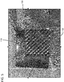
FIG. 5 is a top plan view of a second region of the conductive member ofFIG. 3 shown ultrasonically welded to an example surface. - Reference will now be made in detail to exemplary aspects of the present disclosure that are illustrated in the accompanying drawings. Wherever possible, the same reference numbers will be used throughout the drawings to refer to the same or like parts.
- The present disclosure is directed to an electrical connector that is both mechanically mounted and separately electrically bonded to a surface; and method for forming the electrical bond.
- As shown in
FIGS. 1-2 , aconnection system 100 includes asurface 110, aconnector 120 mounted to thesurface 110, and aconductive member 130 that electrically bonds theconnector 120 to thesurface 110. Theconductive member 130 is formed of a material that may be different from one or both of the surface and theconnector 120. Theconductive member 130 forms an electrical bond between theconnector 120 and thesurface 110. In some implementations, thesurface 110 and theconnector 120 are formed of different materials. In other implementations, however, thesurface 110 and theconnector 120 can be formed of the same material. - The
surface 110 defines anaperture 115 therethrough at which theconnector 120 is mounted. The surface 110-at least around an aperture 115-is formed of a first material. In certain examples, the first material includes Aluminum, such as a 6061-T6 alloy or other Aluminum alloys). Other materials are possible. In certain implementations, thesurface 110 forms a wall of an enclosure holding one or more electrical or electronic components. - The
connector 120 extends through theaperture 115 so that a first end of theconnector 120 is accessible from one side of thesurface 110 and an opposite end of theconnector 120 is accessible from the opposite side of thesurface 110. In some implementations, theconnector 120 terminates a cable at one or both ends. In other implementations, theconnector 120 defines ports at one or both ends to receive a cable plug. In some implementations, theconnector 120 is an electrical connector (e.g., that connects to the electrical or electronic components within the enclosure). In other implementations, theconnector 120 is a fiber optic connector. In other implementations, theconnector 120 is a hybrid connector having both optical and electrical contacts. - In general, the
connector 120 includes anouter body 122 formed of a second material. In some examples, the second material is different from the first material. For example, the first material may include Aluminum while the second material includes steel. Other materials are possible. In other examples, the first and second materials may be the same. - The
connector 120 is mechanically mounted to thesurface 110 at theaperture 115. In an example, theconnector 120 can be threaded to thesurface 110. In other examples, theconnector 120 can be fastened to thesurface 110 with one or more fasteners 128 (e.g., bolts, screws, etc.). In certain examples, theconnector 120 includes anouter body 122 carrying a connection arrangement for electrically and/or optically connecting the first and second ends of theconnector 120. In various examples, the connection arrangement includes one or more electrical contacts 126 (shown schematically inFIG. 1 ), one or more ferrule alignment sleeves, etc. - In certain examples, the
outer body 122 includes aradial mounting flange 124 through which thefasteners 128 can be installed. At least the mountingflange 124 of theouter body 122 is formed of the second material. In certain examples, the second material is sufficiently dissimilar to the first material so as to effectively prohibit direct welding therebetween. In examples, the second material may differ in chemical makeup, hardness, density, or other criteria from the first material. In certain examples, the entire outer body is formed of the second material. In certain examples, the second material includes a corrosion resistant steel. In an example, the second material includes a stainless steel (e.g., 304 stainless steel). Other materials are possible. - In accordance with certain aspects of the disclosure, a
conductive member 130 formed of a third material may be used to form the electrical bonding connection between theelectrical connector 120 and thesurface 110. In certain examples, while theconductive member 130 may provide a weak mechanical connection between theelectrical connector 120 and thesurface 110, theelectrical connector 120 is separately connected to thesurface 110 with a more robust mechanical connection (e.g., threading, fasteners, etc.). - The third material is electrically conductive. In certain implementations, the third material is compatible with the first material for welding (e.g., ultrasonic welding) and is compatible with the second material for welding (e.g., ultrasonic welding). In certain examples, the third material includes Nickel. Other materials, such as copper, are possible.
- The
conductive member 130 has afirst region 132 and asecond region 134. Thefirst region 132 is welded (e.g., ultrasonically) to theouter body 122 of theelectrical connector 120. The weld provides electrical bonding stability between the first and third materials. Thesecond region 134 is welded (e.g., ultrasonically) to thesurface 110. The weld provides electrical bonding stability between the second and third materials. Accordingly, theconductive member 130 provides a current path between the first and second materials. - In certain implementations, the first and
second regions conductive member 130. Other configurations are possible. In some implementations, theconductive member 130 includes a flexible sheet that can be formed into a desired shape or otherwise easily fitted between theconnector 120 and thesurface 110. In certain examples, theconductive member 130 includes foil. In other implementations, theconductive member 130 has a rigid formation that is designed to extend between the connectorouter body 122 and thesurface 110. The first andsecond regions - In use, the
outer body 122 of theconnector 120 is attached to thesurface 110 using a mechanical connection. For example, a mountingflange 124 may be laid over thesurface 110 andbolts 128 may be installed through corners of the mountingflange 124 and into thesurface 110. Aconductive member 130 is positioned between the outer body 122 (e.g., the mounting flange 124) and thesurface 110. For example, a piece of foil may be spread over thesurface 110 and mountingflange 124. - In certain examples, pressure is applied between the
first region 132 of theconductive member 130 and the connector body 122 (e.g., at the mounting flange 124). Then, thefirst region 132 is ultrasonically welded to theouter body 122 using a welding device to create an electrical bond between theconnector body 122 and theconductive member 130. Thesecond region 134 is ultrasonically welded to thesurface 110 using the welding device to create an electrical bond between thesurface 110 and theconductive member 130. - In certain implementations, the
conductive member 130 creates a sufficient electrical pathway so that the electrical bonding resistance between the connectorouter body 122 and thesurface 110 is no more than 5 milliohms. In certain implementations, theconductive member 130 creates a sufficient electrical pathway so that the electrical bonding resistance between the connectorouter body 122 and thesurface 110 is no more than 4 milliohms. In certain implementations, theconductive member 130 creates a sufficient electrical pathway so that the electrical bonding resistance between the connectorouter body 122 and thesurface 110 is no more than 3 milliohms. In certain implementations, theconductive member 130 creates a sufficient electrical pathway so that the electrical bonding resistance between the connectorouter body 122 and thesurface 110 is no more than 2.5 milliohms. In certain implementations, theconductive member 130 creates a sufficient electrical pathway so that the electrical bonding resistance between the connectorouter body 122 and thesurface 110 is less than 2.5 milliohms. - In certain implementations, the welding device includes a press, an anvil, a generator, and a dispenser. The press holds two components (e.g., the connector and the conductive member and/or the surface and the conductive member) under pressure. The pressed components are mounted to the anvil. The generator produces high powered electrical signals that are converted to ultrasonic acoustic vibrations by dispenser. For example, the dispenser may include a piezoelectric transducer or other such converter. The dispenser also includes a horn to emit the acoustic vibrations.
- In certain implementations, the
conductive member 130 covers or substantially covers the seams between theconnector 120 and thesurface 110. In such implementations, theconductive member 130 may provide some EMI shielding to the electronics provided within the enclosure or otherwise on the other side of thesurface 110. - In certain implementations, ultrasonically welding forms a pattern of welds with breaks in between. For example,
FIGS. 3-5 illustrate example ultrasonic welds. InFIGS. 3 and4 , afirst portion 132 of aconductive member 130 is ultrasonically welded to a mountingplate 124 of aconnector 120. InFIG. 5 , asecond portion 134 of theconductive member 130 is ultrasonically welded to asurface 110. As shown, a plurality of solid-state welds extend over theregions FIG. 1 ) between adjacent welds defines the maximum wavelength capable of passing through theconductive member 130. For example, only electromagnetic waves having half-wavelengths smaller than the gap length G may be able to pass through the weld cage of theconductive member 130. - In some implementations, the
conductive member 130 extends around a perimeter of theconnector 120. For example, theconductive member 130 can be shaped to fit over the mountingplate 124 andsurface 110 while accommodating the mechanical connection therebetween. In other implementations, theconductive member 130 is one of a plurality ofconductive members 130 that cooperate to cover at least part of the seam between theconnector 120 and thesurface 110. In the example shown inFIG. 1 , fourconductive members 130 cover the seam-oneconductive member 130 for each side of the mountingflange 124. When multipleconductive members 130 are utilized, a gap length L (FIG. 1 ) between adjacent ones of theconductive members 130 defines the maximum wavelength capable of passing between theconductive members 130. For example, only electromagnetic waves having half-wavelengths smaller than the gap length L may be able to pass between theconductive members 130. Accordingly, EMI stress can be managed within a predetermined tolerance by appropriately spacing theconductive members 130 relative to each other. - Using multiple
conductive members 130 may allow for better accommodation of the mechanical connection (e.g., allow space for the fasteners 128). Alternatively, space for the mechanical connection can be provided in a single-piece conductive member. For example, a sheet of foil may be extended over the connector with a hole punched out for the main connector body andcontacts 126 and additional holes punched out for thefasteners 128. - Having described the preferred aspects and implementations of the present disclosure, modifications and equivalents of the disclosed concepts may readily occur to one skilled in the art. However, it is intended that such modifications and equivalents be included within the scope of the claims which are appended hereto.
Claims (15)
- A connection system comprising:a surface defining an aperture, the surface being formed of a first material;a connector mounted to the surface at the aperture with a mechanical connection, the connector including an outer body carrying a connection arrangement, the outer body being formed of a second material; anda conductive member having a first region and a second region, the first region of the conductive member being ultrasonically welded to the outer body of the connector, the second region of the conductive member being ultrasonically welded to the surface, the conductive member being formed of a third material that is different from the first and second materials, the conductive member electrically connecting together the outer body of the connector and the surface.
- The connection system of claim 1, wherein the second material is different from the first material.
- The connection system of claim 1, wherein the surface forms a wall of an enclosure.
- The connection system of claim 1, wherein the mechanical connection includes a plurality of bolts extending through both the electrical connector and the surface, wherein the outer body of electrical connector includes a mounting flange, the mounting flange defining apertures for receiving the bolts, wherein the first region of the conductive member extends over the mounting flange and the second region of the conductive member extends over the surface.
- The connection system of any of claims 1-4, wherein the first region of the conductive member is ultrasonically welded using a plurality of welds; and , wherein the second region of the conductive member is ultrasonically welded using a plurality of welds, wherein breaks between the welds have lengths that do not exceed a maximum allowable wavelength of an electro-magnetic stress wave.
- The connection system of any of claims 1-4, wherein the conductive member is one of a plurality of conductive members that each have a respective first region ultrasonically welded to the outer body of the electrical connector and a respective second region ultrasonically welded to the surface.
- The connection system of claim 6, wherein the plurality of conductive members covers at least a majority of a perimeter of the electrical connector.
- The connection system of any of claims 1-4, wherein the outer body of the electrical connector directly contacts the surface.
- The connection system of any of claims 1-4, further comprising an EMI gasket disposed between the outer body of the electrical connector and the surface.
- The connection system of any of claims 1-4, wherein the conductive member is a rigid structure extending between the outer body of the electrical connector and the surface.
- The connection system of any of claims 1-4, wherein the conductive member includes a flexible sheet.
- The connection system of any of claims 1-4, wherein the first material includes aluminum, such as an aluminum alloy; and , wherein the second material is stainless steel, such as 304 grade stainless steel.
- The connection system of any of claims 1-4, wherein the conductive member electrically connects the outer body of the electrical connector and the surface to have a bonding resistance of less than 2.5 milliohms.
- The connection system as claimed in claim 3, wherein:the enclosure holds electronics;the connection arrangement has a first end accessible from an interior of the enclosure and a second end accessible from an exterior of the enclosure; andthe conductive member forming part of a conductive arrangement, the conductive arrangement being separate from the mechanical connection, the conductive arrangement extending over a majority of a seam between the connector and the wall.
- A method of creating bonding resistance stability between a connector and a surface of dissimilar materials, the method comprising:attaching the connector to the surface using a mechanical connection;ultrasonically welding a first portion of a conductive member to the connector, the conductive member being formed of a material that is different from the materials of both the connector and the surface;ultrasonically welding a second portion of the conductive member to the surface to create an electrical bond between the connector and the surface, the conductive member being separate from the mechanical connection.
Applications Claiming Priority (1)
| Application Number | Priority Date | Filing Date | Title |
|---|---|---|---|
| US201962940486P | 2019-11-26 | 2019-11-26 |
Publications (2)
| Publication Number | Publication Date |
|---|---|
| EP3829000A1 true EP3829000A1 (en) | 2021-06-02 |
| EP3829000B1 EP3829000B1 (en) | 2023-02-15 |
Family
ID=73597819
Family Applications (1)
| Application Number | Title | Priority Date | Filing Date |
|---|---|---|---|
| EP20209587.3A Active EP3829000B1 (en) | 2019-11-26 | 2020-11-24 | Bonding resistance and electromagnetic interference management of a surface mounted connector |
Country Status (2)
| Country | Link |
|---|---|
| US (1) | US11581689B2 (en) |
| EP (1) | EP3829000B1 (en) |
Citations (5)
| Publication number | Priority date | Publication date | Assignee | Title |
|---|---|---|---|---|
| US20060234528A1 (en) * | 2005-04-13 | 2006-10-19 | Denso Corporation | Electronic apparatus and method for manufacturing the same |
| JP2006331803A (en) * | 2005-05-25 | 2006-12-07 | Denso Corp | Electronic control device |
| EP2104188A1 (en) * | 2008-03-19 | 2009-09-23 | Rohde & Schwarz GmbH & Co. KG | High frequency seal for high frequency connectors |
| EP3163690A1 (en) * | 2015-10-30 | 2017-05-03 | IMS Connector Systems GmbH | Plug with spring basket on connection side |
| DE102018202955A1 (en) * | 2018-02-28 | 2019-08-29 | Robert Bosch Gmbh | Connector system and method of making a connector system |
Family Cites Families (8)
| Publication number | Priority date | Publication date | Assignee | Title |
|---|---|---|---|---|
| US3254402A (en) | 1962-05-09 | 1966-06-07 | Cavitron Ultrasonics Inc | Method and apparatus for joining sheet materials |
| US3376179A (en) | 1964-06-12 | 1968-04-02 | Cavitron Ultrasonics Inc | Method and apparatus for high frequency joining or sealing of thermosoftening materials |
| GB1534265A (en) | 1974-12-04 | 1978-11-29 | Kerry Ultrasonics | Welding thermoplastics materials |
| JP3315314B2 (en) * | 1996-05-30 | 2002-08-19 | 矢崎総業株式会社 | Low insertion force connector |
| DE19916074C2 (en) * | 1999-04-09 | 2002-01-17 | Framatome Connectors Int | Electrical connector, in particular for motor vehicle applications |
| JP3726641B2 (en) * | 2000-05-23 | 2005-12-14 | 住友電装株式会社 | Lever type connector |
| US6811417B2 (en) * | 2003-02-18 | 2004-11-02 | Calsonic Kansei Corporation | Connector structure |
| US6767231B1 (en) * | 2003-09-25 | 2004-07-27 | Tyco Electronics Corporation | Electrical connector with flexible blocking feature |
-
2020
- 2020-11-24 EP EP20209587.3A patent/EP3829000B1/en active Active
- 2020-11-25 US US17/104,143 patent/US11581689B2/en active Active
Patent Citations (5)
| Publication number | Priority date | Publication date | Assignee | Title |
|---|---|---|---|---|
| US20060234528A1 (en) * | 2005-04-13 | 2006-10-19 | Denso Corporation | Electronic apparatus and method for manufacturing the same |
| JP2006331803A (en) * | 2005-05-25 | 2006-12-07 | Denso Corp | Electronic control device |
| EP2104188A1 (en) * | 2008-03-19 | 2009-09-23 | Rohde & Schwarz GmbH & Co. KG | High frequency seal for high frequency connectors |
| EP3163690A1 (en) * | 2015-10-30 | 2017-05-03 | IMS Connector Systems GmbH | Plug with spring basket on connection side |
| DE102018202955A1 (en) * | 2018-02-28 | 2019-08-29 | Robert Bosch Gmbh | Connector system and method of making a connector system |
Also Published As
| Publication number | Publication date |
|---|---|
| EP3829000B1 (en) | 2023-02-15 |
| US20210159655A1 (en) | 2021-05-27 |
| US11581689B2 (en) | 2023-02-14 |
Similar Documents
| Publication | Publication Date | Title |
|---|---|---|
| CN104253252B (en) | battery module | |
| CN104348041B (en) | Electronic device module | |
| US7094970B2 (en) | Shielded wire harness | |
| JP5970825B2 (en) | undercover | |
| EP2153777A1 (en) | Ultrasonic probe and ultrasonic diagnosis device | |
| JP2020509545A (en) | Frame assembly and method for manufacturing the same | |
| US6528731B2 (en) | Flat shield harness and method for manufacturing the same | |
| CZ232198A3 (en) | Control apparatus, particularly for motor vehicle | |
| UA106745C2 (en) | FINAL PROCESSING UNIT for CONNECTION of shielding of armored cable | |
| CN112652863A (en) | Method of connecting battery cells in a battery array | |
| JP6432395B2 (en) | Electronic equipment | |
| US9475232B2 (en) | Damping and isolating vibration during ultrasonic welding | |
| CN110495057B (en) | Connector with a locking member | |
| US11581689B2 (en) | Bonding resistance and electromagnetic interference management of a surface mounted connector | |
| WO2014061727A1 (en) | Shield connector | |
| JP2019050516A (en) | Camera device | |
| US12607531B2 (en) | Split-type piezoelectric sensor | |
| JP6949104B2 (en) | Battery pack and battery pack manufacturing method | |
| CN1350715A (en) | Vibrator assembly for mobile telephone | |
| JPH08274486A (en) | Electronics | |
| JP6782830B2 (en) | Battery module | |
| JP5115518B2 (en) | Electronic equipment | |
| KR102396103B1 (en) | Connector and converter | |
| CN210326234U (en) | Conductive connectors and electrical equipment | |
| US6977336B2 (en) | Electronic device |
Legal Events
| Date | Code | Title | Description |
|---|---|---|---|
| PUAI | Public reference made under article 153(3) epc to a published international application that has entered the european phase |
Free format text: ORIGINAL CODE: 0009012 |
|
| STAA | Information on the status of an ep patent application or granted ep patent |
Free format text: STATUS: REQUEST FOR EXAMINATION WAS MADE |
|
| 17P | Request for examination filed |
Effective date: 20201124 |
|
| AK | Designated contracting states |
Kind code of ref document: A1 Designated state(s): AL AT BE BG CH CY CZ DE DK EE ES FI FR GB GR HR HU IE IS IT LI LT LU LV MC MK MT NL NO PL PT RO RS SE SI SK SM TR |
|
| GRAP | Despatch of communication of intention to grant a patent |
Free format text: ORIGINAL CODE: EPIDOSNIGR1 |
|
| STAA | Information on the status of an ep patent application or granted ep patent |
Free format text: STATUS: GRANT OF PATENT IS INTENDED |
|
| RIC1 | Information provided on ipc code assigned before grant |
Ipc: H01R 13/6596 20110101ALN20220922BHEP Ipc: H01R 4/62 20060101ALI20220922BHEP Ipc: H01R 43/02 20060101ALI20220922BHEP Ipc: H01R 13/74 20060101ALI20220922BHEP Ipc: H01R 4/64 20060101ALI20220922BHEP Ipc: H01R 4/02 20060101AFI20220922BHEP |
|
| INTG | Intention to grant announced |
Effective date: 20221010 |
|
| GRAS | Grant fee paid |
Free format text: ORIGINAL CODE: EPIDOSNIGR3 |
|
| GRAA | (expected) grant |
Free format text: ORIGINAL CODE: 0009210 |
|
| STAA | Information on the status of an ep patent application or granted ep patent |
Free format text: STATUS: THE PATENT HAS BEEN GRANTED |
|
| AK | Designated contracting states |
Kind code of ref document: B1 Designated state(s): AL AT BE BG CH CY CZ DE DK EE ES FI FR GB GR HR HU IE IS IT LI LT LU LV MC MK MT NL NO PL PT RO RS SE SI SK SM TR |
|
| REG | Reference to a national code |
Ref country code: CH Ref legal event code: EP Ref country code: GB Ref legal event code: FG4D |
|
| REG | Reference to a national code |
Ref country code: DE Ref legal event code: R096 Ref document number: 602020008092 Country of ref document: DE |
|
| REG | Reference to a national code |
Ref country code: AT Ref legal event code: REF Ref document number: 1548729 Country of ref document: AT Kind code of ref document: T Effective date: 20230315 Ref country code: IE Ref legal event code: FG4D |
|
| REG | Reference to a national code |
Ref country code: LT Ref legal event code: MG9D |
|
| REG | Reference to a national code |
Ref country code: NL Ref legal event code: MP Effective date: 20230215 |
|
| P01 | Opt-out of the competence of the unified patent court (upc) registered |
Effective date: 20230521 |
|
| REG | Reference to a national code |
Ref country code: AT Ref legal event code: MK05 Ref document number: 1548729 Country of ref document: AT Kind code of ref document: T Effective date: 20230215 |
|
| PG25 | Lapsed in a contracting state [announced via postgrant information from national office to epo] |
Ref country code: RS Free format text: LAPSE BECAUSE OF FAILURE TO SUBMIT A TRANSLATION OF THE DESCRIPTION OR TO PAY THE FEE WITHIN THE PRESCRIBED TIME-LIMIT Effective date: 20230215 Ref country code: PT Free format text: LAPSE BECAUSE OF FAILURE TO SUBMIT A TRANSLATION OF THE DESCRIPTION OR TO PAY THE FEE WITHIN THE PRESCRIBED TIME-LIMIT Effective date: 20230615 Ref country code: NO Free format text: LAPSE BECAUSE OF FAILURE TO SUBMIT A TRANSLATION OF THE DESCRIPTION OR TO PAY THE FEE WITHIN THE PRESCRIBED TIME-LIMIT Effective date: 20230515 Ref country code: NL Free format text: LAPSE BECAUSE OF FAILURE TO SUBMIT A TRANSLATION OF THE DESCRIPTION OR TO PAY THE FEE WITHIN THE PRESCRIBED TIME-LIMIT Effective date: 20230215 Ref country code: LV Free format text: LAPSE BECAUSE OF FAILURE TO SUBMIT A TRANSLATION OF THE DESCRIPTION OR TO PAY THE FEE WITHIN THE PRESCRIBED TIME-LIMIT Effective date: 20230215 Ref country code: LT Free format text: LAPSE BECAUSE OF FAILURE TO SUBMIT A TRANSLATION OF THE DESCRIPTION OR TO PAY THE FEE WITHIN THE PRESCRIBED TIME-LIMIT Effective date: 20230215 Ref country code: HR Free format text: LAPSE BECAUSE OF FAILURE TO SUBMIT A TRANSLATION OF THE DESCRIPTION OR TO PAY THE FEE WITHIN THE PRESCRIBED TIME-LIMIT Effective date: 20230215 Ref country code: ES Free format text: LAPSE BECAUSE OF FAILURE TO SUBMIT A TRANSLATION OF THE DESCRIPTION OR TO PAY THE FEE WITHIN THE PRESCRIBED TIME-LIMIT Effective date: 20230215 Ref country code: AT Free format text: LAPSE BECAUSE OF FAILURE TO SUBMIT A TRANSLATION OF THE DESCRIPTION OR TO PAY THE FEE WITHIN THE PRESCRIBED TIME-LIMIT Effective date: 20230215 |
|
| PG25 | Lapsed in a contracting state [announced via postgrant information from national office to epo] |
Ref country code: SE Free format text: LAPSE BECAUSE OF FAILURE TO SUBMIT A TRANSLATION OF THE DESCRIPTION OR TO PAY THE FEE WITHIN THE PRESCRIBED TIME-LIMIT Effective date: 20230215 Ref country code: PL Free format text: LAPSE BECAUSE OF FAILURE TO SUBMIT A TRANSLATION OF THE DESCRIPTION OR TO PAY THE FEE WITHIN THE PRESCRIBED TIME-LIMIT Effective date: 20230215 Ref country code: IS Free format text: LAPSE BECAUSE OF FAILURE TO SUBMIT A TRANSLATION OF THE DESCRIPTION OR TO PAY THE FEE WITHIN THE PRESCRIBED TIME-LIMIT Effective date: 20230615 Ref country code: GR Free format text: LAPSE BECAUSE OF FAILURE TO SUBMIT A TRANSLATION OF THE DESCRIPTION OR TO PAY THE FEE WITHIN THE PRESCRIBED TIME-LIMIT Effective date: 20230516 Ref country code: FI Free format text: LAPSE BECAUSE OF FAILURE TO SUBMIT A TRANSLATION OF THE DESCRIPTION OR TO PAY THE FEE WITHIN THE PRESCRIBED TIME-LIMIT Effective date: 20230215 |
|
| PG25 | Lapsed in a contracting state [announced via postgrant information from national office to epo] |
Ref country code: SM Free format text: LAPSE BECAUSE OF FAILURE TO SUBMIT A TRANSLATION OF THE DESCRIPTION OR TO PAY THE FEE WITHIN THE PRESCRIBED TIME-LIMIT Effective date: 20230215 Ref country code: RO Free format text: LAPSE BECAUSE OF FAILURE TO SUBMIT A TRANSLATION OF THE DESCRIPTION OR TO PAY THE FEE WITHIN THE PRESCRIBED TIME-LIMIT Effective date: 20230215 Ref country code: EE Free format text: LAPSE BECAUSE OF FAILURE TO SUBMIT A TRANSLATION OF THE DESCRIPTION OR TO PAY THE FEE WITHIN THE PRESCRIBED TIME-LIMIT Effective date: 20230215 Ref country code: DK Free format text: LAPSE BECAUSE OF FAILURE TO SUBMIT A TRANSLATION OF THE DESCRIPTION OR TO PAY THE FEE WITHIN THE PRESCRIBED TIME-LIMIT Effective date: 20230215 Ref country code: CZ Free format text: LAPSE BECAUSE OF FAILURE TO SUBMIT A TRANSLATION OF THE DESCRIPTION OR TO PAY THE FEE WITHIN THE PRESCRIBED TIME-LIMIT Effective date: 20230215 |
|
| REG | Reference to a national code |
Ref country code: DE Ref legal event code: R097 Ref document number: 602020008092 Country of ref document: DE |
|
| PG25 | Lapsed in a contracting state [announced via postgrant information from national office to epo] |
Ref country code: SK Free format text: LAPSE BECAUSE OF FAILURE TO SUBMIT A TRANSLATION OF THE DESCRIPTION OR TO PAY THE FEE WITHIN THE PRESCRIBED TIME-LIMIT Effective date: 20230215 |
|
| PLBE | No opposition filed within time limit |
Free format text: ORIGINAL CODE: 0009261 |
|
| STAA | Information on the status of an ep patent application or granted ep patent |
Free format text: STATUS: NO OPPOSITION FILED WITHIN TIME LIMIT |
|
| 26N | No opposition filed |
Effective date: 20231116 |
|
| PG25 | Lapsed in a contracting state [announced via postgrant information from national office to epo] |
Ref country code: SI Free format text: LAPSE BECAUSE OF FAILURE TO SUBMIT A TRANSLATION OF THE DESCRIPTION OR TO PAY THE FEE WITHIN THE PRESCRIBED TIME-LIMIT Effective date: 20230215 |
|
| PG25 | Lapsed in a contracting state [announced via postgrant information from national office to epo] |
Ref country code: IT Free format text: LAPSE BECAUSE OF FAILURE TO SUBMIT A TRANSLATION OF THE DESCRIPTION OR TO PAY THE FEE WITHIN THE PRESCRIBED TIME-LIMIT Effective date: 20230215 |
|
| REG | Reference to a national code |
Ref country code: CH Ref legal event code: PL |
|
| PG25 | Lapsed in a contracting state [announced via postgrant information from national office to epo] |
Ref country code: MC Free format text: LAPSE BECAUSE OF FAILURE TO SUBMIT A TRANSLATION OF THE DESCRIPTION OR TO PAY THE FEE WITHIN THE PRESCRIBED TIME-LIMIT Effective date: 20230215 |
|
| PG25 | Lapsed in a contracting state [announced via postgrant information from national office to epo] |
Ref country code: LU Free format text: LAPSE BECAUSE OF NON-PAYMENT OF DUE FEES Effective date: 20231124 |
|
| PG25 | Lapsed in a contracting state [announced via postgrant information from national office to epo] |
Ref country code: CH Free format text: LAPSE BECAUSE OF NON-PAYMENT OF DUE FEES Effective date: 20231130 |
|
| PG25 | Lapsed in a contracting state [announced via postgrant information from national office to epo] |
Ref country code: MC Free format text: LAPSE BECAUSE OF FAILURE TO SUBMIT A TRANSLATION OF THE DESCRIPTION OR TO PAY THE FEE WITHIN THE PRESCRIBED TIME-LIMIT Effective date: 20230215 Ref country code: LU Free format text: LAPSE BECAUSE OF NON-PAYMENT OF DUE FEES Effective date: 20231124 Ref country code: CH Free format text: LAPSE BECAUSE OF NON-PAYMENT OF DUE FEES Effective date: 20231130 |
|
| REG | Reference to a national code |
Ref country code: BE Ref legal event code: MM Effective date: 20231130 |
|
| REG | Reference to a national code |
Ref country code: IE Ref legal event code: MM4A |
|
| PG25 | Lapsed in a contracting state [announced via postgrant information from national office to epo] |
Ref country code: IE Free format text: LAPSE BECAUSE OF NON-PAYMENT OF DUE FEES Effective date: 20231124 |
|
| PG25 | Lapsed in a contracting state [announced via postgrant information from national office to epo] |
Ref country code: BE Free format text: LAPSE BECAUSE OF NON-PAYMENT OF DUE FEES Effective date: 20231130 |
|
| PG25 | Lapsed in a contracting state [announced via postgrant information from national office to epo] |
Ref country code: IE Free format text: LAPSE BECAUSE OF NON-PAYMENT OF DUE FEES Effective date: 20231124 Ref country code: BE Free format text: LAPSE BECAUSE OF NON-PAYMENT OF DUE FEES Effective date: 20231130 |
|
| PG25 | Lapsed in a contracting state [announced via postgrant information from national office to epo] |
Ref country code: BG Free format text: LAPSE BECAUSE OF FAILURE TO SUBMIT A TRANSLATION OF THE DESCRIPTION OR TO PAY THE FEE WITHIN THE PRESCRIBED TIME-LIMIT Effective date: 20230215 |
|
| PG25 | Lapsed in a contracting state [announced via postgrant information from national office to epo] |
Ref country code: BG Free format text: LAPSE BECAUSE OF FAILURE TO SUBMIT A TRANSLATION OF THE DESCRIPTION OR TO PAY THE FEE WITHIN THE PRESCRIBED TIME-LIMIT Effective date: 20230215 |
|
| GBPC | Gb: european patent ceased through non-payment of renewal fee |
Effective date: 20241124 |
|
| PG25 | Lapsed in a contracting state [announced via postgrant information from national office to epo] |
Ref country code: CY Free format text: LAPSE BECAUSE OF FAILURE TO SUBMIT A TRANSLATION OF THE DESCRIPTION OR TO PAY THE FEE WITHIN THE PRESCRIBED TIME-LIMIT; INVALID AB INITIO Effective date: 20201124 |
|
| PG25 | Lapsed in a contracting state [announced via postgrant information from national office to epo] |
Ref country code: HU Free format text: LAPSE BECAUSE OF FAILURE TO SUBMIT A TRANSLATION OF THE DESCRIPTION OR TO PAY THE FEE WITHIN THE PRESCRIBED TIME-LIMIT; INVALID AB INITIO Effective date: 20201124 |
|
| PG25 | Lapsed in a contracting state [announced via postgrant information from national office to epo] |
Ref country code: GB Free format text: LAPSE BECAUSE OF NON-PAYMENT OF DUE FEES Effective date: 20241124 |
|
| PG25 | Lapsed in a contracting state [announced via postgrant information from national office to epo] |
Ref country code: TR Free format text: LAPSE BECAUSE OF FAILURE TO SUBMIT A TRANSLATION OF THE DESCRIPTION OR TO PAY THE FEE WITHIN THE PRESCRIBED TIME-LIMIT Effective date: 20230215 |
|
| PGFP | Annual fee paid to national office [announced via postgrant information from national office to epo] |
Ref country code: DE Payment date: 20251022 Year of fee payment: 6 |
|
| PGFP | Annual fee paid to national office [announced via postgrant information from national office to epo] |
Ref country code: FR Payment date: 20251022 Year of fee payment: 6 |