EP3826435A1 - Member for plasma processing device - Google Patents
Member for plasma processing device Download PDFInfo
- Publication number
- EP3826435A1 EP3826435A1 EP19838458.8A EP19838458A EP3826435A1 EP 3826435 A1 EP3826435 A1 EP 3826435A1 EP 19838458 A EP19838458 A EP 19838458A EP 3826435 A1 EP3826435 A1 EP 3826435A1
- Authority
- EP
- European Patent Office
- Prior art keywords
- oxide film
- processing device
- plasma processing
- base material
- film
- Prior art date
- Legal status (The legal status is an assumption and is not a legal conclusion. Google has not performed a legal analysis and makes no representation as to the accuracy of the status listed.)
- Pending
Links
Images


Classifications
-
- H—ELECTRICITY
- H01—ELECTRIC ELEMENTS
- H01J—ELECTRIC DISCHARGE TUBES OR DISCHARGE LAMPS
- H01J37/00—Discharge tubes with provision for introducing objects or material to be exposed to the discharge, e.g. for the purpose of examination or processing thereof
- H01J37/32—Gas-filled discharge tubes
- H01J37/32431—Constructional details of the reactor
- H01J37/32458—Vessel
- H01J37/32477—Vessel characterised by the means for protecting vessels or internal parts, e.g. coatings
-
- C—CHEMISTRY; METALLURGY
- C23—COATING METALLIC MATERIAL; COATING MATERIAL WITH METALLIC MATERIAL; CHEMICAL SURFACE TREATMENT; DIFFUSION TREATMENT OF METALLIC MATERIAL; COATING BY VACUUM EVAPORATION, BY SPUTTERING, BY ION IMPLANTATION OR BY CHEMICAL VAPOUR DEPOSITION, IN GENERAL; INHIBITING CORROSION OF METALLIC MATERIAL OR INCRUSTATION IN GENERAL
- C23C—COATING METALLIC MATERIAL; COATING MATERIAL WITH METALLIC MATERIAL; SURFACE TREATMENT OF METALLIC MATERIAL BY DIFFUSION INTO THE SURFACE, BY CHEMICAL CONVERSION OR SUBSTITUTION; COATING BY VACUUM EVAPORATION, BY SPUTTERING, BY ION IMPLANTATION OR BY CHEMICAL VAPOUR DEPOSITION, IN GENERAL
- C23C28/00—Coating for obtaining at least two superposed coatings either by methods not provided for in a single one of groups C23C2/00 - C23C26/00 or by combinations of methods provided for in subclasses C23C and C25C or C25D
- C23C28/04—Coating for obtaining at least two superposed coatings either by methods not provided for in a single one of groups C23C2/00 - C23C26/00 or by combinations of methods provided for in subclasses C23C and C25C or C25D only coatings of inorganic non-metallic material
- C23C28/042—Coating for obtaining at least two superposed coatings either by methods not provided for in a single one of groups C23C2/00 - C23C26/00 or by combinations of methods provided for in subclasses C23C and C25C or C25D only coatings of inorganic non-metallic material including a refractory ceramic layer, e.g. refractory metal oxides, ZrO2, rare earth oxides
-
- C—CHEMISTRY; METALLURGY
- C23—COATING METALLIC MATERIAL; COATING MATERIAL WITH METALLIC MATERIAL; CHEMICAL SURFACE TREATMENT; DIFFUSION TREATMENT OF METALLIC MATERIAL; COATING BY VACUUM EVAPORATION, BY SPUTTERING, BY ION IMPLANTATION OR BY CHEMICAL VAPOUR DEPOSITION, IN GENERAL; INHIBITING CORROSION OF METALLIC MATERIAL OR INCRUSTATION IN GENERAL
- C23C—COATING METALLIC MATERIAL; COATING MATERIAL WITH METALLIC MATERIAL; SURFACE TREATMENT OF METALLIC MATERIAL BY DIFFUSION INTO THE SURFACE, BY CHEMICAL CONVERSION OR SUBSTITUTION; COATING BY VACUUM EVAPORATION, BY SPUTTERING, BY ION IMPLANTATION OR BY CHEMICAL VAPOUR DEPOSITION, IN GENERAL
- C23C28/00—Coating for obtaining at least two superposed coatings either by methods not provided for in a single one of groups C23C2/00 - C23C26/00 or by combinations of methods provided for in subclasses C23C and C25C or C25D
- C23C28/04—Coating for obtaining at least two superposed coatings either by methods not provided for in a single one of groups C23C2/00 - C23C26/00 or by combinations of methods provided for in subclasses C23C and C25C or C25D only coatings of inorganic non-metallic material
-
- C—CHEMISTRY; METALLURGY
- C23—COATING METALLIC MATERIAL; COATING MATERIAL WITH METALLIC MATERIAL; CHEMICAL SURFACE TREATMENT; DIFFUSION TREATMENT OF METALLIC MATERIAL; COATING BY VACUUM EVAPORATION, BY SPUTTERING, BY ION IMPLANTATION OR BY CHEMICAL VAPOUR DEPOSITION, IN GENERAL; INHIBITING CORROSION OF METALLIC MATERIAL OR INCRUSTATION IN GENERAL
- C23C—COATING METALLIC MATERIAL; COATING MATERIAL WITH METALLIC MATERIAL; SURFACE TREATMENT OF METALLIC MATERIAL BY DIFFUSION INTO THE SURFACE, BY CHEMICAL CONVERSION OR SUBSTITUTION; COATING BY VACUUM EVAPORATION, BY SPUTTERING, BY ION IMPLANTATION OR BY CHEMICAL VAPOUR DEPOSITION, IN GENERAL
- C23C28/00—Coating for obtaining at least two superposed coatings either by methods not provided for in a single one of groups C23C2/00 - C23C26/00 or by combinations of methods provided for in subclasses C23C and C25C or C25D
- C23C28/04—Coating for obtaining at least two superposed coatings either by methods not provided for in a single one of groups C23C2/00 - C23C26/00 or by combinations of methods provided for in subclasses C23C and C25C or C25D only coatings of inorganic non-metallic material
- C23C28/048—Coating for obtaining at least two superposed coatings either by methods not provided for in a single one of groups C23C2/00 - C23C26/00 or by combinations of methods provided for in subclasses C23C and C25C or C25D only coatings of inorganic non-metallic material with layers graded in composition or physical properties
-
- C—CHEMISTRY; METALLURGY
- C23—COATING METALLIC MATERIAL; COATING MATERIAL WITH METALLIC MATERIAL; CHEMICAL SURFACE TREATMENT; DIFFUSION TREATMENT OF METALLIC MATERIAL; COATING BY VACUUM EVAPORATION, BY SPUTTERING, BY ION IMPLANTATION OR BY CHEMICAL VAPOUR DEPOSITION, IN GENERAL; INHIBITING CORROSION OF METALLIC MATERIAL OR INCRUSTATION IN GENERAL
- C23C—COATING METALLIC MATERIAL; COATING MATERIAL WITH METALLIC MATERIAL; SURFACE TREATMENT OF METALLIC MATERIAL BY DIFFUSION INTO THE SURFACE, BY CHEMICAL CONVERSION OR SUBSTITUTION; COATING BY VACUUM EVAPORATION, BY SPUTTERING, BY ION IMPLANTATION OR BY CHEMICAL VAPOUR DEPOSITION, IN GENERAL
- C23C4/00—Coating by spraying the coating material in the molten state, e.g. by flame, plasma or electric discharge
- C23C4/04—Coating by spraying the coating material in the molten state, e.g. by flame, plasma or electric discharge characterised by the coating material
- C23C4/10—Oxides, borides, carbides, nitrides or silicides; Mixtures thereof
-
- C—CHEMISTRY; METALLURGY
- C25—ELECTROLYTIC OR ELECTROPHORETIC PROCESSES; APPARATUS THEREFOR
- C25D—PROCESSES FOR THE ELECTROLYTIC OR ELECTROPHORETIC PRODUCTION OF COATINGS; ELECTROFORMING; APPARATUS THEREFOR
- C25D11/00—Electrolytic coating by surface reaction, i.e. forming conversion layers
- C25D11/02—Anodisation
- C25D11/04—Anodisation of aluminium or alloys based thereon
- C25D11/12—Anodising more than once, e.g. in different baths
-
- C—CHEMISTRY; METALLURGY
- C25—ELECTROLYTIC OR ELECTROPHORETIC PROCESSES; APPARATUS THEREFOR
- C25D—PROCESSES FOR THE ELECTROLYTIC OR ELECTROPHORETIC PRODUCTION OF COATINGS; ELECTROFORMING; APPARATUS THEREFOR
- C25D11/00—Electrolytic coating by surface reaction, i.e. forming conversion layers
- C25D11/02—Anodisation
- C25D11/04—Anodisation of aluminium or alloys based thereon
- C25D11/18—After-treatment, e.g. pore-sealing
-
- C—CHEMISTRY; METALLURGY
- C25—ELECTROLYTIC OR ELECTROPHORETIC PROCESSES; APPARATUS THEREFOR
- C25D—PROCESSES FOR THE ELECTROLYTIC OR ELECTROPHORETIC PRODUCTION OF COATINGS; ELECTROFORMING; APPARATUS THEREFOR
- C25D11/00—Electrolytic coating by surface reaction, i.e. forming conversion layers
- C25D11/02—Anodisation
- C25D11/04—Anodisation of aluminium or alloys based thereon
- C25D11/18—After-treatment, e.g. pore-sealing
- C25D11/24—Chemical after-treatment
- C25D11/246—Chemical after-treatment for sealing layers
-
- H—ELECTRICITY
- H01—ELECTRIC ELEMENTS
- H01J—ELECTRIC DISCHARGE TUBES OR DISCHARGE LAMPS
- H01J37/00—Discharge tubes with provision for introducing objects or material to be exposed to the discharge, e.g. for the purpose of examination or processing thereof
- H01J37/32—Gas-filled discharge tubes
- H01J37/32431—Constructional details of the reactor
- H01J37/32532—Electrodes
-
- H—ELECTRICITY
- H01—ELECTRIC ELEMENTS
- H01J—ELECTRIC DISCHARGE TUBES OR DISCHARGE LAMPS
- H01J37/00—Discharge tubes with provision for introducing objects or material to be exposed to the discharge, e.g. for the purpose of examination or processing thereof
- H01J37/32—Gas-filled discharge tubes
- H01J37/32431—Constructional details of the reactor
- H01J37/32532—Electrodes
- H01J37/3255—Material
-
- H—ELECTRICITY
- H01—ELECTRIC ELEMENTS
- H01J—ELECTRIC DISCHARGE TUBES OR DISCHARGE LAMPS
- H01J37/00—Discharge tubes with provision for introducing objects or material to be exposed to the discharge, e.g. for the purpose of examination or processing thereof
- H01J37/32—Gas-filled discharge tubes
- H01J37/32431—Constructional details of the reactor
- H01J37/32532—Electrodes
- H01J37/32559—Protection means, e.g. coatings
-
- H—ELECTRICITY
- H05—ELECTRIC TECHNIQUES NOT OTHERWISE PROVIDED FOR
- H05H—PLASMA TECHNIQUE; PRODUCTION OF ACCELERATED ELECTRICALLY-CHARGED PARTICLES OR OF NEUTRONS; PRODUCTION OR ACCELERATION OF NEUTRAL MOLECULAR OR ATOMIC BEAMS
- H05H1/00—Generating plasma; Handling plasma
- H05H1/24—Generating plasma
- H05H1/2406—Generating plasma using dielectric barrier discharges, i.e. with a dielectric interposed between the electrodes
-
- H—ELECTRICITY
- H05—ELECTRIC TECHNIQUES NOT OTHERWISE PROVIDED FOR
- H05H—PLASMA TECHNIQUE; PRODUCTION OF ACCELERATED ELECTRICALLY-CHARGED PARTICLES OR OF NEUTRONS; PRODUCTION OR ACCELERATION OF NEUTRAL MOLECULAR OR ATOMIC BEAMS
- H05H1/00—Generating plasma; Handling plasma
- H05H1/24—Generating plasma
- H05H1/2406—Generating plasma using dielectric barrier discharges, i.e. with a dielectric interposed between the electrodes
- H05H1/2441—Generating plasma using dielectric barrier discharges, i.e. with a dielectric interposed between the electrodes characterised by the physical-chemical properties of the dielectric, e.g. porous dielectric
-
- H—ELECTRICITY
- H10—SEMICONDUCTOR DEVICES; ELECTRIC SOLID-STATE DEVICES NOT OTHERWISE PROVIDED FOR
- H10P—GENERIC PROCESSES OR APPARATUS FOR THE MANUFACTURE OR TREATMENT OF DEVICES COVERED BY CLASS H10
- H10P50/00—Etching of wafers, substrates or parts of devices
- H10P50/20—Dry etching; Plasma etching; Reactive-ion etching
- H10P50/24—Dry etching; Plasma etching; Reactive-ion etching of semiconductor materials
- H10P50/242—Dry etching; Plasma etching; Reactive-ion etching of semiconductor materials of Group IV materials
Definitions
- the present invention relates to a member for a plasma processing device used for a plasma processing device.
- Patent Literature 1 discloses a member that has, in a vacuum processing device that processes a substrate to be processed based on plasma reaction, oxide film layers formed on the surfaces of electrode bodies disposed in a vacuum processing chamber and has alumina sprayed films formed on the oxide film layers so as to be multilayered. According to Patent Literature 1, oxide film layers are protected by alumina sprayed films so as to prevent cracks and peeling-offs of the oxide film layers and generation of particles is prevented, lifetime is lengthened so as to reduce the replacement frequency, and the availability factor of the device is improved.
- Patent Literature 2 discloses processing of a member that has an oxidation treatment film formed on a surface of a base material, and anodic oxidation processing that includes, in a manufacturing method of an internal member of a plasma-treated vessel that has a sprayed film formed on the oxidation treatment film, a step of immersing the base material in an alkaline organic solvent and a step of generating plasma discharge in the alkaline organic solvent.
- Examples of the internal member of a plasma-treated vessel include electrode protecting members and insulating rings.
- a member for a plasma processing device needs a high withstand voltage due to high energy in a recent plasm processing step.
- an object of the present invention is to provide a member for a plasma processing device having a high withstand voltage.
- a member for a plasma processing device includes: an aluminum base material; and an oxide film formed on the aluminum base material and having a porous structure, the oxide film including a first oxide film formed on a surface of the aluminum base material, a second oxide film formed opposite to an aluminum base material side of the first oxide film, and a third oxide film formed opposite to the first oxide film side of the second oxide film, wherein the first oxide film is harder than the second oxide film and the third oxide film, and a hole formed in each of the first oxide film, the second oxide film and the third oxide film is sealed.
- the above-described member for a plasma processing device includes a ceramic sprayed film formed opposite to the aluminum base material side of the oxide film.
- the second oxide film becomes harder from the third oxide film toward the first oxide film.
- the oxide film has porosity of 1% to 2%.
- the first oxide film includes a barrier layer on a part that contacts the aluminum base material, and the barrier layer has thickness of 80 nm to 210 nm.
- the oxide film is sealed by hydrated alumina, and the hydrated alumina is hydrate of 1.4 to 2.0.
- the oxide film has the thickness of 70 ⁇ m to 130 ⁇ m.
- a member for a plasma processing device having a high withstand voltage can be implemented.
- FIG. 1 is a cross-sectional view illustrating the configuration of a member for a plasma processing device in accordance with the embodiment of the present invention.
- FIG. 2 is a cross-sectional view in which a part (area R) of the member for a plasma processing device illustrated in FIG. 1 is enlarged.
- a member for a plasma processing device 1 illustrated in FIG. 1 includes a base material 10 that is an insulating substrate, an oxide film 20 that is formed on a part of the surface of the base material 10, and a sprayed film 30 that is provided opposite to a base material 10 side of the oxide film 20.
- the member for a plasma processing device 1 is used as a member used for a plasma processing device, for example, electrodes and materials of electrode protecting members and the like, and is formed by processing and the like of a host material formed of the base material 10, the oxide film 20, and the sprayed film 30.
- the base material 10 is an aluminum base material that is formed of aluminum, an alloy mainly consisting of aluminum, or aluminum oxide.
- the sprayed film 30 is a ceramic sprayed film formed of ceramic.
- FIG. 3 is a microscope image illustrating an example of the oxide film in the member for a plasma processing device in accordance with the embodiment of the present invention, and the microscope image illustrating a cross-sectional surface of the oxide film.
- FIGS. 4 and 5 are scanning electron microscope (SEM) images illustrating examples of the oxide film in the member for a plasma processing device in accordance with the embodiment of the present invention, and the SEM images illustrating cross-sectional surfaces of the oxide film.
- FIGS. 3 to 5 illustrate an area (film) corresponding to each part in the oxide film illustrated in FIG. 2 .
- the oxide film 20 is formed of alumite, and is an alumina film formed in three layers.
- the oxide film 20 is formed of a first oxide film 21 formed on a surface of the base material 10, a second oxide film 22 laminated opposite to the base material 10 side of the first oxide film 21, and a third oxide film 23 laminated opposite to the first oxide film 21 side of the second oxide film 22 (for example, see FIGS. 2 and 3 ).
- the first oxide film 21 has hardness higher than that of the second oxide film 22.
- the second oxide film 22 has hardness higher than that of the third oxide film 23.
- the oxide film 20 has lower hardness from the base material 10 toward the sprayed film 30.
- the first oxide film 21 preferably has hardness of 400 Hv or more and 430 Hv or less.
- the second oxide film 22 preferably has hardness of 200 Hv or more and 380 Hv or less.
- the third oxide film 23 preferably has hardness of 40 Hv or more and 80 Hv or less.
- the second oxide film 22 has higher hardness from the third oxide film 23 toward the first oxide film 21.
- first oxide film 21 has hardness of less than 400 Hv, abrasion resistance may be lowered and a withstand voltage may be lowered.
- first oxide film 21 has hardness of more than 430 Hv, cracks may be generated on the first oxide film 21.
- the second oxide film 22 has the longest length and the first oxide film 21 has the shortest length.
- the first oxide film 21 has a length of 80 nm or more and 210 nm or less.
- the second oxide film 22 preferably has a length of 60 ⁇ m or more and 100 ⁇ m or less.
- the third oxide film 23 has a length of 20 ⁇ m or more and 30 ⁇ m or less.
- the oxide film 20 preferably has thickness of 70 ⁇ m or more and 130 ⁇ m or less, and especially, preferably 70 ⁇ m or more and 120 ⁇ m or less.
- the first oxide film 21 includes a film layer 21a formed on the second oxide film 22 side, and a barrier layer 21b formed on the base material 10 side.
- the barrier layer 21b is a non-conductive film formed on a surface of the base material, and is the layer supporting the growth of the film during film formation (film layer 21a).
- the barrier layer 21b preferably has thickness of 80 nm or more and 210 nm or less. In this case, the barrier layer 21b has a content higher than that of the film layer 21a in the first oxide film 21.
- the conventional barrier layer has, in a film equal to the first oxide film 21, thickness of 30 nm to 40 nm.
- the film layer 21a and the barrier layer 21b have the same hardness, and preferably have the hardness described above (400 Hv or more and 430 Hv or less).
- the oxide film 20 has porosity of 1% or more and 2% or less.
- the first oxide film 21, the second oxide film 22, and the third oxide film 23 are porous films, and the respective holes of the first oxide film 21, the second oxide film 22, and the third oxide film 23 are filled with hydrated alumina.
- This hydrated alumina is preferably hydrate of 1.4 or more and 2.0 or less.
- the holes described above are formed on the film layer 21a.
- a method for manufacturing the member for a plasma processing device 1 will be described.
- the base material 10 described above is prepared.
- the oxide film 20 is formed.
- the third oxide film 23 is formed first.
- the second oxide film 22 is formed.
- the first oxide film 21 is formed.
- the film layers are formed by anodic oxidation processing.
- holes formed in the oxide film 20 are filled with hydrated alumina.
- the oxide film 20 is formed on the base material 10.
- the sprayed film 30 is formed opposite to the base material 10 side of the oxide film 20.
- FIG. 6 is a view illustrating physical properties between the member for a plasma processing device in accordance with the embodiment of the present invention and the member for a plasma processing device in accordance with the comparative example.
- a porous diameter is an average value of diameters of porous holes and the porous number is the number of porous holes.
- the member for a plasma processing device 1 according to the example either before heating or after heating has a withstand voltage higher than that of the member for a plasma processing device of the comparative example.
- the porosity of the member for a plasma processing device 1 according to the example is lower than that of the member for a plasma processing device of the comparative example, and is within the range described above.
- the oxide film 20 formed between the base material 10 and the sprayed film 30 has the three-layered configuration of the first oxide film 21, the second oxide film 22, and the third oxide film 23, and the first oxide film 21 on the base material 10 side is made harder than the other films (the second oxide film 22 and the third oxide film 23), thereby obtaining the member for a plasma processing device having a high withstand voltage.
- the present invention may include various embodiments and the like that are not described in this specification, and various kinds of design changes and the like can be made without departing from technical ideas specified by the scope of the claims.
- the member for a plasma processing device 1 that has the sprayed film 30 formed on the oxide film 20 has been explained as an example, but the member for a plasma processing device may have the configuration where the sprayed film 30 is not included, in other words, may be a member for a plasma processing device formed of the base material 10 and the oxide film 20.
- the member for a plasma processing device according to the present invention is suitable for implementing a member for a plasma processing device having a high withstand voltage.
Landscapes
- Chemical & Material Sciences (AREA)
- Engineering & Computer Science (AREA)
- Organic Chemistry (AREA)
- Chemical Kinetics & Catalysis (AREA)
- Materials Engineering (AREA)
- Metallurgy (AREA)
- Plasma & Fusion (AREA)
- Physics & Mathematics (AREA)
- Mechanical Engineering (AREA)
- Electrochemistry (AREA)
- Inorganic Chemistry (AREA)
- Analytical Chemistry (AREA)
- Spectroscopy & Molecular Physics (AREA)
- Ceramic Engineering (AREA)
- General Chemical & Material Sciences (AREA)
- Coating By Spraying Or Casting (AREA)
- Drying Of Semiconductors (AREA)
- Other Surface Treatments For Metallic Materials (AREA)
- Plasma Technology (AREA)
- Chemical Vapour Deposition (AREA)
Abstract
Description
- The present invention relates to a member for a plasma processing device used for a plasma processing device.
- In the past, as a member used for a plasma processing device, it was known a member for a plasma processing device that has an oxide film formed on an aluminum base material and has a sprayed film formed on this oxide film (for example, see
Patent Literatures 1 and 2). By providing a sprayed film on an oxide film as described above, a member used for a plasma processing device improves plasma resistance. -
Patent Literature 1 discloses a member that has, in a vacuum processing device that processes a substrate to be processed based on plasma reaction, oxide film layers formed on the surfaces of electrode bodies disposed in a vacuum processing chamber and has alumina sprayed films formed on the oxide film layers so as to be multilayered. According toPatent Literature 1, oxide film layers are protected by alumina sprayed films so as to prevent cracks and peeling-offs of the oxide film layers and generation of particles is prevented, lifetime is lengthened so as to reduce the replacement frequency, and the availability factor of the device is improved. - Patent Literature 2 discloses processing of a member that has an oxidation treatment film formed on a surface of a base material, and anodic oxidation processing that includes, in a manufacturing method of an internal member of a plasma-treated vessel that has a sprayed film formed on the oxidation treatment film, a step of immersing the base material in an alkaline organic solvent and a step of generating plasma discharge in the alkaline organic solvent. Examples of the internal member of a plasma-treated vessel include electrode protecting members and insulating rings. In Patent Literature 2, by performing the processing described above, the adhesiveness of a sprayed film to a surface of a base material is improved.
-
- Patent Literature 1: Japanese Patent Application Laid-open No.
2000-114189 - Patent Literature 2: Japanese Patent No.
4430266 - A member for a plasma processing device needs a high withstand voltage due to high energy in a recent plasm processing step.
- In view of the foregoing, an object of the present invention is to provide a member for a plasma processing device having a high withstand voltage. Solution to Problem
- To solve the above-described problem and achieve the object, a member for a plasma processing device according to the present invention includes: an aluminum base material; and an oxide film formed on the aluminum base material and having a porous structure, the oxide film including a first oxide film formed on a surface of the aluminum base material, a second oxide film formed opposite to an aluminum base material side of the first oxide film, and a third oxide film formed opposite to the first oxide film side of the second oxide film, wherein the first oxide film is harder than the second oxide film and the third oxide film, and a hole formed in each of the first oxide film, the second oxide film and the third oxide film is sealed.
- Moreover, the above-described member for a plasma processing device according to the present invention includes a ceramic sprayed film formed opposite to the aluminum base material side of the oxide film.
- Moreover, in the above-described member for a plasma processing device according to the present invention, the second oxide film becomes harder from the third oxide film toward the first oxide film.
- Moreover, in the above-described member for a plasma processing device according to the present invention, the oxide film has porosity of 1% to 2%.
- Moreover, in the above-described member for a plasma processing device according to the present invention, the first oxide film includes a barrier layer on a part that contacts the aluminum base material, and the barrier layer has thickness of 80 nm to 210 nm.
- Moreover, in the above-described member for a plasma processing device according to the present invention, the oxide film is sealed by hydrated alumina, and the hydrated alumina is hydrate of 1.4 to 2.0.
- Moreover, in the above-described member for a plasma processing device according to the present invention, the oxide film has the thickness of 70 µm to 130 µm.
- According to the present invention, a member for a plasma processing device having a high withstand voltage can be implemented.
-
-
FIG. 1 is a cross-sectional view illustrating the configuration of a member for a plasma processing device in accordance with an embodiment of the present invention. -
FIG. 2 is a cross-sectional view in which a part of the member for a plasma processing device illustrated inFIG. 1 is enlarged. -
FIG. 3 is a microscope image illustrating an example of an oxide film in the member for a plasma processing device in accordance with the embodiment of the present invention, and the microscope image illustrating a cross-sectional surface of the oxide film. -
FIG. 4 is a scanning electron microscope (SEM) image illustrating an example of the oxide film in the member for a plasma processing device in accordance with the embodiment of the present invention, and the SEM image illustrating a cross-sectional surface of the oxide film. -
FIG. 5 is an SEM image illustrating an example of the oxide film in the member for a plasma processing device in accordance with the embodiment of the present invention, and the SEM image illustrating a cross-sectional surface of the oxide film. -
FIG. 6 is a view illustrating physical properties between the member for a plasma processing device in accordance with the embodiment of the present invention and a member for a plasma processing device in accordance with a comparative example. - An embodiment for implementing the present invention will now be described in detail with reference to the accompanying drawings. It should be noted that the embodiment below is not intended to limit the present invention. Each view referred to in the following description merely illustrates a shape, size, and positional relation schematically to the extent that contents of the present invention can be understood. In other words, the present invention is not limited to only the shape, the size, and the positional relation illustrated in each view.
-
FIG. 1 is a cross-sectional view illustrating the configuration of a member for a plasma processing device in accordance with the embodiment of the present invention.FIG. 2 is a cross-sectional view in which a part (area R) of the member for a plasma processing device illustrated inFIG. 1 is enlarged. A member for aplasma processing device 1 illustrated inFIG. 1 includes abase material 10 that is an insulating substrate, anoxide film 20 that is formed on a part of the surface of thebase material 10, and a sprayedfilm 30 that is provided opposite to abase material 10 side of theoxide film 20. The member for aplasma processing device 1 is used as a member used for a plasma processing device, for example, electrodes and materials of electrode protecting members and the like, and is formed by processing and the like of a host material formed of thebase material 10, theoxide film 20, and the sprayedfilm 30. - The
base material 10 is an aluminum base material that is formed of aluminum, an alloy mainly consisting of aluminum, or aluminum oxide. - The sprayed
film 30 is a ceramic sprayed film formed of ceramic. -
FIG. 3 is a microscope image illustrating an example of the oxide film in the member for a plasma processing device in accordance with the embodiment of the present invention, and the microscope image illustrating a cross-sectional surface of the oxide film.FIGS. 4 and 5 are scanning electron microscope (SEM) images illustrating examples of the oxide film in the member for a plasma processing device in accordance with the embodiment of the present invention, and the SEM images illustrating cross-sectional surfaces of the oxide film.FIGS. 3 to 5 illustrate an area (film) corresponding to each part in the oxide film illustrated inFIG. 2 . - The
oxide film 20 is formed of alumite, and is an alumina film formed in three layers. Theoxide film 20 is formed of afirst oxide film 21 formed on a surface of thebase material 10, asecond oxide film 22 laminated opposite to thebase material 10 side of thefirst oxide film 21, and athird oxide film 23 laminated opposite to thefirst oxide film 21 side of the second oxide film 22 (for example, seeFIGS. 2 and3 ). - The
first oxide film 21 has hardness higher than that of thesecond oxide film 22. Thesecond oxide film 22 has hardness higher than that of thethird oxide film 23. In other words, theoxide film 20 has lower hardness from thebase material 10 toward the sprayedfilm 30. Thefirst oxide film 21 preferably has hardness of 400 Hv or more and 430 Hv or less. Thesecond oxide film 22 preferably has hardness of 200 Hv or more and 380 Hv or less. Thethird oxide film 23 preferably has hardness of 40 Hv or more and 80 Hv or less. Thesecond oxide film 22 has higher hardness from thethird oxide film 23 toward thefirst oxide film 21. - When the
first oxide film 21 has hardness of less than 400 Hv, abrasion resistance may be lowered and a withstand voltage may be lowered. When thefirst oxide film 21 has hardness of more than 430 Hv, cracks may be generated on thefirst oxide film 21. - In the length of a laminating direction (thickness) of the
first oxide film 21, thesecond oxide film 22, and thethird oxide film 23, thesecond oxide film 22 has the longest length and thefirst oxide film 21 has the shortest length. Specifically, thefirst oxide film 21 has a length of 80 nm or more and 210 nm or less. Thesecond oxide film 22 preferably has a length of 60 µm or more and 100 µm or less. Thethird oxide film 23 has a length of 20 µm or more and 30 µm or less. Theoxide film 20 preferably has thickness of 70 µm or more and 130 µm or less, and especially, preferably 70 µm or more and 120 µm or less. - The
first oxide film 21 includes afilm layer 21a formed on thesecond oxide film 22 side, and abarrier layer 21b formed on thebase material 10 side. Thebarrier layer 21b is a non-conductive film formed on a surface of the base material, and is the layer supporting the growth of the film during film formation (film layer 21a). Thebarrier layer 21b preferably has thickness of 80 nm or more and 210 nm or less. In this case, thebarrier layer 21b has a content higher than that of thefilm layer 21a in thefirst oxide film 21. The conventional barrier layer has, in a film equal to thefirst oxide film 21, thickness of 30 nm to 40 nm. Thefilm layer 21a and thebarrier layer 21b have the same hardness, and preferably have the hardness described above (400 Hv or more and 430 Hv or less). - The
oxide film 20 has porosity of 1% or more and 2% or less. In theoxide film 20, thefirst oxide film 21, thesecond oxide film 22, and thethird oxide film 23 are porous films, and the respective holes of thefirst oxide film 21, thesecond oxide film 22, and thethird oxide film 23 are filled with hydrated alumina. This hydrated alumina is preferably hydrate of 1.4 or more and 2.0 or less. In thefirst oxide film 21, the holes described above are formed on thefilm layer 21a. - A method for manufacturing the member for a
plasma processing device 1 will be described. Thebase material 10 described above is prepared. On thisbase material 10, theoxide film 20 is formed. When theoxide film 20 is formed, thethird oxide film 23 is formed first. After that, thesecond oxide film 22 is formed. After thesecond oxide film 22 and thethird oxide film 23 are formed, thefirst oxide film 21 is formed. In this case, on thefirst oxide film 21, the film layers (thefilm layer 21a and thebarrier layer 21b) are formed by anodic oxidation processing. After that, holes formed in theoxide film 20 are filled with hydrated alumina. In this manner, theoxide film 20 is formed on thebase material 10. After that, the sprayedfilm 30 is formed opposite to thebase material 10 side of theoxide film 20. - The following describes physical properties between the member for a plasma processing device 1 (example) having a three-layered oxide film manufactured as above and a member for a plasma processing device (comparative example) having a single-layered oxide film with reference to
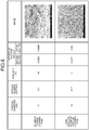
FIG. 6. FIG. 6 is a view illustrating physical properties between the member for a plasma processing device in accordance with the embodiment of the present invention and the member for a plasma processing device in accordance with the comparative example. InFIG. 6 , a porous diameter is an average value of diameters of porous holes and the porous number is the number of porous holes. - As illustrated in
FIG. 6 , it is found that the member for aplasma processing device 1 according to the example either before heating or after heating has a withstand voltage higher than that of the member for a plasma processing device of the comparative example. - The porosity of the member for a
plasma processing device 1 according to the example is lower than that of the member for a plasma processing device of the comparative example, and is within the range described above. - According to the embodiment described above, the
oxide film 20 formed between thebase material 10 and the sprayedfilm 30 has the three-layered configuration of thefirst oxide film 21, thesecond oxide film 22, and thethird oxide film 23, and thefirst oxide film 21 on thebase material 10 side is made harder than the other films (thesecond oxide film 22 and the third oxide film 23), thereby obtaining the member for a plasma processing device having a high withstand voltage. - In this manner, the present invention may include various embodiments and the like that are not described in this specification, and various kinds of design changes and the like can be made without departing from technical ideas specified by the scope of the claims.
- In the embodiment described above, the member for a
plasma processing device 1 that has the sprayedfilm 30 formed on theoxide film 20 has been explained as an example, but the member for a plasma processing device may have the configuration where the sprayedfilm 30 is not included, in other words, may be a member for a plasma processing device formed of thebase material 10 and theoxide film 20. - As described above, the member for a plasma processing device according to the present invention is suitable for implementing a member for a plasma processing device having a high withstand voltage.
-
- 1
- Member for a plasma processing device
- 10
- Base material
- 20
- Oxide film
- 21
- First oxide film
- 21a
- Film layer
- 21b
- Barrier layer
- 22
- Second oxide film
- 23
- Third oxide film
- 30
- Sprayed film
Claims (7)
- A member for a plasma processing device comprising:an aluminum base material; andan oxide film formed on the aluminum base material and having a porous structure, the oxide film includinga first oxide film formed on a surface of the aluminum base material,a second oxide film formed opposite to an aluminum base material side of the first oxide film, anda third oxide film formed opposite to the first oxide film side of the second oxide film,wherein the first oxide film is harder than the second oxide film and the third oxide film, anda hole formed in each of the first oxide film, the second oxide film and the third oxide film is sealed.
- The member for a plasma processing device according to claim 1, further comprising a ceramic sprayed film formed opposite to the aluminum base material side of the oxide film.
- The member for a plasma processing device according to claim 1 or 2, wherein the second oxide film becomes harder from the third oxide film toward the first oxide film.
- The member for a plasma processing device according to any one of claims 1 to 3, wherein the oxide film has porosity of 1% to 2%.
- The member for a plasma processing device according to any one of claims 1 to 4, wherein the first oxide film includes a barrier layer on a part that contacts the aluminum base material, and
the barrier layer has thickness of 80 nm to 210 nm. - The member for a plasma processing device according to any one of claims 1 to 5, wherein
the oxide film is sealed by hydrated alumina, and
the hydrated alumina is hydrate of 1.4 to 2.0. - The member for a plasma processing device according to any one of claims 1 to 6, wherein the oxide film has the thickness of 70 µm to 130 µm.
Applications Claiming Priority (2)
| Application Number | Priority Date | Filing Date | Title |
|---|---|---|---|
| JP2018135083 | 2018-07-18 | ||
| PCT/JP2019/028164 WO2020017566A1 (en) | 2018-07-18 | 2019-07-17 | Member for plasma processing device |
Publications (2)
| Publication Number | Publication Date |
|---|---|
| EP3826435A1 true EP3826435A1 (en) | 2021-05-26 |
| EP3826435A4 EP3826435A4 (en) | 2022-03-16 |
Family
ID=69163829
Family Applications (1)
| Application Number | Title | Priority Date | Filing Date |
|---|---|---|---|
| EP19838458.8A Pending EP3826435A4 (en) | 2018-07-18 | 2019-07-17 | ELEMENT FOR PLASMA TREATMENT DEVICE |
Country Status (7)
| Country | Link |
|---|---|
| US (1) | US12247296B2 (en) |
| EP (1) | EP3826435A4 (en) |
| JP (2) | JP7346412B2 (en) |
| KR (1) | KR102459750B1 (en) |
| CN (1) | CN112514540B (en) |
| TW (1) | TWI741320B (en) |
| WO (1) | WO2020017566A1 (en) |
Cited By (1)
| Publication number | Priority date | Publication date | Assignee | Title |
|---|---|---|---|---|
| WO2024107741A1 (en) * | 2022-11-16 | 2024-05-23 | Applied Materials, Inc. | Porous chamber component coating augmented with colloids |
Families Citing this family (3)
| Publication number | Priority date | Publication date | Assignee | Title |
|---|---|---|---|---|
| JP7801157B2 (en) * | 2022-03-23 | 2026-01-16 | 日本特殊陶業株式会社 | Covering structure and retention device |
| KR20240012676A (en) * | 2022-07-21 | 2024-01-30 | 삼성전자주식회사 | Plasma-resistant member having stacked structure and method for fabricating the same |
| WO2026069493A1 (en) * | 2024-09-25 | 2026-04-02 | 株式会社日立ハイテク | Film formation method, member manufacturing method, and plasma processing apparatus comprising member |
Family Cites Families (13)
| Publication number | Priority date | Publication date | Assignee | Title |
|---|---|---|---|---|
| JPH11229185A (en) * | 1998-02-13 | 1999-08-24 | Kobe Steel Ltd | Aluminum material excellent in resistance to heat cracking and corrosion |
| JP2000114189A (en) | 1998-10-06 | 2000-04-21 | Toshiba Corp | Vacuum processing equipment |
| JP4430266B2 (en) | 2001-05-25 | 2010-03-10 | 東京エレクトロン株式会社 | Plasma processing vessel inner member and plasma processing apparatus |
| US7780786B2 (en) | 2002-11-28 | 2010-08-24 | Tokyo Electron Limited | Internal member of a plasma processing vessel |
| JP2004225113A (en) | 2003-01-23 | 2004-08-12 | Kobe Steel Ltd | Al alloy member excellent in corrosion resistance and plasma resistance |
| JP4486372B2 (en) * | 2003-02-07 | 2010-06-23 | 東京エレクトロン株式会社 | Plasma processing equipment |
| CN100418187C (en) | 2003-02-07 | 2008-09-10 | 东京毅力科创株式会社 | Plasma processing apparatus, annular component and plasma processing method |
| JP4327177B2 (en) | 2006-05-31 | 2009-09-09 | トーカロ株式会社 | Corrosion-resistant thermal spray coating and method of sealing coating of thermal spray coating |
| SG155111A1 (en) | 2008-02-26 | 2009-09-30 | Kobe Steel Ltd | Surface treatment material for semiconductor manufacturing system and method for producing same |
| TW201111557A (en) * | 2009-09-28 | 2011-04-01 | Hong Chang Nano Material Tech Company Ltd | Plasma multilayered aluminum oxide thin film and forming method thereof |
| CN104114752B (en) | 2012-02-12 | 2016-10-12 | 株式会社Uacj | Surface treated aluminum material and manufacture method thereof and the surface treated aluminum material of coated with resin |
| CN103794458B (en) | 2012-10-29 | 2016-12-21 | 中微半导体设备(上海)有限公司 | For the parts within plasma process chamber and manufacture method |
| JP2016065302A (en) | 2014-09-17 | 2016-04-28 | 東京エレクトロン株式会社 | Component for plasma treatment apparatus and manufacturing method of the component |
-
2019
- 2019-07-11 TW TW108124465A patent/TWI741320B/en active
- 2019-07-17 EP EP19838458.8A patent/EP3826435A4/en active Pending
- 2019-07-17 CN CN201980047802.9A patent/CN112514540B/en active Active
- 2019-07-17 US US17/259,609 patent/US12247296B2/en active Active
- 2019-07-17 JP JP2020531348A patent/JP7346412B2/en active Active
- 2019-07-17 WO PCT/JP2019/028164 patent/WO2020017566A1/en not_active Ceased
- 2019-07-17 KR KR1020217001606A patent/KR102459750B1/en active Active
-
2023
- 2023-07-18 JP JP2023117097A patent/JP7682230B2/en active Active
Cited By (1)
| Publication number | Priority date | Publication date | Assignee | Title |
|---|---|---|---|---|
| WO2024107741A1 (en) * | 2022-11-16 | 2024-05-23 | Applied Materials, Inc. | Porous chamber component coating augmented with colloids |
Also Published As
| Publication number | Publication date |
|---|---|
| JP7346412B2 (en) | 2023-09-19 |
| KR102459750B1 (en) | 2022-10-26 |
| US12247296B2 (en) | 2025-03-11 |
| JPWO2020017566A1 (en) | 2021-08-26 |
| CN112514540B (en) | 2024-06-07 |
| KR20210021065A (en) | 2021-02-24 |
| TW202007233A (en) | 2020-02-01 |
| JP7682230B2 (en) | 2025-05-23 |
| WO2020017566A1 (en) | 2020-01-23 |
| US20210292911A1 (en) | 2021-09-23 |
| JP2023126546A (en) | 2023-09-07 |
| TWI741320B (en) | 2021-10-01 |
| CN112514540A (en) | 2021-03-16 |
| EP3826435A4 (en) | 2022-03-16 |
Similar Documents
| Publication | Publication Date | Title |
|---|---|---|
| US12247296B2 (en) | Member for plasma processing device | |
| TWI463597B (en) | High efficiency electrostatic chuck assembly for semiconductor wafer processing | |
| CN101689429B (en) | Electrode foil, manufacturing method thereof, and electrolytic capacitor | |
| CN107592941B (en) | Plasma-resistant coating film and method for forming same | |
| JP4272786B2 (en) | Electrostatic chuck member and manufacturing method thereof | |
| US20220345054A1 (en) | Electrostatic adsorption member and substrate fixing device | |
| US8739732B2 (en) | Plasma treatment container internal member, and plasma treatment apparatus having the plasma treatment container internal member | |
| US20200234879A1 (en) | Multi-layer ceramic capacitor and method of producing the same | |
| US8237333B2 (en) | Piezoelectric actuator and method for producing a piezoelectric actuator | |
| KR102335537B1 (en) | Thin foil and manufacturing method for thin foil | |
| JP2022501821A (en) | Dielectric structure for electrical insulation by vacuum or gas | |
| CN109156080B (en) | Ceramic electronic parts | |
| KR101115527B1 (en) | Electrostatic Chuck | |
| WO2010058552A1 (en) | Electrode body for capacitor and capacitor | |
| CN114946000B (en) | Electrolytic capacitor and method for manufacturing electrolytic capacitor | |
| JP7143674B2 (en) | metallized film and film capacitors | |
| CN1278389C (en) | Plasma processing apparatus and manufacturing method of electrostatic chuck | |
| KR101355505B1 (en) | Electro static chuck and method for electro static chuck | |
| US20260028710A1 (en) | Method of manufacturing plasma-resistant multilayer coating film | |
| TW202346099A (en) | Laminates and electrostatic chuck devices | |
| KR101192967B1 (en) | Electrostatic chuck for manufacturing LCD | |
| WO2026043917A1 (en) | Substrate coating for high voltage applications | |
| TW202422592A (en) | Insulated wire | |
| KR20160091469A (en) | Dc port for high voltage electro static chuck | |
| Choi et al. | Fabrication and characterization of multi-layered ceramic ion generators based on dielectric barrier discharge |
Legal Events
| Date | Code | Title | Description |
|---|---|---|---|
| STAA | Information on the status of an ep patent application or granted ep patent |
Free format text: STATUS: THE INTERNATIONAL PUBLICATION HAS BEEN MADE |
|
| PUAI | Public reference made under article 153(3) epc to a published international application that has entered the european phase |
Free format text: ORIGINAL CODE: 0009012 |
|
| STAA | Information on the status of an ep patent application or granted ep patent |
Free format text: STATUS: REQUEST FOR EXAMINATION WAS MADE |
|
| 17P | Request for examination filed |
Effective date: 20210113 |
|
| AK | Designated contracting states |
Kind code of ref document: A1 Designated state(s): AL AT BE BG CH CY CZ DE DK EE ES FI FR GB GR HR HU IE IS IT LI LT LU LV MC MK MT NL NO PL PT RO RS SE SI SK SM TR |
|
| DAV | Request for validation of the european patent (deleted) | ||
| DAX | Request for extension of the european patent (deleted) | ||
| A4 | Supplementary search report drawn up and despatched |
Effective date: 20220216 |
|
| RIC1 | Information provided on ipc code assigned before grant |
Ipc: C25D 11/24 20060101ALI20220210BHEP Ipc: C23C 4/10 20160101ALI20220210BHEP Ipc: H01J 37/32 20060101ALI20220210BHEP Ipc: C25D 11/00 20060101ALI20220210BHEP Ipc: H01L 21/3065 20060101ALI20220210BHEP Ipc: C25D 11/18 20060101ALI20220210BHEP Ipc: C25D 11/12 20060101ALI20220210BHEP Ipc: C25D 11/04 20060101ALI20220210BHEP Ipc: C23C 28/04 20060101ALI20220210BHEP Ipc: H05H 1/24 20060101AFI20220210BHEP |
|
| STAA | Information on the status of an ep patent application or granted ep patent |
Free format text: STATUS: EXAMINATION IS IN PROGRESS |
|
| 17Q | First examination report despatched |
Effective date: 20251201 |