EP3826175A1 - High-linearity amplifier - Google Patents
High-linearity amplifier Download PDFInfo
- Publication number
- EP3826175A1 EP3826175A1 EP20205039.9A EP20205039A EP3826175A1 EP 3826175 A1 EP3826175 A1 EP 3826175A1 EP 20205039 A EP20205039 A EP 20205039A EP 3826175 A1 EP3826175 A1 EP 3826175A1
- Authority
- EP
- European Patent Office
- Prior art keywords
- amplifier
- resistor
- operational amplifier
- compensation
- main operational
- Prior art date
- Legal status (The legal status is an assumption and is not a legal conclusion. Google has not performed a legal analysis and makes no representation as to the accuracy of the status listed.)
- Withdrawn
Links
Images




Classifications
-
- H—ELECTRICITY
- H03—ELECTRONIC CIRCUITRY
- H03F—AMPLIFIERS
- H03F3/00—Amplifiers with only discharge tubes or only semiconductor devices as amplifying elements
- H03F3/45—Differential amplifiers
- H03F3/45071—Differential amplifiers with semiconductor devices only
- H03F3/45076—Differential amplifiers with semiconductor devices only characterised by the way of implementation of the active amplifying circuit in the differential amplifier
- H03F3/45475—Differential amplifiers with semiconductor devices only characterised by the way of implementation of the active amplifying circuit in the differential amplifier using IC blocks as the active amplifying circuit
-
- H—ELECTRICITY
- H03—ELECTRONIC CIRCUITRY
- H03F—AMPLIFIERS
- H03F1/00—Details of amplifiers with only discharge tubes, only semiconductor devices or only unspecified devices as amplifying elements
- H03F1/34—Negative-feedback-circuit arrangements with or without positive feedback
-
- H—ELECTRICITY
- H03—ELECTRONIC CIRCUITRY
- H03F—AMPLIFIERS
- H03F1/00—Details of amplifiers with only discharge tubes, only semiconductor devices or only unspecified devices as amplifying elements
- H03F1/08—Modifications of amplifiers to reduce detrimental influences of internal impedances of amplifying elements
- H03F1/083—Modifications of amplifiers to reduce detrimental influences of internal impedances of amplifying elements in transistor amplifiers
-
- H—ELECTRICITY
- H03—ELECTRONIC CIRCUITRY
- H03F—AMPLIFIERS
- H03F1/00—Details of amplifiers with only discharge tubes, only semiconductor devices or only unspecified devices as amplifying elements
- H03F1/32—Modifications of amplifiers to reduce non-linear distortion
- H03F1/3211—Modifications of amplifiers to reduce non-linear distortion in differential amplifiers
-
- H—ELECTRICITY
- H03—ELECTRONIC CIRCUITRY
- H03F—AMPLIFIERS
- H03F3/00—Amplifiers with only discharge tubes or only semiconductor devices as amplifying elements
- H03F3/45—Differential amplifiers
-
- H—ELECTRICITY
- H03—ELECTRONIC CIRCUITRY
- H03F—AMPLIFIERS
- H03F2203/00—Indexing scheme relating to amplifiers with only discharge tubes or only semiconductor devices as amplifying elements covered by H03F3/00
- H03F2203/45—Indexing scheme relating to differential amplifiers
- H03F2203/45528—Indexing scheme relating to differential amplifiers the FBC comprising one or more passive resistors and being coupled between the LC and the IC
-
- H—ELECTRICITY
- H03—ELECTRONIC CIRCUITRY
- H03F—AMPLIFIERS
- H03F2203/00—Indexing scheme relating to amplifiers with only discharge tubes or only semiconductor devices as amplifying elements covered by H03F3/00
- H03F2203/45—Indexing scheme relating to differential amplifiers
- H03F2203/45601—Indexing scheme relating to differential amplifiers the IC comprising one or more passive resistors by feedback
Definitions
- the present invention relates to operational amplifiers.
- Operational amplifiers are among the most widely used electronic devices today, being used in a vast array of consumer, industrial, and scientific devices.
- a headphone amplifier may be implemented using an operational amplifier.
- FIG. 1 depicts a conventional amplifier 100 implemented by an operational amplifier op_amp. Due to the velocity saturation effect, the resistance of the feedback resistor Rf is seriously affected (e.g., 2nd-order voltage coefficient in the resistance of the feedback resistor Rf) by a large voltage swing across the feedback resistor Rf, which results in serious odd harmonics (e.g., HD3, HD5, HD7, and so on) in the amplification.
- odd harmonics e.g., HD3, HD5, HD7, and so on
- One conventional solution is to use a large-sized feedback resistor Rf to sustain the large voltage swing.
- the improvement is not efficient.
- the width of the feedback resistor Rf is increased by 2 N times, the third-order harmonic HD3 is only improved by N ⁇ 12dB.
- Targeted at -130dBc third-order harmonic (HD3), the feedback resistor Rf is too huge in size.
- the circuit size of the entire amplifier is very large.
- An amplifier in accordance with an exemplary embodiment of the present invention includes a main operational amplifier, a feedback circuit, and a compensation circuit.
- the feedback circuit couples an output signal of the main operational amplifier to an input port of the main operational amplifier.
- the compensation circuit is coupled to the input port of the main operational amplifier to compensate for the non-linearity of the feedback circuit. Specifically, a signal coupled to the input port of the main operational amplifier through the compensation circuit has an inverse phase compared to the output signal of the main operational amplifier.
- the amplifier is a fully-differential amplifier.
- the main operational amplifier has a non-inverting input terminal, an inverting input terminal, a positive output terminal, and a negative output terminal.
- the feedback circuit includes a first feedback resistor coupled between the positive output terminal and the inverting input terminal of the main operational amplifier, and a second feedback resistor coupled between the negative output terminal and the non-inverting input terminal of the main operational amplifier.
- the compensation circuit includes a first compensation resistor coupled between the negative output terminal and the inverting input terminal of the main operational amplifier, and a second compensation resistor coupled between the positive output terminal and the non-inverting input terminal of the main operational amplifier. The compensation circuit provides a positive feedback path for the amplification.
- the compensation circuit provides a feed-forward path to compensate for the non-linearity of the feedback circuit.
- the non-inverting input terminal of the main operational amplifier is coupled to a positive output terminal of a former-stage circuit of the amplifier, and the inverting input terminal of the main operational amplifier is coupled to a negative output terminal of the former-stage circuit of the amplifier.
- the compensation circuit includes a first compensation resistor coupled between the positive output terminal of the former-stage circuit of the amplifier and the inverting input terminal of the main operational amplifier, and a second compensation resistor coupled between the negative output terminal of the former-stage circuit of the amplifier and the non-inverting input terminal of the main operational amplifier.
- the resistance of the first compensation resistor is greater than the resistance of the first feedback resistor, and the resistance of the second compensation resistor is greater than the resistance of the second feedback resistor.
- the size of the first compensation resistor is smaller than the size of the first feedback resistor, and the size of the second compensation resistor is smaller than the size of the second feedback resistor.
- the resistance of the first compensation resistor is N times the resistance of the first feedback resistor, and N is greater than 1.
- the length and width of the first feedback resistor are L1 and W1, respectively.
- the length and width of the first compensation resistor are L2 and W2, respectively.
- L2 is L 1 / N and W2 is W 1 / N • N .
- Size of the second feedback resistor may equal size of the first feedback resistor.
- Size of the second compensation resistor may equal size of the first compensation resistor.
- the amplifier is implemented as a single-ended amplifier.
- FIG. 2A and FIG. 2B depict a solution to the non-linearity of the feedback resistor Rf of FIG. 1 .
- An inverse paralleling linearization architecture is introduced.
- FIG. 2A the voltage Vop across the feedback resistor Rf is inverted by an inverting amplification circuit inv_amp (with an amplitude gain 1) and thereby the voltage across a compensation resistor Rc is in an inverse phase (Vop) compared to the voltage (+Vop) across the feedback resistor Rf.
- Such architecture is named the inverse paralleling linearization.
- FIG. 2B shows the current-voltage (I-V) plot of the resistors of FIG. 2B .
- the I-V plot of the feedback resistor Rf is 202, which contains a 2nd-order degradation, e.g., Rf(1-a (2, Rf) Vop 2 ), where a (2, Rf) is the 2nd-order non-linearity voltage coefficient of the feedback resistor Rf.
- the I-V plot of the compensation resistor Rc is 204, whose 2nd-order harmonic is in another direction, e.g., Rc(1+a (2, Rc) Vop 2 ), where a (2, Rc) is the 2nd-order non-linearity voltage coefficient of the compensation resistor Rc.
- the I-V plot of the equivalent resistance is 206, which approaches the ideal feedback resistor Rf.
- the inverse paralleling linearization architecture may be implemented in a positive feedback loop path of an amplifier.
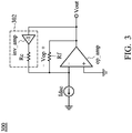
- FIG. 3 depicts a single-ended amplifier 300 with the inverse paralleling linearization in a positive feedback loop path.
- the single-ended amplifier 300 has a main operational amplifier op_amp, a feedback resistor Rf, and a compensation circuit 302 including a compensation resistor Rc and an inverting amplification circuit inv_amp (with an amplitude gain 1).
- the main operational amplifier op_amp has a non-inverting input terminal '+', an inverting input terminal '-', and a single-ended output terminal outputting the amplified signal Vout.
- the feedback resistor Rf is coupled between the single-ended output terminal (Vout) and the inverting input terminal '-' of the main operational amplifier op_amp.
- the compensation circuit 302 is provided in the positive feedback loop path of the single-ended amplifier 300 to form an inverse paralleling linearization architecture with the feedback resistor Rf.
- non-linearity of the feedback resistor Rf is compensated by the compensation circuit 302.
- the single-ended output terminal (Vout) of the main operational amplifier op_amp is coupled to an input terminal of the inverting amplification circuit inv_amp
- an output terminal of the inverting amplification circuit inv_amp is coupled to the inverting terminal '-' of the main operational amplifier op_amp through the compensation resistor Rc.
- the single-ended amplifier 300 is an I-V amplifier, whose input signal is a current signal Idac and output signal is a voltage signal Vout.
- V-V amplification can also use the compensation circuit 302.
- the resistance of the compensation resistor Rc is greater than
- the resistance of the compensation resistor Rc is N times the resistance of the feedback resistor Rf, and N is greater than 1.
- the length and width of the feedback resistor Rf are L1 and W1, respectively.
- the length and width of the compensation resistor Rc are L2 and W2, respectively.
- the size of the compensation resistor Rc is smaller than the size of the feedback resistor Rf.
- the single-ended amplifier 300 is a reasonable-sized amplifier with high-linearity.
- N is greater than 10.
- N may be 29.
- W1 is 32 ⁇ and L1 is 189 ⁇
- W2 is 0.2 ⁇
- L2 is 35.1 ⁇ .
- Both feedback resistor Rf and the compensation resistor Rc are small-sized resistors.
- the inverting amplification circuit inv_amp of the compensation circuit 302 may have a magnitude gain k greater than 1.
- the resistance of the compensation resistor Rc is k ⁇ N times the resistance of the feedback resistor Rf, and N is greater than 1.
- the size of the compensation resistor Rc is further shrunk by k.
- N 29
- W1 32 ⁇
- L1 189 ⁇
- k 248 ⁇
- the size of compensation resistor Rc is smaller than the forgoing example.
- the feedback resistor Rf is also manufactured in a small size.
- the feedback resistor Rf may be implemented by multiple small-sized resistors which are coupled in parallel.
- FIG. 4 depicts a fully-differential amplifier 400 with the inverse paralleling linearization in a positive feedback loop path.
- the fully-differential amplifier 400 has a main operational amplifier op_amp, a feedback circuit including a first feedback resistor Rf1 and a second resistor Rf2, and a compensation circuit including a first compensation resistor Rc1 and a second compensation resistor Rc2.
- the main operational amplifier op_amp has a non-inverting input terminal '+', an inverting input terminal '-', a positive output terminal (Vout_p), and a negative output terminal (Vout_n).
- the amplified signal is (Vout_p - Vout_n).
- the first feedback resistor Rf1 is coupled between the positive output terminal (Vout_p) and the inverting input terminal '-' of the main operational amplifier op_amp
- the second feedback resistor Rf2 is coupled between the negative output terminal (Vout_n) and the non-inverting input terminal '+' of the main operational amplifier op_amp
- the first compensation resistor Rc1 is coupled between the negative output terminal (Vout_n) and the inverting input terminal '-' of the main operational amplifier op_amp
- the second compensation resistor Rc2 is coupled between the positive output terminal (Vout_p) and the non-inverting input terminal '+' of the main operational amplifier op_amp. Inverse paralleling linearization is successfully performed on both the first and second feedback resistors Rf1 and Rf2
- the resistance of the first compensation resistor Rc1 is greater than the resistance of the first feedback resistor Rf1
- the size of the first compensation resistor Rc1 is smaller than the size of the first feedback resistor Rf1
- the resistance of the second compensation resistor Rc2 is greater than the resistance of the second feedback resistor Rf2
- the size of the second compensation resistor Rc2 is smaller than the size of the second feedback resistor Rf2.
- the resistance of the first compensation resistor Rc1 is N times the resistance of the first feedback resistor Rf1, and N is greater than 1.
- the length and width of the first feedback resistor Rf1 are L1 and W1, respectively.
- the length and width of the first compensation resistor Rc1 are L2 and W2, respectively.
- L2 is L 1 / N and W2 is W 1 / N • N .
- the size of the second feedback resistor Rf2 may be equal the size of the first feedback resistor Rf1.
- the size of the second compensation resistor Rc2 may be equal the size of the first compensation resistor Rc1.
- the feedback resistors Rf1 and Rf2 are also manufactured in a small size.
- the feedback resistor Rf1/Rf2 may be implemented by multiple small-sized resistors which are coupled in parallel.
- the inverse paralleling linearization architecture may be implemented in a feed-forward signal path rather than based on feedback of the amplifier.
- FIG. 5 depicts a single-ended amplifier 500 with the inverse paralleling linearization in a feed-forward signal path.
- the compensation circuit 502 of the single-ended amplifier 500 is coupled between a former-stage circuit of the single-ended amplifier 500 and the inverting input terminal '-' of the main operational amplifier op_amp.
- the former-stage circuit provides the single-ended amplifier 500 with a current signal Idac as an input signal of the single-ended amplifier 500.
- the compensation circuit 502 further has a converter 504 that converts the input signal Idac of the single-ended amplifier 500 to an inverted signal compared to the output signal Vout of the single-ended amplifier 500.
- the resistance of the compensation resistor Rc is greater than the resistance of the feedback resistor Rf, and the size of the compensation resistor Rc is smaller than the size of the feedback resistor Rf.
- the resistance of the compensation resistor Rc is N times the resistance of the feedback resistor Rf, and N is greater than 1.
- the length and width of the feedback resistor Rf are L1 and W1, respectively.
- the length and width of the compensation resistor Rc are L2 and W2, respectively.
- L2 is L 1 / N and W2 is W1/(N• N ).
- the converter 504 further includes an amplification circuit with a gain, k, greater than 1.
- the resistance of the compensation resistor Rc is k ⁇ N times the resistance of the feedback resistor Rf, and N is greater than 1.
- the size of the compensation resistor Rc is further shrunk by k.
- the feedback resistor Rf is also manufactured in a small size.
- the feedback resistor Rf may be implemented by multiple small-sized resistors which are coupled in parallel.
- FIG. 6 depicts a fully-differential amplifier 600 with the inverse paralleling linearization in a feed-forward signal path.
- the first compensation resistor Rc1 is coupled between a positive output terminal FS_p of a former-stage circuit 602 of the fully-differential amplifier 600 and the inverting input terminal '-' of the main operational amplifier op_amp
- a second compensation resistor Rc2 is coupled between a negative output terminal FS_n of the former-stage circuit 602 of the fully-differential amplifier 600 and the non-inverting input terminal '+' of the main operational amplifier op_amp.
- the former-stage circuit 602 uses the positive and negative output terminals FS_p and FS_n to transfer a voltage signal into the fully-differential amplifier 600 as the input signal of the fully-differential amplifier 600.
- inverse paralleling linearization is successfully performed in a feed-forward signal path.
- the resistance of the first compensation resistor Rc1 is greater than the resistance of the first feedback resistor Rf1
- the size of the first compensation resistor Rc1 is smaller than the size of the first feedback resistor Rf1
- the resistance of the second compensation resistor Rc2 is greater than the resistance of the second feedback resistor Rf2
- the size of the second compensation resistor Rc2 is smaller than the size of the second feedback resistor Rf2.
- the resistance of the first compensation resistor Rc1 is N times the resistance of the first feedback resistor Rf1, and N is greater than 1.
- the length and width of the first feedback resistor Rf1 are L1 and W1, respectively.
- the length and width of the first compensation resistor Rc1 are L2 and W2, respectively.
- L2 is L 1 / N and W2 is W 1 / N • N .
- the size of the second feedback resistor Rf2 may equal the size of the first feedback resistor Rf1.
- the size of the second compensation resistor Rc2 may equal the size of the first compensation resistor Rc1.
- the feedback resistors Rf1 and Rf2 are also manufactured in a small size.
- the feedback resistor Rf1/Rf2 may be implemented by multiple small-sized resistors which are coupled in parallel.
- Any amplifier with a compensation circuit coupled to the input port of the main operational amplifier to compensate for the non-linearity of the feedback circuit should be considered within the scope with the present invention.
- a signal coupled to the input port of the main operational amplifier through the compensation circuit has an inverse phase compared to the output signal of the main operational amplifier.
Landscapes
- Engineering & Computer Science (AREA)
- Power Engineering (AREA)
- Physics & Mathematics (AREA)
- Nonlinear Science (AREA)
- Amplifiers (AREA)
Abstract
Description
- The present invention relates to operational amplifiers.
- Operational amplifiers (op amps) are among the most widely used electronic devices today, being used in a vast array of consumer, industrial, and scientific devices. For example, a headphone amplifier may be implemented using an operational amplifier.
-
FIG. 1 depicts aconventional amplifier 100 implemented by an operational amplifier op_amp. Due to the velocity saturation effect, the resistance of the feedback resistor Rf is seriously affected (e.g., 2nd-order voltage coefficient in the resistance of the feedback resistor Rf) by a large voltage swing across the feedback resistor Rf, which results in serious odd harmonics (e.g., HD3, HD5, HD7, and so on) in the amplification. - One conventional solution is to use a large-sized feedback resistor Rf to sustain the large voltage swing. However, the improvement is not efficient. The width of the feedback resistor Rf is increased by 2N times, the third-order harmonic HD3 is only improved by N∗12dB. Targeted at -130dBc third-order harmonic (HD3), the feedback resistor Rf is too huge in size. The circuit size of the entire amplifier is very large.
- A reasonable-sized amplifier with high-linearity is introduced.
- An amplifier in accordance with an exemplary embodiment of the present invention includes a main operational amplifier, a feedback circuit, and a compensation circuit. The feedback circuit couples an output signal of the main operational amplifier to an input port of the main operational amplifier. The compensation circuit is coupled to the input port of the main operational amplifier to compensate for the non-linearity of the feedback circuit. Specifically, a signal coupled to the input port of the main operational amplifier through the compensation circuit has an inverse phase compared to the output signal of the main operational amplifier.
- In an exemplary embodiment, the amplifier is a fully-differential amplifier. The main operational amplifier has a non-inverting input terminal, an inverting input terminal, a positive output terminal, and a negative output terminal. The feedback circuit includes a first feedback resistor coupled between the positive output terminal and the inverting input terminal of the main operational amplifier, and a second feedback resistor coupled between the negative output terminal and the non-inverting input terminal of the main operational amplifier. The compensation circuit includes a first compensation resistor coupled between the negative output terminal and the inverting input terminal of the main operational amplifier, and a second compensation resistor coupled between the positive output terminal and the non-inverting input terminal of the main operational amplifier. The compensation circuit provides a positive feedback path for the amplification.
- In another exemplary embodiment, the compensation circuit provides a feed-forward path to compensate for the non-linearity of the feedback circuit. The non-inverting input terminal of the main operational amplifier is coupled to a positive output terminal of a former-stage circuit of the amplifier, and the inverting input terminal of the main operational amplifier is coupled to a negative output terminal of the former-stage circuit of the amplifier. The compensation circuit includes a first compensation resistor coupled between the positive output terminal of the former-stage circuit of the amplifier and the inverting input terminal of the main operational amplifier, and a second compensation resistor coupled between the negative output terminal of the former-stage circuit of the amplifier and the non-inverting input terminal of the main operational amplifier.
- In the forgoing fully-differential architecture, the resistance of the first compensation resistor is greater than the resistance of the first feedback resistor, and the resistance of the second compensation resistor is greater than the resistance of the second feedback resistor. In some exemplary embodiments, the size of the first compensation resistor is smaller than the size of the first feedback resistor, and the size of the second compensation resistor is smaller than the size of the second feedback resistor.
- In an exemplary embodiment, the resistance of the first compensation resistor is N times the resistance of the first feedback resistor, and N is greater than 1. The length and width of the first feedback resistor are L1 and W1, respectively. The length and width of the first compensation resistor are L2 and W2, respectively. L2 is


- In some exemplary embodiments, the amplifier is implemented as a single-ended amplifier.
- A detailed description is given in the following embodiments with reference to the accompanying drawings.
- The present invention can be more fully understood by reading the subsequent detailed description and examples with references made to the accompanying drawings, wherein:
-
FIG. 1 depicts aconventional amplifier 100 implemented by an operational amplifier op_amp; -
FIG. 2A and FIG. 2B depict a solution to the non-linearity of the feedback resistor Rf ofFIG. 1 , wherein an inverse paralleling linearization architecture is introduced; -
FIG. 3 depicts a single-ended amplifier 300 with the inverse paralleling linearization in a positive feedback loop path; -
FIG. 4 depicts a fully-differential amplifier 400 with the inverse paralleling linearization in a positive feedback loop path; -
FIG. 5 depicts a single-ended amplifier 500 with the inverse paralleling linearization in a feed-forward signal path; and -
FIG. 6 depicts a fully-differential amplifier 600 with the inverse paralleling linearization in a feed-forward signal path. - The following description shows exemplary embodiments carrying out the invention. This description is made for the purpose of illustrating the general principles of the invention and should not be taken in a limiting sense. The scope of the invention is best determined by reference to the appended claims.
-
FIG. 2A and FIG. 2B depict a solution to the non-linearity of the feedback resistor Rf ofFIG. 1 . An inverse paralleling linearization architecture is introduced. - Referring to
FIG. 2A , the voltage Vop across the feedback resistor Rf is inverted by an inverting amplification circuit inv_amp (with an amplitude gain 1) and thereby the voltage across a compensation resistor Rc is in an inverse phase (Vop) compared to the voltage (+Vop) across the feedback resistor Rf. Such architecture is named the inverse paralleling linearization.FIG. 2B shows the current-voltage (I-V) plot of the resistors ofFIG. 2B . The I-V plot of the feedback resistor Rf is 202, which contains a 2nd-order degradation, e.g., Rf(1-a(2, Rf)Vop2), where a(2, Rf) is the 2nd-order non-linearity voltage coefficient of the feedback resistor Rf. The I-V plot of the compensation resistor Rc is 204, whose 2nd-order harmonic is in another direction, e.g., Rc(1+a(2, Rc)Vop2), where a(2, Rc) is the 2nd-order non-linearity voltage coefficient of the compensation resistor Rc. According to the inverse paralleling linearization architecture ofFIG. 2A , the I-V plot of the equivalent resistance is 206, which approaches the ideal feedback resistor Rf. - The inverse paralleling linearization architecture may be implemented in a positive feedback loop path of an amplifier.
-
FIG. 3 depicts a single-endedamplifier 300 with the inverse paralleling linearization in a positive feedback loop path. - The single-ended
amplifier 300 has a main operational amplifier op_amp, a feedback resistor Rf, and acompensation circuit 302 including a compensation resistor Rc and an inverting amplification circuit inv_amp (with an amplitude gain 1). The main operational amplifier op_amp has a non-inverting input terminal '+', an inverting input terminal '-', and a single-ended output terminal outputting the amplified signal Vout. The feedback resistor Rf is coupled between the single-ended output terminal (Vout) and the inverting input terminal '-' of the main operational amplifier op_amp. Thecompensation circuit 302 is provided in the positive feedback loop path of the single-endedamplifier 300 to form an inverse paralleling linearization architecture with the feedback resistor Rf. Thus, non-linearity of the feedback resistor Rf is compensated by thecompensation circuit 302. As shown, the single-ended output terminal (Vout) of the main operational amplifier op_amp is coupled to an input terminal of the inverting amplification circuit inv_amp, an output terminal of the inverting amplification circuit inv_amp is coupled to the inverting terminal '-' of the main operational amplifier op_amp through the compensation resistor Rc. - The single-ended
amplifier 300 is an I-V amplifier, whose input signal is a current signal Idac and output signal is a voltage signal Vout. In the other exemplary embodiments, V-V amplification can also use thecompensation circuit 302. - In the inverse paralleling linearization architecture, the output signal Vout is:

- In an exemplary embodiment, the resistance of the compensation resistor Rc is N times the resistance of the feedback resistor Rf, and N is greater than 1. The length and width of the feedback resistor Rf are L1 and W1, respectively. The length and width of the compensation resistor Rc are L2 and W2, respectively. Specifically, the design of the compensation resistor Rc is:

amplifier 300 is a reasonable-sized amplifier with high-linearity. - In an exemplary embodiment, to perfectly minimize the noise contribution or instability introduced through the positive feedback loop path, N is greater than 10. For example, N may be 29. When W1 is 32µ and L1 is 189µ, W2 is 0.2µ and L2 is 35.1µ. Both feedback resistor Rf and the compensation resistor Rc are small-sized resistors.
- In another exemplary embodiment, the inverting amplification circuit inv_amp of the
compensation circuit 302 may have a magnitude gain k greater than 1. In such an example, the resistance of the compensation resistor Rc is k∗N times the resistance of the feedback resistor Rf, and N is greater than 1. Specifically, the design of the compensation resistor Rc is:
- The size of the compensation resistor Rc is further shrunk by k. In the example wherein N is 29, W1 is 32µ, L1 is 189µ, and k is 2, W2 is 0.072µ and L2 is 24.8µ. The size of compensation resistor Rc is smaller than the forgoing example.
- In the other exemplary embodiments, the feedback resistor Rf is also manufactured in a small size. For example, the feedback resistor Rf may be implemented by multiple small-sized resistors which are coupled in parallel.
-
FIG. 4 depicts a fully-differential amplifier 400 with the inverse paralleling linearization in a positive feedback loop path. - The fully-
differential amplifier 400 has a main operational amplifier op_amp, a feedback circuit including a first feedback resistor Rf1 and a second resistor Rf2, and a compensation circuit including a first compensation resistor Rc1 and a second compensation resistor Rc2. The main operational amplifier op_amp has a non-inverting input terminal '+', an inverting input terminal '-', a positive output terminal (Vout_p), and a negative output terminal (Vout_n). The amplified signal is (Vout_p - Vout_n). The first feedback resistor Rf1 is coupled between the positive output terminal (Vout_p) and the inverting input terminal '-' of the main operational amplifier op_amp, and the second feedback resistor Rf2 is coupled between the negative output terminal (Vout_n) and the non-inverting input terminal '+' of the main operational amplifier op_amp. The first compensation resistor Rc1 is coupled between the negative output terminal (Vout_n) and the inverting input terminal '-' of the main operational amplifier op_amp, and the second compensation resistor Rc2 is coupled between the positive output terminal (Vout_p) and the non-inverting input terminal '+' of the main operational amplifier op_amp. Inverse paralleling linearization is successfully performed on both the first and second feedback resistors Rf1 and Rf2 - In an exemplary embodiment, the resistance of the first compensation resistor Rc1 is greater than the resistance of the first feedback resistor Rf1, the size of the first compensation resistor Rc1 is smaller than the size of the first feedback resistor Rf1, the resistance of the second compensation resistor Rc2 is greater than the resistance of the second feedback resistor Rf2, and the size of the second compensation resistor Rc2 is smaller than the size of the second feedback resistor Rf2.
- In an exemplary embodiment, the resistance of the first compensation resistor Rc1 is N times the resistance of the first feedback resistor Rf1, and N is greater than 1. The length and width of the first feedback resistor Rf1 are L1 and W1, respectively. The length and width of the first compensation resistor Rc1 are L2 and W2, respectively. L2 is


- In the other exemplary embodiments, the feedback resistors Rf1 and Rf2 are also manufactured in a small size. For example, the feedback resistor Rf1/Rf2 may be implemented by multiple small-sized resistors which are coupled in parallel.
- In some exemplary embodiments, the inverse paralleling linearization architecture may be implemented in a feed-forward signal path rather than based on feedback of the amplifier.
-
FIG. 5 depicts a single-endedamplifier 500 with the inverse paralleling linearization in a feed-forward signal path. In comparison with the single-endedamplifier 300 ofFIG. 3 , thecompensation circuit 502 of the single-endedamplifier 500 is coupled between a former-stage circuit of the single-endedamplifier 500 and the inverting input terminal '-' of the main operational amplifier op_amp. - In an exemplary embodiment, the former-stage circuit provides the single-ended
amplifier 500 with a current signal Idac as an input signal of the single-endedamplifier 500. In addition to the compensation resistor Rc, thecompensation circuit 502 further has aconverter 504 that converts the input signal Idac of the single-endedamplifier 500 to an inverted signal compared to the output signal Vout of the single-endedamplifier 500. In an exemplary embodiment, theconverter 504 generates a voltage (≈-Iout∗Rf=-Vout) to be coupled to the inverting input terminal '-' of the main operational amplifier op_amp through the compensation circuit Rc. - In this structure shown in
FIG. 5 , inverse paralleling linearization is successfully performed in a feed-forward signal path. The resistance of the compensation resistor Rc is greater than the resistance of the feedback resistor Rf, and the size of the compensation resistor Rc is smaller than the size of the feedback resistor Rf. In an exemplary embodiment, the resistance of the compensation resistor Rc is N times the resistance of the feedback resistor Rf, and N is greater than 1. The length and width of the feedback resistor Rf are L1 and W1, respectively. The length and width of the compensation resistor Rc are L2 and W2, respectively. L2 is

- In another exemplary embodiment, the
converter 504 further includes an amplification circuit with a gain, k, greater than 1. The inverted signal (≈-Iout∗Rf=-Vout) is amplified k times and then coupled to the inverting input terminal '-' of the main operational amplifier op_amp through the compensation circuit Rc. In such an example, the resistance of the compensation resistor Rc is k∗N times the resistance of the feedback resistor Rf, and N is greater than 1. Specifically, the design of the compensation resistor Rc is: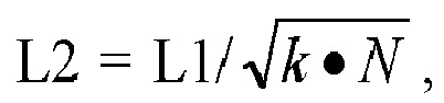

- In the other exemplary embodiments, the feedback resistor Rf is also manufactured in a small size. For example, the feedback resistor Rf may be implemented by multiple small-sized resistors which are coupled in parallel.
-
FIG. 6 depicts a fully-differential amplifier 600 with the inverse paralleling linearization in a feed-forward signal path. In comparison with the single-endedamplifier 400 ofFIG. 4 , the first compensation resistor Rc1 is coupled between a positive output terminal FS_p of a former-stage circuit 602 of the fully-differential amplifier 600 and the inverting input terminal '-' of the main operational amplifier op_amp, and a second compensation resistor Rc2 is coupled between a negative output terminal FS_n of the former-stage circuit 602 of the fully-differential amplifier 600 and the non-inverting input terminal '+' of the main operational amplifier op_amp. The former-stage circuit 602 uses the positive and negative output terminals FS_p and FS_n to transfer a voltage signal into the fully-differential amplifier 600 as the input signal of the fully-differential amplifier 600. There is a first input resistor Rin1 coupled between the positive output terminal FS_p of the former-stage circuit 602 and the non-inverting input terminal '+' of the main operational amplifier op_amp, and a second input resistor Rin2 coupled between the negative output terminal FS_n of the former-stage circuit 602 and the inverting input terminal '-' of the main operational amplifier op_amp. - In this structure shown in
FIG. 6 , inverse paralleling linearization is successfully performed in a feed-forward signal path. The resistance of the first compensation resistor Rc1 is greater than the resistance of the first feedback resistor Rf1, the size of the first compensation resistor Rc1 is smaller than the size of the first feedback resistor Rf1, the resistance of the second compensation resistor Rc2 is greater than the resistance of the second feedback resistor Rf2, and the size of the second compensation resistor Rc2 is smaller than the size of the second feedback resistor Rf2. - In an exemplary embodiment, the resistance of the first compensation resistor Rc1 is N times the resistance of the first feedback resistor Rf1, and N is greater than 1. The length and width of the first feedback resistor Rf1 are L1 and W1, respectively. The length and width of the first compensation resistor Rc1 are L2 and W2, respectively. L2 is


- In the other exemplary embodiments, the feedback resistors Rf1 and Rf2 are also manufactured in a small size. For example, the feedback resistor Rf1/Rf2 may be implemented by multiple small-sized resistors which are coupled in parallel.
- There may be various modifications of the amplifier architecture. Any amplifier with a compensation circuit coupled to the input port of the main operational amplifier to compensate for the non-linearity of the feedback circuit should be considered within the scope with the present invention. A signal coupled to the input port of the main operational amplifier through the compensation circuit has an inverse phase compared to the output signal of the main operational amplifier.
- While the invention has been described by way of example and in terms of the preferred embodiments, it should be understood that the invention is not limited to the disclosed embodiments. On the contrary, it is intended to cover various modifications and similar arrangements (as would be apparent to those skilled in the art). Therefore, the scope of the appended claims should be accorded the broadest interpretation so as to encompass all such modifications and similar arrangements.
Claims (15)
- An amplifier (300, 400, 500, 600), comprising:a main operational amplifier (op_amp);a feedback circuit (Rf, Rf1, Rf2), coupling an output signal of the main operational amplifier to an input port of the main operational amplifier; anda compensation circuit (302, Rc1, Rc2, 502), coupled to the input port of the main operational amplifier to compensate for non-linearity of the feedback circuit,wherein a signal coupled to the input port of the main operational amplifier through the compensation circuit has an inverse phase compared to the output signal of the main operational amplifier.
- The amplifier as claimed in claim 1, wherein:the main operational amplifier has a non-inverting input terminal, an inverting input terminal, a positive output terminal, and a negative output terminal;the feedback circuit includes a first feedback resistor (Rf1) coupled between the positive output terminal and the inverting input terminal of the main operational amplifier, and a second feedback resistor (Rf2) coupled between the negative output terminal and the non-inverting input terminal of the main operational amplifier; andthe compensation circuit includes a first compensation resistor (Rc1) coupled between the negative output terminal and the inverting input terminal of the main operational amplifier, and a second compensation resistor (Rc2) coupled between the positive output terminal and the non-inverting input terminal of the main operational amplifier.
- The amplifier as claimed in claim 1, wherein:the main operational amplifier has a non-inverting input terminal, an inverting input terminal, a positive output terminal, and a negative output terminal, the non-inverting input terminal of the main operational amplifier is coupled to a positive output terminal of a former-stage circuit (602) of the amplifier, and the inverting input terminal of the main operational amplifier is coupled to a negative output terminal of the former-stage circuit of the amplifier (602);the feedback circuit includes a first feedback resistor (Rf) coupled between the positive output terminal and the inverting input terminal of the main operational amplifier, and a second feedback resistor (Rf2) coupled between the negative output terminal and the non-inverting input terminal of the main operational amplifier; andthe compensation circuit includes a first compensation resistor (Rc1) coupled between the positive output terminal of the former-stage circuit of the amplifier and the inverting input terminal of the main operational amplifier, and a second compensation resistor (Rc2) coupled between the negative output terminal of the former-stage circuit of the amplifier and the non-inverting input terminal of the main operational amplifier.
- The amplifier as claimed in claim 2 or claim 3, wherein:resistance of the first compensation resistor (Rc1) is greater than resistance of the first feedback resistor (Rf1); andresistance of the second compensation resistor (Rc2) is greater than resistance of the second feedback resistor (Rf2).
- The amplifier as claimed in claim 4, wherein:a size of the first compensation resistor (Rc1) is smaller than a size of the first feedback resistor (Rf1); anda size of the second compensation resistor (Rc2) is smaller than a size of the second feedback resistor (Rf2).
- The amplifier as claimed in claim 2 or 3, wherein:resistance of the first compensation resistor is N times resistance of the first feedback resistor, and N is greater than 1;a length and a width of the first feedback resistor are L1 and W1, respectively;a length and a width of the first compensation resistor are L2 and W2, respectively; andL2 is


- The amplifier as claimed in claim 6, wherein:size of the second feedback resistor equals size of the first feedback resistor; andsize of the second compensation resistor equals size of the first compensation resistor.
- The amplifier as claimed in any one of claims 4 to 7, further comprising:a first input resistor, coupled between the positive output terminal of the former-stage circuit of the amplifier and the non-inverting input terminal of the main operational amplifier; anda second input resistor, coupled between the negative output terminal of the former-stage circuit of the amplifier and the inverting input terminal of the main operational amplifier.
- The amplifier as claimed in claim 1, wherein:the main operational amplifier (op_amp) has a non-inverting input terminal, an inverting input terminal, and a single-ended output terminal;the feedback circuit includes a feedback resistor (Rf) coupled between the single-ended output terminal and the inverting input terminal of the main operational amplifier; andthe compensation circuit includes an inverting amplification circuit (inv_amp) and a compensation resistor (Rc), the single-ended output terminal of the main operational amplifier is coupled to an input terminal of the inverting amplification circuit, an output terminal of the inverting amplification circuit is coupled to the inverting terminal of the main operational amplifier through the compensation resistor.
- The amplifier as claimed in claim 9, wherein:an amplitude gain of the inverting amplification circuit is 1;resistance of the compensation resistor is N times resistance of the feedback resistor, and N is greater than 1;a length and a width of the feedback resistor are L1 and W1, respectively;a length and a width of the compensation resistor are L2 and W2, respectively; andL2 is


- The amplifier as claimed in claim 9, wherein:an amplitude gain of the inverting amplification circuit is k, and k is greater than 1;resistance of the compensation resistor is k∗N times resistance of the feedback resistor, and N is greater than 1;a length and a width of the feedback resistor are L1 and W1, respectively;a length and a width of the compensation resistor are L2 and W2, respectively; andL2 is


- The amplifier as claimed in claim 1, wherein:the main operational amplifier has a non-inverting input terminal, an inverting input terminal, and a single-ended output terminal;the feedback circuit includes a feedback resistor coupled between the single-ended output terminal and the inverting input terminal of the main operational amplifier; andthe compensation circuit includes a compensation resistor coupled between a former-stage circuit of the amplifier and the inverting input terminal of the main operational amplifier.
- The amplifier as claimed in any one of claims 9 to 12, wherein:
resistance of the compensation resistor is greater than resistance of the feedback resistor; and optionally:
a size of the compensation resistor is smaller than a size of the feedback resistor. - The amplifier as claimed in claim 12, wherein:the former-stage circuit provides the amplifier with an input signal of the amplifier, and the compensation circuit converts the input signal of the amplifier to an inverted signal of a signal at the single-ended output terminal of the main operational amplifier and couples the inverted signal to the inverting input terminal of the main operational amplifier through the compensation resistor;resistance of the compensation resistor is N times resistance of the feedback resistor, and N is greater than 1;a length and a width of the feedback resistor are L1 and W1, respectively;a length and a width of the compensation resistor are L2 and W2, respectively; andL2 is


- The amplifier as claimed in claim 12, wherein:the compensation circuit further includes an amplification circuit with a gain k, and k is greater than 1;the former-stage circuit provides the amplifier with an input signal of the amplifier, and the compensation circuit converts the input signal of the amplifier to an inverted signal of a signal at the single-ended output terminal of the main operational amplifier and couples the inverted signal to the amplification circuit, and an output terminal of the amplification circuit is coupled to the inverting input terminal of the main operational amplifier through the compensation resistor;resistance of the compensation resistor is k∗N times resistance of the feedback resistor, and N is greater than 1;a length and a width of the feedback resistor are L1 and W1, respectively;a length and a width of the compensation resistor are L2 and W2, respectively; andL2 is


Applications Claiming Priority (2)
| Application Number | Priority Date | Filing Date | Title |
|---|---|---|---|
| US201962937282P | 2019-11-19 | 2019-11-19 | |
| US17/068,034 US11394351B2 (en) | 2019-11-19 | 2020-10-12 | High-linearity amplifier |
Publications (1)
| Publication Number | Publication Date |
|---|---|
| EP3826175A1 true EP3826175A1 (en) | 2021-05-26 |
Family
ID=73043124
Family Applications (1)
| Application Number | Title | Priority Date | Filing Date |
|---|---|---|---|
| EP20205039.9A Withdrawn EP3826175A1 (en) | 2019-11-19 | 2020-10-30 | High-linearity amplifier |
Country Status (4)
| Country | Link |
|---|---|
| US (2) | US11394351B2 (en) |
| EP (1) | EP3826175A1 (en) |
| CN (1) | CN112910421B (en) |
| TW (1) | TWI796611B (en) |
Citations (3)
| Publication number | Priority date | Publication date | Assignee | Title |
|---|---|---|---|---|
| EP2937996A2 (en) * | 2014-04-22 | 2015-10-28 | MediaTek, Inc | Low pass filter with common-mode noise reduction |
| US20180248527A1 (en) * | 2017-02-28 | 2018-08-30 | Analog Devices Global | Resistor linearization during current and voltage conversion |
| US10211865B1 (en) * | 2018-06-22 | 2019-02-19 | Futurewei Technologies, Inc. | Fully differential adjustable gain devices and methods for use therewith |
Family Cites Families (37)
| Publication number | Priority date | Publication date | Assignee | Title |
|---|---|---|---|---|
| US3934201A (en) | 1974-03-22 | 1976-01-20 | Majefski Richard L | Low power consumption stereo transmitter and receiver system |
| US4716398A (en) | 1987-02-26 | 1987-12-29 | John Fluke Mfg. Co., Inc. | Linearity control circuit for digital to analog converter |
| US5636284A (en) | 1987-03-23 | 1997-06-03 | Pritchard; Eric K. | Solid state emulation of vacuum tube audio power amplifiers |
| US5133014A (en) | 1990-01-18 | 1992-07-21 | Pritchard Eric K | Semiconductor emulation of tube amplifiers |
| US5008634A (en) | 1988-11-18 | 1991-04-16 | C. B. Labs, Inc. | System for controlling the dynamic range of electric musical instruments |
| US4899115A (en) | 1988-11-18 | 1990-02-06 | Cb Labs, Inc. | System for controlling the dynamic range of electric musical instruments |
| US5022305A (en) | 1989-04-20 | 1991-06-11 | Butler Brent K | Tube overdrive pedal operable using low voltage DC battery eliminator |
| FR2700083B1 (en) | 1992-12-30 | 1995-02-24 | Gerard Perrot | Stable distortion amplifier for audio signals. |
| KR940025290A (en) | 1993-04-21 | 1994-11-19 | 배순훈 | Gamma Correction Circuit Using Amplification Degree of Transistor |
| US5848165A (en) | 1994-07-27 | 1998-12-08 | Pritchard; Eric K. | Fat sound creation means |
| US5761317A (en) | 1996-03-04 | 1998-06-02 | Pritchard; Eric K. | Tube amplifier fat emulation structure |
| US5808516A (en) | 1996-06-28 | 1998-09-15 | Harris Corporation | Linearization of voltage-controlled amplifier using MOSFET gain control circuit |
| DE19630393C2 (en) * | 1996-07-26 | 2000-05-11 | Sgs Thomson Microelectronics | Electrical signal processing circuit |
| US5873029A (en) * | 1997-02-19 | 1999-02-16 | Motorola, Inc. | High dynamic range millimeter wave power detector with temperature compensation |
| JP2002009557A (en) | 2000-06-21 | 2002-01-11 | Matsushita Electric Ind Co Ltd | Linear compensation amplifier |
| US20150268729A1 (en) | 2003-02-06 | 2015-09-24 | Thomas G. Cehelnk | Electric Field Sensor Arrays for Interactive Gaming, Computer Interfaces, Machine Vision, Medical, Imaging, and Geological Exploration CIP |
| US7929637B2 (en) | 2004-06-04 | 2011-04-19 | Texas Instruments Incorporated | Method and apparatus for digital amplitude and phase modulation |
| DE102004039022B4 (en) * | 2004-08-11 | 2007-09-27 | Infineon Technologies Ag | xDSL multistandard driver circuit |
| US7443241B2 (en) | 2005-11-28 | 2008-10-28 | Via Technologies Inc. | RF variable gain amplifier |
| US7825735B1 (en) | 2009-10-20 | 2010-11-02 | Sandia Corporation | Dual-range linearized transimpedance amplifier system |
| CN201726369U (en) | 2010-07-02 | 2011-01-26 | 苏州英诺迅科技有限公司 | Radio-frequency power amplifier circuit with function of adjusting pre-distortion |
| US9008333B2 (en) | 2011-11-29 | 2015-04-14 | Quilter Labs, LLC | Guitar amplifier |
| CN103505200A (en) * | 2012-06-27 | 2014-01-15 | 天津开发区奥金高新技术有限公司 | Integrated circuit for synchronously collecting ECG signals and EEG signals |
| CZ304406B6 (en) * | 2013-02-26 | 2014-04-16 | Vysoké Učení Technické V Brně | Measuring current transformer |
| US9172354B2 (en) * | 2013-11-19 | 2015-10-27 | Analog Devices, Inc. | Analog active low-pass filters |
| CN104317341B (en) * | 2014-08-25 | 2016-08-24 | 长沙瑞达星微电子有限公司 | A kind of Miller resnstance transformer circuit |
| CN204206169U (en) * | 2014-11-26 | 2015-03-11 | 成都振芯科技股份有限公司 | A kind of MLVDS receiving circuit |
| US9716470B2 (en) * | 2015-05-21 | 2017-07-25 | Analog Devices, Inc. | Apparatus and methods for compensating an operational amplifier |
| US9509326B1 (en) | 2015-06-10 | 2016-11-29 | Intel IP Corporation | Apparatus for correcting linearity of a digital-to-analog converter |
| US9893689B2 (en) * | 2016-06-24 | 2018-02-13 | Stmicroelectronics S.R.L. | System and method for a multistage operational amplifier |
| CN205812326U (en) | 2016-07-11 | 2016-12-14 | 曾昭熠 | Retain the audio balance head circuit of even-order harmonic |
| CN206023713U (en) * | 2016-09-05 | 2017-03-15 | 深圳市金威源科技股份有限公司 | A kind of single supply op zeroing circuit and amplifying circuit |
| DE102016012751B3 (en) | 2016-10-25 | 2018-02-22 | Alexander Poets | Method and device for the digital control of operating parameters |
| US10707815B2 (en) | 2016-12-30 | 2020-07-07 | Richwave Technology Corp. | Amplifier device |
| US10268314B2 (en) * | 2017-03-27 | 2019-04-23 | Pixart Imaging Inc. | Touch device and signal processing circuit as well as operating method thereof |
| CN107370465B (en) * | 2017-06-20 | 2020-12-15 | 和芯星通(上海)科技有限公司 | High-precision broadband programmable gain amplifier |
| CN107196625B (en) * | 2017-07-03 | 2023-06-09 | 江西联智集成电路有限公司 | Integrators, Filters, and Integration Methods |
-
2020
- 2020-10-12 US US17/068,034 patent/US11394351B2/en active Active
- 2020-10-29 CN CN202011182574.7A patent/CN112910421B/en active Active
- 2020-10-30 EP EP20205039.9A patent/EP3826175A1/en not_active Withdrawn
- 2020-11-03 TW TW109138225A patent/TWI796611B/en active
-
2022
- 2022-06-15 US US17/840,874 patent/US11632087B2/en active Active
Patent Citations (3)
| Publication number | Priority date | Publication date | Assignee | Title |
|---|---|---|---|---|
| EP2937996A2 (en) * | 2014-04-22 | 2015-10-28 | MediaTek, Inc | Low pass filter with common-mode noise reduction |
| US20180248527A1 (en) * | 2017-02-28 | 2018-08-30 | Analog Devices Global | Resistor linearization during current and voltage conversion |
| US10211865B1 (en) * | 2018-06-22 | 2019-02-19 | Futurewei Technologies, Inc. | Fully differential adjustable gain devices and methods for use therewith |
Also Published As
| Publication number | Publication date |
|---|---|
| CN112910421B (en) | 2025-07-11 |
| TW202121834A (en) | 2021-06-01 |
| TWI796611B (en) | 2023-03-21 |
| CN112910421A (en) | 2021-06-04 |
| US20220321064A1 (en) | 2022-10-06 |
| US11394351B2 (en) | 2022-07-19 |
| US20210152134A1 (en) | 2021-05-20 |
| US11632087B2 (en) | 2023-04-18 |
Similar Documents
| Publication | Publication Date | Title |
|---|---|---|
| US8120422B1 (en) | Ripple reduction loop for chopper amplifiers and chopper-stabilized amplifiers | |
| US6329876B1 (en) | Noise reduction scheme for operational amplifiers | |
| US7501890B1 (en) | Multi-amplifier circuit | |
| US6781464B2 (en) | Balanced amplifier and filter using the same | |
| US12052004B2 (en) | Radio frequency power amplifier system and method of linearizing an output signal thereof | |
| US6160446A (en) | Balanced differential amplifier without common-mode feedback circuit | |
| US6784737B2 (en) | Voltage multiplier circuit | |
| JPWO2020129184A1 (en) | Class AB amplifiers and operational amplifiers | |
| US20090102561A1 (en) | Amplifier having an output protection, in particular operational amplifier for audio application | |
| WO2000070755A1 (en) | Signal amplifier and balanced input/output differential amplifier | |
| EP2230761B1 (en) | Current conveyor based instrumentation amplifier | |
| US11632087B2 (en) | High-linearity amplifier | |
| US6275109B1 (en) | Low noise microphone preamplifier | |
| JPH04223707A (en) | Differential output stage for electronic equipment | |
| US5847598A (en) | Differential amplifier | |
| US7411453B1 (en) | Tail-current steering circuit and method for rail-to-rail operational amplifier input stage | |
| US6822509B2 (en) | Differential circuit with a linearity correction loop | |
| US20250062726A1 (en) | Sensor amplifier circuit | |
| JP3804631B2 (en) | Amplification equipment | |
| US9985589B2 (en) | System and method for improving total harmonic distortion of an amplifier | |
| EP3896849A1 (en) | High-linearity differential to single ended buffer amplifier | |
| JPH0212053B2 (en) | ||
| JPWO2012032736A1 (en) | Amplifier circuit | |
| CN112187196B (en) | Class D power amplifier and electronic equipment | |
| JP4559908B2 (en) | Operational amplifier |
Legal Events
| Date | Code | Title | Description |
|---|---|---|---|
| PUAI | Public reference made under article 153(3) epc to a published international application that has entered the european phase |
Free format text: ORIGINAL CODE: 0009012 |
|
| STAA | Information on the status of an ep patent application or granted ep patent |
Free format text: STATUS: THE APPLICATION HAS BEEN PUBLISHED |
|
| AK | Designated contracting states |
Kind code of ref document: A1 Designated state(s): AL AT BE BG CH CY CZ DE DK EE ES FI FR GB GR HR HU IE IS IT LI LT LU LV MC MK MT NL NO PL PT RO RS SE SI SK SM TR |
|
| STAA | Information on the status of an ep patent application or granted ep patent |
Free format text: STATUS: REQUEST FOR EXAMINATION WAS MADE |
|
| 17P | Request for examination filed |
Effective date: 20211125 |
|
| RBV | Designated contracting states (corrected) |
Designated state(s): AL AT BE BG CH CY CZ DE DK EE ES FI FR GB GR HR HU IE IS IT LI LT LU LV MC MK MT NL NO PL PT RO RS SE SI SK SM TR |
|
| STAA | Information on the status of an ep patent application or granted ep patent |
Free format text: STATUS: EXAMINATION IS IN PROGRESS |
|
| 17Q | First examination report despatched |
Effective date: 20230104 |
|
| P01 | Opt-out of the competence of the unified patent court (upc) registered |
Effective date: 20230607 |
|
| STAA | Information on the status of an ep patent application or granted ep patent |
Free format text: STATUS: THE APPLICATION HAS BEEN WITHDRAWN |
|
| 18W | Application withdrawn |
Effective date: 20240417 |