EP3826129A1 - Charging device and charging system - Google Patents
Charging device and charging system Download PDFInfo
- Publication number
- EP3826129A1 EP3826129A1 EP18933206.7A EP18933206A EP3826129A1 EP 3826129 A1 EP3826129 A1 EP 3826129A1 EP 18933206 A EP18933206 A EP 18933206A EP 3826129 A1 EP3826129 A1 EP 3826129A1
- Authority
- EP
- European Patent Office
- Prior art keywords
- electrically connected
- load
- resistor
- bus
- charging
- Prior art date
- Legal status (The legal status is an assumption and is not a legal conclusion. Google has not performed a legal analysis and makes no representation as to the accuracy of the status listed.)
- Pending
Links
Images




Classifications
-
- H—ELECTRICITY
- H02—GENERATION; CONVERSION OR DISTRIBUTION OF ELECTRIC POWER
- H02J—ELECTRIC POWER NETWORKS; CIRCUIT ARRANGEMENTS OR SYSTEMS FOR SUPPLYING OR DISTRIBUTING ELECTRIC POWER; SYSTEMS FOR STORING ELECTRIC ENERGY
- H02J7/00—Circuit arrangements for charging or discharging batteries or for supplying loads from batteries
- H02J7/60—Circuit arrangements for charging or discharging batteries or for supplying loads from batteries including safety or protection arrangements
-
- H—ELECTRICITY
- H02—GENERATION; CONVERSION OR DISTRIBUTION OF ELECTRIC POWER
- H02J—ELECTRIC POWER NETWORKS; CIRCUIT ARRANGEMENTS OR SYSTEMS FOR SUPPLYING OR DISTRIBUTING ELECTRIC POWER; SYSTEMS FOR STORING ELECTRIC ENERGY
- H02J7/00—Circuit arrangements for charging or discharging batteries or for supplying loads from batteries
- H02J7/90—Regulation of charging or discharging current or voltage
- H02J7/96—Regulation of charging or discharging current or voltage in response to battery voltage
-
- H—ELECTRICITY
- H02—GENERATION; CONVERSION OR DISTRIBUTION OF ELECTRIC POWER
- H02J—ELECTRIC POWER NETWORKS; CIRCUIT ARRANGEMENTS OR SYSTEMS FOR SUPPLYING OR DISTRIBUTING ELECTRIC POWER; SYSTEMS FOR STORING ELECTRIC ENERGY
- H02J7/00—Circuit arrangements for charging or discharging batteries or for supplying loads from batteries
- H02J7/90—Regulation of charging or discharging current or voltage
- H02J7/933—Regulation of charging or discharging current or voltage the cycle being controlled or terminated in response to electric parameters
-
- H—ELECTRICITY
- H02—GENERATION; CONVERSION OR DISTRIBUTION OF ELECTRIC POWER
- H02J—ELECTRIC POWER NETWORKS; CIRCUIT ARRANGEMENTS OR SYSTEMS FOR SUPPLYING OR DISTRIBUTING ELECTRIC POWER; SYSTEMS FOR STORING ELECTRIC ENERGY
- H02J1/00—Circuit arrangements for DC mains or DC distribution networks
-
- H—ELECTRICITY
- H02—GENERATION; CONVERSION OR DISTRIBUTION OF ELECTRIC POWER
- H02J—ELECTRIC POWER NETWORKS; CIRCUIT ARRANGEMENTS OR SYSTEMS FOR SUPPLYING OR DISTRIBUTING ELECTRIC POWER; SYSTEMS FOR STORING ELECTRIC ENERGY
- H02J7/00—Circuit arrangements for charging or discharging batteries or for supplying loads from batteries
- H02J7/60—Circuit arrangements for charging or discharging batteries or for supplying loads from batteries including safety or protection arrangements
- H02J7/62—Circuit arrangements for charging or discharging batteries or for supplying loads from batteries including safety or protection arrangements against overcurrent
-
- H—ELECTRICITY
- H02—GENERATION; CONVERSION OR DISTRIBUTION OF ELECTRIC POWER
- H02J—ELECTRIC POWER NETWORKS; CIRCUIT ARRANGEMENTS OR SYSTEMS FOR SUPPLYING OR DISTRIBUTING ELECTRIC POWER; SYSTEMS FOR STORING ELECTRIC ENERGY
- H02J7/00—Circuit arrangements for charging or discharging batteries or for supplying loads from batteries
- H02J7/80—Circuit arrangements for charging or discharging batteries or for supplying loads from batteries including monitoring or indicating arrangements
- H02J7/82—Control of state of charge [SOC]
-
- H—ELECTRICITY
- H02—GENERATION; CONVERSION OR DISTRIBUTION OF ELECTRIC POWER
- H02J—ELECTRIC POWER NETWORKS; CIRCUIT ARRANGEMENTS OR SYSTEMS FOR SUPPLYING OR DISTRIBUTING ELECTRIC POWER; SYSTEMS FOR STORING ELECTRIC ENERGY
- H02J1/00—Circuit arrangements for DC mains or DC distribution networks
- H02J1/08—Three-wire DC power distribution systems; Systems having more than three wires
- H02J1/082—DC supplies with two or more different DC voltage levels
-
- H—ELECTRICITY
- H02—GENERATION; CONVERSION OR DISTRIBUTION OF ELECTRIC POWER
- H02J—ELECTRIC POWER NETWORKS; CIRCUIT ARRANGEMENTS OR SYSTEMS FOR SUPPLYING OR DISTRIBUTING ELECTRIC POWER; SYSTEMS FOR STORING ELECTRIC ENERGY
- H02J2207/00—Details of circuit arrangements for charging or discharging batteries or supplying loads from batteries
- H02J2207/30—Charge provided using DC bus or data bus of a computer
Definitions
- the present disclosure relates to the field of load charging, in particular to a charging device and a charging system.
- the Micro Direct Current (DC) -grid system which is a micro grid system composed of direct current, is an important constituent part of future smart power distribution systems and of great significance for promoting energy conservation and emission reduction and achieving sustainable energy development.
- the Micro DC-grid system may more efficiently and more reliably receive distributed renewable energy power generation systems such as wind power generation system and light power generation system, energy storage units, electric vehicles and other DC power loads.
- the Micro DC-grid system has a very broad prospect in development and disclosure.
- the voltage of the DC bus has multiple voltage levels such as 750V, 400V and 200V. These voltage levels are not only high in voltage values, but also may vary according to different Micro DC-grid systems . However, the DC bus of each voltage level can only carry loads that meet corresponding voltage levels. In the traditional solutions, the load has its own charging circuit. When it is uncertain whether the load is compatible with the voltage level of the DC bus, if the capacitive DC load is thermally accessed into the Micro DC-grid system, there is an excessive voltage difference therebetween, which may cause the problem of damaging the capacitive load resulting from an excessive instantaneous inrush current of the capacitive load.
- a charging device comprises: a DC bus access terminal configured for electrical connection with a DC bus, so that the charging device is electrically connected to the DC bus; a load access terminal configured for electrical connection with a load to be charged, so that the charging device is electrically connected to the load to be charged; a charging circuit having an input terminal electrically connected to the DC bus access terminal, and an output terminal electrically connected to the load access terminal, so that electrical energy of the DC bus is charged into the load to be charged; a control circuit electrically connected to the charging circuit, for controlling the charging circuit to complete a charging process.
- the DC bus access terminal comprises: a DC bus positive access terminal, electrically connected to an anode of the DC bus; a DC bus negative access terminal, electrically connected to a cathode of the DC bus; the load access terminal comprises: a load positive input terminal, electrically connected to an anode of the load to be charged; a load negative access terminal, electrically connected to a cathode of the load to be charged.
- the charging circuit comprises: a first switch circuit including a first switch, wherein one end of the first switch is electrically connected to the DC bus positive access terminal, and the other end of the first switch is electrically connected to the load positive access terminal; a second switch circuit including a second switch and a current-limiting unit connected in series with the second switch, wherein one end of the second switch is electrically connected to the DC bus positive access terminal, and the other end of the second switch is electrically connected to one end of the current-limiting unit, and the other end of the current-limiting unit is electrically connected to the load to be charged; the first switch circuit is connected in parallel with the second switch circuit.
- the charging circuit comprises a relay
- the first switch is a first contact of the relay
- the second switch is a second contact of the relay
- the current-limiting unit is connected in series with the second contact.
- control circuit comprises: a chip processor, electrically connected to the charging circuit, for controlling on or off of the first switch and the second switch, so as to control the charging circuit to complete a charging process.
- the current-limiting unit comprises: at least one current-limiting resistor, wherein the plurality of current-limiting resistors are connected in series with each other.
- the current-limiting unit further comprises: at least one current-limiting inductor, connected in series with the current-limiting resistor.
- control circuit further comprises: a first sampling unit, wherein one end of the first sampling unit is electrically connected to the DC bus positive access terminal, and the other end is electrically connected to the chip processor, for collecting a first voltage when the charging circuit charges the load to be charged, wherein the first voltage is a voltage across the DC bus; a second sampling unit, wherein one end of the second sampling unit is electrically connected to the load positive access terminal, and the other end is electrically connected to the chip processor, for collecting a second voltage when the charging circuit charges the load to be charged, wherein the second voltage is a voltage across the load; the chip processor determines whether charging of the load to be charged is completed according to a difference between the first voltage and the second voltage: charging of the load to be charged is determined to be completed if the difference between the first voltage and the second voltage is less than a preset threshold.
- the first sampling unit comprises a first operational amplifier, a resistor R1, a resistor R2, a resistor R3, a resistor R4 and a resistor R5; one end of the resistor R1 is electrically connected to the DC bus positive access terminal, and the other end of the resistor R1 is electrically connected to a non-inverting input terminal of the first operational amplifier; one end of the resistor R2 is electrically connected to the DC bus negative input terminal, the other end of the resistor R2 is electrically connected to an inverting input terminal of the first operational amplifier, and the other end of the resistor R2 is also electrically connected to one end of the resistor R4; one end of the resistor R4 is also electrically connected to the inverting input terminal of the first operational amplifier, and the other end of the resistor R4 is electrically connected to an output terminal of the first operational amplifier; one end of the resistor R3 is grounded, and the other end of the resistor R3 is electrically connected to the non-inverting input terminal of the first operational amplifier;
- the second sampling unit comprises a second operational amplifier, a resistor R5, a resistor R6, a resistor R7 and a resistor R8; one end of the resistor R5 is electrically connected to the load positive input terminal, and the other end of the resistor R5 is electrically connected to a non-inverting input terminal of the second operational amplifier; one end of the resistor R6 is electrically connected to the load negative input terminal, the other end of the resistor R6 is electrically connected to an inverting input terminal of the second operational amplifier, and the other end of the resistor R6 is also electrically connected to one end of the resistor R8; one end of the resistor R8 is also electrically connected to the inverting input terminal of the second operational amplifier, and the other end of the resistor R8 is electrically connected to an output terminal of the second operational amplifier; one end of the resistor R7 is grounded, and the other end of the resistor R7 is electrically connected to the non-inverting input terminal of the second operational amplifier; the output terminal of
- control circuit further comprises: a current sensor having one end electrically connected to the DC bus access terminal, and the other end electrically connected to the chip processor, for collecting a current signal input from the DC bus to the charging device ; a power meter having one end electrically connected to the current sensor, and another end electrically connected to the chip processor, for calculating power charged into the load to be charged according to a current signal and a voltage signal input to the charging device by the DC bus, and sending the power charged into the load to be charged to the chip processor.
- the charging device further comprises: a power display screen, electrically connected to the chip processor, for displaying the power charged into the load to be charged.
- a charging system applied to a Micro DC-grid system comprises the charging device mentioned in the foregoing content.
- the charging circuit is independently provided as the charging device, and electric energy of the DC bus is charged into the load to be charged by providing the control circuit to control the charging circuit, so that it is possible to be compatible with multiple Voltage levels of the DC bus and implement that the capacitive DC load may be thermally accessed into the Micro DC-grid.
- the charging device may also realize the power metering function, in a convenient and practical manner.
- the present disclosure provides a charging device. It should be noted that, the charging device provided in the present disclosure is not only limited to disclosure in a single charging scenario. In any charging scenario, the charging device provided in the present disclosure may be used. In some embodiments, the charging device provided in the present disclosure is prepared for disclosure in a Micro DC-grid system to pre-charge a capacitive load.
- the charging device comprises a DC bus access terminal 10, a load access terminal 20, a charging circuit 30 and a control circuit 40.
- the load is a capacitive load.
- the load may be a capacitor.
- the charging circuit 30 is independently separated from the load to form the charging device with the control circuit 40, the DC bus access terminal 10 and the load access terminal 20, so that there is no need to add a charging circuit 30 for the capacitive load itself.
- the charging device not only greatly reduces the production cost of the capacitive load, but also makes the charging process of the capacitive load more convenient.
- the DC bus access terminal 10 shown is configured for electrical connection with the DC bus, so that the charging device is electrically connected to the DC bus.
- the DC bus access terminal 10 may comprise at least one DC bus access contact.
- the DC bus access contact is configured for electrical connection with the DC bus.
- the load access terminal 20 is configured for electrical connection with the load to be charged, so that the charging device is electrically connected to the load to be charged.
- the load access terminal 20 may comprise at least one load access contact. The load access contact is configured for electrical connection with the load.
- the input terminal of the charging circuit 30 is electrically connected to the DC bus access terminal 10.
- the output terminal of the charging circuit 30 is electrically connected to the load access terminal 20.
- the charging circuit 30 allows that electric energy of the DC bus can be charged into the load to be charged. In other words, the charging circuit 30 may act as a "bridge" between the DC bus and the load.
- control circuit 40 is electrically connected to the charging circuit 30.
- the control circuit 40 is configured to control the charging circuit 30 to complete charging.
- the control circuit 40 may deliver an instruction to the charging circuit 30 to allow the charging circuit 30 to start/interrupt charging.
- the DC bus access terminal 10 comprises a DC bus positive access terminal 110 and a DC bus negative access terminal 120.
- the positive access terminal 110 of the DC bus is electrically connected to the anode of the DC bus.
- the negative access terminal 120 of the DC bus is electrically connected to the cathode of the DC bus.
- the DC bus may comprise an anode and a cathode.
- the DC bus positive access terminal 110 and the DC bus negative access terminal 120 may be two contacts projecting from the charging device.
- the load access terminal 20 comprises a load positive access terminal 210 and a load negative access terminal 220.
- the load positive access terminal 210 is electrically connected to the anode of the load to be charged.
- the load negative access terminal 220 is electrically connected to the cathode of the load to be charged.
- the load to be charged may comprise an anode and a cathode.
- the load positive access terminal 210 and the load negative access terminal 220 may be two contacts projecting from the charging device.
- the load to be charged may be a capacitive load.
- the load to be charged may be a capacitor.
- the charging circuit 30 comprises a first switch circuit 310 and a second switch circuit 320.
- the first switch circuit 310 and the second switch circuit 320 are connected in parallel.
- the first switch circuit 310 comprises a first switch 311. One end of the first switch 311 is electrically connected to the DC bus positive access terminal 110. The other end of the first switch 311 is electrically connected to the load positive access terminal 210.
- the second switch circuit 320 comprises a second switch 321 and a current-limiting unit 322 connected in series with the second switch 321.
- One end of the second switch 321 is electrically connected to the DC bus positive access terminal 110, and the other end of the second switch 321 is electrically connected to one end of the current-limiting unit 322.
- the other end of the current-limiting unit 322 is electrically connected to the load to be charged.
- the function of the current-limiting unit 322 is to produce a current-limiting effect when the charging device charges the load to be charged.
- the load to be charged is thermally accessed into the Micro DC-grid system to charge the load to be charged, if there is an excessive voltage difference between the DC bus voltage and a rated voltage of the load to be charged, it is possible to cause an excessive charging current, so that the load to be charged may be damaged due to breakdown by the charging current.
- the current-limiting unit 322 comprises at least one current-limiting resistor 323.
- the plurality of current-limiting resistors 323 are connected in series with each other.
- the current-limiting unit 322 further comprises at least one current-limiting inductor 324, which is connected in series with the at least one current-limiting resistor 323.
- the current-limiting unit 322 in the present disclosure is not limited to which electronic element or in which connection manner an electronic element is connected, and it suffices as long as the current-limiting unit 322 can realize the current-limiting function.
- the voltage of the DC bus has multiple voltage levels such as 750V, 400V and 200V.
- the voltage level of the DC bus may vary according to different Micro DC-grid systems.
- the load to be charged has its own charging circuit 30, so that the load to be charged can only be adapted to a unique DC bus voltage. Once the DC bus of a high-voltage level is accessed, the load to be charged may be damaged due to an excessive charging current.
- the total resistance value of the current-limiting unit 322 is set to be adjustable.
- the current-limiting unit 322 may automatically adjust the total resistance value of the current-limiting unit 322 according to a voltage of the DC bus, so that the charging current is adapted to the load to be charged.
- the total resistance value of the current-limiting unit 322 is a preset value.
- the preset value is set to match the highest voltage level of the DC bus. It may be understood that, after the total resistance value of the current-limiting unit 322 is set to match the highest voltage level of the DC bus, the charging current is sufficiently small so that it is possible to be adapted to all DC buses of different voltage levels.
- the charging circuit 30 is independently separated to make a charging device, and a current-limiting unit 322 is provided in the charging circuit 30.
- the charging device may be automatically adapted to DC buses of different voltage levels through the current-limiting unit 322, so that the charging device meets the needs of different voltage levels of the DC bus and different said loads to be charged, with favorable versatility and convenient charging.
- the control circuit 40 comprises a chip processor 410.
- the chip processor 410 is electrically connected to the charging circuit 30, for controlling the first switch 311 and the second switch 321 to be on or off, so as to control the charging circuit 30 to complete a charging process.
- the chip processor 410 sends a first instruction to the charging circuit 30 so that the first switch 311 is off, and the second switch 321 is on, and the charging circuit 30 starts charging.
- the current-limiting unit 322 connected in series with the second switch 321 is accessed into the charging circuit 30 to produce a current-limiting effect, limit the magnitude of the charging current, and ensure the safety of the charging process.
- the chip processor 410 sends a second instruction to the charging circuit 30, so that the first switch 311 is on, the second switch 321 is off, and the charging circuit 30 ends charging. At this time, the current-limiting unit 322 connected in series with the second switch 321 loses its function, and the charging is completed.
- the charging circuit 30 comprises a relay 330.
- the first switch 311 is the first contact 331 of the relay 330.
- the second switch 321 is the second contact 332 of the relay 330.
- the current-limiting unit 322 is connected in series with the second contact 332.
- the charging circuit 30 is implemented by the relay 330 and the current-limiting unit 322.
- the first switch 311 is the first contact 331 of the relay 330.
- the second switch 321 is the second contact 332 of the relay 330.
- the chip processor 410 sends a third instruction to the relay 330, so that the first contact 331 is off, and the second contact 332 is on, and the charging circuit 30 starts charging.
- the current-limiting unit 322 connected in series with the second contact 332 is connected to the charging circuit 30 to produce a current-limiting effect, limit the magnitude of the charging current, and ensure the safety of the charging process.
- the chip processor 410 After the chip processor 410 determines that the charging of the load to be charged is completed, the chip processor 410 sends a fourth instruction to the relay 330, so that the first contact 331 is on, and the second contact 332 is off, and the charging circuit 30 ends charging. At this time, the current-limiting unit 322 connected in series with the second contact 332 loses its function, and the charging is completed.
- the following content introduces how the chip processor 410 determines whether the charging of the load to be charged is completed.
- control circuit 40 further comprises a first sampling unit 420 and a second sampling unit 430.
- the first sampling unit 420 is configured to collect a first voltage when the charging circuit 30 charges the load to be charged.
- the first voltage is a voltage across the DC bus.
- the second sampling unit 430 is configured to collect a second voltage when the charging circuit 30 charges the load to be charged.
- the second voltage is a voltage across the load.
- the chip processor 410 determines whether the load to be charged is completed according to the difference between the first voltage and the second voltage. If the difference between the first voltage and the second voltage is less than a preset threshold, the chip processor 410 determines that the charging of the load to be charged is completed.
- the first sampling unit 420 and the second sampling unit 430 are configured to collect the voltage across the DC bus and the voltage across the load to be charged respectively, that is, the first voltage and the second voltage, so as to determine whether the charging process is completed.
- the preset threshold is 1% of the first voltage.
- the chip processor 410 presets a charging time. If the difference between the first voltage and the second voltage is less than a preset threshold within the charging time, the chip processor 410 makes an alarm.
- the alarm may be implemented in multiple ways, such that it may be implemented by an alarm lamp or may be implemented by an alarm sound.
- the chip processor 410 is electrically connected to an upper computer. In embodiments of the present disclosure, after an elapse of delay for a preset time, the chip processor 410 sends an alarm signal to the upper computer, so as to inform the upper computer that there is a fault in the charging circuit 30.
- the first sampling unit 420 comprises a first operational amplifier 421, a resistor R1, a resistor R2, a resistor R3, a resistor R4 and a resistor R5.
- One end of the resistor R1 is electrically connected to the DC bus positive access terminal 110.
- the other end of the resistor R1 is electrically connected to the non-inverting input terminal of the first operational amplifier 421.
- One end of the resistor R2 is electrically connected to the negative access terminal 120 of the DC bus.
- the other end of the resistor R2 is electrically connected to the inverting input terminal of the first operational amplifier 421.
- the other end of the resistor R2 is also electrically connected to one end of the resistor R4.
- One end of the resistor R4 is also electrically connected to the inverting input terminal of the first operational amplifier 421.
- the other end of the resistor R4 is electrically connected to the output terminal of the first operational amplifier 421.
- One end of the resistor R3 is grounded, and the other end of the resistor R3 is electrically connected to the non-inverting input terminal of the first operational amplifier 421.
- the output terminal of the first operational amplifier 421 is electrically connected to the chip processor 410.
- the second sampling unit 430 comprises a second operational amplifier 431, a resistor R5, a resistor R6, a resistor R7, and a resistor R8.
- One end of the resistor R5 is electrically connected to the load positive access terminal 210.
- the other end of the resistor R5 is electrically connected to the non-inverting input terminal of the second operational amplifier 431.
- One end of the resistor R6 is electrically connected to the load negative access terminal 220.
- the other end of the resistor R6 is electrically connected to the inverting input terminal of the second operational amplifier 431.
- the other end of the resistor R6 is also electrically connected to one end of the resistor R8.
- One end of the resistor R8 is also electrically connected to the inverting input terminal of the second operational amplifier 431.
- the other end of the resistor R8 is electrically connected to the output terminal of the second operational amplifier 431.
- One end of the resistor R7 is grounded.
- the other end of the resistor R7 is electrically connected to the non-inverting input terminal of the second operational amplifier 431.
- the output terminal of the second operational amplifier 431 is electrically connected to the chip processor 410.
- control circuit 40 further comprises a current sensor 440 and a power meter 450.
- the current sensor 440 is configured to collect the current signal input from the DC bus to the charging device.
- the power meter 450 is configured to calculate the power charged into the load to be charged according to the current signal and the voltage signal input to the charging device from the DC bus.
- the power meter 450 is also configured to send the power charged into the load to be charged to the chip processor 410.
- the current sensor 440 and the power meter 450 are provided in the control circuit 40, to realize the metering function of the power to be charged into the load, so that the user may visually observe the household power, in a convenient and fast manner.
- the charging device further comprises a power display screen 460.
- the power display screen 460 is electrically connected to the chip processor 410 and configured to display the power charged into the load to be charged.
- the charging circuit 30 is independently provided as a charging device.
- the charging circuit 30 is controlled by the control circuit 40 to charge electric energy of the DC bus into the load to be charged, so that it is possible to be compatible with a plurality of voltage levels of the DC bus and implement that the capacitive DC load is thermally accessed into the Micro DC-grid system in a safe and reliable manner.
- the current-limiting unit 322 is provided so that the charging device may serve as a universal charging device, which is compatible with a plurality of voltage levels of said DC bus and the load to be charged.
- the charging device may also realize the power metering function through the current sensor 440 and the power meter 450, in a convenient and practical manner.
- the present disclosure also provides a charging system, which is applied to a Micro DC-grid system, wherein the charging system comprises the charging device mentioned in the foregoing content.
Landscapes
- Engineering & Computer Science (AREA)
- Power Engineering (AREA)
- Charge And Discharge Circuits For Batteries Or The Like (AREA)
- Protection Of Static Devices (AREA)
- Direct Current Feeding And Distribution (AREA)
Abstract
Description
- The present disclosure claims priority to China Patent Disclosure No.
201811073097.3 - The present disclosure relates to the field of load charging, in particular to a charging device and a charging system.
- The Micro Direct Current (DC) -grid system, which is a micro grid system composed of direct current, is an important constituent part of future smart power distribution systems and of great significance for promoting energy conservation and emission reduction and achieving sustainable energy development. Compared with the Micro Alternating Current (AC)-grid system, the Micro DC-grid system may more efficiently and more reliably receive distributed renewable energy power generation systems such as wind power generation system and light power generation system, energy storage units, electric vehicles and other DC power loads. The Micro DC-grid system has a very broad prospect in development and disclosure.
- In the Micro DC-grid system, the voltage of the DC bus has multiple voltage levels such as 750V, 400V and 200V. These voltage levels are not only high in voltage values, but also may vary according to different Micro DC-grid systems . However, the DC bus of each voltage level can only carry loads that meet corresponding voltage levels. In the traditional solutions, the load has its own charging circuit. When it is uncertain whether the load is compatible with the voltage level of the DC bus, if the capacitive DC load is thermally accessed into the Micro DC-grid system, there is an excessive voltage difference therebetween, which may cause the problem of damaging the capacitive load resulting from an excessive instantaneous inrush current of the capacitive load.
- On such basis, it is necessary to provide a charging device, which addresses the problem of damaging the load resulting from an excessive instantaneous inrush current when the capacitive DC load is thermally accessed into the Micro DC-grid system, for the traditional solution in which there are no loads or charging circuits adapted to all voltage levels of the DC bus.
- A charging device comprises: a DC bus access terminal configured for electrical connection with a DC bus, so that the charging device is electrically connected to the DC bus; a load access terminal configured for electrical connection with a load to be charged, so that the charging device is electrically connected to the load to be charged; a charging circuit having an input terminal electrically connected to the DC bus access terminal, and an output terminal electrically connected to the load access terminal, so that electrical energy of the DC bus is charged into the load to be charged; a control circuit electrically connected to the charging circuit, for controlling the charging circuit to complete a charging process.
- In the above-described charging device, electric energy of the DC bus is charged into the load to be charged by providing a control circuit to control the charging circuit, and the charging circuit is independently provided as a charging device, so that it is possible to be compatible with a plurality of voltage levels of the DC bus and implement that the capacitive DC load is thermally accessed into the Micro DC-grid.
- In some embodiments, the DC bus access terminal comprises: a DC bus positive access terminal, electrically connected to an anode of the DC bus; a DC bus negative access terminal, electrically connected to a cathode of the DC bus; the load access terminal comprises: a load positive input terminal, electrically connected to an anode of the load to be charged; a load negative access terminal, electrically connected to a cathode of the load to be charged.
- In some embodiments, the charging circuit comprises: a first switch circuit including a first switch, wherein one end of the first switch is electrically connected to the DC bus positive access terminal, and the other end of the first switch is electrically connected to the load positive access terminal; a second switch circuit including a second switch and a current-limiting unit connected in series with the second switch, wherein one end of the second switch is electrically connected to the DC bus positive access terminal, and the other end of the second switch is electrically connected to one end of the current-limiting unit, and the other end of the current-limiting unit is electrically connected to the load to be charged; the first switch circuit is connected in parallel with the second switch circuit.
- In some embodiments, the charging circuit comprises a relay, the first switch is a first contact of the relay, the second switch is a second contact of the relay, and the current-limiting unit is connected in series with the second contact.
- In some embodiments, the control circuit comprises: a chip processor, electrically connected to the charging circuit, for controlling on or off of the first switch and the second switch, so as to control the charging circuit to complete a charging process.
- In some embodiments, the current-limiting unit comprises: at least one current-limiting resistor, wherein the plurality of current-limiting resistors are connected in series with each other.
- In some embodiments, the current-limiting unit further comprises: at least one current-limiting inductor, connected in series with the current-limiting resistor.
- In some embodiments, the control circuit further comprises: a first sampling unit, wherein one end of the first sampling unit is electrically connected to the DC bus positive access terminal, and the other end is electrically connected to the chip processor, for collecting a first voltage when the charging circuit charges the load to be charged, wherein the first voltage is a voltage across the DC bus; a second sampling unit, wherein one end of the second sampling unit is electrically connected to the load positive access terminal, and the other end is electrically connected to the chip processor, for collecting a second voltage when the charging circuit charges the load to be charged, wherein the second voltage is a voltage across the load; the chip processor determines whether charging of the load to be charged is completed according to a difference between the first voltage and the second voltage: charging of the load to be charged is determined to be completed if the difference between the first voltage and the second voltage is less than a preset threshold.
- In some embodiments, the first sampling unit comprises a first operational amplifier, a resistor R1, a resistor R2, a resistor R3, a resistor R4 and a resistor R5; one end of the resistor R1 is electrically connected to the DC bus positive access terminal, and the other end of the resistor R1 is electrically connected to a non-inverting input terminal of the first operational amplifier; one end of the resistor R2 is electrically connected to the DC bus negative input terminal, the other end of the resistor R2 is electrically connected to an inverting input terminal of the first operational amplifier, and the other end of the resistor R2 is also electrically connected to one end of the resistor R4; one end of the resistor R4 is also electrically connected to the inverting input terminal of the first operational amplifier, and the other end of the resistor R4 is electrically connected to an output terminal of the first operational amplifier; one end of the resistor R3 is grounded, and the other end of the resistor R3 is electrically connected to the non-inverting input terminal of the first operational amplifier; the output terminal of the first operational amplifier is electrically connected to the chip processor.
- In some embodiments, the second sampling unit comprises a second operational amplifier, a resistor R5, a resistor R6, a resistor R7 and a resistor R8; one end of the resistor R5 is electrically connected to the load positive input terminal, and the other end of the resistor R5 is electrically connected to a non-inverting input terminal of the second operational amplifier; one end of the resistor R6 is electrically connected to the load negative input terminal, the other end of the resistor R6 is electrically connected to an inverting input terminal of the second operational amplifier, and the other end of the resistor R6 is also electrically connected to one end of the resistor R8; one end of the resistor R8 is also electrically connected to the inverting input terminal of the second operational amplifier, and the other end of the resistor R8 is electrically connected to an output terminal of the second operational amplifier; one end of the resistor R7 is grounded, and the other end of the resistor R7 is electrically connected to the non-inverting input terminal of the second operational amplifier; the output terminal of the second operational amplifier is electrically connected to the chip processor.
- In some embodiments, the control circuit further comprises: a current sensor having one end electrically connected to the DC bus access terminal, and the other end electrically connected to the chip processor, for collecting a current signal input from the DC bus to the charging device ; a power meter having one end electrically connected to the current sensor, and another end electrically connected to the chip processor, for calculating power charged into the load to be charged according to a current signal and a voltage signal input to the charging device by the DC bus, and sending the power charged into the load to be charged to the chip processor.
- In some embodiments, the charging device further comprises: a power display screen, electrically connected to the chip processor, for displaying the power charged into the load to be charged.
- A charging system applied to a Micro DC-grid system, comprises the charging device mentioned in the foregoing content.
- In the charging device and the charging system described above, the charging circuit is independently provided as the charging device, and electric energy of the DC bus is charged into the load to be charged by providing the control circuit to control the charging circuit, so that it is possible to be compatible with multiple Voltage levels of the DC bus and implement that the capacitive DC load may be thermally accessed into the Micro DC-grid. In addition, the charging device may also realize the power metering function, in a convenient and practical manner.
-
-
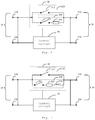
Fig. 1 is a schematic structural view of the charging device provided by embodiments of the present disclosure; -
Fig. 2 is a schematic structural view of the charging device provided by embodiments of the present disclosure; -
Fig. 3 is a schematic structural view of the charging device provided by embodiments of the present disclosure; -
Fig. 4 is a schematic structural view of the charging device provided by embodiments of the present disclosure; -
Fig. 5 is a schematic structural view of the charging device provided by embodiments of the present disclosure; -
Fig. 6 is a schematic structural view of the charging device provided by embodiments of the present disclosure; -
Fig. 7 is a schematic structural view of the charging device provided by embodiments of the present disclosure; -
Fig. 8 is a schematic structural view of the charging device provided by embodiments of the present disclosure; -
Fig. 9 is a schematic structural view of the charging device provided by embodiments of the present disclosure; -
Fig. 10 is a schematic structural view of the charging device provided by embodiments of the present disclosure. -
- 10 DC bus access terminal
- 110 DC bus positive access terminal
- 120 DC bus negative access terminal
- 20 load access terminal
- 210 load positive access terminal
- 220 load negative access terminal
- 30 charging circuit
- 310 first switch circuit
- 311 first switch
- 320 second switch circuit
- 321 second switch
- 322 current-limiting unit
- 323 current-limiting resistor
- 324 current-limiting inductor
- 330 relay
- 331 first contact
- 332 second contact
- 40 control circuit
- 410 chip processor
- 420 first sampling unit
- 421 first operational amplifier
- 430 second sampling unit
- 431 second operational amplifier
- 440 current sensor
- 450 power meter
- 460 battery display screen
- In order to make the object, technical solution and advantages of the present disclosure more explicitly understood, the charging device in the present disclosure will be described in further detail below in conjunction with the accompanying drawings and embodiments. It should be understood that, the specific embodiments described here are only intended to explain the present disclosure, rather than limiting the present disclosure.
- The present disclosure provides a charging device. It should be noted that, the charging device provided in the present disclosure is not only limited to disclosure in a single charging scenario. In any charging scenario, the charging device provided in the present disclosure may be used. In some embodiments, the charging device provided in the present disclosure is prepared for disclosure in a Micro DC-grid system to pre-charge a capacitive load.
- As shown in
Fig. 1 , in embodiments of the present disclosure, the charging device comprises a DCbus access terminal 10, aload access terminal 20, a chargingcircuit 30 and acontrol circuit 40. In embodiments of the present disclosure, the load is a capacitive load. For example, the load may be a capacitor. In the present disclosure, the chargingcircuit 30 is independently separated from the load to form the charging device with thecontrol circuit 40, the DCbus access terminal 10 and theload access terminal 20, so that there is no need to add a chargingcircuit 30 for the capacitive load itself. When the capacitive load needs to be charged, it suffices by supplementing the charging device in use. The charging device not only greatly reduces the production cost of the capacitive load, but also makes the charging process of the capacitive load more convenient. - In some embodiments, the DC
bus access terminal 10 shown is configured for electrical connection with the DC bus, so that the charging device is electrically connected to the DC bus. For example, the DCbus access terminal 10 may comprise at least one DC bus access contact. The DC bus access contact is configured for electrical connection with the DC bus. - In some embodiments, the
load access terminal 20 is configured for electrical connection with the load to be charged, so that the charging device is electrically connected to the load to be charged. For example, theload access terminal 20 may comprise at least one load access contact. The load access contact is configured for electrical connection with the load. - In some embodiments, the input terminal of the charging
circuit 30 is electrically connected to the DCbus access terminal 10. The output terminal of the chargingcircuit 30 is electrically connected to theload access terminal 20. The chargingcircuit 30 allows that electric energy of the DC bus can be charged into the load to be charged. In other words, the chargingcircuit 30 may act as a "bridge" between the DC bus and the load. - In some embodiments, the
control circuit 40 is electrically connected to the chargingcircuit 30. Thecontrol circuit 40 is configured to control the chargingcircuit 30 to complete charging. For example, thecontrol circuit 40 may deliver an instruction to the chargingcircuit 30 to allow the chargingcircuit 30 to start/interrupt charging. - As shown in
Fig. 2 , in embodiments of the present disclosure, the DCbus access terminal 10 comprises a DC buspositive access terminal 110 and a DC busnegative access terminal 120. Thepositive access terminal 110 of the DC bus is electrically connected to the anode of the DC bus. Thenegative access terminal 120 of the DC bus is electrically connected to the cathode of the DC bus. - In some embodiments, the DC bus may comprise an anode and a cathode. The DC bus
positive access terminal 110 and the DC busnegative access terminal 120 may be two contacts projecting from the charging device. - In embodiments of the present disclosure, the
load access terminal 20 comprises a loadpositive access terminal 210 and a loadnegative access terminal 220. The loadpositive access terminal 210 is electrically connected to the anode of the load to be charged. The loadnegative access terminal 220 is electrically connected to the cathode of the load to be charged. - In some embodiments, the load to be charged may comprise an anode and a cathode. The load
positive access terminal 210 and the loadnegative access terminal 220 may be two contacts projecting from the charging device. - In some embodiments, the load to be charged may be a capacitive load. For example, the load to be charged may be a capacitor.
- As shown in
Fig. 3 , in embodiments of the present disclosure, the chargingcircuit 30 comprises afirst switch circuit 310 and asecond switch circuit 320. Thefirst switch circuit 310 and thesecond switch circuit 320 are connected in parallel. - In some embodiments, the
first switch circuit 310 comprises afirst switch 311. One end of thefirst switch 311 is electrically connected to the DC buspositive access terminal 110. The other end of thefirst switch 311 is electrically connected to the loadpositive access terminal 210. - In some embodiments, the
second switch circuit 320 comprises asecond switch 321 and a current-limitingunit 322 connected in series with thesecond switch 321. One end of thesecond switch 321 is electrically connected to the DC buspositive access terminal 110, and the other end of thesecond switch 321 is electrically connected to one end of the current-limitingunit 322. The other end of the current-limitingunit 322 is electrically connected to the load to be charged. - In some embodiments, the function of the current-limiting
unit 322 is to produce a current-limiting effect when the charging device charges the load to be charged. When the load to be charged is thermally accessed into the Micro DC-grid system to charge the load to be charged, if there is an excessive voltage difference between the DC bus voltage and a rated voltage of the load to be charged, it is possible to cause an excessive charging current, so that the load to be charged may be damaged due to breakdown by the charging current. - As shown in
Fig. 6 , in embodiments of the present disclosure, the current-limitingunit 322 comprises at least one current-limitingresistor 323. The plurality of current-limitingresistors 323 are connected in series with each other. - As shown in
Fig. 7 , in embodiments of the present disclosure, the current-limitingunit 322 further comprises at least one current-limitinginductor 324, which is connected in series with the at least one current-limitingresistor 323. - The current-limiting
unit 322 in the present disclosure is not limited to which electronic element or in which connection manner an electronic element is connected, and it suffices as long as the current-limitingunit 322 can realize the current-limiting function. - In the Micro DC-grid system, the voltage of the DC bus has multiple voltage levels such as 750V, 400V and 200V. The voltage level of the DC bus may vary according to different Micro DC-grid systems. In the traditional solution, the load to be charged has its
own charging circuit 30, so that the load to be charged can only be adapted to a unique DC bus voltage. Once the DC bus of a high-voltage level is accessed, the load to be charged may be damaged due to an excessive charging current. - In embodiments of the present disclosure, the total resistance value of the current-limiting
unit 322 is set to be adjustable. The current-limitingunit 322 may automatically adjust the total resistance value of the current-limitingunit 322 according to a voltage of the DC bus, so that the charging current is adapted to the load to be charged. - In embodiments of the present disclosure, the total resistance value of the current-limiting
unit 322 is a preset value. The preset value is set to match the highest voltage level of the DC bus. It may be understood that, after the total resistance value of the current-limitingunit 322 is set to match the highest voltage level of the DC bus, the charging current is sufficiently small so that it is possible to be adapted to all DC buses of different voltage levels. - In the above-described embodiments of the present disclosure, the charging
circuit 30 is independently separated to make a charging device, and a current-limitingunit 322 is provided in the chargingcircuit 30. During charging, the charging device may be automatically adapted to DC buses of different voltage levels through the current-limitingunit 322, so that the charging device meets the needs of different voltage levels of the DC bus and different said loads to be charged, with favorable versatility and convenient charging. - As shown in
Fig. 4 , in embodiments of the present disclosure, thecontrol circuit 40 comprises achip processor 410. Thechip processor 410 is electrically connected to the chargingcircuit 30, for controlling thefirst switch 311 and thesecond switch 321 to be on or off, so as to control the chargingcircuit 30 to complete a charging process. - For example, after the charging device is connected to the DC bus and the load to be charged, the
chip processor 410 sends a first instruction to the chargingcircuit 30 so that thefirst switch 311 is off, and thesecond switch 321 is on, and the chargingcircuit 30 starts charging. At this time, the current-limitingunit 322 connected in series with thesecond switch 321 is accessed into the chargingcircuit 30 to produce a current-limiting effect, limit the magnitude of the charging current, and ensure the safety of the charging process. - After the power of the load to be charged reaches the requirement, the
chip processor 410 sends a second instruction to the chargingcircuit 30, so that thefirst switch 311 is on, thesecond switch 321 is off, and the chargingcircuit 30 ends charging. At this time, the current-limitingunit 322 connected in series with thesecond switch 321 loses its function, and the charging is completed. - As shown in
Fig. 5 , in embodiments of the present disclosure, the chargingcircuit 30 comprises arelay 330. Thefirst switch 311 is thefirst contact 331 of therelay 330. Thesecond switch 321 is thesecond contact 332 of therelay 330. The current-limitingunit 322 is connected in series with thesecond contact 332. - In some embodiments, the charging
circuit 30 is implemented by therelay 330 and the current-limitingunit 322. Thefirst switch 311 is thefirst contact 331 of therelay 330. Thesecond switch 321 is thesecond contact 332 of therelay 330. - For example, after the charging device is connected to the DC bus and the load to be charged, the
chip processor 410 sends a third instruction to therelay 330, so that thefirst contact 331 is off, and thesecond contact 332 is on, and the chargingcircuit 30 starts charging. At this time, the current-limitingunit 322 connected in series with thesecond contact 332 is connected to the chargingcircuit 30 to produce a current-limiting effect, limit the magnitude of the charging current, and ensure the safety of the charging process. - After the
chip processor 410 determines that the charging of the load to be charged is completed, thechip processor 410 sends a fourth instruction to therelay 330, so that thefirst contact 331 is on, and thesecond contact 332 is off, and the chargingcircuit 30 ends charging. At this time, the current-limitingunit 322 connected in series with thesecond contact 332 loses its function, and the charging is completed. - The following content introduces how the
chip processor 410 determines whether the charging of the load to be charged is completed. - As shown in
Fig. 8 , in embodiments of the present disclosure, thecontrol circuit 40 further comprises afirst sampling unit 420 and asecond sampling unit 430. - One end of the
first sampling unit 420 is electrically connected to the DC buspositive access terminal 110. The other end of thefirst sampling unit 420 is electrically connected to thechip processor 410. Thefirst sampling unit 420 is configured to collect a first voltage when the chargingcircuit 30 charges the load to be charged. The first voltage is a voltage across the DC bus. - One end of the
second sampling unit 430 is electrically connected to the loadpositive access terminal 210. The other end of thesecond sampling unit 430 is electrically connected to thechip processor 410. Thesecond sampling unit 430 is configured to collect a second voltage when the chargingcircuit 30 charges the load to be charged. The second voltage is a voltage across the load. - The
chip processor 410 determines whether the load to be charged is completed according to the difference between the first voltage and the second voltage. If the difference between the first voltage and the second voltage is less than a preset threshold, thechip processor 410 determines that the charging of the load to be charged is completed. - In some embodiments, the
first sampling unit 420 and thesecond sampling unit 430 are configured to collect the voltage across the DC bus and the voltage across the load to be charged respectively, that is, the first voltage and the second voltage, so as to determine whether the charging process is completed. - In embodiments of the present disclosure, the preset threshold is 1% of the first voltage.
- In embodiments of the present disclosure, the
chip processor 410 presets a charging time. If the difference between the first voltage and the second voltage is less than a preset threshold within the charging time, thechip processor 410 makes an alarm. The alarm may be implemented in multiple ways, such that it may be implemented by an alarm lamp or may be implemented by an alarm sound. In embodiments of the present disclosure, thechip processor 410 is electrically connected to an upper computer. In embodiments of the present disclosure, after an elapse of delay for a preset time, thechip processor 410 sends an alarm signal to the upper computer, so as to inform the upper computer that there is a fault in the chargingcircuit 30. - As shown in
Fig. 9 , in embodiments of the present disclosure, thefirst sampling unit 420 comprises a firstoperational amplifier 421, a resistor R1, a resistor R2, a resistor R3, a resistor R4 and a resistor R5. - One end of the resistor R1 is electrically connected to the DC bus
positive access terminal 110. The other end of the resistor R1 is electrically connected to the non-inverting input terminal of the firstoperational amplifier 421. - One end of the resistor R2 is electrically connected to the
negative access terminal 120 of the DC bus. The other end of the resistor R2 is electrically connected to the inverting input terminal of the firstoperational amplifier 421. The other end of the resistor R2 is also electrically connected to one end of the resistor R4. - One end of the resistor R4 is also electrically connected to the inverting input terminal of the first
operational amplifier 421. The other end of the resistor R4 is electrically connected to the output terminal of the firstoperational amplifier 421. - One end of the resistor R3 is grounded, and the other end of the resistor R3 is electrically connected to the non-inverting input terminal of the first
operational amplifier 421. - The output terminal of the first
operational amplifier 421 is electrically connected to thechip processor 410. - In some embodiments, the
second sampling unit 430 comprises a secondoperational amplifier 431, a resistor R5, a resistor R6, a resistor R7, and a resistor R8. - One end of the resistor R5 is electrically connected to the load
positive access terminal 210. The other end of the resistor R5 is electrically connected to the non-inverting input terminal of the secondoperational amplifier 431. - One end of the resistor R6 is electrically connected to the load
negative access terminal 220. The other end of the resistor R6 is electrically connected to the inverting input terminal of the secondoperational amplifier 431. The other end of the resistor R6 is also electrically connected to one end of the resistor R8. - One end of the resistor R8 is also electrically connected to the inverting input terminal of the second
operational amplifier 431. The other end of the resistor R8 is electrically connected to the output terminal of the secondoperational amplifier 431. - One end of the resistor R7 is grounded. The other end of the resistor R7 is electrically connected to the non-inverting input terminal of the second
operational amplifier 431. - The output terminal of the second
operational amplifier 431 is electrically connected to thechip processor 410. - As shown in
Fig. 10 , in embodiments of the present disclosure, thecontrol circuit 40 further comprises acurrent sensor 440 and apower meter 450. - One end of the
current sensor 440 is electrically connected to the DCbus access terminal 10. The other end of thecurrent sensor 440 is electrically connected to thechip processor 410. Thecurrent sensor 440 is configured to collect the current signal input from the DC bus to the charging device. - One end of the
power meter 450 is electrically connected to thecurrent sensor 440. The other end of thepower meter 450 is electrically connected to thechip processor 410. Thepower meter 450 is configured to calculate the power charged into the load to be charged according to the current signal and the voltage signal input to the charging device from the DC bus. Thepower meter 450 is also configured to send the power charged into the load to be charged to thechip processor 410. - In some embodiments, the
current sensor 440 and thepower meter 450 are provided in thecontrol circuit 40, to realize the metering function of the power to be charged into the load, so that the user may visually observe the household power, in a convenient and fast manner. - In embodiments of the present disclosure, the charging device further comprises a power display screen 460. The power display screen 460 is electrically connected to the
chip processor 410 and configured to display the power charged into the load to be charged. - In the above-described charging device, the charging
circuit 30 is independently provided as a charging device. First of all, the chargingcircuit 30 is controlled by thecontrol circuit 40 to charge electric energy of the DC bus into the load to be charged, so that it is possible to be compatible with a plurality of voltage levels of the DC bus and implement that the capacitive DC load is thermally accessed into the Micro DC-grid system in a safe and reliable manner. Next, the current-limitingunit 322 is provided so that the charging device may serve as a universal charging device, which is compatible with a plurality of voltage levels of said DC bus and the load to be charged. Finally, the charging device may also realize the power metering function through thecurrent sensor 440 and thepower meter 450, in a convenient and practical manner. - The present disclosure also provides a charging system, which is applied to a Micro DC-grid system, wherein the charging system comprises the charging device mentioned in the foregoing content.
- Various technical features of the above-described embodiments may be combined arbitrarily. In order to make a concise illustration, all possible combinations of various technical features in the above-described embodiments are not described. However, as long as there is no contradiction in the combinations of these technical features, they should be considered as the scope recited in this specification.
- The above-described embodiments only express several implementations of the present disclosure, in relatively specific and detailed descriptions, but cannot thus be understood as limiting the scope of the patent disclosure. It should be set forth that, for those of ordinary skill in the art, without departing from the concept of the present disclosure, several modifications and improvements may also be made, and all these fall within the protection scope of the present disclosure. Therefore, the protection scope of the present patent disclosure shall be subject to the appended claims.
Claims (13)
- A charging device, characterized in that the charging device comprises:a Direct Current (DC) bus access terminal (10) configured for electrical connection with a DC bus, to electrically connect the charging device to the DC bus;a load access terminal (20) configured for electrical connection with a load to be charged, to electrically connect the charging device to the load to be charged;a charging circuit (30) having an input terminal electrically connected to the DC bus access terminal (10), and an output terminal electrically connected to the load access terminal (20), to charge electrical energy of the DC bus into the load to be charged; anda control circuit (40) electrically connected to the charging circuit (30), for controlling the charging circuit (30) to complete a charging process.
- The charging device according to claim 1, characterized in that wherein:
the DC bus access terminal (10) comprises:a DC bus positive access terminal (110) electrically connected to an anode of the DC bus, anda DC bus negative access terminal (120) electrically connected to a cathode of the DC bus; andthe load access terminal (20) comprises:a load positive input terminal (210) electrically connected to an anode of the load to be charged, anda load negative access terminal (220) electrically connected to a cathode of the load to be charged. - The charging device according to claim 2, characterized in that the charging circuit (30) comprises:a first switch circuit (310) comprising a first switch (311), wherein one end of the first switch (311) is electrically connected to the DC bus positive access terminal (110), and the other end of the first switch (311) is electrically connected to the load positive access terminal (210); anda second switch circuit (320) comprising a second switch (321) and a current-limiting unit (322) connected in series with the second switch (321), wherein one end of the second switch (321) is electrically connected to the DC bus positive access terminal (110), and the other end of the second switch (321) is electrically connected to one end of the current-limiting unit (322), and the other end of the current-limiting unit (322) is electrically connected to the load to be charged, and the first switch circuit (310) is connected in parallel with the second switch circuit (320).
- The charging device according to claim 3, characterized in that wherein:the charging circuit (30) comprises a relay (330);the first switch (311) is a first contact (331) of the relay;the second switch (321) is a second contact (332) of the relay; andthe current-limiting unit (322) is connected in series with the second contact (332).
- The charging device according to claim 3, characterized in that the control circuit (40) comprises:
a chip processor (410) electrically connected to the charging circuit (30), for controlling the first switch (311) and the second switch (321) to be on or off, so as to control the charging circuit (30) to complete a charging process. - The charging device according to claim 3, characterized in that the current-limiting unit (322) comprises:
at least one current-limiting resistor (323), wherein the plurality of current-limiting resistors (323) are connected in series with each other. - The charging device according to claim 6, characterized in that the current-limiting unit (322) further comprises:
at least one current-limiting inductor (324), connected in series with the current-limiting resistor (323). - The charging device according to claim 5, characterized in that the control circuit (40) further comprises:a first sampling unit (420), of which one end is electrically connected to the DC bus positive access terminal (110), and the other end is electrically connected to the chip processor (410), the first sampling unit (420) is configured for collecting a first voltage across the DC bus when the charging circuit (30) charges the load to be charged, anda second sampling unit (430), wherein one end of the second sampling unit (430) is electrically connected to the load positive access terminal (210), and the other end is electrically connected to the chip processor (410), for collecting a second voltage when the charging circuit (30) charges the load to be charged, wherein the second voltage is a voltage across the load, andwherein the chip processor (410) is configured to determine whether charging of the load to be charged is completed according to a difference between the first voltage and the second voltage, and determine the charging of the load to be charged is completed if the difference between the first voltage and the second voltage is less than a preset threshold.
- The charging device according to claim 8, characterized in that, wherein:
the first sampling unit (420) comprises:a first operational amplifier (421), a resistor (R1), a resistor (R2), a resistor (R3), a resistor (R4) and a resistor (R5);one end of the resistor (R1) is electrically connected to the DC bus positive access terminal (110), and the other end of the resistor (R1) is electrically connected to a non-inverting input terminal of the first operational amplifier (421);one end of the resistor (R2) is electrically connected to the DC bus negative input terminal (120), the other end of the resistor (R2) is electrically connected to an inverting input terminal of the first operational amplifier (421), and the other end of the resistor (R2) is also electrically connected to one end of the resistor (R4);one end of the resistor (R4) is electrically connected to the inverting input terminal of the first operational amplifier (421), and the other end of the resistor (R4) is electrically connected to an output terminal of the first operational amplifier (421);one end of the resistor (R3) is grounded, and the other end of the resistor (R3) is electrically connected to the non-inverting input terminal of the first operational amplifier (421); andthe output terminal of the first operational amplifier (421) is electrically connected to the chip processor (410). - The charging device according to claim 8, characterized in that, wherein:the second sampling unit (430) comprises a second operational amplifier (431), a resistor (R5), a resistor (R6), a resistor (R7) and a resistor (R8);one end of the resistor (R5) is electrically connected to the load positive input terminal (210), and the other end of the resistor (R5) is electrically connected to a non-inverting input terminal of the second operational amplifier (431);one end of the resistor (R6) is electrically connected to the load negative input terminal (220), the other end of the resistor (R6) is electrically connected to an inverting input terminal of the second operational amplifier (431), and the other end of the resistor (R6) is also electrically connected to one end of the resistor (R8);one end of the resistor (R8) is electrically connected to the inverting input terminal of the second operational amplifier (431), and the other end of the resistor (R8) is electrically connected to an output terminal of the second operational amplifier (431);one end of the resistor (R7) is grounded, and the other end of the resistor (R7) is electrically connected to the non-inverting input terminal of the second operational amplifier (431); andthe output terminal of the second operational amplifier (431) is electrically connected to the chip processor (410).
- The charging device according to claim 5, characterized in that the control circuit (40) further comprises:a current sensor (440) having one end electrically connected to the DC bus access terminal (10), and the other end electrically connected to the chip processor (410), for collecting a current signal input from the DC bus to the charging device ; anda power meter (450) having one end electrically connected to the current sensor (440), and another end electrically connected to the chip processor (410), for calculating power charged into the load to be charged according to a current signal and a voltage signal input to the charging device by the DC bus, and sending the power charged into the load to be charged to the chip processor (410).
- The charging device of claim 11, characterized in that the charging device further comprises:
a power display screen (460), electrically connected to the chip processor (410), for displaying the power charged into the load to be charged. - A charging system applied to a Micro DC-grid system, characterized in that the charging system comprises the charging device according to any one of claims 1-12.
Applications Claiming Priority (2)
| Application Number | Priority Date | Filing Date | Title |
|---|---|---|---|
| CN201811073097.3A CN109038762B (en) | 2018-09-14 | 2018-09-14 | Charging device and charging system |
| PCT/CN2018/121911 WO2020052142A1 (en) | 2018-09-14 | 2018-12-19 | Charging device and charging system |
Publications (2)
| Publication Number | Publication Date |
|---|---|
| EP3826129A1 true EP3826129A1 (en) | 2021-05-26 |
| EP3826129A4 EP3826129A4 (en) | 2021-10-06 |
Family
ID=64621804
Family Applications (1)
| Application Number | Title | Priority Date | Filing Date |
|---|---|---|---|
| EP18933206.7A Pending EP3826129A4 (en) | 2018-09-14 | 2018-12-19 | CHARGING DEVICE AND CHARGING SYSTEM |
Country Status (6)
| Country | Link |
|---|---|
| US (1) | US20210249884A1 (en) |
| EP (1) | EP3826129A4 (en) |
| JP (1) | JP2022511279A (en) |
| KR (1) | KR20210057725A (en) |
| CN (1) | CN109038762B (en) |
| WO (1) | WO2020052142A1 (en) |
Families Citing this family (3)
| Publication number | Priority date | Publication date | Assignee | Title |
|---|---|---|---|---|
| CN109038762B (en) * | 2018-09-14 | 2020-07-14 | 珠海格力电器股份有限公司 | Charging device and charging system |
| EP3955412A4 (en) * | 2019-05-08 | 2022-06-15 | Guangdong Oppo Mobile Telecommunications Corp., Ltd. | LOADING AND DISCHARGE MEANS AND METHOD AND TERMINAL DEVICE |
| CN117644784B (en) * | 2023-11-30 | 2024-08-06 | 东莞市港奇电子有限公司 | Single-phase alternating-current charging overcurrent protection circuit and charger using same |
Family Cites Families (27)
| Publication number | Priority date | Publication date | Assignee | Title |
|---|---|---|---|---|
| JPH04101622A (en) * | 1990-08-17 | 1992-04-03 | Nec Ibaraki Ltd | Inserting and removing circuit for hot-line |
| JP3260053B2 (en) * | 1995-01-27 | 2002-02-25 | 株式会社ケンウッド | Battery voltage detection circuit for electrical equipment |
| JP2002350476A (en) * | 2001-05-23 | 2002-12-04 | Nagano Japan Radio Co | Voltage detection circuit |
| US6664758B2 (en) * | 2002-03-29 | 2003-12-16 | Fu-I Yang | Universal power adapter |
| AU2003279616A1 (en) * | 2002-06-28 | 2004-01-19 | Advanced Bionics Corporation | Microstimulator having self-contained power source and bi-directional telemetry system |
| DE10247112B3 (en) * | 2002-10-09 | 2004-08-26 | Siemens Ag | Method and device for switching on a circuit breaker arranged between capacitive elements |
| JP2007242247A (en) * | 2006-03-03 | 2007-09-20 | Fuji Heavy Ind Ltd | Control device for vehicle power supply system |
| US8618692B2 (en) * | 2007-12-04 | 2013-12-31 | Solaredge Technologies Ltd. | Distributed power system using direct current power sources |
| JP4649489B2 (en) * | 2008-03-27 | 2011-03-09 | 株式会社日立製作所 | Total battery voltage detection circuit |
| CN102487211B (en) * | 2010-12-03 | 2015-04-22 | 比亚迪股份有限公司 | Battery charging equipment |
| JP5255086B2 (en) * | 2011-04-08 | 2013-08-07 | 本田技研工業株式会社 | Power supply device and control method thereof |
| US8553373B2 (en) * | 2011-08-25 | 2013-10-08 | Hamilton Sundstrand Corporation | Solid state power controller for high voltage direct current systems |
| KR101542641B1 (en) * | 2011-09-23 | 2015-08-07 | 주식회사 엘지화학 | Battery charging system and method using the same |
| CN202679228U (en) * | 2012-07-26 | 2013-01-16 | 珠海格力电器股份有限公司 | Capacitor charging circuit |
| JP2014030108A (en) * | 2012-07-31 | 2014-02-13 | Sharp Corp | Power control device, storage battery and power control system |
| EP2898583B1 (en) * | 2012-09-18 | 2018-04-18 | Sonova AG | Method for charging a nimh battery, a battery charger and a system comprising a battery charger and a hearing device |
| CN104038042B (en) * | 2013-03-04 | 2016-12-28 | 珠海格力电器股份有限公司 | interleaved power factor correction circuit and control method thereof |
| JP6048363B2 (en) * | 2013-10-16 | 2016-12-21 | 株式会社デンソー | Current limiting relay device and power supply device |
| CN103762582B (en) * | 2014-01-20 | 2016-04-13 | 华中科技大学 | A kind of three-dimensional DC-DC converter |
| JP6643566B2 (en) * | 2015-05-28 | 2020-02-12 | パナソニックIpマネジメント株式会社 | Backup power supply and vehicle equipped with it |
| WO2017030321A1 (en) * | 2015-08-20 | 2017-02-23 | 주식회사 아이티엠반도체 | Battery protection circuit module and battery pack comprising same |
| US20180254644A1 (en) * | 2017-03-06 | 2018-09-06 | Intel Corporation | Techniques for charger control |
| GB201710818D0 (en) * | 2017-07-05 | 2017-08-16 | Oxis Energy Ltd | Battery Management |
| WO2019016991A1 (en) * | 2017-07-21 | 2019-01-24 | 三菱電機株式会社 | Power conversion device and power conversion system |
| WO2019077958A1 (en) * | 2017-10-17 | 2019-04-25 | 株式会社村田製作所 | Power supply device, power control device, and method for determining relay of power supply device |
| CN109038762B (en) * | 2018-09-14 | 2020-07-14 | 珠海格力电器股份有限公司 | Charging device and charging system |
| CN208707355U (en) * | 2018-09-14 | 2019-04-05 | 珠海格力电器股份有限公司 | charging device and charging system |
-
2018
- 2018-09-14 CN CN201811073097.3A patent/CN109038762B/en active Active
- 2018-12-19 JP JP2021510466A patent/JP2022511279A/en active Pending
- 2018-12-19 US US17/269,340 patent/US20210249884A1/en not_active Abandoned
- 2018-12-19 EP EP18933206.7A patent/EP3826129A4/en active Pending
- 2018-12-19 KR KR1020217006156A patent/KR20210057725A/en not_active Ceased
- 2018-12-19 WO PCT/CN2018/121911 patent/WO2020052142A1/en not_active Ceased
Also Published As
| Publication number | Publication date |
|---|---|
| EP3826129A4 (en) | 2021-10-06 |
| CN109038762B (en) | 2020-07-14 |
| JP2022511279A (en) | 2022-01-31 |
| CN109038762A (en) | 2018-12-18 |
| WO2020052142A1 (en) | 2020-03-19 |
| KR20210057725A (en) | 2021-05-21 |
| US20210249884A1 (en) | 2021-08-12 |
Similar Documents
| Publication | Publication Date | Title |
|---|---|---|
| US20170170653A1 (en) | Explosion-proof circuit, charging circuit and charging/discharging protection circuit of battery | |
| EP2887080A1 (en) | Power supply apparatus | |
| CN107370201A (en) | DC power system based on battery connection in series-parallel combination | |
| CN108248419A (en) | Energy storage battery charging and discharging system and method and related equipment | |
| WO2020052393A1 (en) | Charging apparatus and charging system | |
| CN101667747A (en) | Conversion module for extracting working power from high-voltage power | |
| CN203984066U (en) | Intelligent charger circuit | |
| CN204578205U (en) | Possesses repeatedly the high frequency combined switch electric power of lower electricity and accumulator protecting function | |
| US20210249884A1 (en) | Charging Device and Charging System | |
| CN109283445B (en) | Insulation detection method and controller of energy storage type rail vehicle charging system | |
| CN202374006U (en) | Lithium ion battery charging power supply with activation function | |
| CN104682543A (en) | Hybrid power supply system based on direct-current frequency variable power generator set | |
| CN207964998U (en) | A kind of test device of li-ion cell protection system | |
| CN2884649Y (en) | High voltage large capacity pulse current capacitor constant current charger | |
| CN211376863U (en) | a battery pack | |
| CN105529782B (en) | Online storage battery pack lagging battery emergency auxiliary system and working method thereof | |
| CN206593781U (en) | Being taken for 10kV switch ring main unit electric field inductions can temperature measuring equipment | |
| CN205123287U (en) | Generating set parallel machine synchro control device | |
| CN109831023A (en) | Middle straightening stream power distribution network black starting-up secondary device power supply unit | |
| CN203352148U (en) | Lithium battery protection system | |
| CN203502529U (en) | Switching on/of judging circuit of electric leakage reclosure breaker | |
| CN216751241U (en) | Prevent circuit and battery maintenance ware of striking sparks | |
| CN207234494U (en) | A kind of power outlet of Anti-surging | |
| CN221828614U (en) | A high voltage direct current power supply system | |
| CN203457098U (en) | Charging circuit for high-voltage variable-frequency speed control system |
Legal Events
| Date | Code | Title | Description |
|---|---|---|---|
| STAA | Information on the status of an ep patent application or granted ep patent |
Free format text: STATUS: THE INTERNATIONAL PUBLICATION HAS BEEN MADE |
|
| PUAI | Public reference made under article 153(3) epc to a published international application that has entered the european phase |
Free format text: ORIGINAL CODE: 0009012 |
|
| STAA | Information on the status of an ep patent application or granted ep patent |
Free format text: STATUS: REQUEST FOR EXAMINATION WAS MADE |
|
| 17P | Request for examination filed |
Effective date: 20210219 |
|
| AK | Designated contracting states |
Kind code of ref document: A1 Designated state(s): AL AT BE BG CH CY CZ DE DK EE ES FI FR GB GR HR HU IE IS IT LI LT LU LV MC MK MT NL NO PL PT RO RS SE SI SK SM TR |
|
| A4 | Supplementary search report drawn up and despatched |
Effective date: 20210902 |
|
| RIC1 | Information provided on ipc code assigned before grant |
Ipc: H02J 7/00 20060101AFI20210827BHEP |
|
| DAV | Request for validation of the european patent (deleted) | ||
| DAX | Request for extension of the european patent (deleted) | ||
| P01 | Opt-out of the competence of the unified patent court (upc) registered |
Effective date: 20230530 |
|
| REG | Reference to a national code |
Ref country code: DE Ref legal event code: R079 Free format text: PREVIOUS MAIN CLASS: H02J0007000000 Ipc: H02J0007620000 |
|
| GRAP | Despatch of communication of intention to grant a patent |
Free format text: ORIGINAL CODE: EPIDOSNIGR1 |
|
| STAA | Information on the status of an ep patent application or granted ep patent |
Free format text: STATUS: GRANT OF PATENT IS INTENDED |
|
| RIC1 | Information provided on ipc code assigned before grant |
Ipc: H02J 7/62 20260101AFI20260224BHEP Ipc: H02J 7/96 20260101ALI20260224BHEP |
|
| INTG | Intention to grant announced |
Effective date: 20260313 |