EP3826110A1 - Antenna and communication device - Google Patents
Antenna and communication device Download PDFInfo
- Publication number
- EP3826110A1 EP3826110A1 EP19859575.3A EP19859575A EP3826110A1 EP 3826110 A1 EP3826110 A1 EP 3826110A1 EP 19859575 A EP19859575 A EP 19859575A EP 3826110 A1 EP3826110 A1 EP 3826110A1
- Authority
- EP
- European Patent Office
- Prior art keywords
- ring
- conductive portion
- split
- antenna
- present disclosure
- Prior art date
- Legal status (The legal status is an assumption and is not a legal conclusion. Google has not performed a legal analysis and makes no representation as to the accuracy of the status listed.)
- Withdrawn
Links
Images








Classifications
-
- H—ELECTRICITY
- H01—ELECTRIC ELEMENTS
- H01Q—ANTENNAS, i.e. RADIO AERIALS
- H01Q7/00—Loop antennas with a substantially uniform current distribution around the loop and having a directional radiation pattern in a plane perpendicular to the plane of the loop
-
- H—ELECTRICITY
- H01—ELECTRIC ELEMENTS
- H01Q—ANTENNAS, i.e. RADIO AERIALS
- H01Q9/00—Electrically-short antennas having dimensions not more than twice the operating wavelength and consisting of conductive active radiating elements
- H01Q9/04—Resonant antennas
- H01Q9/0407—Substantially flat resonant element parallel to ground plane, e.g. patch antenna
- H01Q9/0464—Annular ring patch
-
- H—ELECTRICITY
- H01—ELECTRIC ELEMENTS
- H01Q—ANTENNAS, i.e. RADIO AERIALS
- H01Q1/00—Details of, or arrangements associated with, antennas
- H01Q1/44—Details of, or arrangements associated with, antennas using equipment having another main function to serve additionally as an antenna, e.g. means for giving an antenna an aesthetic aspect
- H01Q1/46—Electric supply lines or communication lines
-
- H—ELECTRICITY
- H01—ELECTRIC ELEMENTS
- H01Q—ANTENNAS, i.e. RADIO AERIALS
- H01Q5/00—Arrangements for simultaneous operation of antennas on two or more different wavebands, e.g. dual-band or multi-band arrangements
- H01Q5/30—Arrangements for providing operation on different wavebands
- H01Q5/307—Individual or coupled radiating elements, each element being fed in an unspecified way
- H01Q5/342—Individual or coupled radiating elements, each element being fed in an unspecified way for different propagation modes
- H01Q5/35—Individual or coupled radiating elements, each element being fed in an unspecified way for different propagation modes using two or more simultaneously fed points
-
- H—ELECTRICITY
- H01—ELECTRIC ELEMENTS
- H01Q—ANTENNAS, i.e. RADIO AERIALS
- H01Q5/00—Arrangements for simultaneous operation of antennas on two or more different wavebands, e.g. dual-band or multi-band arrangements
- H01Q5/30—Arrangements for providing operation on different wavebands
- H01Q5/307—Individual or coupled radiating elements, each element being fed in an unspecified way
- H01Q5/342—Individual or coupled radiating elements, each element being fed in an unspecified way for different propagation modes
- H01Q5/357—Individual or coupled radiating elements, each element being fed in an unspecified way for different propagation modes using a single feed point
- H01Q5/364—Creating multiple current paths
-
- H—ELECTRICITY
- H01—ELECTRIC ELEMENTS
- H01Q—ANTENNAS, i.e. RADIO AERIALS
- H01Q5/00—Arrangements for simultaneous operation of antennas on two or more different wavebands, e.g. dual-band or multi-band arrangements
- H01Q5/30—Arrangements for providing operation on different wavebands
- H01Q5/307—Individual or coupled radiating elements, each element being fed in an unspecified way
- H01Q5/342—Individual or coupled radiating elements, each element being fed in an unspecified way for different propagation modes
- H01Q5/357—Individual or coupled radiating elements, each element being fed in an unspecified way for different propagation modes using a single feed point
- H01Q5/364—Creating multiple current paths
- H01Q5/371—Branching current paths
Definitions
- This invention relates to an antenna and a communication device.
- An antenna using a split-ring resonator is known as a small antenna used for a wireless communication device.
- a wireless communication device comprising a split-ring resonator is disclosed in Patent Document 1.
- Patent Document 1 WO2013/027824
- the number of a resonant frequency of the split-ring resonator is one.
- the antenna of Document 1 has a problem "how the antenna resonates at a plurality of resonant frequencies or has a broadband frequency response, while the antenna has advantages (small size and low manufacturing cost) of its split-ring resonator".
- an antenna may comprise a split-ring conductive portion and a ring-inside conductive portion, wherein: the split-ring conductive portion may be positioned outside a region and may be positioned in an area which extends along an outline of the region except for a split; the ring-inside conductive portion may be positioned inside the region; the ring-inside conductive portion may be continuous with one of parts of the split-ring conductive portion, the split being put between the parts of the split-ring conductive portion; and at least a part of the ring-inside conductive portion may be bent so as to extend parallel to the split-ring conductive portion.
- a communication device may comprise the antenna according to an aspect of the present disclosure.
- various aspects of the present disclosure can provide an antenna, which, while having advantages (small size and low manufacturing cost) of its split-ring resonator, resonates at a plurality of resonant frequencies or has a broadband frequency response, and can provide a communication device comprising the antenna.
- an antenna may comprise a split-ring conductive portion 101 and an ring-inside conductive portion 102, wherein: the split-ring conductive portion 101 may be positioned outside a region 103 and may be positioned in an area which extends along an outline of the region 103 except for a split 104; the ring-inside conductive portion 102 may be positioned inside the region 103; the ring-inside conductive portion 102 may be continuous with one of parts of the split-ring conductive portion 101, the split 104 being put between the parts of the split-ring conductive portion 101; and at least a part of the ring-inside conductive portion 102 may be bent so as to extend parallel to the split-ring conductive portion 101.
- the region 103 may be surrounded by the split-ring conductive portion 101 and the split 104.
- the region 103 may have any shape; it may have a shape of a polygon including a square, a rectangle, etc., a circle, an oval, etc.
- the split-ring conductive portion 101 may be formed of a metal plate.
- the split-ring conductive portion 101 may have any shape; it may have a shape based on an approximately C-shape along a rectangular-ring, or a shape based on a shape extending along one of various rings, such as a circular ring, an oval ring, a track-shaped ring, etc.
- the parts of the split-ring conductive portion 101, which are positioned so that the split 104 is put therebetween may comprise an auxiliary conductive portion 1011.
- the auxiliary conductive portion 1011 may be provided at the same layer where the split-ring conductive portion 101 is provided, or may be provided at a different layer from the layer where the split-ring conductive portion 101 is provided.
- the split 104 may be filled with nothing, or may be filled with resin or the like.
- the split 104 may have any shape; it may have a shape such as a straight line, a curved line, a zigzag line or the like.
- the split 104 may have a meander shape.
- the wording of the meander shape includes concept which is specified by the wordings such as a zigzag shape, a comb tooth shape, and a shape based on an interdigital structure.
- a meander shape is formed of a combination of a straight line, a curved line, a zigzag line, etc.
- the ring-inside conductive portion 102 may be formed of a metal plate.
- the ring-inside conductive portion 102 may be provided at the same layer where the split-ring conductive portion 101 is provided.
- a part of the split-ring conductive portion 101 other than another part of the split-ring conductive portion 101, which extends parallel to the ring-inside conductive portion 102, may be provided at a layer different from a layer where the ring-inside conductive portion 102 is provided.
- the ring-inside conductive portion 102 and the split-ring conductive portion 101 may be formed by cutting out them from one conductive board by a laser, etc.
- an antenna according to an aspect of the present disclosure can be recognized to comprise two resonant circuits.
- a first resonant circuit can be recognized to be composed of a capacitance, which is introduced in the split 104 by feeding RF (Radio Frequency) signal to the antenna, and an inductance introduced in the split-ring conductive portion 101 by feeding RF (Radio Frequency) signals to the antenna.
- the first resonant circuit can be recognized to produce a first resonant frequency.
- a second resonant circuit can be recognized to be composed of a capacitance, an inductance, another capacitance and another inductance, wherein: the capacitance is introduced in the split 104 by feeding RF signals to the antenna; the inductance is introduced in the ring-inside conductive portion 102 by feeding RF signals to the antenna; the another capacitance is introduced, by feeding RF signals to the antenna, between the split-ring conductive portion 101 and the part of the ring-inside conductive portion 102 extending parallel to the split-ring conductive portion 101; and the another inductance is introduced, by feeding RF signals to the antenna, in the part of the split-ring conductive portion 101 other than the another part of the split-ring conductive portion 101 extending parallel to the ring-inside conductive portion 102.
- the second resonant circuit can be recognized to produce a second resonant frequency.
- the resonant frequency of the first resonant circuit and the resonant frequency of the second resonant circuit can be recognized to be different from each other. If the resonant frequency of the first resonant circuit and the resonant frequency of the second circuit are configured to be away from each other, the antenna can resonate at a plurality of resonant frequencies. If the resonant frequency of the first resonant circuit and the resonant frequency of the second circuit are configured to be close to each other, the antenna can have a broadband frequency response.
- the resonant frequency of the second resonant circuit is higher than the resonant frequency of the first resonant circuit, the resonant frequency of the first resonant circuit and the resonant frequency of the second circuit can be adjusted to be close to each other by reducing the resonant frequency of the second resonant circuit.
- the resonant frequency of the second resonant circuit can be reduced, for example, in any of the following manners: a length of the ring-inside conductive portion 102 is enlarged; a distance between the split-ring conductive portion 101 and the part of the ring-inside conductive portion 102 extending parallel to the split-ring conductive portion 101 is reduced; a chip capacitor is arranged between the split-ring conductive portion 101 and the part of the ring-inside conductive portion 102 extending parallel to the split-ring conductive portion 101; and a region between the split-ring conductive portion 101 and the part of the ring-inside conductive portion 102 extending parallel to the split-ring conductive portion 101 is formed in a meander shape.
- an aspect of the present disclosure can provide an antenna, which, while having advantages (small size and low manufacturing cost) of its split-ring resonator, resonates at a plurality of resonant frequencies or has a broadband frequency response.
- an antenna according to an aspect of the present disclosure might have a wider frequency range, where a return loss of the antenna is equal to or less than a threshold "a", in comparison with an assumption where an antenna have a single resonant frequency.
- the threshold "a" is, for example, - 10 dB
- the present invention is not limited thereto and the antenna should be sufficiently operational under a state where the return loss of the antenna is equal to or less than the threshold "a"
- An antenna according to an aspect of the present disclosure may be formed as, for example, a component which is configured to be mounted on a substrate 2 or the like.
- An antenna according to an aspect of the present disclosure may be, for example, directly formed on the substrate 2.
- An antenna according to an aspect of the present disclosure may, for example, protrude from the substrate 2.
- An antenna according to an aspect of the present disclosure may be, for example, arranged substantially perpendicular to the substrate 2.
- an antenna according to an aspect of the present disclosure may be, for example, configured so that a distance between the split-ring conductive portion 101 and the part of the ring-inside conductive portion 102 extending parallel to the split-ring conductive portion 101 is smaller than a distance between the split-ring conductive portion 101 and another part of the ring-inside conductive portion 102 other than the part of the ring-inside conductive portion 102 extending parallel to the split-ring conductive portion 101.
- An antenna according to an aspect of the present disclosure may be, for example, configured so that the split-ring conductive portion 101 and the part of the ring-inside conductive portion 102 extending parallel to the split-ring conductive portion 101 may be closely positioned to each other enough to have a capacitance which contributes to a resonance of the antenna.
- the second resonant circuit can be recognized to be formed by the another capacitance which is introduced, by feeding RF signals to the antenna, between the split-ring conductive portion 101 and the part of the ring-inside conductive portion 102 extending parallel to the split-ring conductive portion 101.
- an antenna according to an aspect of the present disclosure which is for example the antenna 1A or their modifications, may be, for example, configured so that electrical power is supplied to the ring-inside conductive portion 102 by using connection of a feed line 105 with the ring-inside conductive portion 102 or is wirelessly supplied to the ring-inside conductive portion 102.
- the feed line 105 may be, for example, connected with any part of the ring-inside conductive portion 102, and impedances of an RF circuit and an antenna according to an aspect of the present disclosure can be matched to each other by adjusting a junction of the ring-inside conductive portion 102 with the feed line 105.
- the feed line 105 may be configured so that the feed line 105 is provided at a layer different from the layer, where the ring-inside conductive portion 102 is provided, while the feed line 105 is connected with the ring-inside conductive portion 102 through a via 3.
- the feed line 105 may be provided at the same layer where the ring-inside conductive portion 102 is provided, the feed line 105 may extend in the region 103, and the feed line 105 may extend along the split-ring conductive portion 101 or along a clearance provided on the substrate.
- the feed line 105 may be formed of a wire such as a transmission line or the like, or may be formed of a metal plate.
- the ring-inside conductive portion 102 and the metal plate part of the feed line 105 may be formed by cutting out them from one conductive board by a laser, etc.
- Wireless electrical power supply to the ring-inside conductive portion 102 may be done by, for example, using an EM (Electro-magnetic) coupling portion 106 with which the feed line 105 is connected.
- the EM coupling portion 106 may be, for example, electromagnetically connected with any part of the ring-inside conductive portion 102, and impedances of an RF circuit and an antenna according to an aspect of the present disclosure can be matched to each other by adjusting a part of the ring-inside conductive portion 102 which is electromagnetically connected with the EM coupling portion 106.
- the EM coupling portion 106 may be provided at a layer different from the layer where the ring-inside conductive portion 102 is provided.
- the EM coupling portion 106 may be provided at the same layer where the ring-inside conductive portion 102 is provided, the feed line 105 connected with the EM coupling portion 106 may extend in the region 103, and the feed line 105 connected with the EM coupling portion 106 may extend along the split-ring conductive portion 101 or along the clearance provided on the substrate.
- the EM coupling portion 106 may be formed of a metal plate.
- the ring-inside conductive portion 102 and the EM coupling portion 106 may be formed by cutting out them from one conductive board by a laser, etc.
- the EM coupling portion 106 and the metal plate part of the feed line 105 may be formed by cutting out them from one conductive board by a laser, etc.
- an antenna according to an aspect of the present disclosure has an excellent antenna characteristics in comparison with an assumption where electrical power is supplied not to the ring-inside conductive portion 102 but to the split-ring conductive portion 101 by using connection of a feed line or is wirelessly supplied thereto.
- an antenna according to an aspect of the present disclosure which is for example the antenna 1B or their modifications, may be, for example, configured so that electrical power is supplied to the split-ring conductive portion 101 by using connection of a feed line 107 with the split-ring conductive portion 101 or is wirelessly supplied thereto.
- the feed line 107 may be, for example, connected with any part of the split-ring conductive portion 101, and impedances of an RF circuit and an antenna according to an aspect of the present disclosure can be matched to each other by adjusting a junction of the split-ring conductive portion 101 with the feed line 107.
- the feed line 107 may be configured so that the feed line 107 is provided at a layer different from the layer, where the split-ring conductive portion 101 is provided, while the feed line 107 is connected with the split-ring conductive portion 101 through the via 3.
- the feed line 107 may be provided at the same layer where the split-ring conductive portion 101 is provided, the feed line 107 may extend in the region 103, and the feed line 107 may extend along the split-ring conductive portion 101 or along the clearance provided on the substrate.
- the feed line 107 may be formed of a wire such as a transmission line or the like, or may be formed of a metal plate.
- the split-ring conductive portion 101 and the metal plate part of the feed line 107 may be formed by cutting out them from one conductive board by a laser, etc.
- Wireless electrical power supply to the split-ring conductive portion 101 may be done by, for example, using an EM(Electro-magnetic) coupling portion 108 with which the feed line 107 is connected.
- the EM coupling portion 108 may be, for example, electromagnetically connected with any part of the split-ring conductive portion 101, and impedances of an RF circuit and an antenna according to an aspect of the present disclosure can be matched to each other by adjusting a part of the split-ring conductive portion 101 which is electromagnetically connected with the EM coupling portion 108.
- the EM coupling portion 108 may be provided at a layer different from the layer where the split-ring conductive portion 101 is provided.
- the EM coupling portion 108 may be provided at the same layer where the split-ring conductive portion 101 is provided, the feed line 107 connected with the EM coupling portion 108 may extend in the region 103, and the feed line 107 may extend along the split-ring conductive portion 101 or along the clearance provided on the substrate.
- the EM coupling portion 108 may be formed of a metal plate.
- the split-ring conductive portion 101 and the EM coupling portion 108 may be formed by cutting out them from one conductive board by a laser, etc.
- the EM coupling portion 108 and the metal plate part of the feed line 107 may be formed by cutting out them from one conductive board by a laser, etc.
- an antenna according to an aspect of the present disclosure is, for example, configured so that electrical power is directly supplied also to the first resonant circuit.
- an antenna according to an aspect of the present disclosure allows for finer tuning.
- an antenna according to an aspect of the present disclosure which is for example the antennas 1A, 1B, 1C or their modifications, may be, for example, configured as follows: the region 103 may have a substantially rectangular shape; the split 104 may be positioned around a corner, or a vertex, of the region 103; and the ring-inside conductive portion 102 may be configured so that a part of the ring-inside conductive portion 102 between a distal end of the ring-inside conductive portion 102 and a first bent of the ring-inside conductive portion 102, which counts from a junction of the ring-inside conductive portion 102 with the split-ring conductive portion 101, is bent once so as to extend parallel to the split-ring conductive portion 101.
- a distance between the split-ring conductive portion 101 and a part of the ring-inside conductive portion 102 between the distal end and a second bent of the ring-inside conductive portion 102, which counts from the junction with the split-ring conductive portion 101 may be smaller than a distance between the split-ring conductive portion 101 and another part of the ring-inside conductive portion 102 between two of the bents.
- An antenna according to an aspect of the present disclosure as described above can provide, for example, good response, in particular, over a wide frequency range.
- an antenna according to an aspect of the present disclosure may further comprise, for example, a ring-inside conductive portion 109, wherein: the ring-inside conductive portion 102 may be positioned outside a region 110 and may be positioned in an area which extends along an outline of the region 110 except for a split 111; the ring-inside conductive portion 109 may be positioned inside the region 110; the ring-inside conductive portion 109 may be continuous with one of parts of the ring-inside conductive portion 102, the split 111 being put between the parts of the ring-inside conductive portion 102; and at least a part of the ring-inside conductive portion 109 may be bent so as to extend parallel to the ring-inside conductive portion 102.
- the region 110 may be surrounded by the ring-inside conductive portion 102 and the split 111.
- the region 110 may have any shape; it may have a polygonal shape such as a square, a rectangle or the like, or a shape such as a circle, an oval or the like.
- the split 111 may be filled with nothing, and may be filled with resin or the like.
- the split 111 may have any shape; it may have a shape such as a straight line, a curved line, a zigzag line or the like.
- the split 111 may have a meander shape.
- the ring-inside conductive portion 109 may be formed of a metal plate.
- the ring-inside conductive portion 109 may be provided at the same layer where the ring-inside conductive portion 102 is provided.
- a part of the ring-inside conductive portion 102 other than another part of the ring-inside conductive portion 102, which extends parallel to the ring-inside conductive portion 109, may be provided at a layer different from the layer where the ring-inside conductive portion 109 is provided.
- the ring-inside conductive portion 109 and the ring-inside conductive portion 102 may be formed by cutting out them from one conductive board by a laser, etc.
- electrical power may be supplied to the ring-inside conductive portion 109 by using connection of a feed line with the ring-inside conductive portion 109 or may be wirelessly supplied to the ring-inside conductive portion 109.
- an antenna according to an aspect of the present disclosure as describe above can be recognized to further comprise a third resonant circuit.
- the third resonant circuit can be recognized to be composed of a capacitance, an inductance, another capacitance and another inductance, wherein: the capacitance is introduced in the split 111 by feeding RF signals to the antenna; the inductance is introduced in the ring-inside conductive portion 109 by feeding RF signals to the antenna; the another capacitance is introduced, by feeding RF signals to the antenna, between the ring-inside conductive portion 102 and a part of the ring-inside conductive portion 109 extending parallel to the ring-inside conductive portion 102; and the another inductance is introduced, by feeding RF signals to the antenna, in the part of the ring-inside conductive portion 102 other than the another part of the ring-inside conductive portion 102 extending parallel to the ring-inside conductive portion 109.
- an aspect of the present disclosure can provide an antenna
- ring-inside conductive portions are analogously formed in the region 103, the region 110, a region 112, etc., and thereby an aspect of the present disclosure can provide an antenna, which, while having an advantage (small size and low manufacturing cost) of its split-ring resonator, resonates at a plurality of resonant frequencies or has a broadband frequency response.
- a communication device may, for example, comprise an antenna according to an aspect of the present disclosure, which is for example the antennas 1A, 1B, 1C, 1D, 1E or their modifications.
- An aspect of the present disclosure as described above can provide a communication device which has a reduced size and provides good performance.
- the present invention has been described above in connection with the above-mentioned embodiments which are exemplary examples of antennas. However, the present invention is not limited to the embodiments as described above. Within the scope of the present invention, the present invention can provide for various embodiments that can be understood by a person skilled in the art.
Landscapes
- Details Of Aerials (AREA)
Abstract
Description
- This invention relates to an antenna and a communication device.
- An antenna using a split-ring resonator is known as a small antenna used for a wireless communication device. For example, a wireless communication device comprising a split-ring resonator is disclosed in Patent Document 1.
- Patent Document 1:
WO2013/027824 - In the antenna of Patent Document 1, the number of a resonant frequency of the split-ring resonator is one. Thus, the antenna of Document 1 has a problem "how the antenna resonates at a plurality of resonant frequencies or has a broadband frequency response, while the antenna has advantages (small size and low manufacturing cost) of its split-ring resonator".
- For example, an antenna according to an aspect of the present disclosure may comprise a split-ring conductive portion and a ring-inside conductive portion, wherein: the split-ring conductive portion may be positioned outside a region and may be positioned in an area which extends along an outline of the region except for a split; the ring-inside conductive portion may be positioned inside the region; the ring-inside conductive portion may be continuous with one of parts of the split-ring conductive portion, the split being put between the parts of the split-ring conductive portion; and at least a part of the ring-inside conductive portion may be bent so as to extend parallel to the split-ring conductive portion.
- A communication device according to an aspect of the present disclosure may comprise the antenna according to an aspect of the present disclosure.
- For example, various aspects of the present disclosure can provide an antenna, which, while having advantages (small size and low manufacturing cost) of its split-ring resonator, resonates at a plurality of resonant frequencies or has a broadband frequency response, and can provide a communication device comprising the antenna.
-
-
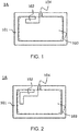
Fig. 1 is a view of an example of an antenna according to an aspect of the present disclosure. -
Fig. 2 is a view of an example of an antenna according to an aspect of the present disclosure. -
Fig. 3 is a view of an example of an antenna according to an aspect of the present disclosure. -
Fig. 4 is a view of an example of an antenna according to an aspect of the present disclosure. -
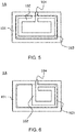
Fig. 5 is a view of an example of an antenna according to an aspect of the present disclosure. -
Fig. 6 is a view of an example of an antenna according to an aspect of the present disclosure. -
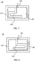
Fig. 7 is a view of an example of an antenna according to an aspect of the present disclosure. -
Fig. 8 is a view of an example of an antenna according to an aspect of the present disclosure. -
Fig. 9 is a view of an example of an antenna according to an aspect of the present disclosure. -
Fig. 10 is a view of an example of an antenna according to an aspect of the present disclosure. -
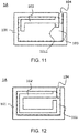
Fig. 11 is a view of an example of an antenna according to an aspect of the present disclosure. -
Fig. 12 is a view of an example of an antenna according to an aspect of the present disclosure. -
Fig. 13 is a view of an example of characteristics of an antenna according to an aspect of the present disclosure. -
Fig. 14 is a view of an example of an antenna according to an aspect of the present disclosure. -
Fig. 15 is a view of an example of an antenna according to an aspect of the present disclosure. -
Fig. 16 is a view of an example of an antenna according to an aspect of the present disclosure. -
Fig. 17 is a view of an example of an antenna according to an aspect of the present disclosure. -
Fig. 18 is a view of an example of an antenna according to an aspect of the present disclosure. -
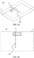
Fig. 19 is a view of an example of an antenna according to an aspect of the present disclosure. -
Fig. 20 is a view of an example of an antenna according to an aspect of the present disclosure. -
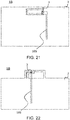
Fig. 21 is a view of an example of an antenna according to an aspect of the present disclosure. -
Fig. 22 is a view of an example of an antenna according to an aspect of the present disclosure. -
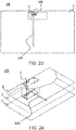
Fig. 23 is a view of an example of an antenna according to an aspect of the present disclosure. -
Fig. 24 is a view of an example of an antenna according to an aspect of the present disclosure. -
Fig. 25 is a view of an example of an antenna according to an aspect of the present disclosure. -
Fig. 26 is a view of an example of an antenna according to an aspect of the present disclosure. -
Fig. 27 is a view of an example of an antenna according to an aspect of the present disclosure. -
Fig. 28 is a view of an example of an antenna according to an aspect of the present disclosure. -
Fig. 29 is a view of an example of an antenna according to an aspect of the present disclosure. -
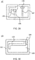
Fig. 30 is a view of an example of an antenna according to an aspect of the present disclosure. -
Fig. 31 is a view of an example of an antenna according to an aspect of the present disclosure. -
Fig. 32 is a view of an example of an antenna according to an aspect of the present disclosure. -
Fig. 33 is a view of an example of an antenna according to an aspect of the present disclosure. -
Fig. 34 is a view of an example of an antenna according to an aspect of the present disclosure. - All aspects according to the present disclosure are merely examples, and they are neither intended to exclude other examples from the present disclosure nor intended to limit technical features of the invention described in Claims.
- The description about combinations of the aspects according to the present disclosure may be partially omitted. Such omissions are intended to simplify the description, and they are neither intended to be excluded from the present disclosure nor intended to limit the technical scope of the invention described in Claims. All combinations of the aspects according to the present disclosure are included in the present disclosure either explicitly, implicitly or inherently with or without such omissions. Thus, all combinations of the aspects according to the present disclosure can be directly and clearly conceived from the present disclosure with or without such omission.
- As shown in
Figs. 1 to 12 , for example, an antenna according to an aspect of the present disclosure may comprise a split-ringconductive portion 101 and an ring-insideconductive portion 102, wherein: the split-ringconductive portion 101 may be positioned outside aregion 103 and may be positioned in an area which extends along an outline of theregion 103 except for asplit 104; the ring-insideconductive portion 102 may be positioned inside theregion 103; the ring-insideconductive portion 102 may be continuous with one of parts of the split-ringconductive portion 101, thesplit 104 being put between the parts of the split-ringconductive portion 101; and at least a part of the ring-insideconductive portion 102 may be bent so as to extend parallel to the split-ringconductive portion 101. - For example, the
region 103 may be surrounded by the split-ringconductive portion 101 and thesplit 104. For example, theregion 103 may have any shape; it may have a shape of a polygon including a square, a rectangle, etc., a circle, an oval, etc. - For example, the split-ring
conductive portion 101 may be formed of a metal plate. For example, the split-ringconductive portion 101 may have any shape; it may have a shape based on an approximately C-shape along a rectangular-ring, or a shape based on a shape extending along one of various rings, such as a circular ring, an oval ring, a track-shaped ring, etc. For example, the parts of the split-ringconductive portion 101, which are positioned so that thesplit 104 is put therebetween, may comprise an auxiliaryconductive portion 1011. The auxiliaryconductive portion 1011 may be provided at the same layer where the split-ringconductive portion 101 is provided, or may be provided at a different layer from the layer where the split-ringconductive portion 101 is provided. - For example, the
split 104 may be filled with nothing, or may be filled with resin or the like. For example, thesplit 104 may have any shape; it may have a shape such as a straight line, a curved line, a zigzag line or the like. For example, thesplit 104 may have a meander shape. The wording of the meander shape includes concept which is specified by the wordings such as a zigzag shape, a comb tooth shape, and a shape based on an interdigital structure. For example, a meander shape is formed of a combination of a straight line, a curved line, a zigzag line, etc. - For example, the ring-inside
conductive portion 102 may be formed of a metal plate. For example, the ring-insideconductive portion 102 may be provided at the same layer where the split-ringconductive portion 101 is provided. A part of the split-ringconductive portion 101 other than another part of the split-ringconductive portion 101, which extends parallel to the ring-insideconductive portion 102, may be provided at a layer different from a layer where the ring-insideconductive portion 102 is provided. For example, the ring-insideconductive portion 102 and the split-ringconductive portion 101 may be formed by cutting out them from one conductive board by a laser, etc. - For example, an antenna according to an aspect of the present disclosure can be recognized to comprise two resonant circuits. A first resonant circuit can be recognized to be composed of a capacitance, which is introduced in the
split 104 by feeding RF (Radio Frequency) signal to the antenna, and an inductance introduced in the split-ringconductive portion 101 by feeding RF (Radio Frequency) signals to the antenna. The first resonant circuit can be recognized to produce a first resonant frequency. A second resonant circuit can be recognized to be composed of a capacitance, an inductance, another capacitance and another inductance, wherein: the capacitance is introduced in thesplit 104 by feeding RF signals to the antenna; the inductance is introduced in the ring-insideconductive portion 102 by feeding RF signals to the antenna; the another capacitance is introduced, by feeding RF signals to the antenna, between the split-ringconductive portion 101 and the part of the ring-insideconductive portion 102 extending parallel to the split-ringconductive portion 101; and the another inductance is introduced, by feeding RF signals to the antenna, in the part of the split-ringconductive portion 101 other than the another part of the split-ringconductive portion 101 extending parallel to the ring-insideconductive portion 102. The second resonant circuit can be recognized to produce a second resonant frequency. As understood from above, the resonant frequency of the first resonant circuit and the resonant frequency of the second resonant circuit can be recognized to be different from each other. If the resonant frequency of the first resonant circuit and the resonant frequency of the second circuit are configured to be away from each other, the antenna can resonate at a plurality of resonant frequencies. If the resonant frequency of the first resonant circuit and the resonant frequency of the second circuit are configured to be close to each other, the antenna can have a broadband frequency response. If, for example, the resonant frequency of the second resonant circuit is higher than the resonant frequency of the first resonant circuit, the resonant frequency of the first resonant circuit and the resonant frequency of the second circuit can be adjusted to be close to each other by reducing the resonant frequency of the second resonant circuit. The resonant frequency of the second resonant circuit can be reduced, for example, in any of the following manners: a length of the ring-insideconductive portion 102 is enlarged; a distance between the split-ringconductive portion 101 and the part of the ring-insideconductive portion 102 extending parallel to the split-ringconductive portion 101 is reduced; a chip capacitor is arranged between the split-ringconductive portion 101 and the part of the ring-insideconductive portion 102 extending parallel to the split-ringconductive portion 101; and a region between the split-ringconductive portion 101 and the part of the ring-insideconductive portion 102 extending parallel to the split-ringconductive portion 101 is formed in a meander shape. Thus, an aspect of the present disclosure can provide an antenna, which, while having advantages (small size and low manufacturing cost) of its split-ring resonator, resonates at a plurality of resonant frequencies or has a broadband frequency response. For example, as shown inFig. 13 , an antenna according to an aspect of the present disclosure might have a wider frequency range, where a return loss of the antenna is equal to or less than a threshold "a", in comparison with an assumption where an antenna have a single resonant frequency. Although the threshold "a" is, for example, - 10 dB, the present invention is not limited thereto and the antenna should be sufficiently operational under a state where the return loss of the antenna is equal to or less than the threshold "a" - An antenna according to an aspect of the present disclosure may be formed as, for example, a component which is configured to be mounted on a
substrate 2 or the like. An antenna according to an aspect of the present disclosure may be, for example, directly formed on thesubstrate 2. An antenna according to an aspect of the present disclosure may, for example, protrude from thesubstrate 2. An antenna according to an aspect of the present disclosure may be, for example, arranged substantially perpendicular to thesubstrate 2. - As shown in
Figs. 1 to 12 , an antenna according to an aspect of the present disclosure may be, for example, configured so that a distance between the split-ringconductive portion 101 and the part of the ring-insideconductive portion 102 extending parallel to the split-ringconductive portion 101 is smaller than a distance between the split-ringconductive portion 101 and another part of the ring-insideconductive portion 102 other than the part of the ring-insideconductive portion 102 extending parallel to the split-ringconductive portion 101. An antenna according to an aspect of the present disclosure may be, for example, configured so that the split-ringconductive portion 101 and the part of the ring-insideconductive portion 102 extending parallel to the split-ringconductive portion 101 may be closely positioned to each other enough to have a capacitance which contributes to a resonance of the antenna. - As understood from above, in an aspect of the present disclosure, the second resonant circuit can be recognized to be formed by the another capacitance which is introduced, by feeding RF signals to the antenna, between the split-ring
conductive portion 101 and the part of the ring-insideconductive portion 102 extending parallel to the split-ringconductive portion 101. - As shown in
Figs. 14 to 27 , an antenna according to an aspect of the present disclosure, which is for example theantenna 1A or their modifications, may be, for example, configured so that electrical power is supplied to the ring-insideconductive portion 102 by using connection of afeed line 105 with the ring-insideconductive portion 102 or is wirelessly supplied to the ring-insideconductive portion 102. - The
feed line 105 may be, for example, connected with any part of the ring-insideconductive portion 102, and impedances of an RF circuit and an antenna according to an aspect of the present disclosure can be matched to each other by adjusting a junction of the ring-insideconductive portion 102 with thefeed line 105. For example, thefeed line 105 may be configured so that thefeed line 105 is provided at a layer different from the layer, where the ring-insideconductive portion 102 is provided, while thefeed line 105 is connected with the ring-insideconductive portion 102 through a via 3. For example, thefeed line 105 may be provided at the same layer where the ring-insideconductive portion 102 is provided, thefeed line 105 may extend in theregion 103, and thefeed line 105 may extend along the split-ringconductive portion 101 or along a clearance provided on the substrate. For example, thefeed line 105 may be formed of a wire such as a transmission line or the like, or may be formed of a metal plate. For example, the ring-insideconductive portion 102 and the metal plate part of thefeed line 105 may be formed by cutting out them from one conductive board by a laser, etc. - Wireless electrical power supply to the ring-inside
conductive portion 102 may be done by, for example, using an EM (Electro-magnetic)coupling portion 106 with which thefeed line 105 is connected. TheEM coupling portion 106 may be, for example, electromagnetically connected with any part of the ring-insideconductive portion 102, and impedances of an RF circuit and an antenna according to an aspect of the present disclosure can be matched to each other by adjusting a part of the ring-insideconductive portion 102 which is electromagnetically connected with theEM coupling portion 106. For example, theEM coupling portion 106 may be provided at a layer different from the layer where the ring-insideconductive portion 102 is provided. For example, theEM coupling portion 106 may be provided at the same layer where the ring-insideconductive portion 102 is provided, thefeed line 105 connected with theEM coupling portion 106 may extend in theregion 103, and thefeed line 105 connected with theEM coupling portion 106 may extend along the split-ringconductive portion 101 or along the clearance provided on the substrate. For example, theEM coupling portion 106 may be formed of a metal plate. For example, the ring-insideconductive portion 102 and theEM coupling portion 106 may be formed by cutting out them from one conductive board by a laser, etc. For example, theEM coupling portion 106 and the metal plate part of thefeed line 105 may be formed by cutting out them from one conductive board by a laser, etc. - As described above, according to an aspect of the present disclosure, for example, electrical power is directly supplied to the second resonant circuit while electrical power is supplied to the first resonant circuit through the ring-inside
conductive portion 102. Thus, an antenna according to an aspect of the present disclosure has an excellent antenna characteristics in comparison with an assumption where electrical power is supplied not to the ring-insideconductive portion 102 but to the split-ringconductive portion 101 by using connection of a feed line or is wirelessly supplied thereto. - As shown in
Figs. 28 and29 , an antenna according to an aspect of the present disclosure, which is for example theantenna 1B or their modifications, may be, for example, configured so that electrical power is supplied to the split-ringconductive portion 101 by using connection of afeed line 107 with the split-ringconductive portion 101 or is wirelessly supplied thereto. - The
feed line 107 may be, for example, connected with any part of the split-ringconductive portion 101, and impedances of an RF circuit and an antenna according to an aspect of the present disclosure can be matched to each other by adjusting a junction of the split-ringconductive portion 101 with thefeed line 107. For example, thefeed line 107 may be configured so that thefeed line 107 is provided at a layer different from the layer, where the split-ringconductive portion 101 is provided, while thefeed line 107 is connected with the split-ringconductive portion 101 through the via 3. For example, thefeed line 107 may be provided at the same layer where the split-ringconductive portion 101 is provided, thefeed line 107 may extend in theregion 103, and thefeed line 107 may extend along the split-ringconductive portion 101 or along the clearance provided on the substrate. For example, thefeed line 107 may be formed of a wire such as a transmission line or the like, or may be formed of a metal plate. For example, the split-ringconductive portion 101 and the metal plate part of thefeed line 107 may be formed by cutting out them from one conductive board by a laser, etc. - Wireless electrical power supply to the split-ring
conductive portion 101 may be done by, for example, using an EM(Electro-magnetic)coupling portion 108 with which thefeed line 107 is connected. TheEM coupling portion 108 may be, for example, electromagnetically connected with any part of the split-ringconductive portion 101, and impedances of an RF circuit and an antenna according to an aspect of the present disclosure can be matched to each other by adjusting a part of the split-ringconductive portion 101 which is electromagnetically connected with theEM coupling portion 108. For example, theEM coupling portion 108 may be provided at a layer different from the layer where the split-ringconductive portion 101 is provided. For example, theEM coupling portion 108 may be provided at the same layer where the split-ringconductive portion 101 is provided, thefeed line 107 connected with theEM coupling portion 108 may extend in theregion 103, and thefeed line 107 may extend along the split-ringconductive portion 101 or along the clearance provided on the substrate. For example, theEM coupling portion 108 may be formed of a metal plate. For example, the split-ringconductive portion 101 and theEM coupling portion 108 may be formed by cutting out them from one conductive board by a laser, etc. For example, theEM coupling portion 108 and the metal plate part of thefeed line 107 may be formed by cutting out them from one conductive board by a laser, etc. - As described above, an antenna according to an aspect of the present disclosure is, for example, configured so that electrical power is directly supplied also to the first resonant circuit. Thus, an antenna according to an aspect of the present disclosure, for example, allows for finer tuning.
- As shown in
Figs. 30 and31 , an antenna according to an aspect of the present disclosure, which is for example theantennas region 103 may have a substantially rectangular shape; thesplit 104 may be positioned around a corner, or a vertex, of theregion 103; and the ring-insideconductive portion 102 may be configured so that a part of the ring-insideconductive portion 102 between a distal end of the ring-insideconductive portion 102 and a first bent of the ring-insideconductive portion 102, which counts from a junction of the ring-insideconductive portion 102 with the split-ringconductive portion 101, is bent once so as to extend parallel to the split-ringconductive portion 101. As shown inFigs. 30 and31 , in an antenna according to an aspect of the present disclosure, which is for example theantennas conductive portion 101 and a part of the ring-insideconductive portion 102 between the distal end and a second bent of the ring-insideconductive portion 102, which counts from the junction with the split-ringconductive portion 101, may be smaller than a distance between the split-ringconductive portion 101 and another part of the ring-insideconductive portion 102 between two of the bents. - An antenna according to an aspect of the present disclosure as described above can provide, for example, good response, in particular, over a wide frequency range.
- As shown in
Figs. 32 to 34 , an antenna according to an aspect of the present disclosure, which is for example theantennas conductive portion 109, wherein: the ring-insideconductive portion 102 may be positioned outside aregion 110 and may be positioned in an area which extends along an outline of theregion 110 except for asplit 111; the ring-insideconductive portion 109 may be positioned inside theregion 110; the ring-insideconductive portion 109 may be continuous with one of parts of the ring-insideconductive portion 102, thesplit 111 being put between the parts of the ring-insideconductive portion 102; and at least a part of the ring-insideconductive portion 109 may be bent so as to extend parallel to the ring-insideconductive portion 102. - For example, the
region 110 may be surrounded by the ring-insideconductive portion 102 and thesplit 111. For example, theregion 110 may have any shape; it may have a polygonal shape such as a square, a rectangle or the like, or a shape such as a circle, an oval or the like. - For example, the
split 111 may be filled with nothing, and may be filled with resin or the like. For example, thesplit 111 may have any shape; it may have a shape such as a straight line, a curved line, a zigzag line or the like. For example, thesplit 111 may have a meander shape. - For example, the ring-inside
conductive portion 109 may be formed of a metal plate. For example, the ring-insideconductive portion 109 may be provided at the same layer where the ring-insideconductive portion 102 is provided. A part of the ring-insideconductive portion 102 other than another part of the ring-insideconductive portion 102, which extends parallel to the ring-insideconductive portion 109, may be provided at a layer different from the layer where the ring-insideconductive portion 109 is provided. For example, the ring-insideconductive portion 109 and the ring-insideconductive portion 102 may be formed by cutting out them from one conductive board by a laser, etc. For example, electrical power may be supplied to the ring-insideconductive portion 109 by using connection of a feed line with the ring-insideconductive portion 109 or may be wirelessly supplied to the ring-insideconductive portion 109. - An antenna according to an aspect of the present disclosure as describe above can be recognized to further comprise a third resonant circuit. For example, the third resonant circuit can be recognized to be composed of a capacitance, an inductance, another capacitance and another inductance, wherein: the capacitance is introduced in the
split 111 by feeding RF signals to the antenna; the inductance is introduced in the ring-insideconductive portion 109 by feeding RF signals to the antenna; the another capacitance is introduced, by feeding RF signals to the antenna, between the ring-insideconductive portion 102 and a part of the ring-insideconductive portion 109 extending parallel to the ring-insideconductive portion 102; and the another inductance is introduced, by feeding RF signals to the antenna, in the part of the ring-insideconductive portion 102 other than the another part of the ring-insideconductive portion 102 extending parallel to the ring-insideconductive portion 109. Thus, an aspect of the present disclosure can provide an antenna, which, while having an advantage (small size and low manufacturing cost) of its split-ring resonator, resonates at a plurality of resonant frequencies or has a broadband frequency response. - According to an aspect of the present disclosure, for example, ring-inside conductive portions are analogously formed in the
region 103, theregion 110, a region 112, etc., and thereby an aspect of the present disclosure can provide an antenna, which, while having an advantage (small size and low manufacturing cost) of its split-ring resonator, resonates at a plurality of resonant frequencies or has a broadband frequency response. - A communication device according to an aspect of the present disclosure may, for example, comprise an antenna according to an aspect of the present disclosure, which is for example the
antennas - An aspect of the present disclosure as described above can provide a communication device which has a reduced size and provides good performance.
- The present invention has been described above in connection with the above-mentioned embodiments which are exemplary examples of antennas. However, the present invention is not limited to the embodiments as described above. Within the scope of the present invention, the present invention can provide for various embodiments that can be understood by a person skilled in the art.
- The present application is based on a Japanese patent application of
JP2018-170131 -
- 1A, 1B, 1C, 1D, 1E: antenna
- 101: split-ring conductive portion
- 1011: auxiliary conductive portion
- 102: ring-inside conductive portion
- 103: region
- 104: split
- 105: feed line
- 106: EM coupling portion
- 107: feed line
- 108: EM coupling portion
- 109: ring-inside conductive portion
- 110: region
- 111: split
- 112: region
- 2: substrate
- 3: via
- 4: land pattern
- 5: grounding portion
- a: threshold
Claims (9)
- An antenna comprising a split-ring conductive portion and a ring-inside conductive portion, wherein:the split-ring conductive portion is positioned outside a region and is positioned in an area which extends along an outline of the region except for a split;the ring-inside conductive portion is positioned inside the region;the ring-inside conductive portion is continuous with one of parts of the split-ring conductive portion, the split being put between the parts of the split-ring conductive portion; andat least a part of the ring-inside conductive portion is bent so as to extend parallel to the split-ring conductive portion.
- The antenna as recited in claim 1, wherein a distance between the split-ring conductive portion and the part of the ring-inside conductive portion extending parallel to the split-ring conductive portion is smaller than a distance between the split-ring conductive portion and another part of the ring-inside conductive portion other than the part thereof extending parallel to the split-ring conductive portion.
- The antenna as recited in claim 1, wherein the split-ring conductive portion and the part of the ring-inside conductive portion extending parallel to the split-ring conductive portion are closely positioned to each other enough to have a capacitance which contributes to a resonance of the antenna.
- The antenna as recited in one of claims 1 to 3, wherein electrical power is supplied to the ring-inside conductive portion by using connection of a feed line with the ring-inside conductive portion or is wirelessly supplied to the ring-inside conductive portion.
- The antenna as recited in claim 4, wherein electrical power is supplied to the split-ring conductive portion by connection of a feed line with the split-ring conductive portion or is wirelessly supplied to the split-ring conductive portion.
- The antenna as recited in one of claims 1 to 5, wherein:the region has a substantially rectangular shape;the split is positioned around a corner of the region; andthe ring-inside conductive portion is configured so that a part of the ring-inside conductive portion between a distal end of the ring-inside conductive portion and a first bent of the ring-inside conductive portion, which counts from a junction thereof with the split-ring conductive portion, is bent once so as to extend parallel to the split-ring conductive portion
- The antenna as recited in claim 6, wherein a distance between the split-ring conductive portion and a part of the ring-inside conductive portion between the distal end and a second bent counting from the junction with the split-ring conductive portion is smaller than a distance between the split-ring conductive portion and another part of the ring-inside conductive portion between two of the bents.
- The antenna as recited in one of claims 1 to 7, wherein:the antenna comprises a second ring-inside conductive portion;the ring-inside conductive portion is positioned outside a second region and is positioned in an area which extends along an outline of the second region except for a second split;the second ring-inside conductive portion is positioned inside the second region;the second ring-inside conductive portion is continuous with one of parts of the ring-inside conductive portion, the second split being put between the parts of the ring-inside conductive portion; andat least a part of the second ring-inside conductive portion is bent so as to extend parallel to the ring-inside conductive portion.
- A communication device comprising the antenna as recited in one of claims 1 to 8.
Applications Claiming Priority (2)
| Application Number | Priority Date | Filing Date | Title |
|---|---|---|---|
| JP2018170131 | 2018-09-12 | ||
| PCT/JP2019/035430 WO2020054681A1 (en) | 2018-09-12 | 2019-09-10 | Antenna and communication device |
Publications (2)
| Publication Number | Publication Date |
|---|---|
| EP3826110A1 true EP3826110A1 (en) | 2021-05-26 |
| EP3826110A4 EP3826110A4 (en) | 2021-08-25 |
Family
ID=69778102
Family Applications (1)
| Application Number | Title | Priority Date | Filing Date |
|---|---|---|---|
| EP19859575.3A Withdrawn EP3826110A4 (en) | 2018-09-12 | 2019-09-10 | ANTENNA AND COMMUNICATION DEVICE |
Country Status (6)
| Country | Link |
|---|---|
| US (1) | US11476580B2 (en) |
| EP (1) | EP3826110A4 (en) |
| JP (1) | JP7314158B2 (en) |
| KR (1) | KR20210030471A (en) |
| CN (1) | CN112602236A (en) |
| WO (1) | WO2020054681A1 (en) |
Cited By (1)
| Publication number | Priority date | Publication date | Assignee | Title |
|---|---|---|---|---|
| EP3817139B1 (en) * | 2019-10-29 | 2024-08-21 | Japan Aviation Electronics Industry, Limited | Antenna |
Families Citing this family (4)
| Publication number | Priority date | Publication date | Assignee | Title |
|---|---|---|---|---|
| JP7623140B2 (en) * | 2021-01-14 | 2025-01-28 | 日本航空電子工業株式会社 | Antenna member and assembly |
| JP7591972B2 (en) * | 2021-05-19 | 2024-11-29 | 日本航空電子工業株式会社 | Multi-band Antennas |
| JP7388743B2 (en) * | 2021-06-18 | 2023-11-29 | Necプラットフォームズ株式会社 | Antenna equipment and radio equipment |
| US12573891B2 (en) | 2021-09-06 | 2026-03-10 | Samsung Electronics Co., Ltd. | Wireless power transmitting device and method for detecting approaching object by wireless power transmitting device |
Family Cites Families (12)
| Publication number | Priority date | Publication date | Assignee | Title |
|---|---|---|---|---|
| AU2002350102A1 (en) * | 2001-11-02 | 2003-05-19 | Skycross, Inc. | Dual band spiral-shaped antenna |
| RU2524835C2 (en) * | 2008-08-22 | 2014-08-10 | Дьюк Юниверсити | Surface and waveguide metamaterials |
| JP6020451B2 (en) * | 2011-08-24 | 2016-11-02 | 日本電気株式会社 | Antenna and electronic device |
| JP5947263B2 (en) * | 2013-08-27 | 2016-07-06 | Necプラットフォームズ株式会社 | Antenna and wireless communication device |
| JP5726983B2 (en) * | 2013-10-30 | 2015-06-03 | 太陽誘電株式会社 | Chip antenna device and transmission / reception communication circuit board |
| JP5666729B1 (en) * | 2014-03-19 | 2015-02-12 | 学校法人智香寺学園 | Small antenna |
| JP6077507B2 (en) | 2014-09-19 | 2017-02-08 | Necプラットフォームズ株式会社 | Antenna and wireless communication device |
| US9363794B1 (en) * | 2014-12-15 | 2016-06-07 | Motorola Solutions, Inc. | Hybrid antenna for portable radio communication devices |
| CN106329145A (en) * | 2016-09-08 | 2017-01-11 | 哈尔滨工程大学 | OCSRR slot antenna based on microstrip line feed |
| JP6659519B2 (en) * | 2016-11-02 | 2020-03-04 | 株式会社東芝 | Antenna device |
| JP2018170131A (en) | 2017-03-29 | 2018-11-01 | ブラザー工業株式会社 | Vanadium redox secondary battery, redox secondary battery diaphragm, and method for producing redox secondary battery diaphragm |
| JP2019213011A (en) * | 2018-06-01 | 2019-12-12 | 東芝テック株式会社 | Antenna device and communication device |
-
2019
- 2019-09-10 KR KR1020217005835A patent/KR20210030471A/en not_active Ceased
- 2019-09-10 WO PCT/JP2019/035430 patent/WO2020054681A1/en not_active Ceased
- 2019-09-10 US US17/271,435 patent/US11476580B2/en active Active
- 2019-09-10 EP EP19859575.3A patent/EP3826110A4/en not_active Withdrawn
- 2019-09-10 CN CN201980055896.4A patent/CN112602236A/en active Pending
- 2019-09-10 JP JP2020546016A patent/JP7314158B2/en active Active
Cited By (1)
| Publication number | Priority date | Publication date | Assignee | Title |
|---|---|---|---|---|
| EP3817139B1 (en) * | 2019-10-29 | 2024-08-21 | Japan Aviation Electronics Industry, Limited | Antenna |
Also Published As
| Publication number | Publication date |
|---|---|
| US11476580B2 (en) | 2022-10-18 |
| WO2020054681A1 (en) | 2020-03-19 |
| JPWO2020054681A1 (en) | 2021-08-30 |
| JP7314158B2 (en) | 2023-07-25 |
| KR20210030471A (en) | 2021-03-17 |
| US20210194132A1 (en) | 2021-06-24 |
| EP3826110A4 (en) | 2021-08-25 |
| CN112602236A (en) | 2021-04-02 |
Similar Documents
| Publication | Publication Date | Title |
|---|---|---|
| US11476580B2 (en) | Antenna and communication device | |
| US7148847B2 (en) | Small-size, low-height antenna device capable of easily ensuring predetermined bandwidth | |
| JP4287902B2 (en) | Broadband slot antenna | |
| US6950072B2 (en) | Surface mount antenna, antenna device using the same, and communication device | |
| US9455493B2 (en) | Dual branch common conductor antenna | |
| FI114254B (en) | Planantennskonsruktion | |
| EP2251933A1 (en) | Composite antenna | |
| US6927731B2 (en) | Antenna of small volume for a portable radio appliance | |
| US20050057401A1 (en) | Small-size, low-height antenna device capable of easily ensuring predetermined bandwidth | |
| EP3133695A1 (en) | Antenna system and antenna module with reduced interference between radiating patterns | |
| US6573867B1 (en) | Small embedded multi frequency antenna for portable wireless communications | |
| CN101304121B (en) | Slot antenna device acting under broadband at a certain beam width | |
| US10756420B2 (en) | Multi-band antenna and radio communication device | |
| US11240909B2 (en) | Antenna device | |
| JP6930441B2 (en) | Antenna device | |
| CN112236902A (en) | Split Resonator and Substrate | |
| US9899738B2 (en) | Antenna | |
| EP2662925B1 (en) | Communication device and antenna structure therein | |
| CN114498023B (en) | Dielectric resonator filter antenna, wireless communication device and wireless communication system | |
| JPH0927711A (en) | Wireless communication device | |
| KR20040019487A (en) | Radiation Device for Planar Inverted F Antenna and Planar Inverted F Antenna using it | |
| US11843159B2 (en) | Split ring resonator and communication device | |
| EP3555959B1 (en) | Tuneable waveguide transition | |
| CN107069198B (en) | Multi-band MEMS antenna system | |
| US20260100507A1 (en) | Antenna device |
Legal Events
| Date | Code | Title | Description |
|---|---|---|---|
| STAA | Information on the status of an ep patent application or granted ep patent |
Free format text: STATUS: THE INTERNATIONAL PUBLICATION HAS BEEN MADE |
|
| PUAI | Public reference made under article 153(3) epc to a published international application that has entered the european phase |
Free format text: ORIGINAL CODE: 0009012 |
|
| STAA | Information on the status of an ep patent application or granted ep patent |
Free format text: STATUS: REQUEST FOR EXAMINATION WAS MADE |
|
| 17P | Request for examination filed |
Effective date: 20210216 |
|
| AK | Designated contracting states |
Kind code of ref document: A1 Designated state(s): AL AT BE BG CH CY CZ DE DK EE ES FI FR GB GR HR HU IE IS IT LI LT LU LV MC MK MT NL NO PL PT RO RS SE SI SK SM TR |
|
| A4 | Supplementary search report drawn up and despatched |
Effective date: 20210728 |
|
| RIC1 | Information provided on ipc code assigned before grant |
Ipc: H01Q 9/04 20060101AFI20210722BHEP Ipc: H01Q 5/364 20150101ALI20210722BHEP Ipc: H01Q 5/35 20150101ALI20210722BHEP Ipc: H01Q 5/371 20150101ALI20210722BHEP Ipc: H01Q 7/00 20060101ALI20210722BHEP |
|
| DAV | Request for validation of the european patent (deleted) | ||
| DAX | Request for extension of the european patent (deleted) | ||
| STAA | Information on the status of an ep patent application or granted ep patent |
Free format text: STATUS: EXAMINATION IS IN PROGRESS |
|
| 17Q | First examination report despatched |
Effective date: 20220223 |
|
| STAA | Information on the status of an ep patent application or granted ep patent |
Free format text: STATUS: THE APPLICATION IS DEEMED TO BE WITHDRAWN |
|
| 18D | Application deemed to be withdrawn |
Effective date: 20220706 |