EP3825757A1 - Display device - Google Patents
Display device Download PDFInfo
- Publication number
- EP3825757A1 EP3825757A1 EP19838469.5A EP19838469A EP3825757A1 EP 3825757 A1 EP3825757 A1 EP 3825757A1 EP 19838469 A EP19838469 A EP 19838469A EP 3825757 A1 EP3825757 A1 EP 3825757A1
- Authority
- EP
- European Patent Office
- Prior art keywords
- panel
- region
- window
- sub
- main
- Prior art date
- Legal status (The legal status is an assumption and is not a legal conclusion. Google has not performed a legal analysis and makes no representation as to the accuracy of the status listed.)
- Pending
Links
Images








Classifications
-
- G—PHYSICS
- G02—OPTICS
- G02F—OPTICAL DEVICES OR ARRANGEMENTS FOR THE CONTROL OF LIGHT BY MODIFICATION OF THE OPTICAL PROPERTIES OF THE MEDIA OF THE ELEMENTS INVOLVED THEREIN; NON-LINEAR OPTICS; FREQUENCY-CHANGING OF LIGHT; OPTICAL LOGIC ELEMENTS; OPTICAL ANALOGUE/DIGITAL CONVERTERS
- G02F1/00—Devices or arrangements for the control of the intensity, colour, phase, polarisation or direction of light arriving from an independent light source, e.g. switching, gating or modulating; Non-linear optics
- G02F1/01—Devices or arrangements for the control of the intensity, colour, phase, polarisation or direction of light arriving from an independent light source, e.g. switching, gating or modulating; Non-linear optics for the control of the intensity, phase, polarisation or colour
- G02F1/13—Devices or arrangements for the control of the intensity, colour, phase, polarisation or direction of light arriving from an independent light source, e.g. switching, gating or modulating; Non-linear optics for the control of the intensity, phase, polarisation or colour based on liquid crystals, e.g. single liquid crystal display cells
- G02F1/133—Constructional arrangements; Operation of liquid crystal cells; Circuit arrangements
- G02F1/1333—Constructional arrangements; Manufacturing methods
- G02F1/133308—Support structures for LCD panels, e.g. frames or bezels
-
- G—PHYSICS
- G02—OPTICS
- G02F—OPTICAL DEVICES OR ARRANGEMENTS FOR THE CONTROL OF LIGHT BY MODIFICATION OF THE OPTICAL PROPERTIES OF THE MEDIA OF THE ELEMENTS INVOLVED THEREIN; NON-LINEAR OPTICS; FREQUENCY-CHANGING OF LIGHT; OPTICAL LOGIC ELEMENTS; OPTICAL ANALOGUE/DIGITAL CONVERTERS
- G02F1/00—Devices or arrangements for the control of the intensity, colour, phase, polarisation or direction of light arriving from an independent light source, e.g. switching, gating or modulating; Non-linear optics
- G02F1/01—Devices or arrangements for the control of the intensity, colour, phase, polarisation or direction of light arriving from an independent light source, e.g. switching, gating or modulating; Non-linear optics for the control of the intensity, phase, polarisation or colour
- G02F1/13—Devices or arrangements for the control of the intensity, colour, phase, polarisation or direction of light arriving from an independent light source, e.g. switching, gating or modulating; Non-linear optics for the control of the intensity, phase, polarisation or colour based on liquid crystals, e.g. single liquid crystal display cells
- G02F1/133—Constructional arrangements; Operation of liquid crystal cells; Circuit arrangements
- G02F1/1333—Constructional arrangements; Manufacturing methods
- G02F1/133308—Support structures for LCD panels, e.g. frames or bezels
- G02F1/133331—Cover glasses
-
- G—PHYSICS
- G02—OPTICS
- G02F—OPTICAL DEVICES OR ARRANGEMENTS FOR THE CONTROL OF LIGHT BY MODIFICATION OF THE OPTICAL PROPERTIES OF THE MEDIA OF THE ELEMENTS INVOLVED THEREIN; NON-LINEAR OPTICS; FREQUENCY-CHANGING OF LIGHT; OPTICAL LOGIC ELEMENTS; OPTICAL ANALOGUE/DIGITAL CONVERTERS
- G02F1/00—Devices or arrangements for the control of the intensity, colour, phase, polarisation or direction of light arriving from an independent light source, e.g. switching, gating or modulating; Non-linear optics
- G02F1/01—Devices or arrangements for the control of the intensity, colour, phase, polarisation or direction of light arriving from an independent light source, e.g. switching, gating or modulating; Non-linear optics for the control of the intensity, phase, polarisation or colour
- G02F1/13—Devices or arrangements for the control of the intensity, colour, phase, polarisation or direction of light arriving from an independent light source, e.g. switching, gating or modulating; Non-linear optics for the control of the intensity, phase, polarisation or colour based on liquid crystals, e.g. single liquid crystal display cells
- G02F1/133—Constructional arrangements; Operation of liquid crystal cells; Circuit arrangements
- G02F1/1333—Constructional arrangements; Manufacturing methods
- G02F1/133305—Flexible substrates, e.g. plastics, organic film
-
- G—PHYSICS
- G02—OPTICS
- G02F—OPTICAL DEVICES OR ARRANGEMENTS FOR THE CONTROL OF LIGHT BY MODIFICATION OF THE OPTICAL PROPERTIES OF THE MEDIA OF THE ELEMENTS INVOLVED THEREIN; NON-LINEAR OPTICS; FREQUENCY-CHANGING OF LIGHT; OPTICAL LOGIC ELEMENTS; OPTICAL ANALOGUE/DIGITAL CONVERTERS
- G02F1/00—Devices or arrangements for the control of the intensity, colour, phase, polarisation or direction of light arriving from an independent light source, e.g. switching, gating or modulating; Non-linear optics
- G02F1/01—Devices or arrangements for the control of the intensity, colour, phase, polarisation or direction of light arriving from an independent light source, e.g. switching, gating or modulating; Non-linear optics for the control of the intensity, phase, polarisation or colour
- G02F1/13—Devices or arrangements for the control of the intensity, colour, phase, polarisation or direction of light arriving from an independent light source, e.g. switching, gating or modulating; Non-linear optics for the control of the intensity, phase, polarisation or colour based on liquid crystals, e.g. single liquid crystal display cells
- G02F1/133—Constructional arrangements; Operation of liquid crystal cells; Circuit arrangements
- G02F1/1333—Constructional arrangements; Manufacturing methods
- G02F1/1335—Structural association of cells with optical devices, e.g. polarisers or reflectors
- G02F1/133509—Filters, e.g. light shielding masks
- G02F1/133512—Light shielding layers, e.g. black matrix
-
- G—PHYSICS
- G06—COMPUTING OR CALCULATING; COUNTING
- G06F—ELECTRIC DIGITAL DATA PROCESSING
- G06F1/00—Details not covered by groups G06F3/00 - G06F13/00 and G06F21/00
- G06F1/16—Constructional details or arrangements
-
- G—PHYSICS
- G06—COMPUTING OR CALCULATING; COUNTING
- G06F—ELECTRIC DIGITAL DATA PROCESSING
- G06F1/00—Details not covered by groups G06F3/00 - G06F13/00 and G06F21/00
- G06F1/16—Constructional details or arrangements
- G06F1/1613—Constructional details or arrangements for portable computers
- G06F1/1626—Constructional details or arrangements for portable computers with a single-body enclosure integrating a flat display, e.g. Personal Digital Assistants [PDAs]
-
- G—PHYSICS
- G06—COMPUTING OR CALCULATING; COUNTING
- G06F—ELECTRIC DIGITAL DATA PROCESSING
- G06F1/00—Details not covered by groups G06F3/00 - G06F13/00 and G06F21/00
- G06F1/16—Constructional details or arrangements
- G06F1/1613—Constructional details or arrangements for portable computers
- G06F1/1633—Constructional details or arrangements of portable computers not specific to the type of enclosures covered by groups G06F1/1615 - G06F1/1626
- G06F1/1637—Details related to the display arrangement, including those related to the mounting of the display in the housing
- G06F1/1652—Details related to the display arrangement, including those related to the mounting of the display in the housing the display being flexible, e.g. mimicking a sheet of paper, or rollable
-
- H—ELECTRICITY
- H10—SEMICONDUCTOR DEVICES; ELECTRIC SOLID-STATE DEVICES NOT OTHERWISE PROVIDED FOR
- H10K—ORGANIC ELECTRIC SOLID-STATE DEVICES
- H10K59/00—Integrated devices, or assemblies of multiple devices, comprising at least one organic light-emitting element covered by group H10K50/00
- H10K59/80—Constructional details
- H10K59/87—Passivation; Containers; Encapsulations
-
- H—ELECTRICITY
- H10—SEMICONDUCTOR DEVICES; ELECTRIC SOLID-STATE DEVICES NOT OTHERWISE PROVIDED FOR
- H10K—ORGANIC ELECTRIC SOLID-STATE DEVICES
- H10K59/00—Integrated devices, or assemblies of multiple devices, comprising at least one organic light-emitting element covered by group H10K50/00
- H10K59/80—Constructional details
- H10K59/87—Passivation; Containers; Encapsulations
- H10K59/873—Encapsulations
- H10K59/8731—Encapsulations multilayered coatings having a repetitive structure, e.g. having multiple organic-inorganic bilayers
-
- H—ELECTRICITY
- H10—SEMICONDUCTOR DEVICES; ELECTRIC SOLID-STATE DEVICES NOT OTHERWISE PROVIDED FOR
- H10K—ORGANIC ELECTRIC SOLID-STATE DEVICES
- H10K77/00—Constructional details of devices covered by this subclass and not covered by groups H10K10/80, H10K30/80, H10K50/80 or H10K59/80
-
- H—ELECTRICITY
- H10—SEMICONDUCTOR DEVICES; ELECTRIC SOLID-STATE DEVICES NOT OTHERWISE PROVIDED FOR
- H10K—ORGANIC ELECTRIC SOLID-STATE DEVICES
- H10K77/00—Constructional details of devices covered by this subclass and not covered by groups H10K10/80, H10K30/80, H10K50/80 or H10K59/80
- H10K77/10—Substrates, e.g. flexible substrates
- H10K77/111—Flexible substrates
-
- G—PHYSICS
- G02—OPTICS
- G02F—OPTICAL DEVICES OR ARRANGEMENTS FOR THE CONTROL OF LIGHT BY MODIFICATION OF THE OPTICAL PROPERTIES OF THE MEDIA OF THE ELEMENTS INVOLVED THEREIN; NON-LINEAR OPTICS; FREQUENCY-CHANGING OF LIGHT; OPTICAL LOGIC ELEMENTS; OPTICAL ANALOGUE/DIGITAL CONVERTERS
- G02F2201/00—Constructional arrangements not provided for in groups G02F1/00 - G02F7/00
- G02F2201/56—Substrates having a particular shape, e.g. non-rectangular
-
- H—ELECTRICITY
- H10—SEMICONDUCTOR DEVICES; ELECTRIC SOLID-STATE DEVICES NOT OTHERWISE PROVIDED FOR
- H10K—ORGANIC ELECTRIC SOLID-STATE DEVICES
- H10K2102/00—Constructional details relating to the organic devices covered by this subclass
- H10K2102/301—Details of OLEDs
- H10K2102/311—Flexible OLED
-
- H—ELECTRICITY
- H10—SEMICONDUCTOR DEVICES; ELECTRIC SOLID-STATE DEVICES NOT OTHERWISE PROVIDED FOR
- H10K—ORGANIC ELECTRIC SOLID-STATE DEVICES
- H10K50/00—Organic light-emitting devices
- H10K50/80—Constructional details
- H10K50/84—Passivation; Containers; Encapsulations
- H10K50/841—Self-supporting sealing arrangements
-
- H—ELECTRICITY
- H10—SEMICONDUCTOR DEVICES; ELECTRIC SOLID-STATE DEVICES NOT OTHERWISE PROVIDED FOR
- H10K—ORGANIC ELECTRIC SOLID-STATE DEVICES
- H10K50/00—Organic light-emitting devices
- H10K50/80—Constructional details
- H10K50/86—Arrangements for improving contrast, e.g. preventing reflection of ambient light
-
- H—ELECTRICITY
- H10—SEMICONDUCTOR DEVICES; ELECTRIC SOLID-STATE DEVICES NOT OTHERWISE PROVIDED FOR
- H10K—ORGANIC ELECTRIC SOLID-STATE DEVICES
- H10K59/00—Integrated devices, or assemblies of multiple devices, comprising at least one organic light-emitting element covered by group H10K50/00
- H10K59/10—OLED displays
- H10K59/12—Active-matrix OLED [AMOLED] displays
-
- H—ELECTRICITY
- H10—SEMICONDUCTOR DEVICES; ELECTRIC SOLID-STATE DEVICES NOT OTHERWISE PROVIDED FOR
- H10K—ORGANIC ELECTRIC SOLID-STATE DEVICES
- H10K59/00—Integrated devices, or assemblies of multiple devices, comprising at least one organic light-emitting element covered by group H10K50/00
- H10K59/40—OLEDs integrated with touch screens
-
- H—ELECTRICITY
- H10—SEMICONDUCTOR DEVICES; ELECTRIC SOLID-STATE DEVICES NOT OTHERWISE PROVIDED FOR
- H10K—ORGANIC ELECTRIC SOLID-STATE DEVICES
- H10K59/00—Integrated devices, or assemblies of multiple devices, comprising at least one organic light-emitting element covered by group H10K50/00
- H10K59/80—Constructional details
- H10K59/8791—Arrangements for improving contrast, e.g. preventing reflection of ambient light
-
- Y—GENERAL TAGGING OF NEW TECHNOLOGICAL DEVELOPMENTS; GENERAL TAGGING OF CROSS-SECTIONAL TECHNOLOGIES SPANNING OVER SEVERAL SECTIONS OF THE IPC; TECHNICAL SUBJECTS COVERED BY FORMER USPC CROSS-REFERENCE ART COLLECTIONS [XRACs] AND DIGESTS
- Y02—TECHNOLOGIES OR APPLICATIONS FOR MITIGATION OR ADAPTATION AGAINST CLIMATE CHANGE
- Y02E—REDUCTION OF GREENHOUSE GAS [GHG] EMISSIONS, RELATED TO ENERGY GENERATION, TRANSMISSION OR DISTRIBUTION
- Y02E10/00—Energy generation through renewable energy sources
- Y02E10/50—Photovoltaic [PV] energy
- Y02E10/549—Organic PV cells
Definitions
- This invention relates to a display device.
- Display devices such as an organic light emitting diode display and a liquid crystal display include a display panel on which a screen is positioned. Images are displayed on the screen.
- the display panels are manufactured by forming several layers and elements on a substrate.
- Glass is used as the substrate of the display panel.
- the glass substrate has drawbacks of being heavy and fragile.
- the glass substrate is rigid, it is difficult to bend the display panel.
- a flexible display panel using a flexible substrate that is lightweight, strong against an impact, and easy to bend and straighten back out has been developed.
- the display panel may have a display area in which most regions form the screen.
- a specific region of the display panel for example an edge area, may be a non-display area in which a driving circuit, a signal line, etc. are disposed.
- the non-display area of the display panel is a limiting factor in increasing a screen-to-body ratio of the display device.
- a display device having an increased screen-to-body ratio is disclosed.
- a display device includes a display panel and a window laminated with the display panel.
- the display panel may include: a main panel region including a first side extending in a first direction and a second side extending in a second direction crossing the first direction; a first sub-panel region that is in contact with the first side and is bent; and a second sub-panel region that is in contact with the second side and is bent.
- a panel corner part of the main panel region adjacent to the first sub-panel region and the second sub-panel region is rounded.
- the panel corner part of the main panel region may be spaced apart from an intersection of an extending line of the first side in the first direction and an extending line in the second direction of the second side.
- a panel corner part of the display panel including the corner part of the main panel region may be rounded.
- Each of main panel region, the first sub-panel region, and the second sub-panel region may include a display area and a non-display area.
- the non-display area of the first sub-panel region, the non-display area of the main panel, and the non-display area of the second sub-panel region may form a curved line that has no inflection point in the corner part of the display panel.
- the window may include: a main window region including a first side extending in the first direction and a second side extending in the second direction; a first sub-window region in contact with the first side of the main window region; and a second sub-window region in contact with the second side of the main window region.
- a window corner part of the main window region adjacent to the first sub-window region and the second sub-window region may be rounded.
- the corner part of the main window region may be spaced apart from an intersection of an extending line in the first direction of the first side of the main window region and an extending line in the second direction of the second side of the main window region.
- the main window region may form a plane, and each of the first sub-window region and the second window region may be bent.
- a window corner part of the window including the corner part of the main window region may be rounded.
- the window, the display panel, or the window and the display panel may include a light blocking member at a position corresponding to the non-display area of the main panel region.
- the first side and the second side of the main window region may respectively overlap the first side and the second side of the main panel region.
- the main panel region may further include a third side extending in the first direction and a fourth side extending in the second direction.
- the display panel may further include a third sub-panel region that is in contact with the third side and is bent, and a second sub-panel region that is in contact with the fourth side and is bent.
- At least one of the first to fourth sub-panel regions may include a first portion that is curved and a second portion that forms a plane.
- a display device includes a display panel and a window laminated with the display panel.
- the window includes: a main window region including a first side extending in a first direction and a second side extending in a second direction intersecting the first direction and forming a plane; a first sub-window region that is in contact with the first side and is bent; and a second sub-window region that is in contact with the second side and is bent.
- a corner part of the main window region adjacent to the first sub-window region and the second sub-window region may be spaced apart from an intersection of an extending line in the first direction of the first side and an extending line in the second direction of the second side.
- a window corner part of the main window region may be rounded.
- Each of the first sub-window region and the second sub-window region may include a curved surface.
- an edge of a corner part of the window including the corner part of the main window region may be rounded.
- the display device may further include a housing coupled to the window. When viewed from the front of the display device, the housing may be in contact with the edge of the corner part of the window.
- the display panel may include a main panel region, a first sub-panel region in contact with the first side of the main panel region, and a second sub-panel region in contact with the second side of the main panel region.
- a panel corner part of the main panel region adjacent to the first sub-panel region and the second sub-panel region may non-overlap an intersection of the first side and the second side of the main panel region.
- an edge of a corner part of the display panel including the corner part of the main panel region may be rounded.
- a display panel includes: a main panel region including a first side extending in a first direction and a second side extending in a second direction intersecting the first direction; a first sub-panel region that is in contact with the first side and is bent around a bending axis parallel to the first side; and a second sub-panel region that is in contact with the second side and is bent around a bending axis parallel to the second side.
- a panel corner part adjacent to the first and second sides may be formed as a curved or straight line before bending of the first and second sub-panel regions, and may be formed in a curve after bending of the first and second sub-panel regions.
- a display device having almost no bezel and a screen-to-body ratio close to 100 % may be provided.
- the bezel may be reduced regardless of the bending curvature of the bending region.
- the corner parts of the display device and the edges of the corner parts of the screen are formed as a smooth curved line, which may increase the design sensitivity of the display device.
- the phrase “in a plan view” means when an object portion is viewed from the front of a display window or panel
- the phrase “in a cross-sectional view” means when a cross-section taken by vertically cutting an object portion is viewed from the side.
- FIG. 1 is a plan view of a window, a display panel, and a display device according to an embodiment.
- FIG. 2 is an enlarged view of one corner part of a display device shown in FIG. 1
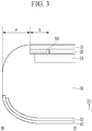
- FIG. 3 is a cross-sectional view taken along line III-III' of FIG. 2
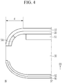
- FIG. 4 is a cross-sectional view taken along line IV-IV' of FIG. 2 .
- a window 10, a display panel 20, and a display device 1 are shown sequentially from the left.
- the window 10 and display panel 20 are shown in a state before bending and lamination.
- the display device 1 includes the window 10 and the display panel 20 laminated (e.g., bonded or attached) onto the window 10, and all four edge areas of the window 10 and the display panel 20 are bent.
- the display device 1 may be an electronic device such as a smartphone, a mobile phone, a tablet, a multimedia player, or a portable information terminal, or may be a module used for such an electronic device. Although not shown, less than all of four edge areas of the window 10 and the display panel 20 may be bent in some cases.
- the Window 10 is a kind of a cover that protects the display panel 20 from external impact.
- the window 10 provides support to maintain the bending state of the display panel 20.
- the window 10 is made of a transparent and hard material such as glass or plastic so as to view an image displayed on the screen of the display panel 20.
- the bending of the window 10 may be performed by thermoforming a glass plate or a plastic plate, for example.
- the display panel 20 may be a light emission display panel including light-emitting elements. At least part of the display panel 20 may be flexible.
- the display panel 20 includes a display area corresponding to a screen on which the image is mostly displayed and a non-display area NA where the image is not displayed. Pixels are arranged in the display area, and the images are displayed by combinations of the pixels.
- signal lines for transmitting signals to drive the pixels are arranged. For example, data signal lines transmitting data signals may extend in the first direction D1, and scan signal lines transmitting scan signals may extend in the second direction D2.
- Each pixel includes a transistor connected to the data signal line and the scan signal line, thereby receiving the data signal controlling a luminance of the pixel at predetermined timing.
- the non-display area NA may be positioned near the edge of the display panel 20, and may be disposed to surround the display area.
- the non-display area NA is an area where circuits and/or wires for generating and/or transmitting various signals applied to the display area are disposed.
- a pad part including pads for receiving signals from the display panel 20 or outputting signals to the outside of the display panel 20 may be disposed.
- the pad part may be disposed in the non-display area NA of the upper side or lower side edges of the display panel 20, and a flexible printed circuit board (PCB) may be attached to the pad part.
- PCB flexible printed circuit board
- the window 10 and the display panel 20 are bent and laminated.
- an adhesive such as an optically clear adhesive may be used. Accordingly, an adhesive layer may be disposed between the window 10 and the display panel 20.
- the display panel 20 is laminated with the window 10 so that the surface where the screen is viewed faces the window 10.
- the window 10 Before the bending and lamination, the window 10 has a rectangular shape with corner parts cut out.
- the window 10 includes a main window region 110, and a first sub-window region 121, a second sub-window region 122, a third sub-window region 123, and a fourth sub-window region 124 that are disposed in contact with the main window region 110.
- the main window region 110 is approximately rectangular and contains four sides 111-114.
- the window edges WE of four window corner parts WC of the main window region 110 are formed to be rounded.
- the first and third sides 111 and 113 extend in the first direction D1, and the second and fourth sides 112 and 114 extend in the second direction D2.
- the first to fourth sub-window regions 121-124 are regions that are bent at a predetermined curvature with respect to the main window region 110.
- the first to fourth sides 111-114 of the main window region 110 become a reference line for bending the first to fourth sub-window regions 121-124 with respect to the main window region 110.
- the first to fourth sides 111-114 of the main window region 110 are bending start lines of the first to fourth sub-window regions 121-124, and hereinafter are simply referred to as bending lines.
- bending lines In the main window region 110, in addition to an approximate rectangle in which the edges of the corner parts are rounded, it may be an approximate polygon with the corner parts rounded.
- the display panel 20 Before the bending and lamination, the display panel 20 has a rectangular shape with corner parts cut out. When the shape of the display panel 20 is divided into regions, the display panel 20 includes a main panel region 210, and a first sub-panel region 221, a second sub-panel region 222, a third sub-panel region 223, and a fourth sub-panel region 224 that are disposed in contact with the main panel region 210.
- the main panel region 210 is an approximate rectangle, and includes four sides 211-214.
- the panel edges PE of four panel corner parts PC of the main panel region 210 are formed to be rounded.
- the first side and the third side 211 and 213 extend in the first direction D1, and the second side and the fourth side 212 and 214 extend in the second direction D2.
- the first to fourth sub-panel regions 221-224 are regions that are bent by the predetermined curvature with respect to the main panel region 210.
- the first to fourth sides 211-214 of the panel region 210 become a reference line for bending the first to fourth sub-panel regions 221-224 with respect to the main panel region 210.
- the first to fourth sides 211-214 of the main panel region 210 are bending start lines of the first to fourth sub-panel regions 221-224, and hereinafter are simply referred to as bending lines.
- bending lines In the main panel region 210, in addition to an approximate rectangle in which the edges of the corner parts are rounded, it may be an approximate polygonal shape with the corner parts rounded.
- the window 10 and the display panel 20 may have substantially the same shape and size.
- the window 10 may be slightly larger than the display panel 20 overall or in a specific region.
- the display panel 20 may be laminated to the window 10.
- the first to fourth sub-panel regions 221-224 of display panel 20 may be bent.
- the display panel 20 may be laminated to the window 10 in the state in which the first to fourth sub-panel regions 221-224 are bent.
- the first to fourth sub-window regions 121-124 of the window 10 and the first to fourth sub-panel regions 221-224 of the display panel 20 are bent.
- the first sub-window region 121 is bent around a bending axis parallel to the first side 111
- the second sub-window region 122 is bent around a bending axis parallel to the second side 112
- the third sub-window region 123 is bent around a bending axis parallel to the third side 113
- the fourth sub-window region 124 is bent around a bending axis parallel to the fourth side 114.
- the first sub-panel region 221 is bent around a bending axis parallel to the first side 211
- the second sub-panel region 222 is bent around a bending axis parallel to the second side 212
- the third sub-panel region 223 is bent around a bending axis parallel to the third side 213
- the fourth sub-panel region 224 is bent around a bending axis parallel to the fourth side 214.
- the bending axis of the first sub-window region 121 and the bending axis of the first sub-panel region 221 may be the same.
- the bending axis of the second sub-window region 122 and the bending axis of the second sub-panel region 222 may be the same.
- the bending axis of the third sub-window region 123 and the bending axis of the third sub-panel region 223 may be the same.
- the bending axis of the fourth sub-window region 124 and the bending axis of the fourth the sub-panel region 224 may be the same.
- the first to fourth sides 111-114 of the main window region 110 may overlap with the first to fourth sides 211-214 of the main panel region 210, and they may be matched in plan view.
- the inner main window region 110 is a plane surface that is not bent, and the outer first to fourth sub-window regions 121-124 are curved surfaces that are bent.
- the inner main panel region 210 is a plane surface that is not bent, and the outer first to fourth sub-panel regions 221-224 are curved surfaces that are bent.
- a width d of the first to fourth sub-window regions 121-124 after bending is narrower than a width c of the first to fourth sub-window regions 121-124 before bending.
- the width d may be about 1/5 to about 4/5, about 1/4 to about 3/4, or about 1/3 to about 2/3 of the width c.
- the non-display area NA positioned at each edge of the sub-panel regions 221-224 may be bent so as to not be visible or to be almost invisible from the front of display device 1. However, since the main panel region 210 is not bent, the non-display area NA positioned at the edge portions of the corner parts PC of the main panel region 210 may be visible from the front.
- the non-display area NA of the display panel 20 is only shown in a specific region. That is, the non-display area NA may be seen in the edge portions of the four corner parts PC of the main panel region 210 of the display panel 20 and the edge portions of the first to fourth the sub-panel regions 221-224 adjacent thereto, and in the remaining regions, the non-display area NA may not be visible or may be barely visible. Therefore, the screen may occupy most of the region to be visible when viewing the display device 1 from the front, and the screen-to-body ratio (a screen to surface ratio) of the display device 1 may be increased.
- the screen-to-body ratio a screen to surface ratio
- the display device 1 may include a light blocking member disposed at the region corresponding to the non-display area NA of the display panel 20, and the light blocking member may be disposed at the window 10 and/or the display panel 20. As described above, elements such as circuits, wirings, and pads may be disposed in the non-display area NA.
- the light blocking member serves to block the elements of the non-display area NA from being visible or to prevent external light, that is, light incident to the display device 1 from the outside, from being reflected.
- the light blocking member may be disposed between display panel 20 and the window 10 or may be disposed inside display panel 20.
- the light blocking member may be referred to as a black matrix, a printing layer, or the like.
- the window edges WE of the window corner parts WC of the main window region 110 are formed to be rounded.
- the panel edges PE of the panel corner parts PC of the main panel region 210 are also formed to be rounded.
- the window edges WE of the window corner parts WC of the main window region 110 may match the panel edges PE of the panel corner parts PC of the main panel region 210.
- the window corner parts WC are formed larger than the panel corner parts PC, so that the window edges WE may be disposed farther from the center of the display device 1 than the edges PE.
- the edges of the corner parts of the screen corresponding to the panel corner parts PC of the main panel region 210 are formed to be rounded, the user may see the image displayed on the screen more comfortably and increase design sensitivity of the display device 1.
- Each panel corner part PC of the main panel region 210 may not overlap with an intersection (or cross point) CP of extending lines of the adjacent sides of the first to fourth sides 211-214 of the main panel region 210.
- FIG. 2 which is an enlarged view of the upper left corner part of the display device 1, shows the extending line of the first side 211 and the extending line of the second side 212 together.
- the panel corner part PC between the first side 211 and the second side 212 of the main panel region 210 does not overlap the intersection CP of the extending line in the first direction D1 of the first side 211 and the extending line in the second direction D2 of the second side 212, and is spaced apart (or separated) from the intersection CP.
- the panel corner part PC of the main panel region 210 When the panel corner part PC of the main panel region 210 is formed in this way, the bending of the first sub-panel region 221 and the second sub-panel region 222 bending around different bending axes does not affect the panel corner part PC of the main panel region 210. Therefore, the stress of the corner part PC of the main panel region 210 may be prevented, and damage to the circuits, the wirings, the pixels, and the like disposed on the corner part PC may be prevented.
- the laminate of the display panel 20 and the window 10 is coupled to the housing 30.
- the housing 30 is a frame that serves to accommodate and fix the laminate of the display panel 20 and the window 10 and may be made of materials such as metal and plastic.
- the display device 1 is a mobile electronic device such as a smartphone, a controller, a memory, a communication module, a camera, an audio input and output device, a circuit board, a battery, etc. may be disposed inside the housing 30 or may be combined with the housing 30.
- a cover 40 may be coupled to the housing 30, and functional sheets such as waterproof tapes 51 and 52 may be disposed between the display panel 20 and the housing 30 and/or between the cover 40 and the housing 30.
- the housing 30 may be invisible or barely visible in the region except for the four corner parts of the display device 1. This is because the housing 30 is covered by the first to fourth sub-window regions 121-124 of the window 10 in such a region. However, in the corner parts of the display device 1, the housing 30 is disposed in the space between the adjacent first to fourth sub-window regions 121-124, so that the edges of the corner parts of the display device 1 may be formed as a whole to be smooth and rounded.
- the width a of the housing 30 seen from the corner parts of the display device 1 may be the same as or almost the same as the width d of the first to fourth sub-window regions 121-124 after bending.
- the width a of the housing 30 (see FIG. 3 ) becomes a bezel of the display device 1 together with the width b of the non-display area NA near the edge of the panel corner parts PC of the main panel region 210.
- the bezel may mean a region disposed outside the screen without composing the screen in plan view of the display device 1 and may be referred to as a dead space.
- the bezel has the width corresponding to the sum of the width a of the non-display area NA and the width b of the housing 30 and an approximate brow shape or a shape of a donut cut into quarters.
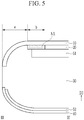
- FIG. 5 a different example of the structure of the corner parts of the display device 1 from the above-described embodiment is shown.
- the housing 30 in the corner part of the display device 1, the housing 30 is disposed in the space between the adjacent first sub-window region 121 and second sub-window region 122 and the housing 30 is exposed in the front.
- the window 10 is formed to cover the housing 30 in the corresponding region. Therefore, in plan view of the display device 1, the corner parts of the display device 1 are covered by the window 10, and the border of the display device 1 and the border of the window 10 may coincide or almost coincide.
- the window 10 is formed like this, the display area of the display panel 20 is not positioned in the corner parts of the display device 1, so the corresponding regions are still the bezel. However, in plan view of the display device 1, since all surfaces are covered by the window 10, a smoother front surface may be formed.
- FIG. 6 is a plan view of a display device according to an embodiment
- FIG. 7 is an enlarged view of one corner part of a display device shown in FIG. 6
- FIG. 8 is cross-sectional view taken along a line VIII-VIII' of FIG. 7 .
- the display device 1 includes the window 10 and the display panel 20 which are bent and laminated, and the housing 30.
- the window 10 includes the main window region 110, and the first to fourth sub-window regions 121-124, which are disposed in contact with the first to fourth sides 111-114 of the main window region 110, respectively, and are bent with a predetermined curvature.
- the first and third side 111 and 113 of the main window region 110 extend in the first direction D1, and the second fourth sides 112 and 114 extend in the second direction D2.
- the first to fourth sides 111-114 are the bending lines of the first to fourth sub-window regions 121-124.
- the edges WE of the corner parts WC in the main window region 110 are formed to be rounded with a predetermined curvature.
- the display panel 20 includes the main panel region 210 and the first to fourth sub-panel regions 221-224, which are disposed in contact with the first to fourth sides 211-214 of the main panel region 210, respectively, and are bent with a predetermined curvature.
- the first and third sides 211, and 213 of the main panel region 210 extend in the first direction D1, and the second and fourth sides 212 and 214 extend in the second direction D2.
- the first to fourth sides 211-214 are the bending lines of the first to fourth sub-panel regions 221-224.
- the panel edges PE of the four panel corner part PCs of the main panel region 210 are formed to be rounded with a predetermined curvature.
- the window 10 and the display panel 20 may have substantially the same shape and size.
- the window edges WE of the window corner parts WC of the main window region 110 may match the edges WE of the panel corner parts PC of the main panel region 210.
- the window edges WE of the window corner parts WC of the main window region 110 may be slightly larger than the panel edges PE of the panel corner parts PC of the main panel region 210.
- the first to fourth sides 111-114 of the main window region 110 may overlap with the first to fourth sides 211-214 of the main panel region 210, and they are flush in plan view.
- the inner main window region 110 is the plane surface that is not bent, and the outer first to fourth sub-window regions 121-124 are the curved surface that is bent based on the bending axis parallel to the first to fourth sides 111-114.
- the inner main panel region 210 is the unbent plane, and the outer first to fourth the sub-panel regions 221-224 are the curved surface bent around the bending axes parallel to the first to fourth sides 211-214.
- the first to fourth sub-window regions 121-124 may be generally curved, but the portions adjacent to the first to fourth sides 111-114 may be the curved surface and the portions far from the first to fourth sides 111-114 may be the plane surface.
- the first to fourth sub-panel regions 221-224 may be entirely curved, but the portions adjacent to the first to fourth sides 211-214 may be the curved surface and the portions farther from the first to fourth sides 211-214 may be the plane surface.
- the non-display area NA disposed on the edge of display panel 20 is invisible or almost invisible from the front of the display device 1 because the first to fourth sub-panel regions 221-224 of the display panel 20 are bent.
- the edge of one corner part of the main panel region 210 and the edges of the adjacent sub-panel regions among the first to fourth sub-panel regions 221-224 form a single curved line without an inflection point.
- the non-display area NA disposed on the edge of one corner part of the main panel region 210 and the non-display area NA disposed on the edges of the adjacent sub-panel regions among the first to fourth sub-panel regions 221-224 form a curved line without the inflection point. For example, referring to FIG.
- the panel edge PE of the upper-left panel corner part PC of the main panel region 210 and the edges of the first sub-panel region 221 and the second sub-panel region 222 adjacent thereto form one curved line C. Therefore, the edges of the corner parts of the display device 1 are formed to be rounded. Also, the non-display area NA forms the curved line of a predetermined width b over the edge PE of the upper-left panel corner part PC of the main panel region 210 and the edges of the first sub-panel region 221 and the second sub-panel region 222 adjacent thereto.
- the edges of the display panel 20 are not connected by one curved line, but are connected by a straight line, a curved line (or an arc), and a straight line.
- the screen of the display panel 20, which is limited by these edges, is not smooth in the corner parts and has a slight sense of incongruity.
- the edges are connected to one curved line in the corner parts of the display panel 20, and the edges of the corner parts of the screen of display panel 20 are formed to be rounded. Therefore, the image displayed on the screen may be viewed comfortably without being awkward, and the design sensitivity of the display device 1 may be further increased.
- first to fourth sub-window regions 121-124 there is no need for the housing 30 to fill the space. Since the first to fourth sub-window regions 121-124 in the corner parts of the display device 1 form the smooth and rounded edge, there is no need to thicken the width a of the housing 30 visible from the front, and it may be formed with the minimum width required for combining with the window 10, for example, as thin as less than 0.5 mm or less than 0.3 mm.
- the width (approximately a+b) of the bezel may be dramatically reduced (e.g., less than about 2 mm, less than about 1.5 mm, or less than about 1 mm), and the screen-to-body ratio of the display device 1 may be increased to close to 100 %.
- the part of the housing 30 constituting the bezel may be in close contact with the corner parts of the window 10, and may be formed to be rounded like the round edges of the corner parts of the window 10 in plan view.
- the housing 30 may not be visible from the front, and only the non-display area NA of the display panel 20 or the region of the window 10 covering the non-display area NA of the display panel 20 may be designed to be the bezel.
- FIG. 7 shows a point of intersection CP where an extension of two adjacent sides among the first to fourth sides 211-214 of the main panel region 210 meet each other. None of the panel corner parts PC of the main panel region 210 coincides with the point of intersection CP.
- the panel corner part PC between the first side 211 and the second side 212 of the main panel region 210 does not coincide with the point of intersection CP where the first side 211 would meet the second side 212 if they were extended in the first direction D1 and the second direction D2, respectively.
- the panel corner part CP is spaced apart from the point of intersection CP.
- the distance between the edge of the panel corner part PC and the point of intersection CP may vary depending on the shape of the corner part PC, but is greater than zero (0).
- the panel corner part PC of the main panel region 210 is formed in this way, the bending of the first sub-panel region 221 and the second sub-panel region 222 bending around the different bending axes does not affect the panel corner part PC of the main panel region 210. Therefore, the stress of the panel corner part PC of the main panel region 210 may be prevented, and the damage of the circuit, wiring, pixels, and the like disposed on the panel corner part PC may be prevented.
- corner part PC of the main panel region 210 may be formed regardless of the bending curvature of the first sub-panel region 221 and the second sub-panel region 222, the design freedom of the corner part PC is increased.
- the explanation uses the upper left panel corner part PC of the main panel region 210 as an example, but the configuration applies to one or more of the upper right, lower left, and lower right corner parts of the main panel region 210.
- each window corner part WC of the main window region 110 may not coincide with the intersection CP where the adjacent sides 111-114 of the first to fourth sides of the main window region 110 would meet if extended.
- the window 10 may include a region overlapping the intersection CP of the extending line of the adjacent sides. Unlike the display panel 20, the window 10 does not include elements such as circuits, wirings, and pads, so there is no risk of damage to such elements even if the biaxial bending at the intersection CP occurs, and this is because the window 10 may be molded three-dimensionally near the point of intersection CP.
- the housing 30 may or may not coincide with the intersection CP of the extending lines of the adjacent sides among the first to fourth sides 111-114 of the main window region 110.
- FIG. 7 depicts the case where the housing 30 does coincide with the intersection CP.
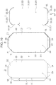
- FIG. 9 to FIG. 14 describe examples of different shapes of the window 10 and the display panel 20 before bending.
- FIG. 9 is a plan view of a window that is built into a display device, a display panel, and a display device according to an embodiment.
- the display device 1 in the state that the window 10 and the display panel 20 are laminated, in plan view, the display device 1 is approximately rectangular, but the edges of the corner parts are rounded.
- the housing that may be combined with the laminate of the display panel 20 and the window 10 may not be visible from the front, and if the size of the window 10 and the display panel 20 is the same, only the non-display area NA of the display panel 20 exists as the bezel in the corner parts of the display device 1.
- the window 10 and the display panel 20 before bending and lamination are the approximate rectangle as a whole, but the edges of the corner parts are rounded.
- the window edge WE of one window corner part WC of the main window region 110 and the edges of the first sub-window region 121 and second sub-window region 122 adjacent thereto form a curved line (or an arc) without an inflection point.
- the panel edge PE of one panel corner part PC of the main panel region 210 and the edges of the first sub-panel region 221 and the second sub-panel region 222 adjacent thereto form a curved line (or the arc) without an inflection point.
- the edges WE of the corner parts WC of the main window region 110 are rounded and the edges PE of the corner parts PC of the main panel region 210 are also rounded.
- the window 10 and the display panel 20 may have the same shape and size.
- the window 10 may be slightly larger than the display panel 20.
- the edges of the corner parts of the display panel 20 are rounded, even if the width of the screen of the display panel 20 (in the display panel 20, the width in the second direction D2 of the region excluding the non-display area NA) changes to the first direction D1, it gradually decreases or increases without a rapid change. For example, as shown in the embodiment of FIG. 1 , if the width of the screen changes rapidly in the corner part of the display panel 20, a load of the signals (e.g., a scan signal, a light emission control signal, and the like) applied to the pixels changes rapidly in the region of the rapid change of the width so that spots may occur in the image displayed on the screen.
- the signals e.g., a scan signal, a light emission control signal, and the like
- a luminance difference may occur in a region before and in a region after the boundary of a line in which the width of the screen changes rapidly, and the luminance difference may be recognized as a spot.
- the width of the screen may be gradually changed to correspond to the shape of the display panel 20, even if the difference in luminance occurs in the region where the width of the screen changes, the difference in luminance is gradual so that it is not recognized as a spot. Therefore, it is possible to provide the display device 1 in which the display is not deteriorated while minimizing the bezel.
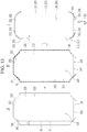
- FIG. 10 is a front view of a window that is built into a display device, a display panel, and a display device according to an embodiment.
- the window 10 and the display panel 20 are the same as the shape remaining after cutting the corner parts from the rectangle into a triangle like chamfering, and the overall shape is approximately octagonal.
- the window 10 and the display panel 20 are overall rectangular, but four corner parts are cut diagonally.
- one window corner part WC of the main window region 110 and the edges of the first sub-window region 121 and the second sub-window region 122 adjacent thereto form a straight line.
- one corner part PC of the main panel region 210 and the edges of the first sub-panel region 221 and the second sub-panel region 222 adjacent thereto form a straight line.
- the panel edges PE of the panel corner parts PC are formed in a straight line, and the first to fourth sub-panel regions 221-224 may be equilateral trapezoids.
- the window edges WE of the window corner parts WC are formed in a straight line, and the first to fourth sub-window regions 121-124 may be equilateral trapezoids.
- the window 10 may have the same shape as the display panel 20, and may be the same as the display panel 20 or slightly larger than the display panel 20.
- the edges of the corner parts of the display panel 20 are formed in an oblique straight line, even if the width of the screen of the display panel 20 changes in the first direction D1, the width does not change rapidly and gradually decreases or increases. Therefore, similar to the embodiment of FIG. 9 , even if a luminance difference occurs in the region where the width of the screen is changed, the luminance difference is gradually increased or decreased, so that the luminance difference is not recognized as a spot.
- the display device 1 is approximately rectangular and the edges of the corner parts may be formed to be rounded.
- the overall shape and the bezel of the display device 1 are the same as described in the embodiment of FIG. 9 .
- FIG. 11 is a plan view of a window that is built into a display device, a display panel, and a display device according to an embodiment
- FIG. 12 is an enlarged view before bending and a cross-sectional view after bending for a lower region in a display panel in FIG. 11 .
- the cross-sectional view after the bending also shows the window.
- the window 10 and the display panel 20 have the shape that would remain after cutting the corner parts off a rectangle.
- the first to fourth sub-panel regions 221-224 are equilateral trapezoids.
- the first and third sub-panel regions 221 and 223 are equilateral trapezoids, and the second and fourth sub-panel regions 222 and 224 have widths that may first gradually decrease with distance from the second and fourth sides 212 and 214 and then remain constant.
- the fourth sub-panel region 224 includes a first portion 224a, which is an equilateral trapezoid, and a second portion 224b, which is a rectangle.
- a pad part may be disposed in the non-display area NA of the second portion 224b. In this way, if the second portion 224b having a constant width is formed, it may be advantageous to secure an area in which the pad part and the signal lines connected to the pad part are disposed, for example.
- the first portion 224a of the fourth sub-panel region 224 may be a curved surface bent around the bending axis BX, and the second portion 224b may be a plane parallel to the third direction D3.
- the curved line formed by the first portion 224a may be an arc corresponding to about a quarter of the circle centered on the bending axis (BX). Accordingly, the screen of the second portion 224b may be perpendicular to the screen of the main panel region 210, and the non-display area NA of the second portion 224b may not be visible from the front of the display device 1.
- the window 10 and display panel 20 when viewing the display device 1 from the front, it is an approximate rectangle and the edges of the four corner parts may be rounded.
- the housing of the display device 1 may not be visible from the front, and if the sizes of the window 10 and the display panel 20 are the same, only the non-display area NA of the display panel 20 exists as the bezel in the corner parts of the display device 1.
- FIG. 13 is a plan view of a window that is built into a display device, a display panel, and a display device according to an embodiment
- FIG. 14 is an enlarged view before bending and a cross-sectional view after bending for a lower region in a display panel in FIG. 13 .
- the cross-section view after bending also shows the window.
- the first to fourth sub-panel regions 221-224 gradually decrease in width farther away from the first to fourth sides 211-214, respectively, and then have a constant shape.
- the fourth sub-panel region 224 includes the first portion 224a, which is an equilateral trapezoid, and the second portion 224b, which is a rectangle. All regions of the second portion 224b may be the non-display area NA. If the second portion 224b having the constant width is formed in this way, it may be advantageous to secure the area where the signal lines connected to the pad part are disposed, for example.
- the first to fourth sub-panel regions 221-224 only the sub-panel region to which the pad part is connected may have this shape, and the remaining sub-panel regions may have a different shape (e.g., the equilateral trapezoid).
- the first portion 224a of the fourth sub-panel region 224 may be a curved surface bent around the bending axis BX, and the second portion 224b may be a plane parallel to the third direction D3.
- the curved line formed by the first portion 224a may be the arc corresponding to about a quarter of the circle centered on the bending axis BX. Accordingly, the non-display area NA of the second portion 224b may not be visible from the front of the display device 1.
- the overall shape and bezel are the same as described in the embodiment of FIG. 9 .
- FIG. 15 is a cross-sectional view showing one example of a lamination structure of the display panel 20 according to an embodiment.
- the cross-section shown in FIG. 15 may correspond to approximately one pixel area.
- the display panel 20 basically includes a substrate SUB, a transistor TR formed on the substrate SUB, and an organic light emitting diode OLED connected to the transistor TR.
- the substrate SUB may be a flexible substrate made of a polymer such as a polyimide, a polyamide, or a polyethylene terephthalate.
- the substrate SUB may include a barrier layer that prevents moisture and oxygen from penetrating from the outside.
- one or more polymer layers and at least one barrier layer may be alternately stacked.
- a first insulating layer IN1 is disposed on the substrate SUB.
- the first insulating layer IN1 may be referred to as a buffer layer, and it blocks an impurity that may diffuse from the substrate SUB to the semiconductor layer A in the process of forming the semiconductor layer A and reduces the stress that the substrate SUB receives.
- the barrier layer and the first insulating layer IN1 may include inorganic insulating materials such as a silicon oxide and a silicon nitride.
- the semiconductor layer A of the transistor TR is disposed on the first insulating layer IN1, and a second insulating layer IN2 is disposed on the semiconductor layer A.
- the semiconductor layer A includes a source region and a drain region, and a channel region between these regions.
- the semiconductor layer A may include a semiconductor material such as a polysilicon, an oxide semiconductor, or amorphous silicon.
- the second insulating layer IN2 may be referred to as a gate insulating layer, and may include an inorganic insulating material.
- a gate conductor including a gate electrode G of the transistor TR is disposed on the second insulating layer IN2.
- the gate conductor may include a metal or metal alloy such as, for example, molybdenum (Mo), copper (Cu), aluminum (Al), silver (Ag), chromium (Cr), tantalum (Ta), and titanium (Ti).
- a third insulating layer IN3 is disposed on the gate conductor.
- the third insulating layer IN3 may be referred to as an interlayer insulating layer, and may include an inorganic insulating material.
- a data conductor including a source electrode S and a drain electrode D of the transistor TR is disposed on the third insulating layer IN3.
- the source electrode S and the drain electrode D are respectively connected to the source region and the drain electrode of the semiconductor layer A through contact holes formed in the third insulating layer IN3 and the second insulating layer IN2.
- the data conductor may include metals or metal alloys such as aluminum (Al), copper (Cu), silver (Ag), molybdenum (Mo), chromium (Cr), gold (Au), platinum (Pt), palladium (Pd), tantalum (Ta), tungsten (W), titanium (Ti), nickel (Ni), and others.
- a fourth insulating layer IN4 is disposed on the data conductor.
- the fourth insulating layer IN4 may be referred to as a passivation layer, a planarization layer, and the like, and may include an organic insulating material.
- a pixel electrode P is disposed on the fourth insulating layer IN4.
- the pixel electrode P is connected to the drain electrode D through a contact hole formed in the fourth insulating layer IN4 to receive a data signal that controls luminance of the organic light emitting diode OLED.
- a fifth insulating layer IN5 is disposed on the fourth insulating layer IN4.
- the fifth insulating layer IN5 may be referred to as a pixel defining layer, and has an opening overlapping the pixel electrode P.
- the emission layer EL is disposed above the pixel electrode P in the opening of the fifth insulating layer IN5, and the common electrode CE is positioned above the emission layer EL.
- the pixel electrode P, the emission layer EL, and the common electrode CE together constitute the organic light emitting diode OLED.
- the pixel electrode P may be an anode of the organic light emitting diode OLED
- the common electrode CE may be a cathode of the organic light emitting diode OLED.
- the common electrode CE can have light transmittance by forming a thin layer of a metal with low work function such as calcium (Ca), barium (Ba), magnesium (Mg), aluminum (Al), and silver (Ag).
- a metal with low work function such as calcium (Ca), barium (Ba), magnesium (Mg), aluminum (Al), and silver (Ag).
- the common electrode CE may be formed of a transparent conductive material such as ITO or IZO.
- An encapsulation layer EC is disposed on the common electrode CE.
- the encapsulation layer EC encapsulates the organic light emitting diode OLED to prevent moisture or oxygen from entering from the outside.
- the encapsulation layer EC may be a thin film encapsulation layer in which an inorganic material layer and/or an organic material layer are stacked.
- a touch sensor layer TS may be disposed on the encapsulation layer EC.
- the touch sensor layer TS may include touch electrodes formed of a transparent conductive material such as ITO or IZO, a metal mesh, or the like, and the touch electrodes may be formed as a single layer or a multilayer.
- An anti-reflection layer (AR) for reducing reflection of external light may be positioned on the touch sensor layer TS.
- the anti-reflection layer AR may include a polarization layer.
- a protective layer to protect the display panel 20 may be disposed on the anti-reflection layer AR.
- a protective layer PF and/or a functional sheet FS for protecting the display panel 20 may be disposed under the substrate SUB.
- the functional sheet FS may include a light shielding sheet, a heating sheet, a waterproof tape, a cushion tape, and the like.
- the display panel 20 is an organic light emitting panel
- the display panel may be various display panels such as a display panel including a light emitting diode (LED) and a display panel including a liquid crystal layer, for example.
- LED light emitting diode
Landscapes
- Physics & Mathematics (AREA)
- Engineering & Computer Science (AREA)
- Nonlinear Science (AREA)
- General Physics & Mathematics (AREA)
- Chemical & Material Sciences (AREA)
- Theoretical Computer Science (AREA)
- Optics & Photonics (AREA)
- Crystallography & Structural Chemistry (AREA)
- Mathematical Physics (AREA)
- General Engineering & Computer Science (AREA)
- Human Computer Interaction (AREA)
- Computer Hardware Design (AREA)
- Inorganic Chemistry (AREA)
- Devices For Indicating Variable Information By Combining Individual Elements (AREA)
- Liquid Crystal (AREA)
Abstract
Description
- This invention relates to a display device.
- Display devices such as an organic light emitting diode display and a liquid crystal display include a display panel on which a screen is positioned. Images are displayed on the screen. The display panels are manufactured by forming several layers and elements on a substrate.
- Glass is used as the substrate of the display panel. However, the glass substrate has drawbacks of being heavy and fragile. In addition, because the glass substrate is rigid, it is difficult to bend the display panel. In recent years, a flexible display panel using a flexible substrate that is lightweight, strong against an impact, and easy to bend and straighten back out has been developed.
- The display panel may have a display area in which most regions form the screen. However, a specific region of the display panel, for example an edge area, may be a non-display area in which a driving circuit, a signal line, etc. are disposed. Typically, the non-display area of the display panel is a limiting factor in increasing a screen-to-body ratio of the display device.
- A display device having an increased screen-to-body ratio is disclosed.
- A display device according to an embodiment includes a display panel and a window laminated with the display panel. The display panel may include: a main panel region including a first side extending in a first direction and a second side extending in a second direction crossing the first direction; a first sub-panel region that is in contact with the first side and is bent; and a second sub-panel region that is in contact with the second side and is bent. A panel corner part of the main panel region adjacent to the first sub-panel region and the second sub-panel region is rounded.
- In plan view, the panel corner part of the main panel region may be spaced apart from an intersection of an extending line of the first side in the first direction and an extending line in the second direction of the second side.
- In plan view, a panel corner part of the display panel including the corner part of the main panel region may be rounded.
- Each of main panel region, the first sub-panel region, and the second sub-panel region may include a display area and a non-display area. In plan view, the non-display area of the first sub-panel region, the non-display area of the main panel, and the non-display area of the second sub-panel region may form a curved line that has no inflection point in the corner part of the display panel.
- The window may include: a main window region including a first side extending in the first direction and a second side extending in the second direction; a first sub-window region in contact with the first side of the main window region; and a second sub-window region in contact with the second side of the main window region. In plan view, a window corner part of the main window region adjacent to the first sub-window region and the second sub-window region may be rounded.
- In plan view, the corner part of the main window region may be spaced apart from an intersection of an extending line in the first direction of the first side of the main window region and an extending line in the second direction of the second side of the main window region.
- The main window region may form a plane, and each of the first sub-window region and the second window region may be bent.
- In plan view, a window corner part of the window including the corner part of the main window region may be rounded.
- The window, the display panel, or the window and the display panel may include a light blocking member at a position corresponding to the non-display area of the main panel region.
- The first side and the second side of the main window region may respectively overlap the first side and the second side of the main panel region.
- The main panel region may further include a third side extending in the first direction and a fourth side extending in the second direction. The display panel may further include a third sub-panel region that is in contact with the third side and is bent, and a second sub-panel region that is in contact with the fourth side and is bent.
- At least one of the first to fourth sub-panel regions may include a first portion that is curved and a second portion that forms a plane.
- A display device according to an embodiment includes a display panel and a window laminated with the display panel. The window includes: a main window region including a first side extending in a first direction and a second side extending in a second direction intersecting the first direction and forming a plane; a first sub-window region that is in contact with the first side and is bent; and a second sub-window region that is in contact with the second side and is bent. A corner part of the main window region adjacent to the first sub-window region and the second sub-window region may be spaced apart from an intersection of an extending line in the first direction of the first side and an extending line in the second direction of the second side.
- In plan view, a window corner part of the main window region may be rounded.
- Each of the first sub-window region and the second sub-window region may include a curved surface.
- In plan view, an edge of a corner part of the window including the corner part of the main window region may be rounded.
- The display device may further include a housing coupled to the window. When viewed from the front of the display device, the housing may be in contact with the edge of the corner part of the window.
- The display panel may include a main panel region, a first sub-panel region in contact with the first side of the main panel region, and a second sub-panel region in contact with the second side of the main panel region. A panel corner part of the main panel region adjacent to the first sub-panel region and the second sub-panel region may non-overlap an intersection of the first side and the second side of the main panel region.
- In plan view, an edge of a corner part of the display panel including the corner part of the main panel region may be rounded.
- A display panel according to an embodiment includes: a main panel region including a first side extending in a first direction and a second side extending in a second direction intersecting the first direction; a first sub-panel region that is in contact with the first side and is bent around a bending axis parallel to the first side; and a second sub-panel region that is in contact with the second side and is bent around a bending axis parallel to the second side. In the display panel, a panel corner part adjacent to the first and second sides may be formed as a curved or straight line before bending of the first and second sub-panel regions, and may be formed in a curve after bending of the first and second sub-panel regions.
- According to embodiments, a display device having almost no bezel and a screen-to-body ratio close to 100 % may be provided. In addition, the bezel may be reduced regardless of the bending curvature of the bending region. In addition, the corner parts of the display device and the edges of the corner parts of the screen are formed as a smooth curved line, which may increase the design sensitivity of the display device.
-
-
FIG. 1 is a plan view of a window that is built into a display device, a display panel, and a display device according to an embodiment. -
FIG. 2 is an enlarged view of one corner part of a display device shown inFIG. 1 . -
FIG. 3 is a cross-sectional view taken along line III-III' ofFIG. 2 . -
FIG. 4 is a cross-sectional view taken along line IV-IV' ofFIG. 2 . -
FIG. 5 is a cross-sectional view of a part corresponding to a line III-III' ofFIG. 2 in a display device according to an embodiment. -
FIG. 6 is a plan view of a display device according to an embodiment. -
FIG. 7 is an enlarged view of one corner part of a display device shown inFIG. 6 . -
FIG. 8 is cross-sectional view taken along a line VIII-VIII' ofFIG. 7 . -
FIG. 9 is a plan view of a window configuring a display device, a display panel, and a display device according to an embodiment. -
FIG. 10 is a plan view of a window configuring a display device, a display panel, and a display device according to an embodiment. -
FIG. 11 is a plan view of a window configuring a display device, a display panel, and a display device according to an embodiment. -
FIG. 12 is an enlarged view before bending and a cross-sectional view after bending for a lower region in a display panel inFIG. 11 . -
FIG. 13 is a plan view of a window configuring a display device, a display panel, and a display device according to an embodiment. -
FIG. 14 is an enlarged view before bending and a cross-sectional view after bending for a lower region in a display panel inFIG. 13 . -
FIG. 15 is a cross-sectional view of a display panel according to an embodiment. - The inventive concept will be described more fully hereinafter with reference to the accompanying drawings, in which embodiments of the inventive concept are shown. As those skilled in the art would realize, the described embodiments may be modified in various different ways, all without departing from the spirit or scope of the inventive concept.
- Like reference numerals designate like elements throughout the specification. In the drawings, the thicknesses or sizes of respective layers and areas may be enlarged or reduced to clearly illustrate their arrangements and relative positions.
- It will be understood that when an element such as a layer, film, region, or substrate is referred to as being "on" another element, it can be directly on the other element or intervening elements may also be present. In contrast, when an element is referred to as being "directly on" another element, there are no intervening elements present.
- In addition, unless explicitly described to the contrary, the word "comprise", and variations such as "comprises" or "comprising", will be understood to imply the inclusion of stated elements but not the exclusion of any other elements.
- Further, in the specification, the phrase "in a plan view" means when an object portion is viewed from the front of a display window or panel, and the phrase "in a cross-sectional view" means when a cross-section taken by vertically cutting an object portion is viewed from the side.
- Now, a display device according to embodiments of the inventive concept is described in detail with reference to accompanying drawings.
-
FIG. 1 is a plan view of a window, a display panel, and a display device according to an embodiment.FIG. 2 is an enlarged view of one corner part of a display device shown inFIG. 1 ,FIG. 3 is a cross-sectional view taken along line III-III' ofFIG. 2 , andFIG. 4 is a cross-sectional view taken along line IV-IV' ofFIG. 2 . - Referring to
FIG. 1 , awindow 10, adisplay panel 20, and adisplay device 1 are shown sequentially from the left. Thewindow 10 anddisplay panel 20 are shown in a state before bending and lamination. Thedisplay device 1 includes thewindow 10 and thedisplay panel 20 laminated (e.g., bonded or attached) onto thewindow 10, and all four edge areas of thewindow 10 and thedisplay panel 20 are bent. Thedisplay device 1 may be an electronic device such as a smartphone, a mobile phone, a tablet, a multimedia player, or a portable information terminal, or may be a module used for such an electronic device. Although not shown, less than all of four edge areas of thewindow 10 and thedisplay panel 20 may be bent in some cases. - The
Window 10 is a kind of a cover that protects thedisplay panel 20 from external impact. Thewindow 10 provides support to maintain the bending state of thedisplay panel 20. Thewindow 10 is made of a transparent and hard material such as glass or plastic so as to view an image displayed on the screen of thedisplay panel 20. The bending of thewindow 10 may be performed by thermoforming a glass plate or a plastic plate, for example. - The
display panel 20 may be a light emission display panel including light-emitting elements. At least part of thedisplay panel 20 may be flexible. Thedisplay panel 20 includes a display area corresponding to a screen on which the image is mostly displayed and a non-display area NA where the image is not displayed. Pixels are arranged in the display area, and the images are displayed by combinations of the pixels. In the display area, signal lines for transmitting signals to drive the pixels are arranged. For example, data signal lines transmitting data signals may extend in the first direction D1, and scan signal lines transmitting scan signals may extend in the second direction D2. Each pixel includes a transistor connected to the data signal line and the scan signal line, thereby receiving the data signal controlling a luminance of the pixel at predetermined timing. - The non-display area NA may be positioned near the edge of the
display panel 20, and may be disposed to surround the display area. The non-display area NA is an area where circuits and/or wires for generating and/or transmitting various signals applied to the display area are disposed. In the non-display area NA, a pad part including pads for receiving signals from thedisplay panel 20 or outputting signals to the outside of thedisplay panel 20 may be disposed. For example, the pad part may be disposed in the non-display area NA of the upper side or lower side edges of thedisplay panel 20, and a flexible printed circuit board (PCB) may be attached to the pad part. - In the
display device 1, thewindow 10 and thedisplay panel 20 are bent and laminated. For the lamination of thewindow 10 anddisplay panel 20, an adhesive such as an optically clear adhesive may be used. Accordingly, an adhesive layer may be disposed between thewindow 10 and thedisplay panel 20. Thedisplay panel 20 is laminated with thewindow 10 so that the surface where the screen is viewed faces thewindow 10. - Before the bending and lamination, the
window 10 has a rectangular shape with corner parts cut out. When the shape of thewindow 10 is divided into regions, thewindow 10 includes amain window region 110, and a firstsub-window region 121, a secondsub-window region 122, a thirdsub-window region 123, and a fourthsub-window region 124 that are disposed in contact with themain window region 110. - The
main window region 110 is approximately rectangular and contains four sides 111-114. The window edges WE of four window corner parts WC of themain window region 110 are formed to be rounded. The first andthird sides fourth sides main window region 110. The first to fourth sides 111-114 of themain window region 110 become a reference line for bending the first to fourth sub-window regions 121-124 with respect to themain window region 110. The first to fourth sides 111-114 of themain window region 110 are bending start lines of the first to fourth sub-window regions 121-124, and hereinafter are simply referred to as bending lines. In themain window region 110, in addition to an approximate rectangle in which the edges of the corner parts are rounded, it may be an approximate polygon with the corner parts rounded. - Before the bending and lamination, the
display panel 20 has a rectangular shape with corner parts cut out. When the shape of thedisplay panel 20 is divided into regions, thedisplay panel 20 includes amain panel region 210, and a firstsub-panel region 221, a secondsub-panel region 222, a thirdsub-panel region 223, and a fourthsub-panel region 224 that are disposed in contact with themain panel region 210. - The
main panel region 210 is an approximate rectangle, and includes four sides 211-214. The panel edges PE of four panel corner parts PC of themain panel region 210 are formed to be rounded. The first side and thethird side fourth side main panel region 210. The first to fourth sides 211-214 of thepanel region 210 become a reference line for bending the first to fourth sub-panel regions 221-224 with respect to themain panel region 210. The first to fourth sides 211-214 of themain panel region 210 are bending start lines of the first to fourth sub-panel regions 221-224, and hereinafter are simply referred to as bending lines. In themain panel region 210, in addition to an approximate rectangle in which the edges of the corner parts are rounded, it may be an approximate polygonal shape with the corner parts rounded. - The
window 10 and thedisplay panel 20 may have substantially the same shape and size. Thewindow 10 may be slightly larger than thedisplay panel 20 overall or in a specific region. After bending the first to fourth sub-window regions 121-124 of thewindow 10, thedisplay panel 20 may be laminated to thewindow 10. During the lamination of thedisplay panel 20, the first to fourth sub-panel regions 221-224 ofdisplay panel 20 may be bent. Alternatively, thedisplay panel 20 may be laminated to thewindow 10 in the state in which the first to fourth sub-panel regions 221-224 are bent. - Referring to
FIG. 1 to FIG. 4 , when thewindow 10 and thedisplay panel 20 are laminated, the first to fourth sub-window regions 121-124 of thewindow 10 and the first to fourth sub-panel regions 221-224 of thedisplay panel 20 are bent. The firstsub-window region 121 is bent around a bending axis parallel to thefirst side 111, the secondsub-window region 122 is bent around a bending axis parallel to thesecond side 112, the thirdsub-window region 123 is bent around a bending axis parallel to thethird side 113, and the fourthsub-window region 124 is bent around a bending axis parallel to thefourth side 114. The firstsub-panel region 221 is bent around a bending axis parallel to thefirst side 211, the secondsub-panel region 222 is bent around a bending axis parallel to thesecond side 212, the thirdsub-panel region 223 is bent around a bending axis parallel to thethird side 213, and the fourthsub-panel region 224 is bent around a bending axis parallel to thefourth side 214. - The bending axis of the first
sub-window region 121 and the bending axis of the firstsub-panel region 221 may be the same. The bending axis of the secondsub-window region 122 and the bending axis of the secondsub-panel region 222 may be the same. The bending axis of the thirdsub-window region 123 and the bending axis of the thirdsub-panel region 223 may be the same. The bending axis of the fourthsub-window region 124 and the bending axis of the fourth thesub-panel region 224 may be the same. The first to fourth sides 111-114 of themain window region 110 may overlap with the first to fourth sides 211-214 of themain panel region 210, and they may be matched in plan view. - In the
window 10, with respect to the boundary of the first to fourth sides 111-114 of themain window region 110, the innermain window region 110 is a plane surface that is not bent, and the outer first to fourth sub-window regions 121-124 are curved surfaces that are bent. Likewise, in thedisplay panel 20, with respect to the boundary of the first to fourth sides 211-214 of themain panel region 210, the innermain panel region 210 is a plane surface that is not bent, and the outer first to fourth sub-panel regions 221-224 are curved surfaces that are bent. A width d of the first to fourth sub-window regions 121-124 after bending is narrower than a width c of the first to fourth sub-window regions 121-124 before bending. For example, the width d may be about 1/5 to about 4/5, about 1/4 to about 3/4, or about 1/3 to about 2/3 of the width c. - In the first to fourth sub-panel regions 221-224, for example as shown in
FIG. 4 , the non-display area NA positioned at each edge of the sub-panel regions 221-224 may be bent so as to not be visible or to be almost invisible from the front ofdisplay device 1. However, since themain panel region 210 is not bent, the non-display area NA positioned at the edge portions of the corner parts PC of themain panel region 210 may be visible from the front. - Like the present embodiment, if the
display panel 20 and thewindow 10 protecting thedisplay panel 20 and the first to fourth sub-window regions 121-124 and the first to fourth the sub-panel regions 221-224 are bent, in plan view of thedisplay device 1, the non-display area NA of thedisplay panel 20 is only shown in a specific region. That is, the non-display area NA may be seen in the edge portions of the four corner parts PC of themain panel region 210 of thedisplay panel 20 and the edge portions of the first to fourth the sub-panel regions 221-224 adjacent thereto, and in the remaining regions, the non-display area NA may not be visible or may be barely visible. Therefore, the screen may occupy most of the region to be visible when viewing thedisplay device 1 from the front, and the screen-to-body ratio (a screen to surface ratio) of thedisplay device 1 may be increased. - The
display device 1 may include a light blocking member disposed at the region corresponding to the non-display area NA of thedisplay panel 20, and the light blocking member may be disposed at thewindow 10 and/or thedisplay panel 20. As described above, elements such as circuits, wirings, and pads may be disposed in the non-display area NA. The light blocking member serves to block the elements of the non-display area NA from being visible or to prevent external light, that is, light incident to thedisplay device 1 from the outside, from being reflected. The light blocking member may be disposed betweendisplay panel 20 and thewindow 10 or may be disposed insidedisplay panel 20. The light blocking member may be referred to as a black matrix, a printing layer, or the like. - The window edges WE of the window corner parts WC of the
main window region 110 are formed to be rounded. The panel edges PE of the panel corner parts PC of themain panel region 210 are also formed to be rounded. The window edges WE of the window corner parts WC of themain window region 110 may match the panel edges PE of the panel corner parts PC of themain panel region 210. In contrast, the window corner parts WC are formed larger than the panel corner parts PC, so that the window edges WE may be disposed farther from the center of thedisplay device 1 than the edges PE. - Since the edges of the corner parts of the screen corresponding to the panel corner parts PC of the
main panel region 210 are formed to be rounded, the user may see the image displayed on the screen more comfortably and increase design sensitivity of thedisplay device 1. - Each panel corner part PC of the
main panel region 210 may not overlap with an intersection (or cross point) CP of extending lines of the adjacent sides of the first to fourth sides 211-214 of themain panel region 210.FIG. 2 , which is an enlarged view of the upper left corner part of thedisplay device 1, shows the extending line of thefirst side 211 and the extending line of thesecond side 212 together. Referring toFIG. 2 , the panel corner part PC between thefirst side 211 and thesecond side 212 of themain panel region 210 does not overlap the intersection CP of the extending line in the first direction D1 of thefirst side 211 and the extending line in the second direction D2 of thesecond side 212, and is spaced apart (or separated) from the intersection CP. When the panel corner part PC of themain panel region 210 is formed in this way, the bending of the firstsub-panel region 221 and the secondsub-panel region 222 bending around different bending axes does not affect the panel corner part PC of themain panel region 210. Therefore, the stress of the corner part PC of themain panel region 210 may be prevented, and damage to the circuits, the wirings, the pixels, and the like disposed on the corner part PC may be prevented. - The laminate of the
display panel 20 and thewindow 10 is coupled to thehousing 30. Thehousing 30 is a frame that serves to accommodate and fix the laminate of thedisplay panel 20 and thewindow 10 and may be made of materials such as metal and plastic. When thedisplay device 1 is a mobile electronic device such as a smartphone, a controller, a memory, a communication module, a camera, an audio input and output device, a circuit board, a battery, etc. may be disposed inside thehousing 30 or may be combined with thehousing 30. On the back of thedisplay device 1, acover 40 may be coupled to thehousing 30, and functional sheets such aswaterproof tapes display panel 20 and thehousing 30 and/or between thecover 40 and thehousing 30. - In plan view (as in
FIG. 2 ), thehousing 30 may be invisible or barely visible in the region except for the four corner parts of thedisplay device 1. This is because thehousing 30 is covered by the first to fourth sub-window regions 121-124 of thewindow 10 in such a region. However, in the corner parts of thedisplay device 1, thehousing 30 is disposed in the space between the adjacent first to fourth sub-window regions 121-124, so that the edges of the corner parts of thedisplay device 1 may be formed as a whole to be smooth and rounded. - The width a of the
housing 30 seen from the corner parts of thedisplay device 1 may be the same as or almost the same as the width d of the first to fourth sub-window regions 121-124 after bending. The width a of the housing 30 (seeFIG. 3 ) becomes a bezel of thedisplay device 1 together with the width b of the non-display area NA near the edge of the panel corner parts PC of themain panel region 210. In this specification, the bezel may mean a region disposed outside the screen without composing the screen in plan view of thedisplay device 1 and may be referred to as a dead space. Therefore, there is little or no bezel in the region except for the corner parts of thedisplay device 1, however in the corner parts of thedisplay device 1, as shown for example, there may be the bezel that has the width corresponding to the sum of the width a of the non-display area NA and the width b of thehousing 30 and an approximate brow shape or a shape of a donut cut into quarters. - Referring to
FIG. 5 , a different example of the structure of the corner parts of thedisplay device 1 from the above-described embodiment is shown. For example, referring toFIG. 2 andFIG. 3 , in the corner part of thedisplay device 1, thehousing 30 is disposed in the space between the adjacent firstsub-window region 121 and secondsub-window region 122 and thehousing 30 is exposed in the front. In contrast, in the embodiment ofFIG. 5 , thewindow 10 is formed to cover thehousing 30 in the corresponding region. Therefore, in plan view of thedisplay device 1, the corner parts of thedisplay device 1 are covered by thewindow 10, and the border of thedisplay device 1 and the border of thewindow 10 may coincide or almost coincide. Even if thewindow 10 is formed like this, the display area of thedisplay panel 20 is not positioned in the corner parts of thedisplay device 1, so the corresponding regions are still the bezel. However, in plan view of thedisplay device 1, since all surfaces are covered by thewindow 10, a smoother front surface may be formed. - Until now, the embodiments in which there is little or no bezel in the regions other than the corner parts of the
display device 1 were described. Hereinafter, an embodiment in which the corner parts of thedisplay device 1 have almost no bezel is described. In order to avoid the complexity of the specification, the descriptions of the same configurations and features as those of the above-described embodiment are simplified or omitted. -
FIG. 6 is a plan view of a display device according to an embodiment,FIG. 7 is an enlarged view of one corner part of a display device shown inFIG. 6 , andFIG. 8 is cross-sectional view taken along a line VIII-VIII' ofFIG. 7 . - Referring to
FIG. 6 to FIG. 8 , thedisplay device 1 includes thewindow 10 and thedisplay panel 20 which are bent and laminated, and thehousing 30. - The
window 10 includes themain window region 110, and the first to fourth sub-window regions 121-124, which are disposed in contact with the first to fourth sides 111-114 of themain window region 110, respectively, and are bent with a predetermined curvature. The first andthird side main window region 110 extend in the first direction D1, and the secondfourth sides main window region 110 are formed to be rounded with a predetermined curvature. - The
display panel 20 includes themain panel region 210 and the first to fourth sub-panel regions 221-224, which are disposed in contact with the first to fourth sides 211-214 of themain panel region 210, respectively, and are bent with a predetermined curvature. The first andthird sides main panel region 210 extend in the first direction D1, and the second andfourth sides main panel region 210 are formed to be rounded with a predetermined curvature. - The
window 10 and thedisplay panel 20 may have substantially the same shape and size. The window edges WE of the window corner parts WC of themain window region 110 may match the edges WE of the panel corner parts PC of themain panel region 210. Although not explicitly shown, the window edges WE of the window corner parts WC of themain window region 110 may be slightly larger than the panel edges PE of the panel corner parts PC of themain panel region 210. The first to fourth sides 111-114 of themain window region 110 may overlap with the first to fourth sides 211-214 of themain panel region 210, and they are flush in plan view. - In the
window 10, with respect to the boundaries of the first to fourth sides 111-114 of themain window region 110, the innermain window region 110 is the plane surface that is not bent, and the outer first to fourth sub-window regions 121-124 are the curved surface that is bent based on the bending axis parallel to the first to fourth sides 111-114. Similarly, when thedisplay panel 20 borders the first to fourth sides 211-214 of themain panel region 210, the innermain panel region 210 is the unbent plane, and the outer first to fourth the sub-panel regions 221-224 are the curved surface bent around the bending axes parallel to the first to fourth sides 211-214. - The first to fourth sub-window regions 121-124 may be generally curved, but the portions adjacent to the first to fourth sides 111-114 may be the curved surface and the portions far from the first to fourth sides 111-114 may be the plane surface. The first to fourth sub-panel regions 221-224 may be entirely curved, but the portions adjacent to the first to fourth sides 211-214 may be the curved surface and the portions farther from the first to fourth sides 211-214 may be the plane surface.
- The non-display area NA disposed on the edge of
display panel 20 is invisible or almost invisible from the front of thedisplay device 1 because the first to fourth sub-panel regions 221-224 of thedisplay panel 20 are bent. In plan view, in the corner parts of thedisplay device 1, the edge of one corner part of themain panel region 210 and the edges of the adjacent sub-panel regions among the first to fourth sub-panel regions 221-224 form a single curved line without an inflection point. In addition, the non-display area NA disposed on the edge of one corner part of themain panel region 210 and the non-display area NA disposed on the edges of the adjacent sub-panel regions among the first to fourth sub-panel regions 221-224 form a curved line without the inflection point. For example, referring toFIG. 7 , the panel edge PE of the upper-left panel corner part PC of themain panel region 210 and the edges of the firstsub-panel region 221 and the secondsub-panel region 222 adjacent thereto form one curved line C. Therefore, the edges of the corner parts of thedisplay device 1 are formed to be rounded. Also, the non-display area NA forms the curved line of a predetermined width b over the edge PE of the upper-left panel corner part PC of themain panel region 210 and the edges of the firstsub-panel region 221 and the secondsub-panel region 222 adjacent thereto. - In the embodiment of
FIG. 1 , in the corner parts of thedisplay device 1, the edges of thedisplay panel 20 are not connected by one curved line, but are connected by a straight line, a curved line (or an arc), and a straight line. The screen of thedisplay panel 20, which is limited by these edges, is not smooth in the corner parts and has a slight sense of incongruity. In the present embodiment, the edges are connected to one curved line in the corner parts of thedisplay panel 20, and the edges of the corner parts of the screen ofdisplay panel 20 are formed to be rounded. Therefore, the image displayed on the screen may be viewed comfortably without being awkward, and the design sensitivity of thedisplay device 1 may be further increased. - On the corner parts of the
display device 1, a portion of thehousing 30 that fixes the laminate of thewindow 10 and thedisplay panel 20 may be seen from the front of thedisplay device 1. However, in the present embodiment, there is no space between adjacent first to fourth sub-window regions 121-124, so there is no need for thehousing 30 to fill the space. Since the first to fourth sub-window regions 121-124 in the corner parts of thedisplay device 1 form the smooth and rounded edge, there is no need to thicken the width a of thehousing 30 visible from the front, and it may be formed with the minimum width required for combining with thewindow 10, for example, as thin as less than 0.5 mm or less than 0.3 mm. Therefore, even if the bezel exists in the four corner parts of thedisplay device 1, the width (approximately a+b) of the bezel may be dramatically reduced (e.g., less than about 2 mm, less than about 1.5 mm, or less than about 1 mm), and the screen-to-body ratio of thedisplay device 1 may be increased to close to 100 %. The part of thehousing 30 constituting the bezel may be in close contact with the corner parts of thewindow 10, and may be formed to be rounded like the round edges of the corner parts of thewindow 10 in plan view. - On the other hand, the
housing 30 may not be visible from the front, and only the non-display area NA of thedisplay panel 20 or the region of thewindow 10 covering the non-display area NA of thedisplay panel 20 may be designed to be the bezel. -
FIG. 7 shows a point of intersection CP where an extension of two adjacent sides among the first to fourth sides 211-214 of themain panel region 210 meet each other. None of the panel corner parts PC of themain panel region 210 coincides with the point of intersection CP. For example, referring toFIG. 7 , the panel corner part PC between thefirst side 211 and thesecond side 212 of themain panel region 210 does not coincide with the point of intersection CP where thefirst side 211 would meet thesecond side 212 if they were extended in the first direction D1 and the second direction D2, respectively. In other words, the panel corner part CP is spaced apart from the point of intersection CP. The distance between the edge of the panel corner part PC and the point of intersection CP may vary depending on the shape of the corner part PC, but is greater than zero (0). When the panel corner part PC of themain panel region 210 is formed in this way, the bending of the firstsub-panel region 221 and the secondsub-panel region 222 bending around the different bending axes does not affect the panel corner part PC of themain panel region 210. Therefore, the stress of the panel corner part PC of themain panel region 210 may be prevented, and the damage of the circuit, wiring, pixels, and the like disposed on the panel corner part PC may be prevented. In addition, since the corner part PC of themain panel region 210 may be formed regardless of the bending curvature of the firstsub-panel region 221 and the secondsub-panel region 222, the design freedom of the corner part PC is increased. The explanation uses the upper left panel corner part PC of themain panel region 210 as an example, but the configuration applies to one or more of the upper right, lower left, and lower right corner parts of themain panel region 210. - In some embodiments, similarly to the
main panel region 210, each window corner part WC of themain window region 110 may not coincide with the intersection CP where the adjacent sides 111-114 of the first to fourth sides of themain window region 110 would meet if extended. However, in other embodiments, thewindow 10 may include a region overlapping the intersection CP of the extending line of the adjacent sides. Unlike thedisplay panel 20, thewindow 10 does not include elements such as circuits, wirings, and pads, so there is no risk of damage to such elements even if the biaxial bending at the intersection CP occurs, and this is because thewindow 10 may be molded three-dimensionally near the point of intersection CP. - The
housing 30 may or may not coincide with the intersection CP of the extending lines of the adjacent sides among the first to fourth sides 111-114 of themain window region 110.FIG. 7 depicts the case where thehousing 30 does coincide with the intersection CP. - As shown above, the
display device 1 of which the edges of the corner parts of thedisplay device 1 are rounded and has almost no bezel may be formed.FIG. 9 to FIG. 14 describe examples of different shapes of thewindow 10 and thedisplay panel 20 before bending. -
FIG. 9 is a plan view of a window that is built into a display device, a display panel, and a display device according to an embodiment. - Referring to
FIG. 9 , in the state that thewindow 10 and thedisplay panel 20 are laminated, in plan view, thedisplay device 1 is approximately rectangular, but the edges of the corner parts are rounded. The housing that may be combined with the laminate of thedisplay panel 20 and thewindow 10 may not be visible from the front, and if the size of thewindow 10 and thedisplay panel 20 is the same, only the non-display area NA of thedisplay panel 20 exists as the bezel in the corner parts of thedisplay device 1. - The
window 10 and thedisplay panel 20 before bending and lamination are the approximate rectangle as a whole, but the edges of the corner parts are rounded. For example, the window edge WE of one window corner part WC of themain window region 110 and the edges of the firstsub-window region 121 and secondsub-window region 122 adjacent thereto form a curved line (or an arc) without an inflection point. In addition, the panel edge PE of one panel corner part PC of themain panel region 210 and the edges of the firstsub-panel region 221 and the secondsub-panel region 222 adjacent thereto form a curved line (or the arc) without an inflection point. The edges WE of the corner parts WC of themain window region 110 are rounded and the edges PE of the corner parts PC of themain panel region 210 are also rounded. Thewindow 10 and thedisplay panel 20 may have the same shape and size. Thewindow 10 may be slightly larger than thedisplay panel 20. - Because the edges of the corner parts of the
display panel 20 are rounded, even if the width of the screen of the display panel 20 (in thedisplay panel 20, the width in the second direction D2 of the region excluding the non-display area NA) changes to the first direction D1, it gradually decreases or increases without a rapid change. For example, as shown in the embodiment ofFIG. 1 , if the width of the screen changes rapidly in the corner part of thedisplay panel 20, a load of the signals (e.g., a scan signal, a light emission control signal, and the like) applied to the pixels changes rapidly in the region of the rapid change of the width so that spots may occur in the image displayed on the screen. That is, a luminance difference may occur in a region before and in a region after the boundary of a line in which the width of the screen changes rapidly, and the luminance difference may be recognized as a spot. According to the present embodiment, since the width of the screen may be gradually changed to correspond to the shape of thedisplay panel 20, even if the difference in luminance occurs in the region where the width of the screen changes, the difference in luminance is gradual so that it is not recognized as a spot. Therefore, it is possible to provide thedisplay device 1 in which the display is not deteriorated while minimizing the bezel. -
FIG. 10 is a front view of a window that is built into a display device, a display panel, and a display device according to an embodiment. - Referring to
FIG. 10 , in the state before the bending and lamination, thewindow 10 and thedisplay panel 20 are the same as the shape remaining after cutting the corner parts from the rectangle into a triangle like chamfering, and the overall shape is approximately octagonal. In other words, thewindow 10 and thedisplay panel 20 are overall rectangular, but four corner parts are cut diagonally. For example, one window corner part WC of themain window region 110 and the edges of the firstsub-window region 121 and the secondsub-window region 122 adjacent thereto form a straight line. In addition, one corner part PC of themain panel region 210 and the edges of the firstsub-panel region 221 and the secondsub-panel region 222 adjacent thereto form a straight line. - In the
main panel region 210, the panel edges PE of the panel corner parts PC are formed in a straight line, and the first to fourth sub-panel regions 221-224 may be equilateral trapezoids. In themain window region 110, the window edges WE of the window corner parts WC are formed in a straight line, and the first to fourth sub-window regions 121-124 may be equilateral trapezoids. Thewindow 10 may have the same shape as thedisplay panel 20, and may be the same as thedisplay panel 20 or slightly larger than thedisplay panel 20. - Since the edges of the corner parts of the
display panel 20 are formed in an oblique straight line, even if the width of the screen of thedisplay panel 20 changes in the first direction D1, the width does not change rapidly and gradually decreases or increases. Therefore, similar to the embodiment ofFIG. 9 , even if a luminance difference occurs in the region where the width of the screen is changed, the luminance difference is gradually increased or decreased, so that the luminance difference is not recognized as a spot. - Even if the edges of the corner parts of the
window 10 and thedisplay panel 20 are straight lines before being bent, they appear round when viewed from the front after bending. Therefore, in the state that thewindow 10 and thedisplay panel 20 are laminated, in plan view, similarly to the embodiment ofFIG. 9 , thedisplay device 1 is approximately rectangular and the edges of the corner parts may be formed to be rounded. The overall shape and the bezel of thedisplay device 1 are the same as described in the embodiment ofFIG. 9 . -
FIG. 11 is a plan view of a window that is built into a display device, a display panel, and a display device according to an embodiment, andFIG. 12 is an enlarged view before bending and a cross-sectional view after bending for a lower region in a display panel inFIG. 11 . InFIG. 12 , the cross-sectional view after the bending also shows the window. - Referring to
FIG. 11 andFIG. 12 , in the state before the bending and lamination, thewindow 10 and thedisplay panel 20 have the shape that would remain after cutting the corner parts off a rectangle. In the case of the embodiment ofFIG. 10 , the first to fourth sub-panel regions 221-224 are equilateral trapezoids. In the present embodiment ofFIG. 11 andFIG. 12 , the first and thirdsub-panel regions sub-panel regions fourth sides sub-panel region 224 includes afirst portion 224a, which is an equilateral trapezoid, and asecond portion 224b, which is a rectangle. A pad part may be disposed in the non-display area NA of thesecond portion 224b. In this way, if thesecond portion 224b having a constant width is formed, it may be advantageous to secure an area in which the pad part and the signal lines connected to the pad part are disposed, for example. - After bending of the
display panel 20, thefirst portion 224a of the fourthsub-panel region 224 may be a curved surface bent around the bending axis BX, and thesecond portion 224b may be a plane parallel to the third direction D3. In the cross-sectional diagram ofFIG. 12 , the curved line formed by thefirst portion 224a may be an arc corresponding to about a quarter of the circle centered on the bending axis (BX). Accordingly, the screen of thesecond portion 224b may be perpendicular to the screen of themain panel region 210, and the non-display area NA of thesecond portion 224b may not be visible from the front of thedisplay device 1. In addition, in the state that thewindow 10 anddisplay panel 20 are laminated, when viewing thedisplay device 1 from the front, it is an approximate rectangle and the edges of the four corner parts may be rounded. The housing of thedisplay device 1 may not be visible from the front, and if the sizes of thewindow 10 and thedisplay panel 20 are the same, only the non-display area NA of thedisplay panel 20 exists as the bezel in the corner parts of thedisplay device 1. -
FIG. 13 is a plan view of a window that is built into a display device, a display panel, and a display device according to an embodiment, andFIG. 14 is an enlarged view before bending and a cross-sectional view after bending for a lower region in a display panel inFIG. 13 . InFIG. 14 , the cross-section view after bending also shows the window. - In the present embodiment, the first to fourth sub-panel regions 221-224 gradually decrease in width farther away from the first to fourth sides 211-214, respectively, and then have a constant shape. For example, the fourth
sub-panel region 224 includes thefirst portion 224a, which is an equilateral trapezoid, and thesecond portion 224b, which is a rectangle. All regions of thesecond portion 224b may be the non-display area NA. If thesecond portion 224b having the constant width is formed in this way, it may be advantageous to secure the area where the signal lines connected to the pad part are disposed, for example. Among the first to fourth sub-panel regions 221-224, only the sub-panel region to which the pad part is connected may have this shape, and the remaining sub-panel regions may have a different shape (e.g., the equilateral trapezoid). - After bending of the
display panel 20, thefirst portion 224a of the fourthsub-panel region 224 may be a curved surface bent around the bending axis BX, and thesecond portion 224b may be a plane parallel to the third direction D3. In the cross-sectional view ofFIG. 14 , the curved line formed by thefirst portion 224a may be the arc corresponding to about a quarter of the circle centered on the bending axis BX. Accordingly, the non-display area NA of thesecond portion 224b may not be visible from the front of thedisplay device 1. When viewing thedisplay device 1 from the front (in plan view), the overall shape and bezel are the same as described in the embodiment ofFIG. 9 . - In the following, the cross-sectional structure of the
display panel 20 is described in detail with reference toFIG. 15 . -
FIG. 15 is a cross-sectional view showing one example of a lamination structure of thedisplay panel 20 according to an embodiment. The cross-section shown inFIG. 15 may correspond to approximately one pixel area. Thedisplay panel 20 basically includes a substrate SUB, a transistor TR formed on the substrate SUB, and an organic light emitting diode OLED connected to the transistor TR. - The substrate SUB may be a flexible substrate made of a polymer such as a polyimide, a polyamide, or a polyethylene terephthalate. The substrate SUB may include a barrier layer that prevents moisture and oxygen from penetrating from the outside. For example, in the substrate SUB, one or more polymer layers and at least one barrier layer may be alternately stacked.
- A first insulating layer IN1 is disposed on the substrate SUB. The first insulating layer IN1 may be referred to as a buffer layer, and it blocks an impurity that may diffuse from the substrate SUB to the semiconductor layer A in the process of forming the semiconductor layer A and reduces the stress that the substrate SUB receives. The barrier layer and the first insulating layer IN1 may include inorganic insulating materials such as a silicon oxide and a silicon nitride.
- The semiconductor layer A of the transistor TR is disposed on the first insulating layer IN1, and a second insulating layer IN2 is disposed on the semiconductor layer A. The semiconductor layer A includes a source region and a drain region, and a channel region between these regions. The semiconductor layer A may include a semiconductor material such as a polysilicon, an oxide semiconductor, or amorphous silicon. The second insulating layer IN2 may be referred to as a gate insulating layer, and may include an inorganic insulating material.
- A gate conductor including a gate electrode G of the transistor TR is disposed on the second insulating layer IN2. The gate conductor may include a metal or metal alloy such as, for example, molybdenum (Mo), copper (Cu), aluminum (Al), silver (Ag), chromium (Cr), tantalum (Ta), and titanium (Ti).
- A third insulating layer IN3 is disposed on the gate conductor. The third insulating layer IN3 may be referred to as an interlayer insulating layer, and may include an inorganic insulating material.
- A data conductor including a source electrode S and a drain electrode D of the transistor TR is disposed on the third insulating layer IN3. The source electrode S and the drain electrode D are respectively connected to the source region and the drain electrode of the semiconductor layer A through contact holes formed in the third insulating layer IN3 and the second insulating layer IN2. The data conductor, for example, may include metals or metal alloys such as aluminum (Al), copper (Cu), silver (Ag), molybdenum (Mo), chromium (Cr), gold (Au), platinum (Pt), palladium (Pd), tantalum (Ta), tungsten (W), titanium (Ti), nickel (Ni), and others.
- A fourth insulating layer IN4 is disposed on the data conductor. The fourth insulating layer IN4 may be referred to as a passivation layer, a planarization layer, and the like, and may include an organic insulating material.
- A pixel electrode P is disposed on the fourth insulating layer IN4. The pixel electrode P is connected to the drain electrode D through a contact hole formed in the fourth insulating layer IN4 to receive a data signal that controls luminance of the organic light emitting diode OLED.
- A fifth insulating layer IN5 is disposed on the fourth insulating layer IN4. The fifth insulating layer IN5 may be referred to as a pixel defining layer, and has an opening overlapping the pixel electrode P. The emission layer EL is disposed above the pixel electrode P in the opening of the fifth insulating layer IN5, and the common electrode CE is positioned above the emission layer EL. The pixel electrode P, the emission layer EL, and the common electrode CE together constitute the organic light emitting diode OLED. The pixel electrode P may be an anode of the organic light emitting diode OLED, and the common electrode CE may be a cathode of the organic light emitting diode OLED. The common electrode CE can have light transmittance by forming a thin layer of a metal with low work function such as calcium (Ca), barium (Ba), magnesium (Mg), aluminum (Al), and silver (Ag). The common electrode CE may be formed of a transparent conductive material such as ITO or IZO.
- An encapsulation layer EC is disposed on the common electrode CE. The encapsulation layer EC encapsulates the organic light emitting diode OLED to prevent moisture or oxygen from entering from the outside. The encapsulation layer EC may be a thin film encapsulation layer in which an inorganic material layer and/or an organic material layer are stacked.
- A touch sensor layer TS may be disposed on the encapsulation layer EC. The touch sensor layer TS may include touch electrodes formed of a transparent conductive material such as ITO or IZO, a metal mesh, or the like, and the touch electrodes may be formed as a single layer or a multilayer.
- An anti-reflection layer (AR) for reducing reflection of external light may be positioned on the touch sensor layer TS. The anti-reflection layer AR may include a polarization layer. On the anti-reflection layer AR, a protective layer to protect the
display panel 20 may be disposed. - A protective layer PF and/or a functional sheet FS for protecting the
display panel 20 may be disposed under the substrate SUB. The functional sheet FS may include a light shielding sheet, a heating sheet, a waterproof tape, a cushion tape, and the like. - Although the case where the
display panel 20 is an organic light emitting panel has been described as an example, the display panel may be various display panels such as a display panel including a light emitting diode (LED) and a display panel including a liquid crystal layer, for example. - While the inventive concept has been described in connection with what is presently considered to be practical embodiments, it is to be understood that the inventive concept is not limited to the disclosed embodiments. On the contrary, it is intended to cover various modifications and equivalent arrangements included within the spirit and scope of the appended claims.
Claims (20)
- A display device comprising:a display panel and a window laminated with the display panel,wherein the display panel includes:a main panel region including a first side extending in a first direction and a second side extending in a second direction crossing the first direction;a first sub-panel region that is in contact with the first side and is bent; anda second sub-panel region that is in contact with the second side and is bent, andwherein a panel corner part of the main panel region adjacent to the first sub-panel region and the second sub-panel region is rounded.
- The display device of claim 1, wherein
the panel corner part of the main panel region is spaced apart from an intersection of an extending line of the first side in the first direction and an extending line in the second direction of the second side in plan view. - The display device of claim 2, wherein
a panel corner part of the display panel including the corner part of the main panel region is rounded in plan view. - The display device of claim 3, wherein
each of the main panel region, the first sub-panel region, and the second sub-panel region includes a display area and a non-display area, and
the non-display area of the first sub-panel region, the non-display area of the main panel, and the non-display area of the second sub-panel region form a curved line that has no inflection point in the corner part of the display panel in plan view. - The display device of claim 4, wherein
the window includes:a main window region including a first side extending in the first direction and a second side extending in the second direction;a first sub-window region in contact with the first side of the main window region; anda second sub-window region in contact with the second side of the main window region, anda window corner part of the main window region adjacent to the first sub-window region and the second sub-window region is rounded. - The display device of claim 5, wherein
the window corner part of the main window region is spaced apart from an intersection of an extending line in the first direction of the first side of the main window region and an extending line in the second direction of the second side of the main window region in plan view. - The display device of claim 5, wherein
the main window region forms a plane, and each of the first sub-window region and the second window region is bent. - The display device of claim 5, wherein
a window corner part of the window including the corner part of the main window region is rounded in plan view. - The display device of claim 5, wherein
the window, the display panel, or the window and the display panel include a light blocking member at a position corresponding to the non-display area of the main panel region. - The display device of claim 5, wherein
the first side and the second side of the main window region respectively overlap the first side and the second side of the main panel region. - The display device of claim 1, wherein
the main panel region further includes a third side extending in the first direction and a fourth side extending in the second direction, and
the display panel further includes a third sub-panel region that is in contact with the third side and is bent, and a second sub-panel region that is in contact with the fourth side and bent. - The display device of claim 11, wherein
at least one of the first to fourth sub-panel regions includes a first portion that is curved and a second portion that is planar. - A display device comprisinga display panel and a window laminated with the display panel,wherein the window includes:a main window region including a first side extending in a first direction and a second side extending in a second direction intersecting the first direction and forming a plane;a first sub-window region that is in contact with the first side and is bent; anda second sub-window region that is in contact with the second side and is bent, andwherein a corner part of the main window region adjacent to the first sub-window region and the second sub-window region is spaced apart from an intersection of an extending line in the first direction of the first side and an extending line in the second direction of the second side.
- The display device of claim 13, wherein
when viewed from a front of the display device, an edge of the corner part of the main window region is rounded. - The display device of claim 13, wherein
each of the first sub-window region and the second sub-window region includes a curved surface. - The display device of claim 13, wherein
a window corner part of the window including the corner part of the main window region is rounded in plan view. - The display device of claim 16, further comprising:a housing coupled to the window, andthe housing is in contact with the edge of the corner part of the window in plan view.
- The display device of claim 13, wherein
the display panel includes a main panel region, a first sub-panel region in contact with the first side of the main panel region, and a second sub-panel region in contact with the second side of the main panel region,
wherein a panel corner part of the main panel region adjacent to the first sub-panel region and the second sub-panel region is spaced from an intersection of the first side and the second side of the main panel region. - The display device of claim 18, wherein
a corner part of the main panel region is rounded in plan view. - A display panel comprising:a main panel region including a first side extending in a first direction and a second side extending in a second direction intersecting the first direction;a first sub-panel region that is in contact with the first side and is bent around a bending axis parallel to the first side; anda second sub-panel region that is in contact with the second side and is bent around a bending axis parallel to the second side,wherein a panel corner part adjacent to the first and second sides is formed as a curved or straight line before bending of the first and second sub-panel regions and is formed in a curve after bending of the first and second sub-panel regions.
Applications Claiming Priority (2)
| Application Number | Priority Date | Filing Date | Title |
|---|---|---|---|
| KR1020180082185A KR102559524B1 (en) | 2018-07-16 | 2018-07-16 | Display device |
| PCT/KR2019/006436 WO2020017757A1 (en) | 2018-07-16 | 2019-05-29 | Display device |
Publications (2)
| Publication Number | Publication Date |
|---|---|
| EP3825757A1 true EP3825757A1 (en) | 2021-05-26 |
| EP3825757A4 EP3825757A4 (en) | 2022-04-13 |
Family
ID=69164692
Family Applications (1)
| Application Number | Title | Priority Date | Filing Date |
|---|---|---|---|
| EP19838469.5A Pending EP3825757A4 (en) | 2018-07-16 | 2019-05-29 | DISPLAY DEVICE |
Country Status (5)
| Country | Link |
|---|---|
| US (1) | US11940837B2 (en) |
| EP (1) | EP3825757A4 (en) |
| KR (1) | KR102559524B1 (en) |
| CN (1) | CN112424678B (en) |
| WO (1) | WO2020017757A1 (en) |
Families Citing this family (14)
| Publication number | Priority date | Publication date | Assignee | Title |
|---|---|---|---|---|
| USD1044788S1 (en) * | 2019-04-24 | 2024-10-01 | Samsung Display Co., Ltd. | Cover window for a display panel |
| CN111899640B (en) * | 2019-05-06 | 2021-10-26 | 华为技术有限公司 | Electronic equipment with curved surface display screen |
| KR102618250B1 (en) * | 2019-05-13 | 2023-12-29 | 삼성디스플레이 주식회사 | Window member and display device with window member |
| EP4123415B1 (en) * | 2020-03-20 | 2024-05-01 | BOE Technology Group Co., Ltd. | Display device and manufacturing method therefor |
| CN111403453B (en) * | 2020-03-26 | 2023-06-30 | 武汉华星光电半导体显示技术有限公司 | Flexible display panel and display device |
| KR102933779B1 (en) | 2020-05-29 | 2026-03-04 | 삼성디스플레이 주식회사 | Display device and manufacturing method of display device |
| JP7488559B2 (en) * | 2020-07-09 | 2024-05-22 | 株式会社喜多俊之デザイン研究所 | Display device |
| KR20220041272A (en) | 2020-09-24 | 2022-04-01 | 삼성디스플레이 주식회사 | Display device |
| KR102874014B1 (en) * | 2020-10-23 | 2025-10-23 | 삼성디스플레이 주식회사 | Electronic device |
| CN112863366B (en) * | 2021-03-12 | 2022-07-12 | 武汉华星光电半导体显示技术有限公司 | Display panel and display device |
| CN113066366B (en) * | 2021-03-15 | 2022-05-17 | 武汉华星光电半导体显示技术有限公司 | Display panels and display devices |
| CN113140165B (en) * | 2021-04-14 | 2022-07-12 | 武汉华星光电半导体显示技术有限公司 | Display device and manufacturing method thereof |
| KR20230048208A (en) * | 2021-10-01 | 2023-04-11 | 삼성디스플레이 주식회사 | Display apparatus and method for manufacturing the same |
| KR20240076516A (en) * | 2022-11-22 | 2024-05-30 | 엘지디스플레이 주식회사 | Display device |
Family Cites Families (20)
| Publication number | Priority date | Publication date | Assignee | Title |
|---|---|---|---|---|
| KR101212172B1 (en) | 2012-07-31 | 2012-12-13 | 한국기계연구원 | Display device |
| US9250651B2 (en) | 2013-04-24 | 2016-02-02 | Google Technology Holdings LLC | Electronic device with folded display |
| US9430180B2 (en) | 2013-11-15 | 2016-08-30 | Semiconductor Energy Laboratory Co., Ltd | Display panel and electronic device |
| US9379355B1 (en) * | 2014-12-15 | 2016-06-28 | Lg Display Co., Ltd. | Flexible display device having support layer with rounded edge |
| EP3537694B1 (en) | 2015-02-06 | 2023-08-02 | Samsung Electronics Co., Ltd. | Electronic device including display with bent area |
| KR102296846B1 (en) * | 2015-02-06 | 2021-09-01 | 삼성전자주식회사 | Key button assembly and electronic device having it |
| EP3890286B1 (en) | 2015-02-06 | 2023-08-16 | Samsung Electronics Co., Ltd. | Portable electronic device |
| KR20170040440A (en) * | 2015-10-02 | 2017-04-13 | 삼성디스플레이 주식회사 | Display device |
| KR102404370B1 (en) * | 2015-10-02 | 2022-06-03 | 삼성디스플레이 주식회사 | Window and display device having the same |
| KR102442613B1 (en) * | 2015-12-15 | 2022-09-14 | 삼성디스플레이 주식회사 | flexible display device |
| KR102398061B1 (en) | 2016-01-11 | 2022-05-16 | 삼성디스플레이 주식회사 | Flexible display apparatus |
| KR102510396B1 (en) * | 2016-02-12 | 2023-03-16 | 삼성디스플레이 주식회사 | Flexible display apparatus and manufacturing method thereof |
| KR102560703B1 (en) * | 2016-04-29 | 2023-07-28 | 삼성디스플레이 주식회사 | Display apparatus |
| KR102596956B1 (en) | 2016-05-23 | 2023-11-01 | 삼성디스플레이 주식회사 | Display device |
| KR102717102B1 (en) | 2016-09-06 | 2024-10-16 | 삼성디스플레이 주식회사 | Display apparatus |
| KR102653367B1 (en) * | 2016-12-08 | 2024-04-02 | 삼성전자 주식회사 | Electronic device comprising bended display and method for controlling the same |
| CN113534522B (en) | 2016-12-23 | 2025-02-14 | 群创光电股份有限公司 | Display Devices |
| KR101919803B1 (en) | 2017-08-10 | 2018-11-19 | 엘지전자 주식회사 | Mobile terminal |
| CN107784940B (en) | 2017-11-10 | 2019-11-05 | 武汉华星光电半导体显示技术有限公司 | Display panel and display device |
| US10509436B2 (en) | 2017-11-10 | 2019-12-17 | Wuhan China Star Optoelectronics Semiconductor Display Technology Co., Ltd. | Display panel and display device |
-
2018
- 2018-07-16 KR KR1020180082185A patent/KR102559524B1/en active Active
-
2019
- 2019-05-29 US US17/260,971 patent/US11940837B2/en active Active
- 2019-05-29 CN CN201980047426.3A patent/CN112424678B/en active Active
- 2019-05-29 EP EP19838469.5A patent/EP3825757A4/en active Pending
- 2019-05-29 WO PCT/KR2019/006436 patent/WO2020017757A1/en not_active Ceased
Also Published As
| Publication number | Publication date |
|---|---|
| US20210320275A1 (en) | 2021-10-14 |
| WO2020017757A1 (en) | 2020-01-23 |
| CN112424678A (en) | 2021-02-26 |
| US11940837B2 (en) | 2024-03-26 |
| EP3825757A4 (en) | 2022-04-13 |
| KR20200008679A (en) | 2020-01-29 |
| KR102559524B1 (en) | 2023-07-25 |
| CN112424678B (en) | 2025-02-18 |
Similar Documents
| Publication | Publication Date | Title |
|---|---|---|
| US11940837B2 (en) | Display device with higher screen-to-body ratio | |
| US11233112B2 (en) | Display device | |
| US11588001B2 (en) | Display device having an encapsulation layer and power line in non-display area | |
| KR102625708B1 (en) | Display device | |
| CN112018155A (en) | display device | |
| US10657850B2 (en) | Foldable display device | |
| KR20200091529A (en) | Flexible display device | |
| US10304917B2 (en) | Flexible display device | |
| KR20200058638A (en) | Display device and manufacturing method thereof | |
| KR102668620B1 (en) | Foldable Display | |
| KR102668512B1 (en) | Foldable Display | |
| US11316138B2 (en) | Display device and manufacturing method thereof | |
| US20200243781A1 (en) | Display device | |
| KR20190100564A (en) | Display device | |
| US20220231110A1 (en) | Display device | |
| US11508936B2 (en) | Display device including block patterns | |
| US20240074284A1 (en) | Display device | |
| US20250366357A1 (en) | Display panel comprising conductive tape | |
| US20240138238A1 (en) | Display apparatus | |
| US12114452B2 (en) | Display panel | |
| CN113963623A (en) | Display device | |
| KR20230164266A (en) | Display device | |
| US20250374803A1 (en) | Display device including cover window | |
| US20250107416A1 (en) | Display device and method for manufacturing the display device | |
| KR102667252B1 (en) | Flexible Display Device |
Legal Events
| Date | Code | Title | Description |
|---|---|---|---|
| STAA | Information on the status of an ep patent application or granted ep patent |
Free format text: STATUS: THE INTERNATIONAL PUBLICATION HAS BEEN MADE |
|
| PUAI | Public reference made under article 153(3) epc to a published international application that has entered the european phase |
Free format text: ORIGINAL CODE: 0009012 |
|
| STAA | Information on the status of an ep patent application or granted ep patent |
Free format text: STATUS: REQUEST FOR EXAMINATION WAS MADE |
|
| 17P | Request for examination filed |
Effective date: 20210201 |
|
| AK | Designated contracting states |
Kind code of ref document: A1 Designated state(s): AL AT BE BG CH CY CZ DE DK EE ES FI FR GB GR HR HU IE IS IT LI LT LU LV MC MK MT NL NO PL PT RO RS SE SI SK SM TR |
|
| DAV | Request for validation of the european patent (deleted) | ||
| DAX | Request for extension of the european patent (deleted) | ||
| A4 | Supplementary search report drawn up and despatched |
Effective date: 20220311 |
|
| RIC1 | Information provided on ipc code assigned before grant |
Ipc: G06F 1/16 20060101ALI20220305BHEP Ipc: H01L 51/00 20060101ALI20220305BHEP Ipc: H01L 51/52 20060101ALI20220305BHEP Ipc: G02F 1/1333 20060101AFI20220305BHEP |
|
| P01 | Opt-out of the competence of the unified patent court (upc) registered |
Effective date: 20230516 |
|
| STAA | Information on the status of an ep patent application or granted ep patent |
Free format text: STATUS: EXAMINATION IS IN PROGRESS |
|
| 17Q | First examination report despatched |
Effective date: 20240110 |