EP3823014A2 - Devices including radio frequency devices and methods - Google Patents
Devices including radio frequency devices and methods Download PDFInfo
- Publication number
- EP3823014A2 EP3823014A2 EP19209444.9A EP19209444A EP3823014A2 EP 3823014 A2 EP3823014 A2 EP 3823014A2 EP 19209444 A EP19209444 A EP 19209444A EP 3823014 A2 EP3823014 A2 EP 3823014A2
- Authority
- EP
- European Patent Office
- Prior art keywords
- silicon
- filler regions
- radio frequency
- regions
- region
- Prior art date
- Legal status (The legal status is an assumption and is not a legal conclusion. Google has not performed a legal analysis and makes no representation as to the accuracy of the status listed.)
- Granted
Links
Images



Classifications
-
- H—ELECTRICITY
- H10—SEMICONDUCTOR DEVICES; ELECTRIC SOLID-STATE DEVICES NOT OTHERWISE PROVIDED FOR
- H10P—GENERIC PROCESSES OR APPARATUS FOR THE MANUFACTURE OR TREATMENT OF DEVICES COVERED BY CLASS H10
- H10P90/00—Preparation of wafers not covered by a single main group of this subclass, e.g. wafer reinforcement
- H10P90/19—Preparing inhomogeneous wafers
- H10P90/1904—Preparing vertically inhomogeneous wafers
- H10P90/1906—Preparing SOI wafers
-
- H—ELECTRICITY
- H10—SEMICONDUCTOR DEVICES; ELECTRIC SOLID-STATE DEVICES NOT OTHERWISE PROVIDED FOR
- H10D—INORGANIC ELECTRIC SEMICONDUCTOR DEVICES
- H10D86/00—Integrated devices formed in or on insulating or conducting substrates, e.g. formed in silicon-on-insulator [SOI] substrates or on stainless steel or glass substrates
- H10D86/01—Manufacture or treatment
-
- H—ELECTRICITY
- H10—SEMICONDUCTOR DEVICES; ELECTRIC SOLID-STATE DEVICES NOT OTHERWISE PROVIDED FOR
- H10D—INORGANIC ELECTRIC SEMICONDUCTOR DEVICES
- H10D86/00—Integrated devices formed in or on insulating or conducting substrates, e.g. formed in silicon-on-insulator [SOI] substrates or on stainless steel or glass substrates
- H10D86/201—Integrated devices formed in or on insulating or conducting substrates, e.g. formed in silicon-on-insulator [SOI] substrates or on stainless steel or glass substrates the substrates comprising an insulating layer on a semiconductor body, e.g. SOI
-
- H—ELECTRICITY
- H10—SEMICONDUCTOR DEVICES; ELECTRIC SOLID-STATE DEVICES NOT OTHERWISE PROVIDED FOR
- H10P—GENERIC PROCESSES OR APPARATUS FOR THE MANUFACTURE OR TREATMENT OF DEVICES COVERED BY CLASS H10
- H10P36/00—Gettering within semiconductor bodies
- H10P36/03—Gettering within semiconductor bodies within silicon bodies
- H10P36/07—Gettering within semiconductor bodies within silicon bodies of silicon-on-insulator structures
-
- H—ELECTRICITY
- H10—SEMICONDUCTOR DEVICES; ELECTRIC SOLID-STATE DEVICES NOT OTHERWISE PROVIDED FOR
- H10W—GENERIC PACKAGES, INTERCONNECTIONS, CONNECTORS OR OTHER CONSTRUCTIONAL DETAILS OF DEVICES COVERED BY CLASS H10
- H10W10/00—Isolation regions in semiconductor bodies between components of integrated devices
-
- H—ELECTRICITY
- H10—SEMICONDUCTOR DEVICES; ELECTRIC SOLID-STATE DEVICES NOT OTHERWISE PROVIDED FOR
- H10W—GENERIC PACKAGES, INTERCONNECTIONS, CONNECTORS OR OTHER CONSTRUCTIONAL DETAILS OF DEVICES COVERED BY CLASS H10
- H10W10/00—Isolation regions in semiconductor bodies between components of integrated devices
- H10W10/01—Manufacture or treatment
-
- H—ELECTRICITY
- H10—SEMICONDUCTOR DEVICES; ELECTRIC SOLID-STATE DEVICES NOT OTHERWISE PROVIDED FOR
- H10W—GENERIC PACKAGES, INTERCONNECTIONS, CONNECTORS OR OTHER CONSTRUCTIONAL DETAILS OF DEVICES COVERED BY CLASS H10
- H10W10/00—Isolation regions in semiconductor bodies between components of integrated devices
- H10W10/01—Manufacture or treatment
- H10W10/011—Manufacture or treatment of isolation regions comprising dielectric materials
- H10W10/014—Manufacture or treatment of isolation regions comprising dielectric materials using trench refilling with dielectric materials, e.g. shallow trench isolations
-
- H—ELECTRICITY
- H10—SEMICONDUCTOR DEVICES; ELECTRIC SOLID-STATE DEVICES NOT OTHERWISE PROVIDED FOR
- H10W—GENERIC PACKAGES, INTERCONNECTIONS, CONNECTORS OR OTHER CONSTRUCTIONAL DETAILS OF DEVICES COVERED BY CLASS H10
- H10W10/00—Isolation regions in semiconductor bodies between components of integrated devices
- H10W10/01—Manufacture or treatment
- H10W10/041—Manufacture or treatment of isolation regions comprising polycrystalline semiconductor materials
-
- H—ELECTRICITY
- H10—SEMICONDUCTOR DEVICES; ELECTRIC SOLID-STATE DEVICES NOT OTHERWISE PROVIDED FOR
- H10W—GENERIC PACKAGES, INTERCONNECTIONS, CONNECTORS OR OTHER CONSTRUCTIONAL DETAILS OF DEVICES COVERED BY CLASS H10
- H10W10/00—Isolation regions in semiconductor bodies between components of integrated devices
- H10W10/01—Manufacture or treatment
- H10W10/061—Manufacture or treatment using SOI processes together with lateral isolation, e.g. combinations of SOI and shallow trench isolations
-
- H—ELECTRICITY
- H10—SEMICONDUCTOR DEVICES; ELECTRIC SOLID-STATE DEVICES NOT OTHERWISE PROVIDED FOR
- H10W—GENERIC PACKAGES, INTERCONNECTIONS, CONNECTORS OR OTHER CONSTRUCTIONAL DETAILS OF DEVICES COVERED BY CLASS H10
- H10W10/00—Isolation regions in semiconductor bodies between components of integrated devices
- H10W10/10—Isolation regions comprising dielectric materials
- H10W10/17—Isolation regions comprising dielectric materials formed using trench refilling with dielectric materials, e.g. shallow trench isolations
-
- H—ELECTRICITY
- H10—SEMICONDUCTOR DEVICES; ELECTRIC SOLID-STATE DEVICES NOT OTHERWISE PROVIDED FOR
- H10W—GENERIC PACKAGES, INTERCONNECTIONS, CONNECTORS OR OTHER CONSTRUCTIONAL DETAILS OF DEVICES COVERED BY CLASS H10
- H10W10/00—Isolation regions in semiconductor bodies between components of integrated devices
- H10W10/10—Isolation regions comprising dielectric materials
- H10W10/181—Semiconductor-on-insulator [SOI] isolation regions, e.g. buried oxide regions of SOI wafers
-
- H—ELECTRICITY
- H10—SEMICONDUCTOR DEVICES; ELECTRIC SOLID-STATE DEVICES NOT OTHERWISE PROVIDED FOR
- H10W—GENERIC PACKAGES, INTERCONNECTIONS, CONNECTORS OR OTHER CONSTRUCTIONAL DETAILS OF DEVICES COVERED BY CLASS H10
- H10W10/00—Isolation regions in semiconductor bodies between components of integrated devices
- H10W10/40—Isolation regions comprising polycrystalline semiconductor materials
Definitions
- the present application relates to devices including radio frequency (RF) devices and methods related thereto, in particular methods for manufacturing such devices.
- RF radio frequency
- Radio frequency devices are for example used in communication circuits.
- Examples for radio frequency devices are transistor-based radio frequency switches, which in some implementations may be formed by coupling a plurality of transistors in series.
- Other examples may include passive radio frequency devices.
- Radio frequency as used herein, may relate to frequencies above 100 kHz, in particular in the MHz range or GHz range. For example, for the upcoming 5G (5 th generation) mobile communication standard frequencies up to 300 GHz will be used.
- radio frequency devices are manufactured on silicon on insulator (SOI) substrates.
- a method comprising:
- a method comprising:
- a device comprising:
- a device comprising:
- Embodiments use silicon on insulator wafers and substrates.
- Silicon on insulator wafers and substrates are layered wafers and substrates which may be used for example to reduce parasitic capacitances within devices, for example radio frequency devices.
- Silicon on insulator wafers generally comprise at least a supporting silicon substrate, an active silicon layer and an oxide layer between the active silicon layer and the supporting silicon substrate.
- the active silicon layer denotes the silicon layer at which devices are formed. "At" the active silicon layer in this case means in the active silicon layer, for example by modifying portions of the active silicon layer by techniques like ion implantation, etching and the like, and/or on top of the active silicon layer, for example by depositing or structuring additional layers on the active silicon layer.
- additional layers may be present, for example a trap-rich layer, like a polysilicon layer between the oxide layer and the supporting silicon substrate.
- Various techniques are used to manufacture silicon on insulator substrate, like wafer bonding techniques or oxygen implantation techniques. As such silicon on insulator substrates and wafers or commercially available, they will not be further described here.
- Fig. 1 is a flow chart illustrating a method for manufacturing a device according to some embodiments.
- the method of Fig. 1 will be described also referring to Fig. 2 , which shows a cross-sectional view of a device at a particular stage of processing in an example implementation of a method as shown in Fig. 1 .
- the method of Fig. 1 and the device of Fig. 2 may also be implemented independently from each other, and the joint description merely serves to provide a better understanding.
- the method shown in Fig. 1 comprises forming a radio frequency device at an active layer of a silicon on insulator substrate.
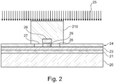
- Fig. 2 shows a silicon on insulator substrate which includes a supporting silicon substrate 20, a buried oxide layer 23 and an active silicon layer 24.
- the supporting silicon substrate 20 may have a comparatively high resistance (corresponding to a low dopant concentration) of 300 Qcm to 1 k ⁇ cm or more, but is not restricted thereto.
- a trap-rich layer 21 is provided which serves to trap free charge carriers at interfaces, for example at the interface between oxide 23 and trap-rich layer 21 or at the interface between trap-rich layer 21 and supporting silicon substrate 20.
- Active layer 24 is the layer at, i.e. in and/or on, which devices like a radio frequency device are formed.
- a field effect transistor is formed as a radio frequency device.
- a source region 27 and a drain region 26 are formed in active layer 24 separated by a body region 29.
- source and drain regions 27, 26 may be formed by doping for example using ion implantation (n-type doping for an n-type transistor and p-type doping for a p-type transistor), while body region 29 has a low dopant concentration.
- source and drain regions 27, 26 may be n-type doped using phosphorous or arsenic, while body region may be weakly p-doped.
- a polysilicon gate, 28 is formed above body region 29 separated from active layer 24, in particular body region 29, by a gate dielectric like a silicon oxide layer.
- a metal gate may be formed.
- a plurality of such transistors may be formed and coupled in series to provide a radio frequency switch.
- the transistor shown in Fig. 2 is merely an example for a radio frequency device, and other devices, both active and passive may be formed as well in any conventional manner.
- the method of Fig. 1 comprises an ion implantation around the frequency device.
- An ion implantation may create a defect rich region. Defects in the defect rich region may trap free charge carriers, which in some cases may help to improve linearity. For example, by ion implantation defects are formed which provide recombination centers reducing lifetime of charge carriers like minority carriers, thus reducing the number of free charge carriers. Energy levels of such recombination centers may be at or near an intrinsic Fermi level. For example, Argon may form a deep level at 0.5 eV.
- a defect rich region is to be understood as a region where sufficient defects are formed to reduce the density of free charge carriers.
- a photoresist layer 210 is formed above the radio frequency transistor. Then an ion implantation, for example an argon ion implantation, is performed as indicated by arrows 25.
- an ion implantation for example an argon ion implantation, is performed as indicated by arrows 25.
- a region of the radio frequency transistor (or other radio frequency device in other implementations) is protected against the ion implantation, whereas a region around the radio frequency transistor is implanted with ions like argon ions, to form a defect rich region.
- Typical Argon doses may be in the range of 5x10 14 /cm 2 to 2x10 15 /cm 2 with an energy between 120keV and 500keV, but are not limited thereto. Furthermore, doses may depend on the type of ions used.
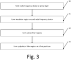
- Fig. 3 illustrates a method according to a further embodiment.
- the method of Fig. 3 will be explained jointly with a device illustrated in Figs. 4A and 4B , where Fig. 4A shows a cross-sectional view and Fig. 4B shows a top view of a device according to an embodiment.
- Fig. 4A shows a cross-sectional view
- Fig. 4B shows a top view of a device according to an embodiment.
- Features corresponding to features already explained with reference to Fig. 2 bear the same reference numeral in Figs. 4A and 4B and will not be described again in detail.
- the method illustrated in Fig. 3 comprises forming a radio frequency device at an active layer of a silicon on insulator substrate.
- This forming of a radio frequency device at 30 may correspond to the forming of a radio frequency device at 10 in Fig. 1 , and the variations and possibilities for forming such a device explained with reference to Figs. 1 and 2 also apply to the forming at 30 in Fig. 3 .
- a silicon on insulator substrate comprising a supporting silicon substrate 20, a trap-rich layer 21, a buried oxide layer 23 and an active layer 24 is used.
- a radio frequency device as in Fig. 2 a radio frequency transistor having a source region 27, a drain region 26 and a polysilicon gate 28 above a body region 29 is used.
- Polysilicon gate 28 is part of a polysilicon layer 40 above active layer 24.
- an insulation region is formed around the radio frequency device, in particular in the active layer.
- a shallow trench insulation (STI) region 41 is formed around the radio frequency device.
- silicon filler regions are formed in the insulation region.
- silicon filler regions 42 are formed. These regions may be randomly distributed within the insulation region, as indicated by an irregular distribution as seen in the top view of Fig. 4B .
- such filler regions are used in semiconductor device manufacturing to facilitate manufacturing of the device.
- the forming of the silicon filler regions may be effected by forming the insulation region in the active layer 24 apart from the silicon filler regions, such that the silicon filler regions are formed by remaining silicon of the original active layer of the silicon on insulator substrate.
- the forming of the silicon filler regions may also happen implicitly in the processing, by leaving certain regions of silicon unprocessed when forming the insulation region.
- Such an implicit forming is also to be regarded as "forming silicon filler regions" in the context of the present specification.
- Typical sizes of such silicon filler regions may be of the order of about 0.4x0.4 ⁇ m 2 , but larger or smaller structures or non-square structures may also be used. For example, sizes of up to 5x5 ⁇ m 2 may be used.
- a density of the filler regions may be such that they cover about 4% of the area, but other values are also possible, for example up to 55%.
- the silicon filler regions may be undoped to reduce free charge carriers. "Undoped” in this case means that no intentional doping is performed. It is understood by the skilled person that some amount of impurities may nevertheless be present unintentionally which may cause some doping.
- the method comprises forming polysilicon filler regions at offset positions to the silicon filler regions above the active layer, in particular in a polysilicon layer.
- Fig. 4A as an example polysilicon filler regions 43 are shown. Offset positions means that the polysilicon filler regions, in a top view of the substrate (for example top view of Fig. 4B ) are formed at different positions compared to the silicon filler regions.
- the polysilicon filler regions 43 are formed without overlap with the silicon filler regions in the top view of Fig. 4B .
- no polysilicon filler regions are formed above the silicon filler regions, as shown for crossed-out polysilicon filler region 44 in Fig. 4A .
- a direction parallel to the surface of the substrate is taken as lateral direction, as often used in semiconductor technology, it can also be said that the polysilicon filler regions are formed laterally offset or at laterally different positions, in particular without lateral overlap to the silicon filler regions.
- Forming of the polysilicon filler regions also may facilitate processing of the devices. It should be noted that the polysilicon filler regions may be formed in the same process as the polysilicon gate 28. This is an example where parts of various acts or events of the method of Fig. 3 , in this case a part of forming the radio frequency device, and the forming of the polysilicon filler regions, are performed simultaneously.
- Using the laterally offset positions may prevent or reduce the forming of free charge carriers which could otherwise be formed at interfaces between polysilicon filler regions and silicon filler regions. This, in turn, in some embodiments may help to increase linearity.
- Figs. 1 and 3 may be combined, by performing both the ion implantation at 11 in Fig. 1 and forming the insulation region, silicon filler regions and polysilicon filler regions at 31 to 33 of Fig. 3 .
- the ion implantation may be performed after forming the silicon filler regions and the polysilicon filler regions, such that these regions are also subjected to ion implantation like argon ion implantation.
- a corresponding device in a particular stage of processing is illustrated in Fig. 5.
- Fig. 5 is essentially a combination of Figs. 2 and 4A , and corresponding elements bear the same reference numerals.
- the shallow trench insulation region 41 with the silicon filler regions 42 is formed in active layer 24, and polysilicon filler regions 43 are formed at laterally offset positions to the silicon filler regions 42 in a polysilicon layer 40.
- the radio frequency transistor is protected by a photoresist 210 against ion implantation as indicated by arrows 25, such that at least a part of insulation region 41 outside photoresist 210 as well as polysilicon filler regions 43 and silicon filler regions 42 are ion implanted to form defect rich regions.
- the combination of these measures may further reduce free-charge carriers, leading to an increase of linearity in some implementations.
Landscapes
- Semiconductor Integrated Circuits (AREA)
- Thin Film Transistor (AREA)
- Element Separation (AREA)
Abstract
Description
- The present application relates to devices including radio frequency (RF) devices and methods related thereto, in particular methods for manufacturing such devices.
- Radio frequency devices are for example used in communication circuits. Examples for radio frequency devices are transistor-based radio frequency switches, which in some implementations may be formed by coupling a plurality of transistors in series. Other examples may include passive radio frequency devices. Radio frequency, as used herein, may relate to frequencies above 100 kHz, in particular in the MHz range or GHz range. For example, for the upcoming 5G (5th generation) mobile communication standard frequencies up to 300 GHz will be used. In some cases, to improve performance, radio frequency devices are manufactured on silicon on insulator (SOI) substrates.
- For such radio frequency devices, specification requirements are becoming more and more strict. For example, an improved linearity of the devices may be required.
- According to some embodiment, methods and devices as defined in the independent claims are provided. The dependent claims defined further embodiments.
- According to an embodiment, a method is provided, comprising:
- forming a radio frequency device at an active layer of a silicon on insulator substrate, and
- ion implanting a region around the radio frequency device to form a defect rich region to reduce a free charge carrier density.
- According to another embodiment, a method is provided, comprising:
- forming a radio frequency device at an active layer of a silicon on insulator substrate,
- forming an insulation region in a region around the radio frequency device,
- forming silicon filler regions in the insulation region, and forming polysilicon filler regions above the insulation region, wherein the polysilicon filler regions are provided at different positions than the silicon filler regions in a top view on the substrate.
- According to another embodiment, a device is provided, comprising:
- a silicon on insulator substrate,
- a radio frequency device at an active layer of the silicon on insulator substrate, and
- a defect rich region around the radio frequency device.
- According to a further embodiment, a device is provided, comprising:
- a silicon on insulator substrate,
- a radio frequency device at an active layer of the silicon on insulator substrate,
- in the active layer, an insulation region around the radio frequency device,
- silicon filler regions in the insulation region, and polysilicon filler regions above the insulation region, wherein the polysilicon filler regions are provided at different positions than the silicon filler regions in a top view on the substrate.
- The above summary is merely intended to give a brief overview over some embodiments and is not to be construed as limiting in any way, as other embodiments may comprise other features than the ones explicitly mentioned above.
-
-
Fig. 1 is a flow chart illustrating a method according to an embodiment. -
Fig. 2 is a cross-sectional view illustrating a device according to an embodiment. -
Fig. 3 is a flow chart illustrating a method according to an embodiment. -
Fig. 4A is a cross-sectional view illustrating a device according to an embodiment. -
Fig. 4B is a top view of the device ofFig. 4A . -
Fig. 5 is a cross-sectional view illustrating a device according to a further embodiment. - In the following, various embodiments will be described in detail referring to the attached drawings.
- It is to be understood that these embodiments are given for illustrative purposes and are not to be construed as limiting in any way. For example, while embodiments may be described as comprising a plurality of features, elements, process steps and the like, in other embodiments, some of these features, elements or process steps may be omitted or replaced by alternative features, elements or process steps.
- In addition to the features, elements or process steps explicitly shown and described, other features, elements or process steps may be provided, for example features, elements or process steps used in conventional radio frequency devices and manufacturing thereof.
- Embodiments use silicon on insulator wafers and substrates. Silicon on insulator wafers and substrates are layered wafers and substrates which may be used for example to reduce parasitic capacitances within devices, for example radio frequency devices. Silicon on insulator wafers generally comprise at least a supporting silicon substrate, an active silicon layer and an oxide layer between the active silicon layer and the supporting silicon substrate. The active silicon layer denotes the silicon layer at which devices are formed. "At" the active silicon layer in this case means in the active silicon layer, for example by modifying portions of the active silicon layer by techniques like ion implantation, etching and the like, and/or on top of the active silicon layer, for example by depositing or structuring additional layers on the active silicon layer. In some silicon on insulator wafers, additional layers may be present, for example a trap-rich layer, like a polysilicon layer between the oxide layer and the supporting silicon substrate. Various techniques are used to manufacture silicon on insulator substrate, like wafer bonding techniques or oxygen implantation techniques. As such silicon on insulator substrates and wafers or commercially available, they will not be further described here.
-
Fig. 1 is a flow chart illustrating a method for manufacturing a device according to some embodiments. For better understanding, the method ofFig. 1 will be described also referring toFig. 2 , which shows a cross-sectional view of a device at a particular stage of processing in an example implementation of a method as shown inFig. 1 . It should nevertheless be noted that the method ofFig. 1 and the device ofFig. 2 may also be implemented independently from each other, and the joint description merely serves to provide a better understanding. - The method shown in
Fig. 1 , at 10, comprises forming a radio frequency device at an active layer of a silicon on insulator substrate. As an example,Fig. 2 shows a silicon on insulator substrate which includes a supportingsilicon substrate 20, a buriedoxide layer 23 and anactive silicon layer 24. The supportingsilicon substrate 20 may have a comparatively high resistance (corresponding to a low dopant concentration) of 300 Qcm to 1 kΩcm or more, but is not restricted thereto. - In the example of
Fig. 2 , between buriedoxide layer 23 and supportingsilicon substrate 20, a trap-rich layer 21 is provided which serves to trap free charge carriers at interfaces, for example at the interface betweenoxide 23 and trap-rich layer 21 or at the interface between trap-rich layer 21 and supportingsilicon substrate 20. -
Active layer 24 is the layer at, i.e. in and/or on, which devices like a radio frequency device are formed. As an example, inFig. 2 a field effect transistor is formed as a radio frequency device. To form the transistor, asource region 27 and adrain region 26 are formed inactive layer 24 separated by abody region 29. In some implementations, source anddrain regions body region 29 has a low dopant concentration. For example, for forming an n-type field effect transistor, source and drainregions - Furthermore, a polysilicon gate, 28, is formed above
body region 29 separated fromactive layer 24, inparticular body region 29, by a gate dielectric like a silicon oxide layer. - In other implementations, a metal gate may be formed. In some implementations, a plurality of such transistors may be formed and coupled in series to provide a radio frequency switch. The transistor shown in
Fig. 2 is merely an example for a radio frequency device, and other devices, both active and passive may be formed as well in any conventional manner. - At 11, the method of
Fig. 1 comprises an ion implantation around the frequency device. An ion implantation may create a defect rich region. Defects in the defect rich region may trap free charge carriers, which in some cases may help to improve linearity. For example, by ion implantation defects are formed which provide recombination centers reducing lifetime of charge carriers like minority carriers, thus reducing the number of free charge carriers. Energy levels of such recombination centers may be at or near an intrinsic Fermi level. For example, Argon may form a deep level at 0.5 eV. A defect rich region is to be understood as a region where sufficient defects are formed to reduce the density of free charge carriers. - In the example of
Fig. 2 , for performing the ion implantation aphotoresist layer 210 is formed above the radio frequency transistor. Then an ion implantation, for example an argon ion implantation, is performed as indicated byarrows 25. By thephotoresist 210, a region of the radio frequency transistor (or other radio frequency device in other implementations) is protected against the ion implantation, whereas a region around the radio frequency transistor is implanted with ions like argon ions, to form a defect rich region. Typical Argon doses may be in the range of 5x10¹⁴/cm2 to 2x10¹⁵/cm2 with an energy between 120keV and 500keV, but are not limited thereto. Furthermore, doses may depend on the type of ions used. -
Fig. 3 illustrates a method according to a further embodiment. The method ofFig. 3 will be explained jointly with a device illustrated inFigs. 4A and4B , whereFig. 4A shows a cross-sectional view andFig. 4B shows a top view of a device according to an embodiment. Features corresponding to features already explained with reference toFig. 2 bear the same reference numeral inFigs. 4A and4B and will not be described again in detail. - It should be noted that the various acts and events described with reference to
Fig. 3 are not necessarily performed in the order shown and described, but depending on processing technologies, other orders may be used or certain parts of the various acts and events may be performed simultaneously. Examples for this will be given in the course of the description ofFig. 3 . - At 30, the method illustrated in
Fig. 3 comprises forming a radio frequency device at an active layer of a silicon on insulator substrate. This forming of a radio frequency device at 30 may correspond to the forming of a radio frequency device at 10 inFig. 1 , and the variations and possibilities for forming such a device explained with reference toFigs. 1 and2 also apply to the forming at 30 inFig. 3 . - In the example device of
Figs. 4A and4B , as inFig. 2 a silicon on insulator substrate comprising a supportingsilicon substrate 20, a trap-rich layer 21, a buriedoxide layer 23 and anactive layer 24 is used. As an example for a radio frequency device, as inFig. 2 a radio frequency transistor having asource region 27, adrain region 26 and apolysilicon gate 28 above abody region 29 is used.Polysilicon gate 28 is part of apolysilicon layer 40 aboveactive layer 24. - At 31 in
Fig. 3 , an insulation region is formed around the radio frequency device, in particular in the active layer. As an example, inFigs. 4A and4B a shallow trench insulation (STI)region 41 is formed around the radio frequency device. - At 32, silicon filler regions are formed in the insulation region. For example, in
Fig. 4A silicon filler regions 42 are formed. These regions may be randomly distributed within the insulation region, as indicated by an irregular distribution as seen in the top view ofFig. 4B . Generally, such filler regions are used in semiconductor device manufacturing to facilitate manufacturing of the device. It should be noted that the forming of the silicon filler regions may be effected by forming the insulation region in theactive layer 24 apart from the silicon filler regions, such that the silicon filler regions are formed by remaining silicon of the original active layer of the silicon on insulator substrate. In other words, the forming of the silicon filler regions may also happen implicitly in the processing, by leaving certain regions of silicon unprocessed when forming the insulation region. Such an implicit forming is also to be regarded as "forming silicon filler regions" in the context of the present specification. - Typical sizes of such silicon filler regions may be of the order of about 0.4x0.4 µm2, but larger or smaller structures or non-square structures may also be used. For example, sizes of up to 5x5µm2 may be used. A density of the filler regions may be such that they cover about 4% of the area, but other values are also possible, for example up to 55%.
- In some embodiments, the silicon filler regions may be undoped to reduce free charge carriers. "Undoped" in this case means that no intentional doping is performed. It is understood by the skilled person that some amount of impurities may nevertheless be present unintentionally which may cause some doping.
- At 33, the method comprises forming polysilicon filler regions at offset positions to the silicon filler regions above the active layer, in particular in a polysilicon layer.
- In
Fig. 4A , as an examplepolysilicon filler regions 43 are shown. Offset positions means that the polysilicon filler regions, in a top view of the substrate (for example top view ofFig. 4B ) are formed at different positions compared to the silicon filler regions. In the embodiment ofFigs. 4A and4B , in particular thepolysilicon filler regions 43 are formed without overlap with the silicon filler regions in the top view ofFig. 4B . In other words, no polysilicon filler regions are formed above the silicon filler regions, as shown for crossed-outpolysilicon filler region 44 inFig. 4A . - If a direction parallel to the surface of the substrate is taken as lateral direction, as often used in semiconductor technology, it can also be said that the polysilicon filler regions are formed laterally offset or at laterally different positions, in particular without lateral overlap to the silicon filler regions.
- Forming of the polysilicon filler regions also may facilitate processing of the devices. It should be noted that the polysilicon filler regions may be formed in the same process as the
polysilicon gate 28. This is an example where parts of various acts or events of the method ofFig. 3 , in this case a part of forming the radio frequency device, and the forming of the polysilicon filler regions, are performed simultaneously. - Using the laterally offset positions may prevent or reduce the forming of free charge carriers which could otherwise be formed at interfaces between polysilicon filler regions and silicon filler regions. This, in turn, in some embodiments may help to increase linearity.
- It should be noted that the methods of
Figs. 1 and3 may be combined, by performing both the ion implantation at 11 inFig. 1 and forming the insulation region, silicon filler regions and polysilicon filler regions at 31 to 33 ofFig. 3 . - The ion implantation may be performed after forming the silicon filler regions and the polysilicon filler regions, such that these regions are also subjected to ion implantation like argon ion implantation. A corresponding device in a particular stage of processing is illustrated in
Fig. 5. Fig. 5 is essentially a combination ofFigs. 2 and4A , and corresponding elements bear the same reference numerals. In particular, inFig. 5 around the radio frequency transistor the shallowtrench insulation region 41 with thesilicon filler regions 42 is formed inactive layer 24, andpolysilicon filler regions 43 are formed at laterally offset positions to thesilicon filler regions 42 in apolysilicon layer 40. The radio frequency transistor is protected by aphotoresist 210 against ion implantation as indicated byarrows 25, such that at least a part ofinsulation region 41 outsidephotoresist 210 as well aspolysilicon filler regions 43 andsilicon filler regions 42 are ion implanted to form defect rich regions. The combination of these measures may further reduce free-charge carriers, leading to an increase of linearity in some implementations. - Some embodiments are defined by the following examples:
- Example 1. A method, comprising:
- forming a radio frequency device at an active layer of a silicon on insulator substrate, and
- ion implanting a region around the radio frequency device to form a defect rich region to reduce a free charge carrier density.
- Example 2. The method of example 1, wherein ion implanting comprises implanting with Argon ions.
- Example 3. The method of example 1 or 2, further comprising forming, in the active layer, an insulation region in the region around the radio frequency device prior to the ion implanting.
- Example 4. The method of example 3, further comprising forming silicon filler regions in the insulation region and polysilicon filler regions above the insulation region, wherein the polysilicon filler regions are provided at different positions than the silicon filler regions in a top view on the substrate.
- Example 5. The method of example 4, wherein the silicon filler regions and/or the polysilicon filler regions are undoped.
- Example 6. A method, comprising:
- forming a radio frequency device at an active layer of a silicon on insulator substrate,
- forming an insulation region in a region around the radio frequency device,
- forming silicon filler regions in the insulation region, and forming polysilicon filler regions above the insulation region, wherein the polysilicon filler regions are provided at different positions than the silicon filler regions in a top view on the substrate.
- Example 7. The method of example 6, wherein the silicon filler regions and/or the polysilicon filler regions are undoped.
- Example 8. The method of example 6 or 7, further comprising ion implanting in at least some of the silicon filler regions and/or the polysilicon filler regions to form defect rich regions to reduce a free charge carrier density.
- Example 9. The method of example 8, wherein ion implanting comprises implanting with Argon ions.
- Example 10. The method of example 6, wherein the polysilicon filler regions are provided without overlap with the silicon filler regions in a top view on the substrate.
- Example 11. A device, comprising:
- a silicon on insulator substrate,
- a radio frequency device at an active layer of the silicon on insulator substrate, and
- a defect rich region around the radio frequency device.
- Example 12. The device of example 11, wherein the defect rich region comprises an ion implanted region.
- Example 13. The device of example 11 or 12, further comprising, in the active layer, an insulation region at least partially overlapping with the defect rich region.
- Example 14. The device of example 13, further comprising silicon filler regions in the insulation region and polysilicon filler regions above the insulation region, wherein the polysilicon filler regions are provided at different positions than the silicon filler regions in a top view on the substrate.
- Example 15. The device of example 14, wherein the silicon filler regions and/or the polysilicon filler regions are undoped.
- Example 16. A device, comprising:
- a silicon on insulator substrate,
- a radio frequency device at an active layer of the silicon on insulator substrate,
- in the active layer, an insulation region around the radio frequency device,
- silicon filler regions in the insulation region, and polysilicon filler regions above the insulation region, wherein the polysilicon filler regions are provided at different positions than the silicon filler regions in a top view on the substrate.
- Example 17. The device of example 16, wherein the silicon filler regions and/or the polysilicon filler regions are undoped.
- Example 18. The device of example 16 or 17, wherein at least some of the silicon filler regions and/or the polysilicon filler regions are ion implanted.
- Example 19. The device of example 18, where the at least some of the silicon filler regions and/or the polysilicon filler regions are Argon ion implanted.
- Example 20. The device of any one of examples 16 to 19, wherein the polysilicon filler regions are provided without overlap with the silicon filler regions in a top view on the substrate.
- Although specific embodiments have been illustrated and described herein, it will be appreciated by those of ordinary skill in the art that a variety of alternate and/or equivalent implementations may be substituted for the specific embodiments shown and described without departing from the scope of the present invention. This application is intended to cover any adaptations or variations of the specific embodiments discussed herein. Therefore, it is intended that this invention be limited only by the claims and the equivalents thereof.
Claims (15)
- A method, comprising:forming a radio frequency device (26, 27, 28, 29) at an active layer (24) of a silicon on insulator substrate (20, 21, 22, 23) andion implanting (25) a region around the radio frequency device (26, 27, 28, 29) to form a defect rich region to reduce a free charge carrier density.
- The method of claim 1, wherein ion implanting (25) comprises implanting with Argon ions.
- The method of claim 1 or 2, further comprising forming, in the active layer (24), an insulation region (41) in the region around the radio frequency device (26, 27, 28, 29) prior to the ion implanting (25).
- The method of claim 3, further comprising forming silicon filler regions (42) in the insulation region (41) and polysilicon filler regions (43) above the insulation region (41), wherein the polysilicon filler regions (43) are provided at different positions than the silicon filler regions (42) in a top view on the substrate.
- The method of claim 4, wherein the silicon filler regions (42) and/or the polysilicon filler regions (43) are undoped.
- A method, comprising:forming a radio frequency device (26, 27, 28, 29) at an active layer (24) of a silicon on insulator substrate (20, 21, 22, 23),forming an insulation region (41) in a region around the radio frequency device(26, 27, 28, 29),forming silicon filler regions (42) in the insulation region (41), andforming polysilicon filler regions (43) above the insulation region (41), wherein the polysilicon filler regions (43) are provided at different positions than the silicon filler regions (42) in a top view on the substrate.
- The method of claim 6, wherein the silicon filler regions (42) and/or the polysilicon filler regions (43) are undoped.
- The method of claim 6 or 7, further comprising ion implanting (25) in at least some of the silicon filler regions (42) and/or the polysilicon filler regions (43) to form defect rich regions to reduce a free charge carrier density.
- A device, comprising:a silicon on insulator substrate (20, 21, 22, 23),a radio frequency device (26, 27, 28, 29) at an active layer (24) of the silicon on insulator substrate (20, 21, 22, 23), anda defect rich region around the radio frequency device (26, 27, 28, 29).
- The device of claim 9, wherein the defect rich region comprises an ion implanted region.
- The device of claim 9 or 10, further comprising, in the active layer (24), an insulation region (41) at least partially overlapping with the defect rich region.
- The device of claim 11, further comprising silicon filler regions (42) in the insulation region (41) and polysilicon filler regions (43) above the insulation region (41), wherein the polysilicon filler regions (43) are provided at different positions than the silicon filler regions (42) in a top view on the substrate.
- The device of claim 12, wherein the silicon filler regions (42) and/or the polysilicon filler regions (43) are undoped.
- A device, comprising:a silicon on insulator substrate (20, 21, 22, 23),a radio frequency device (26, 27, 28, 29) at an active layer (24) of the silicon on insulator substrate (20, 21, 22, 23), in the active layer (24), an insulation region (41) around the radio frequency device (26, 27, 28, 29),silicon filler regions (42) in the insulation region (41), andpolysilicon filler regions (43) above the insulation region (41), wherein the polysilicon filler regions (43) are provided at different positions than the silicon filler regions (42) in a top view on the substrate.
- The device of claim 14, wherein the silicon filler regions (42) and/or the polysilicon filler regions (43) are undoped.
Priority Applications (1)
| Application Number | Priority Date | Filing Date | Title |
|---|---|---|---|
| EP19209444.9A EP3823014B1 (en) | 2019-11-15 | 2019-11-15 | Devices including radio frequency devices and methods |
Applications Claiming Priority (1)
| Application Number | Priority Date | Filing Date | Title |
|---|---|---|---|
| EP19209444.9A EP3823014B1 (en) | 2019-11-15 | 2019-11-15 | Devices including radio frequency devices and methods |
Publications (3)
| Publication Number | Publication Date |
|---|---|
| EP3823014A2 true EP3823014A2 (en) | 2021-05-19 |
| EP3823014A3 EP3823014A3 (en) | 2021-06-09 |
| EP3823014B1 EP3823014B1 (en) | 2024-07-31 |
Family
ID=68609886
Family Applications (1)
| Application Number | Title | Priority Date | Filing Date |
|---|---|---|---|
| EP19209444.9A Active EP3823014B1 (en) | 2019-11-15 | 2019-11-15 | Devices including radio frequency devices and methods |
Country Status (1)
| Country | Link |
|---|---|
| EP (1) | EP3823014B1 (en) |
Cited By (1)
| Publication number | Priority date | Publication date | Assignee | Title |
|---|---|---|---|---|
| US20230369337A1 (en) * | 2022-05-16 | 2023-11-16 | Skyworks Solutions, Inc. | Noise reduction in silicon-on-insulator devices |
Family Cites Families (4)
| Publication number | Priority date | Publication date | Assignee | Title |
|---|---|---|---|---|
| KR0154292B1 (en) * | 1995-06-20 | 1998-12-01 | 김주용 | Method of element isolating film for semiconductor device |
| US7875931B2 (en) * | 2006-04-28 | 2011-01-25 | Semiconductor Energy Laboratory Co., Ltd. | Semiconductor device with isolation using impurity |
| US20080217727A1 (en) * | 2007-03-11 | 2008-09-11 | Skyworks Solutions, Inc. | Radio frequency isolation for SOI transistors |
| US20150228714A1 (en) * | 2014-02-13 | 2015-08-13 | Rfaxis, Inc. | Isolation methods for leakage, loss and non-linearity mitigation in radio-frequency integrated circuits on high-resistivity silicon-on-insulator substrates |
-
2019
- 2019-11-15 EP EP19209444.9A patent/EP3823014B1/en active Active
Cited By (3)
| Publication number | Priority date | Publication date | Assignee | Title |
|---|---|---|---|---|
| US20230369337A1 (en) * | 2022-05-16 | 2023-11-16 | Skyworks Solutions, Inc. | Noise reduction in silicon-on-insulator devices |
| US12593511B2 (en) | 2022-05-16 | 2026-03-31 | Skyworks Solutions, Inc. | Radio frequency interference mitigation for silicon-on-insulator devices |
| US12598812B2 (en) * | 2022-05-16 | 2026-04-07 | Skyworks Solutions, Inc. | Noise reduction in silicon-on-insulator devices |
Also Published As
| Publication number | Publication date |
|---|---|
| EP3823014A3 (en) | 2021-06-09 |
| EP3823014B1 (en) | 2024-07-31 |
Similar Documents
| Publication | Publication Date | Title |
|---|---|---|
| US6717211B2 (en) | Shallow doped junctions with a variable profile gradation of dopants | |
| CN101897017B (en) | Semiconductor device and method for manufacturing semiconductor device | |
| US10381259B2 (en) | Semiconductor device with localized carrier lifetime reduction and fabrication method thereof | |
| US6828635B2 (en) | Method for making high-gain vertical bipolar junction transistor structures compatible with CMOS process | |
| US8212292B2 (en) | High gain tunable bipolar transistor | |
| US20120267724A1 (en) | Mos semiconductor device and methods for its fabrication | |
| JP2011119344A (en) | Semiconductor apparatus, and method for manufacturing the same | |
| JP5687844B2 (en) | Hybrid semiconductor substrate manufacturing process | |
| US20120261804A1 (en) | Vertical substrate diode, method of manufacture and design structure | |
| US20060011981A1 (en) | High frequency MOS transistor, method of forming the same, and method of manufacturing a semiconductor device including the same | |
| US10217828B1 (en) | Transistors with field plates on fully depleted silicon-on-insulator platform and method of making the same | |
| US20130134550A1 (en) | Semiconductor device and method of manufacturing the same | |
| JP2002043567A (en) | Semiconductor device and method of manufacturing the same | |
| US10910493B2 (en) | Semiconductor device and method of manufacturing the same | |
| US8841723B2 (en) | LDMOS device having increased punch-through voltage and method for making same | |
| US6566680B1 (en) | Semiconductor-on-insulator (SOI) tunneling junction transistor | |
| EP3823014B1 (en) | Devices including radio frequency devices and methods | |
| US20050093032A1 (en) | Transistor having a germanium implant region located therein and a method of manufacture therefor | |
| US7863144B2 (en) | Semiconductor device and method for manufacturing the device | |
| US20130099288A1 (en) | SiGe HBT and Manufacturing Method Thereof | |
| US6774455B2 (en) | Semiconductor device with a collector contact in a depressed well-region | |
| US20060284278A1 (en) | Area diode formation in SOI application | |
| KR20040038379A (en) | Smart power device built-in SiGe HBT and fabrication method of the same | |
| CN119815905B (en) | Radio frequency low noise MOSFET transistor with buried layer structure and manufacturing method | |
| CN118969819B (en) | Semiconductor structure, manufacturing method of semiconductor structure and NMOS transistor |
Legal Events
| Date | Code | Title | Description |
|---|---|---|---|
| PUAI | Public reference made under article 153(3) epc to a published international application that has entered the european phase |
Free format text: ORIGINAL CODE: 0009012 |
|
| STAA | Information on the status of an ep patent application or granted ep patent |
Free format text: STATUS: THE APPLICATION HAS BEEN PUBLISHED |
|
| PUAL | Search report despatched |
Free format text: ORIGINAL CODE: 0009013 |
|
| AK | Designated contracting states |
Kind code of ref document: A2 Designated state(s): AL AT BE BG CH CY CZ DE DK EE ES FI FR GB GR HR HU IE IS IT LI LT LU LV MC MK MT NL NO PL PT RO RS SE SI SK SM TR |
|
| AK | Designated contracting states |
Kind code of ref document: A3 Designated state(s): AL AT BE BG CH CY CZ DE DK EE ES FI FR GB GR HR HU IE IS IT LI LT LU LV MC MK MT NL NO PL PT RO RS SE SI SK SM TR |
|
| RIC1 | Information provided on ipc code assigned before grant |
Ipc: H01L 21/762 20060101AFI20210503BHEP Ipc: H01L 21/76 20060101ALI20210503BHEP Ipc: H01L 21/84 20060101ALI20210503BHEP Ipc: H01L 27/12 20060101ALI20210503BHEP Ipc: H01L 21/322 20060101ALI20210503BHEP |
|
| STAA | Information on the status of an ep patent application or granted ep patent |
Free format text: STATUS: REQUEST FOR EXAMINATION WAS MADE |
|
| 17P | Request for examination filed |
Effective date: 20211207 |
|
| RBV | Designated contracting states (corrected) |
Designated state(s): AL AT BE BG CH CY CZ DE DK EE ES FI FR GB GR HR HU IE IS IT LI LT LU LV MC MK MT NL NO PL PT RO RS SE SI SK SM TR |
|
| GRAP | Despatch of communication of intention to grant a patent |
Free format text: ORIGINAL CODE: EPIDOSNIGR1 |
|
| STAA | Information on the status of an ep patent application or granted ep patent |
Free format text: STATUS: GRANT OF PATENT IS INTENDED |
|
| INTG | Intention to grant announced |
Effective date: 20240222 |
|
| GRAS | Grant fee paid |
Free format text: ORIGINAL CODE: EPIDOSNIGR3 |
|
| GRAA | (expected) grant |
Free format text: ORIGINAL CODE: 0009210 |
|
| STAA | Information on the status of an ep patent application or granted ep patent |
Free format text: STATUS: THE PATENT HAS BEEN GRANTED |
|
| AK | Designated contracting states |
Kind code of ref document: B1 Designated state(s): AL AT BE BG CH CY CZ DE DK EE ES FI FR GB GR HR HU IE IS IT LI LT LU LV MC MK MT NL NO PL PT RO RS SE SI SK SM TR |
|
| REG | Reference to a national code |
Ref country code: CH Ref legal event code: EP Ref country code: GB Ref legal event code: FG4D |
|
| P01 | Opt-out of the competence of the unified patent court (upc) registered |
Free format text: CASE NUMBER: APP_42002/2024 Effective date: 20240716 |
|
| REG | Reference to a national code |
Ref country code: DE Ref legal event code: R096 Ref document number: 602019056037 Country of ref document: DE |
|
| REG | Reference to a national code |
Ref country code: IE Ref legal event code: FG4D |
|
| REG | Reference to a national code |
Ref country code: LT Ref legal event code: MG9D |
|
| REG | Reference to a national code |
Ref country code: NL Ref legal event code: MP Effective date: 20240731 |
|
| PG25 | Lapsed in a contracting state [announced via postgrant information from national office to epo] |
Ref country code: PT Free format text: LAPSE BECAUSE OF FAILURE TO SUBMIT A TRANSLATION OF THE DESCRIPTION OR TO PAY THE FEE WITHIN THE PRESCRIBED TIME-LIMIT Effective date: 20241202 |
|
| REG | Reference to a national code |
Ref country code: AT Ref legal event code: MK05 Ref document number: 1709310 Country of ref document: AT Kind code of ref document: T Effective date: 20240731 |
|
| PG25 | Lapsed in a contracting state [announced via postgrant information from national office to epo] |
Ref country code: PT Free format text: LAPSE BECAUSE OF FAILURE TO SUBMIT A TRANSLATION OF THE DESCRIPTION OR TO PAY THE FEE WITHIN THE PRESCRIBED TIME-LIMIT Effective date: 20241202 |
|
| PG25 | Lapsed in a contracting state [announced via postgrant information from national office to epo] |
Ref country code: NO Free format text: LAPSE BECAUSE OF FAILURE TO SUBMIT A TRANSLATION OF THE DESCRIPTION OR TO PAY THE FEE WITHIN THE PRESCRIBED TIME-LIMIT Effective date: 20241031 |
|
| PG25 | Lapsed in a contracting state [announced via postgrant information from national office to epo] |
Ref country code: FI Free format text: LAPSE BECAUSE OF FAILURE TO SUBMIT A TRANSLATION OF THE DESCRIPTION OR TO PAY THE FEE WITHIN THE PRESCRIBED TIME-LIMIT Effective date: 20240731 Ref country code: NL Free format text: LAPSE BECAUSE OF FAILURE TO SUBMIT A TRANSLATION OF THE DESCRIPTION OR TO PAY THE FEE WITHIN THE PRESCRIBED TIME-LIMIT Effective date: 20240731 Ref country code: GR Free format text: LAPSE BECAUSE OF FAILURE TO SUBMIT A TRANSLATION OF THE DESCRIPTION OR TO PAY THE FEE WITHIN THE PRESCRIBED TIME-LIMIT Effective date: 20241101 Ref country code: PL Free format text: LAPSE BECAUSE OF FAILURE TO SUBMIT A TRANSLATION OF THE DESCRIPTION OR TO PAY THE FEE WITHIN THE PRESCRIBED TIME-LIMIT Effective date: 20240731 |
|
| PG25 | Lapsed in a contracting state [announced via postgrant information from national office to epo] |
Ref country code: BG Free format text: LAPSE BECAUSE OF FAILURE TO SUBMIT A TRANSLATION OF THE DESCRIPTION OR TO PAY THE FEE WITHIN THE PRESCRIBED TIME-LIMIT Effective date: 20240731 |
|
| PG25 | Lapsed in a contracting state [announced via postgrant information from national office to epo] |
Ref country code: LV Free format text: LAPSE BECAUSE OF FAILURE TO SUBMIT A TRANSLATION OF THE DESCRIPTION OR TO PAY THE FEE WITHIN THE PRESCRIBED TIME-LIMIT Effective date: 20240731 |
|
| PG25 | Lapsed in a contracting state [announced via postgrant information from national office to epo] |
Ref country code: AT Free format text: LAPSE BECAUSE OF FAILURE TO SUBMIT A TRANSLATION OF THE DESCRIPTION OR TO PAY THE FEE WITHIN THE PRESCRIBED TIME-LIMIT Effective date: 20240731 Ref country code: IS Free format text: LAPSE BECAUSE OF FAILURE TO SUBMIT A TRANSLATION OF THE DESCRIPTION OR TO PAY THE FEE WITHIN THE PRESCRIBED TIME-LIMIT Effective date: 20241130 |
|
| PG25 | Lapsed in a contracting state [announced via postgrant information from national office to epo] |
Ref country code: HR Free format text: LAPSE BECAUSE OF FAILURE TO SUBMIT A TRANSLATION OF THE DESCRIPTION OR TO PAY THE FEE WITHIN THE PRESCRIBED TIME-LIMIT Effective date: 20240731 |
|
| PG25 | Lapsed in a contracting state [announced via postgrant information from national office to epo] |
Ref country code: ES Free format text: LAPSE BECAUSE OF FAILURE TO SUBMIT A TRANSLATION OF THE DESCRIPTION OR TO PAY THE FEE WITHIN THE PRESCRIBED TIME-LIMIT Effective date: 20240731 Ref country code: RS Free format text: LAPSE BECAUSE OF FAILURE TO SUBMIT A TRANSLATION OF THE DESCRIPTION OR TO PAY THE FEE WITHIN THE PRESCRIBED TIME-LIMIT Effective date: 20241031 |
|
| PG25 | Lapsed in a contracting state [announced via postgrant information from national office to epo] |
Ref country code: RS Free format text: LAPSE BECAUSE OF FAILURE TO SUBMIT A TRANSLATION OF THE DESCRIPTION OR TO PAY THE FEE WITHIN THE PRESCRIBED TIME-LIMIT Effective date: 20241031 Ref country code: PL Free format text: LAPSE BECAUSE OF FAILURE TO SUBMIT A TRANSLATION OF THE DESCRIPTION OR TO PAY THE FEE WITHIN THE PRESCRIBED TIME-LIMIT Effective date: 20240731 Ref country code: NO Free format text: LAPSE BECAUSE OF FAILURE TO SUBMIT A TRANSLATION OF THE DESCRIPTION OR TO PAY THE FEE WITHIN THE PRESCRIBED TIME-LIMIT Effective date: 20241031 Ref country code: NL Free format text: LAPSE BECAUSE OF FAILURE TO SUBMIT A TRANSLATION OF THE DESCRIPTION OR TO PAY THE FEE WITHIN THE PRESCRIBED TIME-LIMIT Effective date: 20240731 Ref country code: LV Free format text: LAPSE BECAUSE OF FAILURE TO SUBMIT A TRANSLATION OF THE DESCRIPTION OR TO PAY THE FEE WITHIN THE PRESCRIBED TIME-LIMIT Effective date: 20240731 Ref country code: IS Free format text: LAPSE BECAUSE OF FAILURE TO SUBMIT A TRANSLATION OF THE DESCRIPTION OR TO PAY THE FEE WITHIN THE PRESCRIBED TIME-LIMIT Effective date: 20241130 Ref country code: HR Free format text: LAPSE BECAUSE OF FAILURE TO SUBMIT A TRANSLATION OF THE DESCRIPTION OR TO PAY THE FEE WITHIN THE PRESCRIBED TIME-LIMIT Effective date: 20240731 Ref country code: GR Free format text: LAPSE BECAUSE OF FAILURE TO SUBMIT A TRANSLATION OF THE DESCRIPTION OR TO PAY THE FEE WITHIN THE PRESCRIBED TIME-LIMIT Effective date: 20241101 Ref country code: FI Free format text: LAPSE BECAUSE OF FAILURE TO SUBMIT A TRANSLATION OF THE DESCRIPTION OR TO PAY THE FEE WITHIN THE PRESCRIBED TIME-LIMIT Effective date: 20240731 Ref country code: ES Free format text: LAPSE BECAUSE OF FAILURE TO SUBMIT A TRANSLATION OF THE DESCRIPTION OR TO PAY THE FEE WITHIN THE PRESCRIBED TIME-LIMIT Effective date: 20240731 Ref country code: BG Free format text: LAPSE BECAUSE OF FAILURE TO SUBMIT A TRANSLATION OF THE DESCRIPTION OR TO PAY THE FEE WITHIN THE PRESCRIBED TIME-LIMIT Effective date: 20240731 Ref country code: AT Free format text: LAPSE BECAUSE OF FAILURE TO SUBMIT A TRANSLATION OF THE DESCRIPTION OR TO PAY THE FEE WITHIN THE PRESCRIBED TIME-LIMIT Effective date: 20240731 |
|
| PG25 | Lapsed in a contracting state [announced via postgrant information from national office to epo] |
Ref country code: DK Free format text: LAPSE BECAUSE OF FAILURE TO SUBMIT A TRANSLATION OF THE DESCRIPTION OR TO PAY THE FEE WITHIN THE PRESCRIBED TIME-LIMIT Effective date: 20240731 Ref country code: RO Free format text: LAPSE BECAUSE OF FAILURE TO SUBMIT A TRANSLATION OF THE DESCRIPTION OR TO PAY THE FEE WITHIN THE PRESCRIBED TIME-LIMIT Effective date: 20240731 Ref country code: SM Free format text: LAPSE BECAUSE OF FAILURE TO SUBMIT A TRANSLATION OF THE DESCRIPTION OR TO PAY THE FEE WITHIN THE PRESCRIBED TIME-LIMIT Effective date: 20240731 |
|
| PG25 | Lapsed in a contracting state [announced via postgrant information from national office to epo] |
Ref country code: EE Free format text: LAPSE BECAUSE OF FAILURE TO SUBMIT A TRANSLATION OF THE DESCRIPTION OR TO PAY THE FEE WITHIN THE PRESCRIBED TIME-LIMIT Effective date: 20240731 |
|
| PG25 | Lapsed in a contracting state [announced via postgrant information from national office to epo] |
Ref country code: CZ Free format text: LAPSE BECAUSE OF FAILURE TO SUBMIT A TRANSLATION OF THE DESCRIPTION OR TO PAY THE FEE WITHIN THE PRESCRIBED TIME-LIMIT Effective date: 20240731 |
|
| PG25 | Lapsed in a contracting state [announced via postgrant information from national office to epo] |
Ref country code: IT Free format text: LAPSE BECAUSE OF FAILURE TO SUBMIT A TRANSLATION OF THE DESCRIPTION OR TO PAY THE FEE WITHIN THE PRESCRIBED TIME-LIMIT Effective date: 20240731 Ref country code: SK Free format text: LAPSE BECAUSE OF FAILURE TO SUBMIT A TRANSLATION OF THE DESCRIPTION OR TO PAY THE FEE WITHIN THE PRESCRIBED TIME-LIMIT Effective date: 20240731 |
|
| REG | Reference to a national code |
Ref country code: DE Ref legal event code: R097 Ref document number: 602019056037 Country of ref document: DE |
|
| PLBE | No opposition filed within time limit |
Free format text: ORIGINAL CODE: 0009261 |
|
| STAA | Information on the status of an ep patent application or granted ep patent |
Free format text: STATUS: NO OPPOSITION FILED WITHIN TIME LIMIT |
|
| REG | Reference to a national code |
Ref country code: CH Ref legal event code: PL |
|
| PG25 | Lapsed in a contracting state [announced via postgrant information from national office to epo] |
Ref country code: MC Free format text: LAPSE BECAUSE OF FAILURE TO SUBMIT A TRANSLATION OF THE DESCRIPTION OR TO PAY THE FEE WITHIN THE PRESCRIBED TIME-LIMIT Effective date: 20240731 |
|
| 26N | No opposition filed |
Effective date: 20250501 |
|
| PG25 | Lapsed in a contracting state [announced via postgrant information from national office to epo] |
Ref country code: LU Free format text: LAPSE BECAUSE OF NON-PAYMENT OF DUE FEES Effective date: 20241115 |
|
| REG | Reference to a national code |
Ref country code: CH Ref legal event code: PL |
|
| GBPC | Gb: european patent ceased through non-payment of renewal fee |
Effective date: 20241115 |
|
| PG25 | Lapsed in a contracting state [announced via postgrant information from national office to epo] |
Ref country code: CH Free format text: LAPSE BECAUSE OF NON-PAYMENT OF DUE FEES Effective date: 20241130 |
|
| REG | Reference to a national code |
Ref country code: BE Ref legal event code: MM Effective date: 20241130 |
|
| PG25 | Lapsed in a contracting state [announced via postgrant information from national office to epo] |
Ref country code: SE Free format text: LAPSE BECAUSE OF FAILURE TO SUBMIT A TRANSLATION OF THE DESCRIPTION OR TO PAY THE FEE WITHIN THE PRESCRIBED TIME-LIMIT Effective date: 20240731 |
|
| PG25 | Lapsed in a contracting state [announced via postgrant information from national office to epo] |
Ref country code: GB Free format text: LAPSE BECAUSE OF NON-PAYMENT OF DUE FEES Effective date: 20241115 Ref country code: BE Free format text: LAPSE BECAUSE OF NON-PAYMENT OF DUE FEES Effective date: 20241130 |
|
| PG25 | Lapsed in a contracting state [announced via postgrant information from national office to epo] |
Ref country code: FR Free format text: LAPSE BECAUSE OF NON-PAYMENT OF DUE FEES Effective date: 20241130 |
|
| PG25 | Lapsed in a contracting state [announced via postgrant information from national office to epo] |
Ref country code: IE Free format text: LAPSE BECAUSE OF NON-PAYMENT OF DUE FEES Effective date: 20241115 |
|
| REG | Reference to a national code |
Ref country code: DE Ref legal event code: R079 Ref document number: 602019056037 Country of ref document: DE Free format text: PREVIOUS MAIN CLASS: H01L0021762000 Ipc: H10W0010100000 |
|
| PG25 | Lapsed in a contracting state [announced via postgrant information from national office to epo] |
Ref country code: HU Free format text: LAPSE BECAUSE OF FAILURE TO SUBMIT A TRANSLATION OF THE DESCRIPTION OR TO PAY THE FEE WITHIN THE PRESCRIBED TIME-LIMIT; INVALID AB INITIO Effective date: 20191115 |
|
| PG25 | Lapsed in a contracting state [announced via postgrant information from national office to epo] |
Ref country code: CY Free format text: LAPSE BECAUSE OF FAILURE TO SUBMIT A TRANSLATION OF THE DESCRIPTION OR TO PAY THE FEE WITHIN THE PRESCRIBED TIME-LIMIT; INVALID AB INITIO Effective date: 20191115 |
|
| PGFP | Annual fee paid to national office [announced via postgrant information from national office to epo] |
Ref country code: DE Payment date: 20260121 Year of fee payment: 7 |