EP3823011A1 - Transfer elements that selectably hold and release objects based on changes in stiffness - Google Patents
Transfer elements that selectably hold and release objects based on changes in stiffness Download PDFInfo
- Publication number
- EP3823011A1 EP3823011A1 EP20204793.2A EP20204793A EP3823011A1 EP 3823011 A1 EP3823011 A1 EP 3823011A1 EP 20204793 A EP20204793 A EP 20204793A EP 3823011 A1 EP3823011 A1 EP 3823011A1
- Authority
- EP
- European Patent Office
- Prior art keywords
- transfer
- substrate
- objects
- transfer elements
- temperature
- Prior art date
- Legal status (The legal status is an assumption and is not a legal conclusion. Google has not performed a legal analysis and makes no representation as to the accuracy of the status listed.)
- Granted
Links
Images




Classifications
-
- H—ELECTRICITY
- H10—SEMICONDUCTOR DEVICES; ELECTRIC SOLID-STATE DEVICES NOT OTHERWISE PROVIDED FOR
- H10P—GENERIC PROCESSES OR APPARATUS FOR THE MANUFACTURE OR TREATMENT OF DEVICES COVERED BY CLASS H10
- H10P72/00—Handling or holding of wafers, substrates or devices during manufacture or treatment thereof
- H10P72/70—Handling or holding of wafers, substrates or devices during manufacture or treatment thereof for supporting or gripping
- H10P72/74—Handling or holding of wafers, substrates or devices during manufacture or treatment thereof for supporting or gripping using temporarily an auxiliary support
-
- H—ELECTRICITY
- H10—SEMICONDUCTOR DEVICES; ELECTRIC SOLID-STATE DEVICES NOT OTHERWISE PROVIDED FOR
- H10P—GENERIC PROCESSES OR APPARATUS FOR THE MANUFACTURE OR TREATMENT OF DEVICES COVERED BY CLASS H10
- H10P72/00—Handling or holding of wafers, substrates or devices during manufacture or treatment thereof
- H10P72/70—Handling or holding of wafers, substrates or devices during manufacture or treatment thereof for supporting or gripping
- H10P72/72—Handling or holding of wafers, substrates or devices during manufacture or treatment thereof for supporting or gripping using electrostatic chucks
-
- H—ELECTRICITY
- H05—ELECTRIC TECHNIQUES NOT OTHERWISE PROVIDED FOR
- H05B—ELECTRIC HEATING; ELECTRIC LIGHT SOURCES NOT OTHERWISE PROVIDED FOR; CIRCUIT ARRANGEMENTS FOR ELECTRIC LIGHT SOURCES, IN GENERAL
- H05B3/00—Ohmic-resistance heating
- H05B3/0019—Circuit arrangements
-
- H—ELECTRICITY
- H10—SEMICONDUCTOR DEVICES; ELECTRIC SOLID-STATE DEVICES NOT OTHERWISE PROVIDED FOR
- H10H—INORGANIC LIGHT-EMITTING SEMICONDUCTOR DEVICES HAVING POTENTIAL BARRIERS
- H10H20/00—Individual inorganic light-emitting semiconductor devices having potential barriers, e.g. light-emitting diodes [LED]
- H10H20/80—Constructional details
- H10H20/81—Bodies
- H10H20/819—Bodies characterised by their shape, e.g. curved or truncated substrates
-
- H—ELECTRICITY
- H10—SEMICONDUCTOR DEVICES; ELECTRIC SOLID-STATE DEVICES NOT OTHERWISE PROVIDED FOR
- H10H—INORGANIC LIGHT-EMITTING SEMICONDUCTOR DEVICES HAVING POTENTIAL BARRIERS
- H10H20/00—Individual inorganic light-emitting semiconductor devices having potential barriers, e.g. light-emitting diodes [LED]
- H10H20/80—Constructional details
- H10H20/81—Bodies
- H10H20/822—Materials of the light-emitting regions
- H10H20/824—Materials of the light-emitting regions comprising only Group III-V materials, e.g. GaP
- H10H20/825—Materials of the light-emitting regions comprising only Group III-V materials, e.g. GaP containing nitrogen, e.g. GaN
-
- H—ELECTRICITY
- H10—SEMICONDUCTOR DEVICES; ELECTRIC SOLID-STATE DEVICES NOT OTHERWISE PROVIDED FOR
- H10H—INORGANIC LIGHT-EMITTING SEMICONDUCTOR DEVICES HAVING POTENTIAL BARRIERS
- H10H20/00—Individual inorganic light-emitting semiconductor devices having potential barriers, e.g. light-emitting diodes [LED]
- H10H20/80—Constructional details
- H10H20/85—Packages
- H10H20/857—Interconnections, e.g. lead-frames, bond wires or solder balls
-
- H—ELECTRICITY
- H10—SEMICONDUCTOR DEVICES; ELECTRIC SOLID-STATE DEVICES NOT OTHERWISE PROVIDED FOR
- H10H—INORGANIC LIGHT-EMITTING SEMICONDUCTOR DEVICES HAVING POTENTIAL BARRIERS
- H10H29/00—Integrated devices, or assemblies of multiple devices, comprising at least one light-emitting semiconductor element covered by group H10H20/00
- H10H29/10—Integrated devices comprising at least one light-emitting semiconductor component covered by group H10H20/00
- H10H29/14—Integrated devices comprising at least one light-emitting semiconductor component covered by group H10H20/00 comprising multiple light-emitting semiconductor components
- H10H29/142—Two-dimensional arrangements, e.g. asymmetric LED layout
-
- H—ELECTRICITY
- H10—SEMICONDUCTOR DEVICES; ELECTRIC SOLID-STATE DEVICES NOT OTHERWISE PROVIDED FOR
- H10P—GENERIC PROCESSES OR APPARATUS FOR THE MANUFACTURE OR TREATMENT OF DEVICES COVERED BY CLASS H10
- H10P72/00—Handling or holding of wafers, substrates or devices during manufacture or treatment thereof
- H10P72/04—Apparatus for manufacture or treatment
- H10P72/0431—Apparatus for thermal treatment
- H10P72/0432—Apparatus for thermal treatment mainly by conduction
-
- H—ELECTRICITY
- H10—SEMICONDUCTOR DEVICES; ELECTRIC SOLID-STATE DEVICES NOT OTHERWISE PROVIDED FOR
- H10P—GENERIC PROCESSES OR APPARATUS FOR THE MANUFACTURE OR TREATMENT OF DEVICES COVERED BY CLASS H10
- H10P72/00—Handling or holding of wafers, substrates or devices during manufacture or treatment thereof
- H10P72/04—Apparatus for manufacture or treatment
- H10P72/0446—Apparatus for mounting on conductive members, e.g. leadframes or conductors on insulating substrates
-
- H—ELECTRICITY
- H10—SEMICONDUCTOR DEVICES; ELECTRIC SOLID-STATE DEVICES NOT OTHERWISE PROVIDED FOR
- H10P—GENERIC PROCESSES OR APPARATUS FOR THE MANUFACTURE OR TREATMENT OF DEVICES COVERED BY CLASS H10
- H10P72/00—Handling or holding of wafers, substrates or devices during manufacture or treatment thereof
- H10P72/30—Handling or holding of wafers, substrates or devices during manufacture or treatment thereof for conveying, e.g. between different workstations
-
- H—ELECTRICITY
- H10—SEMICONDUCTOR DEVICES; ELECTRIC SOLID-STATE DEVICES NOT OTHERWISE PROVIDED FOR
- H10P—GENERIC PROCESSES OR APPARATUS FOR THE MANUFACTURE OR TREATMENT OF DEVICES COVERED BY CLASS H10
- H10P72/00—Handling or holding of wafers, substrates or devices during manufacture or treatment thereof
- H10P72/30—Handling or holding of wafers, substrates or devices during manufacture or treatment thereof for conveying, e.g. between different workstations
- H10P72/32—Handling or holding of wafers, substrates or devices during manufacture or treatment thereof for conveying, e.g. between different workstations between different workstations
- H10P72/3202—Mechanical details, e.g. rollers or belts
-
- H—ELECTRICITY
- H10—SEMICONDUCTOR DEVICES; ELECTRIC SOLID-STATE DEVICES NOT OTHERWISE PROVIDED FOR
- H10P—GENERIC PROCESSES OR APPARATUS FOR THE MANUFACTURE OR TREATMENT OF DEVICES COVERED BY CLASS H10
- H10P72/00—Handling or holding of wafers, substrates or devices during manufacture or treatment thereof
- H10P72/30—Handling or holding of wafers, substrates or devices during manufacture or treatment thereof for conveying, e.g. between different workstations
- H10P72/32—Handling or holding of wafers, substrates or devices during manufacture or treatment thereof for conveying, e.g. between different workstations between different workstations
- H10P72/3212—Handling or holding of wafers, substrates or devices during manufacture or treatment thereof for conveying, e.g. between different workstations between different workstations the substrates to be conveyed not being semiconductor wafers or large planar substrates, e.g. chips or lead frames
-
- H—ELECTRICITY
- H10—SEMICONDUCTOR DEVICES; ELECTRIC SOLID-STATE DEVICES NOT OTHERWISE PROVIDED FOR
- H10P—GENERIC PROCESSES OR APPARATUS FOR THE MANUFACTURE OR TREATMENT OF DEVICES COVERED BY CLASS H10
- H10P72/00—Handling or holding of wafers, substrates or devices during manufacture or treatment thereof
- H10P72/30—Handling or holding of wafers, substrates or devices during manufacture or treatment thereof for conveying, e.g. between different workstations
- H10P72/32—Handling or holding of wafers, substrates or devices during manufacture or treatment thereof for conveying, e.g. between different workstations between different workstations
- H10P72/3218—Conveying cassettes, containers or carriers
-
- H—ELECTRICITY
- H10—SEMICONDUCTOR DEVICES; ELECTRIC SOLID-STATE DEVICES NOT OTHERWISE PROVIDED FOR
- H10P—GENERIC PROCESSES OR APPARATUS FOR THE MANUFACTURE OR TREATMENT OF DEVICES COVERED BY CLASS H10
- H10P72/00—Handling or holding of wafers, substrates or devices during manufacture or treatment thereof
- H10P72/30—Handling or holding of wafers, substrates or devices during manufacture or treatment thereof for conveying, e.g. between different workstations
- H10P72/34—Handling or holding of wafers, substrates or devices during manufacture or treatment thereof for conveying, e.g. between different workstations the wafers being stored in a carrier, involving loading and unloading
- H10P72/3402—Mechanical parts of transfer devices
-
- H—ELECTRICITY
- H10—SEMICONDUCTOR DEVICES; ELECTRIC SOLID-STATE DEVICES NOT OTHERWISE PROVIDED FOR
- H10P—GENERIC PROCESSES OR APPARATUS FOR THE MANUFACTURE OR TREATMENT OF DEVICES COVERED BY CLASS H10
- H10P72/00—Handling or holding of wafers, substrates or devices during manufacture or treatment thereof
- H10P72/30—Handling or holding of wafers, substrates or devices during manufacture or treatment thereof for conveying, e.g. between different workstations
- H10P72/34—Handling or holding of wafers, substrates or devices during manufacture or treatment thereof for conveying, e.g. between different workstations the wafers being stored in a carrier, involving loading and unloading
- H10P72/3411—Handling or holding of wafers, substrates or devices during manufacture or treatment thereof for conveying, e.g. between different workstations the wafers being stored in a carrier, involving loading and unloading involving loading and unloading of wafers
- H10P72/3412—Batch transfer of wafers
-
- H—ELECTRICITY
- H10—SEMICONDUCTOR DEVICES; ELECTRIC SOLID-STATE DEVICES NOT OTHERWISE PROVIDED FOR
- H10P—GENERIC PROCESSES OR APPARATUS FOR THE MANUFACTURE OR TREATMENT OF DEVICES COVERED BY CLASS H10
- H10P72/00—Handling or holding of wafers, substrates or devices during manufacture or treatment thereof
- H10P72/70—Handling or holding of wafers, substrates or devices during manufacture or treatment thereof for supporting or gripping
- H10P72/74—Handling or holding of wafers, substrates or devices during manufacture or treatment thereof for supporting or gripping using temporarily an auxiliary support
- H10P72/7412—Handling or holding of wafers, substrates or devices during manufacture or treatment thereof for supporting or gripping using temporarily an auxiliary support the auxiliary support including means facilitating the separation of a device or wafer from the auxiliary support
-
- H—ELECTRICITY
- H10—SEMICONDUCTOR DEVICES; ELECTRIC SOLID-STATE DEVICES NOT OTHERWISE PROVIDED FOR
- H10P—GENERIC PROCESSES OR APPARATUS FOR THE MANUFACTURE OR TREATMENT OF DEVICES COVERED BY CLASS H10
- H10P72/00—Handling or holding of wafers, substrates or devices during manufacture or treatment thereof
- H10P72/70—Handling or holding of wafers, substrates or devices during manufacture or treatment thereof for supporting or gripping
- H10P72/78—Handling or holding of wafers, substrates or devices during manufacture or treatment thereof for supporting or gripping using vacuum or suction, e.g. Bernoulli chucks
-
- H—ELECTRICITY
- H10—SEMICONDUCTOR DEVICES; ELECTRIC SOLID-STATE DEVICES NOT OTHERWISE PROVIDED FOR
- H10W—GENERIC PACKAGES, INTERCONNECTIONS, CONNECTORS OR OTHER CONSTRUCTIONAL DETAILS OF DEVICES COVERED BY CLASS H10
- H10W72/00—Interconnections or connectors in packages
- H10W72/071—Connecting or disconnecting
-
- H—ELECTRICITY
- H10—SEMICONDUCTOR DEVICES; ELECTRIC SOLID-STATE DEVICES NOT OTHERWISE PROVIDED FOR
- H10W—GENERIC PACKAGES, INTERCONNECTIONS, CONNECTORS OR OTHER CONSTRUCTIONAL DETAILS OF DEVICES COVERED BY CLASS H10
- H10W90/00—Package configurations
-
- H—ELECTRICITY
- H10—SEMICONDUCTOR DEVICES; ELECTRIC SOLID-STATE DEVICES NOT OTHERWISE PROVIDED FOR
- H10H—INORGANIC LIGHT-EMITTING SEMICONDUCTOR DEVICES HAVING POTENTIAL BARRIERS
- H10H20/00—Individual inorganic light-emitting semiconductor devices having potential barriers, e.g. light-emitting diodes [LED]
- H10H20/01—Manufacture or treatment
- H10H20/036—Manufacture or treatment of packages
- H10H20/0364—Manufacture or treatment of packages of interconnections
-
- H—ELECTRICITY
- H10—SEMICONDUCTOR DEVICES; ELECTRIC SOLID-STATE DEVICES NOT OTHERWISE PROVIDED FOR
- H10P—GENERIC PROCESSES OR APPARATUS FOR THE MANUFACTURE OR TREATMENT OF DEVICES COVERED BY CLASS H10
- H10P72/00—Handling or holding of wafers, substrates or devices during manufacture or treatment thereof
- H10P72/70—Handling or holding of wafers, substrates or devices during manufacture or treatment thereof for supporting or gripping
- H10P72/74—Handling or holding of wafers, substrates or devices during manufacture or treatment thereof for supporting or gripping using temporarily an auxiliary support
- H10P72/7412—Handling or holding of wafers, substrates or devices during manufacture or treatment thereof for supporting or gripping using temporarily an auxiliary support the auxiliary support including means facilitating the separation of a device or wafer from the auxiliary support
- H10P72/7414—Handling or holding of wafers, substrates or devices during manufacture or treatment thereof for supporting or gripping using temporarily an auxiliary support the auxiliary support including means facilitating the separation of a device or wafer from the auxiliary support the auxiliary support including means facilitating the selective separation of some of a plurality of devices from the auxiliary support
-
- H—ELECTRICITY
- H10—SEMICONDUCTOR DEVICES; ELECTRIC SOLID-STATE DEVICES NOT OTHERWISE PROVIDED FOR
- H10P—GENERIC PROCESSES OR APPARATUS FOR THE MANUFACTURE OR TREATMENT OF DEVICES COVERED BY CLASS H10
- H10P72/00—Handling or holding of wafers, substrates or devices during manufacture or treatment thereof
- H10P72/70—Handling or holding of wafers, substrates or devices during manufacture or treatment thereof for supporting or gripping
- H10P72/74—Handling or holding of wafers, substrates or devices during manufacture or treatment thereof for supporting or gripping using temporarily an auxiliary support
- H10P72/7428—Handling or holding of wafers, substrates or devices during manufacture or treatment thereof for supporting or gripping using temporarily an auxiliary support used to support diced chips prior to mounting
-
- H—ELECTRICITY
- H10—SEMICONDUCTOR DEVICES; ELECTRIC SOLID-STATE DEVICES NOT OTHERWISE PROVIDED FOR
- H10P—GENERIC PROCESSES OR APPARATUS FOR THE MANUFACTURE OR TREATMENT OF DEVICES COVERED BY CLASS H10
- H10P72/00—Handling or holding of wafers, substrates or devices during manufacture or treatment thereof
- H10P72/70—Handling or holding of wafers, substrates or devices during manufacture or treatment thereof for supporting or gripping
- H10P72/74—Handling or holding of wafers, substrates or devices during manufacture or treatment thereof for supporting or gripping using temporarily an auxiliary support
- H10P72/7432—Handling or holding of wafers, substrates or devices during manufacture or treatment thereof for supporting or gripping using temporarily an auxiliary support used in a transfer process involving transfer directly from an origin substrate to a target substrate without use of an intermediate handle substrate
-
- H—ELECTRICITY
- H10—SEMICONDUCTOR DEVICES; ELECTRIC SOLID-STATE DEVICES NOT OTHERWISE PROVIDED FOR
- H10P—GENERIC PROCESSES OR APPARATUS FOR THE MANUFACTURE OR TREATMENT OF DEVICES COVERED BY CLASS H10
- H10P72/00—Handling or holding of wafers, substrates or devices during manufacture or treatment thereof
- H10P72/70—Handling or holding of wafers, substrates or devices during manufacture or treatment thereof for supporting or gripping
- H10P72/74—Handling or holding of wafers, substrates or devices during manufacture or treatment thereof for supporting or gripping using temporarily an auxiliary support
- H10P72/7434—Handling or holding of wafers, substrates or devices during manufacture or treatment thereof for supporting or gripping using temporarily an auxiliary support used in a transfer process involving at least two transfer steps, i.e. including an intermediate handle substrate
-
- H—ELECTRICITY
- H10—SEMICONDUCTOR DEVICES; ELECTRIC SOLID-STATE DEVICES NOT OTHERWISE PROVIDED FOR
- H10P—GENERIC PROCESSES OR APPARATUS FOR THE MANUFACTURE OR TREATMENT OF DEVICES COVERED BY CLASS H10
- H10P72/00—Handling or holding of wafers, substrates or devices during manufacture or treatment thereof
- H10P72/70—Handling or holding of wafers, substrates or devices during manufacture or treatment thereof for supporting or gripping
- H10P72/74—Handling or holding of wafers, substrates or devices during manufacture or treatment thereof for supporting or gripping using temporarily an auxiliary support
- H10P72/744—Details of chemical or physical process used for separating the auxiliary support from a device or a wafer
Definitions
- an apparatus includes a transfer substrate with two or more transfer elements.
- Each of the transfer elements includes an adhesion element having a higher Young's modulus at a lower temperature and a lower Young's modulus at a higher temperature.
- the apparatus includes a heating element operable to change an operating temperature of the adhesion element in response to an input.
- a controller is coupled to provide the inputs to the heating elements of the two or more transfer elements to cause a change in temperature at least between the higher and lower temperature. The change in temperature causes the transfer elements to selectably hold objects to and release the objects from the transfer substrate in response to changes between the higher and lower Young's moduli of transfer elements.
- a method in another embodiment, involves applying first inputs to a plurality of transfer elements on a transfer substrate.
- Each of the plurality of transfer elements has a higher Young's modulus at a lower temperature and a lower Young's modulus at a higher temperature.
- the first inputs cause the subset of transfer elements to be at or above the higher temperature.
- the transfer elements are caused to contact a respective plurality of objects on a donor substrate at or above the higher temperature.
- the transfer elements are cooled to at or below the lower temperature while in contact with the plurality of objects.
- the transfer substrate is moved away from the donor substrate, the subset of objects adhere to the subset of transfer elements and move with the transfer substrate.
- the objects on the transfer substrate are caused to contact a target substrate and the subset of objects transferried from the transfer substrate to the target substrate.
- a system in another embodiment, includes a donor substrate with a plurality of objects disposed on a holding layer comprising one or more of polydimethylsiloxane and silicone gel.
- a transfer substrate has two or more transfer elements. Each of the transfer elements includes an adhesion element having a higher Young's modulus at a lower temperature and a lower Young's modulus at a higher temperature. Each transfer element has a heating element operable to change an operating temperature of the adhesion element in response to an input.
- a controller is coupled to selectively provide the inputs to the heating elements of the two or more transfer elements to cause a subset of the transfer elements to selectably lift the objects from the donor substrate in response to changes at least between the higher and lower temperatures.
- the system includes one or more actuators configured to move one or both of the donor substrate and transfer substrate to facilitate lifting the objects from the donor substrate.
- the present disclosure relates to manipulation and assembly of objects, and in some embodiments the mass assembly of micro-objects via a transfer substrate.
- Some electronic devices are fabricated by mechanically overlaying small objects on top of each other.
- micro-electronic and micro-optical components are sometimes manufactured using wafer formation techniques such as layer deposition, masking, and etching, certain classes of materials are not growth-compatible with each other.
- the assembly may involve forming one class of devices on a first substrate and a second class of devices on a second substrate, and then mechanically joining them, e.g., via flip-chip or transfer printing techniques.
- aspects described herein relate to a system that is capable of transferring large number of micro objects (e.g., particles, chiplets, mini/micro-LED dies) from a donor substrate to another substrate in parallel while maintaining high position registration of the individual micro objects.
- This system allows selectively transferring of micro objects from a transfer substrate and selectively place the micro objects to the destination or target substrate.
- This system may be used for assembling devices such as microLED displays.
- microLED displays are made with arrays of microscopic LEDs forming the individual transfer elements. Both OLED displays and microLED displays offer greatly reduced energy requirements compared to conventional LCD systems. Unlike OLED, microLED is based on conventional GaN LED technology, which offers higher total brightness than OLED produces, as well as higher efficiency in terms of light emitted per unit of power. It also does not suffer from the shorter lifetimes of OLED.
- microLED A single 4K television utilizing microLED has ⁇ 25 million small LED subpixels that then need to be assembled.
- Mass transfer of chiplets is one technology that may be used for microLED manufacturing. Transferring microLED to a target backplane quickly and accurately with a high yield will be one of the techniques that manufacturers need to perfect in order for microLED to be a viable mass-market product.
- the techniques described below can be used for microLED manufacture, as well as other assembly procedures in which a large number of (typically) small objects need to be moved at once, and where it may be necessary to selectively move a subset of such device to and/or from the transfer media.
- Such micro objects may include but not limited to inks, pre-deposited metal films, silicon chips, integrated circuit chips, beads, microLED dies, micro-electromechanical system (MEMS) structures, and any other pre-fabricated micro structures.
- MEMS micro-electromechanical system
- An elastomer stamp has been used to deterministically transfer microscale LED chips for this type of application.
- an elastomer stamp has fixed pattern and cannot transfer arbitrary pattern of chiplets. Inevitably, some subset of the chiplets will be defective, and therefore it becomes difficult to replace a select few of them using such a stamp.
- FIGS. 1 and 2 block diagrams show an example of an assembly process that can be achieved using devices, systems, and methods according to an example embodiment.
- a donor wafer/substrate 100 is shown that includes an array of chiplets 101 that may have been grown or placed on the substrate 100.
- the shaded chiplets in the array 101 have been identified as defective, and when the chiplets are transferred to a target substrate 102, only a subset 101a of the chiplet array are transferred, namely the good chiplets that are not shaded.
- This may be achieved with a transfer substrate 200 as shown in FIG. 2 that can selectively pick up just the subset 101a from the donor substrate 100 once they are identified.
- FIG. 2 shows an array of chiplets 101 that may have been grown or placed on the substrate 100.
- the shaded chiplets in the array 101 have been identified as defective, and when the chiplets are transferred to a target substrate 102, only a subset 101a of the chiplet array are transferred, namely the good chiplets that are not shaded.
- This may
- the transfer substrate 202 subsequently picks up a second set of chiplets 200 (e.g., from a different donor substrate).
- the locations of the chiplets within the set 200 correspond to the locations of the defective chiplets on the first donor substrate 100.
- the transfer substrate 202 moves this set 200 to the target substrate 102, resulting in a full set 201 of operational chiplets being located on the target substrate 102.
- the present disclosure relates to, among other things, a transfer substrate with a set of transfer elements (e.g., transfer pixels) that can selectively hold a subset of micro objects.
- a transfer substrate with a set of transfer elements (e.g., transfer pixels) that can selectively hold a subset of micro objects.
- the transfer substrate may be able to selectively release a subset of micro objects that are currently attached to the substrate, such that only the subset is transferred to a target even all of the transfer elements are currently holding a micro object. This process is repeatable and reversible, such that no permanent bonding is need to affect the selective holding or releasing of the objects.
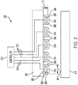
- FIG. 3 a side view illustrates details of an apparatus 300 according to an example embodiment.
- the apparatus includes a transfer substrate 302 with two or more transfer elements 304.
- the transfer elements 304 can selectively made to change stiffness, which can be expressed as the Young's modulus of the material from which the elements are made.
- the Young's modulus is a measure of stress (force per unit area) divided by strain (proportional deformation) in a material in the linear elasticity regime. Generally, materials with higher Young's modulus (lower strain for a stress ⁇ ) is stiffer than a material with lower Young's modules (higher strain for the same ⁇ ).
- Other measures may also be used to represent stiffness of a material, such as storage modulus, which also accounts for dynamic performance of the material.
- Some measures may be used to represent stiffness of a part, such as a spring constant, that may be functionally equivalent in defining performance of the part. However the stiffness is defined, the transfer elements 304 have a change in stiffness in response to temperature that can be utilized in device transfer as described below.
- Each of the transfer elements 304 includes an adhesion element 306 having a higher Young's modulus > 6 MPa at a lower temperature and a lower Young's modulus ⁇ 1 MPa at a higher temperature.
- Each of the transfer elements 304 also includes a thermal element 308 operable to change a temperature of the adhesion element 306 in response to an input, e.g., via inputs 310.
- a controller 312 is coupled to provide the inputs 310 to the thermal elements 308, thereby causing a subset of the transfer elements 304 to selectably pick up and hold objects 314 to and (optionally) release the objects 314 from the transfer substrate 302.
- the objects 314 will not stick to the transfer elements 304 at the lower temperature but will stick at the higher temperature.
- the transfer elements may be cooled before attempting to pull the objects 314 away from transfer substrate 302.
- the apparatus 300 may be part of a micro-transfer system, which is a system used to transfer micro-objects (e.g., 1 ⁇ m to 1 mm) from the transfer substrate 302 to a target substrate 316.
- the adhesion element 306 may be formed of a multi-polymer that contains stearyl acrylate-based (SA).
- SA stearyl acrylate-based
- a difference between the higher and lower temperatures may be less than 20°C (or in other cases less than 50°C) in order to adjust the tackiness of the adhesion element 306 such that there is a marked difference in surface adhesion and Young's modulus, e.g., from ⁇ 1MPa at the higher temperature to > 6MPa at the higher temperature.
- the controller 312 in such as a system may be coupled to actuators that induce relative motion between substrates to facilitate object transfer as described herein.
- the thermal element 308 may include one or both of a heating element and a cooling element.
- the inputs 310 may include electrical signals and/or laser light.
- the inputs 310 may be configured (e.g., using a matrix circuit) such that there are fewer lines going to the controller 312 than the total number of transfer elements 304.
- the transfer elements 304 may further include a thermal insulator 309 between the adhesion element 306 and the transfer substrate 302. The insulator 309 helps prevent heat transfer to the substrate 302, thereby decreasing the amount of energy needed to affect temperature change at the adhesion element 306 and decrease response time.
- the transfer elements 304 form an intermediate transfer surface whose compliance can be modulated (e.g., have a sharp rigid-to-soft transition) as a function of temperature. Such a surface can be used to pick up and release groups of micro-objects in a controlled and selectable manner.
- Each transfer element 304 may have lateral dimensions W from several micrometers to several hundreds of micrometers.
- Each transfer element 304 may have a total thickness T from less than one micron to several hundred microns.
- the pitch of the transfer array may vary from several microns to several millimeters.
- the thermal elements 308 and insulating layers 309 are continuous layers that are not physically isolated from one another.
- the transfer element "pixel" is the region where the heating/cooling elements can be individually addressed and controlled (see FIG 6 ).
- the substrate 302 material may include but is not limited to glass, quartz, silicon, polymer and silicon carbide (SiC).
- the substrate 302 may have a thickness ranges from several tens of microns to several millimeters and lateral dimensions from several millimeters to one meter.
- a single transfer element may be used.
- a single transfer element 304 may be part of a manipulator that is placed at the end of a robotic arm.
- a single transfer element 304 may be used to pick up objects without requiring the use of pincers, vacuum, magnetics, etc.
- one or more transfer elements may be placed at the ends of pincers or other holding appendages to assist in gripping without having to apply undue pressure on the object being held.
- a thermal element can increase change adhesion (corresponding to a change in Young's modulus) during holding and releasing operations.
- Phase-changing polymer comprising stearyl acrylate (SA) has been studied as a bistable electroactive polymer (BSEP) for use in the adhesion element.
- the BSEP polymer is a rigid polymer below its glass transition temperature (Tg). Above Tg, it becomes an elastomer that exhibits large elongation at break and high dielectric field strength. Electrical actuation can be carried out above Tg with the rubbery BSEP functioning as a dielectric elastomer. The deformation is locked when cooling down the polymer below Tg. The shape change can be reversed when the polymer is reheated above Tg.
- SA Stearyl acrylate (octadecyl acrylate, SA) based polymers have been investigated as shape memory polymers due to their sharp phase transition between the crystalline and molten states of the stearyl moieties.
- the abrupt and reversible phase transition of the crystalline aggregates of the stearyl moieties results in a rapid shift between the rigid and rubbery states of the polymers during temperature cycles.
- the transition of SA is typically below 50°C with a narrow phase change temperature range of less than 20°C. Therefore, SA is an ideal component for imparting a sharp rigid-to-rubbery transition.
- the adhesion element 306 may be made of materials including but not limited to stearyl acrylate (octadecyl acrylate, SA) based polymers, stearyl acrylate and urethane diacrylate copolymer or other types of polymers. In particular, a copolymer containing urethane diacrylate and SA has been found to have desirable characteristics for these purposes.
- the adhesion element 306 preferably has a sharp rigid-to-soft transition therefore the adhesion can be easily modulated with temperature change.
- the thermal elements 308 could be thermoelectric heating/cooling elements, resistive heaters, diode heaters, inductive heating elements, an optical heating elements, etc.
- the thermal elements 308 may include thin film resistors, a diode structure, and/or or high optical energy absorbing efficiency materials such as carbon black, carbon nanotubes, engineered nanoparticles, etc.
- the thermal insulator 309 may be made from materials such as polyimide, PDMS, parylene, glass, silicon oxide, Al x O y and SxNy, and combinations thereof.
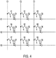
- the transfer substrate 302 contains an active electronics components array and the thermal elements 308 may be interconnected with them in a grid. This is shown schematically shown in FIG. 4 and 5 .
- the 2D array of thermal elements can be controlled by a diode as shown in FIG. 4 or a transistor as shown in FIG. 5 .
- heating elements R1-R9 are controlled by a matrix of diodes D1-D9. This may be referred to as passive switching matrix, which reduces the number of electrical wires needed to connect the heating elements to controller chip.
- the heating elements are addressed row-by-row.
- R1 can be biased to 0V
- R2 and R3 are biased to 5V.
- the C1, C2 and C3 bias voltages will determine if the heating elements R1, R2 or R3 is turned on (column is biased to 5V) or off (column line is biased to 0V). All the other heaters are off because of diodes blocking the current flow.
- the process is repeated for all the rest of rows for selected row is biased to 0V and all the other rows biased to 5V.
- the thermal time constant of thermal elements will be designed to be longer than the "frame rate" of the 2D scanning to ensure quasi constant temperature is maintained for each addressable transfer.
- the schematic diagram in FIG. 5 shows another circuit where the thermal elements are controlled by transistors (e.g., thin film transistors, or TFTs) instead of diode, which may be referred to as "active matrix switching.”
- TFTs thin film transistors
- Each thermal element has at least one end connected to a drain or a source of one of the TFTs.
- the advantage of using transistors is that larger voltage range and better isolation can be achieved. In this case, all the rows not selected will be biased to, e.g. -5V, to turn off transistors. When a row is selected, the row line is biased to, e.g. 20V, to turn on the transistors. Biasing the column line to the specific voltage enables the corresponding heating element of the selected row to be heated to the desired temperature. Similar to the embodiment in FIG. 4 , the process will be repeated for the rest of the other rows.
- transistors e.g., thin film transistors, or TFTs
- a side view shows a transfer substrate 602 according to another example embodiment.
- the transfer substrate 602 has two or more transfer elements 604 each including an adhesion element 606 having a surface adhesion that varies by temperature.
- Each of the transfer elements 604 also includes a thermal element 608 operable to change a temperature of the regional adhesion element 606 (e.g., part of element near thermal element 608) in response to an input.
- the adhesion element 604 is part of a continuous layer that covers more than one transfer element 604, in this case, all of the illustrated elements 604. Any of the embodiments described herein may use an adhesion element formed of a single layer that covers a plurality of element similar to what is shown in FIG. 6 .
- this embodiment shows the use of an insulator 609 between the transfer elements 604 and the substrate 602, although such insulators 609 may be optional.
- one or both of the thermal elements 608 and insulator 609 may be implemented as a single layer that covers more than one transfer element 604.
- individual signal lines e.g., lines 310 in FIG. 3 and/or waveguides 1112 in FIG. 7
- a side view shows a transfer substrate 702 according to another example embodiment.
- the transfer substrate 702 has two or more transfer elements 704 each including an adhesion element 706 having a surface adhesion that varies by temperature.
- Each of the transfer elements 704 also includes a thermal element 708 operable to change a temperature of the adhesion element 706 in response to an input.
- the thermal elements 708 are activated by laser light 710 which is delivered via waveguides 712 in the substrate 702. The light is provided from one or more lasers 716 and may selectively activate the transfer elements 704 via optical switching elements 714 that absorb or redirect light away from transfer elements that are not to be heated.
- multiple lasers 716 may be used, as many as one per transfer element and they may be integrated in the substrate 702 or mounted externally.
- the optical switches 714 may be electrically activated and may be arranged in a matrix similar to the diodes and transistors shown in FIGS. 4 and 5 to reduce the number of lines to the controller.
- a side view shows a transfer substrate 802 according to another example embodiment.
- the transfer substrate 802 has two or more transfer elements 804 each including an adhesion element 806 having a surface adhesion that varies by temperature.
- Each of the transfer elements 804 also includes a thermal element 808 operable to change a temperature of the adhesion element 806 in response to an input.
- Each of the transfer elements 804 also includes an insulator 809 that thermally insulates the thermal element 808 from the transfer substrate 802.
- the transfer substrate 802 is curved and mounted to a roller 813 that rotates relative to a target substrate 816.
- the roller 813 and target substrate also move linearly relative to one another (horizontally in this illustration) such that only a subset of the transfer elements 804 (e.g., a single element 804) contacts the transfer substrate 816 at a time.
- the subset of transfer elements 804 are selectively activated to hold or release an object 814, such that some of the objects 814 are selectively transferred to the target substrate 816.
- the shaded object 814 to the left was not transferred to the target substrate 816.
- Note another part of the roller 813 and substrate 802 may be in contact with a donor substrate (not shown) such that the transfer of objects may be a rolling transfer process where objects 814 are picked up from the donor and transferred to the target 816.
- the roller 813 and substrate 802 may be in contact with the donor and target substrates at the same times, or different times.
- a second transfer substrate (not shown) may be used to deposit discarded objects 814, and this second transfer substrate may also use a curved substrate.
- Any of the other embodiments described herein may use a curved transfer substrate and rolling transfer process as shown in FIG. 8 .
- the transfer may be facilitated by a rotational actuator 820 that rotates the roller 813 and a linear actuator 821 that induces relative linear motion between the roller 813 and the substrate 802.
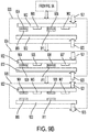
- FIGS. 9A and 9B a block diagram shows a method according to an example embodiment.
- a transfer substrate 902 is shown having an array of transfer elements 904-907.
- the transfer substrate 902 is shown positioned over a donor substrate 908 such that the array of transfer elements 904-907 is aligned over respective objects 909-912.
- the objects 909, 911 form a subset of the objects 909-912 that is intended to be transferred off the donor substrate 908.
- the transfer substrate 902 is moved towards the donor substrate 908, or vice versa. This movement may be accomplished via one or more mechanical actuators 901, 903 that induce relative motion between the substrates 902, 908.
- each transfer element 904, 906 in the subset is at or above a high temperature (e.g., between 30°C and 65°C) such that an adhesion element of each transfer element 904, 906 in the subset achieves a lower Young's modulus (e.g., ⁇ 1 MPa).
- This input may be applied before or after the subset of transfer elements 904, 906 contact the respective subset of objects 909, 911.
- the subset of objects 909, 911 are attracted to (e.g., due to increased van der Waals forces at the lower Young's modulus) to the subset of the transfer elements 904, 906 that are at the lower Young's modulus that correspond to the higher temperature range.
- the actuators 902, 903 may be configured to apply pressure during this operation
- transfer elements 905, 907 that are not in the subset of transfer elements 904, 906 may be at or below a lower temperature (e.g., between 0°C and 30°C) that results in transfer elements 905, 907 having a higher Young's modulus (e.g., > 6 MPa, and in some cases > 10 MPa). At this second Young's modulus, the other transfer elements 905, 907 will not be attracted to respective objects 910, 912, e.g., due to low van der Waals forces. Note that in the previous step shown in block 900, the transfer elements 904-907 may be at any temperature.
- the subset of transfer elements 904, 906 has been set at or below the lower temperature while still in keep in good contact with the subsets of objects 909, 911 that will be transferred off the substrate 908. It has been found that this can increase attraction between the transfer elements 904, 906 and objects 909, 911. This attraction may be further enhanced by adding protrusions to the objects 909, 911 that extend from a surface of the objects 909, 911 that face the transfer elements 904.
- the transfer substrate 902 is moved away from the donor substrate by one or more of the actuators 901, 903, causing the subset of objects 909, 911 to be separated from the donor substrate 908 while the other objects 910, 912 remain on the donor substrate.
- the transfer substrate 902 is aligned with and moved towards a target substrate 922 by actuators 921, 923, which may be the same or different than actuators 901, 903 in FIG. 9A .
- the subset of objects 909, 911 on the transfer substrate 902 contact the target substrate 922.
- second inputs may be applied to the subset of transfer elements 904, 906 causing each transfer element in the subset to achieve or go beyond the higher temperature.
- a counter force may be applied from the target substrate 922 that includes but not limited to adhesive force, electrical force, magnetic force, and a vacuum-created force.
- the transferred objects may include features that increase the adhesion at the time of removal from the donor substrate.
- FIG. 10 diagrams illustrate features of objects 1000-1002 according to example embodiments.
- the objects 1000-1002 are shown on respective substrates 1004-1006.
- Each of the objects 1000-1002 each have one or more respective protrusions 1000a-1002a extending above planar surfaces 1000b-1002b.
- the protrusions may include posts, pyramid, trapezoids, and may include any other type of protruding structure, such as hooks loops, bumps, etc.
- the highest point of the protrusions 1000a-1002a may be between 1 ⁇ m and 20 ⁇ m above the planar surfaces 1000b-1002b.
- the protrusions 1000a-1002a can be made of the same or different materials than that of the objects 1000-1002, such as silicon, GaN, SiO2, SiN, metal, SU8, polyimide or other polymer.
- the substrates 1004-1006 may be donor substrates that have holding layers 1004a-1006a configured to temporarily hold the objects 1000-1002.
- the temporary holding layers 1004a-1006a may include an elastomer material such as polydimethylsiloxane (PDMS), silicone gel, etc., and may have a Young's modulus ⁇ 2MPa.
- the thickness of the layers 1004a-1006a may range from 1 ⁇ m to 100 ⁇ m.
Landscapes
- Micromachines (AREA)
- Die Bonding (AREA)
- Container, Conveyance, Adherence, Positioning, Of Wafer (AREA)
Abstract
Description
- The present disclosure is directed to selectable surface adhesion elements with selectable sharp rigid-to-soft transitions. In one embodiment, an apparatus includes a transfer substrate with two or more transfer elements. Each of the transfer elements includes an adhesion element having a higher Young's modulus at a lower temperature and a lower Young's modulus at a higher temperature. The apparatus includes a heating element operable to change an operating temperature of the adhesion element in response to an input. A controller is coupled to provide the inputs to the heating elements of the two or more transfer elements to cause a change in temperature at least between the higher and lower temperature. The change in temperature causes the transfer elements to selectably hold objects to and release the objects from the transfer substrate in response to changes between the higher and lower Young's moduli of transfer elements.
- In another embodiment, a method involves applying first inputs to a plurality of transfer elements on a transfer substrate. Each of the plurality of transfer elements has a higher Young's modulus at a lower temperature and a lower Young's modulus at a higher temperature. The first inputs cause the subset of transfer elements to be at or above the higher temperature. The transfer elements are caused to contact a respective plurality of objects on a donor substrate at or above the higher temperature. The transfer elements are cooled to at or below the lower temperature while in contact with the plurality of objects. The transfer substrate is moved away from the donor substrate, the subset of objects adhere to the subset of transfer elements and move with the transfer substrate. The objects on the transfer substrate are caused to contact a target substrate and the subset of objects transferried from the transfer substrate to the target substrate.
- In another embodiment, a system includes a donor substrate with a plurality of objects disposed on a holding layer comprising one or more of polydimethylsiloxane and silicone gel. A transfer substrate has two or more transfer elements. Each of the transfer elements includes an adhesion element having a higher Young's modulus at a lower temperature and a lower Young's modulus at a higher temperature. Each transfer element has a heating element operable to change an operating temperature of the adhesion element in response to an input. A controller is coupled to selectively provide the inputs to the heating elements of the two or more transfer elements to cause a subset of the transfer elements to selectably lift the objects from the donor substrate in response to changes at least between the higher and lower temperatures. The system includes one or more actuators configured to move one or both of the donor substrate and transfer substrate to facilitate lifting the objects from the donor substrate.
- These and other features and aspects of various embodiments may be understood in view of the following detailed discussion and accompanying drawings.
- The discussion below makes reference to the following figures, wherein the same reference number may be used to identify the similar/same component in multiple figures. The drawings are not necessarily to scale.
-
FIGS. 1 and 2 are block diagrams showing an assembly process according to an example embodiment; -
FIG. 3 is a side view of an apparatus according to an example embodiment; -
FIGS. 4 and5 are schematic diagrams of switching matrices for a transfer substrate according to example embodiments; -
FIG 6 is a side view of a transfer substrates according to an example embodiment; -
FIGS 7 and8 are side views of transfer substrates according to various example embodiments; -
FIGS. 9A and9B are diagrams of a method according to an example embodiment; and -
FIG. 10 is a diagram showing protrusions on transferable objects according to example embodiments. - The present disclosure relates to manipulation and assembly of objects, and in some embodiments the mass assembly of micro-objects via a transfer substrate. Some electronic devices are fabricated by mechanically overlaying small objects on top of each other. While micro-electronic and micro-optical components are sometimes manufactured using wafer formation techniques such as layer deposition, masking, and etching, certain classes of materials are not growth-compatible with each other. In such a case, the assembly may involve forming one class of devices on a first substrate and a second class of devices on a second substrate, and then mechanically joining them, e.g., via flip-chip or transfer printing techniques.
- Aspects described herein relate to a system that is capable of transferring large number of micro objects (e.g., particles, chiplets, mini/micro-LED dies) from a donor substrate to another substrate in parallel while maintaining high position registration of the individual micro objects. This system allows selectively transferring of micro objects from a transfer substrate and selectively place the micro objects to the destination or target substrate. This system may be used for assembling devices such as microLED displays.
- Generally, microLED displays are made with arrays of microscopic LEDs forming the individual transfer elements. Both OLED displays and microLED displays offer greatly reduced energy requirements compared to conventional LCD systems. Unlike OLED, microLED is based on conventional GaN LED technology, which offers higher total brightness than OLED produces, as well as higher efficiency in terms of light emitted per unit of power. It also does not suffer from the shorter lifetimes of OLED.
- A single 4K television utilizing microLED has ∼25 million small LED subpixels that then need to be assembled. Mass transfer of chiplets is one technology that may be used for microLED manufacturing. Transferring microLED to a target backplane quickly and accurately with a high yield will be one of the techniques that manufacturers need to perfect in order for microLED to be a viable mass-market product. The techniques described below can be used for microLED manufacture, as well as other assembly procedures in which a large number of (typically) small objects need to be moved at once, and where it may be necessary to selectively move a subset of such device to and/or from the transfer media. Such micro objects may include but not limited to inks, pre-deposited metal films, silicon chips, integrated circuit chips, beads, microLED dies, micro-electromechanical system (MEMS) structures, and any other pre-fabricated micro structures.
- Being able to selectively transfer chiplets in an arbitrary pattern is useful to facilitate the effective transfer process, pixel repair, hole/vacancy refill for microLED display manufacturing, which will lead to high process yield. An elastomer stamp has been used to deterministically transfer microscale LED chips for this type of application. However, an elastomer stamp has fixed pattern and cannot transfer arbitrary pattern of chiplets. Inevitably, some subset of the chiplets will be defective, and therefore it becomes difficult to replace a select few of them using such a stamp.
- In
FIGS. 1 and 2 , block diagrams show an example of an assembly process that can be achieved using devices, systems, and methods according to an example embodiment. InFIG. 1 , a donor wafer/substrate 100 is shown that includes an array ofchiplets 101 that may have been grown or placed on thesubstrate 100. The shaded chiplets in thearray 101 have been identified as defective, and when the chiplets are transferred to atarget substrate 102, only asubset 101a of the chiplet array are transferred, namely the good chiplets that are not shaded. This may be achieved with atransfer substrate 200 as shown inFIG. 2 that can selectively pick up just thesubset 101a from thedonor substrate 100 once they are identified. As shown inFIG. 2 , thetransfer substrate 202 subsequently picks up a second set of chiplets 200 (e.g., from a different donor substrate). The locations of the chiplets within theset 200 correspond to the locations of the defective chiplets on thefirst donor substrate 100. Thetransfer substrate 202 moves thisset 200 to thetarget substrate 102, resulting in afull set 201 of operational chiplets being located on thetarget substrate 102. - The present disclosure relates to, among other things, a transfer substrate with a set of transfer elements (e.g., transfer pixels) that can selectively hold a subset of micro objects. Thus, even when all of the transfer elements are in contact with an array of micro objects that is greater than the subset, only the subset will be adhere and be transferred, and the objects outside the subset will be left behind or otherwise unaffected. Similarly, the transfer substrate may be able to selectively release a subset of micro objects that are currently attached to the substrate, such that only the subset is transferred to a target even all of the transfer elements are currently holding a micro object. This process is repeatable and reversible, such that no permanent bonding is need to affect the selective holding or releasing of the objects.
- In
FIG. 3 , a side view illustrates details of anapparatus 300 according to an example embodiment. The apparatus includes atransfer substrate 302 with two ormore transfer elements 304. Thetransfer elements 304 can selectively made to change stiffness, which can be expressed as the Young's modulus of the material from which the elements are made. The Young's modulus is a measure of stress (force per unit area) divided by strain (proportional deformation) in a material in the linear elasticity regime. Generally, materials with higher Young's modulus (lower strain for a stress σ) is stiffer than a material with lower Young's modules (higher strain for the same σ). Other measures may also be used to represent stiffness of a material, such as storage modulus, which also accounts for dynamic performance of the material. Some measures may be used to represent stiffness of a part, such as a spring constant, that may be functionally equivalent in defining performance of the part. However the stiffness is defined, thetransfer elements 304 have a change in stiffness in response to temperature that can be utilized in device transfer as described below. - Each of the
transfer elements 304 includes anadhesion element 306 having a higher Young's modulus > 6 MPa at a lower temperature and a lower Young's modulus < 1 MPa at a higher temperature. Each of thetransfer elements 304 also includes athermal element 308 operable to change a temperature of theadhesion element 306 in response to an input, e.g., viainputs 310. Acontroller 312 is coupled to provide theinputs 310 to thethermal elements 308, thereby causing a subset of thetransfer elements 304 to selectably pick up and holdobjects 314 to and (optionally) release theobjects 314 from thetransfer substrate 302. In particular, theobjects 314 will not stick to thetransfer elements 304 at the lower temperature but will stick at the higher temperature. To increase the reliability of the adhesion, the transfer elements may be cooled before attempting to pull theobjects 314 away fromtransfer substrate 302. - The
apparatus 300 may be part of a micro-transfer system, which is a system used to transfer micro-objects (e.g., 1 µm to 1 mm) from thetransfer substrate 302 to atarget substrate 316. Theadhesion element 306 may be formed of a multi-polymer that contains stearyl acrylate-based (SA). In such a case, a difference between the higher and lower temperatures may be less than 20°C (or in other cases less than 50°C) in order to adjust the tackiness of theadhesion element 306 such that there is a marked difference in surface adhesion and Young's modulus, e.g., from < 1MPa at the higher temperature to > 6MPa at the higher temperature. Thecontroller 312 in such as a system may be coupled to actuators that induce relative motion between substrates to facilitate object transfer as described herein. - The
thermal element 308 may include one or both of a heating element and a cooling element. Theinputs 310 may include electrical signals and/or laser light. Theinputs 310 may be configured (e.g., using a matrix circuit) such that there are fewer lines going to thecontroller 312 than the total number oftransfer elements 304. Thetransfer elements 304 may further include athermal insulator 309 between theadhesion element 306 and thetransfer substrate 302. Theinsulator 309 helps prevent heat transfer to thesubstrate 302, thereby decreasing the amount of energy needed to affect temperature change at theadhesion element 306 and decrease response time. - Generally, the
transfer elements 304 form an intermediate transfer surface whose compliance can be modulated (e.g., have a sharp rigid-to-soft transition) as a function of temperature. Such a surface can be used to pick up and release groups of micro-objects in a controlled and selectable manner. Eachtransfer element 304 may have lateral dimensions W from several micrometers to several hundreds of micrometers. Eachtransfer element 304 may have a total thickness T from less than one micron to several hundred microns. The pitch of the transfer array may vary from several microns to several millimeters. In some embodiment, thethermal elements 308 and insulatinglayers 309 are continuous layers that are not physically isolated from one another. As such, the transfer element "pixel" is the region where the heating/cooling elements can be individually addressed and controlled (seeFIG 6 ). Thesubstrate 302 material may include but is not limited to glass, quartz, silicon, polymer and silicon carbide (SiC). Thesubstrate 302 may have a thickness ranges from several tens of microns to several millimeters and lateral dimensions from several millimeters to one meter. - Note that, while the illustrated embodiments show two or
more transfer elements 304, in some cases a single transfer element may be used. For example, asingle transfer element 304 may be part of a manipulator that is placed at the end of a robotic arm. In such a configuration, asingle transfer element 304 may be used to pick up objects without requiring the use of pincers, vacuum, magnetics, etc. In other configurations, one or more transfer elements may be placed at the ends of pincers or other holding appendages to assist in gripping without having to apply undue pressure on the object being held. As with the other embodiments, a thermal element can increase change adhesion (corresponding to a change in Young's modulus) during holding and releasing operations. - Phase-changing polymer comprising stearyl acrylate (SA) has been studied as a bistable electroactive polymer (BSEP) for use in the adhesion element. The BSEP polymer is a rigid polymer below its glass transition temperature (Tg). Above Tg, it becomes an elastomer that exhibits large elongation at break and high dielectric field strength. Electrical actuation can be carried out above Tg with the rubbery BSEP functioning as a dielectric elastomer. The deformation is locked when cooling down the polymer below Tg. The shape change can be reversed when the polymer is reheated above Tg.
- Stearyl acrylate (octadecyl acrylate, SA) based polymers have been investigated as shape memory polymers due to their sharp phase transition between the crystalline and molten states of the stearyl moieties. The abrupt and reversible phase transition of the crystalline aggregates of the stearyl moieties results in a rapid shift between the rigid and rubbery states of the polymers during temperature cycles. The transition of SA is typically below 50°C with a narrow phase change temperature range of less than 20°C. Therefore, SA is an ideal component for imparting a sharp rigid-to-rubbery transition. Some preliminary experiments have been done to validate this characteristic.
- The
adhesion element 306 may be made of materials including but not limited to stearyl acrylate (octadecyl acrylate, SA) based polymers, stearyl acrylate and urethane diacrylate copolymer or other types of polymers. In particular, a copolymer containing urethane diacrylate and SA has been found to have desirable characteristics for these purposes. Theadhesion element 306 preferably has a sharp rigid-to-soft transition therefore the adhesion can be easily modulated with temperature change. Thethermal elements 308 could be thermoelectric heating/cooling elements, resistive heaters, diode heaters, inductive heating elements, an optical heating elements, etc. Thethermal elements 308 may include thin film resistors, a diode structure, and/or or high optical energy absorbing efficiency materials such as carbon black, carbon nanotubes, engineered nanoparticles, etc. Thethermal insulator 309 may be made from materials such as polyimide, PDMS, parylene, glass, silicon oxide, AlxOy and SxNy, and combinations thereof. - In one embodiment, the
transfer substrate 302 contains an active electronics components array and thethermal elements 308 may be interconnected with them in a grid. This is shown schematically shown inFIG. 4 and5 . The 2D array of thermal elements (resistors in these examples) can be controlled by a diode as shown inFIG. 4 or a transistor as shown inFIG. 5 . In the embodiment shown inFIG. 4 , heating elements R1-R9 are controlled by a matrix of diodes D1-D9. This may be referred to as passive switching matrix, which reduces the number of electrical wires needed to connect the heating elements to controller chip. - In this case, the heating elements are addressed row-by-row. For example, R1 can be biased to 0V, while R2 and R3 are biased to 5V. The C1, C2 and C3 bias voltages will determine if the heating elements R1, R2 or R3 is turned on (column is biased to 5V) or off (column line is biased to 0V). All the other heaters are off because of diodes blocking the current flow. The process is repeated for all the rest of rows for selected row is biased to 0V and all the other rows biased to 5V. The thermal time constant of thermal elements will be designed to be longer than the "frame rate" of the 2D scanning to ensure quasi constant temperature is maintained for each addressable transfer.
- The schematic diagram in
FIG. 5 shows another circuit where the thermal elements are controlled by transistors (e.g., thin film transistors, or TFTs) instead of diode, which may be referred to as "active matrix switching." Each thermal element has at least one end connected to a drain or a source of one of the TFTs. The advantage of using transistors is that larger voltage range and better isolation can be achieved. In this case, all the rows not selected will be biased to, e.g. -5V, to turn off transistors. When a row is selected, the row line is biased to, e.g. 20V, to turn on the transistors. Biasing the column line to the specific voltage enables the corresponding heating element of the selected row to be heated to the desired temperature. Similar to the embodiment inFIG. 4 , the process will be repeated for the rest of the other rows. - In
FIG. 6 , a side view shows atransfer substrate 602 according to another example embodiment. As with the embodiment inFIG. 3 , thetransfer substrate 602 has two ormore transfer elements 604 each including anadhesion element 606 having a surface adhesion that varies by temperature. Each of thetransfer elements 604 also includes athermal element 608 operable to change a temperature of the regional adhesion element 606 (e.g., part of element near thermal element 608) in response to an input. In this example, theadhesion element 604 is part of a continuous layer that covers more than onetransfer element 604, in this case, all of the illustratedelements 604. Any of the embodiments described herein may use an adhesion element formed of a single layer that covers a plurality of element similar to what is shown inFIG. 6 . - Also note that this embodiment shows the use of an
insulator 609 between thetransfer elements 604 and thesubstrate 602, althoughsuch insulators 609 may be optional. Also, as indicated by dashed lines, one or both of thethermal elements 608 andinsulator 609 may be implemented as a single layer that covers more than onetransfer element 604. In such an embodiment, individual signal lines (e.g.,lines 310 inFIG. 3 and/or waveguides 1112 inFIG. 7 ) may be attached to thethermal element layer 608, such that local temperature change is induced within a region that defines the size and location of theindividual transfer element 608. - In
FIG. 7 , a side view shows atransfer substrate 702 according to another example embodiment. As with the embodiment inFIG. 3 , thetransfer substrate 702 has two ormore transfer elements 704 each including anadhesion element 706 having a surface adhesion that varies by temperature. Each of thetransfer elements 704 also includes athermal element 708 operable to change a temperature of theadhesion element 706 in response to an input. In this example, thethermal elements 708 are activated bylaser light 710 which is delivered viawaveguides 712 in thesubstrate 702. The light is provided from one or more lasers 716 and may selectively activate thetransfer elements 704 viaoptical switching elements 714 that absorb or redirect light away from transfer elements that are not to be heated. Note that multiple lasers 716 may be used, as many as one per transfer element and they may be integrated in thesubstrate 702 or mounted externally. Theoptical switches 714 may be electrically activated and may be arranged in a matrix similar to the diodes and transistors shown inFIGS. 4 and5 to reduce the number of lines to the controller. - In
FIG. 8 , a side view shows atransfer substrate 802 according to another example embodiment. As with the embodiment inFIG. 3 , thetransfer substrate 802 has two ormore transfer elements 804 each including anadhesion element 806 having a surface adhesion that varies by temperature. Each of thetransfer elements 804 also includes athermal element 808 operable to change a temperature of theadhesion element 806 in response to an input. Each of thetransfer elements 804 also includes aninsulator 809 that thermally insulates thethermal element 808 from thetransfer substrate 802. - In this embodiment, the
transfer substrate 802 is curved and mounted to aroller 813 that rotates relative to atarget substrate 816. Theroller 813 and target substrate also move linearly relative to one another (horizontally in this illustration) such that only a subset of the transfer elements 804 (e.g., a single element 804) contacts thetransfer substrate 816 at a time. The subset oftransfer elements 804 are selectively activated to hold or release anobject 814, such that some of theobjects 814 are selectively transferred to thetarget substrate 816. Note that theshaded object 814 to the left was not transferred to thetarget substrate 816. Note another part of theroller 813 andsubstrate 802 may be in contact with a donor substrate (not shown) such that the transfer of objects may be a rolling transfer process whereobjects 814 are picked up from the donor and transferred to thetarget 816. - The
roller 813 andsubstrate 802 may be in contact with the donor and target substrates at the same times, or different times. In such a case, a second transfer substrate (not shown) may be used to deposit discardedobjects 814, and this second transfer substrate may also use a curved substrate. Any of the other embodiments described herein may use a curved transfer substrate and rolling transfer process as shown inFIG. 8 . As indicated byarrows rotational actuator 820 that rotates theroller 813 and alinear actuator 821 that induces relative linear motion between theroller 813 and thesubstrate 802. - In
FIGS. 9A and9B , a block diagram shows a method according to an example embodiment. Inblock 900, atransfer substrate 902 is shown having an array of transfer elements 904-907. Thetransfer substrate 902 is shown positioned over adonor substrate 908 such that the array of transfer elements 904-907 is aligned over respective objects 909-912. As indicated by the shading, theobjects donor substrate 908. Thetransfer substrate 902 is moved towards thedonor substrate 908, or vice versa. This movement may be accomplished via one or moremechanical actuators substrates - As seen in
block 916, when contact is made between the transfer elements 904-907 and objects 909-912, electrical inputs have been applied to a subset of thetransfer elements elements transfer element transfer element transfer elements objects objects transfer elements actuators - Note that
other transfer elements transfer elements transfer elements other transfer elements respective objects block 900, the transfer elements 904-907 may be at any temperature. - As seen in
block 918, the subset oftransfer elements objects substrate 908. It has been found that this can increase attraction between thetransfer elements objects objects objects transfer elements 904. - As seen in
block 919, thetransfer substrate 902 is moved away from the donor substrate by one or more of theactuators objects donor substrate 908 while theother objects block 920 inFIG. 9B , thetransfer substrate 902 is aligned with and moved towards atarget substrate 922 byactuators actuators FIG. 9A . As seen inblock 924, the subset ofobjects transfer substrate 902 contact thetarget substrate 922. - Optionally, in one or both of
blocks transfer elements objects target substrate 922 such that theobjects target substrate 922 that includes but not limited to adhesive force, electrical force, magnetic force, and a vacuum-created force. - As noted above, the transferred objects may include features that increase the adhesion at the time of removal from the donor substrate. In
FIG. 10 , diagrams illustrate features of objects 1000-1002 according to example embodiments. The objects 1000-1002 are shown on respective substrates 1004-1006. Each of the objects 1000-1002 each have one or morerespective protrusions 1000a-1002a extending aboveplanar surfaces 1000b-1002b. As shown, the protrusions may include posts, pyramid, trapezoids, and may include any other type of protruding structure, such as hooks loops, bumps, etc. The highest point of theprotrusions 1000a-1002a may be between 1µm and 20µm above theplanar surfaces 1000b-1002b. Theprotrusions 1000a-1002a can be made of the same or different materials than that of the objects 1000-1002, such as silicon, GaN, SiO2, SiN, metal, SU8, polyimide or other polymer. - The substrates 1004-1006 may be donor substrates that have holding
layers 1004a-1006a configured to temporarily hold the objects 1000-1002. Thetemporary holding layers 1004a-1006a may include an elastomer material such as polydimethylsiloxane (PDMS), silicone gel, etc., and may have a Young's modulus < 2MPa. The thickness of thelayers 1004a-1006a may range from 1 µm to 100 µm. - Unless otherwise indicated, all numbers expressing feature sizes, amounts, and physical properties used in the specification and claims are to be understood as being modified in all instances by the term "about." Accordingly, unless indicated to the contrary, the numerical parameters set forth in the foregoing specification and attached claims are approximations that can vary depending upon the desired properties sought to be obtained by those skilled in the art utilizing the teachings disclosed herein. The use of numerical ranges by endpoints includes all numbers within that range (e.g. 1 to 5 includes 1, 1.5, 2, 2.75, 3, 3.80, 4, and 5) and any range within that range.
- The various embodiments described above may be implemented using circuitry, firmware, and/or software modules that interact to provide particular results. One of skill in the arts can readily implement such described functionality, either at a modular level or as a whole, using knowledge generally known in the art. For example, the flowcharts and control diagrams illustrated herein may be used to create computer-readable instructions/code for execution by a processor. Such instructions may be stored on a non-transitory computer-readable medium and transferred to the processor for execution as is known in the art. The structures and procedures shown above are only a representative example of embodiments that can be used to provide the functions described hereinabove.
- The foregoing description of the example embodiments has been presented for the purposes of illustration and description. It is not intended to be exhaustive or to limit the embodiments to the precise form disclosed. Many modifications and variations are possible in light of the above teaching. Any or all features of the disclosed embodiments can be applied individually or in any combination are not meant to be limiting, but purely illustrative. It is intended that the scope of the invention be limited not with this detailed description, but rather determined by the claims appended hereto.
Claims (22)
- An apparatus, comprising:a transfer substrate, comprising two or more transfer elements, each of the transfer elements comprising:an adhesion element having a higher Young's modulus at a lower temperature and a lower Young's modulus at a higher temperature;a heating element operable to change an operating temperature of the adhesion element in response to an input; anda controller coupled to provide the inputs to the heating elements of the two or more transfer elements to cause a change in temperature at least between the higher and lower temperature, the change in temperature causing the transfer elements to selectably hold objects to and release the objects from the transfer substrate in response to changes between the higher and lower Young's moduli of transfer elements.
- The apparatus of claim 1, wherein the Young's modulus is > 6MPa at the lower temperature and < 1MPa at the higher temperature, and wherein the difference between the lower temperature and the higher temperature is less than 50°C.
- The apparatus of claim 1, wherein the substrate comprises one or more of glass and silicon carbide.
- The apparatus of claim 1, wherein the objects comprise sub-millimeter electronic devices.
- The apparatus of claim 1, wherein the adhesion element is formed of a copolymer containing at least one of urethane diacrylate, stearyl acrylate, poly(norbornene), poly(urethane) and poly(styrene-butadiene).
- The apparatus of claim 1, wherein the heating element comprises a resistive heating element.
- The apparatus of claim 1, further comprising a plurality of active electronic components coupled to the controller and configured to independently active respective ones of the heating elements.
- The apparatus of claim 7, wherein the active electronic components comprise diodes, each heating element having at least one end connected to one of the diodes.
- The apparatus of claim 7, wherein the active electronic components comprise thin film transistors, each heating element having at least one end connected to a drain or a source of one of the thin film transistors.
- The apparatus of claim 1, wherein the objects comprise GaN micro-light emitting diode (LED) chips having a planar surface facing the transfer substrate.
- The apparatus of claim 10, wherein the GaN micro-LED chips comprise one or more protrusions extending above the planar surface.
- The apparatus of claim 11, wherein a highest point of the protrusions is between 1um and 20um above the planar surface.
- The apparatus of claim 11, wherein the protrusions are made of at least one of silicon, GaN, SiO2, SiN, metal, SU8, polyimide or other polymer.
- A method comprising:applying first inputs to a plurality of transfer elements on a transfer substrate, each of the plurality of transfer elements having a higher Young's modulus at a lower temperature and a lower Young's modulus at a higher temperature, the first inputs causing the subset of transfer elements to be at or above the higher temperature;causing the transfer elements to contact a respective plurality of objects on a donor substrate at or above the higher temperature;cooling the transfer elements to at or below the lower temperature while in contact with the plurality of objects;moving the transfer substrate away from the donor substrate, the subset of objects adhering to the subset of transfer elements and moving with the transfer substrate;causing the objects on the transfer substrate to contact a target substrate; andtransferring the subset of objects from the transfer substrate to the target substrate.
- The method of claim 14, wherein causing the transfer elements to contact the objects comprises causing a second plurality of transfer elements on the transfer substrate to contact a second plurality of objects on the donor substrate while the second plurality of transfer elements are below the higher temperature such that the second plurality of objects do not adhere to the transfer substrate and do not move with the transfer substrate.
- The method of claim 14, wherein the higher temperature is between 30°C and 65°C.
- The method of claim 14, wherein the lower temperature is between 0°C and 30°C.
- The method of claim 14, wherein the objects comprise GaN micro-light emitting diode (LED) chips having a planar surface facing the transfer substrate.
- The method of claim 18, wherein the GaN micro-LED chips comprise one or more protrusions extending above the planar surface and wherein a highest point of the protrusions is between 1um and 20um above the planar surface.
- The method of claim 19, wherein the protrusions are made of at least one of silicon, GaN, SiO2, SiN, metal, SU8, polyimide or other polymer.
- A system, comprising:a donor substrate comprising a plurality of objects disposed on a holding layer comprising one or more materials having a Young's modulus < 2MPa.a transfer substrate, comprising two or more transfer elements, each of the transfer elements comprising:an adhesion element having a higher Young's modulus at a lower temperature and a lower Young's modulus at a higher temperature; anda heating element operable to change an operating temperature of the adhesion element in response to an input;a controller coupled to selectively provide the inputs to the heating elements of the two or more transfer elements to cause a subset of the transfer elements to selectably lift the objects from the donor substrate in response to changes at least between the higher and lower temperatures; andone or more actuators configured to move one or both of the donor substrate and transfer substrate to facilitate lifting the objects from the donor substrate.
- The system of claim 21, wherein the holding layer is made of at least one of polydimethylsiloxane and silicone gel and has a thickness from 1 µm to 100 µm.
Applications Claiming Priority (1)
| Application Number | Priority Date | Filing Date | Title |
|---|---|---|---|
| US16/681,215 US11302561B2 (en) | 2019-11-12 | 2019-11-12 | Transfer elements that selectably hold and release objects based on changes in stiffness |
Publications (2)
| Publication Number | Publication Date |
|---|---|
| EP3823011A1 true EP3823011A1 (en) | 2021-05-19 |
| EP3823011B1 EP3823011B1 (en) | 2023-07-05 |
Family
ID=73039945
Family Applications (1)
| Application Number | Title | Priority Date | Filing Date |
|---|---|---|---|
| EP20204793.2A Active EP3823011B1 (en) | 2019-11-12 | 2020-10-29 | Transfer elements that selectably hold and release objects based on changes in stiffness |
Country Status (6)
| Country | Link |
|---|---|
| US (1) | US11302561B2 (en) |
| EP (1) | EP3823011B1 (en) |
| JP (1) | JP7519267B2 (en) |
| KR (1) | KR102647518B1 (en) |
| CN (1) | CN112864046B (en) |
| TW (1) | TWI845786B (en) |
Families Citing this family (7)
| Publication number | Priority date | Publication date | Assignee | Title |
|---|---|---|---|---|
| CN114141716A (en) * | 2021-11-24 | 2022-03-04 | Tcl华星光电技术有限公司 | Preparation method of display panel, display panel and electronic equipment |
| US20240170442A1 (en) * | 2022-11-18 | 2024-05-23 | Asmpt Singapore Pte. Ltd. | Hybrid bonding of a thin semiconductor die |
| CN117096085A (en) * | 2023-01-17 | 2023-11-21 | 天马新型显示技术研究院(厦门)有限公司 | Transfer substrate, transfer method, and display panel |
| KR20240123681A (en) * | 2023-02-07 | 2024-08-14 | 포항공과대학교 산학협력단 | Method for transfer printing micro scale ink using micro stamp comprising shape memory polymers |
| KR20240139185A (en) * | 2023-03-13 | 2024-09-23 | 한국기계연구원 | Transfer film for high-speed transfer and transfer method using the transfer film |
| KR102788937B1 (en) | 2023-11-07 | 2025-03-31 | 포항공과대학교 산학협력단 | Micro ink transfer method based on shape memory polymer nanotips |
| KR102919872B1 (en) | 2024-01-11 | 2026-01-28 | 포항공과대학교 산학협력단 | Transfer apparatus using light and transfer method using same |
Citations (3)
| Publication number | Priority date | Publication date | Assignee | Title |
|---|---|---|---|---|
| US20100129986A1 (en) * | 2008-11-26 | 2010-05-27 | Nitto Denko Corporation | Dicing die-bonding film and process for producing semiconductor device |
| KR100998087B1 (en) * | 2010-04-01 | 2010-12-03 | 한국기계연구원 | Active detachable chuck |
| US20190139794A1 (en) * | 2017-11-08 | 2019-05-09 | Facebook Technologies, Llc | Vacuum pick-up head for semiconductor chips |
Family Cites Families (40)
| Publication number | Priority date | Publication date | Assignee | Title |
|---|---|---|---|---|
| JP2001088454A (en) * | 1999-09-27 | 2001-04-03 | Kuramoto Sangyo:Kk | Thermal transfer display and transfer image forming method |
| EP1358673A1 (en) * | 2001-02-08 | 2003-11-05 | International Business Machines Corporation | Chip transfer method and apparatus |
| JP2003332184A (en) * | 2002-05-13 | 2003-11-21 | Sony Corp | Device transfer method |
| JP2008507114A (en) * | 2004-04-27 | 2008-03-06 | ザ ボード オブ トラスティーズ オブ ザ ユニヴァーシティー オブ イリノイ | Composite patterning device for soft lithography |
| US7959261B2 (en) * | 2007-05-08 | 2011-06-14 | Lexmark International, Inc. | Micro-fluid ejection devices having reduced input/output addressable heaters |
| US8198369B2 (en) * | 2008-08-05 | 2012-06-12 | GM Global Technology Operations LLC | Shape memory polymers with surface having dangling adhesive polymeric chains and methods of making and using the same |
| CN101656233B (en) * | 2008-08-22 | 2012-10-24 | 群康科技(深圳)有限公司 | Method for manufacturing thin film transistor substrate |
| US9496155B2 (en) | 2010-03-29 | 2016-11-15 | Semprius, Inc. | Methods of selectively transferring active components |
| WO2013010113A1 (en) | 2011-07-14 | 2013-01-17 | The Board Of Trustees Of The University Of Illinois | Non-contact transfer printing |
| US9412727B2 (en) | 2011-09-20 | 2016-08-09 | Semprius, Inc. | Printing transferable components using microstructured elastomeric surfaces with pressure modulated reversible adhesion |
| DE102012112965A1 (en) * | 2012-12-21 | 2014-06-26 | Leibniz-Institut Für Neue Materialien Gemeinnützige Gesellschaft Mit Beschränkter Haftung | Object with switchable adhesion |
| US10046353B2 (en) | 2014-06-06 | 2018-08-14 | The Board Of Trustees Of The University Of Illinois | Microscale stamp with reversible adhesion for transfer printing |
| CN106796911B (en) * | 2014-07-20 | 2021-01-01 | 艾克斯展示公司技术有限公司 | Apparatus and method for micro transfer printing |
| US9698134B2 (en) | 2014-11-27 | 2017-07-04 | Sct Technology, Ltd. | Method for manufacturing a light emitted diode display |
| US20160175238A1 (en) * | 2014-12-19 | 2016-06-23 | L'oreal | Hair cosmetic composition containing a polyurethane latex polymer and a silicone-organic polymer compound |
| DE112016000447B4 (en) * | 2015-01-23 | 2026-02-12 | Vuereal Inc. | Selective microdevice transfer to a recipient substrate and recipient substrate structure |
| CN111028715A (en) | 2015-07-23 | 2020-04-17 | 首尔半导体株式会社 | display device |
| WO2017037475A1 (en) * | 2015-09-02 | 2017-03-09 | Oculus Vr, Llc | Assembly of semiconductor devices |
| GB2541970B (en) | 2015-09-02 | 2020-08-19 | Facebook Tech Llc | Display manufacture |
| US10252083B2 (en) * | 2015-09-23 | 2019-04-09 | Varian Medical Systems Inc. | Systems, methods, and devices for high-energy irradiation |
| TW202524641A (en) * | 2016-01-15 | 2025-06-16 | 荷蘭商庫力克及索發荷蘭公司 | Placing ultra-small or ultra-thin discrete components |
| US20170215280A1 (en) | 2016-01-21 | 2017-07-27 | Vuereal Inc. | Selective transfer of micro devices |
| KR102427231B1 (en) | 2016-06-10 | 2022-07-28 | 어플라이드 머티어리얼스, 인코포레이티드 | Maskless parallel pick-and-place transfer of micro-devices |
| US10533080B2 (en) | 2016-07-26 | 2020-01-14 | The Board Of Trustees Of The University Of Illinois | Transfer printing using shape memory polymers |
| EP3539153A2 (en) | 2016-11-11 | 2019-09-18 | Qmat, Inc. | Micro-light emitting diode (led) fabrication by layer transfer |
| US10978530B2 (en) | 2016-11-25 | 2021-04-13 | Vuereal Inc. | Integration of microdevices into system substrate |
| US10403537B2 (en) | 2017-03-10 | 2019-09-03 | Facebook Technologies, Llc | Inorganic light emitting diode (ILED) assembly via direct bonding |
| TWI681472B (en) * | 2017-04-10 | 2020-01-01 | 英屬開曼群島商錼創科技股份有限公司 | Method of transferring micro devices |
| TWI661533B (en) | 2017-06-07 | 2019-06-01 | Asti Global Inc., Taiwan | Chip mounting system and method for mounting chips |
| TWI735645B (en) * | 2017-09-06 | 2021-08-11 | 優顯科技股份有限公司 | Method for batch transfer of micro-semiconductor structure and target substrate with micro-semiconductor structure |
| TWI653694B (en) | 2017-09-13 | 2019-03-11 | 英屬開曼群島商錼創科技股份有限公司 | Micro light-emitting element array manufacturing method, transfer carrier plate and micro light-emitting element array |
| EP3483922B1 (en) * | 2017-11-08 | 2022-05-25 | Facebook Technologies, LLC | Vacuum pick-up head for semiconductor chips |
| US11538785B2 (en) | 2017-12-19 | 2022-12-27 | Ultra Display Technology Corp. | Method of using optoelectronic semiconductor stamp to manufacture optoelectronic semiconductor device |
| US11404400B2 (en) | 2018-01-24 | 2022-08-02 | Apple Inc. | Micro LED based display panel |
| CN108400108B (en) * | 2018-03-23 | 2021-03-09 | 京东方科技集团股份有限公司 | Micro-device transfer printing device and micro-device transfer printing system |
| WO2019246366A1 (en) | 2018-06-22 | 2019-12-26 | Veeco Instruments Inc. | Micro-led transfer methods using light-based debonding |
| KR20200005237A (en) * | 2018-07-06 | 2020-01-15 | (주)포인트엔지니어링 | Micro led transfer head and micro led transfer system using the same |
| CN109661122B (en) * | 2018-11-09 | 2020-01-21 | 华中科技大学 | A selective mass transfer method suitable for miniature light-emitting diodes |
| US10964582B2 (en) * | 2019-06-24 | 2021-03-30 | Palo Alto Research Center Incorporated | Transfer substrate utilizing selectable surface adhesion transfer elements |
| US11508780B2 (en) | 2020-01-14 | 2022-11-22 | Samsung Electronics Co., Ltd. | Method of manufacturing display apparatus, display apparatus, and structure for manufacturing display apparatus |
-
2019
- 2019-11-12 US US16/681,215 patent/US11302561B2/en active Active
-
2020
- 2020-10-27 CN CN202011167810.8A patent/CN112864046B/en active Active
- 2020-10-27 JP JP2020179891A patent/JP7519267B2/en active Active
- 2020-10-28 TW TW109137391A patent/TWI845786B/en active
- 2020-10-29 EP EP20204793.2A patent/EP3823011B1/en active Active
- 2020-10-30 KR KR1020200143236A patent/KR102647518B1/en active Active
Patent Citations (3)
| Publication number | Priority date | Publication date | Assignee | Title |
|---|---|---|---|---|
| US20100129986A1 (en) * | 2008-11-26 | 2010-05-27 | Nitto Denko Corporation | Dicing die-bonding film and process for producing semiconductor device |
| KR100998087B1 (en) * | 2010-04-01 | 2010-12-03 | 한국기계연구원 | Active detachable chuck |
| US20190139794A1 (en) * | 2017-11-08 | 2019-05-09 | Facebook Technologies, Llc | Vacuum pick-up head for semiconductor chips |
Also Published As
| Publication number | Publication date |
|---|---|
| JP2021077877A (en) | 2021-05-20 |
| EP3823011B1 (en) | 2023-07-05 |
| US11302561B2 (en) | 2022-04-12 |
| CN112864046A (en) | 2021-05-28 |
| TW202119574A (en) | 2021-05-16 |
| JP7519267B2 (en) | 2024-07-19 |
| TWI845786B (en) | 2024-06-21 |
| CN112864046B (en) | 2024-01-12 |
| KR20210057667A (en) | 2021-05-21 |
| KR102647518B1 (en) | 2024-03-15 |
| US20210143045A1 (en) | 2021-05-13 |
Similar Documents
| Publication | Publication Date | Title |
|---|---|---|
| EP3823011B1 (en) | Transfer elements that selectably hold and release objects based on changes in stiffness | |
| EP3758075B1 (en) | Transfer substrate utilizing selectable surface adhesion transfer elements | |
| EP3876270B1 (en) | Method and system for assembly of micro-leds onto a substrate | |
| US20190244846A1 (en) | Transfer device | |
| US10930528B2 (en) | Method for transferring micro device | |
| US20240038574A1 (en) | Optically activated object mass transfer using multiple optical energy sources | |
| CN112786520B (en) | A transfer head, transfer head array and micro-LED mass transfer method | |
| CN110918146B (en) | Micro-fluidic panel | |
| KR102093340B1 (en) | Stamp structure for transfer printing and method of manufacturing the same, and transfer printing method using the stamp structure | |
| US20240036364A1 (en) | Optically activated object mass transfer system | |
| US10937674B2 (en) | Method for transferring micro device | |
| US20240036363A1 (en) | Optically activated object mass transfer apparatus | |
| US20240420983A1 (en) | Transfer head and method of forming same | |
| CN112466800B (en) | Electrowetting transfer printing head, transfer printing head array and micro-LED mass transfer method | |
| US20240105475A1 (en) | Method for manufacturing an electronic device and associated transfer device |
Legal Events
| Date | Code | Title | Description |
|---|---|---|---|
| PUAI | Public reference made under article 153(3) epc to a published international application that has entered the european phase |
Free format text: ORIGINAL CODE: 0009012 |
|
| STAA | Information on the status of an ep patent application or granted ep patent |
Free format text: STATUS: THE APPLICATION HAS BEEN PUBLISHED |
|
| AK | Designated contracting states |
Kind code of ref document: A1 Designated state(s): AL AT BE BG CH CY CZ DE DK EE ES FI FR GB GR HR HU IE IS IT LI LT LU LV MC MK MT NL NO PL PT RO RS SE SI SK SM TR |
|
| STAA | Information on the status of an ep patent application or granted ep patent |
Free format text: STATUS: REQUEST FOR EXAMINATION WAS MADE |
|
| 17P | Request for examination filed |
Effective date: 20211119 |
|
| RBV | Designated contracting states (corrected) |
Designated state(s): AL AT BE BG CH CY CZ DE DK EE ES FI FR GB GR HR HU IE IS IT LI LT LU LV MC MK MT NL NO PL PT RO RS SE SI SK SM TR |
|
| GRAP | Despatch of communication of intention to grant a patent |
Free format text: ORIGINAL CODE: EPIDOSNIGR1 |
|
| STAA | Information on the status of an ep patent application or granted ep patent |
Free format text: STATUS: GRANT OF PATENT IS INTENDED |
|
| INTG | Intention to grant announced |
Effective date: 20230126 |
|
| RIN1 | Information on inventor provided before grant (corrected) |
Inventor name: CHANG, NORINE E. Inventor name: WANG, QIAN Inventor name: LU, JENGPING Inventor name: WANG, YUNDA |
|
| GRAS | Grant fee paid |
Free format text: ORIGINAL CODE: EPIDOSNIGR3 |
|
| GRAA | (expected) grant |
Free format text: ORIGINAL CODE: 0009210 |
|
| STAA | Information on the status of an ep patent application or granted ep patent |
Free format text: STATUS: THE PATENT HAS BEEN GRANTED |
|
| AK | Designated contracting states |
Kind code of ref document: B1 Designated state(s): AL AT BE BG CH CY CZ DE DK EE ES FI FR GB GR HR HU IE IS IT LI LT LU LV MC MK MT NL NO PL PT RO RS SE SI SK SM TR |
|
| REG | Reference to a national code |
Ref country code: CH Ref legal event code: EP |
|
| REG | Reference to a national code |
Ref country code: AT Ref legal event code: REF Ref document number: 1585631 Country of ref document: AT Kind code of ref document: T Effective date: 20230715 |
|
| REG | Reference to a national code |
Ref country code: DE Ref legal event code: R096 Ref document number: 602020013247 Country of ref document: DE |
|
| REG | Reference to a national code |
Ref country code: IE Ref legal event code: FG4D |
|
| REG | Reference to a national code |
Ref country code: LT Ref legal event code: MG9D |
|
| REG | Reference to a national code |
Ref country code: NL Ref legal event code: MP Effective date: 20230705 |
|
| REG | Reference to a national code |
Ref country code: AT Ref legal event code: MK05 Ref document number: 1585631 Country of ref document: AT Kind code of ref document: T Effective date: 20230705 |
|
| PG25 | Lapsed in a contracting state [announced via postgrant information from national office to epo] |
Ref country code: NL Free format text: LAPSE BECAUSE OF FAILURE TO SUBMIT A TRANSLATION OF THE DESCRIPTION OR TO PAY THE FEE WITHIN THE PRESCRIBED TIME-LIMIT Effective date: 20230705 |
|
| PG25 | Lapsed in a contracting state [announced via postgrant information from national office to epo] |
Ref country code: GR Free format text: LAPSE BECAUSE OF FAILURE TO SUBMIT A TRANSLATION OF THE DESCRIPTION OR TO PAY THE FEE WITHIN THE PRESCRIBED TIME-LIMIT Effective date: 20231006 |
|
| PG25 | Lapsed in a contracting state [announced via postgrant information from national office to epo] |
Ref country code: ES Free format text: LAPSE BECAUSE OF FAILURE TO SUBMIT A TRANSLATION OF THE DESCRIPTION OR TO PAY THE FEE WITHIN THE PRESCRIBED TIME-LIMIT Effective date: 20230705 |
|
| PG25 | Lapsed in a contracting state [announced via postgrant information from national office to epo] |
Ref country code: IS Free format text: LAPSE BECAUSE OF FAILURE TO SUBMIT A TRANSLATION OF THE DESCRIPTION OR TO PAY THE FEE WITHIN THE PRESCRIBED TIME-LIMIT Effective date: 20231105 |
|
| PG25 | Lapsed in a contracting state [announced via postgrant information from national office to epo] |
Ref country code: SE Free format text: LAPSE BECAUSE OF FAILURE TO SUBMIT A TRANSLATION OF THE DESCRIPTION OR TO PAY THE FEE WITHIN THE PRESCRIBED TIME-LIMIT Effective date: 20230705 Ref country code: RS Free format text: LAPSE BECAUSE OF FAILURE TO SUBMIT A TRANSLATION OF THE DESCRIPTION OR TO PAY THE FEE WITHIN THE PRESCRIBED TIME-LIMIT Effective date: 20230705 Ref country code: PT Free format text: LAPSE BECAUSE OF FAILURE TO SUBMIT A TRANSLATION OF THE DESCRIPTION OR TO PAY THE FEE WITHIN THE PRESCRIBED TIME-LIMIT Effective date: 20231106 Ref country code: NO Free format text: LAPSE BECAUSE OF FAILURE TO SUBMIT A TRANSLATION OF THE DESCRIPTION OR TO PAY THE FEE WITHIN THE PRESCRIBED TIME-LIMIT Effective date: 20231005 Ref country code: LV Free format text: LAPSE BECAUSE OF FAILURE TO SUBMIT A TRANSLATION OF THE DESCRIPTION OR TO PAY THE FEE WITHIN THE PRESCRIBED TIME-LIMIT Effective date: 20230705 Ref country code: LT Free format text: LAPSE BECAUSE OF FAILURE TO SUBMIT A TRANSLATION OF THE DESCRIPTION OR TO PAY THE FEE WITHIN THE PRESCRIBED TIME-LIMIT Effective date: 20230705 Ref country code: IS Free format text: LAPSE BECAUSE OF FAILURE TO SUBMIT A TRANSLATION OF THE DESCRIPTION OR TO PAY THE FEE WITHIN THE PRESCRIBED TIME-LIMIT Effective date: 20231105 Ref country code: HR Free format text: LAPSE BECAUSE OF FAILURE TO SUBMIT A TRANSLATION OF THE DESCRIPTION OR TO PAY THE FEE WITHIN THE PRESCRIBED TIME-LIMIT Effective date: 20230705 Ref country code: GR Free format text: LAPSE BECAUSE OF FAILURE TO SUBMIT A TRANSLATION OF THE DESCRIPTION OR TO PAY THE FEE WITHIN THE PRESCRIBED TIME-LIMIT Effective date: 20231006 Ref country code: FI Free format text: LAPSE BECAUSE OF FAILURE TO SUBMIT A TRANSLATION OF THE DESCRIPTION OR TO PAY THE FEE WITHIN THE PRESCRIBED TIME-LIMIT Effective date: 20230705 Ref country code: ES Free format text: LAPSE BECAUSE OF FAILURE TO SUBMIT A TRANSLATION OF THE DESCRIPTION OR TO PAY THE FEE WITHIN THE PRESCRIBED TIME-LIMIT Effective date: 20230705 Ref country code: AT Free format text: LAPSE BECAUSE OF FAILURE TO SUBMIT A TRANSLATION OF THE DESCRIPTION OR TO PAY THE FEE WITHIN THE PRESCRIBED TIME-LIMIT Effective date: 20230705 |
|
| PG25 | Lapsed in a contracting state [announced via postgrant information from national office to epo] |
Ref country code: PL Free format text: LAPSE BECAUSE OF FAILURE TO SUBMIT A TRANSLATION OF THE DESCRIPTION OR TO PAY THE FEE WITHIN THE PRESCRIBED TIME-LIMIT Effective date: 20230705 |
|
| REG | Reference to a national code |
Ref country code: DE Ref legal event code: R097 Ref document number: 602020013247 Country of ref document: DE |
|
| PG25 | Lapsed in a contracting state [announced via postgrant information from national office to epo] |
Ref country code: SM Free format text: LAPSE BECAUSE OF FAILURE TO SUBMIT A TRANSLATION OF THE DESCRIPTION OR TO PAY THE FEE WITHIN THE PRESCRIBED TIME-LIMIT Effective date: 20230705 Ref country code: RO Free format text: LAPSE BECAUSE OF FAILURE TO SUBMIT A TRANSLATION OF THE DESCRIPTION OR TO PAY THE FEE WITHIN THE PRESCRIBED TIME-LIMIT Effective date: 20230705 Ref country code: EE Free format text: LAPSE BECAUSE OF FAILURE TO SUBMIT A TRANSLATION OF THE DESCRIPTION OR TO PAY THE FEE WITHIN THE PRESCRIBED TIME-LIMIT Effective date: 20230705 Ref country code: DK Free format text: LAPSE BECAUSE OF FAILURE TO SUBMIT A TRANSLATION OF THE DESCRIPTION OR TO PAY THE FEE WITHIN THE PRESCRIBED TIME-LIMIT Effective date: 20230705 Ref country code: CZ Free format text: LAPSE BECAUSE OF FAILURE TO SUBMIT A TRANSLATION OF THE DESCRIPTION OR TO PAY THE FEE WITHIN THE PRESCRIBED TIME-LIMIT Effective date: 20230705 Ref country code: SK Free format text: LAPSE BECAUSE OF FAILURE TO SUBMIT A TRANSLATION OF THE DESCRIPTION OR TO PAY THE FEE WITHIN THE PRESCRIBED TIME-LIMIT Effective date: 20230705 |
|
| PLBE | No opposition filed within time limit |
Free format text: ORIGINAL CODE: 0009261 |
|
| STAA | Information on the status of an ep patent application or granted ep patent |
Free format text: STATUS: NO OPPOSITION FILED WITHIN TIME LIMIT |
|
| PG25 | Lapsed in a contracting state [announced via postgrant information from national office to epo] |
Ref country code: IT Free format text: LAPSE BECAUSE OF FAILURE TO SUBMIT A TRANSLATION OF THE DESCRIPTION OR TO PAY THE FEE WITHIN THE PRESCRIBED TIME-LIMIT Effective date: 20230705 Ref country code: MC Free format text: LAPSE BECAUSE OF FAILURE TO SUBMIT A TRANSLATION OF THE DESCRIPTION OR TO PAY THE FEE WITHIN THE PRESCRIBED TIME-LIMIT Effective date: 20230705 |
|
| REG | Reference to a national code |
Ref country code: CH Ref legal event code: PL |
|
| 26N | No opposition filed |
Effective date: 20240408 |
|
| REG | Reference to a national code |
Ref country code: BE Ref legal event code: MM Effective date: 20231031 |
|
| PG25 | Lapsed in a contracting state [announced via postgrant information from national office to epo] |
Ref country code: LU Free format text: LAPSE BECAUSE OF NON-PAYMENT OF DUE FEES Effective date: 20231029 |
|
| PG25 | Lapsed in a contracting state [announced via postgrant information from national office to epo] |
Ref country code: LU Free format text: LAPSE BECAUSE OF NON-PAYMENT OF DUE FEES Effective date: 20231029 |
|
| PG25 | Lapsed in a contracting state [announced via postgrant information from national office to epo] |
Ref country code: CH Free format text: LAPSE BECAUSE OF NON-PAYMENT OF DUE FEES Effective date: 20231031 |
|
| PG25 | Lapsed in a contracting state [announced via postgrant information from national office to epo] |
Ref country code: CH Free format text: LAPSE BECAUSE OF NON-PAYMENT OF DUE FEES Effective date: 20231031 Ref country code: SI Free format text: LAPSE BECAUSE OF FAILURE TO SUBMIT A TRANSLATION OF THE DESCRIPTION OR TO PAY THE FEE WITHIN THE PRESCRIBED TIME-LIMIT Effective date: 20230705 |
|
| PG25 | Lapsed in a contracting state [announced via postgrant information from national office to epo] |
Ref country code: BE Free format text: LAPSE BECAUSE OF NON-PAYMENT OF DUE FEES Effective date: 20231031 |
|
| PG25 | Lapsed in a contracting state [announced via postgrant information from national office to epo] |
Ref country code: IE Free format text: LAPSE BECAUSE OF NON-PAYMENT OF DUE FEES Effective date: 20231029 |
|
| PG25 | Lapsed in a contracting state [announced via postgrant information from national office to epo] |
Ref country code: IE Free format text: LAPSE BECAUSE OF NON-PAYMENT OF DUE FEES Effective date: 20231029 |
|
| PG25 | Lapsed in a contracting state [announced via postgrant information from national office to epo] |
Ref country code: BG Free format text: LAPSE BECAUSE OF FAILURE TO SUBMIT A TRANSLATION OF THE DESCRIPTION OR TO PAY THE FEE WITHIN THE PRESCRIBED TIME-LIMIT Effective date: 20230705 |
|
| PG25 | Lapsed in a contracting state [announced via postgrant information from national office to epo] |
Ref country code: BG Free format text: LAPSE BECAUSE OF FAILURE TO SUBMIT A TRANSLATION OF THE DESCRIPTION OR TO PAY THE FEE WITHIN THE PRESCRIBED TIME-LIMIT Effective date: 20230705 |
|
| PG25 | Lapsed in a contracting state [announced via postgrant information from national office to epo] |
Ref country code: CY Free format text: LAPSE BECAUSE OF FAILURE TO SUBMIT A TRANSLATION OF THE DESCRIPTION OR TO PAY THE FEE WITHIN THE PRESCRIBED TIME-LIMIT; INVALID AB INITIO Effective date: 20201029 |
|
| PG25 | Lapsed in a contracting state [announced via postgrant information from national office to epo] |
Ref country code: HU Free format text: LAPSE BECAUSE OF FAILURE TO SUBMIT A TRANSLATION OF THE DESCRIPTION OR TO PAY THE FEE WITHIN THE PRESCRIBED TIME-LIMIT; INVALID AB INITIO Effective date: 20201029 |
|
| REG | Reference to a national code |
Ref country code: DE Ref legal event code: R079 Ref document number: 602020013247 Country of ref document: DE Free format text: PREVIOUS MAIN CLASS: H01L0021670000 Ipc: H10P0072000000 |
|
| PG25 | Lapsed in a contracting state [announced via postgrant information from national office to epo] |
Ref country code: TR Free format text: LAPSE BECAUSE OF FAILURE TO SUBMIT A TRANSLATION OF THE DESCRIPTION OR TO PAY THE FEE WITHIN THE PRESCRIBED TIME-LIMIT Effective date: 20230705 |
|
| PGFP | Annual fee paid to national office [announced via postgrant information from national office to epo] |
Ref country code: GB Payment date: 20251219 Year of fee payment: 6 |
|
| PGFP | Annual fee paid to national office [announced via postgrant information from national office to epo] |
Ref country code: FR Payment date: 20251219 Year of fee payment: 6 |
|
| PGFP | Annual fee paid to national office [announced via postgrant information from national office to epo] |
Ref country code: DE Payment date: 20251230 Year of fee payment: 6 |