EP3819059A1 - Method of batch diffusion soldering for soldering semiconductor dies to a substrate ; corresponding electronic device - Google Patents
Method of batch diffusion soldering for soldering semiconductor dies to a substrate ; corresponding electronic device Download PDFInfo
- Publication number
- EP3819059A1 EP3819059A1 EP20205579.4A EP20205579A EP3819059A1 EP 3819059 A1 EP3819059 A1 EP 3819059A1 EP 20205579 A EP20205579 A EP 20205579A EP 3819059 A1 EP3819059 A1 EP 3819059A1
- Authority
- EP
- European Patent Office
- Prior art keywords
- semiconductor die
- substrate
- metal region
- soldered joint
- soldering
- Prior art date
- Legal status (The legal status is an assumption and is not a legal conclusion. Google has not performed a legal analysis and makes no representation as to the accuracy of the status listed.)
- Granted
Links
Images





Classifications
-
- B—PERFORMING OPERATIONS; TRANSPORTING
- B23—MACHINE TOOLS; METAL-WORKING NOT OTHERWISE PROVIDED FOR
- B23K—SOLDERING OR UNSOLDERING; WELDING; CLADDING OR PLATING BY SOLDERING OR WELDING; CUTTING BY APPLYING HEAT LOCALLY, e.g. FLAME CUTTING; WORKING BY LASER BEAM
- B23K1/00—Soldering, e.g. brazing, or unsoldering
- B23K1/0008—Soldering, e.g. brazing, or unsoldering specially adapted for particular articles or work
- B23K1/0016—Soldering of electronic components
-
- B—PERFORMING OPERATIONS; TRANSPORTING
- B23—MACHINE TOOLS; METAL-WORKING NOT OTHERWISE PROVIDED FOR
- B23K—SOLDERING OR UNSOLDERING; WELDING; CLADDING OR PLATING BY SOLDERING OR WELDING; CUTTING BY APPLYING HEAT LOCALLY, e.g. FLAME CUTTING; WORKING BY LASER BEAM
- B23K1/00—Soldering, e.g. brazing, or unsoldering
- B23K1/19—Soldering, e.g. brazing, or unsoldering taking account of the properties of the materials to be soldered
-
- B—PERFORMING OPERATIONS; TRANSPORTING
- B23—MACHINE TOOLS; METAL-WORKING NOT OTHERWISE PROVIDED FOR
- B23K—SOLDERING OR UNSOLDERING; WELDING; CLADDING OR PLATING BY SOLDERING OR WELDING; CUTTING BY APPLYING HEAT LOCALLY, e.g. FLAME CUTTING; WORKING BY LASER BEAM
- B23K1/00—Soldering, e.g. brazing, or unsoldering
- B23K1/20—Preliminary treatment of work or areas to be soldered, e.g. in respect of a galvanic coating
-
- B—PERFORMING OPERATIONS; TRANSPORTING
- B23—MACHINE TOOLS; METAL-WORKING NOT OTHERWISE PROVIDED FOR
- B23K—SOLDERING OR UNSOLDERING; WELDING; CLADDING OR PLATING BY SOLDERING OR WELDING; CUTTING BY APPLYING HEAT LOCALLY, e.g. FLAME CUTTING; WORKING BY LASER BEAM
- B23K20/00—Non-electric welding by applying impact or other pressure, with or without the application of heat, e.g. cladding or plating
- B23K20/02—Non-electric welding by applying impact or other pressure, with or without the application of heat, e.g. cladding or plating by means of a press ; Diffusion bonding
- B23K20/023—Thermo-compression bonding
- B23K20/026—Thermo-compression bonding with diffusion of soldering material
-
- B—PERFORMING OPERATIONS; TRANSPORTING
- B23—MACHINE TOOLS; METAL-WORKING NOT OTHERWISE PROVIDED FOR
- B23K—SOLDERING OR UNSOLDERING; WELDING; CLADDING OR PLATING BY SOLDERING OR WELDING; CUTTING BY APPLYING HEAT LOCALLY, e.g. FLAME CUTTING; WORKING BY LASER BEAM
- B23K20/00—Non-electric welding by applying impact or other pressure, with or without the application of heat, e.g. cladding or plating
- B23K20/16—Non-electric welding by applying impact or other pressure, with or without the application of heat, e.g. cladding or plating with interposition of special material to facilitate connection of the parts, e.g. material for absorbing or producing gas
-
- B—PERFORMING OPERATIONS; TRANSPORTING
- B23—MACHINE TOOLS; METAL-WORKING NOT OTHERWISE PROVIDED FOR
- B23K—SOLDERING OR UNSOLDERING; WELDING; CLADDING OR PLATING BY SOLDERING OR WELDING; CUTTING BY APPLYING HEAT LOCALLY, e.g. FLAME CUTTING; WORKING BY LASER BEAM
- B23K20/00—Non-electric welding by applying impact or other pressure, with or without the application of heat, e.g. cladding or plating
- B23K20/22—Non-electric welding by applying impact or other pressure, with or without the application of heat, e.g. cladding or plating taking account of the properties of the materials to be welded
- B23K20/233—Non-electric welding by applying impact or other pressure, with or without the application of heat, e.g. cladding or plating taking account of the properties of the materials to be welded without ferrous layer
-
- H—ELECTRICITY
- H10—SEMICONDUCTOR DEVICES; ELECTRIC SOLID-STATE DEVICES NOT OTHERWISE PROVIDED FOR
- H10W—GENERIC PACKAGES, INTERCONNECTIONS, CONNECTORS OR OTHER CONSTRUCTIONAL DETAILS OF DEVICES COVERED BY CLASS H10
- H10W72/00—Interconnections or connectors in packages
- H10W72/071—Connecting or disconnecting
- H10W72/072—Connecting or disconnecting of bump connectors
- H10W72/07251—Connecting or disconnecting of bump connectors characterised by changes in properties of the bump connectors during connecting
- H10W72/07255—Connecting or disconnecting of bump connectors characterised by changes in properties of the bump connectors during connecting changes in materials
-
- H—ELECTRICITY
- H10—SEMICONDUCTOR DEVICES; ELECTRIC SOLID-STATE DEVICES NOT OTHERWISE PROVIDED FOR
- H10W—GENERIC PACKAGES, INTERCONNECTIONS, CONNECTORS OR OTHER CONSTRUCTIONAL DETAILS OF DEVICES COVERED BY CLASS H10
- H10W72/00—Interconnections or connectors in packages
- H10W72/20—Bump connectors, e.g. solder bumps or copper pillars; Dummy bumps; Thermal bumps
- H10W72/251—Materials
- H10W72/252—Materials comprising solid metals or solid metalloids, e.g. PbSn, Ag or Cu
- H10W72/2528—Intermetallic compounds
-
- H—ELECTRICITY
- H10—SEMICONDUCTOR DEVICES; ELECTRIC SOLID-STATE DEVICES NOT OTHERWISE PROVIDED FOR
- H10W—GENERIC PACKAGES, INTERCONNECTIONS, CONNECTORS OR OTHER CONSTRUCTIONAL DETAILS OF DEVICES COVERED BY CLASS H10
- H10W90/00—Package configurations
-
- H—ELECTRICITY
- H10—SEMICONDUCTOR DEVICES; ELECTRIC SOLID-STATE DEVICES NOT OTHERWISE PROVIDED FOR
- H10W—GENERIC PACKAGES, INTERCONNECTIONS, CONNECTORS OR OTHER CONSTRUCTIONAL DETAILS OF DEVICES COVERED BY CLASS H10
- H10W90/00—Package configurations
- H10W90/701—Package configurations characterised by the relative positions of pads or connectors relative to package parts
-
- B—PERFORMING OPERATIONS; TRANSPORTING
- B23—MACHINE TOOLS; METAL-WORKING NOT OTHERWISE PROVIDED FOR
- B23K—SOLDERING OR UNSOLDERING; WELDING; CLADDING OR PLATING BY SOLDERING OR WELDING; CUTTING BY APPLYING HEAT LOCALLY, e.g. FLAME CUTTING; WORKING BY LASER BEAM
- B23K2101/00—Articles made by soldering, welding or cutting
- B23K2101/36—Electric or electronic devices
- B23K2101/42—Printed circuits
-
- H—ELECTRICITY
- H10—SEMICONDUCTOR DEVICES; ELECTRIC SOLID-STATE DEVICES NOT OTHERWISE PROVIDED FOR
- H10W—GENERIC PACKAGES, INTERCONNECTIONS, CONNECTORS OR OTHER CONSTRUCTIONAL DETAILS OF DEVICES COVERED BY CLASS H10
- H10W70/00—Package substrates; Interposers; Redistribution layers [RDL]
- H10W70/40—Leadframes
- H10W70/464—Additional interconnections in combination with leadframes
- H10W70/466—Tape carriers or flat leads
-
- H—ELECTRICITY
- H10—SEMICONDUCTOR DEVICES; ELECTRIC SOLID-STATE DEVICES NOT OTHERWISE PROVIDED FOR
- H10W—GENERIC PACKAGES, INTERCONNECTIONS, CONNECTORS OR OTHER CONSTRUCTIONAL DETAILS OF DEVICES COVERED BY CLASS H10
- H10W72/00—Interconnections or connectors in packages
- H10W72/01—Manufacture or treatment
- H10W72/013—Manufacture or treatment of die-attach connectors
-
- H—ELECTRICITY
- H10—SEMICONDUCTOR DEVICES; ELECTRIC SOLID-STATE DEVICES NOT OTHERWISE PROVIDED FOR
- H10W—GENERIC PACKAGES, INTERCONNECTIONS, CONNECTORS OR OTHER CONSTRUCTIONAL DETAILS OF DEVICES COVERED BY CLASS H10
- H10W72/00—Interconnections or connectors in packages
- H10W72/01—Manufacture or treatment
- H10W72/013—Manufacture or treatment of die-attach connectors
- H10W72/01321—Manufacture or treatment of die-attach connectors using local deposition
- H10W72/01325—Manufacture or treatment of die-attach connectors using local deposition in solid form
-
- H—ELECTRICITY
- H10—SEMICONDUCTOR DEVICES; ELECTRIC SOLID-STATE DEVICES NOT OTHERWISE PROVIDED FOR
- H10W—GENERIC PACKAGES, INTERCONNECTIONS, CONNECTORS OR OTHER CONSTRUCTIONAL DETAILS OF DEVICES COVERED BY CLASS H10
- H10W72/00—Interconnections or connectors in packages
- H10W72/01—Manufacture or treatment
- H10W72/013—Manufacture or treatment of die-attach connectors
- H10W72/01331—Manufacture or treatment of die-attach connectors using blanket deposition
- H10W72/01336—Manufacture or treatment of die-attach connectors using blanket deposition in solid form, e.g. by using a powder or by laminating a foil
-
- H—ELECTRICITY
- H10—SEMICONDUCTOR DEVICES; ELECTRIC SOLID-STATE DEVICES NOT OTHERWISE PROVIDED FOR
- H10W—GENERIC PACKAGES, INTERCONNECTIONS, CONNECTORS OR OTHER CONSTRUCTIONAL DETAILS OF DEVICES COVERED BY CLASS H10
- H10W72/00—Interconnections or connectors in packages
- H10W72/01—Manufacture or treatment
- H10W72/0198—Manufacture or treatment batch processes
-
- H—ELECTRICITY
- H10—SEMICONDUCTOR DEVICES; ELECTRIC SOLID-STATE DEVICES NOT OTHERWISE PROVIDED FOR
- H10W—GENERIC PACKAGES, INTERCONNECTIONS, CONNECTORS OR OTHER CONSTRUCTIONAL DETAILS OF DEVICES COVERED BY CLASS H10
- H10W72/00—Interconnections or connectors in packages
- H10W72/071—Connecting or disconnecting
- H10W72/0711—Apparatus therefor
- H10W72/07173—Means for moving chips, wafers or other parts, e.g. conveyor belts
-
- H—ELECTRICITY
- H10—SEMICONDUCTOR DEVICES; ELECTRIC SOLID-STATE DEVICES NOT OTHERWISE PROVIDED FOR
- H10W—GENERIC PACKAGES, INTERCONNECTIONS, CONNECTORS OR OTHER CONSTRUCTIONAL DETAILS OF DEVICES COVERED BY CLASS H10
- H10W72/00—Interconnections or connectors in packages
- H10W72/071—Connecting or disconnecting
- H10W72/073—Connecting or disconnecting of die-attach connectors
-
- H—ELECTRICITY
- H10—SEMICONDUCTOR DEVICES; ELECTRIC SOLID-STATE DEVICES NOT OTHERWISE PROVIDED FOR
- H10W—GENERIC PACKAGES, INTERCONNECTIONS, CONNECTORS OR OTHER CONSTRUCTIONAL DETAILS OF DEVICES COVERED BY CLASS H10
- H10W72/00—Interconnections or connectors in packages
- H10W72/071—Connecting or disconnecting
- H10W72/073—Connecting or disconnecting of die-attach connectors
- H10W72/07311—Treating the bonding area before connecting, e.g. by applying flux or cleaning
-
- H—ELECTRICITY
- H10—SEMICONDUCTOR DEVICES; ELECTRIC SOLID-STATE DEVICES NOT OTHERWISE PROVIDED FOR
- H10W—GENERIC PACKAGES, INTERCONNECTIONS, CONNECTORS OR OTHER CONSTRUCTIONAL DETAILS OF DEVICES COVERED BY CLASS H10
- H10W72/00—Interconnections or connectors in packages
- H10W72/071—Connecting or disconnecting
- H10W72/073—Connecting or disconnecting of die-attach connectors
- H10W72/07331—Connecting techniques
-
- H—ELECTRICITY
- H10—SEMICONDUCTOR DEVICES; ELECTRIC SOLID-STATE DEVICES NOT OTHERWISE PROVIDED FOR
- H10W—GENERIC PACKAGES, INTERCONNECTIONS, CONNECTORS OR OTHER CONSTRUCTIONAL DETAILS OF DEVICES COVERED BY CLASS H10
- H10W72/00—Interconnections or connectors in packages
- H10W72/071—Connecting or disconnecting
- H10W72/073—Connecting or disconnecting of die-attach connectors
- H10W72/07331—Connecting techniques
- H10W72/07334—Using a reflow oven
-
- H—ELECTRICITY
- H10—SEMICONDUCTOR DEVICES; ELECTRIC SOLID-STATE DEVICES NOT OTHERWISE PROVIDED FOR
- H10W—GENERIC PACKAGES, INTERCONNECTIONS, CONNECTORS OR OTHER CONSTRUCTIONAL DETAILS OF DEVICES COVERED BY CLASS H10
- H10W72/00—Interconnections or connectors in packages
- H10W72/071—Connecting or disconnecting
- H10W72/073—Connecting or disconnecting of die-attach connectors
- H10W72/07331—Connecting techniques
- H10W72/07336—Soldering or alloying
-
- H—ELECTRICITY
- H10—SEMICONDUCTOR DEVICES; ELECTRIC SOLID-STATE DEVICES NOT OTHERWISE PROVIDED FOR
- H10W—GENERIC PACKAGES, INTERCONNECTIONS, CONNECTORS OR OTHER CONSTRUCTIONAL DETAILS OF DEVICES COVERED BY CLASS H10
- H10W72/00—Interconnections or connectors in packages
- H10W72/071—Connecting or disconnecting
- H10W72/073—Connecting or disconnecting of die-attach connectors
- H10W72/07341—Controlling the bonding environment, e.g. atmosphere composition or temperature
-
- H—ELECTRICITY
- H10—SEMICONDUCTOR DEVICES; ELECTRIC SOLID-STATE DEVICES NOT OTHERWISE PROVIDED FOR
- H10W—GENERIC PACKAGES, INTERCONNECTIONS, CONNECTORS OR OTHER CONSTRUCTIONAL DETAILS OF DEVICES COVERED BY CLASS H10
- H10W72/00—Interconnections or connectors in packages
- H10W72/071—Connecting or disconnecting
- H10W72/073—Connecting or disconnecting of die-attach connectors
- H10W72/07351—Connecting or disconnecting of die-attach connectors characterised by changes in properties of the die-attach connectors during connecting
- H10W72/07352—Connecting or disconnecting of die-attach connectors characterised by changes in properties of the die-attach connectors during connecting changes in structures or sizes
-
- H—ELECTRICITY
- H10—SEMICONDUCTOR DEVICES; ELECTRIC SOLID-STATE DEVICES NOT OTHERWISE PROVIDED FOR
- H10W—GENERIC PACKAGES, INTERCONNECTIONS, CONNECTORS OR OTHER CONSTRUCTIONAL DETAILS OF DEVICES COVERED BY CLASS H10
- H10W72/00—Interconnections or connectors in packages
- H10W72/071—Connecting or disconnecting
- H10W72/073—Connecting or disconnecting of die-attach connectors
- H10W72/07351—Connecting or disconnecting of die-attach connectors characterised by changes in properties of the die-attach connectors during connecting
- H10W72/07354—Connecting or disconnecting of die-attach connectors characterised by changes in properties of the die-attach connectors during connecting changes in dispositions
-
- H—ELECTRICITY
- H10—SEMICONDUCTOR DEVICES; ELECTRIC SOLID-STATE DEVICES NOT OTHERWISE PROVIDED FOR
- H10W—GENERIC PACKAGES, INTERCONNECTIONS, CONNECTORS OR OTHER CONSTRUCTIONAL DETAILS OF DEVICES COVERED BY CLASS H10
- H10W72/00—Interconnections or connectors in packages
- H10W72/071—Connecting or disconnecting
- H10W72/073—Connecting or disconnecting of die-attach connectors
- H10W72/07351—Connecting or disconnecting of die-attach connectors characterised by changes in properties of the die-attach connectors during connecting
- H10W72/07355—Connecting or disconnecting of die-attach connectors characterised by changes in properties of the die-attach connectors during connecting changes in materials
-
- H—ELECTRICITY
- H10—SEMICONDUCTOR DEVICES; ELECTRIC SOLID-STATE DEVICES NOT OTHERWISE PROVIDED FOR
- H10W—GENERIC PACKAGES, INTERCONNECTIONS, CONNECTORS OR OTHER CONSTRUCTIONAL DETAILS OF DEVICES COVERED BY CLASS H10
- H10W72/00—Interconnections or connectors in packages
- H10W72/071—Connecting or disconnecting
- H10W72/076—Connecting or disconnecting of strap connectors
- H10W72/07631—Techniques
-
- H—ELECTRICITY
- H10—SEMICONDUCTOR DEVICES; ELECTRIC SOLID-STATE DEVICES NOT OTHERWISE PROVIDED FOR
- H10W—GENERIC PACKAGES, INTERCONNECTIONS, CONNECTORS OR OTHER CONSTRUCTIONAL DETAILS OF DEVICES COVERED BY CLASS H10
- H10W72/00—Interconnections or connectors in packages
- H10W72/071—Connecting or disconnecting
- H10W72/076—Connecting or disconnecting of strap connectors
- H10W72/07631—Techniques
- H10W72/07636—Soldering or alloying
-
- H—ELECTRICITY
- H10—SEMICONDUCTOR DEVICES; ELECTRIC SOLID-STATE DEVICES NOT OTHERWISE PROVIDED FOR
- H10W—GENERIC PACKAGES, INTERCONNECTIONS, CONNECTORS OR OTHER CONSTRUCTIONAL DETAILS OF DEVICES COVERED BY CLASS H10
- H10W72/00—Interconnections or connectors in packages
- H10W72/071—Connecting or disconnecting
- H10W72/076—Connecting or disconnecting of strap connectors
- H10W72/07651—Connecting or disconnecting of strap connectors characterised by changes in properties of the strap connectors during connecting
- H10W72/07653—Connecting or disconnecting of strap connectors characterised by changes in properties of the strap connectors during connecting changes in shapes
-
- H—ELECTRICITY
- H10—SEMICONDUCTOR DEVICES; ELECTRIC SOLID-STATE DEVICES NOT OTHERWISE PROVIDED FOR
- H10W—GENERIC PACKAGES, INTERCONNECTIONS, CONNECTORS OR OTHER CONSTRUCTIONAL DETAILS OF DEVICES COVERED BY CLASS H10
- H10W72/00—Interconnections or connectors in packages
- H10W72/30—Die-attach connectors
- H10W72/321—Structures or relative sizes of die-attach connectors
-
- H—ELECTRICITY
- H10—SEMICONDUCTOR DEVICES; ELECTRIC SOLID-STATE DEVICES NOT OTHERWISE PROVIDED FOR
- H10W—GENERIC PACKAGES, INTERCONNECTIONS, CONNECTORS OR OTHER CONSTRUCTIONAL DETAILS OF DEVICES COVERED BY CLASS H10
- H10W72/00—Interconnections or connectors in packages
- H10W72/30—Die-attach connectors
- H10W72/321—Structures or relative sizes of die-attach connectors
- H10W72/325—Die-attach connectors having a filler embedded in a matrix
-
- H—ELECTRICITY
- H10—SEMICONDUCTOR DEVICES; ELECTRIC SOLID-STATE DEVICES NOT OTHERWISE PROVIDED FOR
- H10W—GENERIC PACKAGES, INTERCONNECTIONS, CONNECTORS OR OTHER CONSTRUCTIONAL DETAILS OF DEVICES COVERED BY CLASS H10
- H10W72/00—Interconnections or connectors in packages
- H10W72/30—Die-attach connectors
- H10W72/321—Structures or relative sizes of die-attach connectors
- H10W72/328—Multiple die-attach connectors having different structures
-
- H—ELECTRICITY
- H10—SEMICONDUCTOR DEVICES; ELECTRIC SOLID-STATE DEVICES NOT OTHERWISE PROVIDED FOR
- H10W—GENERIC PACKAGES, INTERCONNECTIONS, CONNECTORS OR OTHER CONSTRUCTIONAL DETAILS OF DEVICES COVERED BY CLASS H10
- H10W72/00—Interconnections or connectors in packages
- H10W72/30—Die-attach connectors
- H10W72/341—Dispositions of die-attach connectors, e.g. layouts
-
- H—ELECTRICITY
- H10—SEMICONDUCTOR DEVICES; ELECTRIC SOLID-STATE DEVICES NOT OTHERWISE PROVIDED FOR
- H10W—GENERIC PACKAGES, INTERCONNECTIONS, CONNECTORS OR OTHER CONSTRUCTIONAL DETAILS OF DEVICES COVERED BY CLASS H10
- H10W72/00—Interconnections or connectors in packages
- H10W72/30—Die-attach connectors
- H10W72/341—Dispositions of die-attach connectors, e.g. layouts
- H10W72/342—Dispositions of die-attach connectors, e.g. layouts relative to the surface, e.g. recessed, protruding
-
- H—ELECTRICITY
- H10—SEMICONDUCTOR DEVICES; ELECTRIC SOLID-STATE DEVICES NOT OTHERWISE PROVIDED FOR
- H10W—GENERIC PACKAGES, INTERCONNECTIONS, CONNECTORS OR OTHER CONSTRUCTIONAL DETAILS OF DEVICES COVERED BY CLASS H10
- H10W72/00—Interconnections or connectors in packages
- H10W72/30—Die-attach connectors
- H10W72/341—Dispositions of die-attach connectors, e.g. layouts
- H10W72/347—Dispositions of multiple die-attach connectors
-
- H—ELECTRICITY
- H10—SEMICONDUCTOR DEVICES; ELECTRIC SOLID-STATE DEVICES NOT OTHERWISE PROVIDED FOR
- H10W—GENERIC PACKAGES, INTERCONNECTIONS, CONNECTORS OR OTHER CONSTRUCTIONAL DETAILS OF DEVICES COVERED BY CLASS H10
- H10W72/00—Interconnections or connectors in packages
- H10W72/30—Die-attach connectors
- H10W72/351—Materials of die-attach connectors
- H10W72/352—Materials of die-attach connectors comprising metals or metalloids, e.g. solders
-
- H—ELECTRICITY
- H10—SEMICONDUCTOR DEVICES; ELECTRIC SOLID-STATE DEVICES NOT OTHERWISE PROVIDED FOR
- H10W—GENERIC PACKAGES, INTERCONNECTIONS, CONNECTORS OR OTHER CONSTRUCTIONAL DETAILS OF DEVICES COVERED BY CLASS H10
- H10W72/00—Interconnections or connectors in packages
- H10W72/30—Die-attach connectors
- H10W72/351—Materials of die-attach connectors
- H10W72/352—Materials of die-attach connectors comprising metals or metalloids, e.g. solders
- H10W72/3528—Intermetallic compounds
-
- H—ELECTRICITY
- H10—SEMICONDUCTOR DEVICES; ELECTRIC SOLID-STATE DEVICES NOT OTHERWISE PROVIDED FOR
- H10W—GENERIC PACKAGES, INTERCONNECTIONS, CONNECTORS OR OTHER CONSTRUCTIONAL DETAILS OF DEVICES COVERED BY CLASS H10
- H10W72/00—Interconnections or connectors in packages
- H10W72/30—Die-attach connectors
- H10W72/351—Materials of die-attach connectors
- H10W72/353—Materials of die-attach connectors not comprising solid metals or solid metalloids, e.g. ceramics
-
- H—ELECTRICITY
- H10—SEMICONDUCTOR DEVICES; ELECTRIC SOLID-STATE DEVICES NOT OTHERWISE PROVIDED FOR
- H10W—GENERIC PACKAGES, INTERCONNECTIONS, CONNECTORS OR OTHER CONSTRUCTIONAL DETAILS OF DEVICES COVERED BY CLASS H10
- H10W72/00—Interconnections or connectors in packages
- H10W72/30—Die-attach connectors
- H10W72/351—Materials of die-attach connectors
- H10W72/357—Multiple die-attach connectors having different materials
-
- H—ELECTRICITY
- H10—SEMICONDUCTOR DEVICES; ELECTRIC SOLID-STATE DEVICES NOT OTHERWISE PROVIDED FOR
- H10W—GENERIC PACKAGES, INTERCONNECTIONS, CONNECTORS OR OTHER CONSTRUCTIONAL DETAILS OF DEVICES COVERED BY CLASS H10
- H10W72/00—Interconnections or connectors in packages
- H10W72/50—Bond wires
- H10W72/59—Bond pads specially adapted therefor
-
- H—ELECTRICITY
- H10—SEMICONDUCTOR DEVICES; ELECTRIC SOLID-STATE DEVICES NOT OTHERWISE PROVIDED FOR
- H10W—GENERIC PACKAGES, INTERCONNECTIONS, CONNECTORS OR OTHER CONSTRUCTIONAL DETAILS OF DEVICES COVERED BY CLASS H10
- H10W72/00—Interconnections or connectors in packages
- H10W72/60—Strap connectors, e.g. thick copper clips for grounding of power devices
- H10W72/641—Dispositions of strap connectors
- H10W72/646—Dispositions of strap connectors the connected ends being on auxiliary connecting means on bond pads, e.g. on a bump connector
-
- H—ELECTRICITY
- H10—SEMICONDUCTOR DEVICES; ELECTRIC SOLID-STATE DEVICES NOT OTHERWISE PROVIDED FOR
- H10W—GENERIC PACKAGES, INTERCONNECTIONS, CONNECTORS OR OTHER CONSTRUCTIONAL DETAILS OF DEVICES COVERED BY CLASS H10
- H10W72/00—Interconnections or connectors in packages
- H10W72/851—Dispositions of multiple connectors or interconnections
- H10W72/874—On different surfaces
- H10W72/886—Die-attach connectors and strap connectors
-
- H—ELECTRICITY
- H10—SEMICONDUCTOR DEVICES; ELECTRIC SOLID-STATE DEVICES NOT OTHERWISE PROVIDED FOR
- H10W—GENERIC PACKAGES, INTERCONNECTIONS, CONNECTORS OR OTHER CONSTRUCTIONAL DETAILS OF DEVICES COVERED BY CLASS H10
- H10W72/00—Interconnections or connectors in packages
- H10W72/90—Bond pads, in general
- H10W72/921—Structures or relative sizes of bond pads
- H10W72/923—Bond pads having multiple stacked layers
-
- H—ELECTRICITY
- H10—SEMICONDUCTOR DEVICES; ELECTRIC SOLID-STATE DEVICES NOT OTHERWISE PROVIDED FOR
- H10W—GENERIC PACKAGES, INTERCONNECTIONS, CONNECTORS OR OTHER CONSTRUCTIONAL DETAILS OF DEVICES COVERED BY CLASS H10
- H10W72/00—Interconnections or connectors in packages
- H10W72/90—Bond pads, in general
- H10W72/951—Materials of bond pads
- H10W72/952—Materials of bond pads comprising metals or metalloids, e.g. PbSn, Ag or Cu
-
- H—ELECTRICITY
- H10—SEMICONDUCTOR DEVICES; ELECTRIC SOLID-STATE DEVICES NOT OTHERWISE PROVIDED FOR
- H10W—GENERIC PACKAGES, INTERCONNECTIONS, CONNECTORS OR OTHER CONSTRUCTIONAL DETAILS OF DEVICES COVERED BY CLASS H10
- H10W90/00—Package configurations
- H10W90/701—Package configurations characterised by the relative positions of pads or connectors relative to package parts
- H10W90/731—Package configurations characterised by the relative positions of pads or connectors relative to package parts of die-attach connectors
- H10W90/734—Package configurations characterised by the relative positions of pads or connectors relative to package parts of die-attach connectors between a chip and a stacked insulating package substrate, interposer or RDL
-
- H—ELECTRICITY
- H10—SEMICONDUCTOR DEVICES; ELECTRIC SOLID-STATE DEVICES NOT OTHERWISE PROVIDED FOR
- H10W—GENERIC PACKAGES, INTERCONNECTIONS, CONNECTORS OR OTHER CONSTRUCTIONAL DETAILS OF DEVICES COVERED BY CLASS H10
- H10W90/00—Package configurations
- H10W90/701—Package configurations characterised by the relative positions of pads or connectors relative to package parts
- H10W90/731—Package configurations characterised by the relative positions of pads or connectors relative to package parts of die-attach connectors
- H10W90/736—Package configurations characterised by the relative positions of pads or connectors relative to package parts of die-attach connectors between a chip and a stacked lead frame, conducting package substrate or heat sink
-
- H—ELECTRICITY
- H10—SEMICONDUCTOR DEVICES; ELECTRIC SOLID-STATE DEVICES NOT OTHERWISE PROVIDED FOR
- H10W—GENERIC PACKAGES, INTERCONNECTIONS, CONNECTORS OR OTHER CONSTRUCTIONAL DETAILS OF DEVICES COVERED BY CLASS H10
- H10W90/00—Package configurations
- H10W90/701—Package configurations characterised by the relative positions of pads or connectors relative to package parts
- H10W90/761—Package configurations characterised by the relative positions of pads or connectors relative to package parts of strap connectors
- H10W90/764—Package configurations characterised by the relative positions of pads or connectors relative to package parts of strap connectors between a chip and a stacked insulating package substrate, interposer or RDL
Definitions
- Diffusion soldering involves sputtering a thin layer of solder material onto the backside of a semiconductor wafer.
- the deposition of the solder material represents a significant fraction of the overall wafer cost.
- a high force is used during the die attach process to achieve a form-fit interconnect, as the sputtered solder layer is thin and the lead frame to which the devices are attached has a defined curvature.
- the diffusion soldering process described above also requires specialized equipment, including a bond force unit for applying the high force to the devices to achieve a form-fit interconnect. Furthermore, mechanical pressure is applied individually to each die and must be maintained until a significant portion of the solder has solidified isothermally, limiting the throughput of the die attach process. In addition, the soldering temperature must be high to enable a full reaction and isothermal solidification in a short time.
- the method comprises: forming a first soldered joint between a metal region of a first semiconductor die and a first metal region of a substrate using a first solder preform via a soldering process which does not apply pressure directly to the first semiconductor die, the first solder preform having a maximum thickness of 30 ⁇ m and a lower melting point than both the metal region of the first semiconductor die and the first metal region of the substrate; setting a soldering temperature of the soldering process so that the first solder preform melts and fully reacts with the metal region of the first semiconductor die and the first metal region of the substrate to form one or more intermetallic phases throughout the entire first soldered joint, each of the one or more intermetallic phases having a melting point above the melting point of the preform and the soldering temperature; and soldering a second semiconductor die to the first or different metal region of the substrate, without applying pressure directly to the second semiconductor die.
- the second semiconductor die may be soldered to the substrate via the same or different soldering process used to form the first soldered joint.
- soldering the second semiconductor die to the substrate may comprise forming a second soldered joint between a metal region of the second semiconductor die and the first or different metal region of the substrate using the first solder preform or a second solder preform, via the same soldering process used to form the first soldered joint and without applying pressure directly to the second semiconductor die.
- the soldering temperature of the soldering process may be set so that the solder preform used to form the second soldered joint melts and fully reacts with the metal region of the second semiconductor die and the first or different metal region of the substrate during the soldering process, to form one or more intermetallic phases throughout the entire second soldered joint.
- the second soldered joint may be formed using the second solder preform, the second solder preform may be thicker than the first solder preform, and the second soldered joint may be devoid of intermetallic phases in a middle part of the second soldered joint.
- the second soldered joint may be formed using the second solder preform, and the second soldered joint may be between the metal region of the second semiconductor die and the first metal region of the substrate.
- soldering the second semiconductor die to the substrate may comprise: applying a solder paste to a metal region of the second semiconductor die and/or to the first or different metal region of the substrate; and reflowing the solder paste to form a second soldered joint between the metal region of the second semiconductor die and the first or different metal region of the substrate, without applying pressure directly to the second semiconductor die.
- the solder paste may be reflowed at the same time that the first soldered joint is formed.
- the solder paste may be reflowed after the first soldered joint is formed, and the first soldered joint may have a melting point above a reflow temperature of the solder paste so that the first soldered joint does not melt during reflowing of the solder paste.
- the method may further comprise soldering a connector to the substrate, without applying pressure directly to the connector.
- soldering the connector to the substrate may comprise forming a soldered joint between the connector and the first or different metal region of the substrate using the first solder preform or a second solder preform, via the same soldering process used to form the first soldered joint and without applying pressure directly to the connector.
- soldering the connector to the substrate may comprise: applying a solder paste to the connector and/or to the first or different metal region of the substrate; and reflowing the solder paste to form a soldered joint between the connector and the first or different metal region of the substrate, without applying pressure directly to the connector.
- the method may further comprise soldering a third semiconductor die to a side of the first or the second semiconductor die facing away from the substrate, without applying pressure directly to the third semiconductor die.
- soldering the third semiconductor die to the side of the first or the second semiconductor die facing away from the substrate may comprise forming a soldered joint between a metal region of the third semiconductor die facing the substrate and a metal region of the first or the second semiconductor die facing away from the substrate using an additional solder preform, and without applying pressure directly to the third semiconductor die.
- soldering the third semiconductor die to the side of the first or the second semiconductor die facing away from the substrate may comprise: applying a solder paste to a metal region of the third semiconductor die facing the substrate and/or to a metal region of the first or the second semiconductor die facing away from the substrate; and reflowing the solder paste to form a soldered joint between the third semiconductor die and the first or the second semiconductor die, without applying pressure directly to the third semiconductor die.
- the method may further comprise soldering a metal clip to a side of the first or the second semiconductor die facing away from the substrate, without applying pressure directly to the metal clip.
- soldering the metal clip to the side of the first or the second semiconductor die facing away from the substrate may comprise forming a soldered joint between the metal clip and a metal region of the first or the second semiconductor die facing away from the substrate using an additional solder preform, and without applying pressure directly to the metal clip.
- soldering the metal clip to the side of the first or the second semiconductor die facing away from the substrate may comprise: applying a solder paste to the metal clip and/or to a metal region of the first or the second semiconductor die facing away from the substrate; and reflowing the solder paste to form a soldered joint between the metal clip and the first or the second semiconductor die, without applying pressure directly to the metal clip.
- the electronic device comprises: a first semiconductor die having a metal region; a substrate having a plurality of metal regions; a first soldered joint between the metal region of the first semiconductor die and a first metal region of the substrate, the first soldered joint having one or more intermetallic phases throughout the entire soldered joint, each of the one or more intermetallic phases formed from a solder preform diffused into the metal region of the first semiconductor die and the first metal region of the substrate; and a second semiconductor die soldered to the first or different metal region of the substrate.
- a second soldered joint may be formed between a metal region of the second semiconductor die and the first or different metal region of the substrate.
- the second soldered joint may have one or more intermetallic phases throughout the entire second soldered joint or may be devoid of intermetallic phases in a middle part of the second soldered joint.
- a reflowed solder paste may form the second soldered joint.
- the first semiconductor die may be a power semiconductor die and the second semiconductor die may be a passive semiconductor die or a logic semiconductor die.
- the first semiconductor die may have a different thickness than the second semiconductor die.
- the first soldered joint may laterally extend beyond one or more side faces of the first semiconductor die.
- the electronic device may further comprise a connector attached to the first or different metal region of the substrate by a soldered joint having one or more intermetallic phases or a reflowed solder paste.
- the electronic device may further comprise a third semiconductor die attached to a side of the first or the second semiconductor die facing away from the substrate by a soldered joint having one or more intermetallic phases or a reflowed solder paste.
- the electronic device may further comprise a metal clip attached to a side of the first or the second semiconductor die facing away from the substrate by a soldered joint having one or more intermetallic phases or a reflowed solder paste.
- the embodiments described herein provide a batch joining process for producing electronic devices, whereby one or more semiconductor dies processed at the same time are soldered to the same or different substrate using a thin solder preform without applying (mechanical) pressure directly to the semiconductor dies.
- Each thin solder preform used in the batch joining process is thin enough, e.g., at most 30 ⁇ m thick, so that the soldering temperature of the diffusion soldering process may be set so that each thin solder preform melts and fully reacts with metal regions of the corresponding semiconductor die and substrate to form one or more intermetallic phases throughout the entire soldered joint. Since (mechanical) pressure is not directly applied to the semiconductor dies during the diffusion soldering process, multiple semiconductor dies may be processed at the same time via the batch joining process and different joining materials may be used to accommodate different (e.g. passive and/or active) device types.
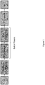
- Figure 1 illustrates an embodiment of the batch joining technique.
- standard front-end (FE) processing such as etching, grinding, polishing, structuring and/or metal deposition to for source, gate and drain contacts may be performed (Block 100) and one or more thin solder preforms cut and placed on a metal region of one or more semiconductor dies and/or on a metal region of one or more substrates (Block 110).
- Each thin solder preform can be stamped or cut from a reel of preform solder material as part of the batch joining technique, or can be a pre-cut preform, a pre-stamped preform, etc.
- Each thin solder preform may be applied during die assembly or may be pre-applied to the substrate(s) or a semiconductor wafer.
- a thin solder preform is applied to a front side or a back side of a semiconductor wafer which includes a plurality of semiconductor dies.
- the semiconductor dies are singulated, e.g., by sawing, laser cutting, etching, etc.
- the thin solder preform may instead be applied after the die singulation process.
- the semiconductor dies to be soldered using a thin solder preform may be heated and a thin solder preform may be applied to a front side or a back side of each heated semiconductor die.
- the thin solder preform may be stamped with the corresponding semiconductor die.
- the thin solder preform may be applied by roll cladding, pre-melting, printing and re-casting, etc.
- Each thin solder preform used as part of the batch joining technique may be cut by stamping, laser cutting, etching, etc.
- Thin solder preforms processed at the same time may have the same or different thicknesses depending on the types of semiconductor dies and substrates to be joined. More than one thin solder preform may be applied to the same or different substrate as part of the batch joining technique.
- the batch joining technique may be carried out free of flux, as the die attach process may be done in a vacuum environment under reducing atmosphere and with formic acid.
- This is also valid for printed thin solder preforms, where the paste may be free of flux, as the surfaces may be cleaned with formic acid during the batch joining technique.
- all semiconductor dies to be soldered at the same time may be joined to the same substrate, joined to individual substrates, or joined in respective groups to separate substrates via the batch joining technique.
- each thin solder preform is a formed of solder that is thin and extremely uniform, e.g., such as a thin metal film or foil, and has a maximum thickness of 30 ⁇ m (microns), e.g., a maximum thickness of 15 ⁇ m, e.g., a maximum thickness of 10 ⁇ m or even thinner.
- Some semiconductor dies may be attached to the substrate using a thicker solder preform having a maximum thickness greater than 30 ⁇ m or using a solder paste.
- Connectors such as pins, rivets, metal plates, etc. also may be attached to the substrate using a thicker solder preform having a maximum thickness greater than 30 ⁇ m or using a solder paste.
- the term 'thin solder preform' as used herein means a solder preform having a maximum thickness of 30 ⁇ m and a lower melting point than the metal region of each semiconductor die and each metal region of the substrate to be joined by the thin solder preform.
- Such a thin solder preform fully reacts with the die backside metal and the substrate material during the diffusion soldering process, and the resulting soldered joint (bond line) formed between the semiconductor die and substrate has a high melting phase throughout the entire soldered joint.
- the term 'high melting phase' as used herein means an intermetallic phase having a melting point above the melting point of the preform and above the soldering temperature of the diffusion soldering process.
- a soldered joint without a high melting phase throughout the entire soldered joint may be suitable for some types of semiconductor dies and connectors, and hence all dies and devices processed at the same time as part of the batch joining technique are not necessarily attached to the substrate using a thin solder preform.
- Some semiconductor dies and/or connectors may be attached to the substrate using a thicker solder preform having a maximum thickness greater than 30 ⁇ m or using a solder paste.
- all semiconductor dies processed at the same time as part of the batch joining technique may be attached to the substrate using a thin solder preform.
- the batch joining technique illustrated in Figure 1 also includes picking and placing each semiconductor die to be processed at the same time on a corresponding substrate (Block 120). As described above, all semiconductor dies to be processed at the same time via the batch joining technique may be placed on the same substrate, placed on individual substrates, or placed on respective groups of separate substrates. Connectors such as pins, rivets, metal plates, etc. also may be attached to the substrate(s) using a thicker solder preform having a maximum thickness greater than 30 ⁇ m or using a solder paste, via the batch joining technique.
- the batch joining technique illustrated in Figure 1 also includes a batch die soldering process (Block 130).
- the batch die soldering process involves soldering each semiconductor die to the same or different metal region of a substrate. If the electronic device being produced includes connectors such as pins, rivets, metal plates, etc., the connectors may be attached to the substrate as part of the die soldering process.
- the die soldering process involves soldering each component (semiconductor dies and connectors if applicable) to the same or different metal region of a substrate without applying (mechanical) pressure directly to the components. This way, different types of semiconductor dies, die attach materials and connectors may be processed at the same time via the batch joining technique without having to accommodate different height tolerances.
- the corresponding soldered joint is formed by diffusion soldering without applying (mechanical) pressure directly to the semiconductor die.
- the soldering temperature of the diffusion soldering process may be set so that the solder preform melts and fully reacts with the metal region of the corresponding semiconductor die and a metal region of the substrate to form one or more intermetallic phases throughout the entire soldered joint.
- Each intermetallic phase has a melting point above the melting point of the preform and the soldering temperature of the die soldering process.
- multiple dies and connectors may be soldered at the same time without concern for different thicknesses of the dies, substrates, connectors and/or die attach materials.
- some semiconductor dies may be soldered using thin solder preforms
- other semiconductor dies may be soldered using thicker solder preforms
- still other semiconductor dies and/or connectors may be soldered using solder paste.
- solder paste For each semiconductor die soldered using a thin solder preform, if the metal region of the semiconductor die and the metal region of the substrate comprise the same metal or metal alloy, a single intermetallic phase is formed throughout the entire soldered joint by the diffusion soldering process.
- the joining technique illustrated in Figure 1 may also include standard front side (FS) contact formation processing (Block 140), which may include forming electrically conductive structures for source and gate contacts and a solderable front side metallization and standard back-end (BE) processing (Block 150), which may include depositing a metallic layer stack for electrically connecting the drain contact.
- FS front side
- BE solderable front side metallization
- BE standard back-end
- the front side contact formation processing and standard back-end processing may be performed using the same or different equipment, lines and/or sites as the batch die soldering process represented by Blocks 110 through 130.
- a first soldered joint may be formed between a metal region of a first semiconductor die and a first metal region of a substrate using a first solder preform via the batch die soldering process (Block 130) and without applying (mechanical) pressure directly to the first semiconductor die.
- the first solder preform has a maximum thickness of 30 ⁇ m and a lower melting point than both the metal region of the first semiconductor die and the first metal region of the substrate.
- a soldering temperature of the soldering process may be set so that the first solder preform melts and fully reacts with the metal region of the first semiconductor die and the first metal region of the substrate to form one or more intermetallic phases throughout the entire first soldered joint.
- Each intermetallic phase has a melting point above the melting point of the preform and the soldering temperature.
- a second semiconductor die may be soldered to the first or different metal region of the substrate via the batch die soldering process (Block 130) used to form the first soldered joint and without applying pressure directly to the second semiconductor die. Additional semiconductor dies and/or connectors such as pins, rivets, metal plates, etc. also may be attached to the substrate via the batch die soldering process (Block 130) used to solder the first and second semiconductor dies.
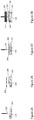
- Figures 2A through 2D illustrate an embodiment of Blocks 110 through 130 of the method shown in Figure 1 . While Figures 2A through 2D show a first semiconductor die 200 being joined to a first substrate 202 by diffusion soldering using a first thin solder preform 204, more than one semiconductor die is soldered at the same time to the same substrate, joined to individual substrates, or joined in respective groups to separate substrates as part of the batch joining technique, as previously explained herein.
- the diffusion soldering process shown in Figures 2A through 2D may be applied to each component being soldered via the batch joining technique using a solder preform.
- Figure 2A shows a first liquid 206 being applied to the first substrate 202.
- the first liquid 206 is a volatile, non-reactive liquid which keeps the first thin solder preform 204 in place on the first substrate 202 by surface tension.
- the first substrate 202 is a leadframe or a metal clip having a metal die attach region 208 to which the first semiconductor die 200 is to be joined.
- the leadframe or metal clip may comprise Cu, Ni and/or Ag, for example.
- the first substrate 202 comprises a ceramic and a metal layer attached to the ceramic and to which the first semiconductor die 200 is to be joined.
- the metal layer comprises and/or is plated with Cu, Ni, Ag, Au, Pd, Pt, NiV, NiP, NiNiP, NiP/Pd, Ni/Au, NiP/Pd/Au, or NiP/Pd/AuAg. Still other types of metals/metal alloys and substrates may be used.
- Figure 2B shows the first thin solder preform 204 during placement on the first substrate 202 with the first liquid 206.
- the first liquid 206 maintains the position of the first thin solder preform 204 relative to the first substrate 202 by surface tension.
- the first thin solder preform 204 comprises Sn, Zn, In, Ga, Bi, Cd or any alloy thereof.
- the first thin solder preform 204 may comprise Sn/Ag/Cu, Sn/Ag, Sn/Ag/Sb, Sn/Sb, Sn/Cu or Au80/Sn20. Still other types of thin solder preforms may be used.
- the first thin solder preform 204 may be applied to the first semiconductor die 200 instead of the first substrate 202. In this case, the first substrate 202 in Figure 2B instead would be the first semiconductor die 200 or a semiconductor wafer from which the first die 200 is produced.
- the first thin solder preform 204 may be applied to a front side or a back side of a semiconductor wafer which includes the first semiconductor die 200 and a plurality of additional semiconductor dies, or may be applied to the front side or back side of the first semiconductor die 200 after the die singulation process, both as previously described herein.
- Figure 2C shows a second liquid 210 being applied to the first thin solder preform 204.
- the second liquid 210 is a volatile, non-reactive liquid which keeps the first semiconductor die 200 in place on the first thin solder preform 204 by surface tension.
- the first and second liquids 206, 210 may be the same or different type of liquid.
- Figure 2D shows the first semiconductor die 200 during placement on the first thin solder preform 204 with the second liquid 210.
- the second liquid 210 maintains the position of the first semiconductor die 200 relative to the first thin solder preform 204 by surface tension.
- a clamping mechanism (not shown) may be used to handle the first thin solder preform 204, to transport the assembly to a diffusion soldering oven.
- a soldered joint is then formed between a metal region 212 of the first semiconductor die 200 facing the first substrate 202 and a metal region 208 of the first substrate 202 via a diffusion soldering process and without applying (mechanical) pressure directly to the first semiconductor die 200.
- the metal region 212 of the first semiconductor die 200 may be a metal layer applied to the back side or front side of the first semiconductor die 200.
- the metal region 212 of the first semiconductor die 200 comprises and/or is plated with Cu, Ni, Ag, Au, Pd, Pt, NiV, NiP, NiNiP, NiP/Pd, Ni/Au, NiP/Pd/Au, NiP/Pd/AuAg, NiV/Ag, NiV/Au, or NiSi/Ag.
- the metal region 212 may be a terminal of the first semiconductor die 200, e.g., a load or control terminal in the case of a power transistor die such as a power MOSFET (metal-oxide semiconductor field-effect transistor), IGBT (insulated gate bipolar transistor), HEMT (high electron mobility transistor), etc., a control or I/O (input/output) terminal in the case of a logic die such as a gate driver, microcontroller, memory, etc., a terminal of a passive die such as an inductor or capacitor die, etc.
- a power transistor die such as a power MOSFET (metal-oxide semiconductor field-effect transistor), IGBT (insulated gate bipolar transistor), HEMT (high electron mobility transistor), etc.
- a control or I/O (input/output) terminal in the case of a logic die such as a gate driver, microcontroller, memory, etc.
- a terminal of a passive die such as an inductor or capacitor die, etc.
- the metal region 212 of the first semiconductor die 200 and the metal region 208 of the first substrate 202 to be joined together by diffusion soldering process and the first thin solder preform 204 may comprise the same or different metal/metal alloy. If the metal regions 212, 208 joined by the first thin solder preform 204 comprise the same metal or metal alloy as the first thin solder preform 204, a single intermetallic phase is formed throughout the entire soldered joint formed between the first die 200 and first substrate 202, as previously explained herein.
- the metal region 212 of the first semiconductor die 200 and the metal region 208 of the first substrate 202 to be joined both comprise Cu or the same Cu-rich alloy
- Cu will dissolve via the liquified preform material during the diffusion soldering process until a certain concentration is reached, at which point the joint solidifies.
- the resulting Cu-based intermetallic phase will not melt again at the solder temperature of the diffusion soldering process.
- other types of common die and substrate metallization such as Ni-rich and Ag-rich alloys, for example.
- the metal region 212 of the first semiconductor die 200 and the metal region 208 of the first substrate 202 comprise a different metal/metal alloy, a plurality of intermetallic phases are formed throughout the entire soldered joint.
- the first thin solder preform 204 fully reacts with the die metal 212 and the substrate metal 208 during the diffusion solder process so that the soldered joint formed between the first die 200 and first substrate 202 has a high melting phase throughout the entire soldered joint.
- Figure 3 illustrates an embodiment of the batch joining technique represented by Blocks 110 through 130 in Figure 1 .
- Figure 3 shows first and second semiconductor dies 200', 200" being joined to a metal region 208 of a substrate 202 by the same soldering process.
- the first and second semiconductor dies 200', 200" are both power semiconductor dies.
- the first semiconductor die 200' is a power semiconductor die such as a power MOSFET, IGBT, HEMT, etc.
- the second semiconductor die 200" is a passive semiconductor die such as an inductor or capacitor die, etc., or a logic semiconductor die such as a gate driver, microcontroller, memory, etc.
- the second semiconductor die 200" is soldered to the substrate 202 using the same thin solder preform 204 used to join the first semiconductor die 200" to the substrate 202.
- both the first semiconductor die 200' and the second semiconductor die 200" are joined to the substrate 202 by a respective soldered joint having one or more intermetallic phases present throughout the entire soldered joint.
- Formic acid 302 may be introduced into the vacuum oven 300 as part of the batch die soldering process (Block 130).
- the formic acid 302 removes oxidation from the substrate 202, each die metallization 212', 212" and the thin solder preform 204, thereby increasing wettability of each die metallization 212', 212" and the substrate metallization 208 and completely filling the space between the dies 200', 200" and substrate 202.
- the temperature of the vacuum oven 300 is increased under vacuum conditions to the soldering temperature for a duration over which the thin solder preform 204 melts and fully reacts with the corresponding die metallization 212', 212" and the substrate metallization 208 to form one or more intermetallic phases throughout the corresponding entire soldered joint.
- the batch die soldering process is performed without applying (mechanical) pressure directly to the semiconductor dies 200', 200". With this approach, standard diffusion soldering equipment may be used without redesign.
- soldered joint does not exceed the lateral (length and width) dimensions of the semiconductor dies 200', 200", and has the same length-to-width aspect ratio as the semiconductor dies 200', 200".
- the respective die metallization 212', 212" and the substrate metallization 208 may comprise the same metal or metal alloy so that a single intermetallic phase is present throughout the corresponding entire soldered joint.
- Figure 4 illustrates another embodiment of the batch joining technique represented by Blocks 110 through 130 in Figure 1 .
- the embodiment illustrated in Figure 4 is similar to the embodiment illustrated in Figure 3 .
- the first and second semiconductor dies 200', 200" are being joined to different metal regions 208', 208" of the substrate 202 by the same soldering process.
- the first and second semiconductor dies 200', 200" may be soldered to different metal regions 208', 208" of the substrate 202 by separate thin solder preforms 204', 204".
- the soldering temperature of the soldering process may be set so that the thin solder preform 204" used to form the second soldered joint melts and fully reacts with the metal region 212" of the second semiconductor die 200" and the corresponding metal region 208" of the substrate 202 during the soldering process, to form one or more intermetallic phases throughout the entire soldered joint between the second die 200" and the substrate 202.
- the second semiconductor die 200" may instead be soldered to the substrate 202 using a thicker solder preform having a maximum thickness greater than 30 ⁇ m.
- a high melting phase is not producible throughout the entire soldered joint in a reasonable amount of time and the resulting soldered joint between the second die 200" and the substrate 202 is devoid of intermetallic phases in a middle part of the soldered joint.
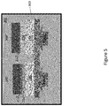
- Figure 5 illustrates another embodiment of the batch joining technique represented by Blocks 110 through 130 in Figure 1 .
- the embodiment illustrated in Figure 5 is similar to the embodiment illustrated in Figure 4 .
- the second semiconductor die 200" is soldered to the substrate 202 using a solder paste 304 instead of a solder preform.
- the solder paste 304 may be applied to the metal region 212" of the second semiconductor die 200" and/or to the corresponding metal region 308" of the substrate 202.
- the solder paste 304 is then reflowed to form a second soldered joint between the metal region 212" of the second semiconductor die 200" and the corresponding metal region 308" of the substrate 202, without applying (mechanical) pressure directly to the second semiconductor die 200".
- the solder paste 304 may be reflowed at the same time that the soldered joint is formed between the first semiconductor die 200' and the substrate 202. If the soldered joint between the first semiconductor die 200' and the substrate 202 has a melting point above a reflow temperature of the solder paste 304, the solder paste 304 may instead be reflowed after the soldered joint is formed between the first semiconductor die 200' and the substrate 202 so that the soldered joint between the first semiconductor die 200' and the substrate 202 does not melt during reflowing of the solder paste 304.
- Figure 5 shows the second semiconductor die 200" soldered to a different metal region 308" of the substrate 202 than the first semiconductor die 200'. The second semiconductor die 200" may instead be soldered to the same metal region 308' of the substrate 202 as the first semiconductor die 200'.
- the embodiment illustrated in Figure 5 combines diffusion soldering with standard soldering, e.g., by using a thin solder preform 204' to achieve a diffusion soldered joint and using a solder paste 304 or a thicker solder preform to achieve a standard soldered joint.
- Such an approach may be beneficial for yield purposes.
- diffusion soldered joints may be used for devices having a high lifetime reliability requirement and standard soldered joints may be used for devices having a lower lifetime reliability requirement.
- Passive devices and low power devices may also use standard soldering, and high power and high reliability devices may use diffusion soldering.
- the first and second semiconductor dies 200', 200" are batch soldered to a substrate 200 without applying (mechanical) pressure directly to either semiconductor die 200' 200". More than two semiconductor dies 200 may be joined to the substrate 202 via the batch joining technique, and additional components such as connectors like pins, rivets, metal plates, etc. also may be attached to the substrate 202 using a thin solder preform, a thicker solder preform having a maximum thickness greater than 30 ⁇ m or a solder paste as part of the batch joining technique.
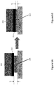
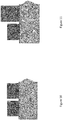
- Figures 6A and 6B illustrate another embodiment of Blocks 110 through 130 of the method shown in Figure 1 .
- the thin solder preform 204 used to join the metal region 212 of a semiconductor die 200 to the metal region 208 of a substrate 202 has a smaller width and/or a smaller length (W/L) than the metal region 212 of the die 200 prior to the batch soldering process, as shown in Figure 5A.
- the thin solder preform 204 melts and spreads over the entire metal region 212 of the semiconductor die 200 during the batch soldering process, so that the resulting soldered joint 400 has a thickness (T2) which is less than the initial maximum thickness (T1) of the solder preform 204, as shown in Figure 6B .
- T2 thickness
- T1 initial maximum thickness
- a thin solder preform 204 may be chosen smaller than lateral dimensions of the semiconductor die 200, e.g., as illustrated in Figures 6A and 6B , to enable narrow design rule / low clearance.
- the use of formic acid 302 as part of the batch soldering process provides excellent wetting of thin solder preforms 204 to a substrate 202, completely filling space between the semiconductor dies 200 and the substrate 202.
- the type of solder preform / material may be exchanged easily without requiring modifications to the joining / diffusion soldering process.
- Figure 7 shows an embodiment of an electronic device in which first and second semiconductor dies 200', 200" are soldered to the same substrate 202 using separate solder preforms 204', 204".
- the semiconductor dies 200', 200" are joined to the same metal region 208 of the substrate 202 via respective soldered joints formed between the metal region (out of view) of the corresponding semiconductor die 200', 200" and the metal region 208 of the substrate 202.
- At least one of the solder preforms 204', 204" is a thin preform so that the corresponding soldered joint has one or more intermetallic phases throughout the entire soldered joint.
- the first semiconductor die 200' is a power semiconductor die such as a power MOSFET, IGBT, HEMT, etc.
- the second semiconductor die 200" is a passive semiconductor die such as an inductor or capacitor die, etc., or a logic semiconductor die such as a gate driver, microcontroller, memory, etc.
- Figure 8 shows an embodiment of an electronic device in which the substrate 202 has a plurality of metal regions 208 separated from one another.
- the substrate 202 may comprise a ceramic 500 and a metal layer 502 attached to the ceramic 500 and into which the plurality of separated metal regions 208 is patterned.
- the metal layer 502 comprises and/or is plated with Cu, Ni, Ag, Au, Pd, Pt, NiV, NiP, NiNiP, NiP/Pd, Ni/Au, NiP/Pd/Au, or NiP/Pd/AuAg. Still other types of metals/metal alloys and substrates may be used.
- a first thin solder preform 204' is applied to a first metal region 208' of the substrate 202.
- a plurality of first semiconductor dies 200' is soldered to the first metal region 208' of the substrate 202.
- a soldered joint (out of view) is formed between a metal region (out of view) of each first semiconductor die 200' and the first metal region 208' of the substrate 202 using the first thin solder preform 204' via a diffusion soldering process which does not apply pressure (mechanical) directly to the first semiconductor dies 200'.
- the first thin solder preform 204' has a maximum thickness of 30 ⁇ m and a lower melting point than both the metal region of the first semiconductor dies 200' and the first metal region 208' of the substrate 202.
- a second thin solder preform 204" is applied to a second metal region 208" of the substrate 202.
- a plurality of second semiconductor dies 200" is soldered to the second metal region 208" of the substrate 202.
- a soldered joint (out of view) is formed between a metal region (out of view) of each second semiconductor die 200" and the second metal region 208" of the substrate 202 using the second thin solder preform 204" via the diffusion soldering process used to solder the plurality of first semiconductor dies 200' to the first metal region 208' of the substrate 202, without applying (mechanical) pressure directly to the second semiconductor dies 200".
- the second thin solder preform 204" has a maximum thickness of 30 ⁇ m and a lower melting point than both the metal region of the second semiconductor dies 200" and the second metal region 208" of the substrate 202.
- the first solder preform 204' or the second solder preform 204" may instead be thicker than the other solder preform so that the corresponding soldered joint formed by the thicker solder preform is devoid of intermetallic phases in a middle part of that soldered joint.
- a high melting phase is not producible throughout the entire soldered joint formed from the thicker solder preform in a reasonable amount of time, and thus the middle part of the resulting soldered joint will not be converted to an intermetallic compound and will instead remain at the original melting temperature.
- Figure 9 shows another embodiment of an electronic device in which the substrate 202 has a plurality of metal regions 208 separated from one another.
- the embodiment illustrated in Figure 9 is similar to the embodiment illustrated in Figure 8 .
- the electronic device also includes one or more connectors 600 such as pins, rivets, metal plates, etc. soldered to the substrate 202 via the batch joining technique described herein, without applying (mechanical) pressure directly to the connector(s) 600.
- Each connector 600 may be soldered to the substrate 202 by forming a soldered joint (out of view) between the respective connector 600 and the same or different metal region(s) 208 of the substrate 202 to which the semiconductor dies 200 are soldered.
- each connector 600 is soldered to the substrate 202 using the same solder preform as one or more of the semiconductor dies 200 or using a different solder preform, via the same soldering process used to form the soldered joints between the semiconductor dies 200 and the substrate 202 and without applying (mechanical) pressure directly to the connectors 600.
- the solder preform has a maximum thickness of 30 ⁇ m, a high melting phase results throughout the entire soldered joint formed between the connectors 600 and the substrate 202. If the solder preform is thicker than 30 ⁇ m, a high melting phase does not result throughout the entire soldered joint and the middle part of the soldered joint is not converted to an intermetallic compound but instead remains at the original melting temperature of the solder preform.
- each connector 600 is soldered to the substrate 202 by applying a solder paste (not shown) to the connector 600 and/or to the metal region 208 of the substrate 202 to which the connector 600 is to be joined.
- the solder paste is then reflowed to form a soldered joint between each connector 600 and the corresponding metal region 208 of the substrate 202, without applying (mechanical) pressure directly to the connectors 600.
- Figure 11 shows another embodiment of an electronic device produced in accordance with the batch joining technique described herein.
- the embodiment illustrated in Figure 11 is similar to the embodiment illustrated in Figure 10 .
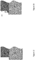
- the first and second semiconductor dies 200', 200" have different heights (Td1 ⁇ Td2). Since the batch joining technique described herein does not apply (mechanical) pressure directly to the components being soldered, semiconductor dies 200', 200" of different heights Td1, Td2 may be processed at the same time without requiring additional equipment for accommodating different height tolerances.
- Figure 12 shows another embodiment of an electronic device produced in accordance with the batch joining technique described herein.
- the soldered joint 700 between the semiconductor die 200 and the substrate 202 is formed from a thin solder preform and therefore has one or more intermetallic phases throughout the entire soldered joint 700.
- the soldered joint 700 has the same lateral dimensions (length and width) as the semiconductor die 200 which is joined to the substrate 202 by the soldered joint 700.
- Figure 13 shows another embodiment of an electronic device produced in accordance with the batch joining technique described herein.
- the embodiment illustrated in Figure 13 is similar to the embodiment illustrated in Figure 12 .
- the soldered joint laterally extends ('ext') beyond one or more side faces 800 of the semiconductor die 200.
- the semiconductor die 200 has a smaller footprint than the solder preform used to form the soldered joint between the die 200 and the substrate 202.
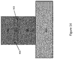
- Figure 14 shows another embodiment of an electronic device produced in accordance with the batch joining technique described herein.
- a first semiconductor die 200 is soldered to a substrate 202 via a first soldered joint 700 and the first soldered joint 700 has one or more intermetallic phases throughout the entire soldered joint 700, each intermetallic phase formed from a solder preform diffused into a metal region of the first semiconductor die 200 and a metal region of the substrate 202.
- an additional semiconductor die 900 is soldered to a side 902 of the first semiconductor die 200 facing away from the substrate 202 without applying (mechanical) pressure directly to the additional semiconductor die 900.
- the soldered joint 904 between the first semiconductor die 200 and the additional semiconductor die 900 may be formed from a solder preform or solder paste.
- the soldered joint 904 between the first semiconductor die 200 and the additional semiconductor die 900 has one or more intermetallic phases. If the solder preform has a maximum thickness of 30 ⁇ m, the soldered joint 904 has one or more intermetallic phases throughout the entire first soldered joint 904. Otherwise, the soldered joint 904 is devoid of intermetallic phases in a middle part of the soldered joint 904.
- the soldered joint 904 formed between the first semiconductor die 200 and the additional semiconductor die 900 may be formed by applying a solder paste to a metal region at the side 906 of the additional semiconductor die 900 facing the substrate 202 and/or to a metal region at the side 902 of the first semiconductor die 200 facing away from the substrate 202. The solder paste is then reflowed to form the soldered joint 904 between the first semiconductor die 900 and the additional semiconductor die 200, without applying (mechanical) pressure directly to the additional semiconductor die 900.
- Figure 15 shows another embodiment of an electronic device produced in accordance with the batch joining technique described herein.
- the embodiment illustrated in Figure 15 is similar to the embodiment illustrated in Figure 14 .
- the additional component soldered to the top side 902 of the first semiconductor 200 is a metal clip 1000 instead of an additional semiconductor die 900.
- the opposite end of the metal clip 1000 may be soldered to the same substrate 202 as the first semiconductor die 200 or to a different substrate (not shown) such as a PCB (printed circuit board).
- the soldered joint 904 between the first semiconductor die 200 and the metal clip 1000 may be formed from a solder preform or solder paste.
- the soldered joint 904 between the first semiconductor die 200 and the metal clip 1000 has one or more intermetallic phases. If the solder preform has a maximum thickness of 30 ⁇ m, the soldered joint 904 has one or more intermetallic phases throughout the entire first soldered joint 904. Otherwise, the soldered joint 904 is devoid of intermetallic phases in a middle part of the soldered joint 904.
- the soldered joint 904 formed between the first semiconductor die 200 and the metal clip 1000 may be formed by applying a solder paste to the side 1002 of the metal clip 1000 facing the substrate 202 and/or to a metal region at the side 902 of the first semiconductor die 200 facing away from the substrate 202. The solder paste is then reflowed to form the soldered joint 904 between the metal clip 1000 and the first semiconductor die 200, without applying (mechanical) pressure directly to the metal clip 1000.
Landscapes
- Engineering & Computer Science (AREA)
- Mechanical Engineering (AREA)
- Chemical & Material Sciences (AREA)
- Materials Engineering (AREA)
- Electric Connection Of Electric Components To Printed Circuits (AREA)
- Die Bonding (AREA)
Abstract
Description
- Thermal and electrical performance play an increasing role in the advancement of semiconductor technologies. These factors, coupled with miniaturization and increased performance, demand a high-performance die (chip) attach process and material. Diffusion soldering is one such die attach process.
- Diffusion soldering involves sputtering a thin layer of solder material onto the backside of a semiconductor wafer. The deposition of the solder material represents a significant fraction of the overall wafer cost. In addition, a high force is used during the die attach process to achieve a form-fit interconnect, as the sputtered solder layer is thin and the lead frame to which the devices are attached has a defined curvature.
- The diffusion soldering process described above also requires specialized equipment, including a bond force unit for applying the high force to the devices to achieve a form-fit interconnect. Furthermore, mechanical pressure is applied individually to each die and must be maintained until a significant portion of the solder has solidified isothermally, limiting the throughput of the die attach process. In addition, the soldering temperature must be high to enable a full reaction and isothermal solidification in a short time.
- Thus, there is a need for an improved batch diffusion soldering process.
- According to an embodiment of a method of batch soldering, the method comprises: forming a first soldered joint between a metal region of a first semiconductor die and a first metal region of a substrate using a first solder preform via a soldering process which does not apply pressure directly to the first semiconductor die, the first solder preform having a maximum thickness of 30 µm and a lower melting point than both the metal region of the first semiconductor die and the first metal region of the substrate; setting a soldering temperature of the soldering process so that the first solder preform melts and fully reacts with the metal region of the first semiconductor die and the first metal region of the substrate to form one or more intermetallic phases throughout the entire first soldered joint, each of the one or more intermetallic phases having a melting point above the melting point of the preform and the soldering temperature; and soldering a second semiconductor die to the first or different metal region of the substrate, without applying pressure directly to the second semiconductor die.
- The second semiconductor die may be soldered to the substrate via the same or different soldering process used to form the first soldered joint.
- Separately or in combination, soldering the second semiconductor die to the substrate may comprise forming a second soldered joint between a metal region of the second semiconductor die and the first or different metal region of the substrate using the first solder preform or a second solder preform, via the same soldering process used to form the first soldered joint and without applying pressure directly to the second semiconductor die.
- Separately or in combination, the soldering temperature of the soldering process may be set so that the solder preform used to form the second soldered joint melts and fully reacts with the metal region of the second semiconductor die and the first or different metal region of the substrate during the soldering process, to form one or more intermetallic phases throughout the entire second soldered joint.
- Separately or in combination, the second soldered joint may be formed using the second solder preform, the second solder preform may be thicker than the first solder preform, and the second soldered joint may be devoid of intermetallic phases in a middle part of the second soldered joint.
- Separately or in combination, the second soldered joint may be formed using the second solder preform, and the second soldered joint may be between the metal region of the second semiconductor die and the first metal region of the substrate.
- Separately or in combination, soldering the second semiconductor die to the substrate may comprise: applying a solder paste to a metal region of the second semiconductor die and/or to the first or different metal region of the substrate; and reflowing the solder paste to form a second soldered joint between the metal region of the second semiconductor die and the first or different metal region of the substrate, without applying pressure directly to the second semiconductor die.
- Separately or in combination, the solder paste may be reflowed at the same time that the first soldered joint is formed.
- Separately or in combination, the solder paste may be reflowed after the first soldered joint is formed, and the first soldered joint may have a melting point above a reflow temperature of the solder paste so that the first soldered joint does not melt during reflowing of the solder paste.
- Separately or in combination, the method may further comprise soldering a connector to the substrate, without applying pressure directly to the connector.
- Separately or in combination, soldering the connector to the substrate may comprise forming a soldered joint between the connector and the first or different metal region of the substrate using the first solder preform or a second solder preform, via the same soldering process used to form the first soldered joint and without applying pressure directly to the connector.
- Separately or in combination, soldering the connector to the substrate may comprise: applying a solder paste to the connector and/or to the first or different metal region of the substrate; and reflowing the solder paste to form a soldered joint between the connector and the first or different metal region of the substrate, without applying pressure directly to the connector.
- Separately or in combination, the method may further comprise soldering a third semiconductor die to a side of the first or the second semiconductor die facing away from the substrate, without applying pressure directly to the third semiconductor die.
- Separately or in combination, soldering the third semiconductor die to the side of the first or the second semiconductor die facing away from the substrate may comprise forming a soldered joint between a metal region of the third semiconductor die facing the substrate and a metal region of the first or the second semiconductor die facing away from the substrate using an additional solder preform, and without applying pressure directly to the third semiconductor die.
- Separately or in combination, soldering the third semiconductor die to the side of the first or the second semiconductor die facing away from the substrate may comprise: applying a solder paste to a metal region of the third semiconductor die facing the substrate and/or to a metal region of the first or the second semiconductor die facing away from the substrate; and reflowing the solder paste to form a soldered joint between the third semiconductor die and the first or the second semiconductor die, without applying pressure directly to the third semiconductor die.
- Separately or in combination, the method may further comprise soldering a metal clip to a side of the first or the second semiconductor die facing away from the substrate, without applying pressure directly to the metal clip.
- Separately or in combination, soldering the metal clip to the side of the first or the second semiconductor die facing away from the substrate may comprise forming a soldered joint between the metal clip and a metal region of the first or the second semiconductor die facing away from the substrate using an additional solder preform, and without applying pressure directly to the metal clip.
- Separately or in combination, soldering the metal clip to the side of the first or the second semiconductor die facing away from the substrate may comprise: applying a solder paste to the metal clip and/or to a metal region of the first or the second semiconductor die facing away from the substrate; and reflowing the solder paste to form a soldered joint between the metal clip and the first or the second semiconductor die, without applying pressure directly to the metal clip.
- According to an embodiment of an electronic device, the electronic device comprises: a first semiconductor die having a metal region; a substrate having a plurality of metal regions; a first soldered joint between the metal region of the first semiconductor die and a first metal region of the substrate, the first soldered joint having one or more intermetallic phases throughout the entire soldered joint, each of the one or more intermetallic phases formed from a solder preform diffused into the metal region of the first semiconductor die and the first metal region of the substrate; and a second semiconductor die soldered to the first or different metal region of the substrate.
- A second soldered joint may be formed between a metal region of the second semiconductor die and the first or different metal region of the substrate. The second soldered joint may have one or more intermetallic phases throughout the entire second soldered joint or may be devoid of intermetallic phases in a middle part of the second soldered joint. A reflowed solder paste may form the second soldered joint.
- Separately or in combination, the first semiconductor die may be a power semiconductor die and the second semiconductor die may be a passive semiconductor die or a logic semiconductor die.
- Separately or in combination, the first semiconductor die may have a different thickness than the second semiconductor die.
- Separately or in combination, the first soldered joint may laterally extend beyond one or more side faces of the first semiconductor die.
- Separately or in combination, the electronic device may further comprise a connector attached to the first or different metal region of the substrate by a soldered joint having one or more intermetallic phases or a reflowed solder paste.
- Separately or in combination, the electronic device may further comprise a third semiconductor die attached to a side of the first or the second semiconductor die facing away from the substrate by a soldered joint having one or more intermetallic phases or a reflowed solder paste.
- Separately or in combination, the electronic device may further comprise a metal clip attached to a side of the first or the second semiconductor die facing away from the substrate by a soldered joint having one or more intermetallic phases or a reflowed solder paste.
- Those skilled in the art will recognize additional features and advantages upon reading the following detailed description, and upon viewing the accompanying drawings.
- The elements of the drawings are not necessarily to scale relative to each other. Like reference numerals designate corresponding similar parts. The features of the various illustrated embodiments can be combined unless they exclude each other. Embodiments are depicted in the drawings and are detailed in the description which follows.
-
Figure 1 illustrates a block diagram of an embodiment of a method of batch joining technique for semiconductor dies. -
Figures 2A through 2D illustrate respective cross-sectional views of an embodiment ofBlocks 110 through 130 of the method shown inFigure 1 . -
Figures 3 through 5 illustrate respective cross-sectional views of additional embodiments ofBlock 130 of the method shown inFigure 1 . -
Figures 6A and 6B illustrate respective cross-sectional views of another embodiment ofBlocks 110 through 130 of the method shown inFigure 1 . -
Figures 7 through 15 illustrate respective cross-sectional views of additional embodiments of electronic devices produced in accordance with the method shown inFigure 1 . - The embodiments described herein provide a batch joining process for producing electronic devices, whereby one or more semiconductor dies processed at the same time are soldered to the same or different substrate using a thin solder preform without applying (mechanical) pressure directly to the semiconductor dies. Each thin solder preform used in the batch joining process is thin enough, e.g., at most 30 µm thick, so that the soldering temperature of the diffusion soldering process may be set so that each thin solder preform melts and fully reacts with metal regions of the corresponding semiconductor die and substrate to form one or more intermetallic phases throughout the entire soldered joint. Since (mechanical) pressure is not directly applied to the semiconductor dies during the diffusion soldering process, multiple semiconductor dies may be processed at the same time via the batch joining process and different joining materials may be used to accommodate different (e.g. passive and/or active) device types.
-
Figure 1 illustrates an embodiment of the batch joining technique. According to this embodiment, standard front-end (FE) processing such as etching, grinding, polishing, structuring and/or metal deposition to for source, gate and drain contacts may be performed (Block 100) and one or more thin solder preforms cut and placed on a metal region of one or more semiconductor dies and/or on a metal region of one or more substrates (Block 110). Each thin solder preform can be stamped or cut from a reel of preform solder material as part of the batch joining technique, or can be a pre-cut preform, a pre-stamped preform, etc. - Each thin solder preform may be applied during die assembly or may be pre-applied to the substrate(s) or a semiconductor wafer. In one embodiment, a thin solder preform is applied to a front side or a back side of a semiconductor wafer which includes a plurality of semiconductor dies. After applying the thin solder preform to the semiconductor wafer, the semiconductor dies are singulated, e.g., by sawing, laser cutting, etching, etc. The thin solder preform may instead be applied after the die singulation process. For example, the semiconductor dies to be soldered using a thin solder preform may be heated and a thin solder preform may be applied to a front side or a back side of each heated semiconductor die. The thin solder preform may be stamped with the corresponding semiconductor die. In the case of pre-applying a thin solder preform to a substrate, the thin solder preform may be applied by roll cladding, pre-melting, printing and re-casting, etc. Each thin solder preform used as part of the batch joining technique may be cut by stamping, laser cutting, etching, etc. Thin solder preforms processed at the same time may have the same or different thicknesses depending on the types of semiconductor dies and substrates to be joined. More than one thin solder preform may be applied to the same or different substrate as part of the batch joining technique.
- In general, the batch joining technique may be carried out free of flux, as the die attach process may be done in a vacuum environment under reducing atmosphere and with formic acid. This is also valid for printed thin solder preforms, where the paste may be free of flux, as the surfaces may be cleaned with formic acid during the batch joining technique. In each case, all semiconductor dies to be soldered at the same time may be joined to the same substrate, joined to individual substrates, or joined in respective groups to separate substrates via the batch joining technique.
- For those semiconductor dies being attached to a substrate using a thin solder preform via diffusion soldering, each thin solder preform is a formed of solder that is thin and extremely uniform, e.g., such as a thin metal film or foil, and has a maximum thickness of 30 µm (microns), e.g., a maximum thickness of 15 µm, e.g., a maximum thickness of 10 µm or even thinner. Some semiconductor dies may be attached to the substrate using a thicker solder preform having a maximum thickness greater than 30 µm or using a solder paste. Connectors such as pins, rivets, metal plates, etc. also may be attached to the substrate using a thicker solder preform having a maximum thickness greater than 30 µ m or using a solder paste.
- In general, the term 'thin solder preform' as used herein means a solder preform having a maximum thickness of 30 µm and a lower melting point than the metal region of each semiconductor die and each metal region of the substrate to be joined by the thin solder preform. Such a thin solder preform fully reacts with the die backside metal and the substrate material during the diffusion soldering process, and the resulting soldered joint (bond line) formed between the semiconductor die and substrate has a high melting phase throughout the entire soldered joint. The term 'high melting phase' as used herein means an intermetallic phase having a melting point above the melting point of the preform and above the soldering temperature of the diffusion soldering process.
- At thicknesses above 30 µm and for soft solder pastes, a high melting phase is not producible throughout the entire soldered joint in a reasonable amount of time, and thus the middle part of the resulting soldered joint will not be converted to an intermetallic compound and will instead remain at the original melting temperature. A soldered joint without a high melting phase throughout the entire soldered joint may be suitable for some types of semiconductor dies and connectors, and hence all dies and devices processed at the same time as part of the batch joining technique are not necessarily attached to the substrate using a thin solder preform. Some semiconductor dies and/or connectors may be attached to the substrate using a thicker solder preform having a maximum thickness greater than 30 µm or using a solder paste. For some applications, all semiconductor dies processed at the same time as part of the batch joining technique may be attached to the substrate using a thin solder preform.
- The batch joining technique illustrated in
Figure 1 also includes picking and placing each semiconductor die to be processed at the same time on a corresponding substrate (Block 120). As described above, all semiconductor dies to be processed at the same time via the batch joining technique may be placed on the same substrate, placed on individual substrates, or placed on respective groups of separate substrates. Connectors such as pins, rivets, metal plates, etc. also may be attached to the substrate(s) using a thicker solder preform having a maximum thickness greater than 30 µm or using a solder paste, via the batch joining technique. - The batch joining technique illustrated in
Figure 1 also includes a batch die soldering process (Block 130). The batch die soldering process involves soldering each semiconductor die to the same or different metal region of a substrate. If the electronic device being produced includes connectors such as pins, rivets, metal plates, etc., the connectors may be attached to the substrate as part of the die soldering process. The die soldering process involves soldering each component (semiconductor dies and connectors if applicable) to the same or different metal region of a substrate without applying (mechanical) pressure directly to the components. This way, different types of semiconductor dies, die attach materials and connectors may be processed at the same time via the batch joining technique without having to accommodate different height tolerances. - For each semiconductor die being joined to a substrate by a thin solder preform, the corresponding soldered joint is formed by diffusion soldering without applying (mechanical) pressure directly to the semiconductor die. By using a thin solder preform that is at most 30 µm thick, the soldering temperature of the diffusion soldering process may be set so that the solder preform melts and fully reacts with the metal region of the corresponding semiconductor die and a metal region of the substrate to form one or more intermetallic phases throughout the entire soldered joint. Each intermetallic phase has a melting point above the melting point of the preform and the soldering temperature of the die soldering process.
- By not applying direct pressure to the semiconductor dies and connectors as part of the soldering process, multiple dies and connectors may be soldered at the same time without concern for different thicknesses of the dies, substrates, connectors and/or die attach materials. This way, some semiconductor dies may be soldered using thin solder preforms, other semiconductor dies may be soldered using thicker solder preforms, and still other semiconductor dies and/or connectors may be soldered using solder paste. For each semiconductor die soldered using a thin solder preform, if the metal region of the semiconductor die and the metal region of the substrate comprise the same metal or metal alloy, a single intermetallic phase is formed throughout the entire soldered joint by the diffusion soldering process.
- The joining technique illustrated in
Figure 1 may also include standard front side (FS) contact formation processing (Block 140), which may include forming electrically conductive structures for source and gate contacts and a solderable front side metallization and standard back-end (BE) processing (Block 150), which may include depositing a metallic layer stack for electrically connecting the drain contact. The front side contact formation processing and standard back-end processing may be performed using the same or different equipment, lines and/or sites as the batch die soldering process represented byBlocks 110 through 130. - In accordance with the batch joining technique illustrated in
Figure 1 , a first soldered joint may be formed between a metal region of a first semiconductor die and a first metal region of a substrate using a first solder preform via the batch die soldering process (Block 130) and without applying (mechanical) pressure directly to the first semiconductor die. The first solder preform has a maximum thickness of 30 µm and a lower melting point than both the metal region of the first semiconductor die and the first metal region of the substrate. Further in accordance with the batch joining technique illustrated inFigure 1 , a soldering temperature of the soldering process may be set so that the first solder preform melts and fully reacts with the metal region of the first semiconductor die and the first metal region of the substrate to form one or more intermetallic phases throughout the entire first soldered joint. Each intermetallic phase has a melting point above the melting point of the preform and the soldering temperature. Further in accordance with the batch joining technique illustrated inFigure 1 , a second semiconductor die may be soldered to the first or different metal region of the substrate via the batch die soldering process (Block 130) used to form the first soldered joint and without applying pressure directly to the second semiconductor die. Additional semiconductor dies and/or connectors such as pins, rivets, metal plates, etc. also may be attached to the substrate via the batch die soldering process (Block 130) used to solder the first and second semiconductor dies. -
Figures 2A through 2D illustrate an embodiment ofBlocks 110 through 130 of the method shown inFigure 1 . WhileFigures 2A through 2D show a first semiconductor die 200 being joined to afirst substrate 202 by diffusion soldering using a firstthin solder preform 204, more than one semiconductor die is soldered at the same time to the same substrate, joined to individual substrates, or joined in respective groups to separate substrates as part of the batch joining technique, as previously explained herein. The diffusion soldering process shown inFigures 2A through 2D may be applied to each component being soldered via the batch joining technique using a solder preform. -
Figure 2A shows afirst liquid 206 being applied to thefirst substrate 202. In one embodiment, thefirst liquid 206 is a volatile, non-reactive liquid which keeps the firstthin solder preform 204 in place on thefirst substrate 202 by surface tension. Any type of substrate to which a semiconductor die is typically joined may be used. For example, in one embodiment, thefirst substrate 202 is a leadframe or a metal clip having a metal die attachregion 208 to which the first semiconductor die 200 is to be joined. The leadframe or metal clip may comprise Cu, Ni and/or Ag, for example. In another embodiment, thefirst substrate 202 comprises a ceramic and a metal layer attached to the ceramic and to which the first semiconductor die 200 is to be joined. In one embodiment, the metal layer comprises and/or is plated with Cu, Ni, Ag, Au, Pd, Pt, NiV, NiP, NiNiP, NiP/Pd, Ni/Au, NiP/Pd/Au, or NiP/Pd/AuAg. Still other types of metals/metal alloys and substrates may be used. -
Figure 2B shows the firstthin solder preform 204 during placement on thefirst substrate 202 with thefirst liquid 206. Thefirst liquid 206 maintains the position of the firstthin solder preform 204 relative to thefirst substrate 202 by surface tension. - In one embodiment, the first
thin solder preform 204 comprises Sn, Zn, In, Ga, Bi, Cd or any alloy thereof. For example, the firstthin solder preform 204 may comprise Sn/Ag/Cu, Sn/Ag, Sn/Ag/Sb, Sn/Sb, Sn/Cu or Au80/Sn20. Still other types of thin solder preforms may be used. Alternatively, the firstthin solder preform 204 may be applied to the first semiconductor die 200 instead of thefirst substrate 202. In this case, thefirst substrate 202 inFigure 2B instead would be the first semiconductor die 200 or a semiconductor wafer from which thefirst die 200 is produced. For example, the firstthin solder preform 204 may be applied to a front side or a back side of a semiconductor wafer which includes the first semiconductor die 200 and a plurality of additional semiconductor dies, or may be applied to the front side or back side of the first semiconductor die 200 after the die singulation process, both as previously described herein. -
Figure 2C shows asecond liquid 210 being applied to the firstthin solder preform 204. In one embodiment, thesecond liquid 210 is a volatile, non-reactive liquid which keeps the first semiconductor die 200 in place on the firstthin solder preform 204 by surface tension. The first andsecond liquids -
Figure 2D shows the first semiconductor die 200 during placement on the firstthin solder preform 204 with thesecond liquid 210. Thesecond liquid 210 maintains the position of the first semiconductor die 200 relative to the firstthin solder preform 204 by surface tension. A clamping mechanism (not shown) may be used to handle the firstthin solder preform 204, to transport the assembly to a diffusion soldering oven. - A soldered joint is then formed between a
metal region 212 of the first semiconductor die 200 facing thefirst substrate 202 and ametal region 208 of thefirst substrate 202 via a diffusion soldering process and without applying (mechanical) pressure directly to the first semiconductor die 200. Themetal region 212 of the first semiconductor die 200 may be a metal layer applied to the back side or front side of the first semiconductor die 200. In one embodiment, themetal region 212 of the first semiconductor die 200 comprises and/or is plated with Cu, Ni, Ag, Au, Pd, Pt, NiV, NiP, NiNiP, NiP/Pd, Ni/Au, NiP/Pd/Au, NiP/Pd/AuAg, NiV/Ag, NiV/Au, or NiSi/Ag. Themetal region 212 may be a terminal of the first semiconductor die 200, e.g., a load or control terminal in the case of a power transistor die such as a power MOSFET (metal-oxide semiconductor field-effect transistor), IGBT (insulated gate bipolar transistor), HEMT (high electron mobility transistor), etc., a control or I/O (input/output) terminal in the case of a logic die such as a gate driver, microcontroller, memory, etc., a terminal of a passive die such as an inductor or capacitor die, etc. - The
metal region 212 of the first semiconductor die 200 and themetal region 208 of thefirst substrate 202 to be joined together by diffusion soldering process and the firstthin solder preform 204 may comprise the same or different metal/metal alloy. If themetal regions thin solder preform 204 comprise the same metal or metal alloy as the firstthin solder preform 204, a single intermetallic phase is formed throughout the entire soldered joint formed between thefirst die 200 andfirst substrate 202, as previously explained herein. For example, if themetal region 212 of the first semiconductor die 200 and themetal region 208 of thefirst substrate 202 to be joined both comprise Cu or the same Cu-rich alloy, Cu will dissolve via the liquified preform material during the diffusion soldering process until a certain concentration is reached, at which point the joint solidifies. The resulting Cu-based intermetallic phase will not melt again at the solder temperature of the diffusion soldering process. The same applies for other types of common die and substrate metallization such as Ni-rich and Ag-rich alloys, for example. - If the
metal region 212 of the first semiconductor die 200 and themetal region 208 of thefirst substrate 202 comprise a different metal/metal alloy, a plurality of intermetallic phases are formed throughout the entire soldered joint. In either case, the firstthin solder preform 204 fully reacts with thedie metal 212 and thesubstrate metal 208 during the diffusion solder process so that the soldered joint formed between thefirst die 200 andfirst substrate 202 has a high melting phase throughout the entire soldered joint. -
Figure 3 illustrates an embodiment of the batch joining technique represented byBlocks 110 through 130 inFigure 1 .Figure 3 shows first and second semiconductor dies 200', 200" being joined to ametal region 208 of asubstrate 202 by the same soldering process. In one embodiment, the first and second semiconductor dies 200', 200" are both power semiconductor dies. In another embodiment, the first semiconductor die 200' is a power semiconductor die such as a power MOSFET, IGBT, HEMT, etc. and the second semiconductor die 200" is a passive semiconductor die such as an inductor or capacitor die, etc., or a logic semiconductor die such as a gate driver, microcontroller, memory, etc. - In
Figure 3 , the second semiconductor die 200" is soldered to thesubstrate 202 using the samethin solder preform 204 used to join the first semiconductor die 200" to thesubstrate 202. According to this embodiment, both the first semiconductor die 200' and the second semiconductor die 200" are joined to thesubstrate 202 by a respective soldered joint having one or more intermetallic phases present throughout the entire soldered joint. -
Formic acid 302 may be introduced into thevacuum oven 300 as part of the batch die soldering process (Block 130). Theformic acid 302 removes oxidation from thesubstrate 202, each diemetallization 212', 212" and thethin solder preform 204, thereby increasing wettability of each diemetallization 212', 212" and thesubstrate metallization 208 and completely filling the space between the dies 200', 200" andsubstrate 202. The temperature of thevacuum oven 300 is increased under vacuum conditions to the soldering temperature for a duration over which thethin solder preform 204 melts and fully reacts with thecorresponding die metallization 212', 212" and thesubstrate metallization 208 to form one or more intermetallic phases throughout the corresponding entire soldered joint. The batch die soldering process is performed without applying (mechanical) pressure directly to the semiconductor dies 200', 200". With this approach, standard diffusion soldering equipment may be used without redesign. - No squeeze out of solder material occurs from under the semiconductor dies 200', 200" during the batch die soldering process, since no (mechanical) pressure is applied directly to the semiconductor dies 200', 200". If (mechanical) pressure were applied to the semiconductor dies 200', 200" as is typically done during diffusion soldering, bubbles of liquid solder material would squeeze out from under the semiconductor dies 200', 200", yielding a scalloped like structure along the periphery of each die 200', 200". With the batch die soldering process described herein, there may be some capillary effect along the edge of the semiconductor dies 200', 200", but the capillary effect will be uniformly defined and the same around the entire periphery of the dies 200', 200". This means that the soldered joint does not exceed the lateral (length and width) dimensions of the semiconductor dies 200', 200", and has the same length-to-width aspect ratio as the semiconductor dies 200', 200". Also, as previously described herein, the
respective die metallization 212', 212" and thesubstrate metallization 208 may comprise the same metal or metal alloy so that a single intermetallic phase is present throughout the corresponding entire soldered joint. -
Figure 4 illustrates another embodiment of the batch joining technique represented byBlocks 110 through 130 inFigure 1 . The embodiment illustrated inFigure 4 is similar to the embodiment illustrated inFigure 3 . Different, however, the first and second semiconductor dies 200', 200" are being joined todifferent metal regions 208', 208" of thesubstrate 202 by the same soldering process. According to this embodiment, the first and second semiconductor dies 200', 200" may be soldered todifferent metal regions 208', 208" of thesubstrate 202 by separate thin solder preforms 204', 204". The soldering temperature of the soldering process may be set so that thethin solder preform 204" used to form the second soldered joint melts and fully reacts with themetal region 212" of the second semiconductor die 200" and the correspondingmetal region 208" of thesubstrate 202 during the soldering process, to form one or more intermetallic phases throughout the entire soldered joint between thesecond die 200" and thesubstrate 202. - The second semiconductor die 200" may instead be soldered to the
substrate 202 using a thicker solder preform having a maximum thickness greater than 30 µm. In this case, a high melting phase is not producible throughout the entire soldered joint in a reasonable amount of time and the resulting soldered joint between thesecond die 200" and thesubstrate 202 is devoid of intermetallic phases in a middle part of the soldered joint. -
Figure 5 illustrates another embodiment of the batch joining technique represented byBlocks 110 through 130 inFigure 1 . The embodiment illustrated inFigure 5 is similar to the embodiment illustrated inFigure 4 . Different, however, the second semiconductor die 200" is soldered to thesubstrate 202 using asolder paste 304 instead of a solder preform. Thesolder paste 304 may be applied to themetal region 212" of the second semiconductor die 200" and/or to the corresponding metal region 308" of thesubstrate 202. Thesolder paste 304 is then reflowed to form a second soldered joint between themetal region 212" of the second semiconductor die 200" and the corresponding metal region 308" of thesubstrate 202, without applying (mechanical) pressure directly to the second semiconductor die 200". Thesolder paste 304 may be reflowed at the same time that the soldered joint is formed between the first semiconductor die 200' and thesubstrate 202. If the soldered joint between the first semiconductor die 200' and thesubstrate 202 has a melting point above a reflow temperature of thesolder paste 304, thesolder paste 304 may instead be reflowed after the soldered joint is formed between the first semiconductor die 200' and thesubstrate 202 so that the soldered joint between the first semiconductor die 200' and thesubstrate 202 does not melt during reflowing of thesolder paste 304.Figure 5 shows the second semiconductor die 200" soldered to a different metal region 308" of thesubstrate 202 than the first semiconductor die 200'. The second semiconductor die 200" may instead be soldered to the same metal region 308' of thesubstrate 202 as the first semiconductor die 200'. - In either case, the embodiment illustrated in
Figure 5 combines diffusion soldering with standard soldering, e.g., by using a thin solder preform 204' to achieve a diffusion soldered joint and using asolder paste 304 or a thicker solder preform to achieve a standard soldered joint. Such an approach may be beneficial for yield purposes. For example, diffusion soldered joints may be used for devices having a high lifetime reliability requirement and standard soldered joints may be used for devices having a lower lifetime reliability requirement. Passive devices and low power devices may also use standard soldering, and high power and high reliability devices may use diffusion soldering. - In
Figures 3 through 5 , the first and second semiconductor dies 200', 200" are batch soldered to asubstrate 200 without applying (mechanical) pressure directly to either semiconductor die 200' 200". More than two semiconductor dies 200 may be joined to thesubstrate 202 via the batch joining technique, and additional components such as connectors like pins, rivets, metal plates, etc. also may be attached to thesubstrate 202 using a thin solder preform, a thicker solder preform having a maximum thickness greater than 30 µm or a solder paste as part of the batch joining technique. -
Figures 6A and 6B illustrate another embodiment ofBlocks 110 through 130 of the method shown inFigure 1 . According to this embodiment, thethin solder preform 204 used to join themetal region 212 of asemiconductor die 200 to themetal region 208 of asubstrate 202 has a smaller width and/or a smaller length (W/L) than themetal region 212 of thedie 200 prior to the batch soldering process, as shown in Figure 5A. Thethin solder preform 204 melts and spreads over theentire metal region 212 of the semiconductor die 200 during the batch soldering process, so that the resulting soldered joint 400 has a thickness (T2) which is less than the initial maximum thickness (T1) of thesolder preform 204, as shown inFigure 6B . This way, a soldered joint 400 can be realized which is thinner than the thinnestavailable solder preform 204. - Provisioning the die attach
material 204 independent from thedie metallization 212 yields several advantages. Athin solder preform 204 may be chosen smaller than lateral dimensions of the semiconductor die 200, e.g., as illustrated inFigures 6A and 6B , to enable narrow design rule / low clearance. Furthermore, the use offormic acid 302 as part of the batch soldering process provides excellent wetting of thin solder preforms 204 to asubstrate 202, completely filling space between the semiconductor dies 200 and thesubstrate 202. Also with this approach, the type of solder preform / material may be exchanged easily without requiring modifications to the joining / diffusion soldering process. - Described next are additional embodiments of electronic devices produced by the batch joining technique described herein.
-
Figure 7 shows an embodiment of an electronic device in which first and second semiconductor dies 200', 200" are soldered to thesame substrate 202 using separate solder preforms 204', 204". According to this embodiment, the semiconductor dies 200', 200" are joined to thesame metal region 208 of thesubstrate 202 via respective soldered joints formed between the metal region (out of view) of the corresponding semiconductor die 200', 200" and themetal region 208 of thesubstrate 202. At least one of the solder preforms 204', 204" is a thin preform so that the corresponding soldered joint has one or more intermetallic phases throughout the entire soldered joint. In one embodiment, the first semiconductor die 200' is a power semiconductor die such as a power MOSFET, IGBT, HEMT, etc. and the second semiconductor die 200" is a passive semiconductor die such as an inductor or capacitor die, etc., or a logic semiconductor die such as a gate driver, microcontroller, memory, etc. -
Figure 8 shows an embodiment of an electronic device in which thesubstrate 202 has a plurality ofmetal regions 208 separated from one another. For example, thesubstrate 202 may comprise a ceramic 500 and ametal layer 502 attached to the ceramic 500 and into which the plurality of separatedmetal regions 208 is patterned. In one embodiment, themetal layer 502 comprises and/or is plated with Cu, Ni, Ag, Au, Pd, Pt, NiV, NiP, NiNiP, NiP/Pd, Ni/Au, NiP/Pd/Au, or NiP/Pd/AuAg. Still other types of metals/metal alloys and substrates may be used. - A first thin solder preform 204' is applied to a first metal region 208' of the
substrate 202. A plurality of first semiconductor dies 200' is soldered to the first metal region 208' of thesubstrate 202. A soldered joint (out of view) is formed between a metal region (out of view) of each first semiconductor die 200' and the first metal region 208' of thesubstrate 202 using the first thin solder preform 204' via a diffusion soldering process which does not apply pressure (mechanical) directly to the first semiconductor dies 200'. The first thin solder preform 204' has a maximum thickness of 30 µm and a lower melting point than both the metal region of the first semiconductor dies 200' and the first metal region 208' of thesubstrate 202. - A second
thin solder preform 204" is applied to asecond metal region 208" of thesubstrate 202. A plurality of second semiconductor dies 200" is soldered to thesecond metal region 208" of thesubstrate 202. A soldered joint (out of view) is formed between a metal region (out of view) of each second semiconductor die 200" and thesecond metal region 208" of thesubstrate 202 using the secondthin solder preform 204" via the diffusion soldering process used to solder the plurality of first semiconductor dies 200' to the first metal region 208' of thesubstrate 202, without applying (mechanical) pressure directly to the second semiconductor dies 200". The secondthin solder preform 204" has a maximum thickness of 30 µm and a lower melting point than both the metal region of the second semiconductor dies 200" and thesecond metal region 208" of thesubstrate 202. - The first solder preform 204' or the
second solder preform 204" may instead be thicker than the other solder preform so that the corresponding soldered joint formed by the thicker solder preform is devoid of intermetallic phases in a middle part of that soldered joint. At thicknesses above 30 µm, a high melting phase is not producible throughout the entire soldered joint formed from the thicker solder preform in a reasonable amount of time, and thus the middle part of the resulting soldered joint will not be converted to an intermetallic compound and will instead remain at the original melting temperature. -
Figure 9 shows another embodiment of an electronic device in which thesubstrate 202 has a plurality ofmetal regions 208 separated from one another. The embodiment illustrated inFigure 9 is similar to the embodiment illustrated inFigure 8 . In addition, the electronic device also includes one ormore connectors 600 such as pins, rivets, metal plates, etc. soldered to thesubstrate 202 via the batch joining technique described herein, without applying (mechanical) pressure directly to the connector(s) 600. Eachconnector 600 may be soldered to thesubstrate 202 by forming a soldered joint (out of view) between therespective connector 600 and the same or different metal region(s) 208 of thesubstrate 202 to which the semiconductor dies 200 are soldered. - In one embodiment, each
connector 600 is soldered to thesubstrate 202 using the same solder preform as one or more of the semiconductor dies 200 or using a different solder preform, via the same soldering process used to form the soldered joints between the semiconductor dies 200 and thesubstrate 202 and without applying (mechanical) pressure directly to theconnectors 600. If the solder preform has a maximum thickness of 30 µm, a high melting phase results throughout the entire soldered joint formed between theconnectors 600 and thesubstrate 202. If the solder preform is thicker than 30 µm, a high melting phase does not result throughout the entire soldered joint and the middle part of the soldered joint is not converted to an intermetallic compound but instead remains at the original melting temperature of the solder preform. - In another embodiment, each
connector 600 is soldered to thesubstrate 202 by applying a solder paste (not shown) to theconnector 600 and/or to themetal region 208 of thesubstrate 202 to which theconnector 600 is to be joined. The solder paste is then reflowed to form a soldered joint between eachconnector 600 and the correspondingmetal region 208 of thesubstrate 202, without applying (mechanical) pressure directly to theconnectors 600. -
Figure 10 shows another embodiment of an electronic device in which first and second semiconductor dies 200', 200" of the same height (Td1 = Td2) are joined to asubstrate 202 by respective solderedjoints joints -
Figure 11 shows another embodiment of an electronic device produced in accordance with the batch joining technique described herein. The embodiment illustrated inFigure 11 is similar to the embodiment illustrated inFigure 10 . Different, however, the first and second semiconductor dies 200', 200" have different heights (Td1 < Td2). Since the batch joining technique described herein does not apply (mechanical) pressure directly to the components being soldered, semiconductor dies 200', 200" of different heights Td1, Td2 may be processed at the same time without requiring additional equipment for accommodating different height tolerances. -
Figure 12 shows another embodiment of an electronic device produced in accordance with the batch joining technique described herein. According to this embodiment, the soldered joint 700 between the semiconductor die 200 and thesubstrate 202 is formed from a thin solder preform and therefore has one or more intermetallic phases throughout the entire soldered joint 700. Further according to this embodiment, the soldered joint 700 has the same lateral dimensions (length and width) as the semiconductor die 200 which is joined to thesubstrate 202 by the soldered joint 700. -
Figure 13 shows another embodiment of an electronic device produced in accordance with the batch joining technique described herein. The embodiment illustrated inFigure 13 is similar to the embodiment illustrated inFigure 12 . Different, however, the soldered joint laterally extends ('ext') beyond one or more side faces 800 of the semiconductor die 200. According to this embodiment, the semiconductor die 200 has a smaller footprint than the solder preform used to form the soldered joint between the die 200 and thesubstrate 202. -
Figure 14 shows another embodiment of an electronic device produced in accordance with the batch joining technique described herein. According to this embodiment, a first semiconductor die 200 is soldered to asubstrate 202 via a first soldered joint 700 and the first soldered joint 700 has one or more intermetallic phases throughout the entire soldered joint 700, each intermetallic phase formed from a solder preform diffused into a metal region of the first semiconductor die 200 and a metal region of thesubstrate 202. Further according to this embodiment, an additional semiconductor die 900 is soldered to aside 902 of the first semiconductor die 200 facing away from thesubstrate 202 without applying (mechanical) pressure directly to the additional semiconductor die 900. The soldered joint 904 between the first semiconductor die 200 and the additional semiconductor die 900 may be formed from a solder preform or solder paste. - In the case of a solder preform, the soldered joint 904 between the first semiconductor die 200 and the additional semiconductor die 900 has one or more intermetallic phases. If the solder preform has a maximum thickness of 30 µm, the soldered joint 904 has one or more intermetallic phases throughout the entire first
soldered joint 904. Otherwise, the soldered joint 904 is devoid of intermetallic phases in a middle part of the soldered joint 904. - In the case of a solder paste, the soldered joint 904 formed between the first semiconductor die 200 and the additional semiconductor die 900 may be formed by applying a solder paste to a metal region at the
side 906 of the additional semiconductor die 900 facing thesubstrate 202 and/or to a metal region at theside 902 of the first semiconductor die 200 facing away from thesubstrate 202. The solder paste is then reflowed to form the soldered joint 904 between the first semiconductor die 900 and the additional semiconductor die 200, without applying (mechanical) pressure directly to the additional semiconductor die 900. -
Figure 15 shows another embodiment of an electronic device produced in accordance with the batch joining technique described herein. The embodiment illustrated inFigure 15 is similar to the embodiment illustrated inFigure 14 . Different, however, the additional component soldered to thetop side 902 of thefirst semiconductor 200 is ametal clip 1000 instead of an additional semiconductor die 900. The opposite end of themetal clip 1000 may be soldered to thesame substrate 202 as the first semiconductor die 200 or to a different substrate (not shown) such as a PCB (printed circuit board). As described above in connection withFigure 14 , the soldered joint 904 between the first semiconductor die 200 and themetal clip 1000 may be formed from a solder preform or solder paste. - In the case of a solder preform, the soldered joint 904 between the first semiconductor die 200 and the
metal clip 1000 has one or more intermetallic phases. If the solder preform has a maximum thickness of 30 µm, the soldered joint 904 has one or more intermetallic phases throughout the entire firstsoldered joint 904. Otherwise, the soldered joint 904 is devoid of intermetallic phases in a middle part of the soldered joint 904. - In the case of a solder paste, the soldered joint 904 formed between the first semiconductor die 200 and the
metal clip 1000 may be formed by applying a solder paste to theside 1002 of themetal clip 1000 facing thesubstrate 202 and/or to a metal region at theside 902 of the first semiconductor die 200 facing away from thesubstrate 202. The solder paste is then reflowed to form the soldered joint 904 between themetal clip 1000 and the first semiconductor die 200, without applying (mechanical) pressure directly to themetal clip 1000. - Terms such as "first", "second", and the like, are used to describe various elements, regions, sections, etc. and are also not intended to be limiting. Like terms refer to like elements throughout the description.
- As used herein, the terms "having", "containing", "including", "comprising" and the like are open ended terms that indicate the presence of stated elements or features, but do not preclude additional elements or features. The articles "a", "an" and "the" are intended to include the plural as well as the singular, unless the context clearly indicates otherwise.
- It is to be understood that the features of the various embodiments described herein may be combined with each other, unless specifically noted otherwise.
- Although specific embodiments have been illustrated and described herein, it will be appreciated by those of ordinary skill in the art that a variety of alternate and/or equivalent implementations may be substituted for the specific embodiments shown and described without departing from the scope of the present invention. This application is intended to cover any adaptations or variations of the specific embodiments discussed herein. Therefore, it is intended that this invention be limited only by the claims and the equivalents thereof.
Claims (15)
- A method of batch soldering, comprising:forming a first soldered joint between a metal region of a first semiconductor die and a first metal region of a substrate using a first solder preform via a soldering process which does not apply pressure directly to the first semiconductor die, the first solder preform having a maximum thickness of 30 µm and a lower melting point than both the metal region of the first semiconductor die and the first metal region of the substrate;setting a soldering temperature of the soldering process so that the first solder preform melts and fully reacts with the metal region of the first semiconductor die and the first metal region of the substrate to form one or more intermetallic phases throughout the entire first soldered joint, each of the one or more intermetallic phases having a melting point above the melting point of the preform and the soldering temperature; andsoldering a second semiconductor die to the first or different metal region of the substrate, without applying pressure directly to the second semiconductor die.
- The method of claim 1, wherein the second semiconductor die is soldered to the substrate via the same soldering process used to form the first soldered joint.
- The method of claim 1, wherein soldering the second semiconductor die to the substrate comprises:
forming a second soldered joint between a metal region of the second semiconductor die and the first or different metal region of the substrate using the first solder preform or a second solder preform, via the same soldering process used to form the first soldered joint and without applying pressure directly to the second semiconductor die. - The method of claim 3, wherein the soldering temperature of the soldering process is set so that the solder preform used to form the second soldered joint melts and fully reacts with the metal region of the second semiconductor die and the first or different metal region of the substrate during the soldering process, to form one or more intermetallic phases throughout the entire second soldered joint.
- The method of claim 3, wherein
either the second soldered joint is formed using the second solder preform, wherein the second solder preform is thicker than the first solder preform, and wherein the second soldered joint is devoid of intermetallic phases in a middle part of the second soldered joint or
the second soldered joint is formed using the second solder preform, and wherein the second soldered joint is between the metal region of the second semiconductor die and the first metal region of the substrate. - The method of claim 1, wherein soldering the second semiconductor die to the substrate comprises:applying a solder paste to a metal region of the second semiconductor die and/or to the first or different metal region of the substrate; andreflowing the solder paste to form a second soldered joint between the metal region of the second semiconductor die and the first or different metal region of the substrate, without applying pressure directly to the second semiconductor die.
- The method of claim 6, wherein
either the solder paste is reflowed at the same time that the first soldered joint is formed, or
the solder paste is reflowed after the first soldered joint is formed, and wherein the first soldered joint has a melting point above a reflow temperature of the solder paste so that the first soldered joint does not melt during reflowing of the solder paste. - The method of claim 1, further comprising:
soldering a connector to the substrate, without applying pressure directly to the connector. - The method of claim 8, wherein soldering the connector to the substrate comprises:either forming a soldered joint between the connector and the first or different metal region of the substrate using the first solder preform or a second solder preform, via the same soldering process used to form the first soldered joint and without applying pressure directly to the connector, orapplying a solder paste to the connector and/or to the first or different metal region of the substrate, and reflowing the solder paste to form a soldered joint between the connector and the first or different metal region of the substrate, without applying pressure directly to the connector.
- The method of claim 1, further comprising:
soldering a third semiconductor die to a side of the first or the second semiconductor die facing away from the substrate, without applying pressure directly to the third semiconductor die. - The method of claim 10, wherein soldering the third semiconductor die to the side of the first or the second semiconductor die facing away from the substrate comprises:either forming a soldered joint between a metal region of the third semiconductor die facing the substrate and a metal region of the first or the second semiconductor die facing away from the substrate using an additional solder preform, and without applying pressure directly to the third semiconductor die, orapplying a solder paste to a metal region of the third semiconductor die facing the substrate and/or to a metal region of the first or the second semiconductor die facing away from the substrate, and reflowing the solder paste to form a soldered joint between the third semiconductor die and the first or the second semiconductor die, without applying pressure directly to the third semiconductor die.
- The method of claim 1, further comprising:
soldering a metal clip to a side of the first or the second semiconductor die facing away from the substrate, without applying pressure directly to the metal clip. - The method of claim 12, wherein soldering the metal clip to the side of the first or the second semiconductor die facing away from the substrate comprises:either forming a soldered joint between the metal clip and a metal region of the first or the second semiconductor die facing away from the substrate using an additional solder preform, and without applying pressure directly to the metal clip, orapplying a solder paste to the metal clip and/or to a metal region of the first or the second semiconductor die facing away from the substrate, and reflowing the solder paste to form a soldered joint between the metal clip and the first or the second semiconductor die, without applying pressure directly to the metal clip.
- An electronic device, comprising:a first semiconductor die having a metal region;a substrate having a plurality of metal regions;a first soldered joint between the metal region of the first semiconductor die and a first metal region of the substrate, the first soldered joint having one or more intermetallic phases throughout the entire soldered joint, each of the one or more intermetallic phases formed from a solder preform diffused into the metal region of the first semiconductor die and the first metal region of the substrate; anda second semiconductor die soldered to the first or different metal region of the substrate.
- The electronic device of claim 14, wherein the first soldered joint laterally extends beyond one or more side faces of the first semiconductor die.
Applications Claiming Priority (1)
| Application Number | Priority Date | Filing Date | Title |
|---|---|---|---|
| US16/679,414 US11158602B2 (en) | 2019-11-11 | 2019-11-11 | Batch diffusion soldering and electronic devices produced by batch diffusion soldering |
Publications (2)
| Publication Number | Publication Date |
|---|---|
| EP3819059A1 true EP3819059A1 (en) | 2021-05-12 |
| EP3819059B1 EP3819059B1 (en) | 2024-05-29 |
Family
ID=73059645
Family Applications (1)
| Application Number | Title | Priority Date | Filing Date |
|---|---|---|---|
| EP20205579.4A Active EP3819059B1 (en) | 2019-11-11 | 2020-11-04 | Method of batch diffusion soldering for soldering semiconductor dies to a substrate ; corresponding electronic device |
Country Status (3)
| Country | Link |
|---|---|
| US (2) | US11158602B2 (en) |
| EP (1) | EP3819059B1 (en) |
| CN (1) | CN112786469B (en) |
Families Citing this family (2)
| Publication number | Priority date | Publication date | Assignee | Title |
|---|---|---|---|---|
| US11764185B2 (en) * | 2021-08-31 | 2023-09-19 | Infineon Technologies Austria Ag | Diffusion soldering preform with varying surface profile |
| US20230326897A1 (en) * | 2022-04-11 | 2023-10-12 | Wolfspeed, Inc. | Die backside metallization methods and apparatus |
Citations (3)
| Publication number | Priority date | Publication date | Assignee | Title |
|---|---|---|---|---|
| US20070166877A1 (en) * | 2006-01-18 | 2007-07-19 | Ralf Otremba | Electronic component and method for its assembly |
| US20130049204A1 (en) * | 2011-08-22 | 2013-02-28 | Infineon Technologies Ag | Semiconductor device including diffusion soldered layer on sintered silver layer |
| US20150115452A1 (en) * | 2013-10-29 | 2015-04-30 | Samsung Electronics Co., Ltd. | Semiconductor device packages and methods of manufacturing the same |
Family Cites Families (12)
| Publication number | Priority date | Publication date | Assignee | Title |
|---|---|---|---|---|
| DE10314876B4 (en) * | 2003-04-01 | 2008-02-14 | Infineon Technologies Ag | Method for the multi-stage production of diffusion solder joints and its use for power components with semiconductor chips |
| JP4617902B2 (en) | 2005-01-31 | 2011-01-26 | 信越半導体株式会社 | Light emitting device and method for manufacturing light emitting device |
| US8072059B2 (en) * | 2006-04-19 | 2011-12-06 | Stats Chippac, Ltd. | Semiconductor device and method of forming UBM fixed relative to interconnect structure for alignment of semiconductor die |
| US8348139B2 (en) | 2010-03-09 | 2013-01-08 | Indium Corporation | Composite solder alloy preform |
| US10366836B2 (en) * | 2010-05-26 | 2019-07-30 | Kemet Electronics Corporation | Electronic component structures with reduced microphonic noise |
| US9010616B2 (en) | 2011-05-31 | 2015-04-21 | Indium Corporation | Low void solder joint for multiple reflow applications |
| US8980687B2 (en) * | 2012-02-08 | 2015-03-17 | Infineon Technologies Ag | Semiconductor device and method of manufacturing thereof |
| US8975117B2 (en) * | 2012-02-08 | 2015-03-10 | Infineon Technologies Ag | Semiconductor device using diffusion soldering |
| DE102013219642A1 (en) * | 2013-09-27 | 2015-04-02 | Siemens Aktiengesellschaft | Process for diffusion soldering to form a diffusion zone as a solder joint and electronic assembly with such a solder joint |
| DE102014116082A1 (en) * | 2014-11-04 | 2016-05-04 | Infineon Technologies Ag | Semiconductor device with a voltage-compensated chip electrode |
| US9683278B2 (en) * | 2015-06-08 | 2017-06-20 | Infineon Technologies Ag | Diffusion solder bonding using solder preforms |
| DE102017004626B4 (en) | 2017-05-15 | 2025-08-14 | Pfarr Stanztechnik Gmbh | Lead-free solder foil for diffusion soldering |
-
2019
- 2019-11-11 US US16/679,414 patent/US11158602B2/en active Active
-
2020
- 2020-11-04 EP EP20205579.4A patent/EP3819059B1/en active Active
- 2020-11-06 CN CN202011230027.1A patent/CN112786469B/en active Active
-
2021
- 2021-08-16 US US17/403,560 patent/US20210375824A1/en active Pending
Patent Citations (3)
| Publication number | Priority date | Publication date | Assignee | Title |
|---|---|---|---|---|
| US20070166877A1 (en) * | 2006-01-18 | 2007-07-19 | Ralf Otremba | Electronic component and method for its assembly |
| US20130049204A1 (en) * | 2011-08-22 | 2013-02-28 | Infineon Technologies Ag | Semiconductor device including diffusion soldered layer on sintered silver layer |
| US20150115452A1 (en) * | 2013-10-29 | 2015-04-30 | Samsung Electronics Co., Ltd. | Semiconductor device packages and methods of manufacturing the same |
Also Published As
| Publication number | Publication date |
|---|---|
| EP3819059B1 (en) | 2024-05-29 |
| US11158602B2 (en) | 2021-10-26 |
| US20210375824A1 (en) | 2021-12-02 |
| CN112786469A (en) | 2021-05-11 |
| CN112786469B (en) | 2025-07-22 |
| US20210143123A1 (en) | 2021-05-13 |
Similar Documents
| Publication | Publication Date | Title |
|---|---|---|
| US12166005B2 (en) | Semiconductor device having a soldered joint with one or more intermetallic phases | |
| US8975117B2 (en) | Semiconductor device using diffusion soldering | |
| US5217922A (en) | Method for forming a silicide layer and barrier layer on a semiconductor device rear surface | |
| US20240373548A1 (en) | Pre-Plating of Solder Layer on Solderable Elements for Diffusion Soldering | |
| US12394769B2 (en) | Batch soldering of different elements in power module | |
| JP2010123686A (en) | Semiconductor device and manufacturing method thereof | |
| JPH0864634A (en) | Semiconductor device and manufacturing method thereof | |
| KR20100128275A (en) | Thermal Machine Flip Chip Die Bonding | |
| WO2006031886A2 (en) | Power semiconductor package | |
| US20160358890A1 (en) | Diffusion solder bonding using solder preforms | |
| EP3819059B1 (en) | Method of batch diffusion soldering for soldering semiconductor dies to a substrate ; corresponding electronic device | |
| JPH05136317A (en) | Semiconductor device and manufacturing method thereof | |
| JP2000082721A (en) | Method for manufacturing semiconductor device | |
| US20160126216A1 (en) | Method of forming an interconnection and arrangement for a direct interconnect chip assembly | |
| JP4084984B2 (en) | Manufacturing method of semiconductor device | |
| US20200035645A1 (en) | Chip Assembly and Method of Manufacturing Thereof | |
| US11764185B2 (en) | Diffusion soldering preform with varying surface profile | |
| JP2002141454A (en) | Power MOSFET | |
| JP3540249B2 (en) | Method of connecting external lead of semiconductor device package to external electrode | |
| JP2002124613A (en) | Power MOSFET manufacturing method | |
| JP2002124614A (en) | Power MOSFET |
Legal Events
| Date | Code | Title | Description |
|---|---|---|---|
| PUAI | Public reference made under article 153(3) epc to a published international application that has entered the european phase |
Free format text: ORIGINAL CODE: 0009012 |
|
| STAA | Information on the status of an ep patent application or granted ep patent |
Free format text: STATUS: THE APPLICATION HAS BEEN PUBLISHED |
|
| AK | Designated contracting states |
Kind code of ref document: A1 Designated state(s): AL AT BE BG CH CY CZ DE DK EE ES FI FR GB GR HR HU IE IS IT LI LT LU LV MC MK MT NL NO PL PT RO RS SE SI SK SM TR |
|
| STAA | Information on the status of an ep patent application or granted ep patent |
Free format text: STATUS: REQUEST FOR EXAMINATION WAS MADE |
|
| 17P | Request for examination filed |
Effective date: 20210921 |
|
| RBV | Designated contracting states (corrected) |
Designated state(s): AL AT BE BG CH CY CZ DE DK EE ES FI FR GB GR HR HU IE IS IT LI LT LU LV MC MK MT NL NO PL PT RO RS SE SI SK SM TR |
|
| STAA | Information on the status of an ep patent application or granted ep patent |
Free format text: STATUS: EXAMINATION IS IN PROGRESS |
|
| 17Q | First examination report despatched |
Effective date: 20220216 |
|
| RIC1 | Information provided on ipc code assigned before grant |
Ipc: B23K 101/42 20060101ALN20230713BHEP Ipc: B23K 20/233 20060101ALI20230713BHEP Ipc: B23K 20/16 20060101ALI20230713BHEP Ipc: B23K 20/02 20060101ALI20230713BHEP Ipc: B23K 1/20 20060101ALI20230713BHEP Ipc: B23K 1/19 20060101ALI20230713BHEP Ipc: B23K 1/00 20060101AFI20230713BHEP |
|
| GRAP | Despatch of communication of intention to grant a patent |
Free format text: ORIGINAL CODE: EPIDOSNIGR1 |
|
| STAA | Information on the status of an ep patent application or granted ep patent |
Free format text: STATUS: GRANT OF PATENT IS INTENDED |
|
| INTG | Intention to grant announced |
Effective date: 20230822 |
|
| GRAJ | Information related to disapproval of communication of intention to grant by the applicant or resumption of examination proceedings by the epo deleted |
Free format text: ORIGINAL CODE: EPIDOSDIGR1 |
|
| STAA | Information on the status of an ep patent application or granted ep patent |
Free format text: STATUS: EXAMINATION IS IN PROGRESS |
|
| P01 | Opt-out of the competence of the unified patent court (upc) registered |
Effective date: 20231115 |
|
| INTC | Intention to grant announced (deleted) | ||
| RIC1 | Information provided on ipc code assigned before grant |
Ipc: B23K 101/42 20060101ALN20231214BHEP Ipc: B23K 20/233 20060101ALI20231214BHEP Ipc: B23K 20/16 20060101ALI20231214BHEP Ipc: B23K 20/02 20060101ALI20231214BHEP Ipc: B23K 1/20 20060101ALI20231214BHEP Ipc: B23K 1/19 20060101ALI20231214BHEP Ipc: B23K 1/00 20060101AFI20231214BHEP |
|
| GRAP | Despatch of communication of intention to grant a patent |
Free format text: ORIGINAL CODE: EPIDOSNIGR1 |
|
| STAA | Information on the status of an ep patent application or granted ep patent |
Free format text: STATUS: GRANT OF PATENT IS INTENDED |
|
| INTG | Intention to grant announced |
Effective date: 20240126 |
|
| GRAS | Grant fee paid |
Free format text: ORIGINAL CODE: EPIDOSNIGR3 |
|
| GRAA | (expected) grant |
Free format text: ORIGINAL CODE: 0009210 |
|
| STAA | Information on the status of an ep patent application or granted ep patent |
Free format text: STATUS: THE PATENT HAS BEEN GRANTED |
|
| AK | Designated contracting states |
Kind code of ref document: B1 Designated state(s): AL AT BE BG CH CY CZ DE DK EE ES FI FR GB GR HR HU IE IS IT LI LT LU LV MC MK MT NL NO PL PT RO RS SE SI SK SM TR |
|
| REG | Reference to a national code |
Ref country code: CH Ref legal event code: EP |
|
| REG | Reference to a national code |
Ref country code: IE Ref legal event code: FG4D |
|
| REG | Reference to a national code |
Ref country code: DE Ref legal event code: R096 Ref document number: 602020031564 Country of ref document: DE |
|
| REG | Reference to a national code |
Ref country code: LT Ref legal event code: MG9D |
|
| REG | Reference to a national code |
Ref country code: NL Ref legal event code: MP Effective date: 20240529 |
|
| PG25 | Lapsed in a contracting state [announced via postgrant information from national office to epo] |
Ref country code: IS Free format text: LAPSE BECAUSE OF FAILURE TO SUBMIT A TRANSLATION OF THE DESCRIPTION OR TO PAY THE FEE WITHIN THE PRESCRIBED TIME-LIMIT Effective date: 20240929 |
|
| PG25 | Lapsed in a contracting state [announced via postgrant information from national office to epo] |
Ref country code: BG Free format text: LAPSE BECAUSE OF FAILURE TO SUBMIT A TRANSLATION OF THE DESCRIPTION OR TO PAY THE FEE WITHIN THE PRESCRIBED TIME-LIMIT Effective date: 20240529 |
|
| PG25 | Lapsed in a contracting state [announced via postgrant information from national office to epo] |
Ref country code: FI Free format text: LAPSE BECAUSE OF FAILURE TO SUBMIT A TRANSLATION OF THE DESCRIPTION OR TO PAY THE FEE WITHIN THE PRESCRIBED TIME-LIMIT Effective date: 20240529 Ref country code: HR Free format text: LAPSE BECAUSE OF FAILURE TO SUBMIT A TRANSLATION OF THE DESCRIPTION OR TO PAY THE FEE WITHIN THE PRESCRIBED TIME-LIMIT Effective date: 20240529 |
|
| PG25 | Lapsed in a contracting state [announced via postgrant information from national office to epo] |
Ref country code: GR Free format text: LAPSE BECAUSE OF FAILURE TO SUBMIT A TRANSLATION OF THE DESCRIPTION OR TO PAY THE FEE WITHIN THE PRESCRIBED TIME-LIMIT Effective date: 20240830 |
|
| REG | Reference to a national code |
Ref country code: AT Ref legal event code: MK05 Ref document number: 1690227 Country of ref document: AT Kind code of ref document: T Effective date: 20240529 |
|
| PG25 | Lapsed in a contracting state [announced via postgrant information from national office to epo] |
Ref country code: ES Free format text: LAPSE BECAUSE OF FAILURE TO SUBMIT A TRANSLATION OF THE DESCRIPTION OR TO PAY THE FEE WITHIN THE PRESCRIBED TIME-LIMIT Effective date: 20240529 |
|
| PG25 | Lapsed in a contracting state [announced via postgrant information from national office to epo] |
Ref country code: AT Free format text: LAPSE BECAUSE OF FAILURE TO SUBMIT A TRANSLATION OF THE DESCRIPTION OR TO PAY THE FEE WITHIN THE PRESCRIBED TIME-LIMIT Effective date: 20240529 |
|
| PG25 | Lapsed in a contracting state [announced via postgrant information from national office to epo] |
Ref country code: PL Free format text: LAPSE BECAUSE OF FAILURE TO SUBMIT A TRANSLATION OF THE DESCRIPTION OR TO PAY THE FEE WITHIN THE PRESCRIBED TIME-LIMIT Effective date: 20240529 |
|
| PG25 | Lapsed in a contracting state [announced via postgrant information from national office to epo] |
Ref country code: LV Free format text: LAPSE BECAUSE OF FAILURE TO SUBMIT A TRANSLATION OF THE DESCRIPTION OR TO PAY THE FEE WITHIN THE PRESCRIBED TIME-LIMIT Effective date: 20240529 |
|
| PG25 | Lapsed in a contracting state [announced via postgrant information from national office to epo] |
Ref country code: PL Free format text: LAPSE BECAUSE OF FAILURE TO SUBMIT A TRANSLATION OF THE DESCRIPTION OR TO PAY THE FEE WITHIN THE PRESCRIBED TIME-LIMIT Effective date: 20240529 Ref country code: NO Free format text: LAPSE BECAUSE OF FAILURE TO SUBMIT A TRANSLATION OF THE DESCRIPTION OR TO PAY THE FEE WITHIN THE PRESCRIBED TIME-LIMIT Effective date: 20240829 Ref country code: LV Free format text: LAPSE BECAUSE OF FAILURE TO SUBMIT A TRANSLATION OF THE DESCRIPTION OR TO PAY THE FEE WITHIN THE PRESCRIBED TIME-LIMIT Effective date: 20240529 Ref country code: IS Free format text: LAPSE BECAUSE OF FAILURE TO SUBMIT A TRANSLATION OF THE DESCRIPTION OR TO PAY THE FEE WITHIN THE PRESCRIBED TIME-LIMIT Effective date: 20240929 Ref country code: HR Free format text: LAPSE BECAUSE OF FAILURE TO SUBMIT A TRANSLATION OF THE DESCRIPTION OR TO PAY THE FEE WITHIN THE PRESCRIBED TIME-LIMIT Effective date: 20240529 Ref country code: GR Free format text: LAPSE BECAUSE OF FAILURE TO SUBMIT A TRANSLATION OF THE DESCRIPTION OR TO PAY THE FEE WITHIN THE PRESCRIBED TIME-LIMIT Effective date: 20240830 Ref country code: FI Free format text: LAPSE BECAUSE OF FAILURE TO SUBMIT A TRANSLATION OF THE DESCRIPTION OR TO PAY THE FEE WITHIN THE PRESCRIBED TIME-LIMIT Effective date: 20240529 Ref country code: ES Free format text: LAPSE BECAUSE OF FAILURE TO SUBMIT A TRANSLATION OF THE DESCRIPTION OR TO PAY THE FEE WITHIN THE PRESCRIBED TIME-LIMIT Effective date: 20240529 Ref country code: BG Free format text: LAPSE BECAUSE OF FAILURE TO SUBMIT A TRANSLATION OF THE DESCRIPTION OR TO PAY THE FEE WITHIN THE PRESCRIBED TIME-LIMIT Effective date: 20240529 Ref country code: AT Free format text: LAPSE BECAUSE OF FAILURE TO SUBMIT A TRANSLATION OF THE DESCRIPTION OR TO PAY THE FEE WITHIN THE PRESCRIBED TIME-LIMIT Effective date: 20240529 Ref country code: RS Free format text: LAPSE BECAUSE OF FAILURE TO SUBMIT A TRANSLATION OF THE DESCRIPTION OR TO PAY THE FEE WITHIN THE PRESCRIBED TIME-LIMIT Effective date: 20240829 |
|
| PG25 | Lapsed in a contracting state [announced via postgrant information from national office to epo] |
Ref country code: NL Free format text: LAPSE BECAUSE OF FAILURE TO SUBMIT A TRANSLATION OF THE DESCRIPTION OR TO PAY THE FEE WITHIN THE PRESCRIBED TIME-LIMIT Effective date: 20240529 |
|
| PG25 | Lapsed in a contracting state [announced via postgrant information from national office to epo] |
Ref country code: NL Free format text: LAPSE BECAUSE OF FAILURE TO SUBMIT A TRANSLATION OF THE DESCRIPTION OR TO PAY THE FEE WITHIN THE PRESCRIBED TIME-LIMIT Effective date: 20240529 |
|
| PG25 | Lapsed in a contracting state [announced via postgrant information from national office to epo] |
Ref country code: DK Free format text: LAPSE BECAUSE OF FAILURE TO SUBMIT A TRANSLATION OF THE DESCRIPTION OR TO PAY THE FEE WITHIN THE PRESCRIBED TIME-LIMIT Effective date: 20240529 |
|
| PG25 | Lapsed in a contracting state [announced via postgrant information from national office to epo] |
Ref country code: EE Free format text: LAPSE BECAUSE OF FAILURE TO SUBMIT A TRANSLATION OF THE DESCRIPTION OR TO PAY THE FEE WITHIN THE PRESCRIBED TIME-LIMIT Effective date: 20240529 |
|
| PG25 | Lapsed in a contracting state [announced via postgrant information from national office to epo] |
Ref country code: CZ Free format text: LAPSE BECAUSE OF FAILURE TO SUBMIT A TRANSLATION OF THE DESCRIPTION OR TO PAY THE FEE WITHIN THE PRESCRIBED TIME-LIMIT Effective date: 20240529 |
|
| PG25 | Lapsed in a contracting state [announced via postgrant information from national office to epo] |
Ref country code: SK Free format text: LAPSE BECAUSE OF FAILURE TO SUBMIT A TRANSLATION OF THE DESCRIPTION OR TO PAY THE FEE WITHIN THE PRESCRIBED TIME-LIMIT Effective date: 20240529 Ref country code: RO Free format text: LAPSE BECAUSE OF FAILURE TO SUBMIT A TRANSLATION OF THE DESCRIPTION OR TO PAY THE FEE WITHIN THE PRESCRIBED TIME-LIMIT Effective date: 20240529 |
|
| PG25 | Lapsed in a contracting state [announced via postgrant information from national office to epo] |
Ref country code: SM Free format text: LAPSE BECAUSE OF FAILURE TO SUBMIT A TRANSLATION OF THE DESCRIPTION OR TO PAY THE FEE WITHIN THE PRESCRIBED TIME-LIMIT Effective date: 20240529 |
|
| PG25 | Lapsed in a contracting state [announced via postgrant information from national office to epo] |
Ref country code: SM Free format text: LAPSE BECAUSE OF FAILURE TO SUBMIT A TRANSLATION OF THE DESCRIPTION OR TO PAY THE FEE WITHIN THE PRESCRIBED TIME-LIMIT Effective date: 20240529 Ref country code: SK Free format text: LAPSE BECAUSE OF FAILURE TO SUBMIT A TRANSLATION OF THE DESCRIPTION OR TO PAY THE FEE WITHIN THE PRESCRIBED TIME-LIMIT Effective date: 20240529 Ref country code: RO Free format text: LAPSE BECAUSE OF FAILURE TO SUBMIT A TRANSLATION OF THE DESCRIPTION OR TO PAY THE FEE WITHIN THE PRESCRIBED TIME-LIMIT Effective date: 20240529 Ref country code: EE Free format text: LAPSE BECAUSE OF FAILURE TO SUBMIT A TRANSLATION OF THE DESCRIPTION OR TO PAY THE FEE WITHIN THE PRESCRIBED TIME-LIMIT Effective date: 20240529 Ref country code: DK Free format text: LAPSE BECAUSE OF FAILURE TO SUBMIT A TRANSLATION OF THE DESCRIPTION OR TO PAY THE FEE WITHIN THE PRESCRIBED TIME-LIMIT Effective date: 20240529 Ref country code: CZ Free format text: LAPSE BECAUSE OF FAILURE TO SUBMIT A TRANSLATION OF THE DESCRIPTION OR TO PAY THE FEE WITHIN THE PRESCRIBED TIME-LIMIT Effective date: 20240529 |
|
| PG25 | Lapsed in a contracting state [announced via postgrant information from national office to epo] |
Ref country code: IT Free format text: LAPSE BECAUSE OF FAILURE TO SUBMIT A TRANSLATION OF THE DESCRIPTION OR TO PAY THE FEE WITHIN THE PRESCRIBED TIME-LIMIT Effective date: 20240529 |
|
| REG | Reference to a national code |
Ref country code: DE Ref legal event code: R097 Ref document number: 602020031564 Country of ref document: DE |
|
| PLBE | No opposition filed within time limit |
Free format text: ORIGINAL CODE: 0009261 |
|
| STAA | Information on the status of an ep patent application or granted ep patent |
Free format text: STATUS: NO OPPOSITION FILED WITHIN TIME LIMIT |
|
| PG25 | Lapsed in a contracting state [announced via postgrant information from national office to epo] |
Ref country code: SI Free format text: LAPSE BECAUSE OF FAILURE TO SUBMIT A TRANSLATION OF THE DESCRIPTION OR TO PAY THE FEE WITHIN THE PRESCRIBED TIME-LIMIT Effective date: 20240529 |
|
| 26N | No opposition filed |
Effective date: 20250303 |
|
| REG | Reference to a national code |
Ref country code: CH Ref legal event code: PL |
|
| PG25 | Lapsed in a contracting state [announced via postgrant information from national office to epo] |
Ref country code: MC Free format text: LAPSE BECAUSE OF FAILURE TO SUBMIT A TRANSLATION OF THE DESCRIPTION OR TO PAY THE FEE WITHIN THE PRESCRIBED TIME-LIMIT Effective date: 20240529 |
|
| PG25 | Lapsed in a contracting state [announced via postgrant information from national office to epo] |
Ref country code: LU Free format text: LAPSE BECAUSE OF NON-PAYMENT OF DUE FEES Effective date: 20241104 |
|
| REG | Reference to a national code |
Ref country code: CH Ref legal event code: PL |
|
| GBPC | Gb: european patent ceased through non-payment of renewal fee |
Effective date: 20241104 |
|
| PG25 | Lapsed in a contracting state [announced via postgrant information from national office to epo] |
Ref country code: CH Free format text: LAPSE BECAUSE OF NON-PAYMENT OF DUE FEES Effective date: 20241130 |
|
| REG | Reference to a national code |
Ref country code: BE Ref legal event code: MM Effective date: 20241130 |
|
| PG25 | Lapsed in a contracting state [announced via postgrant information from national office to epo] |
Ref country code: SE Free format text: LAPSE BECAUSE OF FAILURE TO SUBMIT A TRANSLATION OF THE DESCRIPTION OR TO PAY THE FEE WITHIN THE PRESCRIBED TIME-LIMIT Effective date: 20240529 |
|
| PG25 | Lapsed in a contracting state [announced via postgrant information from national office to epo] |
Ref country code: BE Free format text: LAPSE BECAUSE OF NON-PAYMENT OF DUE FEES Effective date: 20241130 Ref country code: GB Free format text: LAPSE BECAUSE OF NON-PAYMENT OF DUE FEES Effective date: 20241104 |
|
| PG25 | Lapsed in a contracting state [announced via postgrant information from national office to epo] |
Ref country code: FR Free format text: LAPSE BECAUSE OF NON-PAYMENT OF DUE FEES Effective date: 20241130 |
|
| PG25 | Lapsed in a contracting state [announced via postgrant information from national office to epo] |
Ref country code: IE Free format text: LAPSE BECAUSE OF NON-PAYMENT OF DUE FEES Effective date: 20241104 |
|
| PG25 | Lapsed in a contracting state [announced via postgrant information from national office to epo] |
Ref country code: PT Free format text: LAPSE BECAUSE OF NON-PAYMENT OF DUE FEES Effective date: 20240529 |
|
| PG25 | Lapsed in a contracting state [announced via postgrant information from national office to epo] |
Ref country code: HU Free format text: LAPSE BECAUSE OF FAILURE TO SUBMIT A TRANSLATION OF THE DESCRIPTION OR TO PAY THE FEE WITHIN THE PRESCRIBED TIME-LIMIT; INVALID AB INITIO Effective date: 20201104 |
|
| PG25 | Lapsed in a contracting state [announced via postgrant information from national office to epo] |
Ref country code: CY Free format text: LAPSE BECAUSE OF FAILURE TO SUBMIT A TRANSLATION OF THE DESCRIPTION OR TO PAY THE FEE WITHIN THE PRESCRIBED TIME-LIMIT; INVALID AB INITIO Effective date: 20201104 |
|
| PGFP | Annual fee paid to national office [announced via postgrant information from national office to epo] |
Ref country code: DE Payment date: 20260121 Year of fee payment: 6 |