EP3817148A1 - Antenna element, array antenna, communication unit, mobile body, and base station - Google Patents
Antenna element, array antenna, communication unit, mobile body, and base station Download PDFInfo
- Publication number
- EP3817148A1 EP3817148A1 EP19826701.5A EP19826701A EP3817148A1 EP 3817148 A1 EP3817148 A1 EP 3817148A1 EP 19826701 A EP19826701 A EP 19826701A EP 3817148 A1 EP3817148 A1 EP 3817148A1
- Authority
- EP
- European Patent Office
- Prior art keywords
- conductor
- resonator
- unit
- antenna
- conductors
- Prior art date
- Legal status (The legal status is an assumption and is not a legal conclusion. Google has not performed a legal analysis and makes no representation as to the accuracy of the status listed.)
- Granted
Links
Images






































Classifications
-
- H—ELECTRICITY
- H01—ELECTRIC ELEMENTS
- H01Q—ANTENNAS, i.e. RADIO AERIALS
- H01Q21/00—Antenna arrays or systems
- H01Q21/06—Arrays of individually energised antenna units similarly polarised and spaced apart
- H01Q21/061—Two dimensional planar arrays
- H01Q21/065—Patch antenna array
-
- H—ELECTRICITY
- H01—ELECTRIC ELEMENTS
- H01Q—ANTENNAS, i.e. RADIO AERIALS
- H01Q21/00—Antenna arrays or systems
- H01Q21/0006—Particular feeding systems
-
- H—ELECTRICITY
- H01—ELECTRIC ELEMENTS
- H01Q—ANTENNAS, i.e. RADIO AERIALS
- H01Q9/00—Electrically-short antennas having dimensions not more than twice the operating wavelength and consisting of conductive active radiating elements
- H01Q9/04—Resonant antennas
-
- H—ELECTRICITY
- H01—ELECTRIC ELEMENTS
- H01Q—ANTENNAS, i.e. RADIO AERIALS
- H01Q1/00—Details of, or arrangements associated with, antennas
- H01Q1/12—Supports; Mounting means
- H01Q1/22—Supports; Mounting means by structural association with other equipment or articles
- H01Q1/24—Supports; Mounting means by structural association with other equipment or articles with receiving set
- H01Q1/241—Supports; Mounting means by structural association with other equipment or articles with receiving set used in mobile communications, e.g. GSM
- H01Q1/246—Supports; Mounting means by structural association with other equipment or articles with receiving set used in mobile communications, e.g. GSM specially adapted for base stations
-
- H—ELECTRICITY
- H04—ELECTRIC COMMUNICATION TECHNIQUE
- H04W—WIRELESS COMMUNICATION NETWORKS
- H04W88/00—Devices specially adapted for wireless communication networks, e.g. terminals, base stations or access point devices
- H04W88/08—Access point devices
Definitions
- the present disclosure relates to an antenna element, an array antenna, a communication unit, a mobile object, and a base station.
- Electromagnetic waves radiated from an antenna are reflected by a metal conductor.
- the electromagnetic waves reflected by the metal conductor have a phase shift of 180°.
- the reflected electromagnetic waves are synthesized with the electromagnetic waves radiated from the antenna.
- the electromagnetic waves radiated from the antenna may have a small amplitude when synthesized with the electromagnetic waves having a phase shift. As a result, the amplitude of the electromagnetic waves radiated from the antenna is decreased.
- the influence of the reflected waves is reduced by setting a distance between the antenna and the metal conductor to be 1/4 of a wavelength ⁇ of the electromagnetic waves to be radiated.
- Non Patent Literature 1 Murakami et al., "Low profile design and bandwidth characteristics of artificial magnetic conductor using dielectric substrate", IEICE (B), Vol. J98-B No. 2, pp. 172-179
- Non Patent Literature 2 Murakami et al., "Optimized configuration of reflector for dipole antenna with AMC Reflector", IEICE (B), Vol. J98-B No. 11, pp. 1212-1220
- An antenna element comprising: a first conductor and a second conductor that extend along a second plane and are positioned away from each other along a first axis that intersects the second plane; a third conductor that extends along a first plane including the first axis and is positioned between the first conductor and the second conductor; a fourth conductor that extends along the first plane, is electrically connected to the first conductor and the second conductor, and is positioned away from the third conductor; a feeding line that is electrically connected to the third conductor; and a filter that is connected to the feeding line, wherein the filter is positioned in such a manner as to overlap the fourth conductor.
- An array antenna comprising: a plurality of antenna elements; and an antenna board on which the plurality of antenna elements are positioned, wherein the antenna element includes: a first conductor and a second conductor that extend along a second plane and are positioned away from each other along a first axis that intersects the second plane; a third conductor that extends along a first plane including the first axis and is positioned between the first conductor and the second conductor; a fourth conductor that extends along the first plane, is electrically connected to the first conductor and the second conductor, and is positioned away from the third conductor; a feeding line that is electrically connected to the third conductor; and a filter that is connected to the feeding line, and the filter is positioned in such a manner as to overlap the fourth conductor.
- a communication unit comprising: an array antenna including a plurality of antenna elements and an antenna board on which the plurality of antenna elements are positioned; and a controller, wherein the antenna element includes: a first conductor and a second conductor that extend along a second plane and are positioned away from each other along a first axis that intersects the second plane; a third conductor that extends along a first plane including the first axis and is positioned between the first conductor and the second conductor; a fourth conductor that extends along the first plane, is electrically connected to the first conductor and the second conductor, and is positioned away from the third conductor; a feeding line that is electrically connected to the third conductor; and a filter that is connected to the feeding line, the filter is positioned in such a manner as to overlap the fourth conductor, and the controller is connected to the filter.
- a mobile object comprising: a communication unit, wherein the communication unit includes: an array antenna including a plurality of antenna elements and an antenna board on which the plurality of antenna elements are positioned; and a controller, the antenna element includes: a first conductor and a second conductor that extend along a second plane and are positioned away from each other along a first axis that intersects the second plane; a third conductor that extends along a first plane including the first axis and is positioned between the first conductor and the second conductor; a fourth conductor that extends along the first plane, is electrically connected to the first conductor and the second conductor, and is positioned away from the third conductor; a feeding line that is electrically connected to the third conductor; and a filter that is connected to the feeding line, the filter is positioned in such a manner as to overlap the fourth conductor, and the controller is connected to the filter.
- a base station comprising: a communication unit, wherein the communication unit includes: an array antenna including a plurality of antenna elements and an antenna board on which the plurality of antenna elements are positioned; and a controller, the antenna element includes: a first conductor and a second conductor that extend along a second plane and are positioned away from each other along a first axis that intersects the second plane; a third conductor that extends along a first plane including the first axis and is positioned between the first conductor and the second conductor; a fourth conductor that extends along the first plane, is electrically connected to the first conductor and the second conductor, and is positioned away from the third conductor; a feeding line that is electrically connected to the third conductor; and a filter that is connected to the feeding line, the filter is positioned in such a manner as to overlap the fourth conductor, and the controller is connected to the filter.
- An object of the present disclosure is to provide an improved antenna element, array antenna, communication unit, mobile object, and base station.
- an improved antenna element, array antenna, communication unit, mobile object, and base station can be provided.
- a resonance structure can include a resonator.
- the resonance structure can include a resonator and another member, and be implemented by a combination thereof.
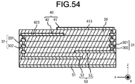
- a resonator 10 illustrated in FIGS. 1 to 62 includes a base 20, pair conductors 30, a third conductor 40, and a fourth conductor 50.
- the base 20 is in contact with the pair conductors 30, the third conductor 40, and the fourth conductor 50.
- the pair conductors 30, the third conductor 40, and the fourth conductor 50 function as a resonator.
- the resonator 10 can be operated in such a manner as to resonate at a plurality of resonant frequencies.
- One of the resonant frequencies of the resonator 10 will be referred to as a first frequency f 1 .
- a wavelength of the first frequency f 1 is ⁇ 1 .
- the resonator 10 can have at least one of the at least one resonant frequency as an operating frequency.
- the resonator 10 uses the first frequency f 1 as the operating frequency.
- the base 20 can include any one of a ceramic material or a resin material as a composition.
- the ceramic material is an aluminum oxide sintered body, an aluminum nitride sintered body, a mullite sintered body, a glass ceramic sintered body, a crystallized glass in which a crystalline component is precipitated in a glass base material, or a microcrystalline sintered body of mica, aluminum titanate, or the like.
- the resin material is an epoxy resin, a polyester resin, a polyimide resin, a polyamideimide resin, a polyetherimide resin, or a material obtained by curing an uncured material such as a liquid crystal polymer.
- the pair conductors 30, the third conductor 40, and the fourth conductor 50 can include, as a composition, any one of a metal material, an alloy of metal materials, a hardened material of a metal paste, or a conductive polymer.
- the pair conductors 30, the third conductor 40, and the fourth conductor 50 may all be formed of the same material.
- the pair conductors 30, the third conductor 40, and the fourth conductor 50 may each be formed of a different material. Any combination of the pair conductors 30, the third conductor 40, and the fourth conductor 50 may be formed of the same material.
- the metal material includes copper, silver, palladium, gold, platinum, aluminum, chromium, nickel, cadmium lead, selenium, manganese, tin, vanadium, lithium, cobalt, titanium, or the like.
- the alloy includes a plurality of metal materials.
- a metal paste is a paste obtained by kneading powder of a metal material with an organic solvent and a binder.
- the binder is an epoxy resin, a polyester resin, a polyimide resin, a polyamideimide resin, or a polyetherimide resin.
- the conductive polymer is a polythiophene-based polymer, a polyacetylene-based polymer, a polyaniline-based polymer, a polypyrrole-based polymer, or the like.
- the resonator 10 includes two pair conductors 30.
- the pair conductors 30 include a plurality of conductors.
- the pair conductors 30 include a first conductor 31 and a second conductor 32.
- the pair conductors 30 can include three or more conductors.
- Each conductor of the pair conductors 30 is separated from another conductor along a first axis.
- Each one of the conductors of the pair conductors 30 can be paired with another conductor.
- Each conductor of the pair conductors 30 can be seen as an electric conductor for the resonator between the paired conductors.
- the first conductor 31 is positioned away from the second conductor 32 along the first axis.
- Each conductor 31 or 32 extends along a second plane that intersects the first axis.
- the first axis is referred to as an x direction.
- a third axis is referred to as a y direction.
- a second axis is referred to as a z direction.
- a first plane is referred to as an xy plane.
- the second plane is referred to as a yz plane.
- a third plane is referred to as a zx plane.
- These planes are planes in a coordinate space, and do not indicate specific plates or specific surfaces.
- a surface integral in the xy plane may be referred to as a first surface integral.
- a surface integral in the yz plane may be referred to as a second surface integral.
- a surface integral in the zx plane may be referred to as a third surface integral.
- the surface integral is expressed in a unit such as a square meter.
- a length in the x direction may be simply referred to as "length”.
- a length in the y direction may be simply referred to as "width”.
- a length in the z direction may be simply referred to as "height".
- the respective conductors 31 and 32 are positioned at opposite end portions of the base 20 in the x direction.
- Each conductor 31 or 32 can partially face the outside of the base 20.
- Each conductor 31 or 32 can be partially positioned inside the base 20, and partially positioned outside the base 20.
- Each conductor 31 or 32 can be positioned inside the base 20.
- the third conductor 40 functions as a resonator.
- the third conductor 40 can include at least one of a line-type resonator, a patch-type resonator, or a slot-type resonator.
- the third conductor 40 is positioned on the base 20.
- the third conductor 40 is positioned at an end of the base 20 in the z direction.
- the third conductor 40 can be positioned inside the base 20.
- the third conductor 40 can be partially positioned inside the base 20, and partially positioned outside the base 20. A partial surface of the third conductor 40 can face the outside of the base 20.
- the third conductor 40 includes at least one conductor.
- the third conductor 40 can include a plurality of conductors. In a case where the third conductor 40 includes a plurality of conductors, the third conductor 40 can be referred to as a third conductor group.
- the third conductor 40 includes at least one conductive layer.
- the third conductor 40 includes at least one conductor in one conductive layer.
- the third conductor 40 can include a plurality of conductive layers.
- the third conductor 40 can include three or more conductive layers.
- the third conductor 40 includes at least one conductor in each of the plurality of conductive layers.
- the third conductor 40 extends in the xy plane.
- the xy plane includes the x direction. Each conductive layer of the third conductor 40 extends along the xy plane.
- the third conductor 40 includes a first conductive layer 41 and a second conductive layer 42.
- the first conductive layer 41 extends along the xy plane.
- the first conductive layer 41 can be positioned on the base 20.
- the second conductive layer 42 extends along the xy plane.
- the second conductive layer 42 can be capacitively coupled to the first conductive layer 41.
- the second conductive layer 42 can be electrically connected to the first conductive layer 41.
- Two conductive layers capacitively coupled to each other may face each other in the y direction.
- Two conductive layers capacitively coupled to each other may face each other in the x direction.
- Two conductive layers capacitively coupled to each other may face each other in the first plane.
- Two conductive layers facing each other in the first plane can be paraphrased as two conductors in one conductive layer.
- the second conductive layer 42 can be positioned such that at least a portion thereof overlaps the first conductive layer 41 in the z direction.
- the second conductive layer 42 can be positioned inside the base 20.
- the fourth conductor 50 is positioned away from the third conductor 40.
- the fourth conductor 50 is electrically connected to each conductor 31 or 32 of the pair conductors 30.
- the fourth conductor 50 is electrically connected to the first conductor 31 and the second conductor 32.
- the fourth conductor 50 extends along the third conductor 40.
- the fourth conductor 50 extends along the first plane.
- the fourth conductor 50 extends from the first conductor 31 to the second conductor 32.
- the fourth conductor 50 is positioned on the base 20.
- the fourth conductor 50 may be positioned inside the base 20.
- the fourth conductor 50 can be partially positioned inside the base 20, and partially positioned outside the base 20. A partial surface of the fourth conductor 50 can face the outside of the base 20.
- the fourth conductor 50 can function as a ground conductor in the resonator 10.
- the fourth conductor 50 can serve as an electric potential reference point for the resonator 10.
- the fourth conductor 50 may be connected to a ground of a device including the resonator 10.
- the resonator 10 can include the fourth conductor 50 and a reference potential layer 51.
- the reference potential layer 51 is positioned away from the fourth conductor 50 in the z direction.
- the reference potential layer 51 is electrically insulated from the fourth conductor 50.
- the reference potential layer 51 can serve as an electric potential reference point for the resonator 10.
- the reference potential layer 51 can be electrically connected to the ground of the device including the resonator 10.
- the fourth conductor 50 can be electrically separated from the ground of the device including the resonator 10.
- the reference potential layer 51 faces any one of the third conductor 40 or the fourth conductor 50 in the z direction.
- the reference potential layer 51 faces the third conductor 40 while having the fourth conductor 50 interposed therebetween.
- the fourth conductor 50 is positioned between the third conductor 40 and the reference potential layer 51.
- An interval between the reference potential layer 51 and the fourth conductor 50 is smaller than an interval between the third conductor 40 and the fourth conductor 50.
- the fourth conductor 50 can include one or more conductors.
- the fourth conductor 50 can include one or more conductors, and the third conductor 40 can be one conductor connected to the pair conductors 30.
- each of the third conductor 40 and the fourth conductor 50 can include at least one resonator.
- the fourth conductor 50 can include a plurality of conductive layers.
- the fourth conductor 50 can include a third conductive layer 52 and a fourth conductive layer 53.
- the third conductive layer 52 can be capacitively coupled to the fourth conductive layer 53.
- the third conductive layer 52 can be electrically connected to the first conductive layer 41.
- Two conductive layers capacitively coupled to each other may face each other in the y direction.
- Two conductive layers capacitively coupled to each other may face each other in the x direction.
- Two conductive layers capacitively coupled to each other may face each other in the xy plane.
- a distance between two conductive layers facing each other in the z direction and capacitively coupled to each other is smaller than a distance between a corresponding conductor group and the reference potential layer 51.
- a distance between the first conductive layer 41 and the second conductive layer 42 is smaller than a distance between the third conductor 40 and the reference potential layer 51.
- a distance between the third conductive layer 52 and the fourth conductive layer 53 is smaller than a distance between the fourth conductor 50 and the reference potential layer 51.
- Each of the first conductor 31 and the second conductor 32 can include one or more conductors.
- Each of the first conductor 31 and the second conductor 32 can be one conductor.
- Each of the first conductor 31 and the second conductor 32 can include a plurality of conductors.
- Each of the first conductor 31 and the second conductor 32 can include at least one fifth conductive layer 301 and a plurality of fifth conductors 302.
- the pair conductors 30 include at least one fifth conductive layer 301 and a plurality of fifth conductors 302.
- the fifth conductive layer 301 extends in the y direction.
- the fifth conductive layer 301 extends along the xy plane.
- the fifth conductive layer 301 is a conductor having a layer form.
- the fifth conductive layer 301 can be positioned on the base 20.
- the fifth conductive layer 301 can be positioned inside the base 20.
- the plurality of fifth conductive layers 301 are separated from each other in the z direction.
- the plurality of fifth conductive layers 301 are arranged in the z direction.
- the plurality of fifth conductive layers 301 partially overlap each other in the z direction.
- the fifth conductive layer 301 electrically connects the plurality of fifth conductors 302.
- the fifth conductive layer 301 is a connecting conductor that connects the plurality of fifth conductors 302.
- the fifth conductive layer 301 can be electrically connected to any conductive layer of the third conductor 40. In embodiments, the fifth conductive layer 301 is electrically connected to the second conductive layer 42. The fifth conductive layer 301 can be integrated with the second conductive layer 42. In embodiments, the fifth conductive layer 301 can be electrically connected to the fourth conductor 50. The fifth conductive layer 301 can be integrated with the fourth conductor 50.
- Each fifth conductor 302 extends in the z direction.
- the plurality of fifth conductors 302 are separated from each other in the y direction.
- a distance between the fifth conductors 302 is equal to or smaller than 1/2 of the wavelength ⁇ 1 .
- each of the first conductor 31 and the second conductor 32 can reduce the leakage of electromagnetic waves in a resonant frequency band from between the fifth conductors 302. Since the leakage of electromagnetic waves in the resonant frequency band is reduced, the pair conductors 30 are seen as electric conductors for a unit structure. At least some of the plurality of fifth conductors 302 are electrically connected to the fourth conductor 50.
- some of the plurality of fifth conductors 302 can electrically connect the fourth conductor 50 and the fifth conductive layer 301 to each other. In embodiments, the plurality of fifth conductors 302 can be electrically connected to the fourth conductor 50 via the fifth conductive layer 301. Some of the plurality of fifth conductors 302 can electrically connect one fifth conductive layer 301 and another fifth conductive layer 301 to each other. The fifth conductor 302 can use a via conductor and a through-hole conductor.
- the resonator 10 includes the third conductor 40 that functions as a resonator.
- the third conductor 40 can function as an artificial magnetic conductor (AMC).
- the artificial magnetic conductor can also be referred to as a reactive impedance surface (RIS).
- the resonator 10 includes the third conductor 40 that functions as a resonator and is provided between two pair conductors 30 facing each other in the x direction.
- the two pair conductors 30 can be seen as electric conductors extending in the yz plane for the third conductor 40. Ends of the resonator 10 in the y direction are electrically opened.
- zx planes at the opposite ends in the y direction are in a high impedance state.
- the zx planes at the opposite ends of the resonator 10 in the y direction are seen as magnetic conductors for the third conductor 40.
- the resonator 10 is surrounded by two electric conductors and two high impedance surfaces (magnetic conductors), so that the resonator of the third conductor 40 has an artificial magnetic conductor character in the z direction. Since the resonator 10 is surrounded by two electric conductors and two high impedance surfaces, the resonator of the third conductor 40 has the artificial magnetic conductor character with a finite value.
- a phase difference between an incident wave and a reflected wave at the operating frequency is 0 degrees.
- a phase difference between the incident wave and the reflected wave at the first frequency f 1 is 0 degrees.
- a phase difference between the incident wave and the reflected wave in an operating frequency band is - 90 degrees to +90 degrees.
- the operating frequency band is a frequency band between a second frequency f 2 and a third frequency f 3 .
- the second frequency f 2 is a frequency at which the phase difference between the incident wave and the reflected wave is +90 degrees.
- the third frequency f 3 is a frequency at which the phase difference between the incident wave and the reflected wave is -90 degrees.
- the width of the operating frequency band determined based on the second and third frequencies may be, for example, 100 MHz or more when the operating frequency is about 2.5 GHz.
- the width of the operating frequency band may be, for example, 5 MHz or more when the operating frequency is about 400 MHz.
- the operating frequency of the resonator 10 can be different from the resonant frequency of each resonator of the third conductor 40.
- the operating frequency of the resonator 10 can vary depending on the length, size, shape, material, and the like of each of the base 20, the pair conductors 30, the third conductor 40, and the fourth conductor 50.
- the third conductor 40 can include at least one unit resonator 40X.
- the third conductor 40 can include one unit resonator 40X.
- the third conductor 40 can include a plurality of unit resonators 40X.
- the unit resonator 40X is positioned in such a manner as to overlap the fourth conductor 50 in the z direction.
- the unit resonator 40X faces the fourth conductor 50.
- the unit resonator 40X can function as a frequency selective surface (FSS).
- the plurality of unit resonators 40X are arranged along the xy plane.
- the plurality of unit resonators 40X can be regularly arranged in the xy plane.
- the unit resonators 40X can be arranged in a square grid, an oblique grid, a rectangular grid, or a hexagonal grid.
- the third conductor 40 can include a plurality of conductive layers arranged in the z direction. Each of the plurality of conductive layers of the third conductor 40 includes parts equivalent to at least one unit resonator.
- the third conductor 40 includes a first conductive layer 41 and a second conductive layer 42.
- the first conductive layer 41 includes parts equivalent to at least one first unit resonator 41X.
- the first conductive layer 41 can include one first unit resonator 41X.
- the first conductive layer 41 can include a plurality of first divisional resonators 41Y subdivided from one first unit resonator 41X.
- the plurality of first divisional resonators 41Y can form at least one first unit resonator 41X by an adjacent unit structure 10X.
- the plurality of first divisional resonators 41Y are positioned at end portions of the first conductive layer 41.
- the first unit resonator 41X and the first divisional resonator 41Y can be referred to as the third conductor.
- the second conductive layer 42 includes parts equivalent to at least one second unit resonator 42X.
- the second conductive layer 42 can include one second unit resonator 42X.
- the second conductive layer 42 can include a plurality of second divisional resonators 42Y subdivided from one second unit resonator 42X.
- the plurality of second divisional resonators 42Y can form at least one second unit resonator 42X by an adjacent unit structure 10X.
- the plurality of second divisional resonators 42Y are positioned at end portions of the second conductive layer 42.
- the second unit resonator 42X and the second divisional resonator 42Y can be referred to as the third conductor.
- At least portions of the second unit resonator 42X and the second divisional resonator 42Y are positioned in such a manner as to overlap the first unit resonator 41X and the first divisional resonator 41Y in the Z direction.
- the third conductor 40 at least portions of the unit resonator and the divisional resonator of each layer overlap with each other in the Z direction and form one unit resonator 40X.
- the unit resonator 40X includes parts equivalent to at least one unit resonator in each layer.
- the first conductive layer 41 includes at least one first unit conductor 411.
- the first unit conductor 411 can function as the first unit resonator 41X or the first divisional resonator 41Y.
- the first conductive layer 41 includes a plurality of first unit conductors 411 arranged in n rows and m columns in the x direction and the y direction. n and m are natural numbers of 1 or more, which are independent of each other. In the example illustrated in FIGS. 1 to 9 and the like, the first conductive layer 41 includes six first unit conductors 411 arranged in a grid pattern of two rows and three columns.
- the first unit conductors 411 can be arranged in a square grid, an oblique grid, a rectangular grid, or a hexagonal grid.
- the first unit conductor 411 corresponding to the first divisional resonator 41Y is positioned at an end portion of the first conductive layer 41 in the xy plane.
- the first unit resonator 41X is a slot-type resonator
- the first conductive layer 41 at least one conductive layer extends in the x direction and the y direction.
- the first conductive layer 41 includes at least one first unit slot 412.
- the first unit slot 412 can function as the first unit resonator 41X or the first divisional resonator 41Y.
- the first conductive layer 41 can include a plurality of first unit slots 412 arranged in n rows and m columns in the x direction and the y direction. n and m are natural numbers of 1 or more, which are independent of each other. In the example illustrated in FIGS.
- the first conductive layer 41 includes six first unit slots 412 arranged in a grid pattern of two rows and three columns.
- the first unit slots 412 can be arranged in a square grid, an oblique grid, a rectangular grid, or a hexagonal grid.
- the first unit slot 412 corresponding to the first divisional resonator 41Y is positioned at an end portion of the first conductive layer 41 in the xy plane.
- the second conductive layer 42 includes at least one second unit conductor 421.
- the second conductive layer 42 can include a plurality of second unit conductors 421 arranged in the x direction and the y direction.
- the second unit conductors 421 can be arranged in a square grid, an oblique grid, a rectangular grid, or a hexagonal grid.
- the second unit conductor 421 can function as the second unit resonator 42X or the second divisional resonator 42Y.
- the second unit conductor 421 corresponding to the second divisional resonator 42Y is positioned at an end portion of the second conductive layer 42 in the xy plane.
- At least a portion of the second unit conductor 421 overlaps at least one of the first unit resonator 41X or the first divisional resonator 41Y in the z direction.
- the second unit conductor 421 can overlap the plurality of first unit resonators 41X.
- the second unit conductor 421 can overlap the plurality of first divisional resonators 41Y.
- the second unit conductor 421 can overlap one first unit resonator 41X and four first divisional resonators 41Y.
- the second unit conductor 421 can overlap only one first unit resonator 41X.
- the center of gravity of the second unit conductor 421 can overlap one first unit resonator 41X.
- the center of gravity of the second unit conductor 421 can be positioned between the plurality of first unit resonators 41X and the first divisional resonator 41Y.
- the center of gravity of the second unit conductor 421 can be positioned between two first unit resonators 41X arranged in the x direction or the y direction.
- At least a portion of the second unit conductor 421 can overlap two first unit conductors 411.
- the second unit conductor 421 can overlap only one first unit conductor 411.
- the center of gravity of the second unit conductor 421 can be positioned between two first unit conductors 411.
- the center of gravity of the second unit conductor 421 can overlap one first unit conductor 411.
- At least a portion of the second unit conductor 421 can overlap the first unit slot 412.
- the second unit conductor 421 can overlap only one first unit slot 412.
- the center of gravity of the second unit conductor 421 can be positioned between two first unit slots 412 arranged in the x direction or the y direction.
- the center of gravity of the second unit conductor 421 can overlap one first unit slot 412.
- the second unit resonator 42X is a slot-type resonator
- the second conductive layer 42 includes at least one second unit slot 422.
- the second unit slot 422 can function as the second unit resonator 42X or the second divisional resonator 42Y.
- the second conductive layer 42 can include a plurality of second unit slots 422 arranged in the xy plane.
- the second unit slots 422 can be arranged in a square grid, an oblique grid, a rectangular grid, or a hexagonal grid.
- the second unit slot 422 corresponding to the second divisional resonator 42Y is positioned at an end portion of the second conductive layer 42 in the xy plane.
- At least a portion of the second unit slot 422 overlaps at least one of the first unit resonator 41X or the first divisional resonator 41Y in the y direction.
- the second unit slot 422 can overlap the plurality of first unit resonators 41X.
- the second unit slot 422 can overlap the plurality of first divisional resonators 41Y.
- the second unit slot 422 can overlap one first unit resonator 41X and four first divisional resonators 41Y.
- the second unit slot 422 can overlap only one first unit resonator 41X.
- the center of gravity of the second unit slot 422 can overlap one first unit resonator 41X.
- the center of gravity of the second unit slot 422 can be positioned between the plurality of first unit resonators 41X.
- the center of gravity of the second unit slot 422 can be positioned between one first unit resonator 41X and one first divisional resonator 41Y arranged in the x direction or the y direction.
- At least a portion of the second unit slot 422 can overlap two first unit conductors 411.
- the second unit slot 422 can overlap only one first unit conductor 411.
- the center of gravity of the second unit slot 422 can be positioned between two first unit conductors 411.
- the center of gravity of the second unit slot 422 may overlap one first unit conductor 411.
- At least a portion of the second unit slot 422 can overlap the first unit slot 412.
- the second unit slot 422 can overlap only one first unit slot 412.
- the center of gravity of the second unit slot 422 can be positioned between two first unit slots 412 arranged in the x direction or the y direction.
- the center of the second unit slot 422 can overlap one first unit slot 412.
- the unit resonator 40X includes parts equivalent to at least one first unit resonator 41X and parts equivalent to at least one second unit resonator 42X.
- the unit resonator 40X can include one first unit resonator 41X.
- the unit resonator 40X can include a plurality of first unit resonators 41X.
- the unit resonator 40X can include one first divisional resonator 41Y.
- the unit resonator 40X can include a plurality of first divisional resonators 41Y.
- the unit resonator 40X can include a portion of the first unit resonator 41X.
- the unit resonator 40X can include one or more partial first unit resonators 41X.
- the unit resonator 40X includes a plurality of partial resonators of one or more partial first unit resonators 41X and one or more first divisional resonators 41Y.
- the plurality of partial resonators included in the unit resonator 40X are combined into at least one first unit resonator 41X.
- the unit resonator 40X can include a plurality of first divisional resonators 41Y without including the first unit resonator 41X.
- the unit resonator 40X can include, for example, four first divisional resonators 41Y.
- the unit resonator 40X can include only a plurality of partial first unit resonators 41X.
- the unit resonator 40X can include one or more partial first unit resonators 41X and one or more first divisional resonators 41Y.
- the unit resonator 40X can include, for example, two partial first unit resonators 41X and two first divisional resonators 41Y.
- the unit resonator 40X can have substantially the same mirror image of the included first conductive layer 41 at opposite ends of the unit resonator 40X in the x direction.
- the included first conductive layer 41 can be substantially symmetrical with respect to the center line extending in the z direction.
- the unit resonator 40X can include one second unit resonator 42X.
- the unit resonator 40X can include a plurality of second unit resonators 42X.
- the unit resonator 40X can include one second divisional resonator 42Y.
- the unit resonator 40X can include a plurality of second divisional resonators 42Y.
- the unit resonator 40X can include a portion of the second unit resonator 42X.
- the unit resonator 40X can include one or more partial second unit resonators 42X.
- the unit resonator 40X includes a plurality of partial resonators of one or more partial second unit resonators 42X and one or more second divisional resonators 42Y.
- the plurality of partial resonators included in the unit resonator 40X are combined into at least one second unit resonator 42X.
- the unit resonator 40X can include a plurality of second divisional resonators 42Y without including the second unit resonator 42X.
- the unit resonator 40X can include, for example, four second divisional resonators 42Y.
- the unit resonator 40X can include only a plurality of partial second unit resonators 42X.
- the unit resonator 40X can include one or more partial second unit resonators 42X and one or more second divisional resonators 42Y.
- the unit resonator 40X can include, for example, two partial second unit resonators 42X and two second divisional resonators 42Y.
- the unit resonator 40X can have substantially the same mirror image of the included second conductive layer 42 at opposite ends of the unit resonator 40X in the x direction.
- the included second conductive layer 42 can be substantially symmetrical with respect to the center line extending in the y direction.
- the unit resonator 40X includes one first unit resonator 41X and a plurality of partial second unit resonators 42X.
- the unit resonator 40X includes one first unit resonator 41X and half of four second unit resonators 42X.
- the unit resonator 40X includes parts equivalent to one first unit resonator 41X and parts equivalent to two second unit resonators 42X. Components included in the unit resonator 40X are not limited to this example.
- the resonator 10 can include at least one unit structure 10X.
- the resonator 10 can include a plurality of unit structures 10X.
- the plurality of unit structures 10X can be arranged in the xy plane.
- the plurality of unit structures 10X can be arranged in a square grid, an oblique grid, a rectangular grid, or a hexagonal grid.
- the unit structure 10X includes a repeating unit of any one of a square grid, an oblique grid, a rectangular grid, or a hexagonal grid.
- the unit structures 10X can function as artificial magnetic conductors (AMC) when arranged infinitely in the xy plane.
- AMC artificial magnetic conductors
- the unit structure 10X can include at least a portion of the base 20, at least a portion of the third conductor 40, and at least a portion of the fourth conductor 50. Portions of the base 20, the third conductor 40, and the fourth conductor 50 included in the unit structure 10X overlap in the z direction.
- the unit structure 10X includes the unit resonator 40X, a portion of the base 20 that overlaps the unit resonator 40X in the z direction, and the fourth conductor 50 that overlaps the unit resonator 40X in the z direction.
- the resonator 10 can include, for example, six unit structures 10X arranged in two rows and three columns.
- the resonator 10 can include at least one unit structure 10X between two pair conductors 30 facing each other in the x direction.
- the two pair conductors 30 can be seen as electric conductors extending in the yz plane for the unit structure 10X. Ends of the unit structure 10X in the y direction are opened.
- zx planes at the opposite ends in the y direction are in a high impedance state.
- the zx planes at the opposite ends in the y direction can be seen as magnetic conductors.
- the unit structures 10X may have a line symmetry with respect to the z direction when repeatedly arranged.
- the unit structure 10X Since the unit structure 10X is surrounded by two electric conductors and two high impedance surfaces (magnetic conductors), the unit structure 10X has an artificial magnetic conductor character in the z direction. Since the unit structure 10X is surrounded by two electric conductors and two high impedance surfaces (magnetic conductors), the unit structure 10X has the artificial magnetic conductor character with a finite value.
- the operating frequency of the resonator 10 can be different from the operating frequency of the first unit resonator 41X.
- the operating frequency of the resonator 10 can be different from the operating frequency of the second unit resonator 42X.
- the operating frequency of the resonator 10 can be changed by the coupling of the first unit resonator 41X and the second unit resonator 42X that form the unit resonator 40X, or the like.
- the third conductor 40 can include the first conductive layer 41 and the second conductive layer 42.
- the first conductive layer 41 includes at least one first unit conductor 411.
- the first unit conductor 411 includes a first connecting conductor 413 and a first floating conductor 414.
- the first connecting conductor 413 is connected to any one of the pair conductors 30.
- the first floating conductor 414 is not connected to the pair conductors 30.
- the second conductive layer 42 includes at least one second unit conductor 421.
- the second unit conductor 421 includes a second connecting conductor 423 and a second floating conductor 424.
- the second connecting conductor 423 is connected to any one of the pair conductors 30.
- the second floating conductor 424 is not connected to the pair conductors 30.
- the third conductor 40 can include the first unit conductor 411 and the second unit conductor 421.
- the first connecting conductor 413 can have a length larger than that of the first floating conductor 414 in the x direction.
- the first connecting conductor 413 can have a length smaller than that of the first floating conductor 414 in the x direction.
- the first connecting conductor 413 can have a length that is half that of the first floating conductor 414 in the x direction.
- the second connecting conductor 423 can have a length larger than that of the second floating conductor 424 in the x direction.
- the second connecting conductor 423 can have a length smaller than that of the second floating conductor 424 in the x direction.
- the second connecting conductor 423 can have a length that is half that of the second floating conductor 424 in the x direction.
- the third conductor 40 can include a current path 401 that serves as a current path between the first conductor 31 and the second conductor 32 when the resonator 10 resonates.
- the current path 401 can be connected to the first conductor 31 and the second conductor 32.
- the current path 401 has a capacitance between the first conductor 31 and the second conductor 32.
- the capacitance of the current path 401 is electrically connected in series between the first conductor 31 and the second conductor 32.
- a conductor is positioned between the first conductor 31 and the second conductor 32 while being in a separated state.
- the current path 401 can include a conductor connected to the first conductor 31 and a conductor connected to the second conductor 32.
- the first unit conductor 411 and the second unit conductor 421 partially face each other in the z direction.
- the first unit conductor 411 and the second unit conductor 421 are capacitively coupled to each other.
- the first unit conductor 411 includes a capacitive component at an end portion in the x direction.
- the first unit conductor 411 can include a capacitive component at an end portion in the y direction that faces the second unit conductor 421 in the z direction.
- the first unit conductor 411 can include capacitive components at an end portion in the x direction that faces the second unit conductor 421 in the z direction and at an end portion in the y direction.
- the second unit conductor 421 includes a capacitive component at an end portion in the x direction.
- the second unit conductor 421 can include a capacitive component at an end portion in the y direction that faces the first unit conductor 411 in the z direction.
- the second unit conductor 421 can include capacitive components at an end portion in the x direction that faces the first unit conductor 411 in the z direction and at an end portion in the y direction.
- the resonator 10 can reduce the resonant frequency by increasing the capacitive coupling in the current path 401.
- the resonator 10 can reduce the length in the x direction by increasing the capacitive coupling in the current path 401.
- the first unit conductor 411 and the second unit conductor 421 face each other in a stacking direction of the base 20 and are capacitively coupled to each other.
- the capacitance between the first unit conductor 411 and the second unit conductor 421 can be adjusted by a surface integral of an area by which the first unit conductor 411 and the second unit conductor 421 face each other.
- the length of the first unit conductor 411 in the y direction is different from the length of the second unit conductor 421 in the y direction.
- a change in magnitude of the capacitance can be reduced due to a difference in length along the third axis between the first unit conductor 411 and the second unit conductor 421.
- the current path 401 includes one conductor that is spatially separated from the first conductor 31 and the second conductor 32 and is capacitively coupled to the first conductor 31 and the second conductor 32.
- the current path 401 includes the first conductive layer 41 and the second conductive layer 42.
- the current path 401 includes at least one first unit conductor 411 and at least one second unit conductor 421.
- the current path 401 includes two first connecting conductors 413, two second connecting conductors 423, and one first connecting conductor 413 or one second connecting conductor 423.
- the first unit conductor 411 and the second unit conductor 421 can be arranged alternately along the first axis.
- the current path 401 includes the first connecting conductor 413 and the second connecting conductor 423.
- the current path 401 includes at least one first connecting conductor 413 and at least one second connecting conductor 423.
- the third conductor 40 has a capacitance between the first connecting conductor 413 and the second connecting conductor 423.
- the first connecting conductor 413 can face the second connecting conductor 423 and have a capacitance.
- the first connecting conductor 413 can be capacitively connected to the second connecting conductor 423 via another conductor.
- the current path 401 includes the first connecting conductor 413 and the second floating conductor 424.
- the current path 401 includes two first connecting conductors 413.
- the third conductor 40 has a capacitance between two first connecting conductors 413.
- two first connecting conductors 413 can be capacitively connected to each other via at least one second floating conductor 424.
- two first connecting conductors 413 can be capacitively connected to each other via at least one first floating conductor 414 and a plurality of second floating conductors 424.
- the current path 401 includes the first floating conductor 414 and the second connecting conductor 423.
- the current path 401 includes two second connecting conductors 423.
- the third conductor 40 has a capacitance between two second connecting conductors 423.
- two second connecting conductors 423 can be capacitively connected to each other via at least one first floating conductor 414.
- two second connecting conductors 423 can be capacitively connected to each other via a plurality of first floating conductors 414 and at least one second floating conductor 424.
- the first connecting conductor 413 and the second connecting conductor 423 can each have a length corresponding to 1/4 of the wavelength ⁇ at the resonant frequency.
- the first connecting conductor 413 and the second connecting conductor 423 can each function as a resonator having a length corresponding to a half of the wavelength ⁇ .
- the first connecting conductor 413 and the second connecting conductor 423 can each be operated in such a manner as to oscillate in an odd mode and an even mode due to capacitive coupling of the respective resonators.
- the resonator 10 can use, as the operating frequency, a resonant frequency in the even mode after the capacitive coupling.
- the current path 401 can be connected to the first conductor 31 at a plurality of points.
- the current path 401 can be connected to the second conductor 32 at a plurality of points.
- the current path 401 can include a plurality of conductive paths that independently conduct electricity from the first conductor 31 to the second conductor 32.
- a distance between an end of the second floating conductor 424 on the side where the capacitive coupling is made and the first connecting conductor 413 is smaller than a distance between the end of the second floating conductor 424 and the pair conductors 30.
- a distance between an end of the first floating conductor 414 on the side where the capacitive coupling is made and the second connecting conductor 423 is smaller than a distance between the end of the first floating conductor 414 and the pair conductors 30.
- each conductive layer of the third conductor 40 can have a different length in the y direction.
- the conductive layer of the third conductor 40 is capacitively coupled to another conductive layer in the z direction.
- a change in capacitance is reduced even in a case where the conductive layer is displaced in the y direction. Since each conductive layer of the resonator 10 has a different length in the y direction, it is possible to widen an allowable range of the displacement of the conductive layer in the y direction.
- the third conductor 40 has a capacitance due to capacitive coupling between the conductive layers.
- a plurality of capacitive portions having the capacitance can be arranged in the y direction.
- the plurality of capacitive portions arranged in the y direction can have an electromagnetically parallel relationship.
- the resonator 10 has a plurality of capacitive portions that are arranged in electrically parallel with each other, individual capacitive errors can be mutually complemented.
- the resonator 10 When the resonator 10 is in a resonance state, a current flowing through the pair conductors 30, the third conductor 40, and the fourth conductor 50 loops. When the resonator 10 is in a resonance state, an alternating current flows through the resonator 10. In the resonator 10, the current flowing through the third conductor 40 is a first current, and the current flowing through the fourth conductor 50 is a second current. When the resonator 10 is in a resonance state, the first current flows toward a direction different from that of the second current in the x direction. For example, when the first current flows in the +x direction, the second current flows in the -x direction. For example, when the first current flows in the -x direction, the second current flows in the +x direction.
- a loop current alternately flows in the +x direction and the -x direction.
- the resonator 10 radiates electromagnetic waves by repeating reversal of a loop current that forms a magnetic field.
- the third conductor 40 includes the first conductive layer 41 and the second conductive layer 42. Since the first conductive layer 41 and the second conductive layer 42 are capacitively coupled to each other in the third conductor 40, it seems that a current flows over a large area in one direction in a resonance state. In embodiments, a current flowing through each conductor has a high density at an end portion in the y direction.
- the first conductor 31, the second conductor 32, the third conductor 40, and the fourth conductor 50 form a resonant circuit.
- the resonant frequency of the resonator 10 is the resonant frequency of the unit resonator.
- the resonant frequency of the resonator 10 is changed by electromagnetic coupling with the base 20, the pair conductors 30, the third conductor 40, the fourth conductor 50, and the periphery of the resonator 10.
- the entire resonator 10 forms one unit resonator or a portion of one unit resonator.
- the resonant frequency of the resonator 10 is changed depending on the lengths of the first conductor 31 and the second conductor 32 in the z direction, the lengths of the third conductor 40 and the fourth conductor 50 in the x direction, the capacitances of the third conductor 40 and the fourth conductor 50.
- the lengths of the first conductor 31 and the second conductor 32 in the z direction, and the lengths of the third conductor 40 and the fourth conductor 50 in the x direction can be reduced while reducing the resonant frequency.
- the first conductive layer 41 serves as an effective radiation surface for electromagnetic waves in the z direction.
- the first surface integral of the first conductive layer 41 is larger than the first surface integral of another conductive layer. The resonator 10 can increase the radiation of electromagnetic waves by increasing the first surface integral of the first conductive layer 41.
- the resonator 10 can include one or more impedance elements 45.
- the impedance element 45 has an impedance value between a plurality of terminals.
- the impedance element 45 changes the resonant frequency of the resonator 10.
- the impedance element 45 can include a register, a capacitor, and an inductor.
- the impedance element 45 can include a variable element whose impedance value can be changed.
- the variable element can change the impedance value according to an electric signal.
- the variable element can change the impedance value by a physical mechanism.
- the impedance element 45 can be connected to two unit conductors of the third conductor 40 that are arranged in the x direction.
- the impedance element 45 can be connected to two first unit conductors 411 arranged in the x direction.
- the impedance element 45 can be connected to the first connecting conductor 413 and the first floating conductor 414 arranged in the x direction.
- the impedance element 45 can be connected to the first conductor 31 and the first floating conductor 414.
- the impedance element 45 is connected to the unit conductor of the third conductor 40 at a central portion in the y direction.
- the impedance element 45 is connected to a central portion of each of two first unit conductors 411 in the y direction.
- the impedance element 45 is electrically connected in series between two conductors arranged in the x direction in the xy plane.
- the impedance element 45 can be electrically connected in series between two first unit conductors 411 arranged in the x direction.
- the impedance element 45 can be electrically connected in series between the first connecting conductor 413 and the first floating conductor 414 arranged in the x direction.
- the impedance element 45 can be electrically connected in series between the first conductor 31 and the first floating conductor 414.
- the impedance element 45 can be electrically connected in parallel with the first unit conductors 411 and the second unit conductor 421 that overlap each other in the z direction and have a capacitance.
- the impedance element 45 can be electrically connected in parallel with the second connecting conductor 423 and the first floating conductor 414 that overlap each other in the z direction and have a capacitance.
- the resonator 10 can reduce the resonant frequency by adding a capacitor as the impedance element 45.
- the resonator 10 can increase the resonant frequency by adding an inductor as the impedance element 45.
- the resonator 10 can include impedance elements 45 with different impedance values.
- the resonator 10 can include capacitors with different electric capacities as the impedance elements 45.
- the resonator 10 can include inductors with different inductances as the impedance elements 45. In the resonator 10, an adjustment range of the resonant frequency is increased by adding impedance elements 45 with different impedance values.
- the resonator 10 can include both a capacitor and an inductor as the impedance elements 45.
- the adjustment range of the resonant frequency is increased by adding both a capacitor and an inductor as the impedance elements 45.
- the resonator 10 includes the impedance element 45, the entire resonator 10 can form one unit resonator, or a portion of one unit resonator.
- FIGS. 1 to 5 are views each illustrating the resonator 10 as an example of embodiments.
- FIG. 1 is a schematic view of the resonator 10.
- FIG. 2 is a plan view illustrating the xy plane viewed from the z direction.
- FIG. 3A is a cross-sectional view taken along line IIIa-IIIa illustrated in FIG. 2 .
- FIG. 3B is a cross-sectional view taken along line IIIb-IIIb illustrated in FIG. 2 .
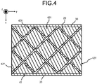
- FIG. 4 is a cross-sectional view taken along line IV-IV illustrated in FIGS. 3A and 3B .
- FIG. 5 is a conceptual view illustrating the unit structure 10X as an example of embodiments.
- the first conductive layer 41 includes a patch-type resonator as the first unit resonator 41X.
- the second conductive layer 42 includes a patch-type resonator as the second unit resonator 42X.
- the unit resonator 40X includes one first unit resonator 41X and four second divisional resonators 42Y.
- the unit structure 10X includes the unit resonator 40X, and a portion of the base 20 and a portion of the fourth conductor 50 that overlap the unit resonator 40X in the z direction.
- FIGS. 6 to 9 are views each illustrating the resonator 10 as an example of embodiments.
- FIG. 6 is a schematic view of the resonator 10.
- FIG. 7 is a plan view illustrating the xy plane viewed from the z direction.
- FIG. 8A is a cross-sectional view taken along line VIIIa-VIIIa illustrated in FIG. 7 .
- FIG. 8B is a cross-sectional view taken along line VIIIb-VIIIb illustrated in FIG. 7 .
- FIG. 9 is a cross-sectional view taken along line IX-IX illustrated in FIGS. 8A and 8B .
- the first conductive layer 41 includes a slot-type resonator as the first unit resonator 41X.
- the second conductive layer 42 includes a slot-type resonator as the second unit resonator 42X.
- the unit resonator 40X includes one first unit resonator 41X and four second divisional resonators 42Y.
- the unit structure 10X includes the unit resonator 40X, and a portion of the base 20 and a portion of the fourth conductor 50 that overlap the unit resonator 40X in the z direction.
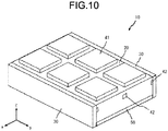
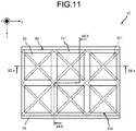
- FIGS. 10 to 13 are views each illustrating the resonator 10 as an example of embodiments.
- FIG. 10 is a schematic view of the resonator 10.
- FIG. 11 is a plan view illustrating the xy plane viewed from the z direction.
- FIG. 12A is a cross-sectional view taken along line XIIa-XIIa illustrated in FIG. 11 .
- FIG. 12B is a cross-sectional view taken along line XIIb-XIIb illustrated in FIG. 11 .
- FIG. 13 is a cross-sectional view taken along line XIII-XIII illustrated in FIGS. 12A and 12B .
- the first conductive layer 41 includes a patch-type resonator as the first unit resonator 41X.
- the second conductive layer 42 includes a slot-type resonator as the second unit resonator 42X.
- the unit resonator 40X includes one first unit resonator 41X and four second divisional resonators 42Y.
- the unit structure 10X includes the unit resonator 40X, and a portion of the base 20 and a portion of the fourth conductor 50 that overlap the unit resonator 40X in the z direction.
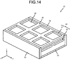
- FIGS. 14 to 17 are views each illustrating the resonator 10 as an example of embodiments.
- FIG. 14 is a schematic view of the resonator 10.
- FIG. 15 is a plan view illustrating the xy plane viewed from the z direction.
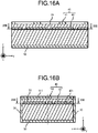
- FIG. 16A is a cross-sectional view taken along line XVIa-XVIa illustrated in FIG. 15 .
- FIG. 16B is a cross-sectional view taken along line XVIb-XVIb illustrated in FIG. 15 .
- FIG. 17 is a cross-sectional view taken along line XVII-XVII illustrated in FIGS. 16A and 16B .
- the first conductive layer 41 includes a slot-type resonator as the first unit resonator 41X.
- the second conductive layer 42 includes a patch-type resonator as the second unit resonator 42X.
- the unit resonator 40X includes one first unit resonator 41X and four second divisional resonators 42Y.
- the unit structure 10X includes the unit resonator 40X, and a portion of the base 20 and a portion of the fourth conductor 50 that overlap the unit resonator 40X in the z direction.
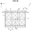
- FIG. 18 is a view illustrating the resonator 10 including pair conductors 30 having another configuration.
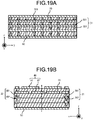
- FIG. 19A is a cross-sectional view taken along line XIXa-XIXa illustrated in FIG. 18 .
- FIG. 19B is a cross-sectional view taken along line XIXb-XIXb illustrated in FIG. 18 .
- the base 20 illustrated in each of FIGS. 1 to 19 is an example.
- the configuration of the base 20 is not limited to the configurations illustrated in FIGS. 1 to 19 .
- the base 20 can have a cavity 20a therein, as illustrated in FIG. 20 .
- the cavity 20a is positioned between the third conductor 40 and the fourth conductor 50 in the z direction.
- the dielectric constant in the cavity 20a is lower than that of the base 20. Since the base 20 has the cavity 20a, an electromagnetic distance between the third conductor 40 and the fourth conductor 50 can be shortened.
- the base 20 can include a plurality of members, as illustrated in FIG. 21 .
- the base 20 can include a first base 21, a second base 22, and a connector 23.
- the first base 21 and the second base 22 can be mechanically connected via the connector 23.
- the connector 23 can include a sixth conductor 303 therein.
- the sixth conductor 303 is electrically connected to the fourth conductor 301 or the fifth conductor 302.
- the sixth conductor 303 forms the first conductor 31 or the second conductor 32, in combination with the fourth conductor 301 and the fifth conductor 302.
- FIGS. 22 to 28 are views illustrating the resonator 10 including pair conductors 30 having another configuration.
- FIG. 22 is a cross-sectional view corresponding to FIG. 19A .
- the number of fifth conductive layers 301 can be changed as appropriate.
- the fifth conductive layer 301 does not have to be positioned on the base 20.
- the fifth conductive layer 301 does not have to be positioned inside the base 20.
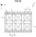
- FIG. 23 is a plan view corresponding to FIG. 18 .
- the fifth conductor 302 can be separate from the boundary of the unit resonator 40X.
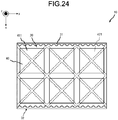
- FIG. 24 is a plan view corresponding to FIG. 18 .
- each of two pair conductors 30 can have a protruding portion that protrudes toward the other pair conductor 30 that is paired therewith.
- Such a resonator 10 can be formed, for example, by applying a metal paste to the base 20 having recessed portions and hardening the metal paste.
- FIG. 25 is a plan view corresponding to FIG. 18 .
- the base 20 can have recessed portions.
- the pair conductors 30 each have recessed portions that are recessed inward from an outer surface in the x direction.
- the pair conductors 30 each extend along a surface of the base 20.
- Such a resonator 10 can be formed, for example, by spraying a fine metal material on the base 20 having recessed portions.
- FIG. 26 is a plan view corresponding to FIG. 18 .
- the base 20 can have recessed portions.
- the pair conductors 30 each have recessed portions that are recessed inward from an outer surface in the x direction.
- the pair conductors 30 each extend along the recessed portions of the base 20.
- Such a resonator 10 can be produced, for example, by dividing a mother substrate along a row of through-hole conductors.
- Such pair conductors 30 can be referred to as castellated holes or the like.
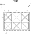
- FIG. 27 is a plan view corresponding to FIG. 18 .
- the base 20 can have recessed portions.
- the pair conductors 30 each have recessed portions that are recessed inward from an outer surface in the x direction.
- Such a resonator 10 can be produced, for example, by dividing a mother substrate along a row of through-hole conductors.
- Such pair conductors 30 can be referred to as castellated holes or the like.
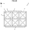
- FIG. 28 is a plan view corresponding to FIG. 18 .
- the pair conductors 30 may each have a smaller length in the x direction than that of the base 20.
- the configuration of the pair conductors 30 is not limited thereto.
- Two pair conductors 30 can have different configurations.
- one of the pair conductors 30 can include the fifth conductive layer 301 and the fifth conductor 302, and the other one of the pair conductors 30 can be a castellated hole.
- the third conductor 40 illustrated in each of FIGS. 1 to 28 is an example.
- the configuration of the third conductor 40 is not limited to the configurations illustrated in FIGS. 1 to 28 .
- the unit resonator 40X, the first unit resonator 41X, and the second unit resonator 42X are not limited to have a rectangular shape.
- the unit resonator 40X, the first unit resonator 41X, and the second unit resonator 42X can be referred to as the unit resonator 40X or the like.
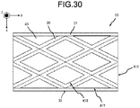
- the unit resonator 40X or the like may have a triangular shape as illustrated in FIG. 29A or may have a hexagonal shape as illustrated in FIG. 29B . As illustrated in FIG.
- each side of the unit resonator 40X or the like can extend in a direction different from the x direction and the y direction.
- the second conductive layer 42 can be positioned on the base 20 and the first conductive layer 41 can be positioned inside the base 20.
- the second conductive layer 42 can be positioned farther from the fourth conductor 50 than the first conductive layer 41 is.
- the third conductor 40 illustrated in each of FIGS. 1 to 30 is an example.
- the configuration of the third conductor 40 is not limited to the configurations illustrated in FIGS. 1 to 30 .
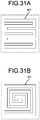
- the resonator including the third conductor 40 may be a line-type resonator 401.
- FIG. 31A illustrates a meander-line-type resonator 401.
- FIG. 31B illustrates a spiral-type resonator 401.
- the resonator including the third conductor 40 may be a slot-type resonator 402.
- the slot-type resonator 402 can include one or more seventh conductors 403 in an opening.
- the seventh conductor 403 in the opening has one end opened and the other end electrically connected to a conductor defining the opening.
- a unit slot illustrated in FIG. 31C five seventh conductors 403 are positioned in the opening.
- the unit slot has a shape corresponding to a meander line by the seventh conductors 403.
- one seventh conductor 403 is positioned in the opening.
- the unit slot has a shape corresponding to a spiral by the seventh conductor 403.
- the configuration of the resonator 10 illustrated in each of FIGS. 1 to 31 is an example.
- the configuration of the resonator 10 is not limited to the configurations illustrated in FIGS. 1 to 31 .
- the resonator 10 can include three or more pair conductors 30.
- one pair conductor 30 can face two pair conductors 30 in the x direction.
- the two pair conductors 30 are different in distance from the one pair conductor 30.
- the resonator 10 can include two pairs of pair conductors 30.
- the two pairs of pair conductors 30 can be different in regard to a distance between each pair and the lengths of each pair.
- the resonator 10 can include five or more first conductors.
- the unit structure 10X of the resonator 10 can be aligned with another unit structure 10X in the y direction.
- the unit structure 10X of the resonator 10 can be aligned with another unit structure 10X in the x direction without interposing the pair conductors 30 therebetween.
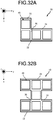
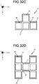
- FIGS. 32 to 34 are views each illustrating an example of the resonator 10. In the resonator 10 illustrated in FIGS. 32 to 34 , the unit resonator 40X of the unit structure 10X is shown as having a square shape, but the embodiments are not limited thereto.
- FIG. 35 is a plan view illustrating the xy plane viewed from the z direction.
- FIG. 36A is a cross-sectional view taken along line XXXVIa-XXXVIa illustrated in FIG. 35 .
- FIG. 36B is a cross-sectional view taken along line XXXVIb-XXXVIb illustrated in FIG. 35 .
- the first conductive layer 41 includes a half of a patch-type resonator as the first unit resonator 41X.
- the second conductive layer 42 includes a half of a patch-type resonator as the second unit resonator 42X.
- the unit resonator 40X includes one first divisional resonator 41Y and one second divisional resonator 42Y.
- the unit structure 10X includes the unit resonator 40X, and a portion of the base 20 and a portion of the fourth conductor 50 that overlap the unit resonator 40X in the Z direction.
- three unit resonators 40X are arranged in the x direction.
- the first unit conductor 411 and the second unit conductor 421 included in the three unit resonators 40X form one current path 401.
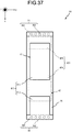
- FIG. 37 illustrates another example of the resonator 10 illustrated in FIG. 35 .
- the resonator 10 illustrated in FIG. 37 is longer in the x direction, as compared with the resonator 10 illustrated in FIG. 35 .
- the size of the resonator 10 is not limited to that of the resonator 10 illustrated in FIG. 37 and can be changed as appropriate.
- the length of the first connecting conductor 413 in the x direction is different from that of the first floating conductor 414.
- the length of the first connecting conductor 413 in the x direction is smaller than that of the first floating conductor 414.
- FIG. 38 illustrates another example of the resonator 10 illustrated in FIG.
- the length of the third conductor 40 in the x direction is different.
- the length of the first connecting conductor 413 in the x direction is larger than that of the first floating conductor 414.
- FIG. 39 illustrates another example of the resonator 10.
- FIG. 39 illustrates another example of the resonator 10 illustrated in FIG. 37 .
- a plurality of first unit conductors 411 arranged in the x direction and the second unit conductors 421 are capacitively coupled to each other.
- two current paths 401 can be arranged in the y direction, in which no current flows from one side to the other side.
- FIG. 40 illustrates another example of the resonator 10.
- FIG. 40 illustrates another example of the resonator 10 illustrated in FIG. 39 .
- the number of conductors connected to the first conductor 31 and the number of conductors connected to the second conductor 32 can be different from each other.
- one first connecting conductor 413 is capacitively coupled to two second floating conductors 424.
- two second connecting conductors 423 are capacitively coupled to one first floating conductor 414.
- the number of first unit conductors 411 can be different from the number of second unit conductors 421 that are capacitively coupled to the first unit conductor 411.
- FIG. 41 illustrates another example of the resonator 10 illustrated in FIG. 39 .
- the number of second unit conductors 421 that are capacitively coupled to a first end portion of the first unit conductor 411 in the x direction, and the number of second unit conductors 421 that are capacitively coupled to a second end portion of the first unit conductor 411 in the x direction can be different from each other.
- two first connecting conductors 413 are capacitively coupled to a first end portion of one second floating conductor 424 in the x direction and three second floating conductors 424 are capacitively coupled to a second end portion of the one second floating conductor 424.
- a plurality of conductors arranged in the y direction can have different lengths in the y direction.
- three first floating conductors 414 arranged in the y direction have different lengths in the y direction.
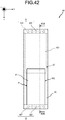
- FIG. 42 illustrates another example of the resonator 10.
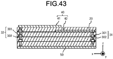
- FIG. 43 is a cross-sectional view taken along line XLIII-XLIII illustrated in FIG. 42 .
- the first conductive layer 41 includes a half of a patch-type resonator as the first unit resonator 41X.
- the second conductive layer 42 includes a half of a patch-type resonator as the second unit resonator 42X.
- the unit resonator 40X includes one first divisional resonator 41Y and one second divisional resonator 42Y.
- the unit structure 10X includes the unit resonator 40X, and a portion of the base 20 and a portion of the fourth conductor 50 that overlap the unit resonator 40X in the z direction. In the resonator 10 illustrated in FIG. 42 , one unit resonator 40X extends in the x direction.
- FIG. 44 illustrates another example of the resonator 10.
- FIG. 45 is a cross-sectional view taken along the line XLV-XLV illustrated in FIG. 44 .
- the third conductor 40 includes only the first connecting conductor 413.
- the first connecting conductor 413 faces the first conductor 31 in the xy plane.
- the first connecting conductor 413 is capacitively coupled to the first conductor 31.
- FIG. 46 illustrates another example of the resonator 10.
- FIG. 47 is a cross-sectional view taken along line XLVII-XLVII illustrated in FIG. 46 .
- the third conductor 40 includes the first conductive layer 41 and the second conductive layer 42.
- the first conductive layer 41 includes one first floating conductor 414.
- the second conductive layer 42 includes two second connecting conductors 423.
- the first conductive layer 41 faces the pair conductors 30 in the xy plane.
- the two second connecting conductors 423 overlap the one first floating conductor 414 in the z direction.
- the one first floating conductor 414 is capacitively coupled to the two second connecting conductors 423.
- FIG. 48 illustrates another example of the resonator 10.
- FIG. 49 is a cross-sectional view taken along line XLIX-XLIX illustrated in FIG. 48 .
- the third conductor 40 includes only the first floating conductor 414.
- the first floating conductor 414 faces the pair conductors 30 in the xy plane.
- the first connecting conductor 413 is capacitively coupled to the pair conductors 30.
- FIG. 50 illustrates another example of the resonator 10.
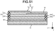
- FIG. 51 is a cross-sectional view taken along line LI-LI illustrated in FIG. 50 .
- the resonator 10 illustrated in FIGS. 50 and 51 is different from the resonator 10 illustrated in FIGS. 42 and 43 in regard to the configuration of the fourth conductor 50.
- the resonator 10 illustrated in FIGS. 50 and 51 includes the fourth conductor 50 and the reference potential layer 51.
- the reference potential layer 51 is electrically connected to the ground of the device including the resonator 10.
- the reference potential layer 51 faces the third conductor 40 while having the fourth conductor 50 interposed therebetween.
- the fourth conductor 50 is positioned between the third conductor 40 and the reference potential layer 51.
- An interval between the reference potential layer 51 and the fourth conductor 50 is smaller than an interval between the third conductor 40 and the fourth conductor 50.
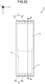
- FIG. 52 illustrates another example of the resonator 10.
- FIG. 53 is a cross-sectional view taken along line LIII-LIII illustrated in FIG. 52 .
- the resonator 10 includes the fourth conductor 50 and the reference potential layer 51.
- the reference potential layer 51 is electrically connected to the ground of the device including the resonator 10.
- the fourth conductor 50 includes a resonator.
- the fourth conductor 50 includes the third conductive layer 52 and the fourth conductive layer 53.
- the third conductive layer 52 and the fourth conductive layer 53 are capacitively coupled to each other.
- the third conductive layer 52 and the fourth conductive layer 53 face each other in the z direction.
- a distance between the third conductive layer 52 and the fourth conductive layer 53 is smaller than a distance between the fourth conductive layer 53 and the reference potential layer 51.
- the distance between the third conductive layer 52 and the fourth conductive layer 53 is smaller than a distance between the fourth conductor 50 and the reference potential layer 51.
- the third conductor 40 forms one conductive layer.
- FIG. 54 illustrates another example of the resonator 10 illustrated in FIG. 53 .
- the resonator 10 includes the third conductor 40, the fourth conductor 50, and the reference potential layer 51.
- the third conductor 40 includes the first conductive layer 41 and the second conductive layer 42.
- the first conductive layer 41 includes the first connecting conductor 413.
- the second conductive layer 42 includes the second connecting conductor 423.
- the first connecting conductor 413 is capacitively coupled to the second connecting conductor 423.
- the reference potential layer 51 is electrically connected to the ground of the device including the resonator 10.
- the fourth conductor 50 includes the third conductive layer 52 and the fourth conductive layer 53.
- the third conductive layer 52 and the fourth conductive layer 53 are capacitively coupled to each other.
- the third conductive layer 52 and the fourth conductive layer 53 face each other in the z direction.
- a distance between the third conductive layer 52 and the fourth conductive layer 53 is smaller than a distance between the fourth conductive layer 53 and the reference potential layer 51.
- the distance between the third conductive layer 52 and the fourth conductive layer 53 is smaller than a distance between the fourth conductor 50 and the reference potential layer 51.
- FIG. 55 illustrates another example of the resonator 10.
- FIG. 56A is a cross-sectional view taken along line LVIa-LVIa illustrated in FIG. 55 .
- FIG. 56B is a cross-sectional view taken along line LVIb-LVIb illustrated in FIG. 55 .
- the first conductive layer 41 includes four first floating conductors 414.
- the first conductive layer 41 illustrated in FIG. 55 does not include the first connecting conductor 413.
- the second conductive layer 42 includes six second connecting conductors 423 and three second floating conductors 424.
- Two second connecting conductors 423 are each capacitively coupled to two first floating conductors 414.
- One second floating conductor 424 is capacitively coupled to four first floating conductors 414.
- Two second floating conductors 424 are capacitively coupled to two first floating conductors 414.
- FIG. 57 is a view illustrating another example of the resonator illustrated in FIG. 55 .
- the resonator 10 of FIG. 57 is different from the resonator 10 illustrated in FIG. 55 in regard to the size of the second conductive layer 42.
- the length of the second floating conductor 424 in the x direction is smaller than the length of the second connecting conductor 423 in the x direction.
- FIG. 58 is a view illustrating another example of the resonator illustrated in FIG. 55 .
- the resonator 10 of FIG. 58 is different from the resonator 10 illustrated in FIG. 55 in regard to the size of the second conductive layer 42.
- a plurality of second unit conductors 421 have different first surface integrals.
- the plurality of second unit conductors 421 have different lengths in the x direction.
- the plurality of second unit conductors 421 have different lengths in the y direction.
- FIG. 58 the plurality of second unit conductors 421 have different lengths in the y direction.
- the plurality of second unit conductors 421 have different first surface integrals, lengths, and widths, but the embodiments are not limited thereto.
- some of the first surface integrals, lengths, and widths of the plurality of second unit conductors 421 can be different from each other.
- Some or all of the first surface integrals, lengths, and widths of the plurality of second unit conductors 421 can be identical to each other.
- Some or all of the first surface integrals, lengths, and widths of the plurality of second unit conductors 421 can be different from each other.
- Some or all of the first surface integrals, lengths, and widths of the plurality of second unit conductors 421 can be identical to each other.
- Some or all of the first surface integrals, lengths, and widths of some of the plurality of second unit conductors 421 can be identical to each other.
- a plurality of second connecting conductors 423 arranged in the y direction have different first surface integrals.
- the plurality of second connecting conductors 423 arranged in the y direction have different lengths in the x direction.
- the plurality of second connecting conductors 423 arranged in the y direction have different lengths in the y direction.
- the plurality of second connecting conductors 423 have different first surface integrals, lengths, and widths, but the embodiments are not limited thereto.
- some of the first surface integrals, lengths, and widths of the plurality of second connecting conductors 423 can be different from each other. Some or all of the first surface integrals, lengths, and widths of the plurality of second connecting conductors 423 can be identical to each other. Some or all of the first surface integrals, lengths, and widths of the plurality of second connecting conductors 423 can be different from each other. Some or all of the first surface integrals, lengths, and widths of the plurality of second connecting conductors 423 can be identical to each other. Some or all of the first surface integrals, lengths, and widths of some of the plurality of second connecting conductors 423 can be identical to each other.
- a plurality of second floating conductors 424 arranged in the y direction have different first surface integrals.
- the plurality of second floating conductors 424 arranged in the y direction have different lengths in the x direction.
- the plurality of second floating conductors 424 arranged in the y direction have different lengths in the y direction.
- the plurality of second floating conductors 424 have different first surface integrals, lengths, and widths, but the embodiments are not limited thereto.
- some of the first surface integrals, lengths, and widths of the plurality of second floating conductors 424 can be different from each other. Some or all of the first surface integrals, lengths, and widths of the plurality of second floating conductors 424 can be identical to each other. Some or all of the first surface integrals, lengths, and widths of the plurality of second floating conductors 424 can be different from each other. Some or all of the first surface integrals, lengths, and widths of the plurality of second floating conductors 424 can be identical to each other. Some or all of the first surface integrals, lengths, and widths of some of the plurality of second floating conductors 424 can be identical to each other.
- FIG. 59 is a view illustrating another example of the resonator 10 illustrated in FIG. 57 .
- the resonator 10 of FIG. 59 is different from the resonator 10 illustrated in FIG. 57 in regard to an interval between the first unit conductors 411 in the y direction.
- the interval between the first unit conductors 411 in the y direction is smaller than an interval between the first unit conductors 411 in the x direction.
- the pair conductors 30 can function as electric conductors, a current flows in the x direction.
- a current flowing through the third conductor 40 in the y direction can be ignored.
- the interval between the first unit conductors 411 in the y direction may be smaller than the interval between the first unit conductors 411 in the x direction. By decreasing the interval between the first unit conductors 411 in the y direction, the surface integral of the first unit conductor 411 can be increased.
- FIGS. 60 to 62 are views each illustrating another example of the resonator 10. These resonators 10 each include the impedance element 45.
- a unit conductor to which the impedance element 45 is connected is not limited to the examples illustrated in FIGS. 60 to 62 .
- the impedance element 45 illustrated in FIGS. 60 to 62 can be partially omitted.
- the impedance element 45 can have a capacitance characteristic.
- the impedance element 45 can have an inductance characteristic.
- the impedance element 45 can be a mechanical or electrical variable element.
- the impedance element 45 can connect two different conductors in one layer to each other.
- An antenna has at least one of a function of radiating electromagnetic waves or a function of receiving electromagnetic waves.
- Antennas of the present disclosure include, but are not limited to, a first antenna 60 and a second antenna 70.
- the first antenna 60 includes the base 20, the pair conductors 30, the third conductor 40, the fourth conductor 50, and a first feeding line 61.
- the first antenna 60 includes a third base 24 positioned on the base 20.
- the third base 24 can have a different composition than the base 20.
- the third base 24 can be positioned over the third conductor 40.
- FIGS. 63 to 76 are views each illustrating the first antenna 60 as an example of embodiments.
- the first feeding line 61 feeds power to at least one of the resonators arranged periodically as artificial magnetic conductors.
- the first antenna 60 can include a plurality of first feeding lines.
- the first feeding line 61 can be electromagnetically connected to any one of the resonators arranged periodically as artificial magnetic conductors.
- the first feeding line 61 can be electromagnetically connected to any one of a pair of conductors that is seen as electric conductors for the resonators that are periodically arranged as artificial magnetic conductors.
- the first feeding line 61 feeds power to at least one of the first conductor 31, the second conductor 32, or the third conductor 40.
- the first antenna 60 can include a plurality of first feeding lines.
- the first feeding line 61 can be electromagnetically connected to any one of the first conductor 31, the second conductor 32, or the third conductor 40.
- the first feeding line 61 can be electromagnetically connected to any one of the first conductor 31, the second conductor 32, the third conductor 40, or the fourth conductor 50.
- the first feeding line 61 is electrically connected to any one of the fifth conductive layer 301 or the fifth conductor 302 of the pair conductors 30. A portion of the first feeding line 61 can be integrated with the fifth conductive layer 301.
- the first feeding line 61 can be electromagnetically connected to the third conductor 40.
- the first feeding line 61 is electromagnetically connected to one of the first unit resonators 41X.
- the first feeding line 61 is electromagnetically connected to one of the second unit resonators 42X.
- the first feeding line 61 is electromagnetically connected to a unit conductor of the third conductor 40 at a point different from the center in the x direction.
- the first feeding line 61 supplies power to at least one resonator included in the third conductor 40 in embodiments.
- the first feeding line 61 feeds power from at least one resonator included in the third conductor 40 to the outside.
- At least a portion of the first feeding line 61 can be positioned inside the base 20.
- the first feeding line 61 can be exposed to the outside from any of two zx planes, two yz planes, or two xy planes of the base 20.
- the first feeding line 61 can be in contact with the third conductor 40 from forward and rearward in the z direction.
- the fourth conductor 50 can be omitted in the vicinity of the first feeding line 61.
- the first feeding line 61 can be electromagnetically connected to the third conductor 40 through an opening of the fourth conductor 50.
- the first conductive layer 41 can be omitted in the vicinity of the first feeding line 61.
- the first feeding line 61 can be connected to the second conductive layer 42 through an opening of the first conductive layer 41.
- the first feeding line 61 can be in contact with the third conductor 40 along the xy plane.
- the pair conductors 30 can be omitted in the vicinity of the first feeding line 61.
- the first feeding line 61 can be connected to the third conductor 40 through an opening of the pair conductors 30.
- the first feeding line 61 is connected to a unit conductor of the third conductor 40 at a point away from a central portion of the unit conductor.
- FIG. 63 is a plan view illustrating the xy plane of the first antenna 60 viewed from the z direction.
- FIG. 64 is a cross-sectional view taken along line LXIV-LXIV illustrated in FIG. 63 .
- the first antenna 60 illustrated in FIGS. 63 and 64 includes the third base 24 positioned over the third conductor 40.
- the third base 24 has an opening on the first conductive layer 41.
- the first feeding line 61 is electrically connected to the first conductive layer 41 through the opening of the third base 24.
- FIG. 65 is a plan view illustrating the xy plane of the first antenna 60 viewed from the z direction.
- FIG. 66 is a cross-sectional view taken along line LXVI-LXVI illustrated in FIG. 65 .
- a portion of the first feeding line 61 is positioned on the base 20.
- the first feeding line 61 can be connected to the third conductor 40 in the xy plane.
- the first feeding line 61 can be connected to the first conductive layer 41 in the xy plane.
- the first feeding line 61 can be connected to the second conductive layer 42 in the xy plane.
- FIG. 67 is a plan view illustrating the xy plane of the first antenna 60 viewed from the z direction.
- FIG. 68 is a cross-sectional view taken along line LXVIII-LXVIII illustrated in FIG. 67 .
- the first feeding line 61 is positioned inside the base 20.
- the first feeding line 61 can be connected to the third conductor 40 from rearward in the z direction.
- the fourth conductor 50 can have an opening.
- the fourth conductor 50 can have the opening at a position where the fourth conductor 50 overlaps the third conductor 40 in the z direction.
- the first feeding line 61 can be exposed to the outside of the base 20 through the opening.
- FIG. 69 is a cross-sectional view of the first antenna 60 taken along the yz plane viewed from the x direction.
- the pair conductors 30 can have an opening.
- the first feeding line 61 can be exposed to the outside of the base 20 through the opening.
- Electromagnetic waves radiated by the first antenna 60 includes polarization components in the x direction more than that in the y direction in the first plane.
- the polarization components in the x direction are less attenuated than horizontal polarization components when a metal plate approaches the fourth conductor 50 in the z direction.
- the first antenna 60 can maintain radiation efficiency when the metal plate approaches from the outside.
- FIG. 70 illustrates another example of the first antenna 60.
- FIG. 71 is a cross-sectional view taken along line LXXI-LXXI illustrated in FIG. 70 .
- FIG. 72 illustrates another example of the first antenna 60.
- FIG. 73 is a cross-sectional view taken along the line LXXIII-LXXIII illustrated in FIG. 72 .
- FIG. 74 illustrates another example of the first antenna 60.
- FIG. 75A is a cross-sectional view taken along line LXXVa-LXXVa illustrated in FIG. 74 .
- FIG. 75B is a cross-sectional view taken along line LXXVb-LXXVb illustrated in FIG. 74 .
- FIG. 76 illustrates another example of the first antenna 60.
- the first antenna 60 illustrated in FIG. 76 includes the impedance element 45.
- the operating frequency of the first antenna 60 can be changed by the impedance element 45.
- the first antenna 60 includes a first feeding conductor 415 connected to the first feeding line 61 and a first unit conductor 411 that is not connected to the first feeding line 61. Impedance matching is changed when the impedance element 45 is connected to the first feeding conductor 415 and another conductor.
- the impedance matching of the first antenna 60 can be adjusted by connecting the first feeding conductor 415 and another conductor with the impedance element 45.
- the impedance element 45 can be inserted between the first feeding conductor 415 and another conductor in order to adjust the impedance matching.
- the impedance element 45 can be inserted between two first unit conductors 411 that are not connected to the first feeding line 61 in order to adjust the operating frequency.
- the impedance element 45 can be inserted between one of the pair conductors 30 and the first unit conductor 411 that is not connected to the first feeding line 61 in order to adjust the operating frequency.
- the second antenna 70 includes the base 20, the pair conductors 30, the third conductor 40, the fourth conductor 50, a second feeding layer 71, and a second feeding line 72.
- the third conductor 40 is positioned inside the base 20.
- the second antenna 70 includes the third base 24 positioned on the base 20.
- the third base 24 can have a different composition than the base 20.
- the third base 24 can be positioned over the third conductor 40.
- the third base 24 can be positioned on the second feeding layer 71.
- the second feeding layer 71 is positioned above the third conductor 40 with a space therebetween.
- the base 20 or the third base 24 can be positioned between the second feeding layer 71 and the third conductor 40.
- the second feeding layer 71 includes a line-type resonator, a patch-type resonator, or a slot-type resonator.
- the second feeding layer 71 can be referred to as an antenna element.
- the second feeding layer 71 can be electromagnetically coupled to the third conductor 40.
- the resonant frequency of the second feeding layer 71 is changed from a single resonant frequency by electromagnetic coupling with the third conductor 40.
- the second feeding layer 71 receives power transmitted from the second feeding line 72 and resonates with the third conductor 40.
- the second feeding layer 71 receives power transmitted from the second feeding line 72 and resonates with the third conductor 40 and the third conductor.
- the second feeding line 72 is electrically connected to the second feeding layer 71. In embodiments, the second feeding line 72 transmits power to the second feeding layer 71. In embodiments, the second feeding line 72 transmits power from the second feeding layer 71 to the outside.
- FIG. 77 is a plan view illustrating the xy plane of the second antenna 70 viewed from the z direction.
- FIG. 78 is a cross-sectional view taken along line LXXVIII-LXXVIII illustrated in FIG. 77 .
- the third conductor 40 is positioned inside the base 20.
- the second feeding layer 71 is positioned on the base 20.
- the second feeding layer 71 is positioned in such a manner as to overlap the unit structure 10X in the z direction.
- the second feeding line 72 is positioned on the base 20.
- the second feeding line 72 is electromagnetically connected to the second feeding layer 71 in the xy plane.
- a wireless communication module of the present disclosure includes a wireless communication module 80 as an example of embodiments.
- FIG. 79 is a block structural diagram of the wireless communication module 80.
- FIG. 80 is a schematic configuration diagram of the wireless communication module 80.
- the wireless communication module 80 includes the first antenna 60, a circuit board 81, and an RF module 82.
- the wireless communication module 80 can include the second antenna 70 instead of the first antenna 60.
- the first antenna 60 is positioned on the circuit board 81.
- the first feeding line 61 of the first antenna 60 is electromagnetically connected to the RF module 82 via the circuit board 81.
- the fourth conductor 50 of the first antenna 60 is electromagnetically connected to a ground conductor 811 of the circuit board 81.
- the ground conductor 811 can extend in the xy plane.
- the ground conductor 811 has a surface integral larger than that of the fourth conductor 50 in the xy plane.
- the ground conductor 811 is longer than the fourth conductor 50 in the y direction.
- the ground conductor 811 is longer than the fourth conductor 50 in the x direction.
- the first antenna 60 can be positioned closer to an end side than to the center of the ground conductor 811 in the y direction.
- the center of the first antenna 60 can be different from the center of the ground conductor 811 in the xy plane.
- the center of the first antenna 60 can be different from the centers of the first conductive layer 41 and the second conductive layer 42.
- a point where the first feeding line 61 is connected to the third conductor 40 can be different from the center of the ground conductor 811 in the xy plane.
- the first antenna 60 In the first antenna 60, the first current and the second current loop through the pair conductors 30. Since the first antenna 60 is positioned closer to the end side in the y direction than to the center of the ground conductor 811, the second current flowing through the ground conductor 811 becomes asymmetric. When the second current flowing through the ground conductor 811 becomes asymmetric, in an antenna structure including the first antenna 60 and the ground conductor 811, a polarization component of radiation waves in the x direction is increased. By increasing the polarization component of the radiation waves in the x direction, a total radiation efficiency of the radiation wave can be improved.
- the RF module 82 can be operated in such a manner as to control power supplied to the first antenna 60.
- the RF module 82 modulates a baseband signal and supplies the modulated baseband signal to the first antenna 60.
- the RF module 82 can be operated in such a manner as to modulate an electric signal received by the first antenna 60 into a baseband signal.
- a change in resonant frequency of the first antenna 60 due to a conductor on the circuit board 81 side is small.
- the wireless communication module 80 can reduce an influence of an external environment by including the first antenna 60.
- the first antenna 60 can be integrated with the circuit board 81.
- the fourth conductor 50 and the ground conductor 811 are integrated with each other.
- a wireless communication device of the present disclosure includes a wireless communication device 90 as an example of embodiments.
- FIG. 81 is a block structural diagram of the wireless communication device 90.
- FIG. 82 is a plan view of the wireless communication device 90. The configuration of the wireless communication device 90 illustrated in FIG. 82 is partially omitted.
- FIG. 83 is a cross-sectional view of the wireless communication device 90. The configuration of the wireless communication device 90 illustrated in FIG. 83 is partially omitted.
- the wireless communication device 90 includes the wireless communication module 80, a battery 91, a sensor 92, a memory 93, a controller 94, a first case 95, and a second case 96.
- the wireless communication module 80 of the wireless communication device 90 includes the first antenna 60, and can include the second antenna 70.
- FIG. 84 is one of other embodiments of the wireless communication device 90.
- the first antenna 60 included in the wireless communication device 90 can include the reference potential layer 51.
- the battery 91 supplies power to the wireless communication module 80.
- the battery 91 can supply power to at least one of the sensor 92, the memory 93, or the controller 94.
- the battery 91 can include at least one of a primary battery or a secondary battery.
- a negative electrode of the battery 91 is electrically connected to a ground terminal of the circuit board 81.
- the negative electrode of the battery 91 is electrically connected to the fourth conductor 50 of the first antenna 60.
- Examples of the sensor 92 may include a speed sensor, a vibration sensor, an acceleration sensor, a gyro sensor, a rotation angle sensor, an angular velocity sensor, a geomagnetic sensor, a magnet sensor, a temperature sensor, a humidity sensor, an atmospheric pressure sensor, an optical sensor, an illuminance sensor, a UV sensor, a gas sensor, a gas concentration sensor, an atmosphere sensor, a level sensor, an odor sensor, a pressure sensor, an air pressure sensor, a contact sensor, a wind sensor, an infrared sensor, a motion sensor, a displacement sensor, an image sensor, a weight sensor, a smoke sensor, a leakage sensor, a vital sensor, a state-of-charge (SOC) sensor, an ultrasonic sensor, and a global positioning system (GPS) signal receiving device.
- GPS global positioning system
- Examples of the memory 93 can include a semiconductor memory.
- the memory 93 can function as a work memory of the controller 94.
- the memory 93 can be included in the controller 94.
- the memory 93 stores a program describing processing for realizing each function of the wireless communication device 90, information used for processing in the wireless communication device 90, and the like.
- Examples of the controller 94 can include a processor.
- the controller 94 may include one or more processors.
- the processor may be a general-purpose processor that loads a specific program and executes a specific function, or a dedicated processor that is specialized for specific processing.
- the dedicated processor may include an application specific integrated circuit (IC).
- the application specific IC is also referred to as ASIC.
- the processor may include a programmable logic device.
- the programmable logic device is also called PLD.
- the PLD may include a field-programmable gate array (FPGA).
- the controller 94 may be any one of a system on a chip (SoC) in which one or more processors cooperate, or a system in a package (SiP).
- SoC system on a chip
- SiP system in a package
- the controller 94 may store, in the memory 93, various information, a program for operating each component of the wireless communication device 90, or the like.
- the controller 94 can be operated in such a manner as to generate a transmission signal to be transmitted from the wireless communication device 90.
- the controller 94 may obtain measurement data from the sensor 92, for example.
- the controller 94 may generate a transmission signal according to the measurement data.
- the controller 94 can be operated in such a manner as to transmit a baseband signal to the RF module 82 of the wireless communication module 80.
- the first case 95 and the second case 96 protect other devices of the wireless communication device 90.
- the first case 95 can extend in the xy plane.
- the first case 95 supports other devices.
- the first case 95 can support the wireless communication module 80.
- the wireless communication module 80 is positioned on an upper surface 95A of the first case 95.
- the first case 95 can support the battery 91.
- the battery 91 is positioned on the upper surface 95A of the first case 95.
- the wireless communication module 80 and the battery 91 are arranged in the x direction on the upper surface 95A of the first case 95.
- the first conductor 31 is positioned between the battery 91 and the third conductor 40.
- the battery 91 is positioned on the opposite side of the pair conductors 30 from the third conductor 40.
- the second case 96 can cover other devices.
- the second case 96 has an under surface 96A positioned to face the first antenna 60 in the z direction.
- the under surface 96A extends along the xy plane.
- the under surface 96A is not limited to being a flat surface and can be a rugged surface.
- the second case 96 can include an eighth conductor 961.
- the eighth conductor 961 is positioned on at least one of an inner portion, the outside, or the inside of the second case 96.
- the eighth conductor 961 is positioned on at least one of an upper surface or a side surface of the second case 96.
- the eighth conductor 961 faces the first antenna 60.
- a first body 9611 of the eighth conductor 961 faces the first antenna 60 in the z direction.
- the eighth conductor 961 can include, in addition to the first body 9611, at least one of a second body facing the first antenna 60 in the x direction or a third body facing the first antenna in the y direction.
- a portion of the eighth conductor 961 faces the battery 91.
- the eighth conductor 961 can include a first extra-body 9612 that extends outward from the first conductor 31 in the x direction.
- the eighth conductor 961 can include a second extra-body 9613 that extends outward from the second conductor 32 in the x direction.
- the first extra-body 9612 can be electrically connected to the first body 9611.
- the second extra-body 9613 can be electrically connected to the first body 9611.
- the first extra-body 9612 of the eighth conductor 961 faces the battery 91 in the z direction.
- the eighth conductor 961 can be capacitively coupled to the battery 91. A capacitance can be formed between the eighth conductor 961 and the battery 91.
- the eighth conductor 961 is separated from the third conductor 40 of the first antenna 60.
- the eighth conductor 961 is not electrically connected to each conductor of the first antenna 60.
- the eighth conductor 961 can be separated from the first antenna 60.
- the eighth conductor 961 can be electromagnetically coupled to any conductor of the first antenna 60.
- the first body 9611 of the eighth conductor 961 can be electromagnetically coupled to the first antenna 60.
- the first body 9611 can overlap the third conductor 40 when viewed in plan from the z direction. Since the first body 9611 overlaps the third conductor 40, propagation due to electromagnetic coupling can be increased. Electromagnetic coupling between the eighth conductor 961 and the third conductor 40 can cause a mutual inductance.
- the eighth conductor 961 extends in the x direction.
- the eighth conductor 961 extends along the xy plane.
- the length of the eighth conductor 961 is larger than the length of the first antenna 60 in the x direction.
- the length of the eighth conductor 961 in the x direction is larger than the length of the first antenna 60 in the x direction.
- the length of the eighth conductor 961 can be larger than 1/2 of the operating wavelength ⁇ of the wireless communication device 90.
- the eighth conductor 961 can include a portion extending in the y direction.
- the eighth conductor 961 can be bent in the xy plane.
- the eighth conductor 961 can include a portion extending in the z direction.
- the eighth conductor 961 can be bent from the xy plane to the yz plane or the zx plane.
- the wireless communication device 90 including the eighth conductor 961 can function as a third antenna 97 by electromagnetically coupling the first antenna 60 and the eighth conductor 961 to each other.
- the operating frequency f c of the third antenna 97 may be different from the resonant frequency of the first antenna 60 alone.
- the operating frequency f c of the third antenna 97 may be closer to the resonant frequency of the first antenna 60 than to the resonant frequency of the eighth conductor 961 alone.
- the operating frequency f c of the third antenna 97 can be within a resonant frequency band of the first antenna 60.
- the operating frequency f c of the third antenna 97 can be out of a resonant frequency band of the eighth conductor 961 alone.
- the eighth conductor 961 can be integrated with the first antenna 60.
- the configuration of the wireless communication device 90 is partially omitted.
- the second case 96 does not have to include the eighth conductor 961.
- the eighth conductor 961 is capacitively coupled to the third conductor 40.
- the eighth conductor 961 is electromagnetically coupled to the fourth conductor 50. Since the third antenna 97 includes the first extra-body 9612 and the second extra-body 9613 of the eighth conductor in the air, a gain is improved as compared with the first antenna 60.
- the wireless communication device 90 can be positioned on various objects.
- the wireless communication device 90 can be positioned on an electrical conductive body 99.
- FIG. 86 is a plan view illustrating an embodiment of the wireless communication device 90.
- the electrical conductive body 99 is a conductor that conducts electricity.
- the material of the electrical conductive body 99 is a metal, a highly doped semiconductor, a conductive plastic, or a liquid containing ions.
- the electrical conductive body 99 can include a non-conductive layer that does not conduct electricity and is positioned on a surface of the electrical conductive body 99.
- a portion that conducts electricity and the non-conductive layer can contain a common chemical element.
- the electrical conductive body 99 containing aluminum can include a non-conductive layer containing aluminum oxide and positioned on the surface thereof.
- the portion that conducts electricity and the non-conductive layer can each include a different chemical element.
- the shape of the electrical conductive body 99 is not limited to a flat plate shape, and can be a three-dimensional shape such as a box shape.
- the three-dimensional shape of the electrical conductive body 99 is a rectangular parallelepiped or a cylinder.
- the three-dimensional shape can be a partially depressed shape, a partially penetrated shape, or a partially protruding shape.
- the electrical conductive body 99 can have a torus shape.
- the electrical conductive body 99 has an upper surface 99A on which the wireless communication device 90 can be placed.
- the upper surface 99A can extend over the entire surface of the electrical conductive body 99.
- the upper surface 99A can be a portion of the electrical conductive body 99.
- the upper surface 99A can have a surface integral larger than that of the wireless communication device 90.
- the wireless communication device 90 can be placed on the upper surface 99A of the electrical conductive body 99.
- the upper surface 99A can have a surface integral smaller than the wireless communication device 90.
- the wireless communication device 90 can be partially placed on the upper surface 99A of the electrical conductive body 99.
- the wireless communication device 90 can be placed on the upper surface 99A of the electrical conductive body 99 in various orientations. The orientation of the wireless communication device 90 can be arbitrary.
- the wireless communication device 90 can be appropriately fixed on the upper surface 99A of the electrical conductive body 99 by using a fixture.
- the fixture includes one used for surface-fixation, such as a double-sided tape or an adhesive.
- the fixture includes one used for point-fixation, such as a screw or a nail.
- the upper surface 99A of the electrical conductive body 99 can have a portion extending in a j direction.
- the length of the portion in the j direction is larger than the length of the portion in a k direction, the portion extending in the j direction.
- the j direction and the k direction are orthogonal to each other.
- the j direction is a direction in which the electrical conductive body 99 extends longitudinally.
- the k direction is a direction in which the electrical conductive body 99 has a length smaller than that in the j direction.
- the wireless communication device 90 can be placed on the upper surface 99A in such a manner that the x direction is along the j direction.
- the wireless communication device 90 can be placed on the upper surface 99A of the electrical conductive body 99 in such a manner as to be aligned with the x direction in which the first conductor 31 and the second conductor 32 are arranged.
- the first antenna 60 can be electromagnetically coupled to the electrical conductive body 99.
- the second current flows in the x direction.
- a current is induced in the electrical conductive body 99 electromagnetically coupled to the first antenna 60 by the second current.
- An angle of the x direction with respect to the j direction can be 45 degrees or less.
- the ground conductor 811 of the wireless communication device 90 is separated from the electrical conductive body 99.
- the ground conductor 811 is separated from the electrical conductive body 99.
- the wireless communication device 90 can be placed on the upper surface 99A in such a manner that a direction along a longer side of the upper surface 99A is aligned with the x direction in which the first conductor 31 and the second conductor 32 are arranged.
- the upper surface 99A can be a rectangular surface, a rhombus-shaped surface, or a circular surface.
- the electrical conductive body 99 can have a rhombus-shaped surface. This rhombus-shaped surface can be the upper surface 99A on which the wireless communication device 90 is placed.
- the wireless communication device 90 can be placed on the upper surface 99A in such a manner that a direction along a longer diagonal line of the upper surface 99A is aligned with the x direction in which the first conductor 31 and the second conductor 32 are arranged.
- the upper surface 99A is not limited to be a flat surface.
- the upper surface 99A can be a rugged surface.
- the upper surface 99A can include a curved surface.
- the curved surface includes a ruled surface.
- the curved surface includes a cylindrical surface.
- the electrical conductive body 99 extends in the xy plane.
- the length of the electrical conductive body 99 in the x direction can be larger than the length of the electrical conductive body 99 in the y direction.
- the length of the electrical conductive body 99 in the y direction can be smaller than a half of a wavelength ⁇ c at the operating frequency f c of the third antenna 97.
- the wireless communication device 90 can be positioned on an electrical conductive body 99.
- the electrical conductive body 99 is positioned away from the fourth conductor 50 in the z direction.
- the length of the electrical conductive body 99 in the x direction is larger than that of the fourth conductor 50.
- the surface integral of the electrical conductive body 99 in the xy plane is larger than that of the fourth conductor 50.
- the electrical conductive body 99 is positioned away from the ground conductor 811 in the z direction.
- the length of the electrical conductive body 99 in the x direction is larger than that of the ground conductor 811.
- the surface integral of the electrical conductive body 99 in the xy plane is larger than that of the ground conductor 811.
- the wireless communication device 90 can be placed on the electrical conductive body 99 in an orientation in which the x direction in which the first conductor 31 and the second conductor 32 are arranged is aligned with the direction in which the electrical conductive body 99 extends longitudinally.
- the wireless communication device 90 can be placed on the electrical conductive body 99 in an orientation in which a direction in which the current of the first antenna 60 flows in the xy plane is aligned with the direction in which the electrical conductive body 99 extends longitudinally.
- a change in resonant frequency of the first antenna 60 due to a conductor on the circuit board 81 side is small. Since the wireless communication device 90 includes the first antenna 60, an influence of an external environment can be reduced.
- the ground conductor 811 is capacitively coupled to the electrical conductive body 99. Since the wireless communication device 90 includes a portion of the electrical conductive body 99 that extends outward from the third antenna 97, a gain is increased as compared with the first antenna 60.
- FIG. 87 is a schematic circuit of a resonance structure formed in the air.
- FIG. 88 is a schematic circuit of a resonance structure formed on the electrical conductive body 99.
- L3 represents the inductance of the resonator 10
- L8 represents the inductance of the eighth conductor 961
- L9 represents the inductance of the electrical conductive body 99
- M represents the mutual inductance of L3 and L8.
- C3 represents the capacitance of the third conductor 40
- C4 represents the capacitance of the fourth conductor 50
- C8 represents the capacitance of the eighth conductor 961
- C8B represents the capacitance of the eighth conductor 961 and the battery 91
- C9 represents the capacitance of the electrical conductive body 99 and the ground conductor 811.
- R3 represents the radiation resistance of the resonator 10
- R8 represents the radiation resistance of the eighth conductor 961.
- the operating frequency of the resonator 10 is lower than the resonant frequency of the eighth conductor.
- the ground conductor 811 functions as a chassis ground in the air.
- the fourth conductor 50 is capacitively coupled to the electrical conductive body 99.
- the electrical conductive body 99 functions as a substantial chassis ground.
- the wireless communication device 90 includes the eighth conductor 961.
- the eighth conductor 961 is electromagnetically coupled to the first antenna 60 and capacitively coupled to the fourth conductor 50.
- the wireless communication device 90 can increase the operating frequency when placed on the electrical conductive body 99 from the air by increasing the capacitance C8B caused by the capacitive coupling.
- the wireless communication device 90 can reduce the operating frequency when placed on the electrical conductive body 99 from the air by increasing the mutual inductance M caused by the electromagnetic coupling.
- the wireless communication device 90 can adjust the change in operating frequency when placed on the electrical conductive body 99 from the air by changing a balance between the capacitance C8B and the mutual inductance M.
- the wireless communication device 90 can reduce the change in operating frequency when placed on the electrical conductive body 99 from the air by changing the balance between the capacitance C8B and the mutual inductance M.
- the wireless communication device 90 includes the eighth conductor 961 that is electromagnetically coupled to the third conductor 40 and capacitively coupled to the fourth conductor 50. By including the eighth conductor 961, the wireless communication device 90 can adjust the change in operating frequency when placed on the electrical conductive body 99 from the air. By including the eighth conductor 961, the wireless communication device 90 can reduce the change in operating frequency when placed on the electrical conductive body 99 from the air.
- the ground conductor 811 functions as a chassis ground in the air.
- the electrical conductive body 99 functions as a substantial chassis ground on the electrical conductive body 99.
- the resonance structure including the resonator 10 can oscillate even when the chassis ground is changed. This corresponds to the fact that the resonator 10 including the reference potential layer 51 and the resonator 10 that does not include the reference potential layer 51 can oscillate.
- FIG. 89 is a perspective view illustrating an embodiment of an array antenna 1.
- FIG. 90 is a cross-sectional view of an antenna element 100 and an antenna board 200 taken along line L1-L1 illustrated in FIG. 89 .
- a fourth axis is referred to as an X direction.
- a fifth axis is referred to as a Y direction.
- an eighth axis is referred to as a Z direction.
- An XYZ coordinate system illustrated in FIG. 89 or the like may be independent of an xyz axis coordinate system illustrated in FIG. 1 or the like.
- the XYZ coordinate system illustrated in FIG. 89 or the like may correspond to the xyz axis coordinate system illustrated in FIG. 1 or the like.
- the fourth axis, that is, the X direction may be a direction along the x direction, which is the first axis, or the y direction, which is the third axis.
- the array antenna 1 illustrated in FIG. 89 may be positioned on a circuit board 2.
- the array antenna 1 can be connected to an integrated circuit 3 via the circuit board 2.
- the integrated circuit 3 may be a radio frequency integrated circuit (RFIC).
- the array antenna 1 may be directly connected to the integrated circuit 3 without interposing the circuit board 2 therebetween. In other words, the array antenna 1 does not have to be positioned on the circuit board 2.
- the array antenna 1 includes a plurality of antenna elements 100 and the antenna board 200.
- the plurality of antenna elements 100 are arranged in a grid pattern in the array antenna 1.
- the plurality of antenna elements 100 can be arranged in a square grid, an oblique grid, a rectangular grid, a triangular grid, or a hexagonal grid.
- the plurality of antenna elements 100 can be arranged in a grid pattern along the X direction and Y direction, as illustrated in FIG. 89 .
- the plurality of antenna elements 100 may be arranged linearly. In this case, the plurality of antenna elements 100 can be arranged along the X direction (or Y direction).
- the plurality of antenna elements 100 may be integrated with the antenna board 200.
- the antenna element 100 includes a fourth antenna 110 and a filter 120. Electromagnetic waves received by the fourth antenna 110 are supplied as an electric signal to the integrated circuit 3 illustrated in FIG. 89 via the filter 120. The electric signal output by the integrated circuit 3 illustrated in FIG. 89 is radiated as electromagnetic waves by the fourth antenna 110 via the filter 120 illustrated in FIG. 90 .
- the fourth antenna 110 includes the first conductor 31, the second conductor 32, the third conductor 40, the fourth conductor 50, and a third feeding line 111 electrically connected to the third conductor 40.
- the filter 120 is electrically connected to the third feeding line 111 of the fourth antenna 110. As illustrated in FIG. 90 , the filter 120 is positioned in such a manner as to overlap the fourth conductor 50 in the Z direction.
- the filter 120 may be formed in the antenna board 200. An arbitrary structure may be adopted for the filter 120 according to a frequency band of electromagnetic waves transmitted and received by the array antenna 1, or the like.
- the filter 120 may be a laminated waveguide type filter.
- the filter 120 can include a conductor 121, a wire 122, conductors 123, 124, and 125, and conductors 126 and 127.
- the filter 120 may include any number of laminated waveguide type filters.
- the conductor 121 may be formed of the same material as the fourth conductor 50.
- the conductor 121 and the fourth conductor 50 may be shared. That is, the conductor 121 and the fourth conductor 50 may be integrated with each other.
- the conductor 121 may be a separate member independent of the fourth conductor 50. In a case where the conductor 121 is a separate member independent of the fourth conductor 50, the conductor 121 overlaps the fourth conductor 50.
- the wire 122 may be formed of any metal material.
- the wire 122 may be formed as a microstrip line.
- the wire 122 may be electrically connected to the circuit board 2 illustrated in FIG. 89 .
- the wire 122 can be electrically connected to the integrated circuit 3 via the circuit board 2 illustrated in FIG. 89 .
- the wire 122 can be electrically directly connected to the integrated circuit 3.
- the conductors 123 to 125 function as a part of a laminated waveguide.
- the conductors 123 to 125 may be formed of any metal material.
- the conductors 123 to 125 each include an opening portion.
- the conductors 123 to 125 are arranged in such a manner that the opening portions face each other in the Z direction. The electric signal is sent and received by electromagnetic coupling through the opening portions.
- the conductor 126 extends along the Z direction near one end portion of the filter 120.
- a plurality of conductors 126 arranged in the y direction are electrically connected via the conductor 125 extending in the y direction.
- the conductor 127 extends along the Z direction near the other end portion of the filter 120.
- a plurality of conductors 126 arranged in the y direction are electrically connected via the conductor 125 extending in the y direction.
- the antenna board 200 illustrated in FIG. 90 can be a dielectric board. Similar to the base 20 illustrated in FIG. 1 , the antenna board 200 can include any one of a ceramic material or a resin material as a composition. The antenna element 100 is positioned on the antenna board 200.
- FIG. 91 is a perspective view illustrating an embodiment of an array antenna 1A.
- FIG. 92 is a cross-sectional view of an antenna element 101 and an antenna board 210 taken along line L2-L2 illustrated in FIG. 91 .
- the array antenna 1A illustrated in FIG. 91 can be electrically connected to the integrated circuit 3 via the circuit board 2.
- the array antenna 1A includes a plurality of antenna elements 101 and the antenna board 210.
- the antenna element 101 includes the fourth antenna 110 and the filter 130.
- the filter 130 is electrically connected to the third feeding line 111 of the fourth antenna 110. As illustrated in FIG. 92 , the filter 130 is positioned in such a manner as to overlap the fourth conductor 50 in the Z direction.
- the filter 130 may be formed in a board part 211 of the antenna board 210. An arbitrary structure may be adopted for the filter 130 according to a frequency band of electromagnetic waves transmitted and received by the array antenna 1A, or the like.
- the filter 130 may be a dielectric filter. As illustrated in FIG.
- the filter 130 can include a conductor 131, a wire 132, a wire 132, a dielectric block 133, conductors 134A and 134B, conductors 135A and 135B, conductors 136A and 136B, a conductor 137, and conductors 138 and 139.
- the filter 130 may include an arbitrary number of dielectric filters and the like.
- the conductor 131 may be formed of the same material as the fourth conductor 50.
- the conductor 131 and the fourth conductor 50 may be commonized. That is, the conductor 131 and the fourth conductor 50 may be integrated with each other.
- the conductor 131 may be a separate member independent of the fourth conductor 50. In a case where the conductor 131 is a separate member independent of the fourth conductor 50, the conductor 131 overlaps the fourth conductor 50.
- the wire 132 may be formed of any metal material.
- the wire 132 may be formed as a microstrip line.
- the wire 132 may be electrically connected to the circuit board 2 illustrated in FIG. 91 .
- the wire 132 can be electrically connected to the integrated circuit 3 via the circuit board 2 illustrated in FIG. 91 .
- the wire 132 can be electrically directly connected to the integrated circuit 3.
- the dielectric block 133 can include any one of a ceramic material or a resin material as a composition.
- the dielectric constant of the dielectric block 133 may be appropriately selected according to a frequency band of electromagnetic waves transmitted and received by the array antenna 1A, or the like.
- the conductors 134A and 134B, the conductors 135A and 135B, the conductors 136A and 136B, and the conductor 137 may be formed of any metal material.
- the conductors 134A and 134B, the conductors 135A and 135B, the conductors 136A and 136B, and the conductor 137 each include an opening portion.
- the conductors 134A and 134B, the conductors 135A and 135B, the conductors 136A and 136B, and the conductor 137 are arranged in such a manner that the opening portions face each other in the Z direction.
- the electric signal is sent and received by electromagnetic coupling through the opening portions.
- the conductors 134A and 134B may be formed integrally or formed as separate members.
- the conductors 135A and 135B may be formed integrally or formed as separate members.
- the conductors 136A and 136B may be formed integrally or formed as separate members.
- the conductor 138 is positioned on one of two surfaces substantially parallel to a ZY plane included in the dielectric block 133.
- the conductor 139 is positioned on the other one of the two surfaces substantially parallel to the ZY plane included in the dielectric block 133.
- the conductors 138 and 139 each extend along a YZ plane.
- the antenna board 210 illustrated in FIG. 91 can be a dielectric board, similar to the antenna board 200 illustrated in FIG. 90 . Similar to the base 20 illustrated in FIG. 1 , the antenna board 210 can include any one of a ceramic material or a resin material as a composition.
- the antenna board 210 includes a plurality of board parts 211. As illustrated in FIGS. 91 and 92 , at least one antenna element 101 is arranged on the board part 211.
- the board part 211 may be appropriately arranged according to arrangement of the antenna elements 101 in the array antenna 1A.
- the plurality of board parts 211 can be arranged in a grid pattern along the X direction and the Y direction.
- the plurality of board parts 211 can be arranged along the X direction (or Y direction).
- FIG. 93 is a perspective view illustrating an embodiment of an array antenna 1B.
- FIG. 94 is a cross-sectional view of an antenna element 102 and an antenna board 220 taken along line L3-L3 illustrated in FIG. 93 .
- the array antenna 1B illustrated in FIG. 93 can be electrically connected to the integrated circuit 3 via the circuit board 2. As illustrated in FIG. 93 , the array antenna 1B includes a plurality of antenna elements 102 and the antenna board 220.
- the plurality of antenna elements 102 are arranged in a grid pattern in the array antenna 1B, similar to the plurality of antenna elements 100 illustrated in FIG. 89 . As illustrated in FIG. 94 , the antenna element 102 includes the fourth antenna 110 and a filter 140.
- the filter 140 is electrically connected to the third feeding line 111 of the fourth antenna 110. As illustrated in FIG. 94 , the filter 140 is positioned in such a manner as to overlap the fourth conductor 50 in the Z direction.
- the filter 140 may be positioned under the antenna board 220. An arbitrary structure may be adopted for the filter 140 according to a frequency band of electromagnetic waves transmitted and received by the array antenna 1B, or the like.
- the filter 140 may be a dielectric filter.
- the filter 140 can include a conductor 141, a wire 142, a dielectric block 143, conductors 144, 145, 146, and 147, and conductors 148 and 149.
- the filter 140 can be formed integrally with an arbitrary number of dielectric filters.
- the conductor 141 can be electrically connected to the third feeding line 111 of the fourth antenna 110.
- the conductor 141 may be formed of any metal material.
- the conductor 141 may be formed as a microstrip line.
- the conductor 141 may be electrically connected to the third feeding line 111 of two or more different fourth antennas 110 by branching.
- the wire 142 may be formed of any metal material.
- the wire 142 may be formed as a microstrip line.
- the wire 142 illustrated in FIG. 94 may be electrically connected to the circuit board 2 illustrated in FIG. 93 .
- the wire 142 illustrated in FIG. 94 can be electrically connected to the integrated circuit 3 via the circuit board 2 illustrated in FIG. 93 .
- the wire 142 illustrated in FIG. 94 can be electrically directly connected to the integrated circuit 3.
- the dielectric block 143 can include any one of a ceramic material or a resin material as a composition.
- the dielectric constant of the dielectric block 143 may be appropriately selected according to a frequency band of electromagnetic waves transmitted and received by the array antenna 1B, or the like.
- the conductors 144 to 147 may be formed of any metal material.
- the conductors 144 to 147 may be formed as microstrip lines.
- the conductors 144 to 147 each include an opening portion.
- the conductors 144 to 147 are positioned in such a manner that the opening portions face each other in the Z direction. The electric signal is sent and received by electromagnetic coupling through the opening portions.
- the conductor 148 is positioned on one of two surfaces substantially parallel to a ZY plane included in the dielectric block 143.
- the conductor 149 is positioned on the other one of the two surfaces substantially parallel to the ZY plane included in the dielectric block 143.
- the conductors 148 and 149 each extend along the YZ plane.
- the antenna board 220 illustrated in FIG. 93 can be a dielectric board, similar to the antenna board 200 illustrated in FIG. 90 . Similar to the base 20 illustrated in FIG. 1 , the antenna board 220 can include any one of a ceramic material or a resin material as a composition.
- the antenna board 220 includes a plurality of board parts 221. As illustrated in FIG. 93 , four antenna elements 101 are positioned on the board part 221. On the board part 221, the four antenna elements 101 are arranged in a grid pattern along the X direction and the Y direction. However, the number of antenna elements 101 positioned on the board part 221 is not limited to four. At least one antenna element 101 may be positioned on the board part 221.
- the board part 221 may be appropriately arranged according to arrangement of the antenna elements 101 in the array antenna 1B.
- the plurality of board parts 221 can be arranged in a grid pattern along the X direction and the Y direction.
- FIG. 95 is a block diagram illustrating an embodiment of a communication unit 4.
- FIG. 96 is a cross-sectional view illustrating an embodiment of the communication unit 4.
- the communication unit 4 includes, as functional blocks, the array antenna 1 and the integrated circuit 3 that includes an RF module 5, a memory 6A, and a controller 6B. As illustrated in FIG. 96 , the communication unit 4 includes the circuit board 2 on which the array antenna 1 and the integrated circuit 3 are mounted, and a heat sink 7 in a case 4A.
- the communication unit 4 illustrated in FIGS. 95 and 96 includes the array antenna 1 illustrated in FIG. 89 .
- the communication unit 4 may include the array antenna 1A illustrated in FIG. 91 or the array antenna 1B illustrated in FIG. 93 .
- the communication unit 4 illustrated in FIG. 95 includes the memory 6A and the controller 6B in the integrated circuit 3.
- the communication unit 4 may include the memory 6A and the controller 6B outside the integrated circuit 3.
- Components included in the communication unit 4 are not limited to the components illustrated in FIGS. 95 and 96 .
- the communication unit 4 may include the battery 91 and the sensor 92 illustrated in FIG. 81 .
- the RF module may include a modulation circuit and a demodulation circuit.
- the RF module 5 can be operated in such a manner as to control power supplied to the array antenna 1 under the control of the controller 6B.
- the RF module 5 modulates a baseband signal and supplies the modulated baseband signal to the array antenna 1 under the control of the controller 6B.
- the RF module 5 can be operated in such a manner as to modulate an electric signal received by the array antenna 1 into a baseband signal under the control of the controller 6B.
- the memory 6A illustrated in FIG. 95 may include, for example, a semiconductor memory.
- the memory 6A can function as a work memory of the controller 6B.
- the memory 6A can be included in the controller 6B.
- the memory 6A stores a program that describes a processing content that realizes each function of the communication unit 4, information used for the processing in the communication unit 4, and the like.
- the controller 6B illustrated in FIG. 95 can include, for example, a processor.
- the controller 6B may include one or more processors.
- the processor may be a general-purpose processor that loads a specific program and executes a specific function, or a dedicated processor that is specialized for specific processing.
- the dedicated processor may include an application specific integrated circuit (IC).
- the application specific IC is also referred to as ASIC.
- the processor may include a programmable logic device.
- the programmable logic device is also referred to as PLD.
- the PLD may include an FPGA.
- the controller 6B may be any one of an SoC in which one or more processors cooperate, or an SiP.
- the controller 6B may store, in the memory 6A, various information, a program for operating each component of the communication unit 4, or the like.
- the controller 6B illustrated in FIG. 95 is connected to the filter 120 of the antenna element 100 via the RF module 5.
- the controller 6B controls the RF module 5 to radiate a transmission signal, which is an electric signal, as electromagnetic waves by the array antenna 1.
- the controller 6B controls the RF module 5 to acquire a reception signal, which is electromagnetic waves, as an electric signal by the array antenna 1.
- the controller 6B generates a transmission signal to be transmitted from the communication unit 4.
- the controller 6B may acquire measurement data from the sensor 92.
- the controller 6B may generate a transmission signal according to the measurement data.
- the heat sink 7 illustrated in FIG. 96 may be an arbitrary heat conductive member.
- the heat sink 7 may be arranged in such a manner as to be in contact with the integrated circuit 3.
- the heat sink 7 releases the heat generated from the integrated circuit 3 and the like to the outside of the communication unit 4.
- FIG. 97 is a block diagram illustrating an embodiment of a mobile object 8.
- Examples of the "mobile object" in the present disclosure may include, but are not limited to, a vehicle, a vessel, and an aircraft.
- Examples of the vehicle may include, but are not limited to, an automobile, an industrial vehicle, a railroad vehicle, a domestic vehicle, and a fixed-wing aircraft traveling on a runway.
- Examples of the automobile may include, but are not limited to, a passenger car, a truck, a bus, a motorcycle, and a trolley bus.
- Examples of the industrial vehicle may include, but are not limited to, an industrial vehicle for agriculture and construction. Examples of the industrial vehicle may include, but are not limited to, a forklift and a golf cart.
- Examples of the industrial vehicles for agriculture may include, but are not limited to, a tractor, a cultivator, a transplanter, a binder, a combine harvester, and a lawnmower.
- Examples of the industrial vehicle for construction may include, but are not limited to, a bulldozer, a scraper, an excavator, a crane truck, a dump truck, and a road roller.
- the vehicle may be a human-powered vehicle.
- the classification of the vehicle is not limited to the above examples.
- the automobile may be an industrial vehicle that can travel on the road.
- the same vehicle may be included in multiple categories.
- Examples of the vessel may include, but are not limited to, a marine jet, a boat, and a tanker.
- Examples of the aircraft may include, but are not limited to, a fixed-wing aircraft and a rotorcraft.
- the mobile object 8 includes the communication unit 4.
- the mobile object 8 may include an arbitrary component in order to exhibit, for example, a desired function of the mobile object 8.
- the mobile object 8 may include an engine, a brake, a steering wheel, and the like.
- FIG. 98 is a block diagram illustrating an embodiment of a base station 9.
- the “base station” in the present disclosure refers to a fixed base or the like capable of performing wireless communication with the mobile object 8.
- the “base station” in the present disclosure may be radio equipment managed by a telecommunications carrier, a radio operator, or the like.
- the base station 9 includes the communication unit 4.
- the base station 9 may include an arbitrary component in order to exhibit, for example, a desired function of the base station 9.
- the antenna element includes, for example, the fourth antenna 110 and the filter 120 positioned in such a manner as to overlap the fourth conductor 50 of the fourth antenna 110, as illustrated in FIG. 90 .
- the filter 120 overlaps the fourth conductor 50 of the fourth antenna 110, the antenna element 100 can be miniaturized. Therefore, the antenna element 100 that is improved can be provided.
- each constituent element and the like can be rearranged without a logical inconsistency, and a plurality of constituent elements can be combined or a constituent element can be subdivided.
- the antenna elements 100 illustrated in FIG. 89 may be arranged in a triangular grid in the array antenna 1.
- FIG. 99 illustrates an example in which the antenna elements 100 are arranged in a triangular grid.
- a position P1 illustrated in FIG. 99 indicates the position of the antenna element 100.
- a sixth axis illustrated in FIG. 99 is an axis that forms an angle of less than 90 degrees with the fourth axis.
- a seventh axis is an axis that intersects the fourth axis and the sixth axis.
- the antenna elements 100 illustrated in FIG. 91 may be arranged in a triangular grid in the array antenna 1A.
- descriptions such as “first”, “second”, and “third” are examples of an identifier for distinguishing a corresponding component.
- the components distinguished by the descriptions such as “first” and “second” in the present disclosure can exchange the numbers thereof with each other.
- the first frequency and the second frequency can exchange the identifiers “first” and “second” with each other.
- the exchange of the identifier is made simultaneously. Even after exchanging the identifiers, the components are distinguished from each other.
- the identifier may be removed.
- the component from which the identifier is removed is distinguished by a reference sign.
- the first conductor 31 can be the conductor 31.
- the identifiers such as "first" and “second” should not be used alone as a basis for interpretation of the order of a corresponding component, and a basis for the existence of an identifier with a small number, and the existence of an identifier with a large number.
- the present disclosure includes a configuration in which the second conductive layer 42 includes the second unit slot 422, but the first conductive layer 41 does not include the first unit slot.
Landscapes
- Variable-Direction Aerials And Aerial Arrays (AREA)
- Waveguide Aerials (AREA)
- Aerials With Secondary Devices (AREA)
- Control Of Motors That Do Not Use Commutators (AREA)
Abstract
Description
- The present application claims the priority of Japanese Patent Application No.
2018-121395 - The present disclosure relates to an antenna element, an array antenna, a communication unit, a mobile object, and a base station.
- Electromagnetic waves radiated from an antenna are reflected by a metal conductor. The electromagnetic waves reflected by the metal conductor have a phase shift of 180°. The reflected electromagnetic waves are synthesized with the electromagnetic waves radiated from the antenna. The electromagnetic waves radiated from the antenna may have a small amplitude when synthesized with the electromagnetic waves having a phase shift. As a result, the amplitude of the electromagnetic waves radiated from the antenna is decreased. The influence of the reflected waves is reduced by setting a distance between the antenna and the metal conductor to be 1/4 of a wavelength λ of the electromagnetic waves to be radiated.
- On the other hand, technologies for reducing the influence of reflected waves by using an artificial magnetic conductor have been suggested. These technologies are described in, for example,
Non Patent Literatures - Non Patent Literature 1: Murakami et al., "Low profile design and bandwidth characteristics of artificial magnetic conductor using dielectric substrate", IEICE (B), Vol. J98-B No. 2, pp. 172-179
- Non Patent Literature 2: Murakami et al., "Optimized configuration of reflector for dipole antenna with AMC Reflector", IEICE (B), Vol. J98-B No. 11, pp. 1212-1220
- An antenna element according to an embodiment of the present disclosure comprising: a first conductor and a second conductor that extend along a second plane and are positioned away from each other along a first axis that intersects the second plane; a third conductor that extends along a first plane including the first axis and is positioned between the first conductor and the second conductor; a fourth conductor that extends along the first plane, is electrically connected to the first conductor and the second conductor, and is positioned away from the third conductor; a feeding line that is electrically connected to the third conductor; and a filter that is connected to the feeding line, wherein the filter is positioned in such a manner as to overlap the fourth conductor.
- An array antenna according to an embodiment of the present disclosure comprising: a plurality of antenna elements; and an antenna board on which the plurality of antenna elements are positioned, wherein the antenna element includes: a first conductor and a second conductor that extend along a second plane and are positioned away from each other along a first axis that intersects the second plane; a third conductor that extends along a first plane including the first axis and is positioned between the first conductor and the second conductor; a fourth conductor that extends along the first plane, is electrically connected to the first conductor and the second conductor, and is positioned away from the third conductor; a feeding line that is electrically connected to the third conductor; and a filter that is connected to the feeding line, and the filter is positioned in such a manner as to overlap the fourth conductor.
- A communication unit according to an embodiment of the present disclosure comprising: an array antenna including a plurality of antenna elements and an antenna board on which the plurality of antenna elements are positioned; and a controller, wherein the antenna element includes: a first conductor and a second conductor that extend along a second plane and are positioned away from each other along a first axis that intersects the second plane; a third conductor that extends along a first plane including the first axis and is positioned between the first conductor and the second conductor; a fourth conductor that extends along the first plane, is electrically connected to the first conductor and the second conductor, and is positioned away from the third conductor; a feeding line that is electrically connected to the third conductor; and a filter that is connected to the feeding line, the filter is positioned in such a manner as to overlap the fourth conductor, and the controller is connected to the filter.
- A mobile object according to an embodiment of the present disclosure comprising: a communication unit, wherein the communication unit includes: an array antenna including a plurality of antenna elements and an antenna board on which the plurality of antenna elements are positioned; and a controller, the antenna element includes: a first conductor and a second conductor that extend along a second plane and are positioned away from each other along a first axis that intersects the second plane; a third conductor that extends along a first plane including the first axis and is positioned between the first conductor and the second conductor; a fourth conductor that extends along the first plane, is electrically connected to the first conductor and the second conductor, and is positioned away from the third conductor; a feeding line that is electrically connected to the third conductor; and a filter that is connected to the feeding line, the filter is positioned in such a manner as to overlap the fourth conductor, and the controller is connected to the filter.
- A base station according to an embodiment of the present disclosure comprising: a communication unit, wherein the communication unit includes: an array antenna including a plurality of antenna elements and an antenna board on which the plurality of antenna elements are positioned; and a controller, the antenna element includes: a first conductor and a second conductor that extend along a second plane and are positioned away from each other along a first axis that intersects the second plane; a third conductor that extends along a first plane including the first axis and is positioned between the first conductor and the second conductor; a fourth conductor that extends along the first plane, is electrically connected to the first conductor and the second conductor, and is positioned away from the third conductor; a feeding line that is electrically connected to the third conductor; and a filter that is connected to the feeding line, the filter is positioned in such a manner as to overlap the fourth conductor, and the controller is connected to the filter.
-
-
FIG. 1 is a perspective view illustrating an embodiment of a resonator. -
FIG. 2 is a plan view of the resonator illustrated inFIG. 1 . -
FIG. 3A is a cross-sectional view of the resonator illustrated inFIG. 1 . -
FIG. 3B is a cross-sectional view of the resonator illustrated inFIG. 1 . -
FIG. 4 is a cross-sectional view of the resonator illustrated inFIG. 1 . -
FIG. 5 is a conceptual view illustrating a unit structure of the resonator illustrated inFIG. 1 . -
FIG. 6 is a perspective view illustrating an embodiment of a resonator. -
FIG. 7 is a plan view of the resonator illustrated inFIG. 6 . -
FIG. 8A is a cross-sectional view of the resonator illustrated inFIG. 6 . -
FIG. 8B is a cross-sectional view of the resonator illustrated inFIG. 6 . -
FIG. 9 is a cross-sectional view of the resonator illustrated inFIG. 6 . -
FIG. 10 is a perspective view illustrating an embodiment of a resonator. -
FIG. 11 is a plan view of the resonator illustrated inFIG. 10 . -
FIG. 12A is a cross-sectional view of the resonator illustrated inFIG. 10 . -
FIG. 12B is a cross-sectional view of the resonator illustrated inFIG. 10 . -
FIG. 13 is a cross-sectional view of the resonator illustrated inFIG. 10 . -
FIG. 14 is a perspective view illustrating an embodiment of a resonator. -
FIG. 15 is a plan view of the resonator illustrated inFIG. 14 . -
FIG. 16A is a cross-sectional view of the resonator illustrated inFIG. 14 . -
FIG. 16B is a cross-sectional view of the resonator illustrated inFIG. 14 . -
FIG. 17 is a cross-sectional view of the resonator illustrated inFIG. 14 . -
FIG. 18 is a plan view illustrating an embodiment of a resonator. -
FIG. 19A is a cross-sectional view of the resonator illustrated inFIG. 18 . -
FIG. 19B is a cross-sectional view of the resonator illustrated inFIG. 18 . -
FIG. 20 is a cross-sectional view illustrating an embodiment of a resonator. -
FIG. 21 is a plan view of an embodiment of a resonator. -
FIG. 22A is a cross-sectional view illustrating an embodiment of a resonator. -
FIG. 22B is a cross-sectional view illustrating an embodiment of a resonator. -
FIG. 22C is a cross-sectional view illustrating an embodiment of a resonator. -
FIG. 23 is a plan view of an embodiment of a resonator. -
FIG. 24 is a plan view of an embodiment of a resonator. -
FIG. 25 is a plan view of an embodiment of a resonator. -
FIG. 26 is a plan view of an embodiment of a resonator. -
FIG. 27 is a plan view of an embodiment of a resonator. -
FIG. 28 is a plan view of an embodiment of a resonator. -
FIG. 29A is a plan view of an embodiment of a resonator. -
FIG. 29B is a plan view of an embodiment of a resonator. -
FIG. 30 is a plan view of an embodiment of a resonator. -
FIG. 31A is a schematic view illustrating an example of a resonator. -
FIG. 31B is a schematic view illustrating an example of a resonator. -
FIG. 31C is a schematic view illustrating an example of a resonator. -
FIG. 31D is a schematic view illustrating an example of a resonator. -
FIG. 32A is a plan view of an embodiment of a resonator. -
FIG. 32B is a plan view of an embodiment of a resonator. -
FIG. 32C is a plan view of an embodiment of a resonator. -
FIG. 32D is a plan view of an embodiment of a resonator. -
FIG. 33A is a plan view of an embodiment of a resonator. -
FIG. 33B is a plan view of an embodiment of a resonator. -
FIG. 33C is a plan view of an embodiment of a resonator. -
FIG. 33D is a plan view of an embodiment of a resonator. -
FIG. 34A is a plan view of an embodiment of a resonator. -
FIG. 34B is a plan view of an embodiment of a resonator. -
FIG. 34C is a plan view of an embodiment of a resonator. -
FIG. 34D is a plan view of an embodiment of a resonator. -
FIG. 35 is a plan view of an embodiment of a resonator. -
FIG. 36A is a cross-sectional view illustrating an embodiment of a resonator. -
FIG. 36B is a cross-sectional view illustrating an embodiment of a resonator. -
FIG. 37 is a plan view of an embodiment of a resonator. -
FIG. 38 is a plan view of an embodiment of a resonator. -
FIG. 39 is a plan view of an embodiment of a resonator. -
FIG. 40 is a plan view of an embodiment of a resonator. -
FIG. 41 is a plan view of an embodiment of a resonator. -
FIG. 42 is a plan view of an embodiment of a resonator. -
FIG. 43 is a cross-sectional view illustrating an embodiment of a resonator. -
FIG. 44 is a plan view of an embodiment of a resonator. -
FIG. 45 is a cross-sectional view illustrating an embodiment of a resonator. -
FIG. 46 is a plan view of an embodiment of a resonator. -
FIG. 47 is a cross-sectional view illustrating an embodiment of a resonator. -
FIG. 48 is a plan view of an embodiment of a resonator. -
FIG. 49 is a cross-sectional view illustrating an embodiment of a resonator. -
FIG. 50 is a plan view of an embodiment of a resonator. -
FIG. 51 is a cross-sectional view illustrating an embodiment of a resonator. -
FIG. 52 is a plan view of an embodiment of a resonator. -
FIG. 53 is a cross-sectional view illustrating an embodiment of a resonator. -
FIG. 54 is a cross-sectional view illustrating an embodiment of a resonator. -
FIG. 55 is a plan view of an embodiment of a resonator. -
FIG. 56A is a cross-sectional view illustrating an embodiment of a resonator. -
FIG. 56B is a cross-sectional view illustrating an embodiment of a resonator. -
FIG. 57 is a plan view of an embodiment of a resonator. -
FIG. 58 is a plan view of an embodiment of a resonator. -
FIG. 59 is a plan view of an embodiment of a resonator. -
FIG. 60 is a plan view of an embodiment of a resonator. -
FIG. 61 is a plan view of an embodiment of a resonator. -
FIG. 62 is a plan view of an embodiment of a resonator. -
FIG. 63 is a plan view of an embodiment of an antenna. -
FIG. 64 is a cross-sectional view illustrating an embodiment of an antenna. -
FIG. 65 is a plan view of an embodiment of an antenna. -
FIG. 66 is a cross-sectional view illustrating an embodiment of an antenna. -
FIG. 67 is a plan view of an embodiment of an antenna. -
FIG. 68 is a cross-sectional view illustrating an embodiment of an antenna. -
FIG. 69 is a cross-sectional view illustrating an embodiment of an antenna. -
FIG. 70 is a plan view of an embodiment of an antenna. -
FIG. 71 is a cross-sectional view illustrating an embodiment of an antenna. -
FIG. 72 is a plan view of an embodiment of an antenna. -
FIG. 73 is a cross-sectional view illustrating an embodiment of an antenna. -
FIG. 74 is a plan view of an embodiment of an antenna. -
FIG. 75A is a cross-sectional view illustrating an embodiment of an antenna. -
FIG. 75B is a cross-sectional view illustrating an embodiment of an antenna. -
FIG. 76 is a plan view of an embodiment of an antenna. -
FIG. 77 is a plan view of an embodiment of an antenna. -
FIG. 78 is a cross-sectional view of the antenna illustrated inFIG. 43 . -
FIG. 79 is a block diagram illustrating an embodiment of a wireless communication module. -
FIG. 80 is a partial cross-sectional perspective view illustrating an embodiment of a wireless communication module. -
FIG. 81 is a block diagram illustrating an embodiment of a wireless communication device. -
FIG. 82 is a plan view illustrating an embodiment of a wireless communication device. -
FIG. 83 is a cross-sectional view illustrating an embodiment of a wireless communication device. -
FIG. 84 is a plan view illustrating an embodiment of a wireless communication device. -
FIG. 85 is a cross-sectional view illustrating an embodiment of a wireless communication device. -
FIG. 86 is a cross-sectional view illustrating an embodiment of an antenna. -
FIG. 87 is a diagram illustrating a schematic circuit of a wireless communication device. -
FIG. 88 is a diagram illustrating a schematic circuit of a wireless communication device. -
FIG. 89 is a perspective view illustrating an embodiment of an array antenna. -
FIG. 90 is a cross-sectional view of an antenna element and an antenna board illustrated inFIG. 89 . -
FIG. 91 is a perspective view illustrating an embodiment of an array antenna. -
FIG. 92 is a cross-sectional view of an antenna element and an antenna board illustrated inFIG. 91 . -
FIG. 93 is a perspective view illustrating an embodiment of an array antenna. -
FIG. 94 is a cross-sectional view of an antenna element and an antenna board illustrated inFIG. 93 . -
FIG. 95 is a block diagram illustrating an embodiment of a communication unit. -
FIG. 96 is a cross-sectional view illustrating an embodiment of a communication unit. -
FIG. 97 is a block diagram illustrating an embodiment of a mobile object. -
FIG. 98 is a block diagram illustrating an embodiment of a base station. -
FIG. 99 is a diagram illustrating an embodiment of arrangement of antenna elements in an array antenna. - An object of the present disclosure is to provide an improved antenna element, array antenna, communication unit, mobile object, and base station.
- According to the present disclosure, an improved antenna element, array antenna, communication unit, mobile object, and base station can be provided.
- Embodiments of the present disclosure will be described below. A resonance structure can include a resonator. The resonance structure can include a resonator and another member, and be implemented by a combination thereof. A
resonator 10 illustrated inFIGS. 1 to 62 includes abase 20,pair conductors 30, athird conductor 40, and afourth conductor 50. Thebase 20 is in contact with thepair conductors 30, thethird conductor 40, and thefourth conductor 50. In theresonator 10, thepair conductors 30, thethird conductor 40, and thefourth conductor 50 function as a resonator. Theresonator 10 can be operated in such a manner as to resonate at a plurality of resonant frequencies. One of the resonant frequencies of theresonator 10 will be referred to as a first frequency f1. A wavelength of the first frequency f1 is λ1. Theresonator 10 can have at least one of the at least one resonant frequency as an operating frequency. Theresonator 10 uses the first frequency f1 as the operating frequency. - The base 20 can include any one of a ceramic material or a resin material as a composition. The ceramic material is an aluminum oxide sintered body, an aluminum nitride sintered body, a mullite sintered body, a glass ceramic sintered body, a crystallized glass in which a crystalline component is precipitated in a glass base material, or a microcrystalline sintered body of mica, aluminum titanate, or the like. The resin material is an epoxy resin, a polyester resin, a polyimide resin, a polyamideimide resin, a polyetherimide resin, or a material obtained by curing an uncured material such as a liquid crystal polymer.
- The
pair conductors 30, thethird conductor 40, and thefourth conductor 50 can include, as a composition, any one of a metal material, an alloy of metal materials, a hardened material of a metal paste, or a conductive polymer. Thepair conductors 30, thethird conductor 40, and thefourth conductor 50 may all be formed of the same material. Thepair conductors 30, thethird conductor 40, and thefourth conductor 50 may each be formed of a different material. Any combination of thepair conductors 30, thethird conductor 40, and thefourth conductor 50 may be formed of the same material. The metal material includes copper, silver, palladium, gold, platinum, aluminum, chromium, nickel, cadmium lead, selenium, manganese, tin, vanadium, lithium, cobalt, titanium, or the like. The alloy includes a plurality of metal materials. A metal paste is a paste obtained by kneading powder of a metal material with an organic solvent and a binder. The binder is an epoxy resin, a polyester resin, a polyimide resin, a polyamideimide resin, or a polyetherimide resin. The conductive polymer is a polythiophene-based polymer, a polyacetylene-based polymer, a polyaniline-based polymer, a polypyrrole-based polymer, or the like. - The
resonator 10 includes twopair conductors 30. Thepair conductors 30 include a plurality of conductors. Thepair conductors 30 include afirst conductor 31 and asecond conductor 32. Thepair conductors 30 can include three or more conductors. Each conductor of thepair conductors 30 is separated from another conductor along a first axis. Each one of the conductors of thepair conductors 30 can be paired with another conductor. Each conductor of thepair conductors 30 can be seen as an electric conductor for the resonator between the paired conductors. Thefirst conductor 31 is positioned away from thesecond conductor 32 along the first axis. Eachconductor - In the present disclosure, the first axis is referred to as an x direction. In the present disclosure, a third axis is referred to as a y direction. In the present disclosure, a second axis is referred to as a z direction. In the present disclosure, a first plane is referred to as an xy plane. In the present disclosure, the second plane is referred to as a yz plane. In the present disclosure, a third plane is referred to as a zx plane. These planes are planes in a coordinate space, and do not indicate specific plates or specific surfaces. In the present disclosure, a surface integral in the xy plane may be referred to as a first surface integral. In the present disclosure, a surface integral in the yz plane may be referred to as a second surface integral. In the present disclosure, a surface integral in the zx plane may be referred to as a third surface integral. The surface integral is expressed in a unit such as a square meter. In the present disclosure, a length in the x direction may be simply referred to as "length". In the present disclosure, a length in the y direction may be simply referred to as "width". In the present disclosure, a length in the z direction may be simply referred to as "height".
- In one example, the
respective conductors conductor base 20. Eachconductor base 20, and partially positioned outside thebase 20. Eachconductor base 20. - The
third conductor 40 functions as a resonator. Thethird conductor 40 can include at least one of a line-type resonator, a patch-type resonator, or a slot-type resonator. In one example, thethird conductor 40 is positioned on thebase 20. In one example, thethird conductor 40 is positioned at an end of the base 20 in the z direction. In one example, thethird conductor 40 can be positioned inside thebase 20. Thethird conductor 40 can be partially positioned inside thebase 20, and partially positioned outside thebase 20. A partial surface of thethird conductor 40 can face the outside of thebase 20. - The
third conductor 40 includes at least one conductor. Thethird conductor 40 can include a plurality of conductors. In a case where thethird conductor 40 includes a plurality of conductors, thethird conductor 40 can be referred to as a third conductor group. Thethird conductor 40 includes at least one conductive layer. Thethird conductor 40 includes at least one conductor in one conductive layer. Thethird conductor 40 can include a plurality of conductive layers. For example, thethird conductor 40 can include three or more conductive layers. Thethird conductor 40 includes at least one conductor in each of the plurality of conductive layers. Thethird conductor 40 extends in the xy plane. The xy plane includes the x direction. Each conductive layer of thethird conductor 40 extends along the xy plane. - In one example of the embodiments, the
third conductor 40 includes a firstconductive layer 41 and a secondconductive layer 42. The firstconductive layer 41 extends along the xy plane. The firstconductive layer 41 can be positioned on thebase 20. The secondconductive layer 42 extends along the xy plane. The secondconductive layer 42 can be capacitively coupled to the firstconductive layer 41. The secondconductive layer 42 can be electrically connected to the firstconductive layer 41. Two conductive layers capacitively coupled to each other may face each other in the y direction. Two conductive layers capacitively coupled to each other may face each other in the x direction. Two conductive layers capacitively coupled to each other may face each other in the first plane. Two conductive layers facing each other in the first plane can be paraphrased as two conductors in one conductive layer. The secondconductive layer 42 can be positioned such that at least a portion thereof overlaps the firstconductive layer 41 in the z direction. The secondconductive layer 42 can be positioned inside thebase 20. - The
fourth conductor 50 is positioned away from thethird conductor 40. Thefourth conductor 50 is electrically connected to eachconductor pair conductors 30. Thefourth conductor 50 is electrically connected to thefirst conductor 31 and thesecond conductor 32. Thefourth conductor 50 extends along thethird conductor 40. Thefourth conductor 50 extends along the first plane. Thefourth conductor 50 extends from thefirst conductor 31 to thesecond conductor 32. Thefourth conductor 50 is positioned on thebase 20. Thefourth conductor 50 may be positioned inside thebase 20. Thefourth conductor 50 can be partially positioned inside thebase 20, and partially positioned outside thebase 20. A partial surface of thefourth conductor 50 can face the outside of thebase 20. - In one example of the embodiments, the
fourth conductor 50 can function as a ground conductor in theresonator 10. Thefourth conductor 50 can serve as an electric potential reference point for theresonator 10. Thefourth conductor 50 may be connected to a ground of a device including theresonator 10. - In one example of the embodiments, the
resonator 10 can include thefourth conductor 50 and a referencepotential layer 51. The referencepotential layer 51 is positioned away from thefourth conductor 50 in the z direction. The referencepotential layer 51 is electrically insulated from thefourth conductor 50. The referencepotential layer 51 can serve as an electric potential reference point for theresonator 10. The referencepotential layer 51 can be electrically connected to the ground of the device including theresonator 10. Thefourth conductor 50 can be electrically separated from the ground of the device including theresonator 10. The referencepotential layer 51 faces any one of thethird conductor 40 or thefourth conductor 50 in the z direction. - In one example of the embodiments, the reference
potential layer 51 faces thethird conductor 40 while having thefourth conductor 50 interposed therebetween. Thefourth conductor 50 is positioned between thethird conductor 40 and the referencepotential layer 51. An interval between the referencepotential layer 51 and thefourth conductor 50 is smaller than an interval between thethird conductor 40 and thefourth conductor 50. - In the
resonator 10 including the referencepotential layer 51, thefourth conductor 50 can include one or more conductors. In theresonator 10 including the referencepotential layer 51, thefourth conductor 50 can include one or more conductors, and thethird conductor 40 can be one conductor connected to thepair conductors 30. In theresonator 10 including the referencepotential layer 51, each of thethird conductor 40 and thefourth conductor 50 can include at least one resonator. - In the
resonator 10 including the referencepotential layer 51, thefourth conductor 50 can include a plurality of conductive layers. For example, thefourth conductor 50 can include a thirdconductive layer 52 and a fourthconductive layer 53. The thirdconductive layer 52 can be capacitively coupled to the fourthconductive layer 53. The thirdconductive layer 52 can be electrically connected to the firstconductive layer 41. Two conductive layers capacitively coupled to each other may face each other in the y direction. Two conductive layers capacitively coupled to each other may face each other in the x direction. Two conductive layers capacitively coupled to each other may face each other in the xy plane. - A distance between two conductive layers facing each other in the z direction and capacitively coupled to each other is smaller than a distance between a corresponding conductor group and the reference
potential layer 51. For example, a distance between the firstconductive layer 41 and the secondconductive layer 42 is smaller than a distance between thethird conductor 40 and the referencepotential layer 51. For example, a distance between the thirdconductive layer 52 and the fourthconductive layer 53 is smaller than a distance between thefourth conductor 50 and the referencepotential layer 51. - Each of the
first conductor 31 and thesecond conductor 32 can include one or more conductors. Each of thefirst conductor 31 and thesecond conductor 32 can be one conductor. Each of thefirst conductor 31 and thesecond conductor 32 can include a plurality of conductors. Each of thefirst conductor 31 and thesecond conductor 32 can include at least one fifthconductive layer 301 and a plurality offifth conductors 302. Thepair conductors 30 include at least one fifthconductive layer 301 and a plurality offifth conductors 302. - The fifth
conductive layer 301 extends in the y direction. The fifthconductive layer 301 extends along the xy plane. The fifthconductive layer 301 is a conductor having a layer form. The fifthconductive layer 301 can be positioned on thebase 20. The fifthconductive layer 301 can be positioned inside thebase 20. The plurality of fifthconductive layers 301 are separated from each other in the z direction. The plurality of fifthconductive layers 301 are arranged in the z direction. The plurality of fifthconductive layers 301 partially overlap each other in the z direction. The fifthconductive layer 301 electrically connects the plurality offifth conductors 302. The fifthconductive layer 301 is a connecting conductor that connects the plurality offifth conductors 302. The fifthconductive layer 301 can be electrically connected to any conductive layer of thethird conductor 40. In embodiments, the fifthconductive layer 301 is electrically connected to the secondconductive layer 42. The fifthconductive layer 301 can be integrated with the secondconductive layer 42. In embodiments, the fifthconductive layer 301 can be electrically connected to thefourth conductor 50. The fifthconductive layer 301 can be integrated with thefourth conductor 50. - Each
fifth conductor 302 extends in the z direction. The plurality offifth conductors 302 are separated from each other in the y direction. A distance between thefifth conductors 302 is equal to or smaller than 1/2 of the wavelength λ1. When the distance between the electrically connectedfifth conductors 302 is equal to or smaller than λ1/2, each of thefirst conductor 31 and thesecond conductor 32 can reduce the leakage of electromagnetic waves in a resonant frequency band from between thefifth conductors 302. Since the leakage of electromagnetic waves in the resonant frequency band is reduced, thepair conductors 30 are seen as electric conductors for a unit structure. At least some of the plurality offifth conductors 302 are electrically connected to thefourth conductor 50. In embodiments, some of the plurality offifth conductors 302 can electrically connect thefourth conductor 50 and the fifthconductive layer 301 to each other. In embodiments, the plurality offifth conductors 302 can be electrically connected to thefourth conductor 50 via the fifthconductive layer 301. Some of the plurality offifth conductors 302 can electrically connect one fifthconductive layer 301 and another fifthconductive layer 301 to each other. Thefifth conductor 302 can use a via conductor and a through-hole conductor. - The
resonator 10 includes thethird conductor 40 that functions as a resonator. Thethird conductor 40 can function as an artificial magnetic conductor (AMC). The artificial magnetic conductor can also be referred to as a reactive impedance surface (RIS). - The
resonator 10 includes thethird conductor 40 that functions as a resonator and is provided between twopair conductors 30 facing each other in the x direction. The twopair conductors 30 can be seen as electric conductors extending in the yz plane for thethird conductor 40. Ends of theresonator 10 in the y direction are electrically opened. In theresonator 10, zx planes at the opposite ends in the y direction are in a high impedance state. The zx planes at the opposite ends of theresonator 10 in the y direction are seen as magnetic conductors for thethird conductor 40. Theresonator 10 is surrounded by two electric conductors and two high impedance surfaces (magnetic conductors), so that the resonator of thethird conductor 40 has an artificial magnetic conductor character in the z direction. Since theresonator 10 is surrounded by two electric conductors and two high impedance surfaces, the resonator of thethird conductor 40 has the artificial magnetic conductor character with a finite value. - With the "artificial magnetic conductor character", a phase difference between an incident wave and a reflected wave at the operating frequency is 0 degrees. In the
resonator 10, a phase difference between the incident wave and the reflected wave at the first frequency f1 is 0 degrees. With the "artificial magnetic conductor character", a phase difference between the incident wave and the reflected wave in an operating frequency band is - 90 degrees to +90 degrees. The operating frequency band is a frequency band between a second frequency f2 and a third frequency f3. The second frequency f2 is a frequency at which the phase difference between the incident wave and the reflected wave is +90 degrees. The third frequency f3 is a frequency at which the phase difference between the incident wave and the reflected wave is -90 degrees. The width of the operating frequency band determined based on the second and third frequencies may be, for example, 100 MHz or more when the operating frequency is about 2.5 GHz. The width of the operating frequency band may be, for example, 5 MHz or more when the operating frequency is about 400 MHz. - The operating frequency of the
resonator 10 can be different from the resonant frequency of each resonator of thethird conductor 40. The operating frequency of theresonator 10 can vary depending on the length, size, shape, material, and the like of each of thebase 20, thepair conductors 30, thethird conductor 40, and thefourth conductor 50. - In one example of embodiments, the
third conductor 40 can include at least oneunit resonator 40X. Thethird conductor 40 can include oneunit resonator 40X. Thethird conductor 40 can include a plurality ofunit resonators 40X. Theunit resonator 40X is positioned in such a manner as to overlap thefourth conductor 50 in the z direction. Theunit resonator 40X faces thefourth conductor 50. Theunit resonator 40X can function as a frequency selective surface (FSS). The plurality ofunit resonators 40X are arranged along the xy plane. The plurality ofunit resonators 40X can be regularly arranged in the xy plane. Theunit resonators 40X can be arranged in a square grid, an oblique grid, a rectangular grid, or a hexagonal grid. - The
third conductor 40 can include a plurality of conductive layers arranged in the z direction. Each of the plurality of conductive layers of thethird conductor 40 includes parts equivalent to at least one unit resonator. For example, thethird conductor 40 includes a firstconductive layer 41 and a secondconductive layer 42. - The first
conductive layer 41 includes parts equivalent to at least onefirst unit resonator 41X. The firstconductive layer 41 can include onefirst unit resonator 41X. The firstconductive layer 41 can include a plurality of firstdivisional resonators 41Y subdivided from onefirst unit resonator 41X. The plurality of firstdivisional resonators 41Y can form at least onefirst unit resonator 41X by anadjacent unit structure 10X. The plurality of firstdivisional resonators 41Y are positioned at end portions of the firstconductive layer 41. Thefirst unit resonator 41X and the firstdivisional resonator 41Y can be referred to as the third conductor. - The second
conductive layer 42 includes parts equivalent to at least onesecond unit resonator 42X. The secondconductive layer 42 can include onesecond unit resonator 42X. The secondconductive layer 42 can include a plurality of seconddivisional resonators 42Y subdivided from onesecond unit resonator 42X. The plurality of seconddivisional resonators 42Y can form at least onesecond unit resonator 42X by anadjacent unit structure 10X. The plurality of seconddivisional resonators 42Y are positioned at end portions of the secondconductive layer 42. Thesecond unit resonator 42X and the seconddivisional resonator 42Y can be referred to as the third conductor. - At least portions of the
second unit resonator 42X and the seconddivisional resonator 42Y are positioned in such a manner as to overlap thefirst unit resonator 41X and the firstdivisional resonator 41Y in the Z direction. In thethird conductor 40, at least portions of the unit resonator and the divisional resonator of each layer overlap with each other in the Z direction and form oneunit resonator 40X. Theunit resonator 40X includes parts equivalent to at least one unit resonator in each layer. - In a case where the
first unit resonator 41X is a line-type resonator or a patch-type resonator, the firstconductive layer 41 includes at least onefirst unit conductor 411. Thefirst unit conductor 411 can function as thefirst unit resonator 41X or the firstdivisional resonator 41Y. The firstconductive layer 41 includes a plurality offirst unit conductors 411 arranged in n rows and m columns in the x direction and the y direction. n and m are natural numbers of 1 or more, which are independent of each other. In the example illustrated inFIGS. 1 to 9 and the like, the firstconductive layer 41 includes sixfirst unit conductors 411 arranged in a grid pattern of two rows and three columns. Thefirst unit conductors 411 can be arranged in a square grid, an oblique grid, a rectangular grid, or a hexagonal grid. Thefirst unit conductor 411 corresponding to the firstdivisional resonator 41Y is positioned at an end portion of the firstconductive layer 41 in the xy plane. - In a case where the
first unit resonator 41X is a slot-type resonator, as the firstconductive layer 41, at least one conductive layer extends in the x direction and the y direction. The firstconductive layer 41 includes at least onefirst unit slot 412. Thefirst unit slot 412 can function as thefirst unit resonator 41X or the firstdivisional resonator 41Y. The firstconductive layer 41 can include a plurality offirst unit slots 412 arranged in n rows and m columns in the x direction and the y direction. n and m are natural numbers of 1 or more, which are independent of each other. In the example illustrated inFIGS. 6 to 9 and the like, the firstconductive layer 41 includes sixfirst unit slots 412 arranged in a grid pattern of two rows and three columns. Thefirst unit slots 412 can be arranged in a square grid, an oblique grid, a rectangular grid, or a hexagonal grid. Thefirst unit slot 412 corresponding to the firstdivisional resonator 41Y is positioned at an end portion of the firstconductive layer 41 in the xy plane. - In a case where the
second unit resonator 42X is a line-type resonator or a patch-type resonator, the secondconductive layer 42 includes at least onesecond unit conductor 421. The secondconductive layer 42 can include a plurality ofsecond unit conductors 421 arranged in the x direction and the y direction. Thesecond unit conductors 421 can be arranged in a square grid, an oblique grid, a rectangular grid, or a hexagonal grid. Thesecond unit conductor 421 can function as thesecond unit resonator 42X or the seconddivisional resonator 42Y. Thesecond unit conductor 421 corresponding to the seconddivisional resonator 42Y is positioned at an end portion of the secondconductive layer 42 in the xy plane. - At least a portion of the
second unit conductor 421 overlaps at least one of thefirst unit resonator 41X or the firstdivisional resonator 41Y in the z direction. Thesecond unit conductor 421 can overlap the plurality offirst unit resonators 41X. Thesecond unit conductor 421 can overlap the plurality of firstdivisional resonators 41Y. Thesecond unit conductor 421 can overlap onefirst unit resonator 41X and four firstdivisional resonators 41Y. Thesecond unit conductor 421 can overlap only onefirst unit resonator 41X. The center of gravity of thesecond unit conductor 421 can overlap onefirst unit resonator 41X. The center of gravity of thesecond unit conductor 421 can be positioned between the plurality offirst unit resonators 41X and the firstdivisional resonator 41Y. The center of gravity of thesecond unit conductor 421 can be positioned between twofirst unit resonators 41X arranged in the x direction or the y direction. - At least a portion of the
second unit conductor 421 can overlap twofirst unit conductors 411. Thesecond unit conductor 421 can overlap only onefirst unit conductor 411. The center of gravity of thesecond unit conductor 421 can be positioned between twofirst unit conductors 411. The center of gravity of thesecond unit conductor 421 can overlap onefirst unit conductor 411. At least a portion of thesecond unit conductor 421 can overlap thefirst unit slot 412. Thesecond unit conductor 421 can overlap only onefirst unit slot 412. The center of gravity of thesecond unit conductor 421 can be positioned between twofirst unit slots 412 arranged in the x direction or the y direction. The center of gravity of thesecond unit conductor 421 can overlap onefirst unit slot 412. - In a case where the
second unit resonator 42X is a slot-type resonator, as the secondconductive layer 42, at least one conductive layer extends along the xy plane. The secondconductive layer 42 includes at least onesecond unit slot 422. Thesecond unit slot 422 can function as thesecond unit resonator 42X or the seconddivisional resonator 42Y. The secondconductive layer 42 can include a plurality ofsecond unit slots 422 arranged in the xy plane. Thesecond unit slots 422 can be arranged in a square grid, an oblique grid, a rectangular grid, or a hexagonal grid. Thesecond unit slot 422 corresponding to the seconddivisional resonator 42Y is positioned at an end portion of the secondconductive layer 42 in the xy plane. - At least a portion of the
second unit slot 422 overlaps at least one of thefirst unit resonator 41X or the firstdivisional resonator 41Y in the y direction. Thesecond unit slot 422 can overlap the plurality offirst unit resonators 41X. Thesecond unit slot 422 can overlap the plurality of firstdivisional resonators 41Y. Thesecond unit slot 422 can overlap onefirst unit resonator 41X and four firstdivisional resonators 41Y. Thesecond unit slot 422 can overlap only onefirst unit resonator 41X. The center of gravity of thesecond unit slot 422 can overlap onefirst unit resonator 41X. The center of gravity of thesecond unit slot 422 can be positioned between the plurality offirst unit resonators 41X. The center of gravity of thesecond unit slot 422 can be positioned between onefirst unit resonator 41X and one firstdivisional resonator 41Y arranged in the x direction or the y direction. - At least a portion of the
second unit slot 422 can overlap twofirst unit conductors 411. Thesecond unit slot 422 can overlap only onefirst unit conductor 411. The center of gravity of thesecond unit slot 422 can be positioned between twofirst unit conductors 411. The center of gravity of thesecond unit slot 422 may overlap onefirst unit conductor 411. At least a portion of thesecond unit slot 422 can overlap thefirst unit slot 412. Thesecond unit slot 422 can overlap only onefirst unit slot 412. The center of gravity of thesecond unit slot 422 can be positioned between twofirst unit slots 412 arranged in the x direction or the y direction. The center of thesecond unit slot 422 can overlap onefirst unit slot 412. - The
unit resonator 40X includes parts equivalent to at least onefirst unit resonator 41X and parts equivalent to at least onesecond unit resonator 42X. Theunit resonator 40X can include onefirst unit resonator 41X. Theunit resonator 40X can include a plurality offirst unit resonators 41X. Theunit resonator 40X can include one firstdivisional resonator 41Y. Theunit resonator 40X can include a plurality of firstdivisional resonators 41Y. Theunit resonator 40X can include a portion of thefirst unit resonator 41X. Theunit resonator 40X can include one or more partialfirst unit resonators 41X. Theunit resonator 40X includes a plurality of partial resonators of one or more partialfirst unit resonators 41X and one or more firstdivisional resonators 41Y. The plurality of partial resonators included in theunit resonator 40X are combined into at least onefirst unit resonator 41X. Theunit resonator 40X can include a plurality of firstdivisional resonators 41Y without including thefirst unit resonator 41X. Theunit resonator 40X can include, for example, four firstdivisional resonators 41Y. Theunit resonator 40X can include only a plurality of partialfirst unit resonators 41X. Theunit resonator 40X can include one or more partialfirst unit resonators 41X and one or more firstdivisional resonators 41Y. Theunit resonator 40X can include, for example, two partialfirst unit resonators 41X and two firstdivisional resonators 41Y. Theunit resonator 40X can have substantially the same mirror image of the included firstconductive layer 41 at opposite ends of theunit resonator 40X in the x direction. In theunit resonator 40X, the included firstconductive layer 41 can be substantially symmetrical with respect to the center line extending in the z direction. - The
unit resonator 40X can include onesecond unit resonator 42X. Theunit resonator 40X can include a plurality ofsecond unit resonators 42X. Theunit resonator 40X can include one seconddivisional resonator 42Y. Theunit resonator 40X can include a plurality of seconddivisional resonators 42Y. Theunit resonator 40X can include a portion of thesecond unit resonator 42X. Theunit resonator 40X can include one or more partialsecond unit resonators 42X. Theunit resonator 40X includes a plurality of partial resonators of one or more partialsecond unit resonators 42X and one or more seconddivisional resonators 42Y. The plurality of partial resonators included in theunit resonator 40X are combined into at least onesecond unit resonator 42X. Theunit resonator 40X can include a plurality of seconddivisional resonators 42Y without including thesecond unit resonator 42X. Theunit resonator 40X can include, for example, four seconddivisional resonators 42Y. Theunit resonator 40X can include only a plurality of partialsecond unit resonators 42X. Theunit resonator 40X can include one or more partialsecond unit resonators 42X and one or more seconddivisional resonators 42Y. Theunit resonator 40X can include, for example, two partialsecond unit resonators 42X and two seconddivisional resonators 42Y. Theunit resonator 40X can have substantially the same mirror image of the included secondconductive layer 42 at opposite ends of theunit resonator 40X in the x direction. In theunit resonator 40X, the included secondconductive layer 42 can be substantially symmetrical with respect to the center line extending in the y direction. - In one example of embodiments, the
unit resonator 40X includes onefirst unit resonator 41X and a plurality of partialsecond unit resonators 42X. For example, theunit resonator 40X includes onefirst unit resonator 41X and half of foursecond unit resonators 42X. Theunit resonator 40X includes parts equivalent to onefirst unit resonator 41X and parts equivalent to twosecond unit resonators 42X. Components included in theunit resonator 40X are not limited to this example. - The
resonator 10 can include at least oneunit structure 10X. Theresonator 10 can include a plurality ofunit structures 10X. The plurality ofunit structures 10X can be arranged in the xy plane. The plurality ofunit structures 10X can be arranged in a square grid, an oblique grid, a rectangular grid, or a hexagonal grid. Theunit structure 10X includes a repeating unit of any one of a square grid, an oblique grid, a rectangular grid, or a hexagonal grid. Theunit structures 10X can function as artificial magnetic conductors (AMC) when arranged infinitely in the xy plane. - The
unit structure 10X can include at least a portion of thebase 20, at least a portion of thethird conductor 40, and at least a portion of thefourth conductor 50. Portions of thebase 20, thethird conductor 40, and thefourth conductor 50 included in theunit structure 10X overlap in the z direction. Theunit structure 10X includes theunit resonator 40X, a portion of the base 20 that overlaps theunit resonator 40X in the z direction, and thefourth conductor 50 that overlaps theunit resonator 40X in the z direction. Theresonator 10 can include, for example, sixunit structures 10X arranged in two rows and three columns. - The
resonator 10 can include at least oneunit structure 10X between twopair conductors 30 facing each other in the x direction. The twopair conductors 30 can be seen as electric conductors extending in the yz plane for theunit structure 10X. Ends of theunit structure 10X in the y direction are opened. In theunit structure 10X, zx planes at the opposite ends in the y direction are in a high impedance state. In theunit structure 10X, the zx planes at the opposite ends in the y direction can be seen as magnetic conductors. Theunit structures 10X may have a line symmetry with respect to the z direction when repeatedly arranged. Since theunit structure 10X is surrounded by two electric conductors and two high impedance surfaces (magnetic conductors), theunit structure 10X has an artificial magnetic conductor character in the z direction. Since theunit structure 10X is surrounded by two electric conductors and two high impedance surfaces (magnetic conductors), theunit structure 10X has the artificial magnetic conductor character with a finite value. - The operating frequency of the
resonator 10 can be different from the operating frequency of thefirst unit resonator 41X. The operating frequency of theresonator 10 can be different from the operating frequency of thesecond unit resonator 42X. The operating frequency of theresonator 10 can be changed by the coupling of thefirst unit resonator 41X and thesecond unit resonator 42X that form theunit resonator 40X, or the like. - The
third conductor 40 can include the firstconductive layer 41 and the secondconductive layer 42. The firstconductive layer 41 includes at least onefirst unit conductor 411. Thefirst unit conductor 411 includes a first connectingconductor 413 and a first floatingconductor 414. The first connectingconductor 413 is connected to any one of thepair conductors 30. The first floatingconductor 414 is not connected to thepair conductors 30. The secondconductive layer 42 includes at least onesecond unit conductor 421. Thesecond unit conductor 421 includes a second connectingconductor 423 and a second floatingconductor 424. The second connectingconductor 423 is connected to any one of thepair conductors 30. The second floatingconductor 424 is not connected to thepair conductors 30. Thethird conductor 40 can include thefirst unit conductor 411 and thesecond unit conductor 421. - The first connecting
conductor 413 can have a length larger than that of the first floatingconductor 414 in the x direction. The first connectingconductor 413 can have a length smaller than that of the first floatingconductor 414 in the x direction. The first connectingconductor 413 can have a length that is half that of the first floatingconductor 414 in the x direction. The second connectingconductor 423 can have a length larger than that of the second floatingconductor 424 in the x direction. The second connectingconductor 423 can have a length smaller than that of the second floatingconductor 424 in the x direction. The second connectingconductor 423 can have a length that is half that of the second floatingconductor 424 in the x direction. - The
third conductor 40 can include acurrent path 401 that serves as a current path between thefirst conductor 31 and thesecond conductor 32 when theresonator 10 resonates. Thecurrent path 401 can be connected to thefirst conductor 31 and thesecond conductor 32. Thecurrent path 401 has a capacitance between thefirst conductor 31 and thesecond conductor 32. The capacitance of thecurrent path 401 is electrically connected in series between thefirst conductor 31 and thesecond conductor 32. In thecurrent path 401, a conductor is positioned between thefirst conductor 31 and thesecond conductor 32 while being in a separated state. Thecurrent path 401 can include a conductor connected to thefirst conductor 31 and a conductor connected to thesecond conductor 32. - In embodiments, in the
current path 401, thefirst unit conductor 411 and thesecond unit conductor 421 partially face each other in the z direction. In thecurrent path 401, thefirst unit conductor 411 and thesecond unit conductor 421 are capacitively coupled to each other. Thefirst unit conductor 411 includes a capacitive component at an end portion in the x direction. Thefirst unit conductor 411 can include a capacitive component at an end portion in the y direction that faces thesecond unit conductor 421 in the z direction. Thefirst unit conductor 411 can include capacitive components at an end portion in the x direction that faces thesecond unit conductor 421 in the z direction and at an end portion in the y direction. Thesecond unit conductor 421 includes a capacitive component at an end portion in the x direction. Thesecond unit conductor 421 can include a capacitive component at an end portion in the y direction that faces thefirst unit conductor 411 in the z direction. Thesecond unit conductor 421 can include capacitive components at an end portion in the x direction that faces thefirst unit conductor 411 in the z direction and at an end portion in the y direction. - The
resonator 10 can reduce the resonant frequency by increasing the capacitive coupling in thecurrent path 401. When realizing a desired operating frequency, theresonator 10 can reduce the length in the x direction by increasing the capacitive coupling in thecurrent path 401. In thethird conductor 40, thefirst unit conductor 411 and thesecond unit conductor 421 face each other in a stacking direction of thebase 20 and are capacitively coupled to each other. In thethird conductor 40, the capacitance between thefirst unit conductor 411 and thesecond unit conductor 421 can be adjusted by a surface integral of an area by which thefirst unit conductor 411 and thesecond unit conductor 421 face each other. - In embodiments, the length of the
first unit conductor 411 in the y direction is different from the length of thesecond unit conductor 421 in the y direction. When the relative positions of thefirst unit conductor 411 and thesecond unit conductor 421 are deviated from ideal positions in the xy plane, in theresonator 10, a change in magnitude of the capacitance can be reduced due to a difference in length along the third axis between thefirst unit conductor 411 and thesecond unit conductor 421. - In embodiments, the
current path 401 includes one conductor that is spatially separated from thefirst conductor 31 and thesecond conductor 32 and is capacitively coupled to thefirst conductor 31 and thesecond conductor 32. - In embodiments, the
current path 401 includes the firstconductive layer 41 and the secondconductive layer 42. Thecurrent path 401 includes at least onefirst unit conductor 411 and at least onesecond unit conductor 421. Thecurrent path 401 includes two first connectingconductors 413, two second connectingconductors 423, and one first connectingconductor 413 or one second connectingconductor 423. In thecurrent path 401, thefirst unit conductor 411 and thesecond unit conductor 421 can be arranged alternately along the first axis. - In embodiments, the
current path 401 includes the first connectingconductor 413 and the second connectingconductor 423. Thecurrent path 401 includes at least one first connectingconductor 413 and at least one second connectingconductor 423. In thecurrent path 401, thethird conductor 40 has a capacitance between the first connectingconductor 413 and the second connectingconductor 423. In one example of embodiments, the first connectingconductor 413 can face the second connectingconductor 423 and have a capacitance. In one example of embodiments, the first connectingconductor 413 can be capacitively connected to the second connectingconductor 423 via another conductor. - In embodiments, the
current path 401 includes the first connectingconductor 413 and the second floatingconductor 424. Thecurrent path 401 includes two first connectingconductors 413. In thecurrent path 401, thethird conductor 40 has a capacitance between two first connectingconductors 413. In one example of embodiments, two first connectingconductors 413 can be capacitively connected to each other via at least one second floatingconductor 424. In one example of embodiments, two first connectingconductors 413 can be capacitively connected to each other via at least one first floatingconductor 414 and a plurality of second floatingconductors 424. - In embodiments, the
current path 401 includes the first floatingconductor 414 and the second connectingconductor 423. Thecurrent path 401 includes two second connectingconductors 423. In thecurrent path 401, thethird conductor 40 has a capacitance between two second connectingconductors 423. In one example of embodiments, two second connectingconductors 423 can be capacitively connected to each other via at least one first floatingconductor 414. In one example of embodiments, two second connectingconductors 423 can be capacitively connected to each other via a plurality of first floatingconductors 414 and at least one second floatingconductor 424. - In embodiments, the first connecting
conductor 413 and the second connectingconductor 423 can each have a length corresponding to 1/4 of the wavelength λ at the resonant frequency. The first connectingconductor 413 and the second connectingconductor 423 can each function as a resonator having a length corresponding to a half of the wavelength λ. The first connectingconductor 413 and the second connectingconductor 423 can each be operated in such a manner as to oscillate in an odd mode and an even mode due to capacitive coupling of the respective resonators. Theresonator 10 can use, as the operating frequency, a resonant frequency in the even mode after the capacitive coupling. - The
current path 401 can be connected to thefirst conductor 31 at a plurality of points. Thecurrent path 401 can be connected to thesecond conductor 32 at a plurality of points. Thecurrent path 401 can include a plurality of conductive paths that independently conduct electricity from thefirst conductor 31 to thesecond conductor 32. - In the second floating
conductor 424 that is capacitively coupled to the first connectingconductor 413, a distance between an end of the second floatingconductor 424 on the side where the capacitive coupling is made and the first connectingconductor 413 is smaller than a distance between the end of the second floatingconductor 424 and thepair conductors 30. In the first floatingconductor 414 that is capacitively coupled to the second connectingconductor 423, a distance between an end of the first floatingconductor 414 on the side where the capacitive coupling is made and the second connectingconductor 423 is smaller than a distance between the end of the first floatingconductor 414 and thepair conductors 30. - In the
resonators 10 of embodiments, each conductive layer of thethird conductor 40 can have a different length in the y direction. The conductive layer of thethird conductor 40 is capacitively coupled to another conductive layer in the z direction. When each conductive layer of theresonator 10 has a different length in the y direction, a change in capacitance is reduced even in a case where the conductive layer is displaced in the y direction. Since each conductive layer of theresonator 10 has a different length in the y direction, it is possible to widen an allowable range of the displacement of the conductive layer in the y direction. - In the
resonators 10 of embodiments, thethird conductor 40 has a capacitance due to capacitive coupling between the conductive layers. A plurality of capacitive portions having the capacitance can be arranged in the y direction. The plurality of capacitive portions arranged in the y direction can have an electromagnetically parallel relationship. As theresonator 10 has a plurality of capacitive portions that are arranged in electrically parallel with each other, individual capacitive errors can be mutually complemented. - When the
resonator 10 is in a resonance state, a current flowing through thepair conductors 30, thethird conductor 40, and thefourth conductor 50 loops. When theresonator 10 is in a resonance state, an alternating current flows through theresonator 10. In theresonator 10, the current flowing through thethird conductor 40 is a first current, and the current flowing through thefourth conductor 50 is a second current. When theresonator 10 is in a resonance state, the first current flows toward a direction different from that of the second current in the x direction. For example, when the first current flows in the +x direction, the second current flows in the -x direction. For example, when the first current flows in the -x direction, the second current flows in the +x direction. That is, when theresonator 10 is in a resonance state, a loop current alternately flows in the +x direction and the -x direction. Theresonator 10 radiates electromagnetic waves by repeating reversal of a loop current that forms a magnetic field. - In embodiments, the
third conductor 40 includes the firstconductive layer 41 and the secondconductive layer 42. Since the firstconductive layer 41 and the secondconductive layer 42 are capacitively coupled to each other in thethird conductor 40, it seems that a current flows over a large area in one direction in a resonance state. In embodiments, a current flowing through each conductor has a high density at an end portion in the y direction. - In the
resonator 10, the first current and the second current loop through thepair conductors 30. In theresonator 10, thefirst conductor 31, thesecond conductor 32, thethird conductor 40, and thefourth conductor 50 form a resonant circuit. The resonant frequency of theresonator 10 is the resonant frequency of the unit resonator. In a case where theresonator 10 includes one unit resonator, or in a case where theresonator 10 includes a portion of the unit resonator, the resonant frequency of theresonator 10 is changed by electromagnetic coupling with thebase 20, thepair conductors 30, thethird conductor 40, thefourth conductor 50, and the periphery of theresonator 10. For example, when thethird conductor 40 has a poor periodicity, theentire resonator 10 forms one unit resonator or a portion of one unit resonator. For example, the resonant frequency of theresonator 10 is changed depending on the lengths of thefirst conductor 31 and thesecond conductor 32 in the z direction, the lengths of thethird conductor 40 and thefourth conductor 50 in the x direction, the capacitances of thethird conductor 40 and thefourth conductor 50. For example, in theresonator 10 in which the capacitance between thefirst unit conductor 411 and thesecond unit conductor 421 is large, the lengths of thefirst conductor 31 and thesecond conductor 32 in the z direction, and the lengths of thethird conductor 40 and thefourth conductor 50 in the x direction can be reduced while reducing the resonant frequency. - In embodiments, in the
resonator 10, the firstconductive layer 41 serves as an effective radiation surface for electromagnetic waves in the z direction. In embodiments, in theresonator 10, the first surface integral of the firstconductive layer 41 is larger than the first surface integral of another conductive layer. Theresonator 10 can increase the radiation of electromagnetic waves by increasing the first surface integral of the firstconductive layer 41. - In embodiments, the
resonator 10 can include one ormore impedance elements 45. Theimpedance element 45 has an impedance value between a plurality of terminals. Theimpedance element 45 changes the resonant frequency of theresonator 10. Theimpedance element 45 can include a register, a capacitor, and an inductor. Theimpedance element 45 can include a variable element whose impedance value can be changed. The variable element can change the impedance value according to an electric signal. The variable element can change the impedance value by a physical mechanism. - The
impedance element 45 can be connected to two unit conductors of thethird conductor 40 that are arranged in the x direction. Theimpedance element 45 can be connected to twofirst unit conductors 411 arranged in the x direction. Theimpedance element 45 can be connected to the first connectingconductor 413 and the first floatingconductor 414 arranged in the x direction. Theimpedance element 45 can be connected to thefirst conductor 31 and the first floatingconductor 414. Theimpedance element 45 is connected to the unit conductor of thethird conductor 40 at a central portion in the y direction. Theimpedance element 45 is connected to a central portion of each of twofirst unit conductors 411 in the y direction. - The
impedance element 45 is electrically connected in series between two conductors arranged in the x direction in the xy plane. Theimpedance element 45 can be electrically connected in series between twofirst unit conductors 411 arranged in the x direction. Theimpedance element 45 can be electrically connected in series between the first connectingconductor 413 and the first floatingconductor 414 arranged in the x direction. Theimpedance element 45 can be electrically connected in series between thefirst conductor 31 and the first floatingconductor 414. - The
impedance element 45 can be electrically connected in parallel with thefirst unit conductors 411 and thesecond unit conductor 421 that overlap each other in the z direction and have a capacitance. Theimpedance element 45 can be electrically connected in parallel with the second connectingconductor 423 and the first floatingconductor 414 that overlap each other in the z direction and have a capacitance. - The
resonator 10 can reduce the resonant frequency by adding a capacitor as theimpedance element 45. Theresonator 10 can increase the resonant frequency by adding an inductor as theimpedance element 45. Theresonator 10 can includeimpedance elements 45 with different impedance values. Theresonator 10 can include capacitors with different electric capacities as theimpedance elements 45. Theresonator 10 can include inductors with different inductances as theimpedance elements 45. In theresonator 10, an adjustment range of the resonant frequency is increased by addingimpedance elements 45 with different impedance values. Theresonator 10 can include both a capacitor and an inductor as theimpedance elements 45. In theresonator 10, the adjustment range of the resonant frequency is increased by adding both a capacitor and an inductor as theimpedance elements 45. As theresonator 10 includes theimpedance element 45, theentire resonator 10 can form one unit resonator, or a portion of one unit resonator. -
FIGS. 1 to 5 are views each illustrating theresonator 10 as an example of embodiments.FIG. 1 is a schematic view of theresonator 10.FIG. 2 is a plan view illustrating the xy plane viewed from the z direction.FIG. 3A is a cross-sectional view taken along line IIIa-IIIa illustrated inFIG. 2 .FIG. 3B is a cross-sectional view taken along line IIIb-IIIb illustrated inFIG. 2 .FIG. 4 is a cross-sectional view taken along line IV-IV illustrated inFIGS. 3A and 3B .FIG. 5 is a conceptual view illustrating theunit structure 10X as an example of embodiments. - In the
resonator 10 illustrated inFIGS. 1 to 5 , the firstconductive layer 41 includes a patch-type resonator as thefirst unit resonator 41X. The secondconductive layer 42 includes a patch-type resonator as thesecond unit resonator 42X. Theunit resonator 40X includes onefirst unit resonator 41X and four seconddivisional resonators 42Y. Theunit structure 10X includes theunit resonator 40X, and a portion of thebase 20 and a portion of thefourth conductor 50 that overlap theunit resonator 40X in the z direction. -
FIGS. 6 to 9 are views each illustrating theresonator 10 as an example of embodiments.FIG. 6 is a schematic view of theresonator 10.FIG. 7 is a plan view illustrating the xy plane viewed from the z direction.FIG. 8A is a cross-sectional view taken along line VIIIa-VIIIa illustrated inFIG. 7 .FIG. 8B is a cross-sectional view taken along line VIIIb-VIIIb illustrated inFIG. 7 .FIG. 9 is a cross-sectional view taken along line IX-IX illustrated inFIGS. 8A and 8B . - In the
resonator 10 illustrated inFIGS. 6 to 9 , the firstconductive layer 41 includes a slot-type resonator as thefirst unit resonator 41X. The secondconductive layer 42 includes a slot-type resonator as thesecond unit resonator 42X. Theunit resonator 40X includes onefirst unit resonator 41X and four seconddivisional resonators 42Y. Theunit structure 10X includes theunit resonator 40X, and a portion of thebase 20 and a portion of thefourth conductor 50 that overlap theunit resonator 40X in the z direction. -
FIGS. 10 to 13 are views each illustrating theresonator 10 as an example of embodiments.FIG. 10 is a schematic view of theresonator 10.FIG. 11 is a plan view illustrating the xy plane viewed from the z direction.FIG. 12A is a cross-sectional view taken along line XIIa-XIIa illustrated inFIG. 11 .FIG. 12B is a cross-sectional view taken along line XIIb-XIIb illustrated inFIG. 11 .FIG. 13 is a cross-sectional view taken along line XIII-XIII illustrated inFIGS. 12A and 12B . - In the
resonator 10 illustrated inFIGS. 10 to 13 , the firstconductive layer 41 includes a patch-type resonator as thefirst unit resonator 41X. The secondconductive layer 42 includes a slot-type resonator as thesecond unit resonator 42X. Theunit resonator 40X includes onefirst unit resonator 41X and four seconddivisional resonators 42Y. Theunit structure 10X includes theunit resonator 40X, and a portion of thebase 20 and a portion of thefourth conductor 50 that overlap theunit resonator 40X in the z direction. -
FIGS. 14 to 17 are views each illustrating theresonator 10 as an example of embodiments.FIG. 14 is a schematic view of theresonator 10.FIG. 15 is a plan view illustrating the xy plane viewed from the z direction.FIG. 16A is a cross-sectional view taken along line XVIa-XVIa illustrated inFIG. 15 .FIG. 16B is a cross-sectional view taken along line XVIb-XVIb illustrated inFIG. 15 .FIG. 17 is a cross-sectional view taken along line XVII-XVII illustrated inFIGS. 16A and 16B . - In the
resonator 10 illustrated inFIGS. 14 to 17 , the firstconductive layer 41 includes a slot-type resonator as thefirst unit resonator 41X. The secondconductive layer 42 includes a patch-type resonator as thesecond unit resonator 42X. Theunit resonator 40X includes onefirst unit resonator 41X and four seconddivisional resonators 42Y. Theunit structure 10X includes theunit resonator 40X, and a portion of thebase 20 and a portion of thefourth conductor 50 that overlap theunit resonator 40X in the z direction. - The
resonator 10 illustrated in each ofFIGS. 1 to 17 is an example. The configuration of theresonator 10 is not limited to the structures illustrated inFIGS. 1 to 17 .FIG. 18 is a view illustrating theresonator 10 includingpair conductors 30 having another configuration.FIG. 19A is a cross-sectional view taken along line XIXa-XIXa illustrated inFIG. 18 .FIG. 19B is a cross-sectional view taken along line XIXb-XIXb illustrated inFIG. 18 . - The base 20 illustrated in each of
FIGS. 1 to 19 is an example. The configuration of thebase 20 is not limited to the configurations illustrated inFIGS. 1 to 19 . The base 20 can have acavity 20a therein, as illustrated inFIG. 20 . Thecavity 20a is positioned between thethird conductor 40 and thefourth conductor 50 in the z direction. The dielectric constant in thecavity 20a is lower than that of thebase 20. Since thebase 20 has thecavity 20a, an electromagnetic distance between thethird conductor 40 and thefourth conductor 50 can be shortened. - The base 20 can include a plurality of members, as illustrated in
FIG. 21 . The base 20 can include afirst base 21, asecond base 22, and aconnector 23. Thefirst base 21 and thesecond base 22 can be mechanically connected via theconnector 23. Theconnector 23 can include asixth conductor 303 therein. Thesixth conductor 303 is electrically connected to thefourth conductor 301 or thefifth conductor 302. Thesixth conductor 303 forms thefirst conductor 31 or thesecond conductor 32, in combination with thefourth conductor 301 and thefifth conductor 302. - The
pair conductors 30 illustrated in each ofFIGS. 1 to 21 is an example. The configuration of thepair conductors 30 is not limited to the configurations illustrated inFIGS. 1 to 21 .FIGS. 22 to 28 are views illustrating theresonator 10 includingpair conductors 30 having another configuration.FIG. 22 is a cross-sectional view corresponding toFIG. 19A . As illustrated inFIG. 22A , the number of fifthconductive layers 301 can be changed as appropriate. As illustrated inFIG. 22B , the fifthconductive layer 301 does not have to be positioned on thebase 20. As illustrated inFIG. 22B , the fifthconductive layer 301 does not have to be positioned inside thebase 20. -
FIG. 23 is a plan view corresponding toFIG. 18 . As illustrated inFIG. 23 , in theresonator 10, thefifth conductor 302 can be separate from the boundary of theunit resonator 40X.FIG. 24 is a plan view corresponding toFIG. 18 . As illustrated inFIG. 24 , each of twopair conductors 30 can have a protruding portion that protrudes toward theother pair conductor 30 that is paired therewith. Such aresonator 10 can be formed, for example, by applying a metal paste to the base 20 having recessed portions and hardening the metal paste. -
FIG. 25 is a plan view corresponding toFIG. 18 . As illustrated inFIG. 25 , thebase 20 can have recessed portions. As illustrated inFIG. 25 , thepair conductors 30 each have recessed portions that are recessed inward from an outer surface in the x direction. As illustrated inFIG. 25 , thepair conductors 30 each extend along a surface of thebase 20. Such aresonator 10 can be formed, for example, by spraying a fine metal material on the base 20 having recessed portions. -
FIG. 26 is a plan view corresponding toFIG. 18 . As illustrated inFIG. 26 , thebase 20 can have recessed portions. As illustrated inFIG. 25 , thepair conductors 30 each have recessed portions that are recessed inward from an outer surface in the x direction. As illustrated inFIG. 26 , thepair conductors 30 each extend along the recessed portions of thebase 20. Such aresonator 10 can be produced, for example, by dividing a mother substrate along a row of through-hole conductors.Such pair conductors 30 can be referred to as castellated holes or the like. -
FIG. 27 is a plan view corresponding toFIG. 18 . As illustrated inFIG. 27 , thebase 20 can have recessed portions. As illustrated inFIG. 27 , thepair conductors 30 each have recessed portions that are recessed inward from an outer surface in the x direction. Such aresonator 10 can be produced, for example, by dividing a mother substrate along a row of through-hole conductors.Such pair conductors 30 can be referred to as castellated holes or the like. -
FIG. 28 is a plan view corresponding toFIG. 18 . As illustrated inFIG. 28 , thepair conductors 30 may each have a smaller length in the x direction than that of thebase 20. The configuration of thepair conductors 30 is not limited thereto. Twopair conductors 30 can have different configurations. For example, one of thepair conductors 30 can include the fifthconductive layer 301 and thefifth conductor 302, and the other one of thepair conductors 30 can be a castellated hole. - The
third conductor 40 illustrated in each ofFIGS. 1 to 28 is an example. The configuration of thethird conductor 40 is not limited to the configurations illustrated inFIGS. 1 to 28 . Theunit resonator 40X, thefirst unit resonator 41X, and thesecond unit resonator 42X are not limited to have a rectangular shape. Theunit resonator 40X, thefirst unit resonator 41X, and thesecond unit resonator 42X can be referred to as theunit resonator 40X or the like. For example, theunit resonator 40X or the like may have a triangular shape as illustrated inFIG. 29A or may have a hexagonal shape as illustrated inFIG. 29B . As illustrated inFIG. 30 , each side of theunit resonator 40X or the like can extend in a direction different from the x direction and the y direction. In thethird conductor 40, the secondconductive layer 42 can be positioned on thebase 20 and the firstconductive layer 41 can be positioned inside thebase 20. In thethird conductor 40, the secondconductive layer 42 can be positioned farther from thefourth conductor 50 than the firstconductive layer 41 is. - The
third conductor 40 illustrated in each ofFIGS. 1 to 30 is an example. The configuration of thethird conductor 40 is not limited to the configurations illustrated inFIGS. 1 to 30 . The resonator including thethird conductor 40 may be a line-type resonator 401.FIG. 31A illustrates a meander-line-type resonator 401.FIG. 31B illustrates a spiral-type resonator 401. The resonator including thethird conductor 40 may be a slot-type resonator 402. The slot-type resonator 402 can include one or moreseventh conductors 403 in an opening. Theseventh conductor 403 in the opening has one end opened and the other end electrically connected to a conductor defining the opening. In a unit slot illustrated inFIG. 31C , fiveseventh conductors 403 are positioned in the opening. The unit slot has a shape corresponding to a meander line by theseventh conductors 403. In a unit slot illustrated inFIG. 31D , oneseventh conductor 403 is positioned in the opening. The unit slot has a shape corresponding to a spiral by theseventh conductor 403. - The configuration of the
resonator 10 illustrated in each ofFIGS. 1 to 31 is an example. The configuration of theresonator 10 is not limited to the configurations illustrated inFIGS. 1 to 31 . For example, theresonator 10 can include three ormore pair conductors 30. For example, onepair conductor 30 can face twopair conductors 30 in the x direction. The twopair conductors 30 are different in distance from the onepair conductor 30. For example, theresonator 10 can include two pairs ofpair conductors 30. The two pairs ofpair conductors 30 can be different in regard to a distance between each pair and the lengths of each pair. Theresonator 10 can include five or more first conductors. Theunit structure 10X of theresonator 10 can be aligned with anotherunit structure 10X in the y direction. Theunit structure 10X of theresonator 10 can be aligned with anotherunit structure 10X in the x direction without interposing thepair conductors 30 therebetween.FIGS. 32 to 34 are views each illustrating an example of theresonator 10. In theresonator 10 illustrated inFIGS. 32 to 34 , theunit resonator 40X of theunit structure 10X is shown as having a square shape, but the embodiments are not limited thereto. - The configuration of the
resonator 10 illustrated in each ofFIGS. 1 to 34 is an example. The configuration of theresonator 10 is not limited to the configurations illustrated inFIGS. 1 to 34 .FIG. 35 is a plan view illustrating the xy plane viewed from the z direction.FIG. 36A is a cross-sectional view taken along line XXXVIa-XXXVIa illustrated inFIG. 35 .FIG. 36B is a cross-sectional view taken along line XXXVIb-XXXVIb illustrated inFIG. 35 . - In the
resonator 10 illustrated inFIGS. 35 to 36 , the firstconductive layer 41 includes a half of a patch-type resonator as thefirst unit resonator 41X. The secondconductive layer 42 includes a half of a patch-type resonator as thesecond unit resonator 42X. Theunit resonator 40X includes one firstdivisional resonator 41Y and one seconddivisional resonator 42Y. Theunit structure 10X includes theunit resonator 40X, and a portion of thebase 20 and a portion of thefourth conductor 50 that overlap theunit resonator 40X in the Z direction. In theresonator 10 illustrated inFIG. 35 , threeunit resonators 40X are arranged in the x direction. Thefirst unit conductor 411 and thesecond unit conductor 421 included in the threeunit resonators 40X form onecurrent path 401. -
FIG. 37 illustrates another example of theresonator 10 illustrated inFIG. 35 . Theresonator 10 illustrated inFIG. 37 is longer in the x direction, as compared with theresonator 10 illustrated inFIG. 35 . The size of theresonator 10 is not limited to that of theresonator 10 illustrated inFIG. 37 and can be changed as appropriate. In theresonator 10 ofFIG. 37 , the length of the first connectingconductor 413 in the x direction is different from that of the first floatingconductor 414. In theresonator 10 ofFIG. 37 , the length of the first connectingconductor 413 in the x direction is smaller than that of the first floatingconductor 414.FIG. 38 illustrates another example of theresonator 10 illustrated inFIG. 35 . In theresonator 10 illustrated inFIG. 38 , the length of thethird conductor 40 in the x direction is different. In theresonator 10 ofFIG. 38 , the length of the first connectingconductor 413 in the x direction is larger than that of the first floatingconductor 414. -
FIG. 39 illustrates another example of theresonator 10.FIG. 39 illustrates another example of theresonator 10 illustrated inFIG. 37 . In embodiments, in theresonator 10, a plurality offirst unit conductors 411 arranged in the x direction and thesecond unit conductors 421 are capacitively coupled to each other. In theresonator 10, twocurrent paths 401 can be arranged in the y direction, in which no current flows from one side to the other side. -
FIG. 40 illustrates another example of theresonator 10.FIG. 40 illustrates another example of theresonator 10 illustrated inFIG. 39 . In embodiments, in theresonator 10, the number of conductors connected to thefirst conductor 31 and the number of conductors connected to thesecond conductor 32 can be different from each other. In theresonator 10 ofFIG. 40 , one first connectingconductor 413 is capacitively coupled to two second floatingconductors 424. In theresonator 10 ofFIG. 40 , two second connectingconductors 423 are capacitively coupled to one first floatingconductor 414. In embodiments, the number offirst unit conductors 411 can be different from the number ofsecond unit conductors 421 that are capacitively coupled to thefirst unit conductor 411. -
FIG. 41 illustrates another example of theresonator 10 illustrated inFIG. 39 . In embodiments, the number ofsecond unit conductors 421 that are capacitively coupled to a first end portion of thefirst unit conductor 411 in the x direction, and the number ofsecond unit conductors 421 that are capacitively coupled to a second end portion of thefirst unit conductor 411 in the x direction can be different from each other. In theresonator 10 ofFIG. 41 , two first connectingconductors 413 are capacitively coupled to a first end portion of one second floatingconductor 424 in the x direction and three second floatingconductors 424 are capacitively coupled to a second end portion of the one second floatingconductor 424. In embodiments, a plurality of conductors arranged in the y direction can have different lengths in the y direction. In theresonator 10 ofFIG. 41 , three first floatingconductors 414 arranged in the y direction have different lengths in the y direction. -
FIG. 42 illustrates another example of theresonator 10.FIG. 43 is a cross-sectional view taken along line XLIII-XLIII illustrated inFIG. 42 . In theresonator 10 illustrated inFIGS. 42 and43 , the firstconductive layer 41 includes a half of a patch-type resonator as thefirst unit resonator 41X. The secondconductive layer 42 includes a half of a patch-type resonator as thesecond unit resonator 42X. Theunit resonator 40X includes one firstdivisional resonator 41Y and one seconddivisional resonator 42Y. Theunit structure 10X includes theunit resonator 40X, and a portion of thebase 20 and a portion of thefourth conductor 50 that overlap theunit resonator 40X in the z direction. In theresonator 10 illustrated inFIG. 42 , oneunit resonator 40X extends in the x direction. -
FIG. 44 illustrates another example of theresonator 10.FIG. 45 is a cross-sectional view taken along the line XLV-XLV illustrated inFIG. 44 . In theresonator 10 illustrated inFIGS. 44 and45 , thethird conductor 40 includes only the first connectingconductor 413. The first connectingconductor 413 faces thefirst conductor 31 in the xy plane. The first connectingconductor 413 is capacitively coupled to thefirst conductor 31. -
FIG. 46 illustrates another example of theresonator 10.FIG. 47 is a cross-sectional view taken along line XLVII-XLVII illustrated inFIG. 46 . In theresonator 10 illustrated inFIGS. 46 and47 , thethird conductor 40 includes the firstconductive layer 41 and the secondconductive layer 42. The firstconductive layer 41 includes one first floatingconductor 414. The secondconductive layer 42 includes two second connectingconductors 423. The firstconductive layer 41 faces thepair conductors 30 in the xy plane. The two second connectingconductors 423 overlap the one first floatingconductor 414 in the z direction. The one first floatingconductor 414 is capacitively coupled to the two second connectingconductors 423. -
FIG. 48 illustrates another example of theresonator 10.FIG. 49 is a cross-sectional view taken along line XLIX-XLIX illustrated inFIG. 48 . In theresonator 10 illustrated inFIGS. 48 and49 , thethird conductor 40 includes only the first floatingconductor 414. The first floatingconductor 414 faces thepair conductors 30 in the xy plane. The first connectingconductor 413 is capacitively coupled to thepair conductors 30. -
FIG. 50 illustrates another example of theresonator 10.FIG. 51 is a cross-sectional view taken along line LI-LI illustrated inFIG. 50 . Theresonator 10 illustrated inFIGS. 50 and51 is different from theresonator 10 illustrated inFIGS. 42 and43 in regard to the configuration of thefourth conductor 50. Theresonator 10 illustrated inFIGS. 50 and51 includes thefourth conductor 50 and the referencepotential layer 51. The referencepotential layer 51 is electrically connected to the ground of the device including theresonator 10. The referencepotential layer 51 faces thethird conductor 40 while having thefourth conductor 50 interposed therebetween. Thefourth conductor 50 is positioned between thethird conductor 40 and the referencepotential layer 51. An interval between the referencepotential layer 51 and thefourth conductor 50 is smaller than an interval between thethird conductor 40 and thefourth conductor 50. -
FIG. 52 illustrates another example of theresonator 10.FIG. 53 is a cross-sectional view taken along line LIII-LIII illustrated inFIG. 52 . Theresonator 10 includes thefourth conductor 50 and the referencepotential layer 51. The referencepotential layer 51 is electrically connected to the ground of the device including theresonator 10. Thefourth conductor 50 includes a resonator. Thefourth conductor 50 includes the thirdconductive layer 52 and the fourthconductive layer 53. The thirdconductive layer 52 and the fourthconductive layer 53 are capacitively coupled to each other. The thirdconductive layer 52 and the fourthconductive layer 53 face each other in the z direction. A distance between the thirdconductive layer 52 and the fourthconductive layer 53 is smaller than a distance between the fourthconductive layer 53 and the referencepotential layer 51. The distance between the thirdconductive layer 52 and the fourthconductive layer 53 is smaller than a distance between thefourth conductor 50 and the referencepotential layer 51. Thethird conductor 40 forms one conductive layer. -
FIG. 54 illustrates another example of theresonator 10 illustrated inFIG. 53 . Theresonator 10 includes thethird conductor 40, thefourth conductor 50, and the referencepotential layer 51. Thethird conductor 40 includes the firstconductive layer 41 and the secondconductive layer 42. The firstconductive layer 41 includes the first connectingconductor 413. The secondconductive layer 42 includes the second connectingconductor 423. The first connectingconductor 413 is capacitively coupled to the second connectingconductor 423. The referencepotential layer 51 is electrically connected to the ground of the device including theresonator 10. Thefourth conductor 50 includes the thirdconductive layer 52 and the fourthconductive layer 53. The thirdconductive layer 52 and the fourthconductive layer 53 are capacitively coupled to each other. The thirdconductive layer 52 and the fourthconductive layer 53 face each other in the z direction. A distance between the thirdconductive layer 52 and the fourthconductive layer 53 is smaller than a distance between the fourthconductive layer 53 and the referencepotential layer 51. The distance between the thirdconductive layer 52 and the fourthconductive layer 53 is smaller than a distance between thefourth conductor 50 and the referencepotential layer 51. -
FIG. 55 illustrates another example of theresonator 10.FIG. 56A is a cross-sectional view taken along line LVIa-LVIa illustrated inFIG. 55 .FIG. 56B is a cross-sectional view taken along line LVIb-LVIb illustrated inFIG. 55 . In theresonator 10 illustrated inFIG. 55 , the firstconductive layer 41 includes four first floatingconductors 414. The firstconductive layer 41 illustrated inFIG. 55 does not include the first connectingconductor 413. In theresonator 10 illustrated inFIG. 55 , the secondconductive layer 42 includes six second connectingconductors 423 and three second floatingconductors 424. Two second connectingconductors 423 are each capacitively coupled to two first floatingconductors 414. One second floatingconductor 424 is capacitively coupled to four first floatingconductors 414. Two second floatingconductors 424 are capacitively coupled to two first floatingconductors 414. -
FIG. 57 is a view illustrating another example of the resonator illustrated inFIG. 55 . Theresonator 10 ofFIG. 57 is different from theresonator 10 illustrated inFIG. 55 in regard to the size of the secondconductive layer 42. In theresonator 10 illustrated inFIG. 57 , the length of the second floatingconductor 424 in the x direction is smaller than the length of the second connectingconductor 423 in the x direction. -
FIG. 58 is a view illustrating another example of the resonator illustrated inFIG. 55 . Theresonator 10 ofFIG. 58 is different from theresonator 10 illustrated inFIG. 55 in regard to the size of the secondconductive layer 42. In theresonator 10 illustrated inFIG. 58 , a plurality ofsecond unit conductors 421 have different first surface integrals. In theresonator 10 illustrated inFIG. 58 , the plurality ofsecond unit conductors 421 have different lengths in the x direction. In theresonator 10 illustrated inFIG. 58 , the plurality ofsecond unit conductors 421 have different lengths in the y direction. InFIG. 58 , the plurality ofsecond unit conductors 421 have different first surface integrals, lengths, and widths, but the embodiments are not limited thereto. InFIG. 58 , some of the first surface integrals, lengths, and widths of the plurality ofsecond unit conductors 421 can be different from each other. Some or all of the first surface integrals, lengths, and widths of the plurality ofsecond unit conductors 421 can be identical to each other. Some or all of the first surface integrals, lengths, and widths of the plurality ofsecond unit conductors 421 can be different from each other. Some or all of the first surface integrals, lengths, and widths of the plurality ofsecond unit conductors 421 can be identical to each other. Some or all of the first surface integrals, lengths, and widths of some of the plurality ofsecond unit conductors 421 can be identical to each other. - In the
resonator 10 illustrated inFIG. 58 , a plurality of second connectingconductors 423 arranged in the y direction have different first surface integrals. In theresonator 10 illustrated inFIG. 58 , the plurality of second connectingconductors 423 arranged in the y direction have different lengths in the x direction. In theresonator 10 illustrated inFIG. 58 , the plurality of second connectingconductors 423 arranged in the y direction have different lengths in the y direction. InFIG. 58 , the plurality of second connectingconductors 423 have different first surface integrals, lengths, and widths, but the embodiments are not limited thereto. InFIG. 58 , some of the first surface integrals, lengths, and widths of the plurality of second connectingconductors 423 can be different from each other. Some or all of the first surface integrals, lengths, and widths of the plurality of second connectingconductors 423 can be identical to each other. Some or all of the first surface integrals, lengths, and widths of the plurality of second connectingconductors 423 can be different from each other. Some or all of the first surface integrals, lengths, and widths of the plurality of second connectingconductors 423 can be identical to each other. Some or all of the first surface integrals, lengths, and widths of some of the plurality of second connectingconductors 423 can be identical to each other. - In the
resonator 10 illustrated inFIG. 58 , a plurality of second floatingconductors 424 arranged in the y direction have different first surface integrals. In theresonator 10 illustrated inFIG. 58 , the plurality of second floatingconductors 424 arranged in the y direction have different lengths in the x direction. In theresonator 10 illustrated inFIG. 58 , the plurality of second floatingconductors 424 arranged in the y direction have different lengths in the y direction. InFIG. 58 , the plurality of second floatingconductors 424 have different first surface integrals, lengths, and widths, but the embodiments are not limited thereto. InFIG. 58 , some of the first surface integrals, lengths, and widths of the plurality of second floatingconductors 424 can be different from each other. Some or all of the first surface integrals, lengths, and widths of the plurality of second floatingconductors 424 can be identical to each other. Some or all of the first surface integrals, lengths, and widths of the plurality of second floatingconductors 424 can be different from each other. Some or all of the first surface integrals, lengths, and widths of the plurality of second floatingconductors 424 can be identical to each other. Some or all of the first surface integrals, lengths, and widths of some of the plurality of second floatingconductors 424 can be identical to each other. -
FIG. 59 is a view illustrating another example of theresonator 10 illustrated inFIG. 57 . Theresonator 10 ofFIG. 59 is different from theresonator 10 illustrated inFIG. 57 in regard to an interval between thefirst unit conductors 411 in the y direction. In theresonator 10 ofFIG. 59 , the interval between thefirst unit conductors 411 in the y direction is smaller than an interval between thefirst unit conductors 411 in the x direction. In theresonator 10, since thepair conductors 30 can function as electric conductors, a current flows in the x direction. In theresonator 10, a current flowing through thethird conductor 40 in the y direction can be ignored. The interval between thefirst unit conductors 411 in the y direction may be smaller than the interval between thefirst unit conductors 411 in the x direction. By decreasing the interval between thefirst unit conductors 411 in the y direction, the surface integral of thefirst unit conductor 411 can be increased. -
FIGS. 60 to 62 are views each illustrating another example of theresonator 10. Theseresonators 10 each include theimpedance element 45. A unit conductor to which theimpedance element 45 is connected is not limited to the examples illustrated inFIGS. 60 to 62 . Theimpedance element 45 illustrated inFIGS. 60 to 62 can be partially omitted. Theimpedance element 45 can have a capacitance characteristic. Theimpedance element 45 can have an inductance characteristic. Theimpedance element 45 can be a mechanical or electrical variable element. Theimpedance element 45 can connect two different conductors in one layer to each other. - An antenna has at least one of a function of radiating electromagnetic waves or a function of receiving electromagnetic waves. Antennas of the present disclosure include, but are not limited to, a
first antenna 60 and asecond antenna 70. - The
first antenna 60 includes thebase 20, thepair conductors 30, thethird conductor 40, thefourth conductor 50, and afirst feeding line 61. In one example, thefirst antenna 60 includes athird base 24 positioned on thebase 20. Thethird base 24 can have a different composition than thebase 20. Thethird base 24 can be positioned over thethird conductor 40.FIGS. 63 to 76 are views each illustrating thefirst antenna 60 as an example of embodiments. - The
first feeding line 61 feeds power to at least one of the resonators arranged periodically as artificial magnetic conductors. When feeding power to a plurality of resonators, thefirst antenna 60 can include a plurality of first feeding lines. Thefirst feeding line 61 can be electromagnetically connected to any one of the resonators arranged periodically as artificial magnetic conductors. Thefirst feeding line 61 can be electromagnetically connected to any one of a pair of conductors that is seen as electric conductors for the resonators that are periodically arranged as artificial magnetic conductors. - The
first feeding line 61 feeds power to at least one of thefirst conductor 31, thesecond conductor 32, or thethird conductor 40. When feeding power to a plurality of portions of thefirst conductor 31, thesecond conductor 32, and thethird conductor 40, thefirst antenna 60 can include a plurality of first feeding lines. Thefirst feeding line 61 can be electromagnetically connected to any one of thefirst conductor 31, thesecond conductor 32, or thethird conductor 40. In a case where thefirst antenna 60 includes the referencepotential layer 51 in addition to thefourth conductor 50, thefirst feeding line 61 can be electromagnetically connected to any one of thefirst conductor 31, thesecond conductor 32, thethird conductor 40, or thefourth conductor 50. Thefirst feeding line 61 is electrically connected to any one of the fifthconductive layer 301 or thefifth conductor 302 of thepair conductors 30. A portion of thefirst feeding line 61 can be integrated with the fifthconductive layer 301. - The
first feeding line 61 can be electromagnetically connected to thethird conductor 40. For example, thefirst feeding line 61 is electromagnetically connected to one of thefirst unit resonators 41X. For example, thefirst feeding line 61 is electromagnetically connected to one of thesecond unit resonators 42X. Thefirst feeding line 61 is electromagnetically connected to a unit conductor of thethird conductor 40 at a point different from the center in the x direction. Thefirst feeding line 61 supplies power to at least one resonator included in thethird conductor 40 in embodiments. In embodiments, thefirst feeding line 61 feeds power from at least one resonator included in thethird conductor 40 to the outside. At least a portion of thefirst feeding line 61 can be positioned inside thebase 20. Thefirst feeding line 61 can be exposed to the outside from any of two zx planes, two yz planes, or two xy planes of thebase 20. - The
first feeding line 61 can be in contact with thethird conductor 40 from forward and rearward in the z direction. Thefourth conductor 50 can be omitted in the vicinity of thefirst feeding line 61. Thefirst feeding line 61 can be electromagnetically connected to thethird conductor 40 through an opening of thefourth conductor 50. The firstconductive layer 41 can be omitted in the vicinity of thefirst feeding line 61. Thefirst feeding line 61 can be connected to the secondconductive layer 42 through an opening of the firstconductive layer 41. Thefirst feeding line 61 can be in contact with thethird conductor 40 along the xy plane. Thepair conductors 30 can be omitted in the vicinity of thefirst feeding line 61. Thefirst feeding line 61 can be connected to thethird conductor 40 through an opening of thepair conductors 30. Thefirst feeding line 61 is connected to a unit conductor of thethird conductor 40 at a point away from a central portion of the unit conductor. -
FIG. 63 is a plan view illustrating the xy plane of thefirst antenna 60 viewed from the z direction.FIG. 64 is a cross-sectional view taken along line LXIV-LXIV illustrated inFIG. 63 . Thefirst antenna 60 illustrated inFIGS. 63 and64 includes thethird base 24 positioned over thethird conductor 40. Thethird base 24 has an opening on the firstconductive layer 41. Thefirst feeding line 61 is electrically connected to the firstconductive layer 41 through the opening of thethird base 24. -
FIG. 65 is a plan view illustrating the xy plane of thefirst antenna 60 viewed from the z direction.FIG. 66 is a cross-sectional view taken along line LXVI-LXVI illustrated inFIG. 65 . In thefirst antenna 60 illustrated inFIGS. 65 and66 , a portion of thefirst feeding line 61 is positioned on thebase 20. Thefirst feeding line 61 can be connected to thethird conductor 40 in the xy plane. Thefirst feeding line 61 can be connected to the firstconductive layer 41 in the xy plane. In embodiments, thefirst feeding line 61 can be connected to the secondconductive layer 42 in the xy plane. -
FIG. 67 is a plan view illustrating the xy plane of thefirst antenna 60 viewed from the z direction.FIG. 68 is a cross-sectional view taken along line LXVIII-LXVIII illustrated inFIG. 67 . In thefirst antenna 60 illustrated inFIGS. 67 and68 , thefirst feeding line 61 is positioned inside thebase 20. Thefirst feeding line 61 can be connected to thethird conductor 40 from rearward in the z direction. Thefourth conductor 50 can have an opening. Thefourth conductor 50 can have the opening at a position where thefourth conductor 50 overlaps thethird conductor 40 in the z direction. Thefirst feeding line 61 can be exposed to the outside of the base 20 through the opening. -
FIG. 69 is a cross-sectional view of thefirst antenna 60 taken along the yz plane viewed from the x direction. Thepair conductors 30 can have an opening. Thefirst feeding line 61 can be exposed to the outside of the base 20 through the opening. - Electromagnetic waves radiated by the
first antenna 60 includes polarization components in the x direction more than that in the y direction in the first plane. The polarization components in the x direction are less attenuated than horizontal polarization components when a metal plate approaches thefourth conductor 50 in the z direction. Thefirst antenna 60 can maintain radiation efficiency when the metal plate approaches from the outside. -
FIG. 70 illustrates another example of thefirst antenna 60.FIG. 71 is a cross-sectional view taken along line LXXI-LXXI illustrated inFIG. 70 .FIG. 72 illustrates another example of thefirst antenna 60.FIG. 73 is a cross-sectional view taken along the line LXXIII-LXXIII illustrated inFIG. 72 .FIG. 74 illustrates another example of thefirst antenna 60.FIG. 75A is a cross-sectional view taken along line LXXVa-LXXVa illustrated inFIG. 74 .FIG. 75B is a cross-sectional view taken along line LXXVb-LXXVb illustrated inFIG. 74 .FIG. 76 illustrates another example of thefirst antenna 60. Thefirst antenna 60 illustrated inFIG. 76 includes theimpedance element 45. - The operating frequency of the
first antenna 60 can be changed by theimpedance element 45. Thefirst antenna 60 includes afirst feeding conductor 415 connected to thefirst feeding line 61 and afirst unit conductor 411 that is not connected to thefirst feeding line 61. Impedance matching is changed when theimpedance element 45 is connected to thefirst feeding conductor 415 and another conductor. The impedance matching of thefirst antenna 60 can be adjusted by connecting thefirst feeding conductor 415 and another conductor with theimpedance element 45. In thefirst antenna 60, theimpedance element 45 can be inserted between thefirst feeding conductor 415 and another conductor in order to adjust the impedance matching. In thefirst antenna 60, theimpedance element 45 can be inserted between twofirst unit conductors 411 that are not connected to thefirst feeding line 61 in order to adjust the operating frequency. In thefirst antenna 60, theimpedance element 45 can be inserted between one of thepair conductors 30 and thefirst unit conductor 411 that is not connected to thefirst feeding line 61 in order to adjust the operating frequency. - The
second antenna 70 includes thebase 20, thepair conductors 30, thethird conductor 40, thefourth conductor 50, asecond feeding layer 71, and asecond feeding line 72. In one example, thethird conductor 40 is positioned inside thebase 20. In one example, thesecond antenna 70 includes thethird base 24 positioned on thebase 20. Thethird base 24 can have a different composition than thebase 20. Thethird base 24 can be positioned over thethird conductor 40. Thethird base 24 can be positioned on thesecond feeding layer 71. - The
second feeding layer 71 is positioned above thethird conductor 40 with a space therebetween. The base 20 or thethird base 24 can be positioned between thesecond feeding layer 71 and thethird conductor 40. Thesecond feeding layer 71 includes a line-type resonator, a patch-type resonator, or a slot-type resonator. Thesecond feeding layer 71 can be referred to as an antenna element. In one example, thesecond feeding layer 71 can be electromagnetically coupled to thethird conductor 40. The resonant frequency of thesecond feeding layer 71 is changed from a single resonant frequency by electromagnetic coupling with thethird conductor 40. In one example, thesecond feeding layer 71 receives power transmitted from thesecond feeding line 72 and resonates with thethird conductor 40. In one example, thesecond feeding layer 71 receives power transmitted from thesecond feeding line 72 and resonates with thethird conductor 40 and the third conductor. - The
second feeding line 72 is electrically connected to thesecond feeding layer 71. In embodiments, thesecond feeding line 72 transmits power to thesecond feeding layer 71. In embodiments, thesecond feeding line 72 transmits power from thesecond feeding layer 71 to the outside. -
FIG. 77 is a plan view illustrating the xy plane of thesecond antenna 70 viewed from the z direction.FIG. 78 is a cross-sectional view taken along line LXXVIII-LXXVIII illustrated inFIG. 77 . In thesecond antenna 70 illustrated inFIGS. 77 and78 , thethird conductor 40 is positioned inside thebase 20. Thesecond feeding layer 71 is positioned on thebase 20. Thesecond feeding layer 71 is positioned in such a manner as to overlap theunit structure 10X in the z direction. Thesecond feeding line 72 is positioned on thebase 20. Thesecond feeding line 72 is electromagnetically connected to thesecond feeding layer 71 in the xy plane. - A wireless communication module of the present disclosure includes a
wireless communication module 80 as an example of embodiments.FIG. 79 is a block structural diagram of thewireless communication module 80.FIG. 80 is a schematic configuration diagram of thewireless communication module 80. Thewireless communication module 80 includes thefirst antenna 60, acircuit board 81, and anRF module 82. Thewireless communication module 80 can include thesecond antenna 70 instead of thefirst antenna 60. - The
first antenna 60 is positioned on thecircuit board 81. Thefirst feeding line 61 of thefirst antenna 60 is electromagnetically connected to theRF module 82 via thecircuit board 81. Thefourth conductor 50 of thefirst antenna 60 is electromagnetically connected to aground conductor 811 of thecircuit board 81. - The
ground conductor 811 can extend in the xy plane. Theground conductor 811 has a surface integral larger than that of thefourth conductor 50 in the xy plane. Theground conductor 811 is longer than thefourth conductor 50 in the y direction. Theground conductor 811 is longer than thefourth conductor 50 in the x direction. Thefirst antenna 60 can be positioned closer to an end side than to the center of theground conductor 811 in the y direction. The center of thefirst antenna 60 can be different from the center of theground conductor 811 in the xy plane. The center of thefirst antenna 60 can be different from the centers of the firstconductive layer 41 and the secondconductive layer 42. A point where thefirst feeding line 61 is connected to thethird conductor 40 can be different from the center of theground conductor 811 in the xy plane. - In the
first antenna 60, the first current and the second current loop through thepair conductors 30. Since thefirst antenna 60 is positioned closer to the end side in the y direction than to the center of theground conductor 811, the second current flowing through theground conductor 811 becomes asymmetric. When the second current flowing through theground conductor 811 becomes asymmetric, in an antenna structure including thefirst antenna 60 and theground conductor 811, a polarization component of radiation waves in the x direction is increased. By increasing the polarization component of the radiation waves in the x direction, a total radiation efficiency of the radiation wave can be improved. - The
RF module 82 can be operated in such a manner as to control power supplied to thefirst antenna 60. TheRF module 82 modulates a baseband signal and supplies the modulated baseband signal to thefirst antenna 60. TheRF module 82 can be operated in such a manner as to modulate an electric signal received by thefirst antenna 60 into a baseband signal. - A change in resonant frequency of the
first antenna 60 due to a conductor on thecircuit board 81 side is small. Thewireless communication module 80 can reduce an influence of an external environment by including thefirst antenna 60. - The
first antenna 60 can be integrated with thecircuit board 81. When thefirst antenna 60 and thecircuit board 81 are integrated with each other, thefourth conductor 50 and theground conductor 811 are integrated with each other. - A wireless communication device of the present disclosure includes a
wireless communication device 90 as an example of embodiments.FIG. 81 is a block structural diagram of thewireless communication device 90.FIG. 82 is a plan view of thewireless communication device 90. The configuration of thewireless communication device 90 illustrated inFIG. 82 is partially omitted.FIG. 83 is a cross-sectional view of thewireless communication device 90. The configuration of thewireless communication device 90 illustrated inFIG. 83 is partially omitted. Thewireless communication device 90 includes thewireless communication module 80, abattery 91, asensor 92, amemory 93, acontroller 94, afirst case 95, and asecond case 96. Thewireless communication module 80 of thewireless communication device 90 includes thefirst antenna 60, and can include thesecond antenna 70.FIG. 84 is one of other embodiments of thewireless communication device 90. Thefirst antenna 60 included in thewireless communication device 90 can include the referencepotential layer 51. - The
battery 91 supplies power to thewireless communication module 80. Thebattery 91 can supply power to at least one of thesensor 92, thememory 93, or thecontroller 94. Thebattery 91 can include at least one of a primary battery or a secondary battery. A negative electrode of thebattery 91 is electrically connected to a ground terminal of thecircuit board 81. The negative electrode of thebattery 91 is electrically connected to thefourth conductor 50 of thefirst antenna 60. - Examples of the
sensor 92 may include a speed sensor, a vibration sensor, an acceleration sensor, a gyro sensor, a rotation angle sensor, an angular velocity sensor, a geomagnetic sensor, a magnet sensor, a temperature sensor, a humidity sensor, an atmospheric pressure sensor, an optical sensor, an illuminance sensor, a UV sensor, a gas sensor, a gas concentration sensor, an atmosphere sensor, a level sensor, an odor sensor, a pressure sensor, an air pressure sensor, a contact sensor, a wind sensor, an infrared sensor, a motion sensor, a displacement sensor, an image sensor, a weight sensor, a smoke sensor, a leakage sensor, a vital sensor, a state-of-charge (SOC) sensor, an ultrasonic sensor, and a global positioning system (GPS) signal receiving device. - Examples of the
memory 93 can include a semiconductor memory. Thememory 93 can function as a work memory of thecontroller 94. Thememory 93 can be included in thecontroller 94. Thememory 93 stores a program describing processing for realizing each function of thewireless communication device 90, information used for processing in thewireless communication device 90, and the like. - Examples of the
controller 94 can include a processor. Thecontroller 94 may include one or more processors. The processor may be a general-purpose processor that loads a specific program and executes a specific function, or a dedicated processor that is specialized for specific processing. The dedicated processor may include an application specific integrated circuit (IC). The application specific IC is also referred to as ASIC. The processor may include a programmable logic device. The programmable logic device is also called PLD. The PLD may include a field-programmable gate array (FPGA). Thecontroller 94 may be any one of a system on a chip (SoC) in which one or more processors cooperate, or a system in a package (SiP). Thecontroller 94 may store, in thememory 93, various information, a program for operating each component of thewireless communication device 90, or the like. - The
controller 94 can be operated in such a manner as to generate a transmission signal to be transmitted from thewireless communication device 90. Thecontroller 94 may obtain measurement data from thesensor 92, for example. Thecontroller 94 may generate a transmission signal according to the measurement data. Thecontroller 94 can be operated in such a manner as to transmit a baseband signal to theRF module 82 of thewireless communication module 80. - The
first case 95 and thesecond case 96 protect other devices of thewireless communication device 90. Thefirst case 95 can extend in the xy plane. Thefirst case 95 supports other devices. Thefirst case 95 can support thewireless communication module 80. Thewireless communication module 80 is positioned on anupper surface 95A of thefirst case 95. Thefirst case 95 can support thebattery 91. Thebattery 91 is positioned on theupper surface 95A of thefirst case 95. In one example of embodiments, thewireless communication module 80 and thebattery 91 are arranged in the x direction on theupper surface 95A of thefirst case 95. Thefirst conductor 31 is positioned between thebattery 91 and thethird conductor 40. Thebattery 91 is positioned on the opposite side of thepair conductors 30 from thethird conductor 40. - The
second case 96 can cover other devices. Thesecond case 96 has an undersurface 96A positioned to face thefirst antenna 60 in the z direction. The undersurface 96A extends along the xy plane. The undersurface 96A is not limited to being a flat surface and can be a rugged surface. Thesecond case 96 can include aneighth conductor 961. Theeighth conductor 961 is positioned on at least one of an inner portion, the outside, or the inside of thesecond case 96. Theeighth conductor 961 is positioned on at least one of an upper surface or a side surface of thesecond case 96. - The
eighth conductor 961 faces thefirst antenna 60. Afirst body 9611 of theeighth conductor 961 faces thefirst antenna 60 in the z direction. Theeighth conductor 961 can include, in addition to thefirst body 9611, at least one of a second body facing thefirst antenna 60 in the x direction or a third body facing the first antenna in the y direction. A portion of theeighth conductor 961 faces thebattery 91. - The
eighth conductor 961 can include a first extra-body 9612 that extends outward from thefirst conductor 31 in the x direction. Theeighth conductor 961 can include a second extra-body 9613 that extends outward from thesecond conductor 32 in the x direction. The first extra-body 9612 can be electrically connected to thefirst body 9611. The second extra-body 9613 can be electrically connected to thefirst body 9611. Thefirst extra-body 9612 of theeighth conductor 961 faces thebattery 91 in the z direction. Theeighth conductor 961 can be capacitively coupled to thebattery 91. A capacitance can be formed between theeighth conductor 961 and thebattery 91. - The
eighth conductor 961 is separated from thethird conductor 40 of thefirst antenna 60. Theeighth conductor 961 is not electrically connected to each conductor of thefirst antenna 60. Theeighth conductor 961 can be separated from thefirst antenna 60. Theeighth conductor 961 can be electromagnetically coupled to any conductor of thefirst antenna 60. Thefirst body 9611 of theeighth conductor 961 can be electromagnetically coupled to thefirst antenna 60. Thefirst body 9611 can overlap thethird conductor 40 when viewed in plan from the z direction. Since thefirst body 9611 overlaps thethird conductor 40, propagation due to electromagnetic coupling can be increased. Electromagnetic coupling between theeighth conductor 961 and thethird conductor 40 can cause a mutual inductance. - The
eighth conductor 961 extends in the x direction. Theeighth conductor 961 extends along the xy plane. The length of theeighth conductor 961 is larger than the length of thefirst antenna 60 in the x direction. The length of theeighth conductor 961 in the x direction is larger than the length of thefirst antenna 60 in the x direction. The length of theeighth conductor 961 can be larger than 1/2 of the operating wavelength λ of thewireless communication device 90. Theeighth conductor 961 can include a portion extending in the y direction. Theeighth conductor 961 can be bent in the xy plane. Theeighth conductor 961 can include a portion extending in the z direction. Theeighth conductor 961 can be bent from the xy plane to the yz plane or the zx plane. - The
wireless communication device 90 including theeighth conductor 961 can function as athird antenna 97 by electromagnetically coupling thefirst antenna 60 and theeighth conductor 961 to each other. The operating frequency fc of thethird antenna 97 may be different from the resonant frequency of thefirst antenna 60 alone. The operating frequency fc of thethird antenna 97 may be closer to the resonant frequency of thefirst antenna 60 than to the resonant frequency of theeighth conductor 961 alone. The operating frequency fc of thethird antenna 97 can be within a resonant frequency band of thefirst antenna 60. The operating frequency fc of thethird antenna 97 can be out of a resonant frequency band of theeighth conductor 961 alone.FIG. 85 is another embodiment of thethird antenna 97. Theeighth conductor 961 can be integrated with thefirst antenna 60. InFIG. 85 , the configuration of thewireless communication device 90 is partially omitted. In the example ofFIG. 85 , thesecond case 96 does not have to include theeighth conductor 961. - In the
wireless communication device 90, theeighth conductor 961 is capacitively coupled to thethird conductor 40. Theeighth conductor 961 is electromagnetically coupled to thefourth conductor 50. Since thethird antenna 97 includes the first extra-body 9612 and thesecond extra-body 9613 of the eighth conductor in the air, a gain is improved as compared with thefirst antenna 60. - The
wireless communication device 90 can be positioned on various objects. Thewireless communication device 90 can be positioned on an electricalconductive body 99.FIG. 86 is a plan view illustrating an embodiment of thewireless communication device 90. The electricalconductive body 99 is a conductor that conducts electricity. The material of the electricalconductive body 99 is a metal, a highly doped semiconductor, a conductive plastic, or a liquid containing ions. The electricalconductive body 99 can include a non-conductive layer that does not conduct electricity and is positioned on a surface of the electricalconductive body 99. A portion that conducts electricity and the non-conductive layer can contain a common chemical element. For example, the electricalconductive body 99 containing aluminum can include a non-conductive layer containing aluminum oxide and positioned on the surface thereof. The portion that conducts electricity and the non-conductive layer can each include a different chemical element. - The shape of the electrical
conductive body 99 is not limited to a flat plate shape, and can be a three-dimensional shape such as a box shape. The three-dimensional shape of the electricalconductive body 99 is a rectangular parallelepiped or a cylinder. The three-dimensional shape can be a partially depressed shape, a partially penetrated shape, or a partially protruding shape. For example, the electricalconductive body 99 can have a torus shape. - The electrical
conductive body 99 has anupper surface 99A on which thewireless communication device 90 can be placed. Theupper surface 99A can extend over the entire surface of the electricalconductive body 99. Theupper surface 99A can be a portion of the electricalconductive body 99. Theupper surface 99A can have a surface integral larger than that of thewireless communication device 90. Thewireless communication device 90 can be placed on theupper surface 99A of the electricalconductive body 99. Theupper surface 99A can have a surface integral smaller than thewireless communication device 90. Thewireless communication device 90 can be partially placed on theupper surface 99A of the electricalconductive body 99. Thewireless communication device 90 can be placed on theupper surface 99A of the electricalconductive body 99 in various orientations. The orientation of thewireless communication device 90 can be arbitrary. Thewireless communication device 90 can be appropriately fixed on theupper surface 99A of the electricalconductive body 99 by using a fixture. The fixture includes one used for surface-fixation, such as a double-sided tape or an adhesive. The fixture includes one used for point-fixation, such as a screw or a nail. - The
upper surface 99A of the electricalconductive body 99 can have a portion extending in a j direction. The length of the portion in the j direction is larger than the length of the portion in a k direction, the portion extending in the j direction. The j direction and the k direction are orthogonal to each other. The j direction is a direction in which the electricalconductive body 99 extends longitudinally. The k direction is a direction in which the electricalconductive body 99 has a length smaller than that in the j direction. Thewireless communication device 90 can be placed on theupper surface 99A in such a manner that the x direction is along the j direction. Thewireless communication device 90 can be placed on theupper surface 99A of the electricalconductive body 99 in such a manner as to be aligned with the x direction in which thefirst conductor 31 and thesecond conductor 32 are arranged. When thewireless communication device 90 is positioned on the electricalconductive body 99, thefirst antenna 60 can be electromagnetically coupled to the electricalconductive body 99. In thefourth conductor 50 of thefirst antenna 60, the second current flows in the x direction. A current is induced in the electricalconductive body 99 electromagnetically coupled to thefirst antenna 60 by the second current. When the x direction of thefirst antenna 60 and the j direction of the electricalconductive body 99 are aligned, in the electricalconductive body 99, a current flowing in the j direction is increased. When the x direction of thefirst antenna 60 and the j direction of the electricalconductive body 99 are aligned, in the electricalconductive body 99, the radiation by the induced current is increased. An angle of the x direction with respect to the j direction can be 45 degrees or less. - The
ground conductor 811 of thewireless communication device 90 is separated from the electricalconductive body 99. Theground conductor 811 is separated from the electricalconductive body 99. Thewireless communication device 90 can be placed on theupper surface 99A in such a manner that a direction along a longer side of theupper surface 99A is aligned with the x direction in which thefirst conductor 31 and thesecond conductor 32 are arranged. Theupper surface 99A can be a rectangular surface, a rhombus-shaped surface, or a circular surface. The electricalconductive body 99 can have a rhombus-shaped surface. This rhombus-shaped surface can be theupper surface 99A on which thewireless communication device 90 is placed. Thewireless communication device 90 can be placed on theupper surface 99A in such a manner that a direction along a longer diagonal line of theupper surface 99A is aligned with the x direction in which thefirst conductor 31 and thesecond conductor 32 are arranged. Theupper surface 99A is not limited to be a flat surface. Theupper surface 99A can be a rugged surface. Theupper surface 99A can include a curved surface. The curved surface includes a ruled surface. The curved surface includes a cylindrical surface. - The electrical
conductive body 99 extends in the xy plane. The length of the electricalconductive body 99 in the x direction can be larger than the length of the electricalconductive body 99 in the y direction. The length of the electricalconductive body 99 in the y direction can be smaller than a half of a wavelength λc at the operating frequency fc of thethird antenna 97. Thewireless communication device 90 can be positioned on an electricalconductive body 99. The electricalconductive body 99 is positioned away from thefourth conductor 50 in the z direction. The length of the electricalconductive body 99 in the x direction is larger than that of thefourth conductor 50. The surface integral of the electricalconductive body 99 in the xy plane is larger than that of thefourth conductor 50. The electricalconductive body 99 is positioned away from theground conductor 811 in the z direction. The length of the electricalconductive body 99 in the x direction is larger than that of theground conductor 811. The surface integral of the electricalconductive body 99 in the xy plane is larger than that of theground conductor 811. - The
wireless communication device 90 can be placed on the electricalconductive body 99 in an orientation in which the x direction in which thefirst conductor 31 and thesecond conductor 32 are arranged is aligned with the direction in which the electricalconductive body 99 extends longitudinally. In other words, thewireless communication device 90 can be placed on the electricalconductive body 99 in an orientation in which a direction in which the current of thefirst antenna 60 flows in the xy plane is aligned with the direction in which the electricalconductive body 99 extends longitudinally. - A change in resonant frequency of the
first antenna 60 due to a conductor on thecircuit board 81 side is small. Since thewireless communication device 90 includes thefirst antenna 60, an influence of an external environment can be reduced. - In the
wireless communication device 90, theground conductor 811 is capacitively coupled to the electricalconductive body 99. Since thewireless communication device 90 includes a portion of the electricalconductive body 99 that extends outward from thethird antenna 97, a gain is increased as compared with thefirst antenna 60. - In the
wireless communication device 90, a resonant circuit in the air and a resonant circuit on the electricalconductive body 99 can be different from each other.FIG. 87 is a schematic circuit of a resonance structure formed in the air.FIG. 88 is a schematic circuit of a resonance structure formed on the electricalconductive body 99. L3 represents the inductance of theresonator 10, L8 represents the inductance of theeighth conductor 961, L9 represents the inductance of the electricalconductive body 99, and M represents the mutual inductance of L3 and L8. C3 represents the capacitance of thethird conductor 40, C4 represents the capacitance of thefourth conductor 50, C8 represents the capacitance of theeighth conductor 961, C8B represents the capacitance of theeighth conductor 961 and thebattery 91, and C9 represents the capacitance of the electricalconductive body 99 and theground conductor 811. R3 represents the radiation resistance of theresonator 10, and R8 represents the radiation resistance of theeighth conductor 961. The operating frequency of theresonator 10 is lower than the resonant frequency of the eighth conductor. In thewireless communication device 90, theground conductor 811 functions as a chassis ground in the air. In thewireless communication device 90, thefourth conductor 50 is capacitively coupled to the electricalconductive body 99. In thewireless communication device 90 on the electricalconductive body 99, the electricalconductive body 99 functions as a substantial chassis ground. - In embodiments, the
wireless communication device 90 includes theeighth conductor 961. Theeighth conductor 961 is electromagnetically coupled to thefirst antenna 60 and capacitively coupled to thefourth conductor 50. Thewireless communication device 90 can increase the operating frequency when placed on the electricalconductive body 99 from the air by increasing the capacitance C8B caused by the capacitive coupling. Thewireless communication device 90 can reduce the operating frequency when placed on the electricalconductive body 99 from the air by increasing the mutual inductance M caused by the electromagnetic coupling. Thewireless communication device 90 can adjust the change in operating frequency when placed on the electricalconductive body 99 from the air by changing a balance between the capacitance C8B and the mutual inductance M. Thewireless communication device 90 can reduce the change in operating frequency when placed on the electricalconductive body 99 from the air by changing the balance between the capacitance C8B and the mutual inductance M. - The
wireless communication device 90 includes theeighth conductor 961 that is electromagnetically coupled to thethird conductor 40 and capacitively coupled to thefourth conductor 50. By including theeighth conductor 961, thewireless communication device 90 can adjust the change in operating frequency when placed on the electricalconductive body 99 from the air. By including theeighth conductor 961, thewireless communication device 90 can reduce the change in operating frequency when placed on the electricalconductive body 99 from the air. - Similarly, in the
wireless communication device 90 that does not include theeighth conductor 961, theground conductor 811 functions as a chassis ground in the air. Similarly, in thewireless communication device 90 that does not include theeighth conductor 961, the electricalconductive body 99 functions as a substantial chassis ground on the electricalconductive body 99. The resonance structure including theresonator 10 can oscillate even when the chassis ground is changed. This corresponds to the fact that theresonator 10 including the referencepotential layer 51 and theresonator 10 that does not include the referencepotential layer 51 can oscillate. -
FIG. 89 is a perspective view illustrating an embodiment of anarray antenna 1.FIG. 90 is a cross-sectional view of anantenna element 100 and anantenna board 200 taken along line L1-L1 illustrated inFIG. 89 . - In the present disclosure, a fourth axis is referred to as an X direction. In the present disclosure, a fifth axis is referred to as a Y direction. In the present disclosure, an eighth axis is referred to as a Z direction. An XYZ coordinate system illustrated in
FIG. 89 or the like may be independent of an xyz axis coordinate system illustrated inFIG. 1 or the like. Alternatively, the XYZ coordinate system illustrated inFIG. 89 or the like may correspond to the xyz axis coordinate system illustrated inFIG. 1 or the like. In this case, the fourth axis, that is, the X direction, may be a direction along the x direction, which is the first axis, or the y direction, which is the third axis. - The
array antenna 1 illustrated inFIG. 89 may be positioned on acircuit board 2. Thearray antenna 1 can be connected to anintegrated circuit 3 via thecircuit board 2. Theintegrated circuit 3 may be a radio frequency integrated circuit (RFIC). Thearray antenna 1 may be directly connected to theintegrated circuit 3 without interposing thecircuit board 2 therebetween. In other words, thearray antenna 1 does not have to be positioned on thecircuit board 2. Thearray antenna 1 includes a plurality ofantenna elements 100 and theantenna board 200. - The plurality of
antenna elements 100 are arranged in a grid pattern in thearray antenna 1. The plurality ofantenna elements 100 can be arranged in a square grid, an oblique grid, a rectangular grid, a triangular grid, or a hexagonal grid. In a case of the square grid, the plurality ofantenna elements 100 can be arranged in a grid pattern along the X direction and Y direction, as illustrated inFIG. 89 . The plurality ofantenna elements 100 may be arranged linearly. In this case, the plurality ofantenna elements 100 can be arranged along the X direction (or Y direction). - As illustrated in
FIG. 90 , the plurality ofantenna elements 100 may be integrated with theantenna board 200. As illustrated inFIG. 90 , theantenna element 100 includes afourth antenna 110 and afilter 120. Electromagnetic waves received by thefourth antenna 110 are supplied as an electric signal to theintegrated circuit 3 illustrated inFIG. 89 via thefilter 120. The electric signal output by theintegrated circuit 3 illustrated inFIG. 89 is radiated as electromagnetic waves by thefourth antenna 110 via thefilter 120 illustrated inFIG. 90 . - As illustrated in
FIG. 90 , thefourth antenna 110 includes thefirst conductor 31, thesecond conductor 32, thethird conductor 40, thefourth conductor 50, and athird feeding line 111 electrically connected to thethird conductor 40. - As illustrated in
FIG. 90 , thefilter 120 is electrically connected to thethird feeding line 111 of thefourth antenna 110. As illustrated inFIG. 90 , thefilter 120 is positioned in such a manner as to overlap thefourth conductor 50 in the Z direction. Thefilter 120 may be formed in theantenna board 200. An arbitrary structure may be adopted for thefilter 120 according to a frequency band of electromagnetic waves transmitted and received by thearray antenna 1, or the like. For example, thefilter 120 may be a laminated waveguide type filter. As illustrated inFIG. 90 , thefilter 120 can include aconductor 121, awire 122,conductors conductors filter 120 may include any number of laminated waveguide type filters. - The
conductor 121 may be formed of the same material as thefourth conductor 50. Theconductor 121 and thefourth conductor 50 may be shared. That is, theconductor 121 and thefourth conductor 50 may be integrated with each other. Theconductor 121 may be a separate member independent of thefourth conductor 50. In a case where theconductor 121 is a separate member independent of thefourth conductor 50, theconductor 121 overlaps thefourth conductor 50. - The
wire 122 may be formed of any metal material. Thewire 122 may be formed as a microstrip line. Thewire 122 may be electrically connected to thecircuit board 2 illustrated inFIG. 89 . Thewire 122 can be electrically connected to theintegrated circuit 3 via thecircuit board 2 illustrated inFIG. 89 . In a case where thearray antenna 1 illustrated inFIG. 89 is directly connected to theintegrated circuit 3, thewire 122 can be electrically directly connected to theintegrated circuit 3. - The
conductors 123 to 125 function as a part of a laminated waveguide. Theconductors 123 to 125 may be formed of any metal material. Theconductors 123 to 125 each include an opening portion. Theconductors 123 to 125 are arranged in such a manner that the opening portions face each other in the Z direction. The electric signal is sent and received by electromagnetic coupling through the opening portions. - The
conductor 126 extends along the Z direction near one end portion of thefilter 120. A plurality ofconductors 126 arranged in the y direction are electrically connected via theconductor 125 extending in the y direction. Theconductor 127 extends along the Z direction near the other end portion of thefilter 120. A plurality ofconductors 126 arranged in the y direction are electrically connected via theconductor 125 extending in the y direction. - The
antenna board 200 illustrated inFIG. 90 can be a dielectric board. Similar to the base 20 illustrated inFIG. 1 , theantenna board 200 can include any one of a ceramic material or a resin material as a composition. Theantenna element 100 is positioned on theantenna board 200. -
FIG. 91 is a perspective view illustrating an embodiment of anarray antenna 1A.FIG. 92 is a cross-sectional view of anantenna element 101 and anantenna board 210 taken along line L2-L2 illustrated inFIG. 91 . - The
array antenna 1A illustrated inFIG. 91 can be electrically connected to theintegrated circuit 3 via thecircuit board 2. Thearray antenna 1A includes a plurality ofantenna elements 101 and theantenna board 210. - As illustrated in
FIG. 92 , theantenna element 101 includes thefourth antenna 110 and thefilter 130. - As illustrated in
FIG. 92 , thefilter 130 is electrically connected to thethird feeding line 111 of thefourth antenna 110. As illustrated inFIG. 92 , thefilter 130 is positioned in such a manner as to overlap thefourth conductor 50 in the Z direction. Thefilter 130 may be formed in aboard part 211 of theantenna board 210. An arbitrary structure may be adopted for thefilter 130 according to a frequency band of electromagnetic waves transmitted and received by thearray antenna 1A, or the like. For example, thefilter 130 may be a dielectric filter. As illustrated inFIG. 92 , thefilter 130 can include aconductor 131, awire 132, awire 132, adielectric block 133,conductors conductors conductors conductor 137, andconductors filter 130 may include an arbitrary number of dielectric filters and the like. - The
conductor 131 may be formed of the same material as thefourth conductor 50. Theconductor 131 and thefourth conductor 50 may be commonized. That is, theconductor 131 and thefourth conductor 50 may be integrated with each other. Theconductor 131 may be a separate member independent of thefourth conductor 50. In a case where theconductor 131 is a separate member independent of thefourth conductor 50, theconductor 131 overlaps thefourth conductor 50. - The
wire 132 may be formed of any metal material. Thewire 132 may be formed as a microstrip line. Thewire 132 may be electrically connected to thecircuit board 2 illustrated inFIG. 91 . Thewire 132 can be electrically connected to theintegrated circuit 3 via thecircuit board 2 illustrated inFIG. 91 . In a case where thearray antenna 1A illustrated inFIG. 91 is directly connected to theintegrated circuit 3, thewire 132 can be electrically directly connected to theintegrated circuit 3. - Similar to the base 20 illustrated in
FIG. 1 or the like, thedielectric block 133 can include any one of a ceramic material or a resin material as a composition. The dielectric constant of thedielectric block 133 may be appropriately selected according to a frequency band of electromagnetic waves transmitted and received by thearray antenna 1A, or the like. - The
conductors conductors conductors conductor 137 may be formed of any metal material. Theconductors conductors conductors conductor 137 each include an opening portion. Theconductors conductors conductors conductor 137 are arranged in such a manner that the opening portions face each other in the Z direction. The electric signal is sent and received by electromagnetic coupling through the opening portions. - The
conductors conductors conductors - The
conductor 138 is positioned on one of two surfaces substantially parallel to a ZY plane included in thedielectric block 133. Theconductor 139 is positioned on the other one of the two surfaces substantially parallel to the ZY plane included in thedielectric block 133. Theconductors - The
antenna board 210 illustrated inFIG. 91 can be a dielectric board, similar to theantenna board 200 illustrated inFIG. 90 . Similar to the base 20 illustrated inFIG. 1 , theantenna board 210 can include any one of a ceramic material or a resin material as a composition. - As illustrated in
FIG. 91 , theantenna board 210 includes a plurality ofboard parts 211. As illustrated inFIGS. 91 and92 , at least oneantenna element 101 is arranged on theboard part 211. - The
board part 211 may be appropriately arranged according to arrangement of theantenna elements 101 in thearray antenna 1A. For example, in a case where theantenna elements 101 are arranged in a square grid along the X direction and the Y direction, the plurality ofboard parts 211 can be arranged in a grid pattern along the X direction and the Y direction. For example, in a case where theantenna elements 101 are arranged linearly along the X direction (or Y direction), the plurality ofboard parts 211 can be arranged along the X direction (or Y direction). -
FIG. 93 is a perspective view illustrating an embodiment of anarray antenna 1B.FIG. 94 is a cross-sectional view of anantenna element 102 and anantenna board 220 taken along line L3-L3 illustrated inFIG. 93 . - The
array antenna 1B illustrated inFIG. 93 can be electrically connected to theintegrated circuit 3 via thecircuit board 2. As illustrated inFIG. 93 , thearray antenna 1B includes a plurality ofantenna elements 102 and theantenna board 220. - The plurality of
antenna elements 102 are arranged in a grid pattern in thearray antenna 1B, similar to the plurality ofantenna elements 100 illustrated inFIG. 89 . As illustrated inFIG. 94 , theantenna element 102 includes thefourth antenna 110 and afilter 140. - As illustrated in
FIG. 94 , thefilter 140 is electrically connected to thethird feeding line 111 of thefourth antenna 110. As illustrated inFIG. 94 , thefilter 140 is positioned in such a manner as to overlap thefourth conductor 50 in the Z direction. Thefilter 140 may be positioned under theantenna board 220. An arbitrary structure may be adopted for thefilter 140 according to a frequency band of electromagnetic waves transmitted and received by thearray antenna 1B, or the like. Thefilter 140 may be a dielectric filter. As illustrated inFIG. 94 , thefilter 140 can include aconductor 141, awire 142, adielectric block 143,conductors conductors filter 140 can be formed integrally with an arbitrary number of dielectric filters. - The
conductor 141 can be electrically connected to thethird feeding line 111 of thefourth antenna 110. Theconductor 141 may be formed of any metal material. Theconductor 141 may be formed as a microstrip line. Theconductor 141 may be electrically connected to thethird feeding line 111 of two or more differentfourth antennas 110 by branching. - The
wire 142 may be formed of any metal material. Thewire 142 may be formed as a microstrip line. Thewire 142 illustrated inFIG. 94 may be electrically connected to thecircuit board 2 illustrated inFIG. 93 . Thewire 142 illustrated inFIG. 94 can be electrically connected to theintegrated circuit 3 via thecircuit board 2 illustrated inFIG. 93 . In a case where thearray antenna 1B illustrated inFIG. 93 is directly connected to theintegrated circuit 3, thewire 142 illustrated inFIG. 94 can be electrically directly connected to theintegrated circuit 3. - Similar to the base 20 illustrated in
FIG. 1 or the like, thedielectric block 143 can include any one of a ceramic material or a resin material as a composition. The dielectric constant of thedielectric block 143 may be appropriately selected according to a frequency band of electromagnetic waves transmitted and received by thearray antenna 1B, or the like. - The
conductors 144 to 147 may be formed of any metal material. Theconductors 144 to 147 may be formed as microstrip lines. Theconductors 144 to 147 each include an opening portion. Theconductors 144 to 147 are positioned in such a manner that the opening portions face each other in the Z direction. The electric signal is sent and received by electromagnetic coupling through the opening portions. - The
conductor 148 is positioned on one of two surfaces substantially parallel to a ZY plane included in thedielectric block 143. Theconductor 149 is positioned on the other one of the two surfaces substantially parallel to the ZY plane included in thedielectric block 143. Theconductors - The
antenna board 220 illustrated inFIG. 93 can be a dielectric board, similar to theantenna board 200 illustrated inFIG. 90 . Similar to the base 20 illustrated inFIG. 1 , theantenna board 220 can include any one of a ceramic material or a resin material as a composition. - As illustrated in
FIG. 93 , theantenna board 220 includes a plurality ofboard parts 221. As illustrated inFIG. 93 , fourantenna elements 101 are positioned on theboard part 221. On theboard part 221, the fourantenna elements 101 are arranged in a grid pattern along the X direction and the Y direction. However, the number ofantenna elements 101 positioned on theboard part 221 is not limited to four. At least oneantenna element 101 may be positioned on theboard part 221. - The
board part 221 may be appropriately arranged according to arrangement of theantenna elements 101 in thearray antenna 1B. For example, in a case where theantenna elements 101 are arranged in a square grid along the X direction and the Y direction, the plurality ofboard parts 221 can be arranged in a grid pattern along the X direction and the Y direction. -
FIG. 95 is a block diagram illustrating an embodiment of acommunication unit 4.FIG. 96 is a cross-sectional view illustrating an embodiment of thecommunication unit 4. - As illustrated in
FIG. 95 , thecommunication unit 4 includes, as functional blocks, thearray antenna 1 and theintegrated circuit 3 that includes anRF module 5, amemory 6A, and acontroller 6B. As illustrated inFIG. 96 , thecommunication unit 4 includes thecircuit board 2 on which thearray antenna 1 and theintegrated circuit 3 are mounted, and aheat sink 7 in acase 4A. - The
communication unit 4 illustrated inFIGS. 95 and96 includes thearray antenna 1 illustrated inFIG. 89 . However, thecommunication unit 4 may include thearray antenna 1A illustrated inFIG. 91 or thearray antenna 1B illustrated inFIG. 93 . Thecommunication unit 4 illustrated inFIG. 95 includes thememory 6A and thecontroller 6B in theintegrated circuit 3. However, thecommunication unit 4 may include thememory 6A and thecontroller 6B outside theintegrated circuit 3. Components included in thecommunication unit 4 are not limited to the components illustrated inFIGS. 95 and96 . For example, thecommunication unit 4 may include thebattery 91 and thesensor 92 illustrated inFIG. 81 . - The RF module may include a modulation circuit and a demodulation circuit. The
RF module 5 can be operated in such a manner as to control power supplied to thearray antenna 1 under the control of thecontroller 6B. TheRF module 5 modulates a baseband signal and supplies the modulated baseband signal to thearray antenna 1 under the control of thecontroller 6B. TheRF module 5 can be operated in such a manner as to modulate an electric signal received by thearray antenna 1 into a baseband signal under the control of thecontroller 6B. - The
memory 6A illustrated inFIG. 95 may include, for example, a semiconductor memory. Thememory 6A can function as a work memory of thecontroller 6B. Thememory 6A can be included in thecontroller 6B. Thememory 6A stores a program that describes a processing content that realizes each function of thecommunication unit 4, information used for the processing in thecommunication unit 4, and the like. - The
controller 6B illustrated inFIG. 95 can include, for example, a processor. Thecontroller 6B may include one or more processors. The processor may be a general-purpose processor that loads a specific program and executes a specific function, or a dedicated processor that is specialized for specific processing. The dedicated processor may include an application specific integrated circuit (IC). The application specific IC is also referred to as ASIC. The processor may include a programmable logic device. The programmable logic device is also referred to as PLD. The PLD may include an FPGA. Thecontroller 6B may be any one of an SoC in which one or more processors cooperate, or an SiP. Thecontroller 6B may store, in thememory 6A, various information, a program for operating each component of thecommunication unit 4, or the like. - The
controller 6B illustrated inFIG. 95 is connected to thefilter 120 of theantenna element 100 via theRF module 5. Thecontroller 6B controls theRF module 5 to radiate a transmission signal, which is an electric signal, as electromagnetic waves by thearray antenna 1. Thecontroller 6B controls theRF module 5 to acquire a reception signal, which is electromagnetic waves, as an electric signal by thearray antenna 1. - For example, the
controller 6B generates a transmission signal to be transmitted from thecommunication unit 4. For example, in a case where thecommunication unit 4 includes thesensor 92 illustrated inFIG. 81 , thecontroller 6B may acquire measurement data from thesensor 92. Thecontroller 6B may generate a transmission signal according to the measurement data. - The
heat sink 7 illustrated inFIG. 96 may be an arbitrary heat conductive member. Theheat sink 7 may be arranged in such a manner as to be in contact with theintegrated circuit 3. Theheat sink 7 releases the heat generated from theintegrated circuit 3 and the like to the outside of thecommunication unit 4. -
FIG. 97 is a block diagram illustrating an embodiment of amobile object 8. - Examples of the "mobile object" in the present disclosure may include, but are not limited to, a vehicle, a vessel, and an aircraft. Examples of the vehicle may include, but are not limited to, an automobile, an industrial vehicle, a railroad vehicle, a domestic vehicle, and a fixed-wing aircraft traveling on a runway. Examples of the automobile may include, but are not limited to, a passenger car, a truck, a bus, a motorcycle, and a trolley bus. Examples of the industrial vehicle may include, but are not limited to, an industrial vehicle for agriculture and construction. Examples of the industrial vehicle may include, but are not limited to, a forklift and a golf cart. Examples of the industrial vehicles for agriculture may include, but are not limited to, a tractor, a cultivator, a transplanter, a binder, a combine harvester, and a lawnmower. Examples of the industrial vehicle for construction may include, but are not limited to, a bulldozer, a scraper, an excavator, a crane truck, a dump truck, and a road roller. The vehicle may be a human-powered vehicle. The classification of the vehicle is not limited to the above examples. For example, the automobile may be an industrial vehicle that can travel on the road. The same vehicle may be included in multiple categories. Examples of the vessel may include, but are not limited to, a marine jet, a boat, and a tanker. Examples of the aircraft may include, but are not limited to, a fixed-wing aircraft and a rotorcraft.
- As illustrated in
FIG. 97 , themobile object 8 includes thecommunication unit 4. In addition to thecommunication unit 4, themobile object 8 may include an arbitrary component in order to exhibit, for example, a desired function of themobile object 8. For example, in a case where themobile object 8 is an automobile, themobile object 8 may include an engine, a brake, a steering wheel, and the like. -
FIG. 98 is a block diagram illustrating an embodiment of abase station 9. - The "base station" in the present disclosure refers to a fixed base or the like capable of performing wireless communication with the
mobile object 8. The "base station" in the present disclosure may be radio equipment managed by a telecommunications carrier, a radio operator, or the like. - As illustrated in
FIG. 98 , thebase station 9 includes thecommunication unit 4. In addition to thecommunication unit 4, thebase station 9 may include an arbitrary component in order to exhibit, for example, a desired function of thebase station 9. - As described above, in embodiments, the antenna element includes, for example, the
fourth antenna 110 and thefilter 120 positioned in such a manner as to overlap thefourth conductor 50 of thefourth antenna 110, as illustrated inFIG. 90 . As thefilter 120 overlaps thefourth conductor 50 of thefourth antenna 110, theantenna element 100 can be miniaturized. Therefore, theantenna element 100 that is improved can be provided. - The configurations according to the present disclosure are not limited to the above-described embodiments and can be changed or modified in a variety of manners. For example, functions and the like of each constituent element and the like can be rearranged without a logical inconsistency, and a plurality of constituent elements can be combined or a constituent element can be subdivided.
- For example, the
antenna elements 100 illustrated inFIG. 89 may be arranged in a triangular grid in thearray antenna 1.FIG. 99 illustrates an example in which theantenna elements 100 are arranged in a triangular grid. A position P1 illustrated inFIG. 99 indicates the position of theantenna element 100. A sixth axis illustrated inFIG. 99 is an axis that forms an angle of less than 90 degrees with the fourth axis. A seventh axis is an axis that intersects the fourth axis and the sixth axis. Similarly, theantenna elements 100 illustrated inFIG. 91 may be arranged in a triangular grid in thearray antenna 1A. - The drawings illustrating the configurations of the present disclosure are schematic. The drawings are not necessarily to scale.
- In the present disclosure, descriptions such as "first", "second", and "third" are examples of an identifier for distinguishing a corresponding component. The components distinguished by the descriptions such as "first" and "second" in the present disclosure can exchange the numbers thereof with each other. For example, the first frequency and the second frequency can exchange the identifiers "first" and "second" with each other. The exchange of the identifier is made simultaneously. Even after exchanging the identifiers, the components are distinguished from each other. The identifier may be removed. The component from which the identifier is removed is distinguished by a reference sign. For example, the
first conductor 31 can be theconductor 31. The identifiers such as "first" and "second" should not be used alone as a basis for interpretation of the order of a corresponding component, and a basis for the existence of an identifier with a small number, and the existence of an identifier with a large number. The present disclosure includes a configuration in which the secondconductive layer 42 includes thesecond unit slot 422, but the firstconductive layer 41 does not include the first unit slot. -
- 1, 1A, 1B ARRAY ANTENNA
- 2 CIRCUIT BOARD
- 3 INTEGRATED CIRCUIT
- 4 COMMUNICATION UNIT
- 4A CASE
- 5 RF MODULE
- 6A MEMORY
- 6B CONTROLLER
- 7 HEAT SINK
- 8 MOBILE OBJECT
- 9 BASE STATION
- 10 RESONATOR
- 10X UNIT STRUCTURE
- 20 BASE
- 20a CAVITY
- 21 FIRST BASE
- 22 SECOND BASE
- 23 CONNECTOR
- 24 THIRD BASE
- 30 PAIR CONDUCTORS
- 301 FIFTH CONDUCTIVE LAYER
- 302 FIFTH CONDUCTOR
- 303 SIXTH CONDUCTOR
- 31 FIRST CONDUCTOR
- 32 SECOND CONDUCTOR
- 40 THIRD CONDUCTOR GROUP
- 401 FIRST RESONATOR
- 402 SLOT
- 403 SEVENTH CONDUCTOR
- 40X UNIT RESONATOR
- 401 CURRENT PATH
- 41 FIRST CONDUCTIVE LAYER
- 411 FIRST UNIT CONDUCTOR
- 412 FIRST UNIT SLOT
- 413 FIRST CONNECTING CONDUCTOR
- 414 FIRST FLOATING CONDUCTOR
- 415 FIRST FEEDING CONDUCTOR
- 41X FIRST UNIT RESONATOR
- 41Y FIRST DIVISIONAL RESONATOR
- 42 SECOND CONDUCTIVE LAYER
- 421 SECOND UNIT CONDUCTOR
- 422 SECOND UNIT SLOT
- 423 SECOND CONNECTING CONDUCTOR
- 424 SECOND FLOATING CONDUCTOR
- 42X SECOND UNIT RESONATOR
- 42Y SECOND DIVISIONAL RESONATOR
- 45 IMPEDANCE ELEMENT
- 50 FOURTH CONDUCTOR
- 51 REFERENCE POTENTIAL LAYER
- 52 THIRD CONDUCTIVE LAYER
- 53 FOURTH CONDUCTIVE LAYER
- 60 FIRST ANTENNA
- 61 FIRST FEEDING LINE
- 70 SECOND ANTENNA
- 71 SECOND FEEDING LAYER
- 72 SECOND FEEDING LINE
- 80 WIRELESS COMMUNICATION MODULE
- 81 CIRCUIT BOARD
- 811 GROUND CONDUCTOR
- 82 RF MODULE
- 90 WIRELESS COMMUNICATION DEVICE
- 91 BATTERY
- 92 SENSOR
- 93 MEMORY
- 94 CONTROLLER
- 95 FIRST CASE
- 95A UPPER SURFACE
- 96 SECOND CASE
- 96A UNDER SURFACE
- 961 EIGHTH CONDUCTOR
- 9612 FIRST BODY
- 9613 FIRST EXTRA-BODY
- 9614 SECOND EXTRA-BODY
- 97 THIRD ANTENNA
- 99 ELECTRICAL CONDUCTIVE BODY
- 99A UPPER SURFACE
- 100, 101, 102 ANTENNA ELEMENT
- 110 THIRD ANTENNA
- 111 THIRD FEEDING LINE
- 120, 130, 140 FILTER
- 121 to 127, 134A, 134B, 135A, 135B, 136A, 136B, 137, 144 to 149 CONDUCTOR
- 122, 132, 142 WIRE
- 133, 143 DIELECTRIC BLOCK
- 200, 210, 220 ANTENNA BOARD
- 211, 221 BOARD PART
- fc OPERATING FREQUENCY OF THIRD ANTENNA
- λc OPERATING WAVELENGTH OF THIRD ANTENNA
Claims (11)
- An antenna element comprising:a first conductor and a second conductor that extend along a second plane and are positioned away from each other along a first axis that intersects the second plane;a third conductor that extends along a first plane including the first axis and is positioned between the first conductor and the second conductor;a fourth conductor that extends along the first plane, is electrically connected to the first conductor and the second conductor, and is positioned away from the third conductor;a feeding line that is electrically connected to the third conductor; anda filter that is connected to the feeding line,wherein the filter is positioned in such a manner as to overlap the fourth conductor.
- An array antenna comprising:a plurality of antenna elements; andan antenna board on which the plurality of antenna elements are positioned,wherein the antenna element includes:a first conductor and a second conductor that extend along a second plane and are positioned away from each other along a first axis that intersects the second plane;a third conductor that extends along a first plane including the first axis and is positioned between the first conductor and the second conductor;a fourth conductor that extends along the first plane, is electrically connected to the first conductor and the second conductor, and is positioned away from the third conductor;a feeding line that is electrically connected to the third conductor; anda filter that is connected to the feeding line, andthe filter is positioned in such a manner as to overlap the fourth conductor.
- The array antenna according to claim 2,
wherein the plurality of antenna elements are integrated with the antenna board. - The array antenna according to claim 2,
wherein the antenna board includes a plurality of board parts, and
at least one of the antenna elements is positioned on the board part. - The array antenna according to any one of claims 2 to 4,
wherein the plurality of antenna elements are arranged along a fourth axis. - The array antenna according to any one of claims 2 to 4,
wherein the plurality of antenna elements are arranged in a grid pattern along a fourth axis and a fifth axis that is substantially orthogonal to the fourth axis. - The array antenna according to any one of claims 2 to 4,
wherein the plurality of antenna elements are arranged in a grid pattern along a fourth axis, a sixth axis that forms an angle of less than 90 degrees with the fourth axis, and a seventh axis that intersects the fourth axis and the sixth axis. - The array antenna according to any one of claims 5 to 7,
wherein the fourth axis is an axis along the first axis or a third axis that is included in the first plane and is different from the first axis. - A communication unit comprising:an array antenna including a plurality of antenna elements and an antenna board on which the plurality of antenna elements are positioned; anda controller,wherein the antenna element includes:a first conductor and a second conductor that extend along a second plane and are positioned away from each other along a first axis that intersects the second plane;a third conductor that extends along a first plane including the first axis and is positioned between the first conductor and the second conductor;a fourth conductor that extends along the first plane, is electrically connected to the first conductor and the second conductor, and is positioned away from the third conductor;a feeding line that is electrically connected to the third conductor; anda filter that is connected to the feeding line,the filter is positioned in such a manner as to overlap the fourth conductor, andthe controller is connected to the filter.
- A mobile object comprising:a communication unit,wherein the communication unit includes:an array antenna including a plurality of antenna elements and an antenna board on which the plurality of antenna elements are positioned; anda controller,the antenna element includes:a first conductor and a second conductor that extend along a second plane and are positioned away from each other along a first axis that intersects the second plane;a third conductor that extends along a first plane including the first axis and is positioned between the first conductor and the second conductor;a fourth conductor that extends along the first plane, is electrically connected to the first conductor and the second conductor, and is positioned away from the third conductor;a feeding line that is electrically connected to the third conductor; anda filter that is connected to the feeding line,the filter is positioned in such a manner as to overlap the fourth conductor, andthe controller is connected to the filter.
- A base station comprising:a communication unit,wherein the communication unit includes:an array antenna including a plurality of antenna elements and an antenna board on which the plurality of antenna elements are positioned; anda controller,the antenna element includes:a first conductor and a second conductor that extend along a second plane and are positioned away from each other along a first axis that intersects the second plane;a third conductor that extends along a first plane including the first axis and is positioned between the first conductor and the second conductor;a fourth conductor that extends along the first plane, is electrically connected to the first conductor and the second conductor, and is positioned away from the third conductor;a feeding line that is electrically connected to the third conductor; anda filter that is connected to the feeding line,the filter is positioned in such a manner as to overlap the fourth conductor, andthe controller is connected to the filter.
Applications Claiming Priority (2)
| Application Number | Priority Date | Filing Date | Title |
|---|---|---|---|
| JP2018121395 | 2018-06-26 | ||
| PCT/JP2019/024746 WO2020004274A1 (en) | 2018-06-26 | 2019-06-21 | Antenna element, array antenna, communication unit, mobile body, and base station |
Publications (3)
| Publication Number | Publication Date |
|---|---|
| EP3817148A1 true EP3817148A1 (en) | 2021-05-05 |
| EP3817148A4 EP3817148A4 (en) | 2022-03-16 |
| EP3817148B1 EP3817148B1 (en) | 2023-11-15 |
Family
ID=68986890
Family Applications (1)
| Application Number | Title | Priority Date | Filing Date |
|---|---|---|---|
| EP19826701.5A Active EP3817148B1 (en) | 2018-06-26 | 2019-06-21 | Antenna element, array antenna, communication unit, mobile body, and base station |
Country Status (5)
| Country | Link |
|---|---|
| US (1) | US11387572B2 (en) |
| EP (1) | EP3817148B1 (en) |
| JP (1) | JP7122378B2 (en) |
| CN (1) | CN112352352B (en) |
| WO (1) | WO2020004274A1 (en) |
Families Citing this family (7)
| Publication number | Priority date | Publication date | Assignee | Title |
|---|---|---|---|---|
| US12034206B2 (en) * | 2020-03-17 | 2024-07-09 | Mitsubishi Electric Corporation | Antenna device |
| CN113937481B (en) * | 2020-06-29 | 2023-07-18 | 上海华为技术有限公司 | Dielectric filter antenna, electronic device and antenna array |
| CN114335939B (en) * | 2021-12-29 | 2023-04-07 | 深圳顺络电子股份有限公司 | Filter grounding capacitance layer and filter |
| US12586917B2 (en) * | 2022-02-28 | 2026-03-24 | Beijing Boe Technology Development Co., Ltd. | Frequency selective surface unit, frequency selective surface structure, electronic device and radome |
| US20240313405A1 (en) * | 2023-03-14 | 2024-09-19 | Qualcomm Incorporated | Antenna on glass with through glass via sidewall shielding structure |
| WO2024192039A1 (en) * | 2023-03-14 | 2024-09-19 | Qualcomm Incorporated | Antenna on glass with through glass via sidewall shielding structure |
| JP7827657B2 (en) * | 2023-03-27 | 2026-03-10 | 京セラ株式会社 | Antenna and antenna device |
Family Cites Families (19)
| Publication number | Priority date | Publication date | Assignee | Title |
|---|---|---|---|---|
| JP3751178B2 (en) | 1999-03-30 | 2006-03-01 | 日本碍子株式会社 | Transceiver |
| US6542050B1 (en) | 1999-03-30 | 2003-04-01 | Ngk Insulators, Ltd. | Transmitter-receiver |
| US6329949B1 (en) * | 2000-03-09 | 2001-12-11 | Avaya Technology Corp. | Transceiver stacked assembly |
| US6809688B2 (en) * | 2000-06-30 | 2004-10-26 | Sharp Kabushiki Kaisha | Radio communication device with integrated antenna, transmitter, and receiver |
| JP3895223B2 (en) * | 2002-07-08 | 2007-03-22 | 株式会社神戸製鋼所 | Antenna device |
| US8134425B2 (en) * | 2007-12-13 | 2012-03-13 | Broadcom Corporation | Method and system for filters embedded in an integrated circuit package |
| US8218323B2 (en) * | 2009-12-18 | 2012-07-10 | Intel Corporation | Apparatus and method for embedding components in small-form-factor, system-on-packages |
| WO2012099085A1 (en) * | 2011-01-20 | 2012-07-26 | 株式会社村田製作所 | Frequency stabilizer circuit, antenna device and communication terminal device |
| US8860532B2 (en) | 2011-05-20 | 2014-10-14 | University Of Central Florida Research Foundation, Inc. | Integrated cavity filter/antenna system |
| CN102522627A (en) | 2011-12-09 | 2012-06-27 | 东南大学 | Vertical polarization directional-printing filtering antenna |
| US9196958B2 (en) * | 2012-07-26 | 2015-11-24 | Apple Inc. | Antenna structures and shield layers on packaged wireless circuits |
| JP2015065553A (en) * | 2013-09-25 | 2015-04-09 | 株式会社東芝 | Connection member, semiconductor device, and laminate structure |
| CN206075984U (en) * | 2014-02-27 | 2017-04-05 | 株式会社村田制作所 | Laminated coil element, antenna module, and wireless communication module |
| CN104064867B (en) | 2014-06-12 | 2016-10-05 | 京信通信技术(广州)有限公司 | Multiband radiating element and mobile communication antenna |
| JP6318941B2 (en) * | 2014-07-21 | 2018-05-09 | 株式会社Soken | Antenna device |
| US10193231B2 (en) * | 2015-03-02 | 2019-01-29 | Trimble Inc. | Dual-frequency patch antennas |
| WO2018027539A1 (en) * | 2016-08-09 | 2018-02-15 | 广东通宇通讯股份有限公司 | Electricity-feeding network |
| WO2018119702A1 (en) * | 2016-12-27 | 2018-07-05 | Tongyu Communication Inc. | Radiating integrated antenna unit and multi-array antenna of same |
| KR102296158B1 (en) * | 2017-03-28 | 2021-08-31 | 삼성전자주식회사 | Multi feeding antenna and electronic device having the same |
-
2019
- 2019-06-21 EP EP19826701.5A patent/EP3817148B1/en active Active
- 2019-06-21 CN CN201980042778.XA patent/CN112352352B/en not_active Expired - Fee Related
- 2019-06-21 JP JP2020527482A patent/JP7122378B2/en active Active
- 2019-06-21 WO PCT/JP2019/024746 patent/WO2020004274A1/en not_active Ceased
- 2019-06-21 US US17/255,964 patent/US11387572B2/en active Active
Also Published As
| Publication number | Publication date |
|---|---|
| CN112352352B (en) | 2024-02-23 |
| US11387572B2 (en) | 2022-07-12 |
| JP7122378B2 (en) | 2022-08-19 |
| CN112352352A (en) | 2021-02-09 |
| EP3817148B1 (en) | 2023-11-15 |
| US20210126380A1 (en) | 2021-04-29 |
| JPWO2020004274A1 (en) | 2021-06-24 |
| WO2020004274A1 (en) | 2020-01-02 |
| EP3817148A4 (en) | 2022-03-16 |
Similar Documents
| Publication | Publication Date | Title |
|---|---|---|
| US11387572B2 (en) | Antenna element, array antenna, communication unit, mobile object, and base station | |
| EP3745530B1 (en) | Antenna, wireless communication device, wheel, tire pressure monitoring system, and vehicle | |
| CN112956077B (en) | Antenna, wireless communication module, and wireless communication device | |
| JP2019140658A (en) | Composite antenna, radio communication module, and radio communication equipment | |
| US11509063B2 (en) | Structure, antenna, wireless communication module, and wireless communication device | |
| US11611155B2 (en) | Structure, antenna, wireless communication module, and wireless communication device | |
| US11843174B2 (en) | Antenna element, array antenna, communication unit, mobile body, and base station | |
| CN112997358A (en) | Antenna, array antenna, wireless communication module, and wireless communication device | |
| US11909131B2 (en) | Structure, antenna, communication module, and wireless communication device | |
| US11942691B2 (en) | Antenna, array antenna, wireless communication module, and wireless communication device | |
| US12074385B2 (en) | Antenna, wireless communication module, and wireless communication device | |
| US20220006181A1 (en) | Antenna, wireless communication module, and wireless communication device | |
| US20210274268A1 (en) | Wireless communication bolt, wireless communication nut, wireless communication washer, wireless communication rivet, wireless communication fastener, and structure | |
| CN113812041A (en) | Antenna, wireless communication module and wireless communication device | |
| EP3745536B1 (en) | Relay device |
Legal Events
| Date | Code | Title | Description |
|---|---|---|---|
| STAA | Information on the status of an ep patent application or granted ep patent |
Free format text: STATUS: THE INTERNATIONAL PUBLICATION HAS BEEN MADE |
|
| PUAI | Public reference made under article 153(3) epc to a published international application that has entered the european phase |
Free format text: ORIGINAL CODE: 0009012 |
|
| STAA | Information on the status of an ep patent application or granted ep patent |
Free format text: STATUS: REQUEST FOR EXAMINATION WAS MADE |
|
| 17P | Request for examination filed |
Effective date: 20201218 |
|
| AK | Designated contracting states |
Kind code of ref document: A1 Designated state(s): AL AT BE BG CH CY CZ DE DK EE ES FI FR GB GR HR HU IE IS IT LI LT LU LV MC MK MT NL NO PL PT RO RS SE SI SK SM TR |
|
| DAV | Request for validation of the european patent (deleted) | ||
| DAX | Request for extension of the european patent (deleted) | ||
| A4 | Supplementary search report drawn up and despatched |
Effective date: 20220210 |
|
| RIC1 | Information provided on ipc code assigned before grant |
Ipc: H01Q 1/24 20060101ALN20220204BHEP Ipc: H01Q 9/04 20060101ALI20220204BHEP Ipc: H01Q 21/00 20060101ALI20220204BHEP Ipc: H01Q 21/06 20060101AFI20220204BHEP |
|
| REG | Reference to a national code |
Ref country code: DE Ref legal event code: R079 Free format text: PREVIOUS MAIN CLASS: H01Q0023000000 Ipc: H01Q0021060000 Ref country code: DE Ref legal event code: R079 Ref document number: 602019041606 Country of ref document: DE Free format text: PREVIOUS MAIN CLASS: H01Q0023000000 Ipc: H01Q0021060000 |
|
| GRAP | Despatch of communication of intention to grant a patent |
Free format text: ORIGINAL CODE: EPIDOSNIGR1 |
|
| STAA | Information on the status of an ep patent application or granted ep patent |
Free format text: STATUS: GRANT OF PATENT IS INTENDED |
|
| RIC1 | Information provided on ipc code assigned before grant |
Ipc: H01Q 1/24 20060101ALN20230501BHEP Ipc: H01Q 9/04 20060101ALI20230501BHEP Ipc: H01Q 21/00 20060101ALI20230501BHEP Ipc: H01Q 21/06 20060101AFI20230501BHEP |
|
| P01 | Opt-out of the competence of the unified patent court (upc) registered |
Effective date: 20230505 |
|
| INTG | Intention to grant announced |
Effective date: 20230606 |
|
| GRAS | Grant fee paid |
Free format text: ORIGINAL CODE: EPIDOSNIGR3 |
|
| GRAA | (expected) grant |
Free format text: ORIGINAL CODE: 0009210 |
|
| STAA | Information on the status of an ep patent application or granted ep patent |
Free format text: STATUS: THE PATENT HAS BEEN GRANTED |
|
| AK | Designated contracting states |
Kind code of ref document: B1 Designated state(s): AL AT BE BG CH CY CZ DE DK EE ES FI FR GB GR HR HU IE IS IT LI LT LU LV MC MK MT NL NO PL PT RO RS SE SI SK SM TR |
|
| REG | Reference to a national code |
Ref country code: CH Ref legal event code: EP Ref country code: GB Ref legal event code: FG4D |
|
| REG | Reference to a national code |
Ref country code: DE Ref legal event code: R096 Ref document number: 602019041606 Country of ref document: DE |
|
| REG | Reference to a national code |
Ref country code: IE Ref legal event code: FG4D |
|
| REG | Reference to a national code |
Ref country code: LT Ref legal event code: MG9D |
|
| REG | Reference to a national code |
Ref country code: NL Ref legal event code: MP Effective date: 20231115 |
|
| PG25 | Lapsed in a contracting state [announced via postgrant information from national office to epo] |
Ref country code: GR Free format text: LAPSE BECAUSE OF FAILURE TO SUBMIT A TRANSLATION OF THE DESCRIPTION OR TO PAY THE FEE WITHIN THE PRESCRIBED TIME-LIMIT Effective date: 20240216 |
|
| PG25 | Lapsed in a contracting state [announced via postgrant information from national office to epo] |
Ref country code: IS Free format text: LAPSE BECAUSE OF FAILURE TO SUBMIT A TRANSLATION OF THE DESCRIPTION OR TO PAY THE FEE WITHIN THE PRESCRIBED TIME-LIMIT Effective date: 20240315 |
|
| PG25 | Lapsed in a contracting state [announced via postgrant information from national office to epo] |
Ref country code: LT Free format text: LAPSE BECAUSE OF FAILURE TO SUBMIT A TRANSLATION OF THE DESCRIPTION OR TO PAY THE FEE WITHIN THE PRESCRIBED TIME-LIMIT Effective date: 20231115 |
|
| REG | Reference to a national code |
Ref country code: AT Ref legal event code: MK05 Ref document number: 1632641 Country of ref document: AT Kind code of ref document: T Effective date: 20231115 |
|
| PG25 | Lapsed in a contracting state [announced via postgrant information from national office to epo] |
Ref country code: NL Free format text: LAPSE BECAUSE OF FAILURE TO SUBMIT A TRANSLATION OF THE DESCRIPTION OR TO PAY THE FEE WITHIN THE PRESCRIBED TIME-LIMIT Effective date: 20231115 |
|
| PG25 | Lapsed in a contracting state [announced via postgrant information from national office to epo] |
Ref country code: AT Free format text: LAPSE BECAUSE OF FAILURE TO SUBMIT A TRANSLATION OF THE DESCRIPTION OR TO PAY THE FEE WITHIN THE PRESCRIBED TIME-LIMIT Effective date: 20231115 |
|
| PG25 | Lapsed in a contracting state [announced via postgrant information from national office to epo] |
Ref country code: ES Free format text: LAPSE BECAUSE OF FAILURE TO SUBMIT A TRANSLATION OF THE DESCRIPTION OR TO PAY THE FEE WITHIN THE PRESCRIBED TIME-LIMIT Effective date: 20231115 |
|
| PG25 | Lapsed in a contracting state [announced via postgrant information from national office to epo] |
Ref country code: NL Free format text: LAPSE BECAUSE OF FAILURE TO SUBMIT A TRANSLATION OF THE DESCRIPTION OR TO PAY THE FEE WITHIN THE PRESCRIBED TIME-LIMIT Effective date: 20231115 Ref country code: LT Free format text: LAPSE BECAUSE OF FAILURE TO SUBMIT A TRANSLATION OF THE DESCRIPTION OR TO PAY THE FEE WITHIN THE PRESCRIBED TIME-LIMIT Effective date: 20231115 Ref country code: IS Free format text: LAPSE BECAUSE OF FAILURE TO SUBMIT A TRANSLATION OF THE DESCRIPTION OR TO PAY THE FEE WITHIN THE PRESCRIBED TIME-LIMIT Effective date: 20240315 Ref country code: GR Free format text: LAPSE BECAUSE OF FAILURE TO SUBMIT A TRANSLATION OF THE DESCRIPTION OR TO PAY THE FEE WITHIN THE PRESCRIBED TIME-LIMIT Effective date: 20240216 Ref country code: ES Free format text: LAPSE BECAUSE OF FAILURE TO SUBMIT A TRANSLATION OF THE DESCRIPTION OR TO PAY THE FEE WITHIN THE PRESCRIBED TIME-LIMIT Effective date: 20231115 Ref country code: BG Free format text: LAPSE BECAUSE OF FAILURE TO SUBMIT A TRANSLATION OF THE DESCRIPTION OR TO PAY THE FEE WITHIN THE PRESCRIBED TIME-LIMIT Effective date: 20240215 Ref country code: AT Free format text: LAPSE BECAUSE OF FAILURE TO SUBMIT A TRANSLATION OF THE DESCRIPTION OR TO PAY THE FEE WITHIN THE PRESCRIBED TIME-LIMIT Effective date: 20231115 Ref country code: PT Free format text: LAPSE BECAUSE OF FAILURE TO SUBMIT A TRANSLATION OF THE DESCRIPTION OR TO PAY THE FEE WITHIN THE PRESCRIBED TIME-LIMIT Effective date: 20240315 |
|
| PG25 | Lapsed in a contracting state [announced via postgrant information from national office to epo] |
Ref country code: SE Free format text: LAPSE BECAUSE OF FAILURE TO SUBMIT A TRANSLATION OF THE DESCRIPTION OR TO PAY THE FEE WITHIN THE PRESCRIBED TIME-LIMIT Effective date: 20231115 Ref country code: RS Free format text: LAPSE BECAUSE OF FAILURE TO SUBMIT A TRANSLATION OF THE DESCRIPTION OR TO PAY THE FEE WITHIN THE PRESCRIBED TIME-LIMIT Effective date: 20231115 Ref country code: PL Free format text: LAPSE BECAUSE OF FAILURE TO SUBMIT A TRANSLATION OF THE DESCRIPTION OR TO PAY THE FEE WITHIN THE PRESCRIBED TIME-LIMIT Effective date: 20231115 Ref country code: NO Free format text: LAPSE BECAUSE OF FAILURE TO SUBMIT A TRANSLATION OF THE DESCRIPTION OR TO PAY THE FEE WITHIN THE PRESCRIBED TIME-LIMIT Effective date: 20240215 Ref country code: LV Free format text: LAPSE BECAUSE OF FAILURE TO SUBMIT A TRANSLATION OF THE DESCRIPTION OR TO PAY THE FEE WITHIN THE PRESCRIBED TIME-LIMIT Effective date: 20231115 Ref country code: HR Free format text: LAPSE BECAUSE OF FAILURE TO SUBMIT A TRANSLATION OF THE DESCRIPTION OR TO PAY THE FEE WITHIN THE PRESCRIBED TIME-LIMIT Effective date: 20231115 |
|
| PGFP | Annual fee paid to national office [announced via postgrant information from national office to epo] |
Ref country code: DE Payment date: 20240502 Year of fee payment: 6 |
|
| PG25 | Lapsed in a contracting state [announced via postgrant information from national office to epo] |
Ref country code: DK Free format text: LAPSE BECAUSE OF FAILURE TO SUBMIT A TRANSLATION OF THE DESCRIPTION OR TO PAY THE FEE WITHIN THE PRESCRIBED TIME-LIMIT Effective date: 20231115 |
|
| PG25 | Lapsed in a contracting state [announced via postgrant information from national office to epo] |
Ref country code: CZ Free format text: LAPSE BECAUSE OF FAILURE TO SUBMIT A TRANSLATION OF THE DESCRIPTION OR TO PAY THE FEE WITHIN THE PRESCRIBED TIME-LIMIT Effective date: 20231115 |
|
| PG25 | Lapsed in a contracting state [announced via postgrant information from national office to epo] |
Ref country code: SK Free format text: LAPSE BECAUSE OF FAILURE TO SUBMIT A TRANSLATION OF THE DESCRIPTION OR TO PAY THE FEE WITHIN THE PRESCRIBED TIME-LIMIT Effective date: 20231115 |
|
| PG25 | Lapsed in a contracting state [announced via postgrant information from national office to epo] |
Ref country code: SM Free format text: LAPSE BECAUSE OF FAILURE TO SUBMIT A TRANSLATION OF THE DESCRIPTION OR TO PAY THE FEE WITHIN THE PRESCRIBED TIME-LIMIT Effective date: 20231115 Ref country code: SK Free format text: LAPSE BECAUSE OF FAILURE TO SUBMIT A TRANSLATION OF THE DESCRIPTION OR TO PAY THE FEE WITHIN THE PRESCRIBED TIME-LIMIT Effective date: 20231115 Ref country code: RO Free format text: LAPSE BECAUSE OF FAILURE TO SUBMIT A TRANSLATION OF THE DESCRIPTION OR TO PAY THE FEE WITHIN THE PRESCRIBED TIME-LIMIT Effective date: 20231115 Ref country code: IT Free format text: LAPSE BECAUSE OF FAILURE TO SUBMIT A TRANSLATION OF THE DESCRIPTION OR TO PAY THE FEE WITHIN THE PRESCRIBED TIME-LIMIT Effective date: 20231115 Ref country code: EE Free format text: LAPSE BECAUSE OF FAILURE TO SUBMIT A TRANSLATION OF THE DESCRIPTION OR TO PAY THE FEE WITHIN THE PRESCRIBED TIME-LIMIT Effective date: 20231115 Ref country code: DK Free format text: LAPSE BECAUSE OF FAILURE TO SUBMIT A TRANSLATION OF THE DESCRIPTION OR TO PAY THE FEE WITHIN THE PRESCRIBED TIME-LIMIT Effective date: 20231115 Ref country code: CZ Free format text: LAPSE BECAUSE OF FAILURE TO SUBMIT A TRANSLATION OF THE DESCRIPTION OR TO PAY THE FEE WITHIN THE PRESCRIBED TIME-LIMIT Effective date: 20231115 |
|
| REG | Reference to a national code |
Ref country code: DE Ref legal event code: R097 Ref document number: 602019041606 Country of ref document: DE |
|
| PLBE | No opposition filed within time limit |
Free format text: ORIGINAL CODE: 0009261 |
|
| STAA | Information on the status of an ep patent application or granted ep patent |
Free format text: STATUS: NO OPPOSITION FILED WITHIN TIME LIMIT |
|
| 26N | No opposition filed |
Effective date: 20240819 |
|
| PG25 | Lapsed in a contracting state [announced via postgrant information from national office to epo] |
Ref country code: SI Free format text: LAPSE BECAUSE OF FAILURE TO SUBMIT A TRANSLATION OF THE DESCRIPTION OR TO PAY THE FEE WITHIN THE PRESCRIBED TIME-LIMIT Effective date: 20231115 |
|
| PG25 | Lapsed in a contracting state [announced via postgrant information from national office to epo] |
Ref country code: SI Free format text: LAPSE BECAUSE OF FAILURE TO SUBMIT A TRANSLATION OF THE DESCRIPTION OR TO PAY THE FEE WITHIN THE PRESCRIBED TIME-LIMIT Effective date: 20231115 |
|
| PG25 | Lapsed in a contracting state [announced via postgrant information from national office to epo] |
Ref country code: MC Free format text: LAPSE BECAUSE OF FAILURE TO SUBMIT A TRANSLATION OF THE DESCRIPTION OR TO PAY THE FEE WITHIN THE PRESCRIBED TIME-LIMIT Effective date: 20231115 |
|
| REG | Reference to a national code |
Ref country code: CH Ref legal event code: PL |
|
| PG25 | Lapsed in a contracting state [announced via postgrant information from national office to epo] |
Ref country code: LU Free format text: LAPSE BECAUSE OF NON-PAYMENT OF DUE FEES Effective date: 20240621 |
|
| GBPC | Gb: european patent ceased through non-payment of renewal fee |
Effective date: 20240621 |
|
| PG25 | Lapsed in a contracting state [announced via postgrant information from national office to epo] |
Ref country code: IE Free format text: LAPSE BECAUSE OF NON-PAYMENT OF DUE FEES Effective date: 20240621 |
|
| PG25 | Lapsed in a contracting state [announced via postgrant information from national office to epo] |
Ref country code: BE Free format text: LAPSE BECAUSE OF NON-PAYMENT OF DUE FEES Effective date: 20240630 Ref country code: CH Free format text: LAPSE BECAUSE OF NON-PAYMENT OF DUE FEES Effective date: 20240630 |
|
| PG25 | Lapsed in a contracting state [announced via postgrant information from national office to epo] |
Ref country code: FR Free format text: LAPSE BECAUSE OF NON-PAYMENT OF DUE FEES Effective date: 20240630 |
|
| PG25 | Lapsed in a contracting state [announced via postgrant information from national office to epo] |
Ref country code: GB Free format text: LAPSE BECAUSE OF NON-PAYMENT OF DUE FEES Effective date: 20240621 |
|
| REG | Reference to a national code |
Ref country code: BE Ref legal event code: MM Effective date: 20240630 |
|
| PG25 | Lapsed in a contracting state [announced via postgrant information from national office to epo] |
Ref country code: FI Free format text: LAPSE BECAUSE OF FAILURE TO SUBMIT A TRANSLATION OF THE DESCRIPTION OR TO PAY THE FEE WITHIN THE PRESCRIBED TIME-LIMIT Effective date: 20231115 |
|
| PG25 | Lapsed in a contracting state [announced via postgrant information from national office to epo] |
Ref country code: CY Free format text: LAPSE BECAUSE OF FAILURE TO SUBMIT A TRANSLATION OF THE DESCRIPTION OR TO PAY THE FEE WITHIN THE PRESCRIBED TIME-LIMIT; INVALID AB INITIO Effective date: 20190621 |
|
| REG | Reference to a national code |
Ref country code: DE Ref legal event code: R119 Ref document number: 602019041606 Country of ref document: DE |
|
| PG25 | Lapsed in a contracting state [announced via postgrant information from national office to epo] |
Ref country code: HU Free format text: LAPSE BECAUSE OF FAILURE TO SUBMIT A TRANSLATION OF THE DESCRIPTION OR TO PAY THE FEE WITHIN THE PRESCRIBED TIME-LIMIT; INVALID AB INITIO Effective date: 20190621 |
|
| PG25 | Lapsed in a contracting state [announced via postgrant information from national office to epo] |
Ref country code: DE Free format text: LAPSE BECAUSE OF NON-PAYMENT OF DUE FEES Effective date: 20260101 |