EP3817046A1 - Switching element unit and switching element module - Google Patents
Switching element unit and switching element module Download PDFInfo
- Publication number
- EP3817046A1 EP3817046A1 EP19834960.7A EP19834960A EP3817046A1 EP 3817046 A1 EP3817046 A1 EP 3817046A1 EP 19834960 A EP19834960 A EP 19834960A EP 3817046 A1 EP3817046 A1 EP 3817046A1
- Authority
- EP
- European Patent Office
- Prior art keywords
- switching element
- bus bar
- exposed
- output bus
- element unit
- Prior art date
- Legal status (The legal status is an assumption and is not a legal conclusion. Google has not performed a legal analysis and makes no representation as to the accuracy of the status listed.)
- Granted
Links
Images




Classifications
-
- H—ELECTRICITY
- H02—GENERATION; CONVERSION OR DISTRIBUTION OF ELECTRIC POWER
- H02M—APPARATUS FOR CONVERSION BETWEEN AC AND AC, BETWEEN AC AND DC, OR BETWEEN DC AND DC, AND FOR USE WITH MAINS OR SIMILAR POWER SUPPLY SYSTEMS; CONVERSION OF DC OR AC INPUT POWER INTO SURGE OUTPUT POWER; CONTROL OR REGULATION THEREOF
- H02M7/00—Conversion of AC power input into DC power output; Conversion of DC power input into AC power output
- H02M7/003—Constructional details, e.g. physical layout, assembly, wiring or busbar connections
-
- H—ELECTRICITY
- H02—GENERATION; CONVERSION OR DISTRIBUTION OF ELECTRIC POWER
- H02M—APPARATUS FOR CONVERSION BETWEEN AC AND AC, BETWEEN AC AND DC, OR BETWEEN DC AND DC, AND FOR USE WITH MAINS OR SIMILAR POWER SUPPLY SYSTEMS; CONVERSION OF DC OR AC INPUT POWER INTO SURGE OUTPUT POWER; CONTROL OR REGULATION THEREOF
- H02M7/00—Conversion of AC power input into DC power output; Conversion of DC power input into AC power output
- H02M7/42—Conversion of DC power input into AC power output without possibility of reversal
- H02M7/44—Conversion of DC power input into AC power output without possibility of reversal by static converters
- H02M7/48—Conversion of DC power input into AC power output without possibility of reversal by static converters using discharge tubes with control electrode or semiconductor devices with control electrode
- H02M7/53—Conversion of DC power input into AC power output without possibility of reversal by static converters using discharge tubes with control electrode or semiconductor devices with control electrode using devices of a triode or transistor type requiring continuous application of a control signal
- H02M7/537—Conversion of DC power input into AC power output without possibility of reversal by static converters using discharge tubes with control electrode or semiconductor devices with control electrode using devices of a triode or transistor type requiring continuous application of a control signal using semiconductor devices only, e.g. single switched pulse inverters
- H02M7/5387—Conversion of DC power input into AC power output without possibility of reversal by static converters using discharge tubes with control electrode or semiconductor devices with control electrode using devices of a triode or transistor type requiring continuous application of a control signal using semiconductor devices only, e.g. single switched pulse inverters in a bridge configuration
-
- H—ELECTRICITY
- H10—SEMICONDUCTOR DEVICES; ELECTRIC SOLID-STATE DEVICES NOT OTHERWISE PROVIDED FOR
- H10W—GENERIC PACKAGES, INTERCONNECTIONS, CONNECTORS OR OTHER CONSTRUCTIONAL DETAILS OF DEVICES COVERED BY CLASS H10
- H10W40/00—Arrangements for thermal protection or thermal control
- H10W40/20—Arrangements for cooling
- H10W40/22—Arrangements for cooling characterised by their shape, e.g. having conical or cylindrical projections
-
- H—ELECTRICITY
- H10—SEMICONDUCTOR DEVICES; ELECTRIC SOLID-STATE DEVICES NOT OTHERWISE PROVIDED FOR
- H10W—GENERIC PACKAGES, INTERCONNECTIONS, CONNECTORS OR OTHER CONSTRUCTIONAL DETAILS OF DEVICES COVERED BY CLASS H10
- H10W70/00—Package substrates; Interposers; Redistribution layers [RDL]
- H10W70/20—Conductive package substrates serving as an interconnection, e.g. metal plates
-
- H—ELECTRICITY
- H10—SEMICONDUCTOR DEVICES; ELECTRIC SOLID-STATE DEVICES NOT OTHERWISE PROVIDED FOR
- H10W—GENERIC PACKAGES, INTERCONNECTIONS, CONNECTORS OR OTHER CONSTRUCTIONAL DETAILS OF DEVICES COVERED BY CLASS H10
- H10W90/00—Package configurations
-
- H—ELECTRICITY
- H02—GENERATION; CONVERSION OR DISTRIBUTION OF ELECTRIC POWER
- H02M—APPARATUS FOR CONVERSION BETWEEN AC AND AC, BETWEEN AC AND DC, OR BETWEEN DC AND DC, AND FOR USE WITH MAINS OR SIMILAR POWER SUPPLY SYSTEMS; CONVERSION OF DC OR AC INPUT POWER INTO SURGE OUTPUT POWER; CONTROL OR REGULATION THEREOF
- H02M1/00—Details of apparatus for conversion
- H02M1/0067—Converter structures employing plural converter units, other than for parallel operation of the units on a single load
- H02M1/008—Plural converter units for generating at two or more independent and non-parallel outputs, e.g. systems with plural point of load switching regulators
-
- H—ELECTRICITY
- H10—SEMICONDUCTOR DEVICES; ELECTRIC SOLID-STATE DEVICES NOT OTHERWISE PROVIDED FOR
- H10W—GENERIC PACKAGES, INTERCONNECTIONS, CONNECTORS OR OTHER CONSTRUCTIONAL DETAILS OF DEVICES COVERED BY CLASS H10
- H10W40/00—Arrangements for thermal protection or thermal control
- H10W40/10—Arrangements for heating
Definitions
- the present invention relates to a switching element unit including a switching element set that forms an inverter circuit, and a switching element module including plural of the switching element units.
- Patent Document 1 discloses a technique for preventing erroneous overcurrent detection and heat concentration due to imbalance at the time of switching a power element when intelligent power modules (IPM) for forming an inverter circuit are connected in parallel and used. Although not explicitly described in Patent Document 1, since the IPMs are connected in parallel, it is possible to increase the current capacity of the entire inverter circuit, and to drive a large-capacity AC device.
- IPM intelligent power modules
- Patent Document 1 Japanese Unexamined Patent Application Publication No. 2002-369496
- a switching element unit includes: a switching element set that forms an inverter circuit; a first bus bar connected to one of a positive electrode and a negative electrode of a DC power supply; a second bus bar connected to another of the positive electrode and the negative electrode of the DC power supply; an output bus bar connected to an AC device; and a molded portion; wherein the switching element set includes a first switching element connected to the first bus bar and the output bus bar, and a second switching element connected to the second bus bar and the output bus bar; wherein the first switching element and the second switching element are arranged side by side in a first direction; wherein the output bus bar is disposed to extend in the first direction while being in contact with a surface of the first switching element opposite to a surface in contact with the first bus bar, and being in contact with a surface of the second switching element opposite to a surface in contact with the second bus bar; wherein the first switching element and the second switching element are disposed to be embedded in the molded portion; and wherein the output bus bar includes an embedded portion embedded
- switching elements included in different switching element units can be electrically connected in parallel to each other by connecting output bus bars included in the different switching element units to each other, first bus bars to each other, and second bus bars to each other.
- the output bus bar includes the exposed portions exposed from the molded portion, on both sides of the switching element set in the first direction. Accordingly, a plurality of switching element units to be connected are arranged side by side in the same orientation in the first direction, thereby making it possible to simplify the electrical connection structure for connecting the output bus bars to each other.
- the first exposed portion of the output bus bar of one switching element unit of two switching element units adjacent in the first direction and the second exposed portion of the output bus bar of the other switching element unit are connected, so that the output bus bars can be connected to each other without interposing any of the switching element sets of the two switching element units. This makes it possible to simplify the electrical connection structure for connecting the output bus bars to each other.
- the output bus bar of either one of the switching element units is connected to the AC device.
- all the output bus bars of the plurality of switching element units can be electrically connected to the AC device.
- the exposed portion not connected to the output bus bar of another switching element unit adjacent in the first direction is connected to the AC device.
- rotary electric machine refers to any of a motor (electric motor), a generator (electric generator), and a motor generator that serve as both a motor and a generator as necessary.
- the switching element unit 10 is used in an inverter circuit 100 (see FIG. 7 ) that performs power conversion between DC power and AC power.
- the inverter circuit 100 is disposed between a DC power supply 6 (DC voltage supply source) and a rotary electric machine MG.
- the DC power supply 6 may include, for example, a battery or a capacitor.
- a capacitor 7 (smoothing capacitor) is disposed between the DC power supply 6 and the inverter circuit 100.
- the capacitor 7 smoothens the voltage on the DC side of the inverter circuit 100.
- the rotary electric machine MG is an AC rotary electric machine driven with AC power. The rotary electric machine MG is driven when AC power is supplied from the inverter circuit 100 to the rotary electric machine MG.
- the rotary electric machine MG is a rotary electric machine used in a vehicle such as an electric vehicle and a hybrid vehicle to serve as a driving force source of the vehicle (wheels).
- the switching element unit 10 may be used alone (see FIG. 5 ), or may be used with one or more switching element units 10 connected in parallel (electrically connected in parallel) thereto (see FIG. 6 ).
- FIG. 7 illustrates an example in which two switching element units 10, each forming one inverter circuit 100, are connected in parallel. Thus, two inverter circuits 100 are electrically connected in parallel to the DC power supply 6.
- the rotary electric machine MG corresponds to an "AC device".
- the inverter circuit 100 includes a bridge circuit.
- the bridge circuit includes arms equal in number to the number of phases. The arms are electrically connected in parallel.
- the rotary electric machine MG is an AC rotary electric machine driven with three-phase (an example of multi-phase) AC power, and the bridge circuit includes three arms electrically connected in parallel.
- Each arm includes a series circuit including an upper-stage switching element 30U of an upper-stage arm, and a lower-stage switching element 30L of a lower-stage arm.
- a positive-side end of the series circuit is connected to a positive bus bar 70P connected to a positive electrode 6P of the DC power supply 6, and a negative-side end of the series circuit is connected to a negative bus bar 70N connected to a negative electrode 6N of the DC power supply 6.
- a midpoint (a connection point of the upper-stage switching element 30U and the lower-stage switching element 30L) of each of the plurality of arms is electrically connected to a coil (a stator coil in this example) of the corresponding phase of the rotary electric machine MG.
- a rectifying diode element 33 (freewheeling diode) is connected in parallel to each of the switching elements (30U, 30L).
- a control terminal (a gate terminal in this example) of each of the switching elements (30U, 30L) is connected to a control device 4 via a drive circuit 5. Then, the switching of each of the switching elements (30U, 30L) is controlled according to a switching control signal generated by the control device 4, so that AC power is supplied from the inverter circuit 100 to the rotary electric machine MG.
- the voltage between the positive electrode and the negative electrode of the DC power supply 6 may be increased or reduced and applied between the positive bus bar 70P and the negative bus bar 70N.
- the positive bus bar 70P is connected to the positive electrode 6P of the DC power supply 6 via a step-up circuit or a step-down circuit.
- the switching element unit 10 includes a switching element set 20, a first bus bar 71, a second bus bar 72, an output bus bar 40, and a molded portion 2.
- the switching element unit 10 is a unit that is integrated with the capacitor 7 and a case 92 accommodating the capacitor 7.
- FIGS. 1 and 4 illustrate only a part thereof (mainly only a molded unit 3).
- the molded unit 3 is a unit integrated by the molded portion 2.
- the molded unit 3 includes the switching element set 20, the first bus bar 71, the second bus bar 72, and the output bus bar 40 that are integrated by the molded portion 2.
- the molded portion 2 is formed of a molding material (for example, resin), and is provided to hold the switching element set 20, the first bus bar 71, the second bus bar 72, and the output bus bar 40.
- the switching element set 20 is a set of switching elements that form the inverter circuit 100 (see FIG. 7 ). As illustrated in FIG. 4 , the switching element set 20 includes a first switching element 31 connected to the first bus bar 71 and the output bus bar 40, and a second switching element 32 connected to the second bus bar 72 and the output bus bar 40. In the present embodiment, the switching element set 20 includes one first switching element 31 and one second switching element 32. As illustrated in FIGS. 1 and 4 , the first switching element 31 and the second switching element 32 are disposed to be embedded in the molded portion 2.
- the output bus bar 40 is connected to both the first switching element 31 and the second switching element 32. That is, the output bus bar 40 is disposed to electrically connect the first switching element 31 and the second switching element 32, and the potential of the output bus bar 40 corresponds to the potential of the midpoint of the arm of the inverter circuit 100.
- Each of the first switching element 31 and the second switching element 32 may be, for example, a power semiconductor element such as an IGBT (Insulated Gate Bipolar Transistor) and a MOSFET (Metal Oxide Semiconductor Field Effect Transistor).
- each of the first switching element 31 and the second switching element 32 is a chip-type element having a diode element 33 therein (see FIG. 7 ).
- the chip-type element has a flat-plate-shaped outer contour, and is disposed such that the direction orthogonal to the plate surface is aligned with a below-described third direction Z.
- the first bus bar 71 is connected to one of the positive electrode 6P and the negative electrode 6N of the DC power supply 6, and the second bus bar 72 is connected to the other one of the positive electrode 6P and the negative electrode 6N of the DC power supply 6.
- the switching element unit 10 includes one first bus bar 71 and one second bus bar 72. As described above, the first switching element 31 is connected to the first bus bar 71 and the output bus bar 40, and the second switching element 32 is connected to the second bus bar 72 and the output bus bar 40.
- the first switching element 31 serves as the upper-stage switching element 30U
- the second switching element 32 serves as the lower-stage switching element 30L.
- the first bus bar 71 is connected to the negative electrode 6N of the DC power supply 6, and the second bus bar 72 is connected to the positive electrode 6P of the DC power supply 6, that is, in the case where the first bus bar 71 serves as the negative bus bar 70N, and the second bus bar 72 serves as the positive bus bar 70P
- the first switching element 31 serves as the lower-stage switching element 30L
- the second switching element 32 serves as the upper-stage switching element 30U.
- the first bus bar 71 serves as the negative bus bar 70N
- the second bus bar 72 serves as the positive bus bar 70P.
- the first bus bar 71 may serve as the positive bus bar 70P
- the second bus bar 72 may serve as the negative bus bar 70N.
- the output bus bar 40 is connected to an AC device (the rotary electric machine MG in the present embodiment).
- the output bus bar 40 is electrically connected to the rotary electric machine MG via a device connection bus bar 91 (see FIGS. 5 to 7 ).
- the switching element unit 10 includes a plurality of switching element sets 20, and a plurality of output bus bars 40 corresponding to the plurality of switching element sets 20.
- the switching element unit 10 includes the switching element sets 20 equal in number to the number of phases, and the output bus bars 40 equal in number to the number of phases. Specifically, as illustrated in FIG.
- the switching element unit 10 includes three switching element sets 20, namely, a first switching element set 21, a second switching element set 22, and a third switching element set 23, and includes three output bus bars 40, namely, a first output bus bar 41, a second output bus bar 42, and a third output bus bar 43. Accordingly, in the present embodiment, as illustrated in FIG. 7 , one switching element unit 10 forms one inverter circuit 100.
- the first switching element 31 and the second switching element 32 included in each switching element set 20 are arranged side by side in a first direction X.
- the output bus bar 40 is disposed to be in contact with the first switching element 31 and the second switching element 32 included in the corresponding switching element set 20.
- the output bus bar 40 is disposed to extend in the first direction X while being in contact with the surface of the first switching element 31 opposite to the surface in contact with the first bus bar 71, and being in contact with the surface of the second switching element 32 opposite to the surface in contact with the second bus bar 72.
- be in contact means a state in which objects are in direct contact with each other or a state in which objects are in contact with each other with a bonding layer interposed therebetween.
- one side in the first direction X (specifically, the side of the switching element set 20 on which a below-described first exposed portion 40a is disposed) is defined as a third side X1
- the side opposite to the third side X1 in the first direction X is defined as a fourth side X2.
- each of the first switching element 31 and the second switching element 32 includes a pair of main terminals (an emitter terminal and a collector terminal in the case where an IGBT is used as a switching element).
- the surface of the first switching element 31 in contact with the first bus bar 71 is formed such that one of the two main terminals is electrically connected to the first bus bar 71, and the surface of the first switching element 31 in contact with the output bus bar 40 is formed such that the other one of the two main terminals is electrically connected to the output bus bar 40.
- the surface of the second switching element 32 in contact with the second bus bar 72 is formed such that one of the two main terminals is electrically connected to the second bus bar 72, and the surface of the second switching element 32 in contact with the output bus bar 40 is formed such that the other one of the two main terminals is electrically connected to the output bus bar 40.
- the switching element unit 10 includes the plurality of switching element sets 20. Accordingly, the switching element unit 10 includes the plurality of first switching elements 31 and the plurality of second switching elements 32. In the present embodiment, the switching element unit 10 includes the first switching elements 31 equal in number to the number of switching element sets 20, and the second switching elements 32 equal in number to the number of switching element sets 20. As illustrated in FIG. 3 , the plurality of first switching elements 31 are arranged side by side in a second direction Y, and the plurality of second switching elements 32 are arranged side by side in the second direction Y. Further, the plurality of output bus bars 40 are arranged side by side in the second direction Y in accordance with the arrangement of the plurality of switching element sets 20.
- the second direction Y is the direction crossing the first direction X.
- the second direction Y is the direction orthogonal to the first direction X.
- one side in the second direction Y is defined as a fifth side Y1
- the side opposite to the fifth side Y1 in the second direction Y is defined as a sixth side Y2.
- the first switching element 31 and the second switching element 32 included in each switching element set 20 are located in a common reference plane, namely, a first reference plane S1.
- all the first switching elements 31 and the second switching elements 32 included in the switching element unit 10 are located in the first reference plane S1.
- the orthogonal direction that is orthogonal to the first reference plane S1 is defined as a third direction Z.
- one side in the third direction Z is defined as a first side Z1
- the side opposite to the first side Z1 in the third direction Z is defined as a second side Z2.
- the third direction Z coincides with the direction orthogonal to both the first direction X and the second direction Y
- the output bus bar 40 includes a first joining portion 51b in contact with the first switching element 31, and a second joining portion 52b in contact with the second switching element 32. Further, in the present embodiment, the first joining portion 51b is disposed to be in contact with a surface on the first side Z1 of the first switching element 31, and the second joining portion 52b is disposed to be in contact with a surface on the second side Z2 of the second switching element 32. Therefore, in the present embodiment, the output bus bar 40 includes a bent portion 53 for locating the first joining portion 51b on the first side Z1 with respect to the second joining portion 52b, between the first joining portion 51b and the second joining portion 52b in the extending direction of the output bus bar 40. As illustrated in FIG.
- the bent portion 53 is formed such that a surface on the first side Z1 of the first joining portion 51b and a surface on the first side Z1 of the second bus bar 72 are located in the same plane (in a below-described third reference plane S3) parallel to the first reference plane S1, and such that a surface on the second side Z2 of the second joining portion 52b and a surface on the second side Z2 of the first bus bar 71 are located in the same plane (in a below-described second reference plane S2) parallel to the first reference plane S1.
- each of the first bus bar 71 and the second bus bar 72 is disposed to extend in the second direction Y.
- the first bus bar 71 is disposed to extend in the second direction Y while being in contact with all the first switching elements 31 (three first switching elements 31 in this example).
- the first bus bar 71 is disposed to be in contact with a surface on the second side Z2 of the first switching element 31.
- the second bus bar 72 is disposed to extend in the second direction Y while being in contact with all the second switching elements 32 (three second switching elements 32 in this example).
- the second bus bar 72 is disposed to be in contact with a surface on the first side Z1 of the second switching element 32.
- the switching element unit 10 is designed not only to be used alone, but also to be used with one or more switching element units 10 connected in parallel (electrically connected in parallel) thereto.
- the number and combination of switching element units 10 to be connected in parallel may be changed so as to adjust the current capacity as a whole. For example, assume that a switching element unit 10 with a current capacity of C1 [A] (hereinafter referred to as a "first-type unit”) and a switching element unit 10 with a current capacity of C2 [A] (hereinafter referred to as a "second-type unit”) are manufactured, and a single unit is used, or two units are connected in parallel and used.
- the current capacity is adjustable to any of the following five: C1 [A] in the case where a single first-type unit is used; C2 [A] in the case where a single second-type unit is used; (2 ⁇ C1) [A] in the case two first-type units connected in parallel are used; (C1+C2) [A] in the case where a single first-type unit and a single second-type unit connected in parallel are used; and (2 ⁇ C2) [A] in the case where two second-type units connected in parallel are used.
- the electrical connection structure for electrically connecting the plurality of switching element units 10 in parallel is simple. In the following, a description will be given of the configuration that simplifies the electrical connection structure for connecting the plurality of switching element units 10 in parallel, in the switching element unit 10 according to the present embodiment.
- the output bus bar 40 includes an embedded portion 40c embedded in the molded portion 2, a first exposed portion 40a exposed from the molded portion 2 on one side (the third side X1) of the corresponding switching element set 20 in the first direction X, and a second exposed portion 40b exposed from the molded portion 2 on the other side (the fourth side X2) of the corresponding switching element set 20 in the first direction X.
- both the first exposed portion 40a and the second exposed portion 40b are defined by regions of the output bus bar 40 exposed from the molded portion 2 to the second side Z2.
- the output bus bar 40 includes, sequentially from one side in the extending direction of the output bus bar 40, a first extending portion 51a, the above-described first joining portion 51b, the above-described second joining portion 52b, and a second extending portion 52a.
- the first extending portion 51a includes a first part 61 extending in the first direction X from the first joining portion 51b to the third side X1, and a second part 62 extending from an end of the first part 61 on the side opposite to the first joining portion 51b (that is, an end on the third side X1) to the second side Z2.
- the second part 62 extends to the second side Z2 so as to be exposed from the molded portion 2 to the second side Z2.
- the second extending portion 52a includes a third part 63 extending in the first direction X from the second joining portion 52b to the fourth side X2.
- a surface on the second side Z2 of the second joining portion 52b is exposed from the molded portion 2 to the second side Z2, and the third part 63 extends in the first direction X from the second joining portion 52b while being exposed from the molded portion 2 to the second side Z2.
- the region of the second part 62 exposed from the molded portion 2 to the second side Z2 defines the first exposed portion 40a
- the region of the third part 63 exposed from the molded portion 2 to the second side Z2 defines the second exposed portion 40b.
- the first bus bar 71 is disposed to be exposed from the molded portion 2, on both sides of the plurality of first switching elements 31 (three first switching elements in this example; the same applies to the following description) in the second direction Y.
- the first bus bar 71 includes a third exposed portion 71a exposed from the molded portion 2 on the fifth side Y1 of the plurality of first switching elements 31, and a fourth exposed portion 71b exposed from the molded portion 2 on the sixth side Y2 of the plurality of first switching elements 31.
- FIG. 1 the present embodiment, as illustrated in FIG.
- the first bus bar 71 is disposed to be exposed from the molded portion 2 to the second side Z2, throughout the region in the second direction Y where the plurality of first switching elements 31 are disposed.
- the region of the first bus bar 71 exposed from the molded portion 2 to the second side Z2 on the fifth side Y1 of the plurality of first switching elements 31 defines the third exposed portion 71a
- the region of the first bus bar 71 exposed from the molded portion 2 to the second side Z2 on the sixth side Y2 of the plurality of first switching elements 31 defines the fourth exposed portion 71b.
- the second bus bar 72 is disposed to be exposed from the molded portion 2, on both sides of the plurality of second switching elements 32 (three second switching elements 32 in this example; the same applies to the following description) in the second direction Y.
- the second bus bar 72 includes a fifth exposed portion 72a exposed from the molded portion 2 on the fifth side Y1 of the plurality of second switching elements 32, and a sixth exposed portion 72b exposed from the molded portion 2 on the sixth side Y2 of the plurality of second switching elements 32.
- FIG. 1 the present embodiment, as illustrated in FIG.
- the second bus bar 72 is formed such that an end thereof on the fifth side Y1 extends to the second side Z2 so as to be exposed from the molded portion 2 to the second side Z2, on the fifth side Y1 of the plurality of second switching elements 32, and the region exposed from the molded portion 2 to the second side Z2 at the end of the second bus bar 72 on the fifth side Y1 defines the fifth exposed portion 72a.
- the second bus bar 72 is formed such that an end thereof on the sixth side Y2 extends to the second side Z2 so as to be exposed from the molded portion 2 to the second side Z2, on the sixth side Y2 of the plurality of second switching elements 32, and the region exposed from the molded portion 2 to the second side Z2 at the end of the second bus bar 72 on the sixth side Y2 defines the sixth exposed portion 72b.
- the output bus bar 40 includes the exposed portions (40a, 40b) exposed from the molded portion 2, on both sides of the switching element set 20 in the first direction X.
- the first bus bar 71 includes the exposed portions (71a, 71b) exposed from the molded portion 2, on both sides of the plurality of first switching elements 31 in the second direction Y
- the second bus bar 72 includes the exposed portions (72a, 72b) exposed from the molded portion 2, on both sides of the plurality of second switching elements 32 in the second direction Y. Since the switching element unit 10 is configured as described above, it is possible to simplify the electrical connection structure for connecting the plurality of switching element units 10 in parallel as will be descried below.
- a switching element module 1 is a module including a plurality of switching element units 10.
- the molded portion 2 is not illustrated for easy understanding of the arrangement configuration of the output bus bar 40 and other elements.
- the plurality of switching element units 10 of the switching element module 1 include a first switching element unit 11 and a second switching element unit 12 arranged side by side in the first direction X.
- the first switching element unit 11 is disposed on the third side X1 of the second switching element unit 12 in the first direction X. As illustrated in FIG.
- the first switching element unit 11 and the second switching element unit 12 basically have the same configuration except that only the second switching element unit 12 is provided with a current sensor 8 that detects current flowing through the device connection bus bar 91.
- the first switching element unit 11 and the second switching element unit 12 are arranged side by side in the first direction X, in the same position in the second direction Y.
- a first output bus bar 41 of the first switching element unit 11 and a first output bus bar 41 of the second switching element unit 12 are arranged side by side in the first direction X; a second output bus bar 42 of the first switching element unit 11 and a second output bus bar 42 of the second switching element unit 12 are arranged side by side in the first direction X; and a third output bus bar 43 of the first switching element unit 11 and a third output bus bar 43 of the second switching element unit 12 are arranged side by side in the first direction X.
- a second exposed portion 40b of the first switching element unit 11 (a second exposed portion 40b of the output bus bar 40 of the first switching element unit 11) and a first exposed portion 40a of the second switching element unit 12 (a first exposed portion 40a of the output bus bar 40 of the second switching element unit 12) are connected to each other with a connection bus bar 90 disposed to extend in the first direction X.
- a second exposed portion 40b of the first output bus bar 41 of the first switching element unit 11 and a first exposed portion 40a of the first output bus bar 41 of the second switching element unit 12 are connected to each other with a connection bus bar 90 (first connection bus bar).
- a second exposed portion 40b of the second output bus bar 42 of the first switching element unit 11 and a first exposed portion 40a of the second output bus bar 42 of the second switching element unit 12 are connected to each other with a connection bus bar 90 (second connection bus bar).
- a second exposed portion 40b of the third output bus bar 43 of the first switching element unit 11 and a first exposed portion 40a of the third output bus bar 43 of the second switching element unit 12 are connected to each other with a connection bus bar 90 (third connection bus bar).
- the plurality of switching element units 10 are arranged in the first direction X, and the second exposed portion 40b of the switching element unit 10 of the two adjacent switching element units 10 that is disposed on the third side X1 (the first switching element unit 11 in the example of FIG. 6 ) and the first exposed portion 40a of the switching element unit 10 that is disposed on the fourth side X2 (the second switching element unit 12 in the example of FIG. 6 ) are connected to each other.
- the output bus bars 40 can be connected to each other without interposing any of the switching element sets 20 of these two switching element units 10.
- the output bus bars 40 can be connected to each other without interposing an electrical connection structure for connecting other output bus bars 40 to each other. This makes it possible to simplify the electrical connection structure for connecting the output bus bars 40 to each other.
- the device connection bus bar 91 is connected to a second exposed portion 40b of the output bus bar 40 of the second switching element unit 12. Specifically, device connection bus bars 91 are connected to the respective second exposed portions 40b of the plurality of output bus bars 40 (three output bus bars 40 in this example) of the second switching element unit 12. As described above, since two switching element units 10 (the first switching element unit 11 and the second switching element unit 12) are connected in parallel, a circuit having two inverter circuits 100 electrically connected in parallel is formed as illustrated in FIG. 7 .
- each of the first switching element unit 11 and the second switching element unit 12 is a unit that is integrated with the capacitor 7 electrically connected in parallel to the series circuit of the first switching element 31 and the second switching element 32 included in the switching element set 20. That is, in the present embodiment, the switching element unit 10 is a unit integrated with the capacitor 7.
- the switching element unit 10 includes the capacitor 7, and the case 92 accommodating the capacitor 7, in addition to the molded unit 3.
- the case 92 accommodates a plurality of capacitor elements included in the capacitor 7.
- the molded unit 3 is fixed to a fixing portion 93 formed on the case 92.
- the upper surface of the fixing portion 93 is a flat surface, and the molded unit 3 is fixed to the fixing portion 93 from the second side Z2.
- an insulating resin sheet is interposed between the molded unit 3 and the fixing portion 93.
- the fixing portion 93 is cooled by a cooling device provided in the case 92. That is, the fixing portion 93 is configured to serve as a heatsink, and is capable of cooling the members included in the molded unit 3 fixed to the fixing portion 93, by using the cooling device. That is, a surface on the first side of the molded unit 3 Z1 is a cooled surface 3a that is cooled by the cooling device.
- the capacitor 7 includes a first terminal 7a connected to the first bus bar 71, and a second terminal 7b connected to the second bus bar 72.
- the first bus bar 71 serves as the positive bus bar 70P
- the second bus bar 72 serves as the negative bus bar 70N
- the first terminal 7a serves as a positive terminal 7P of the capacitor 7
- the second terminal 7b serves as a negative terminal 7N of the capacitor 7.
- the first terminal 7a serves as the negative terminal 7N of the capacitor 7
- the second terminal 7b serves as the positive terminal 7P of the capacitor 7.
- the capacitor 7 includes a set of the first terminal 7a and the second terminal 7b, on each side of the molded unit 3 in the second direction Y. Then, as illustrated in FIG. 5 (see also FIG. 2 ), the third exposed portion 71a of the first bus bar 71 and the first terminal 7a on the fifth side Y1 are connected (with a first electrode bus bar 81 in this example), and the fourth exposed portion 71b of the first bus bar 71 and the first terminal 7a on the sixth side Y2 are connected (with another first electrode bus bar 81 in this example).
- the fifth exposed portion 72a of the second bus bar 72 and the second terminal 7b on the fifth side Y1 are connected (with a second electrode bus bar 82 in this example), and the sixth exposed portion 72b of the second bus bar 72 and the second terminal 7b on the sixth side Y2 are connected (with another second electrode bus bar 82 in this example).
- the first bus bar 71 and the second bus bar 72 are connected to the capacitor 7 on both sides of the switching element set 20 in the second direction Y Therefore, the effective wiring length between the switching element set 20 and the capacitor 7 is reduced, thereby reducing the inductance.
- the plurality of switching element units 10 of the switching element module 1 may include two switching element units 10 arranged side by side in the second direction Y
- a fourth exposed portion 71b of a first bus bar 71 of the switching element unit 10 disposed on the fifth side Y1 among the two switching element units 10 adjacent in the second direction Y and a third exposed portion 71a of a first bus bar 71 of the switching element unit 10 disposed on the sixth side Y2 are connected to each other. This makes it possible to simplify the electrical connection structure for connecting the first bus bars 71.
- a sixth exposed portion 72b of a second bus bar 72 of the switching element unit 10 disposed on the fifth side Y1 among the two switching element units 10 adjacent in the second direction Y and a fifth exposed portion 72a of a second bus bar 72 of the switching element unit 10 disposed on the sixth side Y2 are connected to each other. This makes it possible to simplify the electrical connection structure for connecting the second bus bars 72.
- a first distal end 62a defining a distal end (an end face on the second side Z2) of the second part 62, a surface on the second side Z2 of the second joining portion 52b, and a surface on the second side Z2 of the third part 63 are located in the same plane (in the second reference plane S2 in this example) parallel to the first reference plane S1.
- the second reference plane S2 is located on the second side Z2 with respect to an end face on the second side Z2 of the molded portion 2.
- the surface on the second side Z2 of the first bus bar 71 and surfaces on the second side Z2 at both ends of the second bus bar 72 in the second direction Y are also located in the second reference plane S2. Accordingly, when the molded unit 3 is press-fitted and fixed to the fixing portion 93 from the second side Z2 during manufacture of the switching element unit 10, the plurality of portions located in the second reference plane S2 serve as pressed portions that are pressed to the first side Z1 by a jig or the like. Since the plurality of pressed portions are located in the same plane, it is easy to apply a load uniformly to the plurality of pressed portions and appropriately press-fit the molded unit 3 to the fixing portion 93.
- the second extending portion 52a of the output bus bar 40 includes a fourth part 64 extending from an end of the third part 63 on the side opposite to the second joining portion 52b (that is, an end on the fourth side X2) to the first side Z1.
- a second distal end 64a defining a distal end (an end face on the first side Z1) of the fourth part 64, the surface on the first side Z1 of the first joining portion 51b, and a surface on the first side Z1 of the first part 61 are located in the same plane (in the third reference plane S3 in this example) parallel to the first reference plane S1.
- the third reference plane S3 is located in the same position as an end face on the first side Z1 of the molded portion 2.
- the third reference plane S3 may be a plane displaced from the end face on the first side Z1 of the molded portion 2 to the first side Z1 or to the second side Z2.
- the surface on the first side Z1 of the second bus bar 72, a third distal end 71c of the first bus bar 71, and a fourth distal end 71d of the first bus bar 71 are also located in the third reference plane S3. As illustrated in FIG.
- the first bus bar 71 is formed such that an end thereof on the fifth side Y1 extends to the first side Z1, on the fifth side Y1 of the plurality of first switching elements 31, and an end face on the first side Z1 at the end of the first bus bar 71 on the fifth side Y1 defines the third distal end 71c. Also, the first bus bar 71 is formed such that an end thereof on the sixth side Y2 extends to the first side Z1, on the sixth side Y2 of the plurality of first switching elements 31, and an end face on the first side Z1 at the end on the sixth side Y2 of the first bus bar 71 defines the fourth distal end 71d.
- the second distal end 64a, the surface on the first side Z1 of the first joining portion 51b, and the surface on the first side Z1 of the first part 61 are disposed in the third reference plane S3, these elements are disposed close to the cooling device (fixing portion 93) (for example, disposed to face the fixing portion 93) that cools the cooled surface 3a. This makes it possible to efficiently cool the output bus bar 40.
- the surface on the first side Z1 of the second bus bar 72, the third distal end 71c of the first bus bar 71, and the fourth distal end 71d of the first bus bar 71 are also located in the third reference plane S3, these elements are disposed close to the cooling device (fixing portion 93) (for example, disposed to face the fixing portion 93) that cools the cooled surface 3a. This makes it possible to efficiently cool the first bus bar 71 and the second bus bar 72.
- a plurality of portions located in the third reference plane S3 serve as support portions that receive a pressing load applied to the molded unit 3. That is, the output bus bar 40, the first bus bar 71, and the second bus bar 72 are configured such that their end faces on the second side Z2 serve as the pressed portions described above, and their end faces on the first side Z1 serve as the support portions described herein. This makes it possible to appropriately protect the switching element set 20 while reducing the pressing load applied to the switching element set 20 in the press-fitting and fixing step.
- a switching element unit (10) includes: a switching element set (20) that forms an inverter circuit (100); a first bus bar (71) connected to one of a positive electrode (6P) and a negative electrode (6N) of a DC power supply (6); a second bus bar (72) connected to another of the positive electrode (6P) and the negative electrode (6N) of the DC power supply (6); an output bus bar (40) connected to an AC device (MG); and a molded portion (2); wherein the switching element set (20) includes a first switching element (31) connected to the first bus bar (71) and the output bus bar (40), and a second switching element (32) connected to the second bus bar (72) and the output bus bar (40); wherein the first switching element (31) and the second switching element (32) are arranged side by side in a first direction (X); wherein the output bus bar (40) is disposed to extend in the first direction (X) while being in contact with a surface of the first switching element (31) opposite to a surface in contact with the first bus bar (71), and being in
- switching elements included in different switching element units (10) can be electrically connected in parallel to each other by connecting output bus bars (40) included in the different switching element units (10) to each other, first bus bars (71) to each other, and second bus bars (72) to each other.
- the output bus bar (40) includes the exposed portions (40a, 40b) exposed from the molded portion (2), on both sides of the switching element set (20) in the first direction (X). Accordingly, a plurality of switching element units (10) to be connected are arranged side by side in the same orientation in the first direction (X), thereby making it possible to simplify the electrical connection structure for connecting the output bus bars (40) to each other.
- the first exposed portion (40a) of the output bus bar (40) of one switching element unit (10) of two switching element units (10) adjacent in the first direction (X) and the second exposed portion (40b) of the output bus bar (40) of the other switching element unit (10) are connected, so that the output bus bars (40) can be connected to each other without interposing any of the switching element sets (20) of the two switching element units (10).
- the output bus bar (40) of either one of the switching element units (10) is connected to the AC device (MG).
- all the output bus bars (40) of the plurality of switching element units (10) can be electrically connected to the AC device (MG).
- the exposed portions (40a, 40b) of the output bus bar (40) of the switching element unit (10) disposed at the end in the first direction (X) the exposed portion not connected to the output bus bar (40) of another switching element unit (10) adjacent in the first direction (X) is connected to the AC device (MG).
- the first switching element (31) and the second switching element (32) may be located in a common reference plane (S1); one side in an orthogonal direction (Z) orthogonal to the reference plane (S1) may be defined as a first side (Z1), and a side opposite to the first side (Z1) in the orthogonal direction (Z) may be defined as a second side (Z2);
- the output bus bar (40) may include, sequentially from one side in an extending direction of the output bus bar (40), a first extending portion (51a), a first joining portion (51b) in contact with a surface on the first side (Z1) of the first switching element (31), a second joining portion (52b) in contact with a surface on the second side (Z2) of the second switching element (32), and a second extending portion (52a);
- the first extending portion (51a) may include a first part (61) extending in the first direction (X) from the first joining portion (51b), and a second part (62) extending from an end of the
- the output bus bar (40) includes the first joining portion (51b) in contact with the surface on the first side (Z1) of the first switching element (31), and the second joining portion (52b) in contact with the surface on the second side (Z2) of the second switching element (32) opposite to the first side (Z1). Accordingly, even in the case where the first switching element (31) and the second switching element (32) are located in the common reference plane (S1), the first switching element (31) and the second switching element (32) can be disposed such that the same surfaces face the same side in the orthogonal direction (Z) (for example, the surfaces provided with a control terminal, such as a gate terminal, face the second side (Z2)).
- the output bus bar (40) can be formed to have both the first exposed portion (40a) and the second exposed portion (40b).
- a distal end (62a) of the second part (62), a surface on the second side (Z2) of the second joining portion (52b), and a surface on the second side (Z2) of the third part (63) may be located in a same plane parallel to the reference plane (S1).
- a molded unit (3) formed by integrating the switching element set (20) and the output bus bar (40) with the molded portion (2) is press-fitted and fixed to a fixing portion (93) from the second side (Z2)
- the distal end (62a) of the second part (62), the surface on the second side (Z2) of the second joining portion (52b), and the surface on the second side (Z2) of the third part (63) serve as pressed portions that are pressed to the first side (Z1) by a jig or the like.
- these three pressed portions are located in the same plane, it is easy to apply a load uniformly to these three pressed portions and appropriately press-fit the molded unit (3) to the fixing portion (93).
- the second extending portion (52a) may include a fourth part (64) extending from an end of the third part (63) on a side opposite to the second joining portion (52b) to the first side (Z1), and a distal end (64a) of the fourth part (64), a surface on the first side (Z1) of the first joining portion (51b), and a surface on the first side (Z1) of the first part (61) may be located in a same plane parallel to the reference plane (S1).
- a surface on the first side (Z1) of the molded unit (3) formed by integrating the switching element set (20) and the output bus bar (40) with the molded portion (2) is a cooled surface (3a) that is cooled by the cooling device
- the distal end (64a) of the fourth part (64) can be disposed close to the cooling device (for example, disposed to face the cooling device). This makes it possible to efficiently cool the output bus bar (40).
- a pressing load applied to the molded unit 3 in the press-fitting and fixing step can be received by the distal end (64a) of the fourth part (64), the surface on the first side (Z1) of the first joining portion (51b), and the surface on the first side (Z1) of the first part (61).
- the switching element set (20) may be provided in plurality, and the output bus bar (40) may be provided in plurality to correspond to the plurality of switching element sets (20); plural of the first switching elements (31) may be arranged side by side in a second direction (Y) crossing the first direction (X); plural of the second switching elements (32) may be arranged side by side in the second direction (Y); and the plurality of output bus bars (40) may be arranged side by side in the second direction (Y) in accordance with an arrangement of the plurality of switching element sets (20).
- the switching element unit (10) includes a plurality of switching element sets (20) (for example, equal in number to the number of phases of the inverter circuit (100)), a plurality of switching element units (10) to be connected are arranged side by side in the same orientation in the first direction (X), and the output bus bars (40) disposed in the same position in the second direction (Y) in two adjacent switching element units (10) are connected to each other, thereby making it possible to simplify the electrical connection structure for connecting the output bus bars (40) to each other.
- the first exposed portion (40a) of the output bus bar (40) in one switching element unit (10) of two switching element units (10) adjacent in the first direction (X) and the second exposed portion (40b) of the output bus bar (40) disposed in the same position in the second direction (Y) in the other switching element unit (10) are connected, so that the output bus bars (40) can be connected to each other without interposing any of the switching element sets (20) of the two switching element units (10), and without interposing an electrical connection structure for connecting other output bus bars (40) to each other.
- the first bus bar (71) and the second bus bar (72) may be disposed to extend in the second direction (Y); the first bus bar (71) may be disposed to be exposed from the molded portion (2), on both sides of the plurality of first switching elements (31) in the second direction (Y); and the second bus bar (72) may be disposed to be exposed from the molded portion (2), on both sides of the plurality of second switching elements (32) in the second direction (Y).
- a switching element module (1) may include: plural of the switching element units (10); wherein the plurality of switching element units (10) may include a first switching element unit (11) and a second switching element unit (12) arranged side by side in the first direction (X); wherein a side of the switching element set (20) on which the first exposed portion (40a) is disposed in the first direction (X) may be defined as a third side (XI); wherein the first switching element unit (11) may be disposed on the third side (XI) of the second switching element unit (12) in the first direction (X); and wherein the second exposed portion (40b) of the first switching element unit (11) and the first exposed portion (40a) of the second switching element unit (12) may be connected to each other with a connection bus bar (90) disposed to extend in the first direction (X).
- the first exposed portion (40a) and the second exposed portion (40b) can be connected to each other with the connection bus bar (90), without interposing any of the switching element sets (20) of the first switching element unit (11) and the second switching element unit (12).
- This makes it possible to simplify the electrical connection structure for connecting the output bus bars (40) of the first switching element unit (11) and the second switching element unit (12) to each other.
- the area of the first exposed portion (40a) and the second exposed portion (40b) exposed from the molded portion (2) can be reduced. This makes it possible to reduce the installation space in the case where the first switching element unit (11) and the second switching element unit (12) are used alone.
- Each of the first switching element unit (11) and the second switching element unit (12) may be a unit that is integrated with a capacitor (7) electrically connected in parallel to a series circuit of the first switching element (31) and the second switching element (32) included in the switching element set (20).
- the capacity of the entire switching element module (1) including the capacity of the capacitor (7) can be increased. Accordingly, compared to the case where the capacitor (7) is not integrated with the switching element unit (10), it is possible to simplify the design work and the actual work for connecting a plurality of switching element units (10) to each other.
- the switching element unit and the switching element module according to the present disclosure only need to provide at least one of the above effects.
Landscapes
- Engineering & Computer Science (AREA)
- Power Engineering (AREA)
- Inverter Devices (AREA)
- Cooling Or The Like Of Semiconductors Or Solid State Devices (AREA)
Abstract
Description
- The present invention relates to a switching element unit including a switching element set that forms an inverter circuit, and a switching element module including plural of the switching element units.
- An example of the switching element unit described above is disclosed in Japanese Patent Application Publication No.
2002-369496 Patent Document 1 discloses a technique for preventing erroneous overcurrent detection and heat concentration due to imbalance at the time of switching a power element when intelligent power modules (IPM) for forming an inverter circuit are connected in parallel and used. Although not explicitly described inPatent Document 1, since the IPMs are connected in parallel, it is possible to increase the current capacity of the entire inverter circuit, and to drive a large-capacity AC device. - If the current capacity of an entire switching element module including a plurality of switching element units is configured to be variable by changing the number of switching element units to be connected in parallel, it is preferable that the electrical connection structure for electrically connecting switching elements included in different switching element units in parallel to each other is simple, from the view point of cost reduction and size reduction of the arrangement space. However,
Patent Document 1 does not specifically disclose such an electrical connection structure. - Patent Document 1: Japanese Unexamined Patent Application Publication No.
2002-369496 - Accordingly, it is desired to provide a technique that can, when connecting a plurality of switching element units in parallel, simplify the electrical connection structure for electrically connecting switching elements included in different switching element units in parallel to each other.
- A switching element unit according to the present disclosure includes: a switching element set that forms an inverter circuit; a first bus bar connected to one of a positive electrode and a negative electrode of a DC power supply; a second bus bar connected to another of the positive electrode and the negative electrode of the DC power supply; an output bus bar connected to an AC device; and a molded portion; wherein the switching element set includes a first switching element connected to the first bus bar and the output bus bar, and a second switching element connected to the second bus bar and the output bus bar; wherein the first switching element and the second switching element are arranged side by side in a first direction; wherein the output bus bar is disposed to extend in the first direction while being in contact with a surface of the first switching element opposite to a surface in contact with the first bus bar, and being in contact with a surface of the second switching element opposite to a surface in contact with the second bus bar; wherein the first switching element and the second switching element are disposed to be embedded in the molded portion; and wherein the output bus bar includes an embedded portion embedded in the molded portion, a first exposed portion exposed from the molded portion on one side of the switching element set in the first direction, and a second exposed portion exposed from the molded portion on another side of the switching element set in the first direction.
- When connecting a plurality of switching element units having this configuration in parallel, switching elements included in different switching element units can be electrically connected in parallel to each other by connecting output bus bars included in the different switching element units to each other, first bus bars to each other, and second bus bars to each other. According to the above configuration, the output bus bar includes the exposed portions exposed from the molded portion, on both sides of the switching element set in the first direction. Accordingly, a plurality of switching element units to be connected are arranged side by side in the same orientation in the first direction, thereby making it possible to simplify the electrical connection structure for connecting the output bus bars to each other. Specifically, the first exposed portion of the output bus bar of one switching element unit of two switching element units adjacent in the first direction and the second exposed portion of the output bus bar of the other switching element unit are connected, so that the output bus bars can be connected to each other without interposing any of the switching element sets of the two switching element units. This makes it possible to simplify the electrical connection structure for connecting the output bus bars to each other.
- When arranging the plurality of switching element units side by side in the first direction and connecting the output bus bars of two adjacent switching element units to each other in the manner described above, the output bus bar of either one of the switching element units is connected to the AC device. Thus, all the output bus bars of the plurality of switching element units can be electrically connected to the AC device. In this case, of the exposed portions of the output bus bar of the switching element unit disposed at the end in the first direction, the exposed portion not connected to the output bus bar of another switching element unit adjacent in the first direction is connected to the AC device. Thus, it is possible to provide an electrical connection structure between the switching element unit and the AC device, while avoiding interference with the electrical connection structure for connecting the output bus bars to each other.
- As described above, according to the above configuration, when connecting a plurality of switching element units in parallel, it is possible to simplify the electrical connection structure for electrically connecting switching elements included in different switching element units in parallel to each other.
- Other features and advantages of the switching element unit will become apparent from the following description of the embodiments with reference to the accompanying drawings.
-
- [
FIG. 1] FIG. 1 is a perspective view illustrating a molded unit according to an embodiment. - [
FIG. 2] FIG. 2 is a perspective view illustrating a part of the molded unit according to the embodiment. - [
FIG. 3] FIG. 3 is an exploded perspective view illustrating a part of the molded unit according to the embodiment. - [
FIG. 4] FIG. 4 is a cross-sectional view illustrating the molded unit according to the embodiment. - [
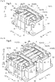
FIG. 5] FIG. 5 is a perspective view illustrating a switching element unit according to the embodiment. - [
FIG. 6] FIG. 6 is a perspective view illustrating a switching element module according to the embodiment. - [
FIG. 7] FIG. 7 is a configuration diagram illustrating an inverter circuit according to the embodiment. - [
FIG. 8] FIG. 8 is a perspective view illustrating a switching element module according to another embodiment. - An embodiment of a switching element unit and a switching element module will be described with reference to the drawings. It should be noted that, in the following description, the dimensions, the arrangement directions, the arrangement positions, and so on of members include differences caused by errors (allowable level of errors in manufacturing). Further, as used in this disclosure, the term "rotary electric machine" refers to any of a motor (electric motor), a generator (electric generator), and a motor generator that serve as both a motor and a generator as necessary.
- The
switching element unit 10 is used in an inverter circuit 100 (seeFIG. 7 ) that performs power conversion between DC power and AC power. AS illustrated inFIG. 7 , theinverter circuit 100 is disposed between a DC power supply 6 (DC voltage supply source) and a rotary electric machine MG. TheDC power supply 6 may include, for example, a battery or a capacitor. A capacitor 7 (smoothing capacitor) is disposed between theDC power supply 6 and theinverter circuit 100. Thecapacitor 7 smoothens the voltage on the DC side of theinverter circuit 100. The rotary electric machine MG is an AC rotary electric machine driven with AC power. The rotary electric machine MG is driven when AC power is supplied from theinverter circuit 100 to the rotary electric machine MG. The rotary electric machine MG is a rotary electric machine used in a vehicle such as an electric vehicle and a hybrid vehicle to serve as a driving force source of the vehicle (wheels). As will be described below in detail, theswitching element unit 10 may be used alone (seeFIG. 5 ), or may be used with one or moreswitching element units 10 connected in parallel (electrically connected in parallel) thereto (seeFIG. 6 ).FIG. 7 illustrates an example in which twoswitching element units 10, each forming oneinverter circuit 100, are connected in parallel. Thus, twoinverter circuits 100 are electrically connected in parallel to theDC power supply 6. In the present embodiment, the rotary electric machine MG corresponds to an "AC device". - As illustrated in
FIG. 7 , theinverter circuit 100 includes a bridge circuit. In the present embodiment, the bridge circuit includes arms equal in number to the number of phases. The arms are electrically connected in parallel. In the present embodiment, the rotary electric machine MG is an AC rotary electric machine driven with three-phase (an example of multi-phase) AC power, and the bridge circuit includes three arms electrically connected in parallel. Each arm includes a series circuit including an upper-stage switching element 30U of an upper-stage arm, and a lower-stage switching element 30L of a lower-stage arm. A positive-side end of the series circuit is connected to apositive bus bar 70P connected to apositive electrode 6P of theDC power supply 6, and a negative-side end of the series circuit is connected to anegative bus bar 70N connected to anegative electrode 6N of theDC power supply 6. Then, a midpoint (a connection point of the upper-stage switching element 30U and the lower-stage switching element 30L) of each of the plurality of arms is electrically connected to a coil (a stator coil in this example) of the corresponding phase of the rotary electric machine MG. It should be noted that a rectifying diode element 33 (freewheeling diode) is connected in parallel to each of the switching elements (30U, 30L). - A control terminal (a gate terminal in this example) of each of the switching elements (30U, 30L) is connected to a
control device 4 via adrive circuit 5. Then, the switching of each of the switching elements (30U, 30L) is controlled according to a switching control signal generated by thecontrol device 4, so that AC power is supplied from theinverter circuit 100 to the rotary electric machine MG. Unlike the example illustrated inFIG. 7 , the voltage between the positive electrode and the negative electrode of theDC power supply 6 may be increased or reduced and applied between thepositive bus bar 70P and thenegative bus bar 70N. In this case, thepositive bus bar 70P is connected to thepositive electrode 6P of theDC power supply 6 via a step-up circuit or a step-down circuit. - As illustrated in
FIGS. 1 to 4 , theswitching element unit 10 includes a switching element set 20, afirst bus bar 71, asecond bus bar 72, anoutput bus bar 40, and a moldedportion 2. As illustrated inFIG. 5 , in the present embodiment, theswitching element unit 10 is a unit that is integrated with thecapacitor 7 and acase 92 accommodating thecapacitor 7. However,FIGS. 1 and4 illustrate only a part thereof (mainly only a molded unit 3). The moldedunit 3 is a unit integrated by the moldedportion 2. Specifically, the moldedunit 3 includes the switching element set 20, thefirst bus bar 71, thesecond bus bar 72, and theoutput bus bar 40 that are integrated by the moldedportion 2. The moldedportion 2 is formed of a molding material (for example, resin), and is provided to hold the switching element set 20, thefirst bus bar 71, thesecond bus bar 72, and theoutput bus bar 40. - The switching element set 20 is a set of switching elements that form the inverter circuit 100 (see
FIG. 7 ). As illustrated inFIG. 4 , the switching element set 20 includes afirst switching element 31 connected to thefirst bus bar 71 and theoutput bus bar 40, and asecond switching element 32 connected to thesecond bus bar 72 and theoutput bus bar 40. In the present embodiment, the switching element set 20 includes onefirst switching element 31 and onesecond switching element 32. As illustrated inFIGS. 1 and4 , thefirst switching element 31 and thesecond switching element 32 are disposed to be embedded in the moldedportion 2. Theoutput bus bar 40 is connected to both thefirst switching element 31 and thesecond switching element 32. That is, theoutput bus bar 40 is disposed to electrically connect thefirst switching element 31 and thesecond switching element 32, and the potential of theoutput bus bar 40 corresponds to the potential of the midpoint of the arm of theinverter circuit 100. - Each of the
first switching element 31 and thesecond switching element 32 may be, for example, a power semiconductor element such as an IGBT (Insulated Gate Bipolar Transistor) and a MOSFET (Metal Oxide Semiconductor Field Effect Transistor). In the present embodiment, each of thefirst switching element 31 and thesecond switching element 32 is a chip-type element having adiode element 33 therein (seeFIG. 7 ). The chip-type element has a flat-plate-shaped outer contour, and is disposed such that the direction orthogonal to the plate surface is aligned with a below-described third direction Z. - The
first bus bar 71 is connected to one of thepositive electrode 6P and thenegative electrode 6N of theDC power supply 6, and thesecond bus bar 72 is connected to the other one of thepositive electrode 6P and thenegative electrode 6N of theDC power supply 6. In the present embodiment, the switchingelement unit 10 includes onefirst bus bar 71 and onesecond bus bar 72. As described above, thefirst switching element 31 is connected to thefirst bus bar 71 and theoutput bus bar 40, and thesecond switching element 32 is connected to thesecond bus bar 72 and theoutput bus bar 40. Accordingly, in the case where thefirst bus bar 71 is connected to thepositive electrode 6P of theDC power supply 6, and thesecond bus bar 72 is connected to thenegative electrode 6N of theDC power supply 6, that is, in the case where thefirst bus bar 71 serves as thepositive bus bar 70P, and thesecond bus bar 72 serves as thenegative bus bar 70N, thefirst switching element 31 serves as the upper-stage switching element 30U, and thesecond switching element 32 serves as the lower-stage switching element 30L. Further, in the case where thefirst bus bar 71 is connected to thenegative electrode 6N of theDC power supply 6, and thesecond bus bar 72 is connected to thepositive electrode 6P of theDC power supply 6, that is, in the case where thefirst bus bar 71 serves as thenegative bus bar 70N, and thesecond bus bar 72 serves as thepositive bus bar 70P, thefirst switching element 31 serves as the lower-stage switching element 30L, and thesecond switching element 32 serves as the upper-stage switching element 30U. In the present embodiment, thefirst bus bar 71 serves as thenegative bus bar 70N, and thesecond bus bar 72 serves as thepositive bus bar 70P. However, thefirst bus bar 71 may serve as thepositive bus bar 70P, and thesecond bus bar 72 may serve as thenegative bus bar 70N. - The
output bus bar 40 is connected to an AC device (the rotary electric machine MG in the present embodiment). In the present embodiment, theoutput bus bar 40 is electrically connected to the rotary electric machine MG via a device connection bus bar 91 (seeFIGS. 5 to 7 ). In the present embodiment, the switchingelement unit 10 includes a plurality of switching element sets 20, and a plurality of output bus bars 40 corresponding to the plurality of switching element sets 20. In this example, the switchingelement unit 10 includes the switching element sets 20 equal in number to the number of phases, and the output bus bars 40 equal in number to the number of phases. Specifically, as illustrated inFIG. 3 , the switchingelement unit 10 includes three switching element sets 20, namely, a first switching element set 21, a second switching element set 22, and a third switching element set 23, and includes three output bus bars 40, namely, a firstoutput bus bar 41, a secondoutput bus bar 42, and a thirdoutput bus bar 43. Accordingly, in the present embodiment, as illustrated inFIG. 7 , oneswitching element unit 10 forms oneinverter circuit 100. - As illustrated in
FIGS. 3 and 4 (see alsoFIG. 2 ), thefirst switching element 31 and thesecond switching element 32 included in each switching element set 20 are arranged side by side in a first direction X. Further, theoutput bus bar 40 is disposed to be in contact with thefirst switching element 31 and thesecond switching element 32 included in the corresponding switching element set 20. Specifically, theoutput bus bar 40 is disposed to extend in the first direction X while being in contact with the surface of thefirst switching element 31 opposite to the surface in contact with thefirst bus bar 71, and being in contact with the surface of thesecond switching element 32 opposite to the surface in contact with thesecond bus bar 72. The term "be in contact" as used herein means a state in which objects are in direct contact with each other or a state in which objects are in contact with each other with a bonding layer interposed therebetween. In the following description, one side in the first direction X (specifically, the side of the switching element set 20 on which a below-described first exposedportion 40a is disposed) is defined as a third side X1, and the side opposite to the third side X1 in the first direction X is defined as a fourth side X2. - Although not illustrated, each of the
first switching element 31 and thesecond switching element 32 includes a pair of main terminals (an emitter terminal and a collector terminal in the case where an IGBT is used as a switching element). The surface of thefirst switching element 31 in contact with thefirst bus bar 71 is formed such that one of the two main terminals is electrically connected to thefirst bus bar 71, and the surface of thefirst switching element 31 in contact with theoutput bus bar 40 is formed such that the other one of the two main terminals is electrically connected to theoutput bus bar 40. Further, the surface of thesecond switching element 32 in contact with thesecond bus bar 72 is formed such that one of the two main terminals is electrically connected to thesecond bus bar 72, and the surface of thesecond switching element 32 in contact with theoutput bus bar 40 is formed such that the other one of the two main terminals is electrically connected to theoutput bus bar 40. - As described above, in the present embodiment, the switching
element unit 10 includes the plurality of switching element sets 20. Accordingly, the switchingelement unit 10 includes the plurality offirst switching elements 31 and the plurality ofsecond switching elements 32. In the present embodiment, the switchingelement unit 10 includes thefirst switching elements 31 equal in number to the number of switching element sets 20, and thesecond switching elements 32 equal in number to the number of switching element sets 20. As illustrated inFIG. 3 , the plurality offirst switching elements 31 are arranged side by side in a second direction Y, and the plurality ofsecond switching elements 32 are arranged side by side in the second direction Y. Further, the plurality of output bus bars 40 are arranged side by side in the second direction Y in accordance with the arrangement of the plurality of switching element sets 20. Here, the second direction Y is the direction crossing the first direction X. In the present embodiment, the second direction Y is the direction orthogonal to the first direction X. In the following description, one side in the second direction Y is defined as a fifth side Y1, and the side opposite to the fifth side Y1 in the second direction Y is defined as a sixth side Y2. - As illustrated in
FIG. 4 , in the present embodiment, thefirst switching element 31 and thesecond switching element 32 included in each switching element set 20 are located in a common reference plane, namely, a first reference plane S1. In this example, all thefirst switching elements 31 and thesecond switching elements 32 included in theswitching element unit 10 are located in the first reference plane S1. Here, the orthogonal direction that is orthogonal to the first reference plane S1 is defined as a third direction Z. Further, one side in the third direction Z is defined as a first side Z1, and the side opposite to the first side Z1 in the third direction Z is defined as a second side Z2. The third direction Z coincides with the direction orthogonal to both the first direction X and the second direction Y - As illustrated in
FIG. 4 , theoutput bus bar 40 includes a first joiningportion 51b in contact with thefirst switching element 31, and a second joiningportion 52b in contact with thesecond switching element 32. Further, in the present embodiment, the first joiningportion 51b is disposed to be in contact with a surface on the first side Z1 of thefirst switching element 31, and the second joiningportion 52b is disposed to be in contact with a surface on the second side Z2 of thesecond switching element 32. Therefore, in the present embodiment, theoutput bus bar 40 includes abent portion 53 for locating the first joiningportion 51b on the first side Z1 with respect to the second joiningportion 52b, between the first joiningportion 51b and the second joiningportion 52b in the extending direction of theoutput bus bar 40. As illustrated inFIG. 4 , in the present embodiment, thebent portion 53 is formed such that a surface on the first side Z1 of the first joiningportion 51b and a surface on the first side Z1 of thesecond bus bar 72 are located in the same plane (in a below-described third reference plane S3) parallel to the first reference plane S1, and such that a surface on the second side Z2 of the second joiningportion 52b and a surface on the second side Z2 of thefirst bus bar 71 are located in the same plane (in a below-described second reference plane S2) parallel to the first reference plane S1. - As illustrated in
FIGS. 1 to 3 , each of thefirst bus bar 71 and thesecond bus bar 72 is disposed to extend in the second direction Y. Specifically thefirst bus bar 71 is disposed to extend in the second direction Y while being in contact with all the first switching elements 31 (threefirst switching elements 31 in this example). In the present embodiment, since the first joiningportion 51b of theoutput bus bar 40 is in contact with the surface on the first side Z1 of thefirst switching element 31, thefirst bus bar 71 is disposed to be in contact with a surface on the second side Z2 of thefirst switching element 31. Further, thesecond bus bar 72 is disposed to extend in the second direction Y while being in contact with all the second switching elements 32 (threesecond switching elements 32 in this example). In the present embodiment, since the second joiningportion 52b of theoutput bus bar 40 is in contact with the surface on the second Z2 side of thesecond switching element 32, thesecond bus bar 72 is disposed to be in contact with a surface on the first side Z1 of thesecond switching element 32. - The switching
element unit 10 is designed not only to be used alone, but also to be used with one or moreswitching element units 10 connected in parallel (electrically connected in parallel) thereto. The number and combination of switchingelement units 10 to be connected in parallel may be changed so as to adjust the current capacity as a whole. For example, assume that aswitching element unit 10 with a current capacity of C1 [A] (hereinafter referred to as a "first-type unit") and aswitching element unit 10 with a current capacity of C2 [A] (hereinafter referred to as a "second-type unit") are manufactured, and a single unit is used, or two units are connected in parallel and used. Then, the current capacity is adjustable to any of the following five: C1 [A] in the case where a single first-type unit is used; C2 [A] in the case where a single second-type unit is used; (2×C1) [A] in the case two first-type units connected in parallel are used; (C1+C2) [A] in the case where a single first-type unit and a single second-type unit connected in parallel are used; and (2×C2) [A] in the case where two second-type units connected in parallel are used. - In the case where the switching
element unit 10 is not only used alone, but also used with one or moreswitching element units 10 connected in parallel thereto, it is preferable that the electrical connection structure for electrically connecting the plurality of switchingelement units 10 in parallel is simple. In the following, a description will be given of the configuration that simplifies the electrical connection structure for connecting the plurality of switchingelement units 10 in parallel, in theswitching element unit 10 according to the present embodiment. - As illustrated in
FIGS. 1 and4 , theoutput bus bar 40 includes an embeddedportion 40c embedded in the moldedportion 2, a first exposedportion 40a exposed from the moldedportion 2 on one side (the third side X1) of the corresponding switching element set 20 in the first direction X, and a second exposedportion 40b exposed from the moldedportion 2 on the other side (the fourth side X2) of the corresponding switching element set 20 in the first direction X. In the present embodiment, both the first exposedportion 40a and the second exposedportion 40b are defined by regions of theoutput bus bar 40 exposed from the moldedportion 2 to the second side Z2. - Specifically, as illustrated in
FIG. 4 , theoutput bus bar 40 includes, sequentially from one side in the extending direction of theoutput bus bar 40, a first extendingportion 51a, the above-described first joiningportion 51b, the above-described second joiningportion 52b, and a second extendingportion 52a. Then, the first extendingportion 51a includes afirst part 61 extending in the first direction X from the first joiningportion 51b to the third side X1, and asecond part 62 extending from an end of thefirst part 61 on the side opposite to the first joiningportion 51b (that is, an end on the third side X1) to the second side Z2. It should be noted that thesecond part 62 extends to the second side Z2 so as to be exposed from the moldedportion 2 to the second side Z2. The second extendingportion 52a includes athird part 63 extending in the first direction X from the second joiningportion 52b to the fourth side X2. A surface on the second side Z2 of the second joiningportion 52b is exposed from the moldedportion 2 to the second side Z2, and thethird part 63 extends in the first direction X from the second joiningportion 52b while being exposed from the moldedportion 2 to the second side Z2. The region of thesecond part 62 exposed from the moldedportion 2 to the second side Z2 defines the first exposedportion 40a, and the region of thethird part 63 exposed from the moldedportion 2 to the second side Z2 defines the second exposedportion 40b. - As illustrated in
FIG. 1 , in the present embodiment, thefirst bus bar 71 is disposed to be exposed from the moldedportion 2, on both sides of the plurality of first switching elements 31 (three first switching elements in this example; the same applies to the following description) in the second direction Y. Specifically, thefirst bus bar 71 includes a thirdexposed portion 71a exposed from the moldedportion 2 on the fifth side Y1 of the plurality offirst switching elements 31, and a fourth exposedportion 71b exposed from the moldedportion 2 on the sixth side Y2 of the plurality offirst switching elements 31. In the present embodiment, as illustrated inFIG. 1 , thefirst bus bar 71 is disposed to be exposed from the moldedportion 2 to the second side Z2, throughout the region in the second direction Y where the plurality offirst switching elements 31 are disposed. The region of thefirst bus bar 71 exposed from the moldedportion 2 to the second side Z2 on the fifth side Y1 of the plurality offirst switching elements 31 defines the thirdexposed portion 71a, and the region of thefirst bus bar 71 exposed from the moldedportion 2 to the second side Z2 on the sixth side Y2 of the plurality offirst switching elements 31 defines the fourth exposedportion 71b. - Further, as illustrated in
FIG. 1 , in the present embodiment, thesecond bus bar 72 is disposed to be exposed from the moldedportion 2, on both sides of the plurality of second switching elements 32 (threesecond switching elements 32 in this example; the same applies to the following description) in the second direction Y. Specifically, thesecond bus bar 72 includes a fifth exposedportion 72a exposed from the moldedportion 2 on the fifth side Y1 of the plurality ofsecond switching elements 32, and a sixth exposedportion 72b exposed from the moldedportion 2 on the sixth side Y2 of the plurality ofsecond switching elements 32. In the present embodiment, as illustrated inFIG. 2 , thesecond bus bar 72 is formed such that an end thereof on the fifth side Y1 extends to the second side Z2 so as to be exposed from the moldedportion 2 to the second side Z2, on the fifth side Y1 of the plurality ofsecond switching elements 32, and the region exposed from the moldedportion 2 to the second side Z2 at the end of thesecond bus bar 72 on the fifth side Y1 defines the fifth exposedportion 72a. Further, thesecond bus bar 72 is formed such that an end thereof on the sixth side Y2 extends to the second side Z2 so as to be exposed from the moldedportion 2 to the second side Z2, on the sixth side Y2 of the plurality ofsecond switching elements 32, and the region exposed from the moldedportion 2 to the second side Z2 at the end of thesecond bus bar 72 on the sixth side Y2 defines the sixth exposedportion 72b. - As described above, the
output bus bar 40 includes the exposed portions (40a, 40b) exposed from the moldedportion 2, on both sides of the switching element set 20 in the first direction X. Further, in the present embodiment, thefirst bus bar 71 includes the exposed portions (71a, 71b) exposed from the moldedportion 2, on both sides of the plurality offirst switching elements 31 in the second direction Y, and thesecond bus bar 72 includes the exposed portions (72a, 72b) exposed from the moldedportion 2, on both sides of the plurality ofsecond switching elements 32 in the second direction Y. Since the switchingelement unit 10 is configured as described above, it is possible to simplify the electrical connection structure for connecting the plurality of switchingelement units 10 in parallel as will be descried below. - As illustrated in
FIG. 6 , aswitching element module 1 is a module including a plurality of switchingelement units 10. InFIGS. 5 and 6 andFIG. 8 to be referred to later, the moldedportion 2 is not illustrated for easy understanding of the arrangement configuration of theoutput bus bar 40 and other elements. The plurality of switchingelement units 10 of theswitching element module 1 include a firstswitching element unit 11 and a secondswitching element unit 12 arranged side by side in the first direction X. The firstswitching element unit 11 is disposed on the third side X1 of the secondswitching element unit 12 in the first direction X. As illustrated inFIG. 6 , the firstswitching element unit 11 and the secondswitching element unit 12 basically have the same configuration except that only the secondswitching element unit 12 is provided with acurrent sensor 8 that detects current flowing through the deviceconnection bus bar 91. The firstswitching element unit 11 and the secondswitching element unit 12 are arranged side by side in the first direction X, in the same position in the second direction Y. Accordingly, a firstoutput bus bar 41 of the firstswitching element unit 11 and a firstoutput bus bar 41 of the secondswitching element unit 12 are arranged side by side in the first direction X; a secondoutput bus bar 42 of the firstswitching element unit 11 and a secondoutput bus bar 42 of the secondswitching element unit 12 are arranged side by side in the first direction X; and a thirdoutput bus bar 43 of the firstswitching element unit 11 and a thirdoutput bus bar 43 of the secondswitching element unit 12 are arranged side by side in the first direction X. - Further, as illustrated in
FIG. 6 (see alsoFIG. 2 ), a second exposedportion 40b of the first switching element unit 11 (a second exposedportion 40b of theoutput bus bar 40 of the first switching element unit 11) and a first exposedportion 40a of the second switching element unit 12 (a first exposedportion 40a of theoutput bus bar 40 of the second switching element unit 12) are connected to each other with aconnection bus bar 90 disposed to extend in the first direction X. Specifically, a second exposedportion 40b of the firstoutput bus bar 41 of the firstswitching element unit 11 and a first exposedportion 40a of the firstoutput bus bar 41 of the secondswitching element unit 12 are connected to each other with a connection bus bar 90 (first connection bus bar). Also, a second exposedportion 40b of the secondoutput bus bar 42 of the firstswitching element unit 11 and a first exposedportion 40a of the secondoutput bus bar 42 of the secondswitching element unit 12 are connected to each other with a connection bus bar 90 (second connection bus bar). Further, a second exposedportion 40b of the thirdoutput bus bar 43 of the firstswitching element unit 11 and a first exposedportion 40a of the thirdoutput bus bar 43 of the secondswitching element unit 12 are connected to each other with a connection bus bar 90 (third connection bus bar). - In this manner, the plurality of switching
element units 10 are arranged in the first direction X, and the second exposedportion 40b of the switchingelement unit 10 of the two adjacentswitching element units 10 that is disposed on the third side X1 (the firstswitching element unit 11 in the example ofFIG. 6 ) and the first exposedportion 40a of the switchingelement unit 10 that is disposed on the fourth side X2 (the secondswitching element unit 12 in the example ofFIG. 6 ) are connected to each other. Thus, the output bus bars 40 can be connected to each other without interposing any of the switching element sets 20 of these two switchingelement units 10. Moreover, since two output bus bars 40 to be connected are arranged side by side in the first direction X, the output bus bars 40 can be connected to each other without interposing an electrical connection structure for connecting other output bus bars 40 to each other. This makes it possible to simplify the electrical connection structure for connecting the output bus bars 40 to each other. - In the example illustrated in
FIG. 6 , the deviceconnection bus bar 91 is connected to a second exposedportion 40b of theoutput bus bar 40 of the secondswitching element unit 12. Specifically, device connection bus bars 91 are connected to the respective second exposedportions 40b of the plurality of output bus bars 40 (three output bus bars 40 in this example) of the secondswitching element unit 12. As described above, since two switching element units 10 (the firstswitching element unit 11 and the second switching element unit 12) are connected in parallel, a circuit having twoinverter circuits 100 electrically connected in parallel is formed as illustrated inFIG. 7 . - As illustrated in
FIG. 6 , in the present embodiment, each of the firstswitching element unit 11 and the secondswitching element unit 12 is a unit that is integrated with thecapacitor 7 electrically connected in parallel to the series circuit of thefirst switching element 31 and thesecond switching element 32 included in the switching element set 20. That is, in the present embodiment, the switchingelement unit 10 is a unit integrated with thecapacitor 7. - Specifically, as illustrated in
FIG. 5 , the switchingelement unit 10 includes thecapacitor 7, and thecase 92 accommodating thecapacitor 7, in addition to the moldedunit 3. Although not described in detail, in the present embodiment, thecase 92 accommodates a plurality of capacitor elements included in thecapacitor 7. The moldedunit 3 is fixed to a fixingportion 93 formed on thecase 92. As illustrated inFIG. 4 , the upper surface of the fixingportion 93 is a flat surface, and the moldedunit 3 is fixed to the fixingportion 93 from the second side Z2. Although not illustrated, in the present embodiment, an insulating resin sheet (adhesive sheet) is interposed between the moldedunit 3 and the fixingportion 93. Further, in the present embodiment, the fixingportion 93 is cooled by a cooling device provided in thecase 92. That is, the fixingportion 93 is configured to serve as a heatsink, and is capable of cooling the members included in the moldedunit 3 fixed to the fixingportion 93, by using the cooling device. That is, a surface on the first side of the moldedunit 3 Z1 is a cooledsurface 3a that is cooled by the cooling device. - As illustrated in
FIG. 5 , thecapacitor 7 includes afirst terminal 7a connected to thefirst bus bar 71, and asecond terminal 7b connected to thesecond bus bar 72. In the case where thefirst bus bar 71 serves as thepositive bus bar 70P, and thesecond bus bar 72 serves as thenegative bus bar 70N, thefirst terminal 7a serves as a positive terminal 7P of thecapacitor 7, and thesecond terminal 7b serves as anegative terminal 7N of thecapacitor 7. Whereas, in the case where thefirst bus bar 71 serves as thenegative bus bar 70N, and thesecond bus bar 72 serves as thepositive bus bar 70P, thefirst terminal 7a serves as thenegative terminal 7N of thecapacitor 7, and thesecond terminal 7b serves as the positive terminal 7P of thecapacitor 7. In the present embodiment, thecapacitor 7 includes a set of thefirst terminal 7a and thesecond terminal 7b, on each side of the moldedunit 3 in the second direction Y. Then, as illustrated inFIG. 5 (see alsoFIG. 2 ), the thirdexposed portion 71a of thefirst bus bar 71 and thefirst terminal 7a on the fifth side Y1 are connected (with a firstelectrode bus bar 81 in this example), and the fourth exposedportion 71b of thefirst bus bar 71 and thefirst terminal 7a on the sixth side Y2 are connected (with another firstelectrode bus bar 81 in this example). Also, the fifth exposedportion 72a of thesecond bus bar 72 and thesecond terminal 7b on the fifth side Y1 are connected (with a secondelectrode bus bar 82 in this example), and the sixth exposedportion 72b of thesecond bus bar 72 and thesecond terminal 7b on the sixth side Y2 are connected (with another secondelectrode bus bar 82 in this example). In this manner, in the present embodiment, thefirst bus bar 71 and thesecond bus bar 72 are connected to thecapacitor 7 on both sides of the switching element set 20 in the second direction Y Therefore, the effective wiring length between the switching element set 20 and thecapacitor 7 is reduced, thereby reducing the inductance. - Although not illustrated, the plurality of switching
element units 10 of theswitching element module 1 may include two switchingelement units 10 arranged side by side in the second direction Y In this case, a fourth exposedportion 71b of afirst bus bar 71 of the switchingelement unit 10 disposed on the fifth side Y1 among the two switchingelement units 10 adjacent in the second direction Y and a thirdexposed portion 71a of afirst bus bar 71 of the switchingelement unit 10 disposed on the sixth side Y2 are connected to each other. This makes it possible to simplify the electrical connection structure for connecting the first bus bars 71. Similarly, a sixth exposedportion 72b of asecond bus bar 72 of the switchingelement unit 10 disposed on the fifth side Y1 among the two switchingelement units 10 adjacent in the second direction Y and a fifth exposedportion 72a of asecond bus bar 72 of the switchingelement unit 10 disposed on the sixth side Y2 are connected to each other. This makes it possible to simplify the electrical connection structure for connecting the second bus bars 72. - As illustrated in
FIG. 4 , in the present embodiment, a firstdistal end 62a defining a distal end (an end face on the second side Z2) of thesecond part 62, a surface on the second side Z2 of the second joiningportion 52b, and a surface on the second side Z2 of thethird part 63 are located in the same plane (in the second reference plane S2 in this example) parallel to the first reference plane S1. The second reference plane S2 is located on the second side Z2 with respect to an end face on the second side Z2 of the moldedportion 2. In the present embodiment, the surface on the second side Z2 of thefirst bus bar 71 and surfaces on the second side Z2 at both ends of thesecond bus bar 72 in the second direction Y (distal ends (end faces on the second side Z2) of the portions defining the exposed portions (72a, 72b)) are also located in the second reference plane S2. Accordingly, when the moldedunit 3 is press-fitted and fixed to the fixingportion 93 from the second side Z2 during manufacture of the switchingelement unit 10, the plurality of portions located in the second reference plane S2 serve as pressed portions that are pressed to the first side Z1 by a jig or the like. Since the plurality of pressed portions are located in the same plane, it is easy to apply a load uniformly to the plurality of pressed portions and appropriately press-fit the moldedunit 3 to the fixingportion 93. - Also, as illustrated in
FIG. 4 , in the present embodiment, the second extendingportion 52a of theoutput bus bar 40 includes afourth part 64 extending from an end of thethird part 63 on the side opposite to the second joiningportion 52b (that is, an end on the fourth side X2) to the first side Z1. Further, a seconddistal end 64a defining a distal end (an end face on the first side Z1) of thefourth part 64, the surface on the first side Z1 of the first joiningportion 51b, and a surface on the first side Z1 of thefirst part 61 are located in the same plane (in the third reference plane S3 in this example) parallel to the first reference plane S1. InFIG. 4 , the third reference plane S3 is located in the same position as an end face on the first side Z1 of the moldedportion 2. However, the third reference plane S3 may be a plane displaced from the end face on the first side Z1 of the moldedportion 2 to the first side Z1 or to the second side Z2. In the present embodiment, the surface on the first side Z1 of thesecond bus bar 72, a thirddistal end 71c of thefirst bus bar 71, and a fourthdistal end 71d of thefirst bus bar 71 are also located in the third reference plane S3. As illustrated inFIG. 2 , in the present embodiment, thefirst bus bar 71 is formed such that an end thereof on the fifth side Y1 extends to the first side Z1, on the fifth side Y1 of the plurality offirst switching elements 31, and an end face on the first side Z1 at the end of thefirst bus bar 71 on the fifth side Y1 defines the thirddistal end 71c. Also, thefirst bus bar 71 is formed such that an end thereof on the sixth side Y2 extends to the first side Z1, on the sixth side Y2 of the plurality offirst switching elements 31, and an end face on the first side Z1 at the end on the sixth side Y2 of thefirst bus bar 71 defines the fourthdistal end 71d. - As described above, in the present embodiment, since the second
distal end 64a, the surface on the first side Z1 of the first joiningportion 51b, and the surface on the first side Z1 of thefirst part 61 are disposed in the third reference plane S3, these elements are disposed close to the cooling device (fixing portion 93) (for example, disposed to face the fixing portion 93) that cools the cooledsurface 3a. This makes it possible to efficiently cool theoutput bus bar 40. Further, in the present embodiment, since the surface on the first side Z1 of thesecond bus bar 72, the thirddistal end 71c of thefirst bus bar 71, and the fourthdistal end 71d of thefirst bus bar 71 are also located in the third reference plane S3, these elements are disposed close to the cooling device (fixing portion 93) (for example, disposed to face the fixing portion 93) that cools the cooledsurface 3a. This makes it possible to efficiently cool thefirst bus bar 71 and thesecond bus bar 72. - Moreover, when the molded
unit 3 is press-fitted and fixed to the fixingportion 93 from the second side Z2 during manufacture of the switchingelement unit 10, a plurality of portions located in the third reference plane S3 serve as support portions that receive a pressing load applied to the moldedunit 3. That is, theoutput bus bar 40, thefirst bus bar 71, and thesecond bus bar 72 are configured such that their end faces on the second side Z2 serve as the pressed portions described above, and their end faces on the first side Z1 serve as the support portions described herein. This makes it possible to appropriately protect the switching element set 20 while reducing the pressing load applied to the switching element set 20 in the press-fitting and fixing step. - The following describes other embodiments of a switching element unit and a switching element module.
- (1) In the above embodiment, each switching
element unit 10 includes first switchingelements 31 equal in number to the number of phases, andsecond switching elements 32 equal in number to the number of phases. However, the present invention is not limited to this configuration. Each switchingelement unit 10 may includefirst switching elements 31 different in number from the number of phases, andsecond switching elements 32 different in number from the number of phases.FIG. 8 illustrates an example of this configuration.
In the example illustrated inFIG. 8 , a switchingelement unit 10 corresponds to two switchingelement units 10 ofFIG. 6 integrated by combining thecases 92 of the two switchingelement units 10 into asingle case 92. Therefore, the switchingelement unit 10 ofFIG. 8 includes two moldedunits 3 ofFIG. 1 , and includes twice the number offirst switching elements 31 as the number of phases, and twice the number ofsecond switching elements 32 as the number of phases. In this case, a singleswitching element unit 10 forms two inverter circuits 100 (seeFIG. 7 ) that are electrically connected in parallel to each other. Further, in this case, unlike the above embodiment, the singleswitching element unit 10 includes twice the number of switching element sets 20 as the number of phases, and twice the number of output bus bars 40 as the number of phases.
In the configuration illustrated inFIG. 8 , two output bus bars 40 arranged side by side in the first direction X may be formed integrally, and theconnection bus bar 90 may not be provided. In this case, unlike the above embodiment, a first exposedportion 40a of eachoutput bus bar 40 is formed to be exposed from the moldedportion 2, on the third side X1 of the switching element set 20 including twofirst switching elements 31 and twosecond switching elements 32. Further, a second exposedportion 40b of eachoutput bus bar 40 is formed to be exposed from the moldedportion 2, on the fourth side X2 of the switching element set 20 including twofirst switching elements 31 and twosecond switching elements 32. In this manner, a single switching element set 20 may include a plurality offirst switching elements 31 and a plurality ofsecond switching elements 32. - (2) In the above embodiment, the rotary electric machine MG is an AC rotary electric machine driven with multi-phase AC power. However, the rotary electric machine MG may be an AC rotary electric machine driven with single-phase AC power. In this case, the switching
element unit 10 may include two switching element sets 20, instead of including switching element sets 20 equal in number to the number of phases (specifically, three switching element sets 20) as in the above embodiments. - (3) In the above embodiment, each switching
element unit 10 includes the required number of (three in the above embodiment) switching element sets 20 to form asingle inverter circuit 100. However, the present invention is not limited to this configuration. Each switchingelement unit 10 may include less than the required number of switching element sets 20 (for example, one switching element set 20) to form asingle inverter circuit 100, and a plurality of switching element units 10 (for example, a plurality of switchingelement units 10 arranged side by side in the second direction Y) may form asingle inverter circuit 100. - (4) In the above embodiment, the second exposed
portion 40b of the firstswitching element unit 11 and the first exposedportion 40a of the secondswitching element unit 12 are connected to each other with theconnection bus bar 90 disposed to extend in the first direction X. However, the present invention is not limited to this configuration. Theoutput bus bar 40 may be formed in a shape such that the second exposedportion 40b of the firstswitching element unit 11 and the first exposedportion 40a of the secondswitching element unit 12 are in contact with each other, so that the second exposedportion 40b of the firstswitching element unit 11 and the first exposedportion 40a of the secondswitching element unit 12 may be directly connected to each other. - (5) In the above embodiment, the first
distal end 62a defining the distal end of thesecond part 62, the surface on the second side Z2 of the second joiningportion 52b, and the surface on the second side Z2 of thethird part 63 are located in the same plane (in the second reference plane S2) parallel to the first reference plane S1. However, the present invention is not limited to this configuration. For example, the firstdistal end 62a may be located in a position different from the positions of the surface on the second side Z2 of the second joiningportion 52b and the surface on the second side Z2 of thethird part 63, in the third direction Z. - (6) In the above embodiment, the second extending
portion 52a of theoutput bus bar 40 includes thefourth part 64. However, the present invention is not limited thereto. The second extendingportion 52a may not include thefourth part 64. - (7) In the above embodiment, both the first exposed
portion 40a and the second exposedportion 40b are defined by regions of theoutput bus bar 40 exposed from the moldedportion 2 to the second side Z2. However, the present invention is not limited to this configuration. The first exposedportion 40a may be defined by a region of theoutput bus bar 40 exposed from the moldedportion 2 to the third side X1, or the first exposedportion 40a may be defined by both a region of theoutput bus bar 40 exposed from the moldedportion 2 to the second side Z2 and a region exposed to the third side X1. Also, the second exposedportion 40b may be defined by a region of theoutput bus bar 40 exposed from the moldedportion 2 to the fourth side X2, or the second exposedportion 40b may be defined by both a region of theoutput bus bar 40 exposed from the moldedportion 2 to the second side Z2 and a region exposed to the fourth side X2. - (8) In the above embodiment, both the third
exposed portion 71a and the fourth exposedportion 71b are defined by regions of thefirst bus bar 71 exposed from the moldedportion 2 to the second side Z2. However, the present invention is not limited to this configuration. The thirdexposed portion 71a may be defined by a region of thefirst bus bar 71 exposed from the moldedportion 2 to the fifth side Y1, or the thirdexposed portion 71a may be defined by both a region of thefirst bus bar 71 exposed from the moldedportion 2 to the second side Z2 and a region exposed to the fifth side Y1. Also, the fourth exposedportion 71b may be defined by a region of thefirst bus bar 71 exposed from the moldedportion 2 to the sixth side Y2, or the fourth exposedportion 71b may be defined by both a region of thefirst bus bar 71 exposed from the moldedportion 2 to the second side Z2 and a region exposed to the sixth side Y2. - (9) In the above embodiment, both the fifth exposed
portion 72a and the sixth exposedportion 72b are defined by regions of thesecond bus bar 72 exposed from the moldedportion 2 to the second side Z2. However, the present invention is not limited to this configuration. The fifth exposedportion 72a may be defined by a region of thesecond bus bar 72 exposed from the moldedportion 2 to the fifth side Y1, or the fifth exposedportion 72a may be defined by both a region of thesecond bus bar 72 exposed from the moldedportion 2 to the second side Z2 and a region exposed to the fifth side Y1. Also, the sixth exposedportion 72b may be defined by a region of thesecond bus bar 72 exposed from the moldedportion 2 to the sixth side Y2, or the sixth exposedportion 72b may be defined by both a region of thesecond bus bar 72 exposed from the moldedportion 2 to the second side Z2 and a region exposed to the sixth side Y2. - (10) In the above embodiment, the
first bus bar 71 is disposed to be exposed from the moldedportion 2, on both sides of the plurality offirst switching elements 31 in the second direction Y, and thesecond bus bar 72 is disposed to be exposed from the moldedportion 2, on both sides of the plurality ofsecond switching elements 32 in the second direction Y However, the present invention is not limited to this configuration. Thefirst bus bar 71 may be disposed to be exposed from the moldedportion 2, only on one side of the plurality offirst switching elements 31 in the second direction Y Also, thesecond bus bar 72 may be disposed to be exposed from the moldedportion 2, only on one side of the plurality ofsecond switching elements 32 in the second direction Y - (11) In the present embodiment, the
first switching element 31 and thesecond switching element 32 are located in a common reference plane (in the first reference plane S1). However, the present invention is not limited to this configuration. Thefirst switching element 31 and thesecond switching element 32 may be located in different positions from each other in the third direction Z (the direction orthogonal to both the first direction X and the second direction Y). In such a case, unlike the above embodiment, theoutput bus bar 40 may not include thebent portion 53, and the first joiningportion 51b and the second joiningportion 52b may be located in the same plane. - (12) In the above embodiment, the first joining
portion 51b is disposed to be in contact with the surface on the first side Z1 of thefirst switching element 31, and the second joiningportion 52b is disposed to be in contact with the surface on the second side Z2 of thesecond switching element 32. However, the present invention is not limited to this configuration. The first joiningportion 51b may be disposed to be in contact with the surface on the second side Z2 of thefirst switching element 31, and the second joiningportion 52b may be disposed to be in contact with the surface on the first side Z1 of thesecond switching element 32. Alternatively, the first joiningportion 51b may be disposed to be in contact with the surface of thefirst switching element 31 on the second side Z2, and the second joiningportion 52b may be disposed to be in contact with the surface on the second side Z2 of thesecond switching element 32. Further alternatively, the first joiningportion 51b may be disposed to be in contact with the surface on the first side Z1 of thefirst switching element 31, and the second joiningportion 52b may be disposed to be in contact with the surface on the first side Z1 of thesecond switching element 32. In such a case, unlike the above embodiment, theoutput bus bar 40 may not include thebent portion 53, and the first joiningportion 51b and the second joiningportion 52b may be located in the same plane. - (13) In the above embodiment, the switching
element unit 10 is a unit integrated with thecapacitor 7 by thecase 92. However, the present invention is not limited to this configuration. The switchingelement unit 10 and thecapacitor 7 may not be integrated. For example, the switchingelement unit 10 and thecapacitor 7 may be accommodated in different cases. - (14) The features disclosed in any of the embodiments described above (including the embodiments described as other embodiments) may be applied in combination with the features disclosed in the other embodiments as long as no inconsistency arises. Regarding other features as well, the embodiments disclosed herein are merely examples in all respects. Accordingly, various modifications may be appropriately made without departing from the scope and spirit of the present disclosure.
- The following provides a summary of the switching element unit and the switching element module described above.
- A switching element unit (10) includes: a switching element set (20) that forms an inverter circuit (100); a first bus bar (71) connected to one of a positive electrode (6P) and a negative electrode (6N) of a DC power supply (6); a second bus bar (72) connected to another of the positive electrode (6P) and the negative electrode (6N) of the DC power supply (6); an output bus bar (40) connected to an AC device (MG); and a molded portion (2); wherein the switching element set (20) includes a first switching element (31) connected to the first bus bar (71) and the output bus bar (40), and a second switching element (32) connected to the second bus bar (72) and the output bus bar (40); wherein the first switching element (31) and the second switching element (32) are arranged side by side in a first direction (X); wherein the output bus bar (40) is disposed to extend in the first direction (X) while being in contact with a surface of the first switching element (31) opposite to a surface in contact with the first bus bar (71), and being in contact with a surface of the second switching element (32) opposite to a surface in contact with the second bus bar (72); wherein the first switching element (31) and the second switching element (32) are disposed to be embedded in the molded portion (2); and wherein the output bus bar (40) includes an embedded portion (40c) embedded in the molded portion (2), a first exposed portion (40a) exposed from the molded portion (2) on one side of the switching element set (20) in the first direction (X), and a second exposed portion (40b) exposed from the molded portion (2) on another side of the switching element set (20) in the first direction (X).
- When connecting a plurality of switching element units (10) having this configuration in parallel, switching elements included in different switching element units (10) can be electrically connected in parallel to each other by connecting output bus bars (40) included in the different switching element units (10) to each other, first bus bars (71) to each other, and second bus bars (72) to each other. According to the above configuration, the output bus bar (40) includes the exposed portions (40a, 40b) exposed from the molded portion (2), on both sides of the switching element set (20) in the first direction (X). Accordingly, a plurality of switching element units (10) to be connected are arranged side by side in the same orientation in the first direction (X), thereby making it possible to simplify the electrical connection structure for connecting the output bus bars (40) to each other. Specifically, the first exposed portion (40a) of the output bus bar (40) of one switching element unit (10) of two switching element units (10) adjacent in the first direction (X) and the second exposed portion (40b) of the output bus bar (40) of the other switching element unit (10) are connected, so that the output bus bars (40) can be connected to each other without interposing any of the switching element sets (20) of the two switching element units (10). This makes it possible to simplify the electrical connection structure for connecting the output bus bars (40) to each other.
- When arranging the plurality of switching element units (10) side by side in the first direction (X) and connecting the output bus bars (40) of two adjacent switching element units (10) to each other in the manner described above, the output bus bar (40) of either one of the switching element units (10) is connected to the AC device (MG). Thus, all the output bus bars (40) of the plurality of switching element units (10) can be electrically connected to the AC device (MG). In this case, of the exposed portions (40a, 40b) of the output bus bar (40) of the switching element unit (10) disposed at the end in the first direction (X), the exposed portion not connected to the output bus bar (40) of another switching element unit (10) adjacent in the first direction (X) is connected to the AC device (MG). Thus, it is possible to provide an electrical connection structure between the switching element unit (10) and the AC device (MG), while avoiding interference with the electrical connection structure for connecting the output bus bars (40) to each other.
- As described above, according to the above configuration, when connecting a plurality of switching element units (10) in parallel, it is possible to simplify the electrical connection structure for electrically connecting switching elements included in different switching element units (10) in parallel to each other.
- The first switching element (31) and the second switching element (32) may be located in a common reference plane (S1); one side in an orthogonal direction (Z) orthogonal to the reference plane (S1) may be defined as a first side (Z1), and a side opposite to the first side (Z1) in the orthogonal direction (Z) may be defined as a second side (Z2); the output bus bar (40) may include, sequentially from one side in an extending direction of the output bus bar (40), a first extending portion (51a), a first joining portion (51b) in contact with a surface on the first side (Z1) of the first switching element (31), a second joining portion (52b) in contact with a surface on the second side (Z2) of the second switching element (32), and a second extending portion (52a); the first extending portion (51a) may include a first part (61) extending in the first direction (X) from the first joining portion (51b), and a second part (62) extending from an end of the first part (61) on a side opposite to the first joining portion (51b) to the second side (Z2); the second extending portion (52a) may include a third part (63) extending in the first direction (X) from the second joining portion (52b); a region of the second part (62) exposed from the molded portion (2) to the second side (Z2) may define the first exposed portion (40a); and a region of the third part (63) exposed from the molded portion (2) to the second side (Z2) may define the second exposed portion (40b).
- According to this configuration, the output bus bar (40) includes the first joining portion (51b) in contact with the surface on the first side (Z1) of the first switching element (31), and the second joining portion (52b) in contact with the surface on the second side (Z2) of the second switching element (32) opposite to the first side (Z1). Accordingly, even in the case where the first switching element (31) and the second switching element (32) are located in the common reference plane (S1), the first switching element (31) and the second switching element (32) can be disposed such that the same surfaces face the same side in the orthogonal direction (Z) (for example, the surfaces provided with a control terminal, such as a gate terminal, face the second side (Z2)). Further, according to the above configuration, even in the case where the output bus bar (40) is formed in a shape that allows this arrangement of the first switching element (31) and the second switching element (32), the output bus bar (40) can be formed to have both the first exposed portion (40a) and the second exposed portion (40b).
- In the above configuration in which the region of the second part (62) exposed from the molded portion (2) to the second side (Z2) defines the first exposed portion (40a), and the region of the third part (63) exposed from the molded portion (2) to the second side (Z2) defines the second exposed portion (40b), a distal end (62a) of the second part (62), a surface on the second side (Z2) of the second joining portion (52b), and a surface on the second side (Z2) of the third part (63) may be located in a same plane parallel to the reference plane (S1).
- According to this configuration, when a molded unit (3) formed by integrating the switching element set (20) and the output bus bar (40) with the molded portion (2) is press-fitted and fixed to a fixing portion (93) from the second side (Z2), the distal end (62a) of the second part (62), the surface on the second side (Z2) of the second joining portion (52b), and the surface on the second side (Z2) of the third part (63) serve as pressed portions that are pressed to the first side (Z1) by a jig or the like. Further, according to the above configuration, since these three pressed portions are located in the same plane, it is easy to apply a load uniformly to these three pressed portions and appropriately press-fit the molded unit (3) to the fixing portion (93).
- Further, the second extending portion (52a) may include a fourth part (64) extending from an end of the third part (63) on a side opposite to the second joining portion (52b) to the first side (Z1), and a distal end (64a) of the fourth part (64), a surface on the first side (Z1) of the first joining portion (51b), and a surface on the first side (Z1) of the first part (61) may be located in a same plane parallel to the reference plane (S1).
- According to this configuration, in the case where a surface on the first side (Z1) of the molded unit (3) formed by integrating the switching element set (20) and the output bus bar (40) with the molded portion (2) is a cooled surface (3a) that is cooled by the cooling device, not only the surface on the first side (Z1) of the first joining portion (51b) and the surface on the first side (Z1) of the first part (61), but also the distal end (64a) of the fourth part (64) can be disposed close to the cooling device (for example, disposed to face the cooling device). This makes it possible to efficiently cool the output bus bar (40). Further, according to the above configuration, when the molded unit (3) is press-fitted and fixed to the fixing portion (93) from the second side (Z2), a pressing load applied to the molded
unit 3 in the press-fitting and fixing step can be received by the distal end (64a) of the fourth part (64), the surface on the first side (Z1) of the first joining portion (51b), and the surface on the first side (Z1) of the first part (61). This makes it possible to appropriately protect the switching element set (20) while reducing the pressing load applied to the switching element set (20) in the press-fitting and fixing step. - In the switching element unit (10) of each of the above configurations, the switching element set (20) may be provided in plurality, and the output bus bar (40) may be provided in plurality to correspond to the plurality of switching element sets (20); plural of the first switching elements (31) may be arranged side by side in a second direction (Y) crossing the first direction (X); plural of the second switching elements (32) may be arranged side by side in the second direction (Y); and the plurality of output bus bars (40) may be arranged side by side in the second direction (Y) in accordance with an arrangement of the plurality of switching element sets (20).
- According to this configuration, even when the switching element unit (10) includes a plurality of switching element sets (20) (for example, equal in number to the number of phases of the inverter circuit (100)), a plurality of switching element units (10) to be connected are arranged side by side in the same orientation in the first direction (X), and the output bus bars (40) disposed in the same position in the second direction (Y) in two adjacent switching element units (10) are connected to each other, thereby making it possible to simplify the electrical connection structure for connecting the output bus bars (40) to each other. Specifically, the first exposed portion (40a) of the output bus bar (40) in one switching element unit (10) of two switching element units (10) adjacent in the first direction (X) and the second exposed portion (40b) of the output bus bar (40) disposed in the same position in the second direction (Y) in the other switching element unit (10) are connected, so that the output bus bars (40) can be connected to each other without interposing any of the switching element sets (20) of the two switching element units (10), and without interposing an electrical connection structure for connecting other output bus bars (40) to each other. This makes it possible to simplify the electrical connection structure for connecting the output bus bars (40) to each other.
- In the above configuration in which plural of the first switching elements (31) are arranged side by side in the second direction (Y), and plural of the second switching elements (32) are arranged side by side in the second direction (Y), the first bus bar (71) and the second bus bar (72) may be disposed to extend in the second direction (Y); the first bus bar (71) may be disposed to be exposed from the molded portion (2), on both sides of the plurality of first switching elements (31) in the second direction (Y); and the second bus bar (72) may be disposed to be exposed from the molded portion (2), on both sides of the plurality of second switching elements (32) in the second direction (Y).
- According to this configuration, when a plurality of switching element units (10) to be connected are arranged side by side not only in the first direction (X) but also in the second direction (Y), it is possible to simplify the electrical connection structure for connecting first bus bars (71) of two switching element units (10) adjacent in the second direction (Y) to each other and the electrical connection structure for connecting second bus bars (72) thereof to each other. Also, when connecting the first bus bar (71) and the second bus bar (72) to a capacitor (7), the first bus bar (71) and the second bus bar (72) can be connected to the capacitor (7) on both sides in the second direction (Y). Therefore, the effective wiring length between the switching element set (20) and the capacitor (7) is reduced, making it easy to reduce the inductance.
- A switching element module (1) may include: plural of the switching element units (10); wherein the plurality of switching element units (10) may include a first switching element unit (11) and a second switching element unit (12) arranged side by side in the first direction (X); wherein a side of the switching element set (20) on which the first exposed portion (40a) is disposed in the first direction (X) may be defined as a third side (XI); wherein the first switching element unit (11) may be disposed on the third side (XI) of the second switching element unit (12) in the first direction (X); and wherein the second exposed portion (40b) of the first switching element unit (11) and the first exposed portion (40a) of the second switching element unit (12) may be connected to each other with a connection bus bar (90) disposed to extend in the first direction (X).
- According to this configuration, the first exposed portion (40a) and the second exposed portion (40b) can be connected to each other with the connection bus bar (90), without interposing any of the switching element sets (20) of the first switching element unit (11) and the second switching element unit (12). This makes it possible to simplify the electrical connection structure for connecting the output bus bars (40) of the first switching element unit (11) and the second switching element unit (12) to each other. Further, according to the above configuration, compared to the case where the first exposed portion (40a) and the second exposed portion (40b) are directly connected, the area of the first exposed portion (40a) and the second exposed portion (40b) exposed from the molded portion (2) can be reduced. This makes it possible to reduce the installation space in the case where the first switching element unit (11) and the second switching element unit (12) are used alone.
- Each of the first switching element unit (11) and the second switching element unit (12) may be a unit that is integrated with a capacitor (7) electrically connected in parallel to a series circuit of the first switching element (31) and the second switching element (32) included in the switching element set (20).
- According to this configuration, when the first switching element unit (11) and the second switching element unit (12) are connected in parallel, the capacity of the entire switching element module (1) including the capacity of the capacitor (7) can be increased. Accordingly, compared to the case where the capacitor (7) is not integrated with the switching element unit (10), it is possible to simplify the design work and the actual work for connecting a plurality of switching element units (10) to each other.
- The switching element unit and the switching element module according to the present disclosure only need to provide at least one of the above effects.
-
- 1
- switching element module
- 2
- molded portion
- 6
- DC power supply
- 6P
- positive electrode
- 6N
- negative electrode
- 7
- capacitor
- 10
- switching element unit
- 11
- first switching element unit
- 12
- second switching element unit
- 20
- switching element set
- 31
- first switching element
- 32
- second switching element
- 40
- output bus bar
- 40a
- first exposed portion
- 40b
- second exposed portion
- 40c
- embedded portion
- 51a
- first extending portion
- 51b
- first joining portion
- 52a
- second extending portion
- 52b
- second joining portion
- 61
- first part
- 62
- second part
- 62a
- first distal end (distal end of second part)
- 63
- third part
- 64
- fourth part
- 64a
- second distal end (distal end of fourth part)
- 71
- first bus bar
- 72
- second bus bar
- 90
- connection bus bar
- 100
- inverter circuit
- MG
- rotary electric machine (AC device)
- S1
- first reference plane (reference plane)
- X
- first direction
- X1
- third side
- Y
- second direction
- Z
- third direction (orthogonal direction)
- Z1
- first side
- Z2
- second side
Claims (8)
- A switching element unit comprising:a switching element set that forms an inverter circuit;a first bus bar connected to one of a positive electrode and a negative electrode of a DC power supply;a second bus bar connected to another of the positive electrode and the negative electrode of the DC power supply;an output bus bar connected to an AC device; anda molded portion;wherein the switching element set includes a first switching element connected to the first bus bar and the output bus bar, and a second switching element connected to the second bus bar and the output bus bar;wherein the first switching element and the second switching element are arranged side by side in a first direction;wherein the output bus bar is disposed to extend in the first direction while being in contact with a surface of the first switching element opposite to a surface in contact with the first bus bar, and being in contact with a surface of the second switching element opposite to a surface in contact with the second bus bar;wherein the first switching element and the second switching element are disposed to be embedded in the molded portion; andwherein the output bus bar includes an embedded portion embedded in the molded portion, a first exposed portion exposed from the molded portion on one side of the switching element set in the first direction, and a second exposed portion exposed from the molded portion on another side of the switching element set in the first direction.
- The switching element unit according to claim 1,
wherein the first switching element and the second switching element are located in a common reference plane;
wherein one side in an orthogonal direction orthogonal to the reference plane is defined as a first side, and a side opposite to the first side in the orthogonal direction is defined as a second side;
wherein the output bus bar includes, sequentially from one side in an extending direction of the output bus bar, a first extending portion, a first joining portion in contact with a surface on the first side of the first switching element, a second joining portion in contact with a surface on the second side of the second switching element, and a second extending portion;
wherein the first extending portion includes a first part extending in the first direction from the first joining portion, and a second part extending from an end of the first part on a side opposite to the first joining portion to the second side;
wherein the second extending portion includes a third part extending in the first direction from the second joining portion;
wherein a region of the second part exposed from the molded portion to the second side defines the first exposed portion; and
wherein a region of the third part exposed from the molded portion to the second side defines the second exposed portion. - The switching element unit according to claim 2, wherein a distal end of the second part, a surface on the second side of the second joining portion, and a surface on the second side of the third part are located in a same plane parallel to the reference plane.
- The switching element unit according to claim 2 or 3,
wherein the second extending portion includes a fourth part extending from an end of the third part on a side opposite to the second joining portion to the first side; and
wherein a distal end of the fourth part, a surface on the first side of the first joining portion, and a surface on the first side of the first part are located in a same plane parallel to the reference plane. - The switching element unit according to any one of claims 1 to 4,
wherein the switching element set is provided in plurality, and the output bus bar is provided in plurality to correspond to the plurality of switching element sets;
wherein plural of the first switching elements are arranged side by side in a second direction crossing the first direction;
wherein plural of the second switching elements are arranged side by side in the second direction; and
wherein the plurality of output bus bars are arranged side by side in the second direction in accordance with an arrangement of the plurality of switching element sets. - The switching element unit according to claim 5,
wherein the first bus bar and the second bus bar are disposed to extend in the second direction;
wherein the first bus bar is disposed to be exposed from the molded portion, on both sides of the plurality of first switching elements in the second direction; and
wherein the second bus bar is disposed to be exposed from the molded portion, on both sides of the plurality of second switching elements in the second direction. - A switching element module comprising:plural of the switching element units of any one of claims 1 to 6;wherein the plurality of switching element units include a first switching element unit and a second switching element unit arranged side by side in the first direction;wherein a side of the switching element set on which the first exposed portion is disposed in the first direction is defined as a third side;wherein the first switching element unit is disposed on the third side of the second switching element unit in the first direction; andwherein the second exposed portion of the first switching element unit and the first exposed portion of the second switching element unit are connected to each other with a connection bus bar disposed to extend in the first direction.
- The switching element module according to claim 7, wherein each of the first switching element unit and the second switching element unit is a unit that is integrated with a capacitor electrically connected in parallel to a series circuit of the first switching element and the second switching element included in the switching element set.
Applications Claiming Priority (2)
| Application Number | Priority Date | Filing Date | Title |
|---|---|---|---|
| JP2018129882A JP7119666B2 (en) | 2018-07-09 | 2018-07-09 | Switching element unit and switching element module |
| PCT/JP2019/024956 WO2020012936A1 (en) | 2018-07-09 | 2019-06-24 | Switching element unit and switching element module |
Publications (3)
| Publication Number | Publication Date |
|---|---|
| EP3817046A1 true EP3817046A1 (en) | 2021-05-05 |
| EP3817046A4 EP3817046A4 (en) | 2021-06-30 |
| EP3817046B1 EP3817046B1 (en) | 2024-08-28 |
Family
ID=69142396
Family Applications (1)
| Application Number | Title | Priority Date | Filing Date |
|---|---|---|---|
| EP19834960.7A Active EP3817046B1 (en) | 2018-07-09 | 2019-06-24 | Switching element unit and switching element module |
Country Status (5)
| Country | Link |
|---|---|
| US (1) | US11431254B2 (en) |
| EP (1) | EP3817046B1 (en) |
| JP (1) | JP7119666B2 (en) |
| CN (1) | CN112272867A (en) |
| WO (1) | WO2020012936A1 (en) |
Families Citing this family (5)
| Publication number | Priority date | Publication date | Assignee | Title |
|---|---|---|---|---|
| US11070140B2 (en) * | 2018-10-25 | 2021-07-20 | Eaton Intelligent Power Limited | Low inductance bus assembly and power converter apparatus including the same |
| JP7532813B2 (en) * | 2020-03-06 | 2024-08-14 | 富士電機株式会社 | Semiconductor Module |
| JP2021145104A (en) * | 2020-03-13 | 2021-09-24 | 株式会社アイシン | Power converter |
| CN219678304U (en) * | 2020-08-03 | 2023-09-12 | 三菱电机株式会社 | Support insulator and power conversion device |
| JP7731330B2 (en) * | 2022-08-02 | 2025-08-29 | 三菱電機株式会社 | Semiconductor device and manufacturing method thereof |
Family Cites Families (11)
| Publication number | Priority date | Publication date | Assignee | Title |
|---|---|---|---|---|
| JP4770064B2 (en) * | 2001-06-05 | 2011-09-07 | 富士電機株式会社 | IPM circuit |
| JP2005217072A (en) * | 2004-01-28 | 2005-08-11 | Renesas Technology Corp | Semiconductor device |
| JP2007236105A (en) * | 2006-03-01 | 2007-09-13 | Sumitomo Electric Ind Ltd | Power module |
| JP4916745B2 (en) * | 2006-03-28 | 2012-04-18 | ルネサスエレクトロニクス株式会社 | Manufacturing method of semiconductor device |
| JP2007336643A (en) * | 2006-06-13 | 2007-12-27 | Toyota Motor Corp | Power module |
| DE102011088250A1 (en) * | 2011-12-12 | 2013-06-13 | Robert Bosch Gmbh | Power module for an electric drive |
| EP4761500A2 (en) * | 2012-09-20 | 2026-06-17 | Rohm Co., Ltd. | Power module semiconductor device and inverter equipment, and fabrication method of the power module semiconductor device, and metallic mold |
| CN105027411B (en) * | 2013-03-08 | 2017-09-05 | 株式会社东芝 | Electric power conversion device for vehicle |
| JP6594000B2 (en) * | 2015-02-26 | 2019-10-23 | ローム株式会社 | Semiconductor device |
| CN105405831A (en) * | 2015-12-24 | 2016-03-16 | 江苏长电科技股份有限公司 | Frame exposed multi-chip forward-assembled flat-paved sandwich encapsulation structure and technological process thereof |
| DE102017202345A1 (en) * | 2017-02-14 | 2018-08-16 | Infineon Technologies Ag | LADDER FRAME, SEMICONDUCTOR HOUSING COMPRISING A LADDER FRAME AND METHOD FOR MAKING A SEMICONDUCTOR HOUSING |
-
2018
- 2018-07-09 JP JP2018129882A patent/JP7119666B2/en active Active
-
2019
- 2019-06-24 US US15/734,603 patent/US11431254B2/en active Active
- 2019-06-24 WO PCT/JP2019/024956 patent/WO2020012936A1/en not_active Ceased
- 2019-06-24 EP EP19834960.7A patent/EP3817046B1/en active Active
- 2019-06-24 CN CN201980038818.3A patent/CN112272867A/en active Pending
Also Published As
| Publication number | Publication date |
|---|---|
| WO2020012936A1 (en) | 2020-01-16 |
| EP3817046B1 (en) | 2024-08-28 |
| US11431254B2 (en) | 2022-08-30 |
| JP2020009908A (en) | 2020-01-16 |
| US20210234467A1 (en) | 2021-07-29 |
| JP7119666B2 (en) | 2022-08-17 |
| CN112272867A (en) | 2021-01-26 |
| EP3817046A4 (en) | 2021-06-30 |
Similar Documents
| Publication | Publication Date | Title |
|---|---|---|
| EP3817046B1 (en) | Switching element unit and switching element module | |
| CN103081331B (en) | DC-to-AC converter | |
| US11538794B2 (en) | Power converter with an upper arm and a lower arm and at least first and second semiconductor devices connected by a bridging member | |
| US8500491B2 (en) | Electrical connection device | |
| US11424689B2 (en) | Power conversion device | |
| US11348855B2 (en) | Semiconductor component and power module | |
| EP3651342B1 (en) | Inverter module | |
| CN114551259A (en) | Method for producing a half bridge, power module for an inverter, and inverter | |
| JP7711821B2 (en) | Power Conversion Equipment | |
| CN115315894A (en) | Capacitor module and power conversion device | |
| CN119519450A (en) | System and method for lower commutation loop inductance bulk capacitor | |
| US20060273592A1 (en) | Power unit | |
| CN112152471A (en) | Integrated power unit for power supply device | |
| US20240032265A1 (en) | Power card | |
| US20230328938A1 (en) | Power module | |
| CN217935444U (en) | Power conversion device, motor module, and vehicle | |
| WO2023063086A1 (en) | Power conversion device | |
| WO2013065847A1 (en) | Inverter device | |
| JP7205516B2 (en) | power converter | |
| JP2020089034A (en) | Switching element unit |
Legal Events
| Date | Code | Title | Description |
|---|---|---|---|
| STAA | Information on the status of an ep patent application or granted ep patent |
Free format text: STATUS: THE INTERNATIONAL PUBLICATION HAS BEEN MADE |
|
| PUAI | Public reference made under article 153(3) epc to a published international application that has entered the european phase |
Free format text: ORIGINAL CODE: 0009012 |
|
| STAA | Information on the status of an ep patent application or granted ep patent |
Free format text: STATUS: REQUEST FOR EXAMINATION WAS MADE |
|
| 17P | Request for examination filed |
Effective date: 20201203 |
|
| AK | Designated contracting states |
Kind code of ref document: A1 Designated state(s): AL AT BE BG CH CY CZ DE DK EE ES FI FR GB GR HR HU IE IS IT LI LT LU LV MC MK MT NL NO PL PT RO RS SE SI SK SM TR |
|
| STAA | Information on the status of an ep patent application or granted ep patent |
Free format text: STATUS: EXAMINATION IS IN PROGRESS |
|
| A4 | Supplementary search report drawn up and despatched |
Effective date: 20210531 |
|
| RIC1 | Information provided on ipc code assigned before grant |
Ipc: H01L 25/07 20060101AFI20210525BHEP Ipc: H01L 23/36 20060101ALI20210525BHEP Ipc: H01L 25/18 20060101ALI20210525BHEP Ipc: H02M 7/48 20070101ALI20210525BHEP Ipc: H01L 23/492 20060101ALI20210525BHEP Ipc: H02M 7/00 20060101ALI20210525BHEP |
|
| 17Q | First examination report despatched |
Effective date: 20210625 |
|
| DAV | Request for validation of the european patent (deleted) | ||
| DAX | Request for extension of the european patent (deleted) | ||
| RAP1 | Party data changed (applicant data changed or rights of an application transferred) |
Owner name: AISIN CORPORATION |
|
| REG | Reference to a national code |
Ref country code: DE Ref legal event code: R079 Free format text: PREVIOUS MAIN CLASS: H01L0025070000 Ipc: H01L0025160000 Ref country code: DE Ref legal event code: R079 Ref document number: 602019058011 Country of ref document: DE Free format text: PREVIOUS MAIN CLASS: H01L0025070000 Ipc: H01L0025160000 |
|
| GRAP | Despatch of communication of intention to grant a patent |
Free format text: ORIGINAL CODE: EPIDOSNIGR1 |
|
| STAA | Information on the status of an ep patent application or granted ep patent |
Free format text: STATUS: GRANT OF PATENT IS INTENDED |
|
| RIC1 | Information provided on ipc code assigned before grant |
Ipc: H01L 25/07 20060101ALI20240311BHEP Ipc: H02M 7/00 20060101ALI20240311BHEP Ipc: H01L 25/18 20060101ALI20240311BHEP Ipc: H01L 23/36 20060101ALI20240311BHEP Ipc: H01L 23/492 20060101ALI20240311BHEP Ipc: H01L 25/16 20060101AFI20240311BHEP |
|
| INTG | Intention to grant announced |
Effective date: 20240326 |
|
| GRAS | Grant fee paid |
Free format text: ORIGINAL CODE: EPIDOSNIGR3 |
|
| GRAA | (expected) grant |
Free format text: ORIGINAL CODE: 0009210 |
|
| STAA | Information on the status of an ep patent application or granted ep patent |
Free format text: STATUS: THE PATENT HAS BEEN GRANTED |
|
| AK | Designated contracting states |
Kind code of ref document: B1 Designated state(s): AL AT BE BG CH CY CZ DE DK EE ES FI FR GB GR HR HU IE IS IT LI LT LU LV MC MK MT NL NO PL PT RO RS SE SI SK SM TR |
|
| REG | Reference to a national code |
Ref country code: CH Ref legal event code: EP |
|
| REG | Reference to a national code |
Ref country code: DE Ref legal event code: R096 Ref document number: 602019058011 Country of ref document: DE |
|
| REG | Reference to a national code |
Ref country code: IE Ref legal event code: FG4D |
|
| REG | Reference to a national code |
Ref country code: LT Ref legal event code: MG9D |
|
| PG25 | Lapsed in a contracting state [announced via postgrant information from national office to epo] |
Ref country code: NO Free format text: LAPSE BECAUSE OF FAILURE TO SUBMIT A TRANSLATION OF THE DESCRIPTION OR TO PAY THE FEE WITHIN THE PRESCRIBED TIME-LIMIT Effective date: 20241128 |
|
| REG | Reference to a national code |
Ref country code: AT Ref legal event code: MK05 Ref document number: 1718970 Country of ref document: AT Kind code of ref document: T Effective date: 20240828 |
|
| PG25 | Lapsed in a contracting state [announced via postgrant information from national office to epo] |
Ref country code: NL Free format text: LAPSE BECAUSE OF FAILURE TO SUBMIT A TRANSLATION OF THE DESCRIPTION OR TO PAY THE FEE WITHIN THE PRESCRIBED TIME-LIMIT Effective date: 20240828 Ref country code: PT Free format text: LAPSE BECAUSE OF FAILURE TO SUBMIT A TRANSLATION OF THE DESCRIPTION OR TO PAY THE FEE WITHIN THE PRESCRIBED TIME-LIMIT Effective date: 20241230 Ref country code: FI Free format text: LAPSE BECAUSE OF FAILURE TO SUBMIT A TRANSLATION OF THE DESCRIPTION OR TO PAY THE FEE WITHIN THE PRESCRIBED TIME-LIMIT Effective date: 20240828 Ref country code: PL Free format text: LAPSE BECAUSE OF FAILURE TO SUBMIT A TRANSLATION OF THE DESCRIPTION OR TO PAY THE FEE WITHIN THE PRESCRIBED TIME-LIMIT Effective date: 20240828 Ref country code: GR Free format text: LAPSE BECAUSE OF FAILURE TO SUBMIT A TRANSLATION OF THE DESCRIPTION OR TO PAY THE FEE WITHIN THE PRESCRIBED TIME-LIMIT Effective date: 20241129 |
|
| PG25 | Lapsed in a contracting state [announced via postgrant information from national office to epo] |
Ref country code: BG Free format text: LAPSE BECAUSE OF FAILURE TO SUBMIT A TRANSLATION OF THE DESCRIPTION OR TO PAY THE FEE WITHIN THE PRESCRIBED TIME-LIMIT Effective date: 20240828 |
|
| PG25 | Lapsed in a contracting state [announced via postgrant information from national office to epo] |
Ref country code: LV Free format text: LAPSE BECAUSE OF FAILURE TO SUBMIT A TRANSLATION OF THE DESCRIPTION OR TO PAY THE FEE WITHIN THE PRESCRIBED TIME-LIMIT Effective date: 20240828 |
|
| REG | Reference to a national code |
Ref country code: NL Ref legal event code: MP Effective date: 20240828 |
|
| PG25 | Lapsed in a contracting state [announced via postgrant information from national office to epo] |
Ref country code: AT Free format text: LAPSE BECAUSE OF FAILURE TO SUBMIT A TRANSLATION OF THE DESCRIPTION OR TO PAY THE FEE WITHIN THE PRESCRIBED TIME-LIMIT Effective date: 20240828 Ref country code: IS Free format text: LAPSE BECAUSE OF FAILURE TO SUBMIT A TRANSLATION OF THE DESCRIPTION OR TO PAY THE FEE WITHIN THE PRESCRIBED TIME-LIMIT Effective date: 20241228 |
|
| PG25 | Lapsed in a contracting state [announced via postgrant information from national office to epo] |
Ref country code: HR Free format text: LAPSE BECAUSE OF FAILURE TO SUBMIT A TRANSLATION OF THE DESCRIPTION OR TO PAY THE FEE WITHIN THE PRESCRIBED TIME-LIMIT Effective date: 20240828 |
|
| PG25 | Lapsed in a contracting state [announced via postgrant information from national office to epo] |
Ref country code: RS Free format text: LAPSE BECAUSE OF FAILURE TO SUBMIT A TRANSLATION OF THE DESCRIPTION OR TO PAY THE FEE WITHIN THE PRESCRIBED TIME-LIMIT Effective date: 20241128 Ref country code: ES Free format text: LAPSE BECAUSE OF FAILURE TO SUBMIT A TRANSLATION OF THE DESCRIPTION OR TO PAY THE FEE WITHIN THE PRESCRIBED TIME-LIMIT Effective date: 20240828 |
|
| PG25 | Lapsed in a contracting state [announced via postgrant information from national office to epo] |
Ref country code: RS Free format text: LAPSE BECAUSE OF FAILURE TO SUBMIT A TRANSLATION OF THE DESCRIPTION OR TO PAY THE FEE WITHIN THE PRESCRIBED TIME-LIMIT Effective date: 20241128 Ref country code: PT Free format text: LAPSE BECAUSE OF FAILURE TO SUBMIT A TRANSLATION OF THE DESCRIPTION OR TO PAY THE FEE WITHIN THE PRESCRIBED TIME-LIMIT Effective date: 20241230 Ref country code: PL Free format text: LAPSE BECAUSE OF FAILURE TO SUBMIT A TRANSLATION OF THE DESCRIPTION OR TO PAY THE FEE WITHIN THE PRESCRIBED TIME-LIMIT Effective date: 20240828 Ref country code: NO Free format text: LAPSE BECAUSE OF FAILURE TO SUBMIT A TRANSLATION OF THE DESCRIPTION OR TO PAY THE FEE WITHIN THE PRESCRIBED TIME-LIMIT Effective date: 20241128 Ref country code: NL Free format text: LAPSE BECAUSE OF FAILURE TO SUBMIT A TRANSLATION OF THE DESCRIPTION OR TO PAY THE FEE WITHIN THE PRESCRIBED TIME-LIMIT Effective date: 20240828 Ref country code: LV Free format text: LAPSE BECAUSE OF FAILURE TO SUBMIT A TRANSLATION OF THE DESCRIPTION OR TO PAY THE FEE WITHIN THE PRESCRIBED TIME-LIMIT Effective date: 20240828 Ref country code: IS Free format text: LAPSE BECAUSE OF FAILURE TO SUBMIT A TRANSLATION OF THE DESCRIPTION OR TO PAY THE FEE WITHIN THE PRESCRIBED TIME-LIMIT Effective date: 20241228 Ref country code: HR Free format text: LAPSE BECAUSE OF FAILURE TO SUBMIT A TRANSLATION OF THE DESCRIPTION OR TO PAY THE FEE WITHIN THE PRESCRIBED TIME-LIMIT Effective date: 20240828 Ref country code: GR Free format text: LAPSE BECAUSE OF FAILURE TO SUBMIT A TRANSLATION OF THE DESCRIPTION OR TO PAY THE FEE WITHIN THE PRESCRIBED TIME-LIMIT Effective date: 20241129 Ref country code: FI Free format text: LAPSE BECAUSE OF FAILURE TO SUBMIT A TRANSLATION OF THE DESCRIPTION OR TO PAY THE FEE WITHIN THE PRESCRIBED TIME-LIMIT Effective date: 20240828 Ref country code: ES Free format text: LAPSE BECAUSE OF FAILURE TO SUBMIT A TRANSLATION OF THE DESCRIPTION OR TO PAY THE FEE WITHIN THE PRESCRIBED TIME-LIMIT Effective date: 20240828 Ref country code: BG Free format text: LAPSE BECAUSE OF FAILURE TO SUBMIT A TRANSLATION OF THE DESCRIPTION OR TO PAY THE FEE WITHIN THE PRESCRIBED TIME-LIMIT Effective date: 20240828 Ref country code: AT Free format text: LAPSE BECAUSE OF FAILURE TO SUBMIT A TRANSLATION OF THE DESCRIPTION OR TO PAY THE FEE WITHIN THE PRESCRIBED TIME-LIMIT Effective date: 20240828 |
|
| PG25 | Lapsed in a contracting state [announced via postgrant information from national office to epo] |
Ref country code: SM Free format text: LAPSE BECAUSE OF FAILURE TO SUBMIT A TRANSLATION OF THE DESCRIPTION OR TO PAY THE FEE WITHIN THE PRESCRIBED TIME-LIMIT Effective date: 20240828 Ref country code: RO Free format text: LAPSE BECAUSE OF FAILURE TO SUBMIT A TRANSLATION OF THE DESCRIPTION OR TO PAY THE FEE WITHIN THE PRESCRIBED TIME-LIMIT Effective date: 20240828 Ref country code: DK Free format text: LAPSE BECAUSE OF FAILURE TO SUBMIT A TRANSLATION OF THE DESCRIPTION OR TO PAY THE FEE WITHIN THE PRESCRIBED TIME-LIMIT Effective date: 20240828 |
|
| PG25 | Lapsed in a contracting state [announced via postgrant information from national office to epo] |
Ref country code: EE Free format text: LAPSE BECAUSE OF FAILURE TO SUBMIT A TRANSLATION OF THE DESCRIPTION OR TO PAY THE FEE WITHIN THE PRESCRIBED TIME-LIMIT Effective date: 20240828 |
|
| PG25 | Lapsed in a contracting state [announced via postgrant information from national office to epo] |
Ref country code: CZ Free format text: LAPSE BECAUSE OF FAILURE TO SUBMIT A TRANSLATION OF THE DESCRIPTION OR TO PAY THE FEE WITHIN THE PRESCRIBED TIME-LIMIT Effective date: 20240828 |
|
| PG25 | Lapsed in a contracting state [announced via postgrant information from national office to epo] |
Ref country code: SK Free format text: LAPSE BECAUSE OF FAILURE TO SUBMIT A TRANSLATION OF THE DESCRIPTION OR TO PAY THE FEE WITHIN THE PRESCRIBED TIME-LIMIT Effective date: 20240828 Ref country code: IT Free format text: LAPSE BECAUSE OF FAILURE TO SUBMIT A TRANSLATION OF THE DESCRIPTION OR TO PAY THE FEE WITHIN THE PRESCRIBED TIME-LIMIT Effective date: 20240828 |
|
| REG | Reference to a national code |
Ref country code: DE Ref legal event code: R097 Ref document number: 602019058011 Country of ref document: DE |
|
| PLBE | No opposition filed within time limit |
Free format text: ORIGINAL CODE: 0009261 |
|
| STAA | Information on the status of an ep patent application or granted ep patent |
Free format text: STATUS: NO OPPOSITION FILED WITHIN TIME LIMIT |
|
| 26N | No opposition filed |
Effective date: 20250530 |
|
| PG25 | Lapsed in a contracting state [announced via postgrant information from national office to epo] |
Ref country code: SE Free format text: LAPSE BECAUSE OF FAILURE TO SUBMIT A TRANSLATION OF THE DESCRIPTION OR TO PAY THE FEE WITHIN THE PRESCRIBED TIME-LIMIT Effective date: 20240828 |
|
| REG | Reference to a national code |
Ref country code: DE Ref legal event code: R079 Ref document number: 602019058011 Country of ref document: DE Free format text: PREVIOUS MAIN CLASS: H01L0025160000 Ipc: H10W0090000000 |
|
| REG | Reference to a national code |
Ref country code: CH Ref legal event code: H13 Free format text: ST27 STATUS EVENT CODE: U-0-0-H10-H13 (AS PROVIDED BY THE NATIONAL OFFICE) Effective date: 20260127 |
|
| PG25 | Lapsed in a contracting state [announced via postgrant information from national office to epo] |
Ref country code: MC Free format text: LAPSE BECAUSE OF FAILURE TO SUBMIT A TRANSLATION OF THE DESCRIPTION OR TO PAY THE FEE WITHIN THE PRESCRIBED TIME-LIMIT Effective date: 20240828 |
|
| PG25 | Lapsed in a contracting state [announced via postgrant information from national office to epo] |
Ref country code: LU Free format text: LAPSE BECAUSE OF NON-PAYMENT OF DUE FEES Effective date: 20250624 |
|
| REG | Reference to a national code |
Ref country code: BE Ref legal event code: MM Effective date: 20250630 |
|
| PG25 | Lapsed in a contracting state [announced via postgrant information from national office to epo] |
Ref country code: IE Free format text: LAPSE BECAUSE OF NON-PAYMENT OF DUE FEES Effective date: 20250624 |
|
| PG25 | Lapsed in a contracting state [announced via postgrant information from national office to epo] |
Ref country code: BE Free format text: LAPSE BECAUSE OF NON-PAYMENT OF DUE FEES Effective date: 20250630 |
|
| PG25 | Lapsed in a contracting state [announced via postgrant information from national office to epo] |
Ref country code: CH Free format text: LAPSE BECAUSE OF NON-PAYMENT OF DUE FEES Effective date: 20250630 |
|
| PG25 | Lapsed in a contracting state [announced via postgrant information from national office to epo] |
Ref country code: LT Free format text: LAPSE BECAUSE OF FAILURE TO SUBMIT A TRANSLATION OF THE DESCRIPTION OR TO PAY THE FEE WITHIN THE PRESCRIBED TIME-LIMIT Effective date: 20240828 |
|
| PGFP | Annual fee paid to national office [announced via postgrant information from national office to epo] |
Ref country code: GB Payment date: 20260505 Year of fee payment: 8 |
|
| PGFP | Annual fee paid to national office [announced via postgrant information from national office to epo] |
Ref country code: DE Payment date: 20260430 Year of fee payment: 8 |
|
| PGFP | Annual fee paid to national office [announced via postgrant information from national office to epo] |
Ref country code: FR Payment date: 20260511 Year of fee payment: 8 |
|
| PG25 | Lapsed in a contracting state [announced via postgrant information from national office to epo] |
Ref country code: CY Free format text: LAPSE BECAUSE OF FAILURE TO SUBMIT A TRANSLATION OF THE DESCRIPTION OR TO PAY THE FEE WITHIN THE PRESCRIBED TIME-LIMIT Effective date: 20240828 |