EP3815126B1 - Adaptive control for a power generator - Google Patents
Adaptive control for a power generator Download PDFInfo
- Publication number
- EP3815126B1 EP3815126B1 EP19825918.6A EP19825918A EP3815126B1 EP 3815126 B1 EP3815126 B1 EP 3815126B1 EP 19825918 A EP19825918 A EP 19825918A EP 3815126 B1 EP3815126 B1 EP 3815126B1
- Authority
- EP
- European Patent Office
- Prior art keywords
- power
- signal
- power signal
- representation
- output
- Prior art date
- Legal status (The legal status is an assumption and is not a legal conclusion. Google has not performed a legal analysis and makes no representation as to the accuracy of the status listed.)
- Active
Links
Images








Classifications
-
- G—PHYSICS
- G05—CONTROLLING; REGULATING
- G05B—CONTROL OR REGULATING SYSTEMS IN GENERAL; FUNCTIONAL ELEMENTS OF SUCH SYSTEMS; MONITORING OR TESTING ARRANGEMENTS FOR SUCH SYSTEMS OR ELEMENTS
- G05B19/00—Program-control systems
- G05B19/02—Program-control systems electric
- G05B19/04—Program control other than numerical control, i.e. in sequence controllers or logic controllers
- G05B19/042—Program control other than numerical control, i.e. in sequence controllers or logic controllers using digital processors
-
- H—ELECTRICITY
- H01—ELECTRIC ELEMENTS
- H01J—ELECTRIC DISCHARGE TUBES OR DISCHARGE LAMPS
- H01J37/00—Discharge tubes with provision for introducing objects or material to be exposed to the discharge, e.g. for the purpose of examination or processing thereof
- H01J37/32—Gas-filled discharge tubes
- H01J37/32009—Arrangements for generation of plasma specially adapted for examination or treatment of objects, e.g. plasma sources
- H01J37/32082—Radio frequency generated discharge
-
- H—ELECTRICITY
- H01—ELECTRIC ELEMENTS
- H01J—ELECTRIC DISCHARGE TUBES OR DISCHARGE LAMPS
- H01J37/00—Discharge tubes with provision for introducing objects or material to be exposed to the discharge, e.g. for the purpose of examination or processing thereof
- H01J37/32—Gas-filled discharge tubes
- H01J37/32009—Arrangements for generation of plasma specially adapted for examination or treatment of objects, e.g. plasma sources
- H01J37/32082—Radio frequency generated discharge
- H01J37/32137—Radio frequency generated discharge controlling of the discharge by modulation of energy
- H01J37/32146—Amplitude modulation, includes pulsing
-
- H—ELECTRICITY
- H01—ELECTRIC ELEMENTS
- H01J—ELECTRIC DISCHARGE TUBES OR DISCHARGE LAMPS
- H01J37/00—Discharge tubes with provision for introducing objects or material to be exposed to the discharge, e.g. for the purpose of examination or processing thereof
- H01J37/32—Gas-filled discharge tubes
- H01J37/32009—Arrangements for generation of plasma specially adapted for examination or treatment of objects, e.g. plasma sources
- H01J37/32082—Radio frequency generated discharge
- H01J37/32137—Radio frequency generated discharge controlling of the discharge by modulation of energy
- H01J37/32155—Frequency modulation
- H01J37/32165—Plural frequencies
-
- H—ELECTRICITY
- H01—ELECTRIC ELEMENTS
- H01J—ELECTRIC DISCHARGE TUBES OR DISCHARGE LAMPS
- H01J37/00—Discharge tubes with provision for introducing objects or material to be exposed to the discharge, e.g. for the purpose of examination or processing thereof
- H01J37/32—Gas-filled discharge tubes
- H01J37/32009—Arrangements for generation of plasma specially adapted for examination or treatment of objects, e.g. plasma sources
- H01J37/32082—Radio frequency generated discharge
- H01J37/32174—Circuits specially adapted for controlling the RF discharge
-
- H—ELECTRICITY
- H01—ELECTRIC ELEMENTS
- H01J—ELECTRIC DISCHARGE TUBES OR DISCHARGE LAMPS
- H01J37/00—Discharge tubes with provision for introducing objects or material to be exposed to the discharge, e.g. for the purpose of examination or processing thereof
- H01J37/32—Gas-filled discharge tubes
- H01J37/32917—Plasma diagnostics
- H01J37/32926—Software, data control or modelling
-
- H—ELECTRICITY
- H10—SEMICONDUCTOR DEVICES; ELECTRIC SOLID-STATE DEVICES NOT OTHERWISE PROVIDED FOR
- H10P—GENERIC PROCESSES OR APPARATUS FOR THE MANUFACTURE OR TREATMENT OF DEVICES COVERED BY CLASS H10
- H10P72/00—Handling or holding of wafers, substrates or devices during manufacture or treatment thereof
- H10P72/04—Apparatus for manufacture or treatment
- H10P72/0402—Apparatus for fluid treatment
- H10P72/0418—Apparatus for fluid treatment for etching
- H10P72/0421—Apparatus for fluid treatment for etching for drying etching
-
- G—PHYSICS
- G05—CONTROLLING; REGULATING
- G05B—CONTROL OR REGULATING SYSTEMS IN GENERAL; FUNCTIONAL ELEMENTS OF SUCH SYSTEMS; MONITORING OR TESTING ARRANGEMENTS FOR SUCH SYSTEMS OR ELEMENTS
- G05B2219/00—Program-control systems
- G05B2219/20—Pc systems
- G05B2219/26—Pc applications
- G05B2219/2639—Energy management, use maximum of cheap power, keep peak load low
-
- H—ELECTRICITY
- H01—ELECTRIC ELEMENTS
- H01J—ELECTRIC DISCHARGE TUBES OR DISCHARGE LAMPS
- H01J37/00—Discharge tubes with provision for introducing objects or material to be exposed to the discharge, e.g. for the purpose of examination or processing thereof
- H01J37/32—Gas-filled discharge tubes
- H01J37/32009—Arrangements for generation of plasma specially adapted for examination or treatment of objects, e.g. plasma sources
- H01J37/32082—Radio frequency generated discharge
- H01J37/32091—Radio frequency generated discharge the radio frequency energy being capacitively coupled to the plasma
-
- H—ELECTRICITY
- H01—ELECTRIC ELEMENTS
- H01J—ELECTRIC DISCHARGE TUBES OR DISCHARGE LAMPS
- H01J37/00—Discharge tubes with provision for introducing objects or material to be exposed to the discharge, e.g. for the purpose of examination or processing thereof
- H01J37/32—Gas-filled discharge tubes
- H01J37/32009—Arrangements for generation of plasma specially adapted for examination or treatment of objects, e.g. plasma sources
- H01J37/32082—Radio frequency generated discharge
- H01J37/321—Radio frequency generated discharge the radio frequency energy being inductively coupled to the plasma
Definitions
- the present disclosure relates to power generation and to controlling power generation in systems driving non-linear loads.
- Plasma etching is frequently used in semiconductor fabrication.
- ions are accelerated by an electric field to etch exposed surfaces on a substrate.
- the electric field is generated based on Radio Frequency (RF) or Direct Current (DC) power signals generated by a respective RF or DC generator of a power delivery system.
- the power signals generated by the generator must be precisely controlled to effectively execute plasma etching.
- RF Radio Frequency
- DC Direct Current
- WO 2017/204889 A1 , US 2006/126367 A1 and JP 2001 137214 A all relate to known power generators controlling the power of the generator to a non-linear load with feedback and feedforward control.
- a power generator comprises a power amplifier.
- the power amplifier generates a power signal communicated to a non-linear load in accordance with an input control signal.
- a power controller communicates the input control signal to the power amplifier.
- An adaptive controller generates at least one adjustment value communicated to the power controller to adjust responsiveness of the power controller.
- the at least one adjustment value includes one of a feedback and a feedforward component.
- a power generator comprises an adaptive controller and a power amplifier.
- the adaptive controller generates a control signal based on an input setpoint for the power generator to generate a power signal, a measured representation of the power signal, and a modeled representation of the power signal.
- the control signal includes a feedback component and a feedforward component.
- the power amplifier generates the power signal communicated to a non-linear load in accordance with the control signal.
- An adaptive controller comprises a feedforward circuit, a feedback circuit, and a combiner.
- the feedforward circuit generates a feedforward signal based on an input setpoint for a power generator to generate a power signal and based on a difference between a measured representation of the power signal and a modeled representation of the power signal.
- the feedback circuit generating a feedback signal based on the difference between the measured representation of the power signal and the modeled representation of the power signal.
- the combiner generates a control signal by combining the feedforward signal and the feedback signal. The control signal enables the power generator to generate the power signal communicated to a non-linear load.
- An adaptive rate controller comprises a direct digital synthesizer, a first mixer, a second mixer, and a subsystem controller.
- the direct digital synthesizer generates a sinusoidal signal and a cosine signal based on a control signal.
- the first mixer mixes the sinusoidal signal and a digital representation of a power signal generated by a power generator and generating a real component of the digital representation of the power signal.
- the second mixer mixes the cosine signal and the digital representation of the power signal and generating an imaginary component of the digital representation of the power signal.
- the subsystem controller generating the control signal based on the real and imaginary components, an input setpoint for the power generator to generate the power signal, and a parameter used to control the power signal.
- a power generator comprises a power amplifier, a power controller, and an adaptive controller.
- the power amplifier generates a power signal communicated to a non-linear load in accordance with an input control signal.
- the power controller communicates the input control signal to the power amplifier.
- the adaptive controller generates at least one adjustment value communicated to the power controller to adjust responsiveness of the power controller.
- the at least one adjustment value includes one of a feedback component and a feedforward component.
- a method comprises generating a control signal based on an input setpoint for a power generator to generate a power signal, a measured representation of the power signal, and a modeled representation of the power signal.
- the control signal includes a feedback component and a feedforward component.
- the method further comprises generating the power signal communicated to a non-linear load in accordance with the control signal.
- the method further comprises generating the feedforward component based on the input setpoint and a difference between the measured representation of the power signal and the modeled representation of the power signal.
- the method further comprises generating the feedback component based the difference between the measured representation of the power signal and the modeled representation of the power signal.
- the method further comprises generating an output to adaptively scale the measured representation of the power signal based on at least one of the input setpoint, the measured representation of the power signal, and the control signal.
- the method further comprises generating the control signal based on the adaptively scaled measured representation of the power signal.
- the method further comprises generating an output to adaptively scale the measured representation of the power signal based on commutating by at least one of phase, frequency, or both phase and frequency.
- power generator may refer to a DC power generator or a RF power generator.
- a power system may include a DC or RF power generator, a matching network, and a load (e.g., a plasma chamber).
- the power generator generates a DC or RF power signal, which is received by the matching network or impedance optimizing controller or circuit.
- the matching network or impedance optimizing controller or circuit matches an input impedance of the matching network to a characteristic impedance of a transmission line between the power generator and the matching network. This impedance matching aids in maximizing an amount of power forwarded to the matching network (“forward power") and minimizing an amount of power reflected back from the matching network to the power generator (“reverse power"). Forward power may be maximized and reverse power may be minimized when the input impedance of the matching network matches the characteristic impedance of the transmission line.
- a continuous power signal In the power source or power supply field, there are typically two approaches to applying a power signal to the load.
- a first, more traditional approach is to apply a continuous power signal to the load.
- a continuous power signal In a continuous mode, a continuous power signal is typically a constant DC or RF sinusoidal power signal that is output continuously by the power source to the load.
- the power signal In the continuous mode approach, the power signal assumes a constant DC or sinusoidal output, and the amplitude of the power signal and/or frequency (of a RF power signal) can be varied in order to vary the output power applied to the load.
- a second approach to applying the power signal to the load involves pulsing the power signal, rather than applying a continuous power signal to the load.
- a power signal is modulated by a modulation signal in order to define an envelope for the modulated power signal.
- the power signal typically remains at a constant amplitude and, for RF signals, a constant frequency. Power delivered to the load is varied by varying the modulation signal, rather than varying the power signal.
- output power applied to the load is determined by using sensors that measure the forward and reflected power or the voltage and current of the RF signal applied to the load. Either set of these signals is analyzed in a control loop. The analysis typically determines a power value which is used to adjust the output of the power supply in order to vary the power applied to the load.
- the varying impedance of the load causes a corresponding varying of power applied to the load, as applied power is in part a function of the impedance of the load.
- power is typically delivered in one of two configurations.
- the power is capacitively coupled to the plasma chamber.
- CCP capacitively coupled plasma
- ICP inductively coupled plasma
- Plasma delivery systems typically include a bias power and a source power applied to one or a plurality of electrodes.
- the source power typically generates the plasma and controls plasma density, and the bias power modulates ions in the formulation of a sheath of plasma.
- the bias and the source may share the same electrode or may use separate electrodes, in accordance with various design considerations.
- IEDF ion energy distribution function
- the ion energy distribution function (IEDF) can be controlled with the bias power.
- One way of controlling the IEDF for a system in which multiple RF power signals are applied to the load occurs by varying multiple RF signals that are related by frequency and phase. The frequencies between the multiple RF power signals may be locked, and the relative phase between the multiple RF signals may also be locked. Examples of such systems can be found with reference to US Patent No. 7,602,127 , US Patent No. 8,110,991 , and US Patent No. 8,395,322 , all assigned to the assignee of the present application.
- Plasma processing systems may also include components for plasma generation and control.
- One such component is a non-linear load, such as a plasma chamber or reactor.
- One power generator (the source) controls the generation of the plasma, and the power generator (the bias) controls ion energy.
- Examples of dual power systems include systems that are described in US Patent No. 7,602,127 ; US Patent No. 8,110,991 ; and US Patent No. 8,395,322 , referenced above.
- the dual power system described in the above-referenced patents requires a closed-loop control system to adapt power supply operation for the purpose of controlling ion density and its corresponding ion energy distribution function (IEDF).
- IEDF ion energy distribution function
- phase and frequency of the driving RF signals may be used to control plasma generation.
- the periodic waveform affecting plasma sheath dynamics and the corresponding ion energy are generally known and are controlled by the frequency of the periodic waveforms and the associated phase interaction.
- Another approach in RF power delivery systems involves dual frequency control. That is, two RF frequency sources are used to power a plasma chamber to provide substantially independent control of ion and electron densities.
- a wideband approach presents certain challenges.
- One challenge is coupling the power to the electrode.
- a second challenge is that the transfer function of the generated waveform to the actual sheath voltage for a desired IEDF must be formulated for a wide-process space to support material surface interaction.
- controlling power applied to a source electrode controls the plasma density while controlling power applied to the bias electrode modulates ions to control the IEDF to provide etch rate control.
- the etch rate is controlled via the ion density and energy.
- IMD intermodulation distortion
- FIG. 1 depicts an exemplary representation of an inductively coupled plasma (ICP) system 10.
- ICP system 10 includes a non-linear load, such as a plasma chamber 12, which will be referred to interchangeably herein, for generating plasma 14.
- Power in the form of voltage or current is applied to plasma chamber 12 via a pair of coils, including a coil assembly that in various embodiments includes an inner coil 16 and an outer coil 18.
- Power is applied to inner coil 16 via a RF power generator or power source 20, and power is applied to outer coil 18 via RF power generator or power source 22.
- Coils 16 and 18 are mounted to dielectric window 24 that assists in coupling power to plasma chamber 12.
- a substrate 26 is placed in plasma chamber 12 and typically forms the work piece that is the subject of plasma operations.
- a RF power generator, power supply or power source 28 applies power to plasma chamber 12 via substrate 26.
- the power sources 20, 22 provide a source voltage or current to ignite or generate plasma 14 or control the plasma density.
- power source 28 provides a bias voltage or current that modulates the ions to control the ion energy or ion density of the plasma 14.
- power sources 20, 22 are locked to operate at the same frequency, voltage, and current, with fixed or varying relative phases. In various other embodiments, power sources 20, 22 may operate at different frequencies, voltages, and currents, and relative phases.
- FIG. 2 depicts an exemplary representation of a capacitively coupled plasma (CCP) system 30.
- CCP system 30 includes a plasma chamber 32 for generating plasma 34.
- power source 40 provides a source voltage or current to ignite or generate plasma 34 or control the plasma density.
- power source 42 provides a bias voltage or current that modulates the ions in the plasma to control the ion energy and/or ion density of the plasma 34.
- power sources 40, 42 operate at relative phases when the sources are harmonically related.
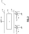
- FIG. 3 depicts a generalized representation of a dual power input plasma system 50.
- Plasma system 50 includes a first electrode 52 connected to a ground 54 and a second electrode 56 spaced apart from first electrode 52.
- power source 60 operates at a second frequency n ⁇ that is the n th harmonic frequency of the frequency of first power source 58.
- power source 60 operates at a frequency that is not a multiple of the frequency of the first power source 58.
- FIG. 4A depicts a schematic block diagram of a power generation system 70 for driving a load.
- Power generation system 70 includes a non-linear load 72, such as a plasma chamber, having electrodes (not shown) powered by a first power generator 74 via a match or matching network 76.
- Non-linear load 72 is also powered by a second power generator 78 via a match or matching network 80.
- power generator 74 is configured as a low frequency RF generator, such as for a bias RF generator
- generator 78 is configured as a high frequency RF generator, such as for a source RF generator.
- match networks 76, 80 may be combined into a single match network, rather than being configured as separate, individual match networks.
- match networks 76, 80 are combined into a single match network, the output from the single match network is input to non-linear load 72.
- both power generators 74, 78 drive the same electrode of non-linear load 72.
- the other electrode of non-linear load 72 may be connected to a ground.
- Power generator 74 includes power controller 84 (Dc(z)) which generates a control signal applied or communicated to power amplifier 86.
- the control signal applied to power amplifier 86 may include one or a plurality of signals to control one or more electrical parameters of power amplifier 86, including voltage, current, frequency, and rail value.
- the control signal applied to power amplifier 86 is an analog signal. The type and content of the control signal may depend on the type of class of the power amplifier 86.
- Power amplifier 86 outputs an amplified signal (DC or RF) to sensor 88.
- Sensor 88 senses the signal output by power amplifier 86 and also passes the amplified power through to match network 76 for application to non-linear load 72.
- Sensor 88 may be configured as an integral or a separate component of power generator 74.
- Sensor 88 generates an output signal, either a voltage and current or a forward and reverse power signal to A/D converter 90.
- A/D converter 90 converts the analog signals received from sensor 88 into digital signals and outputs the digital signal X(n) to scaling module 92, which applies a scaling factor K, and to adaptive rate controller 100.
- Scaling factor K compensates for the sensor output to generate a continuous time, sampled signal.
- the output from scaling module 92 is applied or input to transfer function module 94, represented as D l ( z ), which outputs a signal y representative of the output from power amplifier 86.
- the measured signal y is applied to power controller 84 and to adaptive controller 96.
- Scaling module 92 also communicates with power controller 84 via a communications link which, in various embodiments, enables sharing of internal direct digital synthesizer (DDS) information to enable synchronizing their respective DDSs.
- DDS direct digital synthesizer
- the transfer function D l ( z ) shapes the closed loop control response.
- D l ( z ) provides filtering in order to shift poles and zeros of the closed loop transfer function for the control loop of power generator 74, thereby improving the responsiveness of the control loop.
- D l ( z ) may be implemented in one of a lead filter, lag filter, or lead/lag filter.
- D l ( z ) may be defined as shown below in equation (1):
- D l z K d z ⁇ z 0 z ⁇ z p , z 0 > z p
- Adaptive controller 96 receives as inputs a modeled output signal y m output by reference model 98, and a measured representation y of the output from sensor 88. Adaptive controller 96 receives the two inputs and generates adaptive signals ⁇ 0 and ⁇ 1 for adaptively adjusting operation of power controller 84.
- FIG. 4A also includes an adaptive rate controller 100 which receives as input power setpoint r, which defines at least one electrical parameter to be output by power generator 74, a representation of the control signal from power controller 84, and the signal X(n) from A/D converter 90.
- adaptive rate controller 100 outputs signals to vary the scaling factor K, to thereby adaptively adjust scaling operation of scaling module 92.
- adaptive rate controller 100 receives signals indicative of one or more commanded electrical parameters from other than power controller 84, such as from power generator 78 or another external power generator. In various other embodiments, adaptive rate controller 100 can receive a sensed signal from other than A/D converter 90, such as from power generator 78 or other external power generator.
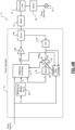
- FIG. 4B depicts a schematic block diagram of another embodiment of a power generation system 71 comprising a power generator 75 for driving the load shown in FIG. 4A .
- the power generation system 71 (specifically the power generator 75) differs from the power generation system 70 (specifically the power generator 74) shown in FIG. 4A in that the power controller 84, D c (z), shown in the power generation system 70 is omitted in the power generation system 71; and a adaptive controller 97 in the power generation system 71 directly receives the input power setpoint r along with power feedback signal (y) and the output of the reference model (y m ).
- the input power setpoint r may be a forward power setpoint or a load leveling setpoint.
- the adaptive controller 97 generates a control signal applied or communicated directly to the power amplifier 86.
- the power generation systems 70 and 71 may be used interchangeably. All other elements of the power generation system 71 operate as described with reference to FIG. 4A and are therefore not described again for brevity.
- FIG. 5A depicts an expanded block diagram of adaptive controller 96.
- Adaptive controller 96 receives a signal y from transfer function D l ( z ) 94 indicating the measured output y of power amplifier 86, such as power, forward power, reverse power, voltage or current.
- Adaptive controller 96 receives a predicted output y m of power amplifier 86 as determined by reference model 98, as will be described in greater detail herein.
- Adaptive controller 96 includes a summer 104 which determines a difference or error e between measured output y and predicted output y m . The error is applied to a pair of multipliers or mixers 106, 108.
- Mixer 106 also receives the predicted output y m so that the predicted output y m is mixed with the error value e.
- the error value e is also input to mixer 108 along with the measured output y so that the error value e and the measured output y are mixed at mixer 108.
- the output from mixer 106 is applied to scalar 110 which applies a scaling value -GammaO to the output from mixer 106.
- the output from mixer 108 is input to scalar 112 which applies a scaling factor Gamma1 to the output from mixer 108.
- Scalars 110 and 112 scale the outputs from the mixers in order to determine a learning rate for adaptive controller 96.
- the output from scalar 110 is input to integrator 114, and the output from scalar 112 is input to integrator 116.
- the output from integrator 114 defines an adaptive rate value ⁇ 0 which is input to power controller 84. As will be described in greater detail herein, ⁇ 0 defines a rate of adjustment of a control signal output to power amplifier 86.
- ⁇ 1 represents an offset to the control signal scaled by ⁇ 0 .
- Gamma0, ⁇ 0 , and ⁇ 0 are used interchangeably and synonymously to denote feedforward path; and Gamma1, ⁇ 1 , and ⁇ 1 are used interchangeably and synonymously to denote feedback path.
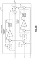
- FIG. 5B depicts another embodiment of the adaptive controller shown as adaptive controller 97.
- the adaptive controller 97 comprises a feedforward network and a feedback network.
- the feedforward network includes elements 106, 110, and 114 described above with reference to FIG. 5A .
- the feedback network includes elements 108, 112, and 116 described above with reference to FIG. 5A .
- the adaptive controllers 96 and 97 may be used interchangeably.
- the feedforward network processes as inputs a filtered version of the input power setpoint r, which is provided by a transfer function 105 (H' m (z)), and an error (e) between the reference model output (y m ) and a system feedback (y).
- the feedback network processes as inputs a filtered version of the following signals, which is provided by a transfer function 107 (H' m (z)): the reference model output (y m ), an error (e) between the reference model output (y m ), and the system feedback (y).
- the transfer function (H' m (z)) is characteristically related to the transfer function (H m (z)) used to implement the reference model 98 and can be set in accordance with the desired operation of the transfer function (H m (z)). In some embodiments, the transfer function (H' m (z)) may not be related to the transfer function (H m (z)).
- Both feedforward and feedback networks form a product from their respective inputs to generate a result that is scaled and integrated.
- the scaling by the feedforward network is performed by - ⁇ 0 (shown as - ⁇ FF).
- the scaling by the feedback network is performed by ⁇ 1 (shown as ⁇ FB ).
- the feedforward network produces the output ⁇ 0 (shown as ⁇ FF ) that is multiplied by the input power setpoint r by a multiplier 109.
- This product i.e., the output of the multiplier 109
- the final result of the adaptive controller 97 i.e., the output of the adder 111 is coupled to drive the input of the power amplifier 86.
- x b log 10 a T
- A is a matrix formed with first columns of log 10 (P i ) and a second unity column.
- ⁇ a recursion is devised around the least square approach.
- a vector x is computed by least squares approximation to describe the ideal power law curve.
- a second least square approximation is built using the actual power readback, P ⁇ l ⁇ i, with the A matrix formed with first columns of log 10 ( P ⁇ l ) ⁇ i and a second unity column.
- the incorporation of a reference model and adaptive model enables a significant feature to the deployed control system.
- the objective of the adaptive controller is to tailor the response of the plant toward the response of the reference model.
- the feedforward path adjusts the setpoint with the power setpoint and the error between the power system feedback and the reference model output. Additionally, the feedback path additively adjusts the setpoint with the power system feedback and the error between the power system feedback and the reference model output. From the information of the reference model and the response of the feedforward and feedback networks, an in-line system identification is formulated.
- FIG. 6 represents a block diagram of power controller Dc(z) 84.
- Power controller 84 receives setpoint r, measured electrical parameter value y, ⁇ 0 , and ⁇ 1 .
- the setpoint r and the measured output y is input to summer 130 which determines an error value e fb applied to a controller 132.
- Controller 132 may be implemented as a proportional-interval-derivative (PID) controller, a state-model controller, or any other controller known in the art.
- Controller 132 generates a control signal u in accordance with the input error e fb .
- the control signal u is mixed with ⁇ 0 at mixer 134.
- ⁇ 0 provides a feedback value for scaling control signal u.
- the scaled value of u is then input to summer 136 which subtracts the value ⁇ 1 from the scaled value to output a control signal u applied to power amplifier 86 of FIG. 4A .
- the value ⁇ 1 provides a feedforward value for offsetting u ⁇ 0 .
- u c u ⁇ 0 + ⁇ 1
- the control signal u c is an adapted representation of u.
- the control system of power generator 74 includes a control loop having an inherent lag or delay between the initiation in a change of a control parameter and the output changing in response to adjusting the control parameter.
- the delay is referred to as a digital group delay, digital delay, or digital analysis delay and is generally defined as the time between initiation of a change and the actual occurrence of the requested change.
- Other delays exist in power generator 74.
- power amplifier 86, sensor 88, and power controller 84 include an inherent delay between receiving an input signal to vary the output of power amplifier 86 and the actual change in the output of power amplifier 86. This delay is referred to as a power supply delay, T PS .
- the power supply delay can be four times greater than the digital group delay.
- control loop can sample the power amplifier output multiple iterations before the power amplifier exhibits a change.
- adaptive controller 96 and adaptive rate controller 100 cooperate to match the system constraints of a digital group delay with the power supply constraints. For example, adaptive controller 96 reduces the digital group delay by generating scaling terms ⁇ 0 and ⁇ 1 to accelerate learning and adjustment of power controller 84.
- Another approach to match the system constraints with the power supply constraints is to adjust the scaling factor K of scaling module 92.
- the scaling factor K of scaling module 92 compensates for the sensed to actual continuous time sampled signals.
- FIG. 7 depicts a plot of frequency versus amplitude of the output from sensor 88 shown as m.
- f s is the setpoint frequency
- f d is a distortion frequency introduced through non-linear load 72, such as by a second power source, such as that applied by power generator 78 in FIG. 4A .
- FIG. 7 depicts a setpoint frequency f s and coupled power about the setpoint frequency f s .
- the coupled power is a power at f d or a different power, such as at f v , as shown in FIG. 7 .
- the coupled power at f d represents distortion power, such as from a second power generator, such as power generator 78.
- f s ⁇ f d and f s ⁇ 2 f d represent intermodular distortion (IMD) between f s and f d .
- the coupled power at f v represents an inherent capacitive or inductive coupling within non-linear load 72.
- ⁇ f defines the bandwidth of the controller, where it is generally desirable to have a bandwidth sufficiently narrow to exclude coupled power, such as K 0 (f) in FIG. 7 .
- setting K determines the bandwidth about the frequency f s for a given K.
- bracket K 0 (f) represents a K 0 (f) having a bandwidth wide enough to detect f s while excluding coupled power.
- the bracket represented by K 1 (f) indicates a K having a bandwidth sufficient to capture f s ⁇ f d
- the bracket K n (f) represents a K having a bandwidth sufficient to capture f s ⁇ 2 f d .
- K 0 (f) represents a slower response or narrower bandwidth than K n (f).
- FIGS. 7 and 8 indicate a benefit of an adaptive rate controller 100 varying K in scaling module 92.
- FIG. 8 represents the output of sensor 88 as a function of time, m(t). As seen in FIG. 8 , m(t) is a step function with the output increasing at t 0 .
- K in scaling module 92 there is a benefit to setting K to K n (f) around t 0 to provide the fastest response and highest bandwidth for detecting the transient at time t 0 .
- the K in scaling module 92 can be set to K 0 since a slower, narrow bandwidth is sufficient to capture variations in m(t) during a steady state.
- K can transition or commutate gradually from K n to K n-1 (t) to K n-2 (t), ... , K 0 , as also shown in FIG. 8.
- FIG. 8 thus represents a possible adaptation of K for a RF continuous wave or DC drive configuration.
- FIG. 9 represents a pulsed DC or pulsed RF waveform m(t) as a function of t.
- K of scaling module 92 can be set to K n (f) to provide the highest bandwidth and best response to detect the transient at these times.
- the scaling factor K can be set to a K having a slower bandwidth, such as K n-1 (t), ... , K 0 .
- K can be commutated between each transient as shown at FIG. 8 . Note that waveform m(t) in FIG.
- time t 4 can define a period
- waveform m(t) can have a period of t 4
- waveform m(t) can vary from period to period, or repeat from period to period.
- the time for a given period of m(t) can vary so that a period is not consistently equal to t 4 .
- the constant K in scaling module 92 can be commutated for each change of setpoint or other property affecting the output of sensor 88.
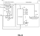
- FIG. 10 depicts adaptive rate controller 140 as an example of adaptive rate controller 100 of FIG. 4A and scaling module 143 as an example of scaling module 92 of FIG. 4A according to various embodiments.
- adaptive rate controller 140 receives as inputs setpoint r, a parameter control output p, which represents a commanded output from power controller 84 to power amplifier 86, and X(n), which in various embodiments is a wideband signal from A/D converter 90.
- setpoint r can represent the setpoint of a control parameter for power generator 74 that may be varied to correspondingly vary the output of power generator 74.
- Setpoint r can represent power, voltage, current, or frequency.
- parameter control output p can be indicative of a control signal for a parameter output by power controller 84 for correspondingly controlling the output of power generator 74, and can include commanded power, voltage, current, frequency, or rail voltage.
- Inputs r and p are input to adaptive rate subsystem controller 142.
- Adaptive rate subsystem controller 142 generates a control signal DDS BW to direct digital synthesizer (DDS) 144 in order to set the frequency of respective cosine and sine signals input to respective mixers 145a, 145b.
- Mixers 145a, 145b also receive X(n), and output respective real components of X(n), X r (n), and imaginary components X i (n) of X(n).
- the output DDS BW of adaptive rate subsystem controller 142 input to DDS 144 is determined in accordance with parameter control output p so that the input signal to DDS 144 is selected such that DDS 144 outputs a frequency in accordance with parameter control output p.
- parameter control output p represents a command frequency output by power controller 84 for power amplifier 86.
- DDS 144 outputs a frequency signal at substantially the same frequency as parameter control output p or with an offset.
- Respective real and imaginary components X r (n), X i (n) are fed back to adaptive rate subsystem controller 142 and processed to track the coupled power, such as described in FIG. 7 to determine the bandwidth ⁇ f .
- US Patent 6707255 assigned to the assignee of the present application, describes various operations of a multirate processing arrangement including a digital frequency synthesizer and mixers for providing real and imaginary components of an input signal.
- K processor 146 receives the X(n) and, in various embodiments, a frequency setpoint signal f DC(z) for setting an output frequency of a DDS in K processor 146, and outputs commutator input (CI) values CI 0r , CI 0i , ..., CI (n-1)r , CI (n-1)i , CI Nr , CI Ni which represent various real and imaginary inputs for commutating K.
- K processor 146 applies various operations to inputs X(n) including filtering, delay, downsampling, and decimation either individually or in combination.
- K processor 146 outputs real and imaginary components.
- the real and imaginary components can be input to a mixer or multiplier, such as mixer or multiplier 147.
- An additional input such as complex value ⁇ n e j ⁇ n , may also be input to mix the real and imaginary components and output a composite CI including both the real and imaginary components.
- Such an approach can be used to combine the real and imaginary components in any of the figures described herein which output individual real and imaginary components of a signal. Mixing with the complex value ⁇ n e j ⁇ n also scales the output to a uniform magnitude and phase response.
- mixing can be considered part of K processor 146 or separate from K processor 146.
- the outputs from K processor 146 are selectively input to commutator 148.
- Commutator 148 selectively switches between CI 0r , CI 0i , ..., CI (n-1)r , CI (n-1)i , CI Nr , CI Ni inputs for output from commutator 148 as a K n value.
- the output from commutator 148 represents a K for scaling module 92.
- Adaptive rate subsystem controller 142 communicates a control signal COM in to commutator 148 to control commutation through the various input signals.
- adaptive rate subsystem controller 142 determines the bandwidth through detecting coupled power, such as IMD, as is well known in the art.
- Coupled power such as IMD
- Examples of determining coupled power, such as IMD can be found in US Patent Application No. 13/834,786, filed March 15, 2013 and entitled Pulse Synchronization by Monitoring Power in Another Frequency Band and US Patent Application No. 15/876189, filed January 21, 2018 and entitled Adaptive Counter Measure Control Thwarting IMD Jamming Impairments for RF Plasma Systems, both owned by the assignee of the present application.
- Adaptive rate controller 140 and scaling module 143 of FIG. 10 describe a generalized representation of adaptive rate controller 100 and scaling module 92 of FIG. 4A .
- various portions of adaptive rate controller 140 and scaling module 92 may be omitted for the purpose of describing that particular figure. However, in various embodiments, such omitted components may still be considered part of the adaptive rate controller described in the respective figure.
- Adaptive rate controller 100, 140 and scaling module 92, 143 affect the commutation of K and the resultant scaling of X(n) in various embodiments.
- commutation can occur using cascaded integrator-comb (CIC) filters to decimate or downsample the output from an A/D converter, such as A/D converter 90.
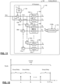
- FIG. 11 shows one various embodiment of scaling module 146 and K processor 150.
- K processor 150 of FIG. 11 is embodied as a digital down converter.
- K processor 150 receives an input signal X(n), such as from A/D converter 90.
- X(n) is split and applied to a pair of mixers 152a, 152b.
- a direct digital synthesizer (DDS) 154 receives an input signal f DC(z) from power controller 84 and generates a sinusoidal signal also applied to respective mixers 152a, 152b.
- foc(z) is a signal that varies with respect to the operating frequency of a DDS in power controller 84, as power controller 84 and scaling module 92 are connected as shown in FIG. 4A .
- the connection of FIG. 4A symbolizes communication so that power controller 84 and scaling module 92 can share and possibly synchronize operating frequency information about their respective DDS.
- f DC(z) may be used directly or offset prior to application or by DDS 154.
- mixer 152a receives from DDS 154 a cosine function signal, such as cos( ⁇ nt) for mixing with X(n) in order to generate a real component of X(n), X r (n).
- DDS 154 generates a sine function signal, such as sin( ⁇ nt) for mixing with X(n) and generate an imaginary component Xi(n) of X(n).
- Respective signals X r (n) and X i (n) are input to respective CIC filters 156a, 156b shown as a first CIC or decimation stage 158.
- CICs 156a, 156b downsample or decimate the respective real and imaginary components of X(n) to generate outputs A r , A i .
- K processor 150 also includes a second CIC or downsampling stage 160 having a pair of CIC filters 162a, 162b.
- Each CIC filter 162a, 162b receives a respective signal X r (n), X i (n) delayed by a predetermined delay Z -1 as shown at respective delay elements 164a, 164b.
- An nth CIC or downsampling stage 168 includes CIC filters 170a, 170b receiving respective signals X r (n) and X i (n) cumulatively delayed by Z -n as shown by the cascaded delay element pairs 164a, 164b and 172a, 172b.
- Second CIC stage 160 outputs respective signals B, and B i
- nth stage delay 168 outputs signals N r and N r
- K processor 150 includes n downsampling or decimation stages, each delayed by a predetermined delay Z -1 through Z -n . Each delay Z -1 may be the same or may vary between each delay element.
- Scaling module 146 also includes a commutator 176 which has a pair of inputs for respectively commutating through outputs A r , A i ; B r , B i ; ..., N r , N i ;. Scaling module 146 thus enables commutation through a series of phase delays starting with zero phase delay through Z -n phase delays.
- FIG. 12 depicts a plot of the interaction between the group delay and the control delay using an adaptive rate controller, such as adaptive rate controller 148 of FIG.11 .
- the x-axis represents the delay n
- the y-axis represents the real component output by commutator 176 of FIG. 11 , which operates as described above with respect to FIG. 10 .
- the group delay between the real components A r , B r , ..., N r are equally spaced in accordance with the delays Z -1 of FIG. 10 .
- the group delays are arranged to synchronize with a power supply delay defined by T GEN or T PS , which is the response time of the generator, such as power generator 74 of FIG. 4A .
- the N group delays fit equally within the power supply group delay.
- the delay Z -1 of FIG. 11 shifts the phase of the commutated K values to match the phase of the control loop for the RF generator T PS , which is substantially defined by the response time from power amplifier 86.
- FIG. 13 depicts a block diagram of one various embodiment of K processor 180 of one various embodiment scaling module 189.
- K processor 180 downsamples or decimates using half-band filters rather than CIC filters of FIG. 11 . Further, rather than cascading delays as in FIG. 11 , K processor 180 cascades downsampling or decimation signals to vary frequency.
- DDS 182 and multipliers 184, 186 operate similarly to those described in FIG. 11 to generate a real component X r (n) and an imaginary component Xi(n). The real and imaginary components X r (n), X i (n) are output without filtering or downsampling at K Nr and K Ni .
- the real and imaginary components X r (n), X i (n) are also split and input to a first half-band stage 190 including respective half-band filters 192a, 192b which provide half-band filtering to respective signals X r (n) and X i (n).
- the half-band filters described herein are conventional half-band filters that operate as low pass filters and that reduce the maximum bandwidth of sample data by an approximate factor of two. Thus, the half-band filters described herein operate as down converters of the respective input signals.
- the output of respective half-band filters 192a, 192b, K (N-1)r and K (N-1)i , respectively, represents downsampled signals of respective input signals X r (n), X i (n) at half the frequency of X r (n) and X i (n).
- the output of respective half-band filters 192a, 192b are input to an additional half-band stage 196 including half-band filters 198a, 198b.
- Half-band filter 198a receives signal K (N-1)r , which has already been downsampled a first time by half-band filter 192a.
- half-band filter 198b receives signal K (N-1)i , which has already been downsampled via half-band filter 192b.
- N half-band filtering stages can be implemented in FIG. 13 to output K 0r and K 0i from stage 196.
- FIG. 13 shows N stages total, including (N-1) downsampled stages and one stage not downsampled to output K Nr , K Ni .
- FIG. 11 effects a phase shift of the respective real and imaginary components of X(n).
- FIG. 13 implements cascaded frequency downsampling or decimation in order to vary K via frequency, rather than phase.
- the outputs of each respective stage are commutated via commutator 200, which operates similarly as described above with respect to FIGS. 10 and 11 scaling module 212 to output a K n in order to vary K.
- FIG. 14 depicts one various embodiment of K processor 210 and scaling module 211, which is configured to commutate both the phase and frequency of K, thereby providing both phase and frequency variation of K.
- K processor 210 includes a digital down converter DDC 212 which may be arranged similarly to scaling module 146 of FIG. 11 .
- the commutated output from digital down converter 212 includes both a real and imaginary components, X r (nRK), X i (nRK). These components represent the output of, for example, commutator 176 of FIG. 11 .
- These components are input to half-band filter section 214, which operates similarly to that described above with respect to K processor 214 of FIG.
- the half-band filter section 214 includes a direct output stage 216, a first downsampled stage 218, and a (N-1) th downsampled stage 220.
- the respective outputs from each stage of half-band down converter 214 are commutated through commutator 220 to output K n .
- digital down converter 212 and half-band filter section 214 combine to implement a K processor, such as generally described at 146 of FIG. 10 .
- K processor 210 of FIG. 14 enables variation of both the phase and the frequency of sampling.
- the digital group delay can be controlled in both phase and frequency to allow improved sampling across the entirety of the control loop.
- FIG. 15 depicts yet another embodiment of a scaling module 230 and K processor 231.
- K processor 231 receives inputs X r (n), X i (n) which are generated as described above in FIGS. 11 and 12 in various embodiments by mixing sine and cosine signals from a DDS with X(n).
- the input X r (n), Xi(n) signals are input to a N stage feedback comb filter to effect downsampling or decimation prior to input to respective frequency dividers 234a, 234b, where N may be any positive integer.
- Frequency dividers 234a, 234b are shown using the frequency dividing term F S a , where a is a predetermined value. For example, a can be any positive integer value.
- the frequency divided signal is output to respective N stage feedforward comb filters 236a, 236b, where N may be any positive integer.
- Comb filters 236a, 236b output respective downsampled, filtered signals K Nr ,
- frequency dividers 234a, 234b The output from frequency dividers 234a, 234b is also input to frequency dividers 240a, 240b which are shown as dividing the input frequency by two. In various embodiments, downsampling or decimation can also occur with a divisor of any positive integer.
- Frequency dividers 242a, 242b output frequency divided signals to respective N stage comb filters 240a, 240b, which in turn output frequency divided, filtered signals K (N-1)r and K (N-1)i .
- a further frequency division/filter stage is provided by respective frequency divider 246a and N stage comb filter 248a for a real component and frequency divider 246b and N stage comb filter 248b for an imaginary component.
- N stage comb filters 248a, 248b output respective K values K (N-2)r , K (N-2)i .
- the frequency division/filtering is repeated down to a final stage to output K 0 .
- frequency dividers 252a, 252b receive respective real and imaginary components and output a further frequency divided signal to respective N stage comb filters 254a, 254b to output respective K values K 0r , K 0i .
- K 0 , K 0r and K 0i are output to a multiplier 258 which also receives as input ⁇ n e j ⁇ n to mix the real and imaginary components and output a composite K 0 including the real and imaginary components.
- a multiplier 258 which also receives as input ⁇ n e j ⁇ n to mix the real and imaginary components and output a composite K 0 including the real and imaginary components.
- K 0 , ... , K N values are commutated via commutator 256, which operates as described above with respect to FIGS. 10 , 11 , 13 , and 14 .
- FIG. 16 depicts a plot of time versus sampling events.
- frequency changes are implemented by simply updating from a first frequency to a second frequency.
- FIG. 16 depicts a chart of time with respect to various sampling events.
- an A/D converter such as A/D converter 90 of FIG. 4A , samples at a rate T A/D .
- A/D converter 90 samples at a rate greater than the digital delay of power generator 74.
- Digital delay sampling events are indicated at T s .
- the frequency change from F INITIAL to F FINAL can be implemented over various increments occurring at the start of one or a combination of an A/D sampling, digital group delay, or power supply delay periods.
- the frequency can be changed in its entirety at any one of a start of a T A/D , T s , and T PS periods.
- the frequency can be changed incrementally at the start of each digital group delay T s period.
- frequency can be adjusted similarly at the start of multiple power supply delays periods T PS over a predetermined number of power supply delays. That is, for example, assuming that it is desirable to change the frequency over M T PS periods, the ⁇ F s can be determined in accordance with ⁇ F s /M so that at each successive start of a power supply delay period, the frequency is incremented by the ⁇ F s / M. Further yet, according to various embodiments, frequency can be updated at various A/D periods T A/D within a one or multiple, predetermined digital group delay periods Ts.
- the frequency can be updated at selected A/D sampling periods T A/D within a given digital group delay period Ts.
- a frequency increment can occur at, for example, every second A/D sampling periods T A/D within a digital group delay periods T s .
- sensor 88 may be a voltage/current probe or a directional coupler. Regardless of whether sensor 88 is a voltage/current probe or a directional coupler, sensor 88 must be calibrated so that its output to power generator 74 can be used for analysis and control.
- Present approaches to calibration of sensors present challenges because the values used for calibration rely on values that create corresponding variability or noise in the resulting calibration determination. In various conventional configuration approaches, the calibration variables not only introduce noise, the calibration variables appear where the noise undesirably propagates through the process. Further, in normal sensor operation, detected values of voltage and current, detected as raw values, must be converted to values meeting National Institute of Standards and Technology (NIST) requirements. In cases of a directional coupler, values must be suitable for conversion to forward and reverse power from NIST voltage and current values. Such calculations require computational overhead, which can add to the group delay of power generator 74.
- NIST National Institute of Standards and Technology
- sensor 88 detects raw voltage and current values that vary as a function of time. That is, sensor 88 detects a raw voltage V raw (t) and a raw current I raw (t).
- the raw voltage and current values must be converted to calibrated values pursuant to NIST standards.
- V c V ⁇ ⁇ I ⁇ Z sc V L Z oc ⁇ Z sc
- v(t) and i(t) are complex quantities generally as defined below with respect to equations (25) and (26).
- equation (28) alleviates a square root function in real time, thereby further minimizing calculations.
- equation (28) determines power provides a much more efficient determination than conventional techniques.
- the calibration approach of equation (28) provides a significantly improved signal to noise ratio during calibration.
- the calibration approach of equation (28) also enables efficient implementation of directional coupler using the output signals from a voltage/current (VI) probe.
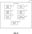
- FIG. 17 shows a control module 270.
- Control module 270 incorporates various components of FIG. 4A .
- Control module 270 may include power control module 272, adaptive control module 274, scaling module 276, adaptive rate module 278, reference module 282, frequency update module 284, and calibration module 286.
- control module 270 includes one or a plurality of processors that execute code associated with the modules 272, 274, 276, 278, 280, 282, and 284. Operation of the modules 272, 274, 276, 278, 280, 282, and 284 is described below with respect to the method of FIG. 18 .
- power controller 84 of FIG. 4A For further defined structure of power controller 84 of FIG. 4A , see the below provided method of FIG. 18 and the below provided definition for the term "module".
- the systems disclosed herein may be operated using numerous methods, an example control system method of which is illustrated in FIG. 18 . Although the following operations are primarily described with respect to the implementations of FIG. 4A , the operations may be easily modified to apply to other implementations of the present disclosure. The operations may be iteratively performed. Although the following operations are shown and primarily described as being performed sequentially, one or more of the following operations may be performed while one or more of the other operations are being performed.
- FIG. 18 depicts a flowchart 290 of power control system controlling the output of a power generator, such as power generator 74 of FIG. 4A or a power generator 75 of FIG. 4B .
- the method begins at 292 in which various initiation and startup processes are executed. Control proceeds either in parallel or sequentially to 294, which determines out-of-band energy from the non-linear load, and to 296, which receives an electrical parameter setpoint for the power generator. Control then proceeds either in parallel or sequentially to one of or all of 298, 300, 302. At 298, the out-of-band energy from the non-linear load and the setpoint are received, and the constant K for scaling a sensed output of the power generator is set. K can be set with input from any of 304, 306, or 308.
- the value K is commutated through phase.
- the K is commutated through frequency.
- K is commutated through both phase and frequency. The set value of K is thus commutated though a series of Ks at 298 for scaling the sensed output of the power generator. K is output to 310.
- 300 determines an estimated output of the power generator based upon the received electrical parameter setpoint.
- Block 300 outputs the estimated power generator output to 312.
- the output of the power generator is sensed, and control proceeds to 310.
- the output of the power generator is scaled in accordance with the constant K output by 298.
- Control then proceeds to 312 which determines an adjustment for the power controller in accordance with the scaled, sensed output and the estimated output of the power generator provided by 300.
- adjustment values are determined and output in order to adjust the response of a power controller at 314.
- Control then proceeds to 316.
- Block 316 updates the frequency at sampling periods at block 318 and generates a control signal to adjust the output of the power amplifier at block 320. Control then proceeds back to blocks 294, 296.
- adaptive rate controller 100 may be implemented in a power generator 74, and reference model 98 and adaptive controller 96 may be omitted from the power generator 74.
- power controller 84 generates a control signal to power amplifier 86 in accordance with power setpoint are and signal y.
- reference model 98 and adaptive controller 96 may be implemented in power generator 74, while adaptive rate controller 100 may be omitted from power generator 74.
- scaling module 92 operates at a fixed value for K. Similar configuration variations are possible with respect to the power generator 75.
- Spatial and functional relationships between elements are described using various terms, including “connected,” “engaged,” “coupled,” “adjacent,” “next to,” “on top of,” “above,” “below,” and “disposed.” Unless explicitly described as being “direct,” when a relationship between first and second elements is described in the above disclosure, that relationship can be a direct relationship where no other intervening elements are present between the first and second elements, but can also be an indirect relationship where one or more intervening elements are present (either spatially or functionally) between the first and second elements.
- the phrase at least one of A, B, and C should be construed to mean a logical (A OR B OR C), using a non-exclusive logical OR, and should not be construed to mean "at least one of A, at least one of B, and at least one of C.”
- the direction of an arrow generally demonstrates the flow of information (such as data or instructions) that is of interest to the illustration.
- information such as data or instructions
- the arrow may point from element A to element B. This unidirectional arrow does not imply that no other information is transmitted from element B to element A.
- element B may send requests for, or receipt acknowledgements of, the information to element A.
- module or the term “controller” may be replaced with the term “circuit.”
- the term “module” may refer to, be part of, or include: an Application Specific Integrated Circuit (ASIC); a digital, analog, or mixed analog/digital discrete circuit; a digital, analog, or mixed analog/digital integrated circuit; a combinational logic circuit; a field programmable gate array (FPGA); a processor circuit (shared, dedicated, or group) that executes code; a memory circuit (shared, dedicated, or group) that stores code executed by the processor circuit; other suitable hardware components that provide the described functionality; or a combination of some or all of the above, such as in a system-on-chip.
- ASIC Application Specific Integrated Circuit
- FPGA field programmable gate array
- the module may include one or more interface circuits.
- the interface circuits may include wired or wireless interfaces that are connected to a local area network (LAN), the Internet, a wide area network (WAN), or combinations thereof.
- LAN local area network
- WAN wide area network
- the functionality of any given module of the present disclosure may be distributed among multiple modules that are connected via interface circuits. For example, multiple modules may allow load balancing.
- a server (also known as remote, or cloud) module may accomplish some functionality on behalf of a client module.
- code may include software, firmware, and/or microcode, and may refer to programs, routines, functions, classes, data structures, and/or objects.
- shared processor circuit encompasses a single processor circuit that executes some or all code from multiple modules.
- group processor circuit encompasses a processor circuit that, in combination with additional processor circuits, executes some or all code from one or more modules. References to multiple processor circuits encompass multiple processor circuits on discrete dies, multiple processor circuits on a single die, multiple cores of a single processor circuit, multiple threads of a single processor circuit, or a combination of the above.
- shared memory circuit encompasses a single memory circuit that stores some or all code from multiple modules.
- group memory circuit encompasses a memory circuit that, in combination with additional memories, stores some or all code from one or more modules.
- the term memory circuit is a subset of the term computer-readable medium.
- the term computer-readable medium does not encompass transitory electrical or electromagnetic signals propagating through a medium (such as on a carrier wave); the term computer-readable medium may therefore be considered tangible and non-transitory.
- Non-limiting examples of a non-transitory, tangible computer-readable medium are nonvolatile memory circuits (such as a flash memory circuit, an erasable programmable read-only memory circuit, or a mask read-only memory circuit), volatile memory circuits (such as a static random access memory circuit or a dynamic random access memory circuit), magnetic storage media (such as an analog or digital magnetic tape or a hard disk drive), and optical storage media (such as a CD, a DVD, or a Blu-ray Disc).
- nonvolatile memory circuits such as a flash memory circuit, an erasable programmable read-only memory circuit, or a mask read-only memory circuit
- volatile memory circuits such as a static random access memory circuit or a dynamic random access memory circuit
- magnetic storage media such as an analog or digital magnetic tape or a hard disk drive
- optical storage media such as a CD, a DVD, or a Blu-ray Disc
- apparatus elements described as having particular attributes or performing particular operations are specifically configured to have those particular attributes and perform those particular operations.
- a description of an element to perform an action means that the element is configured to perform the action.
- the configuration of an element may include programming of the element, such as by encoding instructions on a non-transitory, tangible computer-readable medium associated with the element.
- the apparatuses and methods described in this application may be partially or fully implemented by a special purpose computer created by configuring a general purpose computer to execute one or more particular functions embodied in computer programs.
- the functional blocks, flowchart components, and other elements described above serve as software specifications, which can be translated into the computer programs by the routine work of a skilled technician or programmer.
- the computer programs include processor-executable instructions that are stored on at least one non-transitory, tangible computer-readable medium.
- the computer programs may also include or rely on stored data.
- the computer programs may encompass a basic input/output system (BIOS) that interacts with hardware of the special purpose computer, device drivers that interact with particular devices of the special purpose computer, one or more operating systems, user applications, background services, background applications, etc.
- BIOS basic input/output system
- the computer programs may include: (i) descriptive text to be parsed, such as HTML (hypertext markup language), XML (extensible markup language), or JSON (JavaScript Object Notation) (ii) assembly code, (iii) object code generated from source code by a compiler, (iv) source code for execution by an interpreter, (v) source code for compilation and execution by a just-in-time compiler, etc.
- source code may be written using syntax from languages including C, C++, C#, Objective-C, Swift, Haskell, Go, SQL, R, Lisp, Java ® , Fortran, Perl, Pascal, Curl, OCaml, Javascript ® , HTML5 (Hypertext Markup Language 5th revision), Ada, ASP (Active Server Pages), PHP (PHP: Hypertext Preprocessor), Scala, Eiffel, Smalltalk, Erlang, Ruby, FlashO, Visual Basic ® , Lua, MATLAB, SIMULINK, and Python ® .
Landscapes
- Physics & Mathematics (AREA)
- Engineering & Computer Science (AREA)
- Plasma & Fusion (AREA)
- Chemical & Material Sciences (AREA)
- Analytical Chemistry (AREA)
- General Physics & Mathematics (AREA)
- Automation & Control Theory (AREA)
- Amplifiers (AREA)
- Plasma Technology (AREA)
- Drying Of Semiconductors (AREA)
Description
- This application claims priority to
U.S. Patent Application No. 16/297,799, filed on March 11, 2019 U.S. Provisional Application No. 62/690,202, filed on June 26, 2018 - The present disclosure relates to power generation and to controlling power generation in systems driving non-linear loads.
- The background description provided herein is for the purpose of generally presenting the context of the disclosure. Work of the presently named inventors, to the extent the work is described in this background section, as well as aspects of the description that may not otherwise qualify as prior art at the time of filing, are neither expressly nor impliedly admitted as prior art against the present disclosure.
- Plasma etching is frequently used in semiconductor fabrication. In plasma etching, ions are accelerated by an electric field to etch exposed surfaces on a substrate. In one basic implementation, the electric field is generated based on Radio Frequency (RF) or Direct Current (DC) power signals generated by a respective RF or DC generator of a power delivery system. The power signals generated by the generator must be precisely controlled to effectively execute plasma etching.
WO 2017/204889 A1 ,US 2006/126367 A1 andJP 2001 137214 A - A power generator comprises a power amplifier. The power amplifier generates a power signal communicated to a non-linear load in accordance with an input control signal. A power controller communicates the input control signal to the power amplifier. An adaptive controller generates at least one adjustment value communicated to the power controller to adjust responsiveness of the power controller. The at least one adjustment value includes one of a feedback and a feedforward component.
- A power generator comprises an adaptive controller and a power amplifier. The adaptive controller generates a control signal based on an input setpoint for the power generator to generate a power signal, a measured representation of the power signal, and a modeled representation of the power signal. The control signal includes a feedback component and a feedforward component. The power amplifier generates the power signal communicated to a non-linear load in accordance with the control signal.
- An adaptive controller comprises a feedforward circuit, a feedback circuit, and a combiner. The feedforward circuit generates a feedforward signal based on an input setpoint for a power generator to generate a power signal and based on a difference between a measured representation of the power signal and a modeled representation of the power signal. The feedback circuit generating a feedback signal based on the difference between the measured representation of the power signal and the modeled representation of the power signal. The combiner generates a control signal by combining the feedforward signal and the feedback signal. The control signal enables the power generator to generate the power signal communicated to a non-linear load.
- An adaptive rate controller comprises a direct digital synthesizer, a first mixer, a second mixer, and a subsystem controller. The direct digital synthesizer generates a sinusoidal signal and a cosine signal based on a control signal. The first mixer mixes the sinusoidal signal and a digital representation of a power signal generated by a power generator and generating a real component of the digital representation of the power signal. The second mixer mixes the cosine signal and the digital representation of the power signal and generating an imaginary component of the digital representation of the power signal. The subsystem controller generating the control signal based on the real and imaginary components, an input setpoint for the power generator to generate the power signal, and a parameter used to control the power signal.
- A power generator comprises a power amplifier, a power controller, and an adaptive controller. The power amplifier generates a power signal communicated to a non-linear load in accordance with an input control signal. The power controller communicates the input control signal to the power amplifier. The adaptive controller generates at least one adjustment value communicated to the power controller to adjust responsiveness of the power controller. The at least one adjustment value includes one of a feedback component and a feedforward component.
- A method comprises generating a control signal based on an input setpoint for a power generator to generate a power signal, a measured representation of the power signal, and a modeled representation of the power signal. The control signal includes a feedback component and a feedforward component. The method further comprises generating the power signal communicated to a non-linear load in accordance with the control signal. The method further comprises generating the feedforward component based on the input setpoint and a difference between the measured representation of the power signal and the modeled representation of the power signal. The method further comprises generating the feedback component based the difference between the measured representation of the power signal and the modeled representation of the power signal. The method further comprises generating an output to adaptively scale the measured representation of the power signal based on at least one of the input setpoint, the measured representation of the power signal, and the control signal. The method further comprises generating the control signal based on the adaptively scaled measured representation of the power signal. The method further comprises generating an output to adaptively scale the measured representation of the power signal based on commutating by at least one of phase, frequency, or both phase and frequency.
- Further areas of applicability of the present disclosure will become apparent from the detailed description, the claims and the drawings. The detailed description and specific examples are intended for purposes of illustration only and are not intended to limit the scope of the disclosure. The invention is defined by the claims.
-
-
FIG. 1 depicts a representation of an inductively coupled plasma system; -
FIG. 2 depicts a representation of a capacitively coupled plasma system; -
FIG. 3 depicts a generalized representation of a plasma system arranged according to various embodiments of the present disclosure; -
FIG. 4A is a schematic block diagram of a power generation system for driving a non-linear load; -
FIG. 4B is a schematic block diagram of another embodiment of the power generation system ofFIG. 4A ; -
FIG. 5A is a schematic block diagram of the adaptive controller ofFIG. 4A according to various embodiments; -
FIG. 5B is a schematic block diagram of another embodiment of the adaptive controller ofFIG. 4B ; -
FIG. 6 is a schematic block diagram of the power controller ofFIG. 4A according to various embodiments; -
FIG. 7 depicts a frequency plot of a predetermined operating frequency and intermodulation distortion (IMD) frequencies resulting from distortion frequencies for a power generation system; -
FIG. 8 is a waveform of an example signal output by the power generator ofFIGS. 4A and4B ; -
FIG. 9 is an example waveform of a variable signal output by the power generator ofFIGS. 4A and4B ; -
FIG. 10 is a schematic block diagram of an adaptive rate controller and scaling module ofFIGS. 4A and4B according to various embodiments; -
FIG. 11 is a schematic block diagram of portions of the scaling module ofFIGS. 4A and4B according to various embodiments; -
FIG. 12 is a plot of a relationship between example commutated outputs ofFIG. 11 and a group delay and a control loop delay of a power generator; -
FIG. 13 is a schematic block diagram of portions of the scaling module ofFIGS. 4A and4B according to various embodiments; -
FIG. 14 is a schematic block diagram of portions of the scaling module ofFIGS. 4A and4B according to various embodiments; -
FIG. 15 is a schematic block diagram of portions of the scaling module ofFIGS. 4A and4B according to various embodiments; -
FIG. 16 is a plot of time versus sampling events to illustrate various frequency approaches; -
FIG. 17 is a functional block diagram of an example control module in accordance with various embodiments of the present disclosure; and -
FIG. 18 is a flow chart for controlling a power controller according to various embodiments. - In the drawings, reference numbers may be reused to identify similar and/or identical elements.
- Throughout the specification, power generator may refer to a DC power generator or a RF power generator.
- A power system may include a DC or RF power generator, a matching network, and a load (e.g., a plasma chamber). The power generator generates a DC or RF power signal, which is received by the matching network or impedance optimizing controller or circuit. The matching network or impedance optimizing controller or circuit matches an input impedance of the matching network to a characteristic impedance of a transmission line between the power generator and the matching network. This impedance matching aids in maximizing an amount of power forwarded to the matching network ("forward power") and minimizing an amount of power reflected back from the matching network to the power generator ("reverse power"). Forward power may be maximized and reverse power may be minimized when the input impedance of the matching network matches the characteristic impedance of the transmission line.
- In the power source or power supply field, there are typically two approaches to applying a power signal to the load. A first, more traditional approach is to apply a continuous power signal to the load. In a continuous mode, a continuous power signal is typically a constant DC or RF sinusoidal power signal that is output continuously by the power source to the load. In the continuous mode approach, the power signal assumes a constant DC or sinusoidal output, and the amplitude of the power signal and/or frequency (of a RF power signal) can be varied in order to vary the output power applied to the load.
- A second approach to applying the power signal to the load involves pulsing the power signal, rather than applying a continuous power signal to the load. In a pulse mode of operation, a power signal is modulated by a modulation signal in order to define an envelope for the modulated power signal. In a conventional pulse modulation scheme, the power signal typically remains at a constant amplitude and, for RF signals, a constant frequency. Power delivered to the load is varied by varying the modulation signal, rather than varying the power signal.
- In a typical power supply configuration, output power applied to the load is determined by using sensors that measure the forward and reflected power or the voltage and current of the RF signal applied to the load. Either set of these signals is analyzed in a control loop. The analysis typically determines a power value which is used to adjust the output of the power supply in order to vary the power applied to the load. In a power delivery system where the load is a plasma chamber or other non-linear load, the varying impedance of the load causes a corresponding varying of power applied to the load, as applied power is in part a function of the impedance of the load.
- In plasma systems, power is typically delivered in one of two configurations. In a first configuration, the power is capacitively coupled to the plasma chamber. Such systems are referred to as capacitively coupled plasma (CCP) systems. In a second configuration, the power is inductively coupled to the plasma chamber. Such systems are typically referred to as inductively coupled plasma (ICP) systems. Plasma delivery systems typically include a bias power and a source power applied to one or a plurality of electrodes. The source power typically generates the plasma and controls plasma density, and the bias power modulates ions in the formulation of a sheath of plasma. The bias and the source may share the same electrode or may use separate electrodes, in accordance with various design considerations.
- When a power delivery system drives a non-linear load, such as a plasma chamber, the power absorbed by the plasma sheath results in a density of ions with a range of ion energy. One characteristic measure of ion energy is the ion energy distribution function (IEDF). The ion energy distribution function (IEDF) can be controlled with the bias power. One way of controlling the IEDF for a system in which multiple RF power signals are applied to the load occurs by varying multiple RF signals that are related by frequency and phase. The frequencies between the multiple RF power signals may be locked, and the relative phase between the multiple RF signals may also be locked. Examples of such systems can be found with reference to
US Patent No. 7,602,127 ,US Patent No. 8,110,991 , andUS Patent No. 8,395,322 , all assigned to the assignee of the present application. - Plasma processing systems may also include components for plasma generation and control. One such component is a non-linear load, such as a plasma chamber or reactor. A typical plasma chamber or reactor utilized in plasma processing systems, such as by way of example, for thin-film manufacturing, can utilize a dual frequency system. One power generator (the source) controls the generation of the plasma, and the power generator (the bias) controls ion energy. Examples of dual power systems include systems that are described in
US Patent No. 7,602,127 ;US Patent No. 8,110,991 ; andUS Patent No. 8,395,322 , referenced above. The dual power system described in the above-referenced patents requires a closed-loop control system to adapt power supply operation for the purpose of controlling ion density and its corresponding ion energy distribution function (IEDF). - Multiple approaches exist for controlling a plasma chamber for generating plasmas. For example, in RF power delivery systems, phase and frequency of the driving RF signals may be used to control plasma generation. For RF driven plasma sources, the periodic waveform affecting plasma sheath dynamics and the corresponding ion energy are generally known and are controlled by the frequency of the periodic waveforms and the associated phase interaction. Another approach in RF power delivery systems involves dual frequency control. That is, two RF frequency sources are used to power a plasma chamber to provide substantially independent control of ion and electron densities.
- Another approach utilizes wideband RF power sources to drive a plasma chamber. A wideband approach presents certain challenges. One challenge is coupling the power to the electrode. A second challenge is that the transfer function of the generated waveform to the actual sheath voltage for a desired IEDF must be formulated for a wide-process space to support material surface interaction. In one responsive approach in an inductively coupled plasma system, controlling power applied to a source electrode controls the plasma density while controlling power applied to the bias electrode modulates ions to control the IEDF to provide etch rate control. By using source electrode and bias electrode control, the etch rate is controlled via the ion density and energy.
- As integrated device fabrication continues to evolve, so do the power requirements for controlling the plasma for device fabric fabrication. For example, for memory device fabrication, the requirements for bias power continue to increase. Increased power generates higher energetic ions for faster surface interaction, thereby increasing the etch rate. Increased bias power is sometimes accompanied by, in RF systems, a lower bias frequency requirement along with an increase in the number of bias power sources coupled to the plasma sheath created in the plasma chamber. The increased power at a lower bias frequency and the increased number of bias power sources results in intermodulation distortion (IMD) emissions from a sheath modulation. The IMD emissions can significantly reduce power delivered by the source where plasma generation occurs.
U.S. Patent Application No. 13/834,786, filed March 15, 2013 -
FIG. 1 depicts an exemplary representation of an inductively coupled plasma (ICP)system 10.ICP system 10 includes a non-linear load, such as aplasma chamber 12, which will be referred to interchangeably herein, for generatingplasma 14. Power in the form of voltage or current is applied toplasma chamber 12 via a pair of coils, including a coil assembly that in various embodiments includes aninner coil 16 and anouter coil 18. Power is applied toinner coil 16 via a RF power generator orpower source 20, and power is applied toouter coil 18 via RF power generator orpower source 22.Coils dielectric window 24 that assists in coupling power toplasma chamber 12. A substrate 26 is placed inplasma chamber 12 and typically forms the work piece that is the subject of plasma operations. A RF power generator, power supply or power source 28 (the terms may be used herein interchangeably) applies power toplasma chamber 12 via substrate 26. In various configurations, thepower sources plasma 14 or control the plasma density. Also in various configurations,power source 28 provides a bias voltage or current that modulates the ions to control the ion energy or ion density of theplasma 14. In various embodiments,power sources power sources -
FIG. 2 depicts an exemplary representation of a capacitively coupled plasma (CCP)system 30.CCP system 30 includes aplasma chamber 32 for generatingplasma 34. A pair ofelectrodes plasma chamber 32 connect to respective DC (ω=0) or RF power generators orpower sources power source 40 provides a source voltage or current to ignite or generateplasma 34 or control the plasma density. Also in various embodiments,power source 42 provides a bias voltage or current that modulates the ions in the plasma to control the ion energy and/or ion density of theplasma 34. In various RF embodiments,power sources power sources power sources -
FIG. 3 depicts a generalized representation of a dual powerinput plasma system 50.Plasma system 50 includes afirst electrode 52 connected to a ground 54 and asecond electrode 56 spaced apart fromfirst electrode 52. A first DC (ω=0) orRF power source 58 generates a first RF power applied tosecond electrode 56 at a first frequency f. Asecond power source 60 generates a second DC (ω=0) or RF power applied tosecond electrode 56. In various embodiments,power source 60 operates at a second frequency nω that is the nth harmonic frequency of the frequency offirst power source 58. In various other embodiments,power source 60 operates at a frequency that is not a multiple of the frequency of thefirst power source 58. -
FIG. 4A depicts a schematic block diagram of apower generation system 70 for driving a load.Power generation system 70 includes anon-linear load 72, such as a plasma chamber, having electrodes (not shown) powered by afirst power generator 74 via a match or matchingnetwork 76.Non-linear load 72 is also powered by asecond power generator 78 via a match or matchingnetwork 80. As shown inFIG. 4A , for RF power applications,power generator 74 is configured as a low frequency RF generator, such as for a bias RF generator, andgenerator 78 is configured as a high frequency RF generator, such as for a source RF generator. - In various embodiments,
match networks non-linear load 72. In such a configuration, bothpower generators non-linear load 72. In various embodiments, the other electrode ofnon-linear load 72 may be connected to a ground. -
Power generator 74 includes power controller 84 (Dc(z)) which generates a control signal applied or communicated topower amplifier 86. The control signal applied topower amplifier 86 may include one or a plurality of signals to control one or more electrical parameters ofpower amplifier 86, including voltage, current, frequency, and rail value. The control signal applied topower amplifier 86 is an analog signal. The type and content of the control signal may depend on the type of class of thepower amplifier 86.Power amplifier 86 outputs an amplified signal (DC or RF) tosensor 88.Sensor 88 senses the signal output bypower amplifier 86 and also passes the amplified power through to matchnetwork 76 for application tonon-linear load 72.Sensor 88 may be configured as an integral or a separate component ofpower generator 74.Sensor 88 generates an output signal, either a voltage and current or a forward and reverse power signal to A/D converter 90. A/D converter 90 converts the analog signals received fromsensor 88 into digital signals and outputs the digital signal X(n) to scalingmodule 92, which applies a scaling factor K, and toadaptive rate controller 100. Scaling factor K compensates for the sensor output to generate a continuous time, sampled signal. The output from scalingmodule 92 is applied or input totransfer function module 94, represented as Dl (z), which outputs a signal y representative of the output frompower amplifier 86. The measured signal y is applied topower controller 84 and toadaptive controller 96.Scaling module 92 also communicates withpower controller 84 via a communications link which, in various embodiments, enables sharing of internal direct digital synthesizer (DDS) information to enable synchronizing their respective DDSs. - The transfer function Dl (z) shapes the closed loop control response. In various embodiments Dl (z) provides filtering in order to shift poles and zeros of the closed loop transfer function for the control loop of
power generator 74, thereby improving the responsiveness of the control loop. Dl (z) may be implemented in one of a lead filter, lag filter, or lead/lag filter. In various embodiments, Dl (z) may be defined as shown below in equation (1):
- z 0 is a zero of Dl (z); and
- zp is a pole of Dl (z).
-
Adaptive controller 96 receives as inputs a modeled output signal ym output byreference model 98, and a measured representation y of the output fromsensor 88.Adaptive controller 96 receives the two inputs and generates adaptive signals θ 0 and θ 1 for adaptively adjusting operation ofpower controller 84.FIG. 4A also includes anadaptive rate controller 100 which receives as input power setpoint r, which defines at least one electrical parameter to be output bypower generator 74, a representation of the control signal frompower controller 84, and the signal X(n) from A/D converter 90. As will be described in greater detail herein,adaptive rate controller 100 outputs signals to vary the scaling factor K, to thereby adaptively adjust scaling operation of scalingmodule 92. In various embodiments,adaptive rate controller 100 receives signals indicative of one or more commanded electrical parameters from other thanpower controller 84, such as frompower generator 78 or another external power generator. In various other embodiments,adaptive rate controller 100 can receive a sensed signal from other than A/D converter 90, such as frompower generator 78 or other external power generator. -
FIG. 4B depicts a schematic block diagram of another embodiment of apower generation system 71 comprising apower generator 75 for driving the load shown inFIG. 4A . The power generation system 71 (specifically the power generator 75) differs from the power generation system 70 (specifically the power generator 74) shown inFIG. 4A in that thepower controller 84, Dc(z), shown in thepower generation system 70 is omitted in thepower generation system 71; and aadaptive controller 97 in thepower generation system 71 directly receives the input power setpoint r along with power feedback signal (y) and the output of the reference model (ym). The input power setpoint r may be a forward power setpoint or a load leveling setpoint. Theadaptive controller 97 generates a control signal applied or communicated directly to thepower amplifier 86. Throughout the disclosure, thepower generation systems power generation system 71 operate as described with reference toFIG. 4A and are therefore not described again for brevity. -
FIG. 5A depicts an expanded block diagram ofadaptive controller 96.Adaptive controller 96 receives a signal y from transfer function Dl (z) 94 indicating the measured output y ofpower amplifier 86, such as power, forward power, reverse power, voltage or current.Adaptive controller 96 receives a predicted output ym ofpower amplifier 86 as determined byreference model 98, as will be described in greater detail herein.Adaptive controller 96 includes asummer 104 which determines a difference or error e between measured output y and predicted output ym. The error is applied to a pair of multipliers ormixers Mixer 106 also receives the predicted output ym so that the predicted output ym is mixed with the error value e. The error value e is also input tomixer 108 along with the measured output y so that the error value e and the measured output y are mixed atmixer 108. -
Reference model 98 simulates the desired plant dynamics of the system using a transfer function Hm (z) as described below in equation (2):
- Y(z) is the reference model system transfer function output; and
- R(z) is the reference model system transfer function input.
- The output from
mixer 106 is applied to scalar 110 which applies a scaling value -GammaO to the output frommixer 106. Similarly, the output frommixer 108 is input to scalar 112 which applies a scaling factor Gamma1 to the output frommixer 108.Scalars adaptive controller 96. The output fromscalar 110 is input tointegrator 114, and the output fromscalar 112 is input tointegrator 116. The output fromintegrator 114 defines an adaptive rate value θ 0 which is input topower controller 84. As will be described in greater detail herein, θ 0 defines a rate of adjustment of a control signal output topower amplifier 86. The output fromscalar 112 is input tointegrator 116 which outputs an integrated value tomixer 120.Mixer 120 mixes the integrated value output fromintegrator 116 with the measured output y to generate θ 1. As will be described in greater detail herein, θ 1 represents an offset to the control signal scaled by θ 0. Throughout the disclosure, Gamma0, γ0, and θ 0 are used interchangeably and synonymously to denote feedforward path; and Gamma1, γ1, and θ 1 are used interchangeably and synonymously to denote feedback path. -
FIG. 5B depicts another embodiment of the adaptive controller shown asadaptive controller 97. Theadaptive controller 97 comprises a feedforward network and a feedback network. The feedforward network includeselements FIG. 5A . The feedback network includeselements FIG. 5A . Throughout the disclosure, theadaptive controllers - In
FIG. 5B , the feedforward network processes as inputs a filtered version of the input power setpoint r, which is provided by a transfer function 105 (H'm(z)), and an error (e) between the reference model output (ym) and a system feedback (y). The feedback network processes as inputs a filtered version of the following signals, which is provided by a transfer function 107 (H'm(z)): the reference model output (ym), an error (e) between the reference model output (ym), and the system feedback (y). The transfer function (H'm(z)) is characteristically related to the transfer function (Hm(z)) used to implement thereference model 98 and can be set in accordance with the desired operation of the transfer function (Hm(z)). In some embodiments, the transfer function (H'm(z)) may not be related to the transfer function (Hm(z)). - Both feedforward and feedback networks form a product from their respective inputs to generate a result that is scaled and integrated. The scaling by the feedforward network is performed by -γ0 (shown as -γFF). The scaling by the feedback network is performed by γ1 (shown as γFB). The feedforward network produces the output θ0 (shown as θFF) that is multiplied by the input power setpoint r by a
multiplier 109. This product (i.e., the output of the multiplier 109) is added to the output of the feedback network θ1 (shown as θFB) by anadder 111. The final result of the adaptive controller 97 (i.e., the output of the adder 111) is coupled to drive the input of thepower amplifier 86. - In the
adaptive controller 97, there are scalars assigned to the feedforward and feedback networks. While the scalars can take on different values, for computational efficiencies, preferred values are for γ0=γ1. In this case, note that γ=γ0=γ1. The determination of this scalar drives the learning rates for the respective networks. An online recursion process is used to tailor the response for an optimal adaption rate, γ. - For a power amplifier, the gain of the learning rate follows a power law curve, γ=aPb, where P represent the power setpoint, and where a and b are parameters describing the power response. Applying logic10 to the function γ=aPb yields the following Equation (3):

i denotes the sampled power law curve function's data points.
By least squares, the above equation can be solved for optimal parameters a and b using Equation (4):

A is a matrix formed with first columns of log10(Pi) and a second unity column. - To determine the best adaption rate, γ, a recursion is devised around the least square approach. First, a vector x is computed by least squares approximation to describe the ideal power law curve. A second least square approximation is built using the actual power readback, P̂l ∀i, with the A matrix formed with first columns of log10(P̂l ) ∀i and a second unity column.
- By least square, the power law curve parameters are estimated using the Equation (5):


- An error function, ê, is formed from the power law curve generated by:




g is a gain parameter scaling the error to the new parameterized power law curve Cnew.
This new power law curve function is parameterized by least square using the following Equation (10):


x is continually improved. - The incorporation of a reference model and adaptive model enables a significant feature to the deployed control system. The objective of the adaptive controller is to tailor the response of the plant toward the response of the reference model. The feedforward path adjusts the setpoint with the power setpoint and the error between the power system feedback and the reference model output. Additionally, the feedback path additively adjusts the setpoint with the power system feedback and the error between the power system feedback and the reference model output. From the information of the reference model and the response of the feedforward and feedback networks, an in-line system identification is formulated. A continuous time, second order plant transfer function with a zero has a discrete time describing transfer by the following Equation (12):




-
FIG. 6 represents a block diagram of power controller Dc(z) 84.Power controller 84 receives setpoint r, measured electrical parameter value y, θ 0, and θ 1. The setpoint r and the measured output y is input tosummer 130 which determines an error value efb applied to acontroller 132.Controller 132 may be implemented as a proportional-interval-derivative (PID) controller, a state-model controller, or any other controller known in the art.Controller 132 generates a control signal u in accordance with the input error efb. The control signal u is mixed with θ 0 atmixer 134. Thus, θ 0 provides a feedback value for scaling control signal u. The scaled value of u is then input tosummer 136 which subtracts the value θ 1 from the scaled value to output a control signal u applied topower amplifier 86 ofFIG. 4A . The value θ 1 provides a feedforward value for offsetting uθ 0. Thus, uc = uθ 0 + θ 1, and the control signal uc is an adapted representation of u. - In various embodiments, the control system of
power generator 74 includes a control loop having an inherent lag or delay between the initiation in a change of a control parameter and the output changing in response to adjusting the control parameter. The delay is referred to as a digital group delay, digital delay, or digital analysis delay and is generally defined as the time between initiation of a change and the actual occurrence of the requested change. Other delays exist inpower generator 74. For example,power amplifier 86,sensor 88, andpower controller 84 include an inherent delay between receiving an input signal to vary the output ofpower amplifier 86 and the actual change in the output ofpower amplifier 86. This delay is referred to as a power supply delay, TPS. In fact, in various configurations, the power supply delay can be four times greater than the digital group delay. While a digital group delay of less than the power supply delay is generally desirable, such a difference presents certain challenges and opportunities. In particular, with a group delay less than the power supply delay, the control loop can sample the power amplifier output multiple iterations before the power amplifier exhibits a change. - In various embodiments,
adaptive controller 96 andadaptive rate controller 100 cooperate to match the system constraints of a digital group delay with the power supply constraints. For example,adaptive controller 96 reduces the digital group delay by generating scaling terms θ 0 and θ 1 to accelerate learning and adjustment ofpower controller 84. Another approach to match the system constraints with the power supply constraints is to adjust the scaling factor K of scalingmodule 92. In various embodiments, the scaling factor K of scalingmodule 92 compensates for the sensed to actual continuous time sampled signals. -
FIG. 7 depicts a plot of frequency versus amplitude of the output fromsensor 88 shown as m. InFIG. 7 fs is the setpoint frequency and fd is a distortion frequency introduced throughnon-linear load 72, such as by a second power source, such as that applied bypower generator 78 inFIG. 4A .FIG. 7 depicts a setpoint frequency fs and coupled power about the setpoint frequency fs. The coupled power is a power at fd or a different power, such as at fv, as shown inFIG. 7 . The coupled power at fd represents distortion power, such as from a second power generator, such aspower generator 78. Thus, fs ± fd and fs ± 2fd represent intermodular distortion (IMD) between fs and fd. The coupled power at fv represents an inherent capacitive or inductive coupling withinnon-linear load 72. Note that Δf defines the bandwidth of the controller, where it is generally desirable to have a bandwidth sufficiently narrow to exclude coupled power, such as K0(f) inFIG. 7 . - Referring to scaling
module 92 ofFIG. 4A and toFIG. 7 , setting K determines the bandwidth about the frequency fs for a given K. For example, bracket K0(f) represents a K0(f) having a bandwidth wide enough to detect fs while excluding coupled power. Similarly, the bracket represented by K1(f) indicates a K having a bandwidth sufficient to capture fs ± fd, and the bracket Kn(f) represents a K having a bandwidth sufficient to capture fs ± 2fd. In terms of response, K0(f) represents a slower response or narrower bandwidth than Kn(f). -
FIGS. 7 and 8 indicate a benefit of anadaptive rate controller 100 varying K in scalingmodule 92.FIG. 8 represents the output ofsensor 88 as a function of time, m(t). As seen inFIG. 8 , m(t) is a step function with the output increasing at t0. With reference to adapting the constant K in scalingmodule 92, there is a benefit to setting K to Kn(f) around t0 to provide the fastest response and highest bandwidth for detecting the transient at time t0. Following the transient t0, the K in scalingmodule 92 can be set to K0 since a slower, narrow bandwidth is sufficient to capture variations in m(t) during a steady state. In various embodiments, K can transition or commutate gradually from Kn to Kn-1(t) to Kn-2(t), ... , K0, as also shown inFIG. 8. FIG. 8 thus represents a possible adaptation of K for a RF continuous wave or DC drive configuration. -
FIG. 9 represents a pulsed DC or pulsed RF waveform m(t) as a function of t. At each transition t0, t1, t2, t3, and t4, K of scalingmodule 92 can be set to Kn(f) to provide the highest bandwidth and best response to detect the transient at these times. Between the time t0, t1, ... , t4, the scaling factor K can be set to a K having a slower bandwidth, such as Kn-1(t), ... , K0. InFIG. 9 , K can be commutated between each transient as shown atFIG. 8 . Note that waveform m(t) inFIG. 9 can be a repeating pulse with transitions occurring at t0, t1, t2, t3, and t4. In various embodiments, time t4 can define a period, and waveform m(t) can have a period of t4. In various other embodiments, waveform m(t) can vary from period to period, or repeat from period to period. In various other embodiments, the time for a given period of m(t) can vary so that a period is not consistently equal to t4. - Thus, from
FIGS. 8 and 9 , the constant K in scalingmodule 92 can be commutated for each change of setpoint or other property affecting the output ofsensor 88. -
FIG. 10 depictsadaptive rate controller 140 as an example ofadaptive rate controller 100 ofFIG. 4A and scalingmodule 143 as an example of scalingmodule 92 ofFIG. 4A according to various embodiments. As described above with respect toFIG. 4A ,adaptive rate controller 140 receives as inputs setpoint r, a parameter control output p, which represents a commanded output frompower controller 84 topower amplifier 86, and X(n), which in various embodiments is a wideband signal from A/D converter 90. In various embodiments, setpoint r can represent the setpoint of a control parameter forpower generator 74 that may be varied to correspondingly vary the output ofpower generator 74. Setpoint r can represent power, voltage, current, or frequency. Likewise, parameter control output p can be indicative of a control signal for a parameter output bypower controller 84 for correspondingly controlling the output ofpower generator 74, and can include commanded power, voltage, current, frequency, or rail voltage. - Inputs r and p are input to adaptive
rate subsystem controller 142. Adaptiverate subsystem controller 142 generates a control signal DDSBW to direct digital synthesizer (DDS) 144 in order to set the frequency of respective cosine and sine signals input torespective mixers Mixers rate subsystem controller 142 input toDDS 144 is determined in accordance with parameter control output p so that the input signal toDDS 144 is selected such thatDDS 144 outputs a frequency in accordance with parameter control output p. In various embodiments, parameter control output p represents a command frequency output bypower controller 84 forpower amplifier 86.DDS 144 outputs a frequency signal at substantially the same frequency as parameter control output p or with an offset. Respective real and imaginary components Xr(n), Xi(n) are fed back to adaptiverate subsystem controller 142 and processed to track the coupled power, such as described inFIG. 7 to determine the bandwidth Δf.US Patent 6707255 , assigned to the assignee of the present application, describes various operations of a multirate processing arrangement including a digital frequency synthesizer and mixers for providing real and imaginary components of an input signal. - As will be described in greater detail below,
K processor 146 receives the X(n) and, in various embodiments, a frequency setpoint signal fDC(z) for setting an output frequency of a DDS inK processor 146, and outputs commutator input (CI) values CI0r, CI0i, ..., CI(n-1)r, CI(n-1)i, CINr, CINi which represent various real and imaginary inputs for commutating K. In various embodiments,K processor 146 applies various operations to inputs X(n) including filtering, delay, downsampling, and decimation either individually or in combination. In various embodiments,K processor 146 outputs real and imaginary components. In various other embodiments, however, the real and imaginary components can be input to a mixer or multiplier, such as mixer ormultiplier 147. An additional input, such as complex value αnejϕn, may also be input to mix the real and imaginary components and output a composite CI including both the real and imaginary components. Such an approach can be used to combine the real and imaginary components in any of the figures described herein which output individual real and imaginary components of a signal. Mixing with the complex value αnejϕn also scales the output to a uniform magnitude and phase response. Although shown external toK processor 146 for descriptive purposes, mixing can be considered part ofK processor 146 or separate fromK processor 146. - The outputs from
K processor 146 are selectively input tocommutator 148.Commutator 148 selectively switches between CI0r, CI0i, ..., CI(n-1)r, CI(n-1)i, CINr, CINi inputs for output fromcommutator 148 as a Kn value. As will be recognized, if a pair of real and imaginary components are mixed, such as shown atmixer 147, only a single value is commutated viacommutator 148. The output fromcommutator 148 represents a K for scalingmodule 92. Adaptiverate subsystem controller 142 communicates a control signal COMin tocommutator 148 to control commutation through the various input signals.Subsystem controller 142 determines the signal COMin in accordance with Δf described above. Particularly, Δf = min(|fs ± nfd |,fv ). Further, COMin varies as described below:
rate subsystem controller 142 determines the bandwidth through detecting coupled power, such as IMD, as is well known in the art. Examples of determining coupled power, such as IMD, can be found inUS Patent Application No. 13/834,786, filed March 15, 2013 US Patent Application No. 15/876189, filed January 21, 2018 -
Adaptive rate controller 140 andscaling module 143 ofFIG. 10 describe a generalized representation ofadaptive rate controller 100 and scalingmodule 92 ofFIG. 4A . In various figures described throughout the specification, various portions ofadaptive rate controller 140 and scalingmodule 92 may be omitted for the purpose of describing that particular figure. However, in various embodiments, such omitted components may still be considered part of the adaptive rate controller described in the respective figure. -
Adaptive rate controller module D converter 90.FIG. 11 shows one various embodiment of scalingmodule 146 andK processor 150.K processor 150 ofFIG. 11 is embodied as a digital down converter.K processor 150 receives an input signal X(n), such as from A/D converter 90. X(n) is split and applied to a pair ofmixers power controller 84 and generates a sinusoidal signal also applied torespective mixers power controller 84, aspower controller 84 and scalingmodule 92 are connected as shown inFIG. 4A . The connection ofFIG. 4A symbolizes communication so thatpower controller 84 and scalingmodule 92 can share and possibly synchronize operating frequency information about their respective DDS. In various embodiments, fDC(z) may be used directly or offset prior to application or byDDS 154. In various embodiments,mixer 152a receives from DDS 154 a cosine function signal, such as cos(ωnt) for mixing with X(n) in order to generate a real component of X(n), Xr(n). In various embodiments,DDS 154 generates a sine function signal, such as sin(ωnt) for mixing with X(n) and generate an imaginary component Xi(n) of X(n). - Respective signals Xr(n) and Xi(n) are input to
respective CIC filters decimation stage 158.CICs stage 160 having a pair ofCIC filters CIC filter respective delay elements stage 168 includesCIC filters Second CIC stage 160 outputs respective signals B, and Bi , andnth stage delay 168 outputs signals Nr and Nr Thus,K processor 150 includes n downsampling or decimation stages, each delayed by a predetermined delay Z-1 through Z-n. Each delay Z-1 may be the same or may vary between each delay element.Scaling module 146 also includes acommutator 176 which has a pair of inputs for respectively commutating through outputs Ar, Ai ; Br, Bi ; ..., Nr, Ni ;.Scaling module 146 thus enables commutation through a series of phase delays starting with zero phase delay through Z-n phase delays. -
FIG. 12 depicts a plot of the interaction between the group delay and the control delay using an adaptive rate controller, such asadaptive rate controller 148 ofFIG.11 . InFIG. 12 , the x-axis represents the delay n, and the y-axis represents the real component output bycommutator 176 ofFIG. 11 , which operates as described above with respect toFIG. 10 . As shown inFIG. 12 , the group delay between the real components Ar, Br, ..., Nr are equally spaced in accordance with the delays Z-1 ofFIG. 10 . The group delays are arranged to synchronize with a power supply delay defined by TGEN or TPS, which is the response time of the generator, such aspower generator 74 ofFIG. 4A . As shown, the N group delays fit equally within the power supply group delay. Thus, as shown inFIG. 12 , the delay Z-1 ofFIG. 11 shifts the phase of the commutated K values to match the phase of the control loop for the RF generator TPS, which is substantially defined by the response time frompower amplifier 86. -
FIG. 13 depicts a block diagram of one various embodiment ofK processor 180 of one variousembodiment scaling module 189.K processor 180 downsamples or decimates using half-band filters rather than CIC filters ofFIG. 11 . Further, rather than cascading delays as inFIG. 11 ,K processor 180 cascades downsampling or decimation signals to vary frequency.DDS 182 and multipliers 184, 186 operate similarly to those described inFIG. 11 to generate a real component Xr(n) and an imaginary component Xi(n). The real and imaginary components Xr(n), Xi(n) are output without filtering or downsampling at KNr and KNi. - The real and imaginary components Xr(n), Xi(n) are also split and input to a first half-
band stage 190 including respective half-band filters band filters band filters band stage 196 including half-band filters band filter 198a receives signal K(N-1)r, which has already been downsampled a first time by half-band filter 192a. Similarly, half-band filter 198b receives signal K(N-1)i, which has already been downsampled via half-band filter 192b. N half-band filtering stages can be implemented inFIG. 13 to output K0r and K0i fromstage 196. For example,FIG. 13 shows N stages total, including (N-1) downsampled stages and one stage not downsampled to output KNr, KNi. - With reference to
FIG. 11 andFIG. 13 ,FIG. 11 effects a phase shift of the respective real and imaginary components of X(n).FIG. 13 , on the other hand, implements cascaded frequency downsampling or decimation in order to vary K via frequency, rather than phase. The outputs of each respective stage are commutated viacommutator 200, which operates similarly as described above with respect toFIGS. 10 and11 scaling module 212 to output a Kn in order to vary K. -
FIG. 14 depicts one various embodiment ofK processor 210 andscaling module 211, which is configured to commutate both the phase and frequency of K, thereby providing both phase and frequency variation ofK. K processor 210 includes a digitaldown converter DDC 212 which may be arranged similarly to scalingmodule 146 ofFIG. 11 . The commutated output fromdigital down converter 212 includes both a real and imaginary components, Xr(nRK), Xi(nRK). These components represent the output of, for example,commutator 176 ofFIG. 11 . These components are input to half-band filter section 214, which operates similarly to that described above with respect toK processor 214 ofFIG. 13 withoutDDS 182 andmixers FIG. 13 . The half-band filter section 214 includes adirect output stage 216, a firstdownsampled stage 218, and a (N-1)thdownsampled stage 220. The respective outputs from each stage of half-band downconverter 214 are commutated throughcommutator 220 to output Kn. Thus,digital down converter 212 and half-band filter section 214 combine to implement a K processor, such as generally described at 146 ofFIG. 10 . - With reference to
FIG. 12 ,K processor 210 ofFIG. 14 enables variation of both the phase and the frequency of sampling. Thus, the digital group delay can be controlled in both phase and frequency to allow improved sampling across the entirety of the control loop. -
FIG. 15 depicts yet another embodiment of ascaling module 230 andK processor 231.K processor 231 receives inputs Xr(n), Xi(n) which are generated as described above inFIGS. 11 and 12 in various embodiments by mixing sine and cosine signals from a DDS with X(n). The input Xr(n), Xi(n) signals are input to a N stage feedback comb filter to effect downsampling or decimation prior to input torespective frequency dividers Frequency dividers 
feedforward comb filters Comb filters - The output from
frequency dividers frequency dividers 240a, 240b which are shown as dividing the input frequency by two. In various embodiments, downsampling or decimation can also occur with a divisor of any positive integer.Frequency dividers stage comb filters 240a, 240b, which in turn output frequency divided, filtered signals K(N-1)r and K(N-1)i. A further frequency division/filter stage is provided byrespective frequency divider 246a and Nstage comb filter 248a for a real component andfrequency divider 246b and Nstage comb filter 248b for an imaginary component. Nstage comb filters - In the final stage,
frequency dividers stage comb filters multiplier 258 which also receives as input αnejϕn to mix the real and imaginary components and output a composite K0 including the real and imaginary components. As described above, such an approach can be used to combine the real and imaginary components in any of the figures described herein which output individual real and imaginary components of a signal. The K0, ... , KN values are commutated viacommutator 256, which operates as described above with respect toFIGS. 10 ,11 ,13 , and14 . -
FIG. 16 depicts a plot of time versus sampling events. In a typical power generator, frequency changes are implemented by simply updating from a first frequency to a second frequency. Conventionally, little regard is paid to the timing of frequency changes with respect to sampling events or the magnitude of the adjustment. With reference toFIG. 16, FIG. 16 depicts a chart of time with respect to various sampling events. For example, an A/D converter, such as A/D converter 90 ofFIG. 4A , samples at a rate TA/D. In various configurations, A/D converter 90 samples at a rate greater than the digital delay ofpower generator 74. Digital delay sampling events are indicated at Ts. In various configurations, it is generally desirable to have multiple A/D sampling events within a given digital group delay in order to improve signal to noise ratio and overall accuracy. Further, and as discussed above, multiple digital group delays can occur within the power generator or power supply delay TPG. This is shown also inFIG. 16 in which N=4, where four digital group delays Ts occur within one power generator delay TPG. - Further, in various power generator control implementations, it is known to increment the frequency from a first frequency to a second frequency using servo control to increment from the first frequency to the second frequency. An example of such incremental control can be found with respect to
U.S. Patent Nos. 8,576,013 and8,781,415 , assigned to the Assignee of the present application. One approach to incrementing the frequency setpoint from Fs(k) to Fs(k+1) can be found below with equation (17):
- G is a transfer function to determine the frequency increment;
- γ is a PID controller coefficient;
- β is a PID controller coefficient; and
- di (k), di (k - 1), and di (k - 2) are the distortion values measured at the kth, (k-1)th, and (k-2)th increments.
- Accordingly, there are multiple approaches to effect such frequency updating. For example, assuming that the initial frequency is FINITIAL and the final frequency is FFINAL and that the Δfs = FFINAL - FINITIAL. This frequency change from FINITIAL to FFINAL can be implemented over various increments occurring at the start of one or a combination of an A/D sampling, digital group delay, or power supply delay periods. For example, according to various embodiments, the frequency can be changed in its entirety at any one of a start of a TA/D, Ts, and TPS periods. Alternatively, and according to various embodiments, the frequency can be changed incrementally at the start of each digital group delay Ts period. That is, for N digital group delays in one power supply delay, increment at the start of each period Ts is by ΔFs /N. According to various other embodiments, frequency can be adjusted similarly at the start of multiple power supply delays periods TPS over a predetermined number of power supply delays. That is, for example, assuming that it is desirable to change the frequency over M TPS periods, the ΔFs can be determined in accordance with ΔFs /M so that at each successive start of a power supply delay period, the frequency is incremented by the ΔFs /M. Further yet, according to various embodiments, frequency can be updated at various A/D periods TA/D within a one or multiple, predetermined digital group delay periods Ts. Further yet, the frequency can be updated at selected A/D sampling periods TA/D within a given digital group delay period Ts. By way of non-limiting example, a frequency increment can occur at, for example, every second A/D sampling periods TA/D within a digital group delay periods Ts.
- Referring to the block diagram of
FIG. 4A , in various embodiments,sensor 88 may be a voltage/current probe or a directional coupler. Regardless of whethersensor 88 is a voltage/current probe or a directional coupler,sensor 88 must be calibrated so that its output topower generator 74 can be used for analysis and control. Present approaches to calibration of sensors present challenges because the values used for calibration rely on values that create corresponding variability or noise in the resulting calibration determination. In various conventional configuration approaches, the calibration variables not only introduce noise, the calibration variables appear where the noise undesirably propagates through the process. Further, in normal sensor operation, detected values of voltage and current, detected as raw values, must be converted to values meeting National Institute of Standards and Technology (NIST) requirements. In cases of a directional coupler, values must be suitable for conversion to forward and reverse power from NIST voltage and current values. Such calculations require computational overhead, which can add to the group delay ofpower generator 74. - In operation,
sensor 88 detects raw voltage and current values that vary as a function of time. That is,sensor 88 detects a raw voltage Vraw(t) and a raw current Iraw(t). The raw voltage and current values must be converted to calibrated values pursuant to NIST standards. For example, equation (19) below indicates the calibration equation:
-
y is a matrix calibrated values of voltage and current; -
a is a matrix of values for converting the raw voltages to calibrated voltages; and -
x is a matrix of raw, uncalibrated values. - v(t) and i(t) are the calibrated, respective voltage and current as a function of time;
- Vraw (t) and iraw (t) are the raw voltage and current values detected by the sensor;
- Vc is as defined below;
- Ic is as defined below;
- Zoc is the open circuit impedance of the sensor; and
- Zsc is the short circuit impedance of the sensor.
- Vc is defined below with respect to equation (21):

-
V is the raw voltage measured during the 50 ohm portion of VI sensor calibration; -
I is the raw current measured during the 50 ohm portion of the VI sensor calibration; - Zoc and Zsc are as described above with respect to equation (20);
- ZL is the low impedance measurement provided by the NIST traceable impedance transfer standards; and
- VL is the voltage measurement provided by the NIST traceable power transfer standards.
- Further, v(t) and i(t) are complex quantities generally as defined below with respect to equations (25) and (26).


- ω is the frequency;
- t is time; and
- ϕv and ϕi are the respective phases for the voltage and current.
- Note that the squared term in equation (28) alleviates a square root function in real time, thereby further minimizing calculations. Thus, relying on equation (28) to determine power provides a much more efficient determination than conventional techniques. Further by removing the term (Zoc - Zsc ) from the denominators of equations (21), (22), and (27), the calibration approach of equation (28) provides a significantly improved signal to noise ratio during calibration. The calibration approach of equation (28) also enables efficient implementation of directional coupler using the output signals from a voltage/current (VI) probe.
-
FIG. 17 shows acontrol module 270.Control module 270 incorporates various components ofFIG. 4A .Control module 270 may include power control module 272,adaptive control module 274, scalingmodule 276,adaptive rate module 278,reference module 282,frequency update module 284, and calibration module 286. In various embodiments,control module 270 includes one or a plurality of processors that execute code associated with themodules modules FIG. 18 . - For further defined structure of
power controller 84 ofFIG. 4A , see the below provided method ofFIG. 18 and the below provided definition for the term "module". The systems disclosed herein may be operated using numerous methods, an example control system method of which is illustrated inFIG. 18 . Although the following operations are primarily described with respect to the implementations ofFIG. 4A , the operations may be easily modified to apply to other implementations of the present disclosure. The operations may be iteratively performed. Although the following operations are shown and primarily described as being performed sequentially, one or more of the following operations may be performed while one or more of the other operations are being performed. -
FIG. 18 depicts aflowchart 290 of power control system controlling the output of a power generator, such aspower generator 74 ofFIG. 4A or apower generator 75 ofFIG. 4B . The method begins at 292 in which various initiation and startup processes are executed. Control proceeds either in parallel or sequentially to 294, which determines out-of-band energy from the non-linear load, and to 296, which receives an electrical parameter setpoint for the power generator. Control then proceeds either in parallel or sequentially to one of or all of 298, 300, 302. At 298, the out-of-band energy from the non-linear load and the setpoint are received, and the constant K for scaling a sensed output of the power generator is set. K can be set with input from any of 304, 306, or 308. At 304, the value K is commutated through phase. At 306, the K is commutated through frequency. At 308, K is commutated through both phase and frequency. The set value of K is thus commutated though a series of Ks at 298 for scaling the sensed output of the power generator. K is output to 310. - Returning to 300, 300 determines an estimated output of the power generator based upon the received electrical parameter setpoint. Block 300 outputs the estimated power generator output to 312. At 302, the output of the power generator is sensed, and control proceeds to 310. At 310 the output of the power generator is scaled in accordance with the constant K output by 298. Control then proceeds to 312 which determines an adjustment for the power controller in accordance with the scaled, sensed output and the estimated output of the power generator provided by 300. At 312, adjustment values are determined and output in order to adjust the response of a power controller at 314. Control then proceeds to 316. Block 316 updates the frequency at sampling periods at
block 318 and generates a control signal to adjust the output of the power amplifier atblock 320. Control then proceeds back toblocks - Note that in various embodiments,
adaptive rate controller 100 may be implemented in apower generator 74, andreference model 98 andadaptive controller 96 may be omitted from thepower generator 74. In such a configuration,power controller 84 generates a control signal topower amplifier 86 in accordance with power setpoint are and signal y. Similarly, in various embodiments,reference model 98 andadaptive controller 96 may be implemented inpower generator 74, whileadaptive rate controller 100 may be omitted frompower generator 74. In such a configuration, scalingmodule 92 operates at a fixed value for K. Similar configuration variations are possible with respect to thepower generator 75. - The foregoing description is merely illustrative in nature and is in no way intended to limit the disclosure, its application, or uses. The broad teachings of the disclosure can be implemented in a variety of forms. Therefore, while this disclosure includes particular examples, the true scope of the disclosure should not be so limited since other modifications will become apparent upon a study of the drawings, the specification, and the following claims. It should be understood that one or more steps within a method may be executed in different order (or concurrently) without altering the principles of the present disclosure.
- Spatial and functional relationships between elements (for example, between modules, circuit elements, semiconductor layers, etc.) are described using various terms, including "connected," "engaged," "coupled," "adjacent," "next to," "on top of," "above," "below," and "disposed." Unless explicitly described as being "direct," when a relationship between first and second elements is described in the above disclosure, that relationship can be a direct relationship where no other intervening elements are present between the first and second elements, but can also be an indirect relationship where one or more intervening elements are present (either spatially or functionally) between the first and second elements. As used herein, the phrase at least one of A, B, and C should be construed to mean a logical (A OR B OR C), using a non-exclusive logical OR, and should not be construed to mean "at least one of A, at least one of B, and at least one of C."
- In the figures, the direction of an arrow, as indicated by the arrowhead, generally demonstrates the flow of information (such as data or instructions) that is of interest to the illustration. For example, when element A and element B exchange a variety of information but information transmitted from element A to element B is relevant to the illustration, the arrow may point from element A to element B. This unidirectional arrow does not imply that no other information is transmitted from element B to element A. Further, for information sent from element A to element B, element B may send requests for, or receipt acknowledgements of, the information to element A.
- In this application, including the definitions below, the term "module" or the term "controller" may be replaced with the term "circuit." The term "module" may refer to, be part of, or include: an Application Specific Integrated Circuit (ASIC); a digital, analog, or mixed analog/digital discrete circuit; a digital, analog, or mixed analog/digital integrated circuit; a combinational logic circuit; a field programmable gate array (FPGA); a processor circuit (shared, dedicated, or group) that executes code; a memory circuit (shared, dedicated, or group) that stores code executed by the processor circuit; other suitable hardware components that provide the described functionality; or a combination of some or all of the above, such as in a system-on-chip.
- The module may include one or more interface circuits. In some examples, the interface circuits may include wired or wireless interfaces that are connected to a local area network (LAN), the Internet, a wide area network (WAN), or combinations thereof. The functionality of any given module of the present disclosure may be distributed among multiple modules that are connected via interface circuits. For example, multiple modules may allow load balancing. In a further example, a server (also known as remote, or cloud) module may accomplish some functionality on behalf of a client module.
- The term code, as used above, may include software, firmware, and/or microcode, and may refer to programs, routines, functions, classes, data structures, and/or objects. The term shared processor circuit encompasses a single processor circuit that executes some or all code from multiple modules. The term group processor circuit encompasses a processor circuit that, in combination with additional processor circuits, executes some or all code from one or more modules. References to multiple processor circuits encompass multiple processor circuits on discrete dies, multiple processor circuits on a single die, multiple cores of a single processor circuit, multiple threads of a single processor circuit, or a combination of the above. The term shared memory circuit encompasses a single memory circuit that stores some or all code from multiple modules. The term group memory circuit encompasses a memory circuit that, in combination with additional memories, stores some or all code from one or more modules.
- The term memory circuit is a subset of the term computer-readable medium. The term computer-readable medium, as used herein, does not encompass transitory electrical or electromagnetic signals propagating through a medium (such as on a carrier wave); the term computer-readable medium may therefore be considered tangible and non-transitory. Non-limiting examples of a non-transitory, tangible computer-readable medium are nonvolatile memory circuits (such as a flash memory circuit, an erasable programmable read-only memory circuit, or a mask read-only memory circuit), volatile memory circuits (such as a static random access memory circuit or a dynamic random access memory circuit), magnetic storage media (such as an analog or digital magnetic tape or a hard disk drive), and optical storage media (such as a CD, a DVD, or a Blu-ray Disc).
- In this application, apparatus elements described as having particular attributes or performing particular operations are specifically configured to have those particular attributes and perform those particular operations. Specifically, a description of an element to perform an action means that the element is configured to perform the action. The configuration of an element may include programming of the element, such as by encoding instructions on a non-transitory, tangible computer-readable medium associated with the element.
- The apparatuses and methods described in this application may be partially or fully implemented by a special purpose computer created by configuring a general purpose computer to execute one or more particular functions embodied in computer programs. The functional blocks, flowchart components, and other elements described above serve as software specifications, which can be translated into the computer programs by the routine work of a skilled technician or programmer.
- The computer programs include processor-executable instructions that are stored on at least one non-transitory, tangible computer-readable medium. The computer programs may also include or rely on stored data. The computer programs may encompass a basic input/output system (BIOS) that interacts with hardware of the special purpose computer, device drivers that interact with particular devices of the special purpose computer, one or more operating systems, user applications, background services, background applications, etc.
- The computer programs may include: (i) descriptive text to be parsed, such as HTML (hypertext markup language), XML (extensible markup language), or JSON (JavaScript Object Notation) (ii) assembly code, (iii) object code generated from source code by a compiler, (iv) source code for execution by an interpreter, (v) source code for compilation and execution by a just-in-time compiler, etc. As examples only, source code may be written using syntax from languages including C, C++, C#, Objective-C, Swift, Haskell, Go, SQL, R, Lisp, Java®, Fortran, Perl, Pascal, Curl, OCaml, Javascript®, HTML5 (Hypertext Markup Language 5th revision), Ada, ASP (Active Server Pages), PHP (PHP: Hypertext Preprocessor), Scala, Eiffel, Smalltalk, Erlang, Ruby, FlashO, Visual Basic®, Lua, MATLAB, SIMULINK, and Python®.




Claims (15)
- A power generator (74, 75), comprising:an adaptive controller (96, 97) configured to generate a control signal based on an input setpoint for the power generator (74, 75) to generate a power signal, a measured representation of the power signal, and a modeled representation of the power signal, wherein the control signal includes a feedback component and a feedforward component; anda power amplifier (86) configured to generate the power signal communicated to a non-linear load in accordance with the control signal.
- The power generator (74, 75) of claim 1, wherein the adaptive controller (96, 97) comprises:a feedforward circuit (Gamma0, γ0, and θ0) configured to generate the feedforward component based on the input setpoint and a difference between the measured representation of the power signal and the modeled representation of the power signal; anda feedback circuit (Gamma1, γ1, and θ 1) configured to generate the feedback component based on the difference between the measured representation of the power signal and the modeled representation of the power signal.
- The power generator (74, 75) of claim 1 or 2, further comprising an adaptive rate controller (100) configured to determine the measured representation of the power signal based on the input setpoint, the measured representation of the power signal, and the control signal.
- The power generator (74, 75) of any preceding claim, further comprising an adaptive rate controller (100) configured to generate an output to adaptively scale the measured representation of the power signal based on at least one of the input setpoint, the measured representation of the power signal, and the control signal, wherein the adaptive controller generates the control signal based on the adaptively scaled measured representation of the power signal.
- The power generator (74, 75) of any of claims 1 to 3, further comprising an adaptive rate controller (100) configured to generate an output to adaptively scale the measured representation of the power signal based on commutating by at least one of phase, frequency, or both phase and frequency.
- A system (70, 71) comprising the power generator (74, 75) of claim 1, and further comprising:
an adaptive rate controller (100), comprising:a direct digital synthesizer (144, 154, 182) configured to generate a sinusoidal signal and a cosine signal based on a second control signal;a first mixer (145a, 152a, 184a) configured to mix the sinusoidal signal and a digital representation of the power signal, and to generate a real component of the digital representation of the power signal;a second mixer (145b, 152b, 184b) configured to mix the cosine signal and the digital representation of the power signal, and to generate an imaginary component of the digital representation of the power signal; anda subsystem controller (142) configured to generate the second control signal based on the real and imaginary components, the input setpoint for the power generator, and a parameter used to control the power signal. - The system of claim 6, wherein the subsystem controller (142) is configured to generate an output to adaptively scale the measured representation of the power signal, and wherein the adaptively scaled measured representation of the power signal is used to generate the parameter that is used to control the power signal.
- The system of claim 6 or 7, further comprising a scaling circuit (143, 146, 189, 2311, 230) configured to adaptively scale the measured representation of the power signal, wherein the adaptively scaled measured representation of the power signal is used to generate the parameter that is used to control the power signal.
- The system of any of claims 6 to 8, wherein the subsystem controller (142) is configured to generate an output signal to adaptively scale the measured representation of the power signal, the system further comprising:a processor (146, 150, 180, 210, 231) configured to process the digital representation of the power signal, and to generate a plurality of real and imaginary components; anda commutator (148, 176, 200, 220, 256) configured to selectively switch between the plurality of real and imaginary components based on the output signal to output a scaling factor to adaptively scale the measured representation of the power signal.
- The system of any of claims 6 to 9, wherein the subsystem controller (142) is configured to generate an output signal to adaptively scale the measured representation of the power signal, the system further comprising:a processor (146, 150, 180, 210, 231) configured to process the digital representation of the power signal, generating a plurality of real and imaginary components, and to generate a composite value by combining a pair of the real and imaginary components and a complex value; anda commutator (148, 176, 200, 256) configured to selectively switch between the composite value and the plurality of real and imaginary components based on the output signal to output a scaling factor to adaptively scale the measured representation of the power signal.
- A method, comprising:generating a control signal (320) based on an input setpoint for a power generator (296) to generate a power signal, a measured representation (302) of the power signal, and a modelled representation (300) of the power signal, wherein the control signal (320) includes a feedback component and a feedforward component; andgenerating the power signal communicated to a non-linear load in accordance with the control signal.
- The method of claim 11, further comprising:generating the feedforward component (Gamma0, γ0, and θ 0) based on the input setpoint and a difference between the measured representation (302) of the power signal and the modelled representation (300) of the power signal; andgenerating the feedback component (Gamma1, γ1, and θ 1) based on the difference between the measured representation (302) of the power signal and the modelled representation (300) of the power signal.
- The method of claim 11 or 12, further comprising determining the measured representation of the power signal (302) based on the input setpoint, the measured representation of the power signal, and the control signal.
- The method of any of claims 11 to 13, further comprising:generating an output to adaptively scale the measured representation of the power signal (310, 312, 314) based on at least one of the input setpoint, the measured representation of the power signal, and the control signal; andgenerating the control signal (320) based on the adaptively scaled measured representation of the power signal.
- The method of any of claims 11 to 13, further comprising generating an output to adaptively scale the measured representation of the power signal (310, 312, 314) based on commutating by at least one of phase, frequency, or both phase and frequency.
Applications Claiming Priority (3)
| Application Number | Priority Date | Filing Date | Title |
|---|---|---|---|
| US201862690202P | 2018-06-26 | 2018-06-26 | |
| US16/297,799 US11042140B2 (en) | 2018-06-26 | 2019-03-11 | Adaptive control for a power generator |
| PCT/US2019/038730 WO2020005832A1 (en) | 2018-06-26 | 2019-06-24 | Adaptive control for a power generator |
Publications (3)
| Publication Number | Publication Date |
|---|---|
| EP3815126A1 EP3815126A1 (en) | 2021-05-05 |
| EP3815126A4 EP3815126A4 (en) | 2022-03-30 |
| EP3815126B1 true EP3815126B1 (en) | 2023-06-14 |
Family
ID=68981741
Family Applications (1)
| Application Number | Title | Priority Date | Filing Date |
|---|---|---|---|
| EP19825918.6A Active EP3815126B1 (en) | 2018-06-26 | 2019-06-24 | Adaptive control for a power generator |
Country Status (8)
| Country | Link |
|---|---|
| US (2) | US11042140B2 (en) |
| EP (1) | EP3815126B1 (en) |
| JP (1) | JP7074876B2 (en) |
| KR (1) | KR102364185B1 (en) |
| CN (1) | CN111954916B (en) |
| SG (1) | SG11202008409QA (en) |
| TW (1) | TWI750482B (en) |
| WO (1) | WO2020005832A1 (en) |
Families Citing this family (28)
| Publication number | Priority date | Publication date | Assignee | Title |
|---|---|---|---|---|
| US12205796B2 (en) | 2019-07-31 | 2025-01-21 | Lam Research Corporation | Radio frequency power generator having multiple output ports |
| CN112616320B (en) * | 2019-08-05 | 2024-04-05 | 株式会社日立高新技术 | Plasma treatment device |
| US10741363B1 (en) * | 2019-10-08 | 2020-08-11 | Mks Instruments, Inc. | Extremum seeking control apparatus and method for automatic frequency tuning for RF impedance matching |
| CN114762079B (en) | 2019-12-02 | 2025-02-28 | 朗姆研究公司 | Impedance transformation in RF-assisted plasma generation |
| US12626895B2 (en) | 2020-03-27 | 2026-05-12 | Lam Research Corporation | RF signal parameter measurement in an integrated circuit fabrication chamber |
| CN116075917A (en) * | 2020-06-12 | 2023-05-05 | 朗姆研究公司 | Control of Plasma Formation by RF Coupling Structures |
| US11527384B2 (en) * | 2020-11-24 | 2022-12-13 | Mks Instruments, Inc. | Apparatus and tuning method for mitigating RF load impedance variations due to periodic disturbances |
| CN113381617B (en) | 2021-06-29 | 2024-10-18 | 昂宝电子(上海)有限公司 | Constant voltage switching power supply and control chip and method thereof |
| US11715624B2 (en) * | 2021-08-09 | 2023-08-01 | Mks Instruments, Inc. | Adaptive pulse shaping with post match sensor |
| CN117280446A (en) | 2021-08-23 | 2023-12-22 | 株式会社日立高新技术 | Plasma processing device and plasma processing method |
| US11721523B2 (en) * | 2021-09-07 | 2023-08-08 | Advanced Energy Industries, Inc. | Control of rail voltage in multi-level pulsing RF power amplifier |
| US12080530B2 (en) * | 2021-09-13 | 2024-09-03 | Advanced Energy Industries, Inc | Model reference adaptive control with signum projection tensor operations |
| US11972926B2 (en) * | 2021-10-05 | 2024-04-30 | Advanced Energy Industries, Inc. | Dynamic control-setpoint modification |
| US12300464B2 (en) | 2021-10-25 | 2025-05-13 | Advanced Energy Industries, Inc. | Robust tensorized shaped setpoint waveform streaming control |
| TWI779965B (en) * | 2021-12-14 | 2022-10-01 | 瑞昱半導體股份有限公司 | Measuring system and associated method |
| US12142461B2 (en) * | 2022-05-05 | 2024-11-12 | Applied Materials, Inc. | Control and prediction of multiple plasma coupling surfaces and corresponding power transfer |
| CN115036202B (en) * | 2022-06-29 | 2025-08-26 | 北京北方华创微电子装备有限公司 | A voltage control method for lower radio frequency power supply and semiconductor process equipment |
| US12197174B2 (en) * | 2022-06-30 | 2025-01-14 | Advanced Energy Industries, Inc. | Adaptive engine with sliding mode predictor |
| US12394597B2 (en) * | 2022-06-30 | 2025-08-19 | Advanced Energy Industries, Inc. | Adaptive engine with estimation law modules for plasma processing power system |
| US12314016B2 (en) | 2022-06-30 | 2025-05-27 | Advanced Energy Industries, Inc. | Plasma processing control system with adaptive fuzzy controller |
| US12607974B2 (en) * | 2022-06-30 | 2026-04-21 | Advanced Energy Industries, Inc. | Adaptive engine with pre-processed control laws |
| US12393166B2 (en) | 2022-06-30 | 2025-08-19 | Advanced Energy Industries, Inc. | Adaptive PID controller |
| US12306597B2 (en) | 2022-06-30 | 2025-05-20 | Advanced Energy Industries, Inc. | Adaptive engine with bifurcated nonlinear model |
| US12386321B2 (en) | 2022-06-30 | 2025-08-12 | Advanced Energy Industries, Inc. | Adaptive engine for tracking and regulation control using a control law selector and combiner |
| US20240055228A1 (en) * | 2022-08-10 | 2024-02-15 | Mks Instruments, Inc. | Plasma Process Control of Multi-Electrode Systems Equipped with Ion Energy Sensors |
| US12278090B2 (en) | 2023-04-18 | 2025-04-15 | Mks Instruments, Inc. | Enhanced tuning methods for mitigating RF load impedance variations due to periodic disturbances |
| US20250087462A1 (en) * | 2023-09-08 | 2025-03-13 | Applied Materials, Inc. | Radio-frequency (rf) matching network and tuning technique |
| CN121143097B (en) * | 2025-07-24 | 2026-04-17 | 广东工业大学 | Nonlinear multi-autonomous system fixed time consistency control method, device and medium |
Family Cites Families (25)
| Publication number | Priority date | Publication date | Assignee | Title |
|---|---|---|---|---|
| US5604468A (en) * | 1996-04-22 | 1997-02-18 | Motorola, Inc. | Frequency synthesizer with temperature compensation and frequency multiplication and method of providing the same |
| JP2003505817A (en) * | 1999-07-23 | 2003-02-12 | シーゲイト テクノロジー エルエルシー | Disturbance rejection for disk drives using adaptive accelerometer feedforward servo |
| JP2001137214A (en) * | 1999-11-12 | 2001-05-22 | Hitachi Medical Corp | Power supply device and magnetic resonance imaging apparatus using the same |
| US6707255B2 (en) | 2002-07-10 | 2004-03-16 | Eni Technology, Inc. | Multirate processing for metrology of plasma RF source |
| US7755300B2 (en) * | 2003-09-22 | 2010-07-13 | Mks Instruments, Inc. | Method and apparatus for preventing instabilities in radio-frequency plasma processing |
| US7289341B2 (en) * | 2004-12-14 | 2007-10-30 | Advanced Energy Industries, Inc. | Power supply adaptive feedforward control circuit |
| US7474149B2 (en) * | 2005-03-25 | 2009-01-06 | Pulsewave Rf, Inc. | Radio frequency power amplifier and method using a controlled supply |
| US7602127B2 (en) | 2005-04-18 | 2009-10-13 | Mks Instruments, Inc. | Phase and frequency control of a radio frequency generator from an external source |
| JP4805749B2 (en) | 2005-07-29 | 2011-11-02 | パナソニック株式会社 | Speaker device |
| US9214909B2 (en) * | 2005-07-29 | 2015-12-15 | Mks Instruments, Inc. | High reliability RF generator architecture |
| WO2010004492A1 (en) * | 2008-07-11 | 2010-01-14 | Koninklijke Philips Electronics N.V. | Digital amplifier with feedforward and feedback control |
| US20100323641A1 (en) | 2009-06-22 | 2010-12-23 | Qualcomm Incorporated | Method and apparatus for using pre-distortion and feedback to mitigate nonlinearity of circuits |
| US8659335B2 (en) * | 2009-06-25 | 2014-02-25 | Mks Instruments, Inc. | Method and system for controlling radio frequency power |
| US8330432B2 (en) | 2009-12-22 | 2012-12-11 | Advanced Energy Industries, Inc | Efficient active source impedance modification of a power amplifier |
| US8576013B2 (en) * | 2011-12-29 | 2013-11-05 | Mks Instruments, Inc. | Power distortion-based servo control systems for frequency tuning RF power sources |
| US8781415B1 (en) | 2013-02-07 | 2014-07-15 | Mks Instruments, Inc. | Distortion correction based feedforward control systems and methods for radio frequency power sources |
| US10821542B2 (en) | 2013-03-15 | 2020-11-03 | Mks Instruments, Inc. | Pulse synchronization by monitoring power in another frequency band |
| DE102014105445A1 (en) * | 2013-04-26 | 2014-10-30 | Mks Instruments Inc. | Frequency and phase control of a multi-radio frequency power supply |
| US10049857B2 (en) | 2014-12-04 | 2018-08-14 | Mks Instruments, Inc. | Adaptive periodic waveform controller |
| TWI548198B (en) | 2015-06-03 | 2016-09-01 | 陳正一 | Design of programmable power-quality signal generator |
| US10395895B2 (en) * | 2015-08-27 | 2019-08-27 | Mks Instruments, Inc. | Feedback control by RF waveform tailoring for ion energy distribution |
| JP6378234B2 (en) | 2016-03-22 | 2018-08-22 | 東京エレクトロン株式会社 | Plasma processing method and plasma processing apparatus |
| US10229816B2 (en) * | 2016-05-24 | 2019-03-12 | Mks Instruments, Inc. | Solid-state impedance matching systems including a hybrid tuning network with a switchable coarse tuning network and a varactor fine tuning network |
| US20190108976A1 (en) | 2017-10-11 | 2019-04-11 | Advanced Energy Industries, Inc. | Matched source impedance driving system and method of operating the same |
| US10304669B1 (en) | 2018-01-21 | 2019-05-28 | Mks Instruments, Inc. | Adaptive counter measure control thwarting IMD jamming impairments for RF plasma systems |
-
2019
- 2019-03-11 US US16/297,799 patent/US11042140B2/en not_active Expired - Fee Related
- 2019-06-20 TW TW108121605A patent/TWI750482B/en not_active IP Right Cessation
- 2019-06-24 SG SG11202008409QA patent/SG11202008409QA/en unknown
- 2019-06-24 WO PCT/US2019/038730 patent/WO2020005832A1/en not_active Ceased
- 2019-06-24 KR KR1020207028237A patent/KR102364185B1/en active Active
- 2019-06-24 EP EP19825918.6A patent/EP3815126B1/en active Active
- 2019-06-24 CN CN201980024263.7A patent/CN111954916B/en active Active
- 2019-06-24 JP JP2020552726A patent/JP7074876B2/en active Active
-
2021
- 2021-04-16 US US17/232,950 patent/US11531312B2/en active Active
Also Published As
| Publication number | Publication date |
|---|---|
| US20210311448A1 (en) | 2021-10-07 |
| CN111954916A (en) | 2020-11-17 |
| KR20200125985A (en) | 2020-11-05 |
| KR102364185B1 (en) | 2022-02-18 |
| JP7074876B2 (en) | 2022-05-24 |
| CN111954916B (en) | 2024-03-29 |
| US11042140B2 (en) | 2021-06-22 |
| SG11202008409QA (en) | 2020-09-29 |
| WO2020005832A1 (en) | 2020-01-02 |
| TW202044316A (en) | 2020-12-01 |
| US11531312B2 (en) | 2022-12-20 |
| US20190391547A1 (en) | 2019-12-26 |
| JP2021520067A (en) | 2021-08-12 |
| EP3815126A4 (en) | 2022-03-30 |
| EP3815126A1 (en) | 2021-05-05 |
| TWI750482B (en) | 2021-12-21 |
Similar Documents
| Publication | Publication Date | Title |
|---|---|---|
| US11531312B2 (en) | Adaptive control for a power generator | |
| CN113826184B (en) | High speed synchronization of plasma source/bias power delivery | |
| JP6833930B2 (en) | Integrated RF power supply for continuous and pulse mode operation Single input multiple output control | |
| JP6785862B2 (en) | Plasma RF bias elimination system | |
| EP3561852B1 (en) | Adaptive periodic waveform controller | |
| US11715624B2 (en) | Adaptive pulse shaping with post match sensor | |
| EP4042466A1 (en) | An extremum seeking control apparatus and method for automatic frequency tuning for rf impedance matching | |
| WO2022115157A1 (en) | Apparatus and tuning method for mitigating rf load impedance variations due to periodic disturbances | |
| US12500066B2 (en) | Non-invasive IED estimation for pulsed-DC and low frequency applications | |
| CN119631154A (en) | Extreme value search control device and method with online parameter adjustment |
Legal Events
| Date | Code | Title | Description |
|---|---|---|---|
| STAA | Information on the status of an ep patent application or granted ep patent |
Free format text: STATUS: THE INTERNATIONAL PUBLICATION HAS BEEN MADE |
|
| PUAI | Public reference made under article 153(3) epc to a published international application that has entered the european phase |
Free format text: ORIGINAL CODE: 0009012 |
|
| STAA | Information on the status of an ep patent application or granted ep patent |
Free format text: STATUS: REQUEST FOR EXAMINATION WAS MADE |
|
| 17P | Request for examination filed |
Effective date: 20200909 |
|
| AK | Designated contracting states |
Kind code of ref document: A1 Designated state(s): AL AT BE BG CH CY CZ DE DK EE ES FI FR GB GR HR HU IE IS IT LI LT LU LV MC MK MT NL NO PL PT RO RS SE SI SK SM TR |
|
| DAV | Request for validation of the european patent (deleted) | ||
| DAX | Request for extension of the european patent (deleted) | ||
| A4 | Supplementary search report drawn up and despatched |
Effective date: 20220228 |
|
| RIC1 | Information provided on ipc code assigned before grant |
Ipc: H01J 37/32 20060101AFI20220222BHEP |
|
| GRAP | Despatch of communication of intention to grant a patent |
Free format text: ORIGINAL CODE: EPIDOSNIGR1 |
|
| STAA | Information on the status of an ep patent application or granted ep patent |
Free format text: STATUS: GRANT OF PATENT IS INTENDED |
|
| INTG | Intention to grant announced |
Effective date: 20230110 |
|
| GRAS | Grant fee paid |
Free format text: ORIGINAL CODE: EPIDOSNIGR3 |
|
| GRAA | (expected) grant |
Free format text: ORIGINAL CODE: 0009210 |
|
| STAA | Information on the status of an ep patent application or granted ep patent |
Free format text: STATUS: THE PATENT HAS BEEN GRANTED |
|
| AK | Designated contracting states |
Kind code of ref document: B1 Designated state(s): AL AT BE BG CH CY CZ DE DK EE ES FI FR GB GR HR HU IE IS IT LI LT LU LV MC MK MT NL NO PL PT RO RS SE SI SK SM TR |
|
| REG | Reference to a national code |
Ref country code: CH Ref legal event code: EP |
|
| REG | Reference to a national code |
Ref country code: DE Ref legal event code: R096 Ref document number: 602019031149 Country of ref document: DE |
|
| REG | Reference to a national code |
Ref country code: AT Ref legal event code: REF Ref document number: 1579845 Country of ref document: AT Kind code of ref document: T Effective date: 20230715 |
|
| REG | Reference to a national code |
Ref country code: LT Ref legal event code: MG9D |
|
| REG | Reference to a national code |
Ref country code: NL Ref legal event code: MP Effective date: 20230614 |
|
| PG25 | Lapsed in a contracting state [announced via postgrant information from national office to epo] |
Ref country code: SE Free format text: LAPSE BECAUSE OF FAILURE TO SUBMIT A TRANSLATION OF THE DESCRIPTION OR TO PAY THE FEE WITHIN THE PRESCRIBED TIME-LIMIT Effective date: 20230614 Ref country code: NO Free format text: LAPSE BECAUSE OF FAILURE TO SUBMIT A TRANSLATION OF THE DESCRIPTION OR TO PAY THE FEE WITHIN THE PRESCRIBED TIME-LIMIT Effective date: 20230914 Ref country code: ES Free format text: LAPSE BECAUSE OF FAILURE TO SUBMIT A TRANSLATION OF THE DESCRIPTION OR TO PAY THE FEE WITHIN THE PRESCRIBED TIME-LIMIT Effective date: 20230614 |
|
| REG | Reference to a national code |
Ref country code: AT Ref legal event code: MK05 Ref document number: 1579845 Country of ref document: AT Kind code of ref document: T Effective date: 20230614 |
|
| PG25 | Lapsed in a contracting state [announced via postgrant information from national office to epo] |
Ref country code: RS Free format text: LAPSE BECAUSE OF FAILURE TO SUBMIT A TRANSLATION OF THE DESCRIPTION OR TO PAY THE FEE WITHIN THE PRESCRIBED TIME-LIMIT Effective date: 20230614 Ref country code: NL Free format text: LAPSE BECAUSE OF FAILURE TO SUBMIT A TRANSLATION OF THE DESCRIPTION OR TO PAY THE FEE WITHIN THE PRESCRIBED TIME-LIMIT Effective date: 20230614 Ref country code: LV Free format text: LAPSE BECAUSE OF FAILURE TO SUBMIT A TRANSLATION OF THE DESCRIPTION OR TO PAY THE FEE WITHIN THE PRESCRIBED TIME-LIMIT Effective date: 20230614 Ref country code: LT Free format text: LAPSE BECAUSE OF FAILURE TO SUBMIT A TRANSLATION OF THE DESCRIPTION OR TO PAY THE FEE WITHIN THE PRESCRIBED TIME-LIMIT Effective date: 20230614 Ref country code: HR Free format text: LAPSE BECAUSE OF FAILURE TO SUBMIT A TRANSLATION OF THE DESCRIPTION OR TO PAY THE FEE WITHIN THE PRESCRIBED TIME-LIMIT Effective date: 20230614 Ref country code: GR Free format text: LAPSE BECAUSE OF FAILURE TO SUBMIT A TRANSLATION OF THE DESCRIPTION OR TO PAY THE FEE WITHIN THE PRESCRIBED TIME-LIMIT Effective date: 20230915 |
|
| PG25 | Lapsed in a contracting state [announced via postgrant information from national office to epo] |
Ref country code: FI Free format text: LAPSE BECAUSE OF FAILURE TO SUBMIT A TRANSLATION OF THE DESCRIPTION OR TO PAY THE FEE WITHIN THE PRESCRIBED TIME-LIMIT Effective date: 20230614 |
|
| PG25 | Lapsed in a contracting state [announced via postgrant information from national office to epo] |
Ref country code: SK Free format text: LAPSE BECAUSE OF FAILURE TO SUBMIT A TRANSLATION OF THE DESCRIPTION OR TO PAY THE FEE WITHIN THE PRESCRIBED TIME-LIMIT Effective date: 20230614 |
|
| PG25 | Lapsed in a contracting state [announced via postgrant information from national office to epo] |
Ref country code: IS Free format text: LAPSE BECAUSE OF FAILURE TO SUBMIT A TRANSLATION OF THE DESCRIPTION OR TO PAY THE FEE WITHIN THE PRESCRIBED TIME-LIMIT Effective date: 20231014 |
|
| PG25 | Lapsed in a contracting state [announced via postgrant information from national office to epo] |
Ref country code: SM Free format text: LAPSE BECAUSE OF FAILURE TO SUBMIT A TRANSLATION OF THE DESCRIPTION OR TO PAY THE FEE WITHIN THE PRESCRIBED TIME-LIMIT Effective date: 20230614 Ref country code: SK Free format text: LAPSE BECAUSE OF FAILURE TO SUBMIT A TRANSLATION OF THE DESCRIPTION OR TO PAY THE FEE WITHIN THE PRESCRIBED TIME-LIMIT Effective date: 20230614 Ref country code: RO Free format text: LAPSE BECAUSE OF FAILURE TO SUBMIT A TRANSLATION OF THE DESCRIPTION OR TO PAY THE FEE WITHIN THE PRESCRIBED TIME-LIMIT Effective date: 20230614 Ref country code: PT Free format text: LAPSE BECAUSE OF FAILURE TO SUBMIT A TRANSLATION OF THE DESCRIPTION OR TO PAY THE FEE WITHIN THE PRESCRIBED TIME-LIMIT Effective date: 20231016 Ref country code: IS Free format text: LAPSE BECAUSE OF FAILURE TO SUBMIT A TRANSLATION OF THE DESCRIPTION OR TO PAY THE FEE WITHIN THE PRESCRIBED TIME-LIMIT Effective date: 20231014 Ref country code: EE Free format text: LAPSE BECAUSE OF FAILURE TO SUBMIT A TRANSLATION OF THE DESCRIPTION OR TO PAY THE FEE WITHIN THE PRESCRIBED TIME-LIMIT Effective date: 20230614 Ref country code: CZ Free format text: LAPSE BECAUSE OF FAILURE TO SUBMIT A TRANSLATION OF THE DESCRIPTION OR TO PAY THE FEE WITHIN THE PRESCRIBED TIME-LIMIT Effective date: 20230614 Ref country code: AT Free format text: LAPSE BECAUSE OF FAILURE TO SUBMIT A TRANSLATION OF THE DESCRIPTION OR TO PAY THE FEE WITHIN THE PRESCRIBED TIME-LIMIT Effective date: 20230614 |
|
| REG | Reference to a national code |
Ref country code: CH Ref legal event code: PL |
|
| REG | Reference to a national code |
Ref country code: BE Ref legal event code: MM Effective date: 20230630 |
|
| PG25 | Lapsed in a contracting state [announced via postgrant information from national office to epo] |
Ref country code: PL Free format text: LAPSE BECAUSE OF FAILURE TO SUBMIT A TRANSLATION OF THE DESCRIPTION OR TO PAY THE FEE WITHIN THE PRESCRIBED TIME-LIMIT Effective date: 20230614 |
|
| PG25 | Lapsed in a contracting state [announced via postgrant information from national office to epo] |
Ref country code: LU Free format text: LAPSE BECAUSE OF NON-PAYMENT OF DUE FEES Effective date: 20230624 |
|
| PG25 | Lapsed in a contracting state [announced via postgrant information from national office to epo] |
Ref country code: MC Free format text: LAPSE BECAUSE OF FAILURE TO SUBMIT A TRANSLATION OF THE DESCRIPTION OR TO PAY THE FEE WITHIN THE PRESCRIBED TIME-LIMIT Effective date: 20230614 |
|
| REG | Reference to a national code |
Ref country code: DE Ref legal event code: R097 Ref document number: 602019031149 Country of ref document: DE |
|
| REG | Reference to a national code |
Ref country code: IE Ref legal event code: MM4A |
|
| PG25 | Lapsed in a contracting state [announced via postgrant information from national office to epo] |
Ref country code: MC Free format text: LAPSE BECAUSE OF FAILURE TO SUBMIT A TRANSLATION OF THE DESCRIPTION OR TO PAY THE FEE WITHIN THE PRESCRIBED TIME-LIMIT Effective date: 20230614 Ref country code: LU Free format text: LAPSE BECAUSE OF NON-PAYMENT OF DUE FEES Effective date: 20230624 |
|
| PG25 | Lapsed in a contracting state [announced via postgrant information from national office to epo] |
Ref country code: IE Free format text: LAPSE BECAUSE OF NON-PAYMENT OF DUE FEES Effective date: 20230624 |
|
| PLBE | No opposition filed within time limit |
Free format text: ORIGINAL CODE: 0009261 |
|
| STAA | Information on the status of an ep patent application or granted ep patent |
Free format text: STATUS: NO OPPOSITION FILED WITHIN TIME LIMIT |
|
| PG25 | Lapsed in a contracting state [announced via postgrant information from national office to epo] |
Ref country code: IE Free format text: LAPSE BECAUSE OF NON-PAYMENT OF DUE FEES Effective date: 20230624 Ref country code: DK Free format text: LAPSE BECAUSE OF FAILURE TO SUBMIT A TRANSLATION OF THE DESCRIPTION OR TO PAY THE FEE WITHIN THE PRESCRIBED TIME-LIMIT Effective date: 20230614 Ref country code: CH Free format text: LAPSE BECAUSE OF NON-PAYMENT OF DUE FEES Effective date: 20230630 |
|
| PG25 | Lapsed in a contracting state [announced via postgrant information from national office to epo] |
Ref country code: SI Free format text: LAPSE BECAUSE OF FAILURE TO SUBMIT A TRANSLATION OF THE DESCRIPTION OR TO PAY THE FEE WITHIN THE PRESCRIBED TIME-LIMIT Effective date: 20230614 |
|
| 26N | No opposition filed |
Effective date: 20240315 |
|
| PG25 | Lapsed in a contracting state [announced via postgrant information from national office to epo] |
Ref country code: SI Free format text: LAPSE BECAUSE OF FAILURE TO SUBMIT A TRANSLATION OF THE DESCRIPTION OR TO PAY THE FEE WITHIN THE PRESCRIBED TIME-LIMIT Effective date: 20230614 Ref country code: IT Free format text: LAPSE BECAUSE OF FAILURE TO SUBMIT A TRANSLATION OF THE DESCRIPTION OR TO PAY THE FEE WITHIN THE PRESCRIBED TIME-LIMIT Effective date: 20230614 Ref country code: BE Free format text: LAPSE BECAUSE OF NON-PAYMENT OF DUE FEES Effective date: 20230630 |
|
| PG25 | Lapsed in a contracting state [announced via postgrant information from national office to epo] |
Ref country code: FR Free format text: LAPSE BECAUSE OF NON-PAYMENT OF DUE FEES Effective date: 20230814 |
|
| PG25 | Lapsed in a contracting state [announced via postgrant information from national office to epo] |
Ref country code: BG Free format text: LAPSE BECAUSE OF FAILURE TO SUBMIT A TRANSLATION OF THE DESCRIPTION OR TO PAY THE FEE WITHIN THE PRESCRIBED TIME-LIMIT Effective date: 20230614 |
|
| PG25 | Lapsed in a contracting state [announced via postgrant information from national office to epo] |
Ref country code: BG Free format text: LAPSE BECAUSE OF FAILURE TO SUBMIT A TRANSLATION OF THE DESCRIPTION OR TO PAY THE FEE WITHIN THE PRESCRIBED TIME-LIMIT Effective date: 20230614 |
|
| PGFP | Annual fee paid to national office [announced via postgrant information from national office to epo] |
Ref country code: DE Payment date: 20250626 Year of fee payment: 7 |
|
| PGFP | Annual fee paid to national office [announced via postgrant information from national office to epo] |
Ref country code: GB Payment date: 20250617 Year of fee payment: 7 |
|
| PG25 | Lapsed in a contracting state [announced via postgrant information from national office to epo] |
Ref country code: CY Free format text: LAPSE BECAUSE OF FAILURE TO SUBMIT A TRANSLATION OF THE DESCRIPTION OR TO PAY THE FEE WITHIN THE PRESCRIBED TIME-LIMIT; INVALID AB INITIO Effective date: 20190624 |
|
| PG25 | Lapsed in a contracting state [announced via postgrant information from national office to epo] |
Ref country code: HU Free format text: LAPSE BECAUSE OF FAILURE TO SUBMIT A TRANSLATION OF THE DESCRIPTION OR TO PAY THE FEE WITHIN THE PRESCRIBED TIME-LIMIT; INVALID AB INITIO Effective date: 20190624 |
|
| PG25 | Lapsed in a contracting state [announced via postgrant information from national office to epo] |
Ref country code: TR Free format text: LAPSE BECAUSE OF FAILURE TO SUBMIT A TRANSLATION OF THE DESCRIPTION OR TO PAY THE FEE WITHIN THE PRESCRIBED TIME-LIMIT Effective date: 20230614 |