EP3813344B1 - Electronic device for protecting components from surge voltage, and structure thereof - Google Patents
Electronic device for protecting components from surge voltage, and structure thereof Download PDFInfo
- Publication number
- EP3813344B1 EP3813344B1 EP19830435.4A EP19830435A EP3813344B1 EP 3813344 B1 EP3813344 B1 EP 3813344B1 EP 19830435 A EP19830435 A EP 19830435A EP 3813344 B1 EP3813344 B1 EP 3813344B1
- Authority
- EP
- European Patent Office
- Prior art keywords
- conductive pad
- electronic device
- circuit board
- printed circuit
- bezel structure
- Prior art date
- Legal status (The legal status is an assumption and is not a legal conclusion. Google has not performed a legal analysis and makes no representation as to the accuracy of the status listed.)
- Active
Links
Images




Classifications
-
- H—ELECTRICITY
- H04—ELECTRIC COMMUNICATION TECHNIQUE
- H04M—TELEPHONIC COMMUNICATION
- H04M1/00—Substation equipment, e.g. for use by subscribers
- H04M1/02—Constructional features of telephone sets
- H04M1/0202—Portable telephone sets, e.g. cordless phones, mobile phones or bar type handsets
- H04M1/026—Details of the structure or mounting of specific components
-
- H—ELECTRICITY
- H04—ELECTRIC COMMUNICATION TECHNIQUE
- H04M—TELEPHONIC COMMUNICATION
- H04M1/00—Substation equipment, e.g. for use by subscribers
- H04M1/02—Constructional features of telephone sets
- H04M1/0202—Portable telephone sets, e.g. cordless phones, mobile phones or bar type handsets
- H04M1/026—Details of the structure or mounting of specific components
- H04M1/0277—Details of the structure or mounting of specific components for a printed circuit board assembly
-
- H—ELECTRICITY
- H01—ELECTRIC ELEMENTS
- H01T—SPARK GAPS; OVERVOLTAGE ARRESTERS USING SPARK GAPS; SPARKING PLUGS; CORONA DEVICES; GENERATING IONS TO BE INTRODUCED INTO NON-ENCLOSED GASES
- H01T1/00—Details of spark gaps
- H01T1/20—Means for starting arc or facilitating ignition of spark gap
- H01T1/22—Means for starting arc or facilitating ignition of spark gap by the shape or the composition of the electrodes
-
- H—ELECTRICITY
- H01—ELECTRIC ELEMENTS
- H01T—SPARK GAPS; OVERVOLTAGE ARRESTERS USING SPARK GAPS; SPARKING PLUGS; CORONA DEVICES; GENERATING IONS TO BE INTRODUCED INTO NON-ENCLOSED GASES
- H01T4/00—Overvoltage arresters using spark gaps
- H01T4/08—Overvoltage arresters using spark gaps structurally associated with protected apparatus
-
- H—ELECTRICITY
- H05—ELECTRIC TECHNIQUES NOT OTHERWISE PROVIDED FOR
- H05K—PRINTED CIRCUITS; CASINGS OR CONSTRUCTIONAL DETAILS OF ELECTRIC APPARATUS; MANUFACTURE OF ASSEMBLAGES OF ELECTRICAL COMPONENTS
- H05K1/00—Printed circuits
- H05K1/02—Details
- H05K1/0213—Electrical arrangements not otherwise provided for
- H05K1/0254—High voltage adaptations; Electrical insulation details; Overvoltage or electrostatic discharge protection ; Arrangements for regulating voltages or for using plural voltages
- H05K1/0257—Overvoltage protection
- H05K1/026—Spark gaps
-
- H—ELECTRICITY
- H04—ELECTRIC COMMUNICATION TECHNIQUE
- H04M—TELEPHONIC COMMUNICATION
- H04M1/00—Substation equipment, e.g. for use by subscribers
- H04M1/02—Constructional features of telephone sets
- H04M1/0202—Portable telephone sets, e.g. cordless phones, mobile phones or bar type handsets
Definitions
- Embodiments disclosed in the disclosure relate to an electronic device for protecting components from a surge voltage, and a structure thereof.
- a surge voltage may mean a voltage that rapidly increases during a short time.
- the surge voltage may be caused by sudden load change in an adjacent circuit, power instability, interference via coupled wires, switch operation, lightning strikes, or ESD (electro static discharge). Because the surge voltage may cause malfunction of components included inside the electronic device, the electronic device must satisfy a test standard (e.g. IEC-61000-4-2 or IEC-61000-4-5) specified by IEC (international electrotechnical commission).
- the electronic device may include a frame made of a metal material as at least one surface surrounding the electronic device. Because the frame made of the metal material may transmit current, this may cause a risk of electric shock to a user. For example, when the user charges the electronic device using an unstable power system or a bad quality charger, current is generated in a printed circuit board (PCB) included in the electronic device. Thus, when the user touches the frame, the current may be delivered to the user through the frame. In order to protect the user from the risk of electric shock, the frame and a ground area or a ground (GND) of the printed circuit board may be spaced apart from each other.
- PCB printed circuit board
- EP1612897 , EP1986297 , US2017/048954 , US2018/103531 , KR20170065386 , KR20150026569 , KR100541501 , KR20180049945 and KR20170101144 each disclose ESD protection.
- a potential difference between the frame and the printed circuit board may rise up when a high voltage such as surge voltage is generated outside the electronic device.
- a specified condition e.g., air gap breakdown condition
- ESD current may flow from the frame to the printed circuit board.
- an ESD protection element may be disposed between the frame and the ground area of the printed circuit board.
- the ESD protection element does not reduce secondary noise due to the surge voltage and is expensive. This may lead to an increase in a production cost of the electronic device.
- Various embodiments disclosed in the disclosure are intended to provide an electronic device for protecting components of the electronic device from the surge voltage, and a structure thereof.
- An electronic device according to the invention is defined by claim 1.
- the electronic device may protect the components from the surge voltage applied from an outside of the electronic device, and at the same time, may reduce the current flowing in the frame made of the metal material and in the printed circuit board to prevent the risk of electric shock toward the user.
- the electronic device may achieve cost reduction via a structural feature that replaces the ESD protection element.
- FIGS 1 to 5 show examples, useful for understanding the invention.
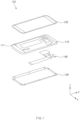
- FIG. 1 is an exploded perspective view of an electronic device 101 according to various embodiments.
- the electronic device 101 may be at least one of a portable communication device such as a smartphone, and a tablet, a computer device, a portable multimedia device, a portable medical device, a camera, a wearable device, or an artificial intelligence (AI) speaker.
- a portable communication device such as a smartphone, and a tablet
- a computer device such as a smartphone, and a tablet
- a portable multimedia device such as a smartphone, and a tablet
- a portable medical device such as a portable medical device
- a camera such as a wearable device
- AI artificial intelligence
- the electronic device 101 includes a side bezel structure 110, may include a support member 111, includes a front plate 120, a rear plate 130, and a printed circuit board (PCB) 140.
- the electronic device 101 further includes at least one component other than the components shown in FIG. 1 .
- the electronic device 101 further includes an antenna and may further include at least one of a display, a battery, an electromagnetic induction panel, a memory, an interface (e.g., HDMI (high definition multimedia interface), an USB (universal serial bus) interface, a SD card interface, and/or an audio interface), or a rear case.
- HDMI high definition multimedia interface
- USB universal serial bus
- the front plate 120 is configured to face a first surface of the electronic device 101 (e.g., in +z axis direction).
- the rear plate 130 is configured to face a second surface opposite to the first surface (e.g., in -z axis direction).
- the side bezel structure 110 may be referred to as a frame or a case.
- the side bezel structure 110 is connected to the front plate 120 and the rear plate 130, and to surround sides of the electronic device 101.
- the side bezel structure 110 may be made of a metal material.
- the side bezel structure 110 and a ground area of the printed circuit board 140 may be electrically separated from each other to prevent risk of electric shock to the user.
- an area of the side bezel structure 110 may be larger than an area of the printed circuit board 140.
- the side bezel structure 10 may be combined with the printed circuit board 140 while the side bezel structure 110 is spaced from the printed circuit board 140.
- the support member 111 (e.g., a bracket) may be disposed inside the electronic device 101 and may be connected to the side bezel structure 110, or may be integrally formed with the side bezel structure 110.
- the support member 111 may be made of, for example, a metallic material and/or a non-metal (e.g., a polymer material).
- the support member 111 may be coupled, on one surface thereof (e.g., in +z axis), to a display, and may be coupled, on the other surface thereof (e.g., in -z axis), to the printed circuit board 140.
- the electronic device 101 may be free of the support member 111.
- the printed circuit board 140 may include components for implementing functions of the electronic device 101.
- the printed circuit board 140 may include at least one of a processor, a memory, or an interface.
- the processor may be, for example, at least one of a central processing unit, an application processor, a graphics processing unit, an image signal processor, a sensor hub processor, or a communication processor.
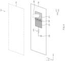
- FIG. 2 illustrates a structure of the printed circuit board 140 including a gap 240 defined between conductive pads.
- the printed circuit board 140 may include a conductive pad 210 configured to couple the side bezel structure 110 and the printed circuit board 140 to each other in a partial area thereof, and a ground area 230 that is electrically connected to the conductive pad 210 in another partial area thereof.
- the printed circuit board 140 may further include a separate connector 220 in order to more easily couple the printed circuit board 140 and the side bezel structure 110 to each other.
- the conductive pad 210 may be divided into a first conductive pad 211 and a second conductive pad 212.
- the first conductive pad 211 may be coupled to the side bezel structure 110
- the second conductive pad 212 may be electrically separated from the first conductive pad 211 but may be electrically connected to the ground area 230.
- the first conductive pad 211 and the second conductive pad 212 may be spaced from each other by the gap 240 across which a current having a voltage equal to or higher than a threshold voltage may flow.
- the gap 240 defined between the first conductive pad 211 and the second conductive pad 212 may be referred to as a narrow gap or a spark gap.
- the insulation function by the gap 240 may be limited.
- the current having the voltage higher than the threshold voltage may be transmitted to the ground area 230 through the first conductive pad 211 and the second conductive pad 212.
- the threshold voltage may be low.
- FIG. 3 illustrates shapes of one side of the first conductive pad 211 and one side of the second conductive pad 212 according to various embodiments.
- one side of the first conductive pad 211 and one side of the second conductive pad 212 may be spaced from each other by a gap 240 extending in a zig-zag manner.
- the current may be transmitted more efficiently between the first conductive pad 211 and the second conductive pad 212 through the gap 240 extending in the zig-zag manner because the zig-zag manner allows a length along which one side of the first conductive pad 211 and one side of the second conductive pad 212 face away each other to increase, and allows a spacing between the first conductive pad 211 and the second conductive pad 212 to decrease.
- one side of the first conductive pad 211 and one side of the second conductive pad 212 may be spaced from each other by the gap 240 extending in a right-angled zig-zag manner 310.
- one side of the first conductive pad 211 and one side of the second conductive pad 212 may be spaced from each other by the gap 240 in a non-right angled zig-zag manner 320.
- one side of the first conductive pad 211 and one side of the second conductive pad 212 may be spaced from each other by the gap 240 in a round zig-zag manner 330.
- one side of the first conductive pad 211 and one side of the second conductive pad 212 may be spaced from each other by the gap extending in various zig-zag manners in addition to those shown in FIG. 3 .
- the gap 240 defined between one side of the first conductive pad 211 and one side of the second conductive pad 212 may not extend in the zig-zag manner.
- a portion protruding from one side of the first conductive pad 211 e.g., a portion 311 of the reference number 301
- a portion protruding from one side of the second conductive pad 212 may face away a portion protruding from one side of the second conductive pad 212 (e.g., a portion 312 of the reference number 301).
- FIG. 4 shows a structure of the printed circuit board 140 further including a resistor element 410.
- the printed circuit board 140 may further include the resistor element 410 disposed between the second conductive pad 212 and the ground area 230.
- the resistor element 410 may be, for example, a SMT (surface mount technology) resistor element (or a resistor element mounted using SMT).
- SMT surface mount technology
- secondary noise or electromagnetic field which causes malfunction of components of the electronic device 101 (or components mounted on the PCB 140) may occur.
- the resistor element 410 disposed between the second conductive pad 212 and the ground area 230 may reduce a magnitude of the voltage to prevent the secondary noise.
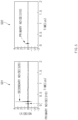
- FIG. 5 is a graph 502 illustrating a change amount of a voltage generated on the printed circuit board 140 over time.
- a graph 501 may represent a voltage of a noise signal over time when a surge voltage is applied from the side bezel structure 110 when an existing ESD protection element is mounted on the printed circuit board 140.
- the graph 502 may represent a voltage of a noise signal over time when the surge voltage is applied from the side bezel structure 110 while the first conductive pad 211 and the second conductive pad 212 on the printed circuit board 140 are separated from each other, and the resistor element 410 is disposed between the second conductive pad 212 and the ground area 230.
- secondary noise 520 generated due to a high voltage in addition to primary noise 510 may be measured in the printed circuit board 140.
- the generated secondary noise 520 may cause malfunction of components included in the printed circuit board 140.
- the voltage decreases due to the resistor element 410, such that the secondary noise 520 may not be measured.
- FIG. 6 illustrates a structure of the printed circuit board 140 further including a capacitor 610.
- FIG. 6 shows an arrangement in which the capacitor 610 is further included in the structure of the printed circuit board 140 shown in FIG. 4 .
- the same principle may be applied to the structure of the printed circuit board 140 shown in FIG. 2 .
- FIG. 6 shows an example in which the gap 240 defined between the first conductive pad 211 and the second conductive pad 212 has the form shown in the reference numeral 302 in FIG. 3 .
- the same principle may be applied to other forms as shown in FIG. 3 .
- the printed circuit board 140 may further include the capacitor 610 between the connector 220 and the ground area 230.
- the capacitor 610 may be arranged in parallel with a series of the first conductive pad 211 and the second conductive pad 212.
- the capacitor 610 may adjust transmission/reception performance of a signal transmitted from the printed circuit board 140 to the side bezel structure 110 or vice versa through the connector 220 by using resonance.
- FIG. 7 shows a structure of the printed circuit board 140 including the capacitor 610 and the gap 240 defined between an antenna housing 720 and a communication circuit 710 according to various embodiments.
- FIG. 7 shows an embodiment in which the communication circuit 710 and the capacitor 610 are further included in the structure of the printed circuit board 140 shown in FIG. 4 .
- the same principle may be applied to the structure of the printed circuit board 140 shown in FIG. 2 .
- FIG. 7 shows an embodiment in which the gap 240 defined between the first conductive pad 211 and the second conductive pad 212 has the form shown in the reference numeral 302 of FIG. 3 .
- the same principle may be applied to other forms as shown in FIG. 3 .
- the printed circuit board 140 may be electrically connected to the antenna housing 720.
- the antenna housing 720 is configured to define at least a partial area of the side bezel structure 110 and perform an antenna function.
- the printed circuit board 140 includes the communication circuit 710 configured to process a signal in order to perform communication in a radio frequency band.
- the communication circuit 710 may correspond to a communication module 890 in FIG. 8 .
- the printed circuit board 140 further includes the capacitor 610 between the antenna housing 720 and the communication circuit 710.
- the capacitor 610 is arranged in parallel with a series of the first conductive pad 211 and the second conductive pad 212. While a frequency of signal transmissions may decrease due to the gap 240 defined between the first conductive pad 211 and the second conductive pad 212, the capacitor 610 may have a capacitance to increase signal transmission performance.
- FIG. 8 is a block diagram of an electronic device in a network environment according to various embodiments.
- an electronic device 101 may communicate with an electronic device 802 through a first network 898 (e.g., a short-range wireless communication) or may communicate with an electronic device 804 or a server 808 through a second network 899 (e.g., a long-distance wireless communication) in a network environment 800.
- the electronic device 101 may communicate with the electronic device 804 through the server 808.
- the electronic device 101 includes an antenna module 896 and may include a processor 820, a memory 830, an input device 850, a sound output device 855, a display device 860, an audio module 870, a sensor module 876, an interface 877, a haptic module 879, a camera module 880, a power management module 888, a battery 889, a communication module 890, a subscriber identification module 896.
- a processor 820 may include a processor 820, a memory 830, an input device 850, a sound output device 855, a display device 860, an audio module 870, a sensor module 876, an interface 877, a haptic module 879, a camera module 880, a power management module 888, a battery 889, a communication module 890, a subscriber identification module 896.
- at least one e.g., the display device 860 or the camera module 880
- components of the electronic device 101 may be omitted or other components
- some components may be integrated and implemented as in the case of the sensor module 876 (e.g., a fingerprint sensor, an iris sensor, or an illuminance sensor) embedded in the display device 860 (e.g., a display).
- the sensor module 876 e.g., a fingerprint sensor, an iris sensor, or an illuminance sensor
- the display device 860 e.g., a display
- the processor 820 may operate, for example, software (e.g., a program 840) to control at least one of other components (e.g., a hardware or software component) of the electronic device 101 connected to the processor 820 and may process and compute a variety of data.
- the processor 820 may load a command set or data, which is received from other components (e.g., the sensor module 876 or the communication module 890), into a volatile memory 832, may process the loaded command or data, and may store result data into a nonvolatile memory 834.
- the processor 820 may include a main processor 821 (e.g., a central processing unit or an application processor) and an auxiliary processor 823 (e.g., a graphic processing device, an image signal processor, a sensor hub processor, or a communication processor), which operates independently from the main processor 821, additionally or alternatively uses less power than the main processor 821, or is specified to a designated function.
- the auxiliary processor 823 may operate separately from the main processor 821 or embedded.
- the auxiliary processor 823 may control, for example, at least some of functions or states associated with at least one component (e.g., the display device 860, the sensor module 876, or the communication module 890) among the components of the electronic device 101 instead of the main processor 821 while the main processor 821 is in an inactive (e.g., sleep) state or together with the main processor 821 while the main processor 821 is in an active (e.g., an application execution) state.
- the auxiliary processor 823 e.g., the image signal processor or the communication processor
- the auxiliary processor 823 may be implemented as a part of another component (e.g., the camera module 880 or the communication module 890) that is functionally related to the auxiliary processor 823.
- the memory 830 may store a variety of data used by at least one component (e.g., the processor 820 or the sensor module 876) of the electronic device 101, for example, software (e.g., the program 840) and input data or output data with respect to commands associated with the software.
- the memory 830 may include the volatile memory 832 or the nonvolatile memory 834.
- the program 840 may be stored in the memory 830 as software and may include, for example, an operating system 842, a middleware 844, or an application 846.
- the input device 850 may be a device for receiving a command or data, which is used for a component (e.g., the processor 820) of the electronic device 101, from an outside (e.g., a user) of the electronic device 101 and may include, for example, a microphone, a mouse, or a keyboard.
- a component e.g., the processor 820
- the input device 850 may include, for example, a microphone, a mouse, or a keyboard.
- the sound output device 855 may be a device for outputting a sound signal to the outside of the electronic device 101 and may include, for example, a speaker used for general purposes, such as multimedia play or recordings play, and a receiver used only for receiving calls. According to an embodiment, the receiver and the speaker may be either integrally or separately implemented.
- the display device 860 may be a device for visually presenting information to the user of the electronic device 101 and may include, for example, a display, a hologram device, or a projector and a control circuit for controlling a corresponding device. According to an embodiment, the display device 860 may include a touch circuitry or a pressure sensor for measuring an intensity of pressure on the touch.
- the audio module 870 may convert a sound and an electrical signal in dual directions. According to an embodiment, the audio module 870 may obtain the sound through the input device 850 or may output the sound through an external electronic device (e.g., the electronic device 802 (e.g., a speaker or a headphone)) wired or wirelessly connected to the sound output device 855 or the electronic device 101.
- an external electronic device e.g., the electronic device 802 (e.g., a speaker or a headphone)
- the sensor module 876 may generate an electrical signal or a data value corresponding to an operating state (e.g., power or temperature) inside or an environmental state outside the electronic device 101.
- the sensor module 876 may include, for example, a gesture sensor, a gyro sensor, a barometric pressure sensor, a magnetic sensor, an acceleration sensor, a grip sensor, a proximity sensor, a color sensor, an infrared sensor, a biometric sensor, a temperature sensor, a humidity sensor, or an illuminance sensor.
- the interface 877 may support a designated protocol wired or wirelessly connected to the external electronic device (e.g., the electronic device 802).
- the interface 877 may include, for example, an HDMI (high-definition multimedia interface), a USB (universal serial bus) interface, an SD card interface, or an audio interface.
- a connecting terminal 878 may include a connector that physically connects the electronic device 101 to the external electronic device (e.g., the electronic device 802), for example, an HDMI connector, a USB connector, an SD card connector, or an audio connector (e.g., a headphone connector).
- the haptic module 879 may convert an electrical signal to a mechanical stimulation (e.g., vibration or movement) or an electrical stimulation perceived by the user through tactile or kinesthetic sensations.
- the haptic module 879 may include, for example, a motor, a piezoelectric element, or an electric stimulator.
- the camera module 880 may shoot a still image or a video image.
- the camera module 880 may include, for example, at least one lens, an image sensor, an image signal processor, or a flash.
- the power management module 888 may be a module for managing power supplied to the electronic device 101 and may serve as at least a part of a power management integrated circuit (PMIC).
- PMIC power management integrated circuit
- the battery 889 may be a device for supplying power to at least one component of the electronic device 101 and may include, for example, a nonrechargeable (primary) battery, a rechargeable (secondary) battery, or a fuel cell.
- the communication module 890 may establish a wired or wireless communication channel between the electronic device 101 and the external electronic device (e.g., the electronic device 802, the electronic device 804, or the server 808) and support communication execution through the established communication channel.
- the communication module 890 may include at least one communication processor operating independently from the processor 820 (e.g., the application processor) and supporting the wired communication or the wireless communication.
- the communication module 890 may include a wireless communication module 892 (e.g., a cellular communication module, a short-range wireless communication module, or a GNSS (global navigation satellite system) communication module) or a wired communication module 894 (e.g., an LAN (local area network) communication module or a power line communication module) and may communicate with the external electronic device using a corresponding communication module among them through the first network 898 (e.g., the short-range communication network such as a Bluetooth, a WiFi direct, or an IrDA (infrared data association)) or the second network 899 (e.g., the long-distance wireless communication network such as a cellular network, an internet, or a computer network (e.g., LAN or WAN)).
- the above-mentioned various communication modules 890 may be implemented into one chip or into separate chips, respectively.
- the wireless communication module 892 may identify and authenticate the electronic device 101 using user information stored in the subscriber identification module 896 in the communication network.
- the antenna module 897 may include one or more antennas to transmit or receive the signal or power to or from an external source.
- the communication module 890 e.g., the wireless communication module 892
- Some components among the components may be connected to each other through a communication method (e.g., a bus, a GPIO (general purpose input/output), an SPI (serial peripheral interface), or an MIPI (mobile industry processor interface)) used between peripheral devices to exchange signals (e.g., a command or data) with each other.
- a communication method e.g., a bus, a GPIO (general purpose input/output), an SPI (serial peripheral interface), or an MIPI (mobile industry processor interface) used between peripheral devices to exchange signals (e.g., a command or data) with each other.
- the command or data may be transmitted or received between the electronic device 101 and the external electronic device 804 through the server 808 connected to the second network 899.
- Each of the electronic devices 802 and 804 may be the same or different types as or from the electronic device 101.
- all or some of the operations performed by the electronic device 101 may be performed by another electronic device or a plurality of external electronic devices.
- the electronic device 101 may request the external electronic device to perform at least some of the functions related to the functions or services, in addition to or instead of performing the functions or services by itself.
- the external electronic device receiving the request may carry out the requested function or the additional function and transmit the result to the electronic device 101.
- the electronic device 101 may provide the requested functions or services based on the received result as is or after additionally processing the received result.
- a cloud computing, distributed computing, or client-server computing technology may be used.
- the electronic device (e.g., the electronic device 101 in FIG. 1 ) includes a first plate (e.g., the front plate 120 in FIG. 1 ) configured to define one surface of the electronic device, a second plate (e.g. the rear plate 130 in FIG. 1 ) configured to be opposite to the first plate, a side bezel structure (e.g., the side bezel structure 110 in FIG. 1 ) configured to be connected to the first plate and the second plate and to surround a side of the electronic device, and a printed circuit board (e.g., the printed circuit board 140 in FIG.
- a first plate e.g., the front plate 120 in FIG. 1
- a second plate e.g. the rear plate 130 in FIG. 1
- a side bezel structure e.g., the side bezel structure 110 in FIG. 1
- a printed circuit board e.g., the printed circuit board 140 in FIG.
- the printed circuit board includes a ground area (e.g., the ground area 230 in FIG. 2 ), a first conductive pad (e.g., the first conductive pad 211 in FIG. 2 ) disposed in one area of the printed circuit board and configured to allow coupling between the side bezel structure and the printed circuit board, and a second conductive pad area (e.g., the second conductive pad 212 in FIG. 2 ) electrically connected to the ground area and disposed between the first conductive pad and the ground, wherein the first conductive pad and the second conductive pad may be spaced from each other by a gap (e.g., the gap 240 in FIG. 2 ) through which a current having a voltage equal to or higher than a threshold voltage may flow between the first conductive pad and the second conductive pad.
- a gap e.g., the gap 240 in FIG. 2
- the side bezel structure may be made of a metal material.
- the electronic device may further include a connector (e.g., the connector 220 in FIG. 2 ) operatively coupled to the first conductive pad and configured to facilitate coupling between the first conductive pad and the side bezel structure.
- a connector e.g., the connector 220 in FIG. 2
- each of one side of the first conductive pad and one side of the second conductive pad facing away the one side of the first conductive pad may extend in a zig-zag manner.
- the zig-zag manner may include a right-angled zig-zag manner, a non-right-angled zig-zag manner or a round zig-zag manner
- the electronic device further includes a resistor element (e.g., the resistor element 410 of FIG. 4 ) disposed between the second conductive pad and the ground area.
- a resistor element e.g., the resistor element 410 of FIG. 4
- the resistor element may include a SMT resistor element.
- the side bezel structure may be connected to a top of the printed circuit board and may have a larger area than an area of the printed circuit board.
- the side bezel structure may be coupled to the printed circuit board while an inner side surface of the side bezel structure is spaced from a side surface of the PCB.
- the printed circuit board may be configured to include an application processor (AP) of the electronic device.
- AP application processor
- the electronic device (e.g., the electronic device 101 in FIG. 1 ) includes a first plate (e.g., the front plate 120 in FIG. 1 ) configured to define one surface of the electronic device, a second plate (e.g. the rear plate 130 in FIG. 1 ) configured to be opposite to the first plate, a side bezel structure (e.g., the side bezel structure 110 in FIG. 1 ) configured to be connected to the first plate and the second plate and to surround a side of the electronic device, and a printed circuit board (e.g., the printed circuit board 140 in FIG.
- a first plate e.g., the front plate 120 in FIG. 1
- a second plate e.g. the rear plate 130 in FIG. 1
- a side bezel structure e.g., the side bezel structure 110 in FIG. 1
- a printed circuit board e.g., the printed circuit board 140 in FIG.
- the printed circuit board includes a ground area (e.g., the ground area 230 in FIG. 2 ), a first conductive pad (e.g., the first conductive pad 211 in FIG. 2 ) disposed in one area of the printed circuit board and configured to allow coupling between the side bezel structure and the printed circuit board, and a second conductive pad area (e.g., the second conductive pad 212 in FIG.
- a ground area e.g., the ground area 230 in FIG. 2
- a first conductive pad e.g., the first conductive pad 211 in FIG. 2
- a second conductive pad area e.g., the second conductive pad 212 in FIG.
- first conductive pad and the second conductive pad may be spaced from each other by a gap (e.g., the gap 240 in FIG. 2 ) through which a current having a voltage equal to or higher than a threshold voltage may flow between the first conductive pad and the second conductive pad.
- a gap e.g., the gap 240 in FIG. 2
- the side bezel structure may be made of a metal material.
- the electronic device may further include a connector (e.g., the connector 220 in FIG. 2 ) operatively coupled to the first conductive pad and configured to facilitate coupling between the first conductive pad and the side bezel structure.
- a connector e.g., the connector 220 in FIG. 2
- each of one side of the first conductive pad and one side of the second conductive pad facing away the one side of the first conductive pad may extend in a zig-zag manner.
- the zig-zag manner may include a right-angled zig-zag manner, a non-right-angled zig-zag manner or a round zig-zag manner
- the electronic device further includes a resistor element (e.g., the resistor element 410 of FIG. 4 ) disposed between the second conductive pad and the ground area.
- a resistor element e.g., the resistor element 410 of FIG. 4
- the resistor element may include a SMT resistor element.
- the side bezel structure may be connected to a top of the printed circuit board and may have a larger area than an area of the printed circuit board.
- the side bezel structure may be coupled to the printed circuit board wile an inner side surface of the side bezel structure is spaced from a side surface of the PCB.
- the printed circuit board may be configured to include an AP of the electronic device.
- the electronic device may be various types of devices.
- the electronic device may include, for example, at least one of a portable communication device (e.g., a smartphone), a computer device, a portable multimedia device, a mobile medical appliance, a camera, a wearable device, or a home appliance.
- a portable communication device e.g., a smartphone
- a computer device e.g
- a first”, “a second”, “the first”, or “the second”, used in herein may refer to various components regardless of the order and/or the importance, but do not limit the corresponding components.
- the above expressions are used merely for the purpose of distinguishing a component from the other components. It should be understood that when a component (e.g., a first component) is referred to as being (operatively or communicatively) "connected,” or “coupled,” to another component (e.g., a second component), it may be directly connected or coupled directly to the other component or any other component (e.g., a third component) may be interposed between them.
- module used herein may represent, for example, a unit including one or more combinations of hardware, software and firmware.
- module may be interchangeably used with the terms “logic”, “logical block”, “part” and “circuit”.
- the “module” may be a minimum unit of an integrated part or may be a part thereof.
- the “module” may be a minimum unit for performing one or more functions or a part thereof.
- the “module” may include an application-specific integrated circuit (ASIC).
- ASIC application-specific integrated circuit
- Various embodiments of the disclosure may be implemented by software (e.g., the program 840) including an instruction stored in a machine-readable storage media (e.g., an internal memory 836 or an external memory 838) readable by a machine (e.g., a computer).
- the machine may be a device that calls the instruction from the machine-readable storage media and operates depending on the called instruction and may include the electronic device (e.g., the electronic device 101).
- the processor e.g., the processor 820
- the processor may perform a function corresponding to the instruction directly or using other components under the control of the processor.
- the instruction may include a code generated or executed by a compiler or an interpreter.
- the machine-readable storage media may be provided in the form of non-transitory storage media.
- non-transitory is a limitation of the medium itself (i.e., tangible, not a signal) as opposed to a limitation on data storage persistency.
- a method may be provided as a part of a computer program product.
- the computer program product may be traded between a seller and a buyer as a product.
- the computer program product may be distributed in the form of machine-readable storage medium (e.g., a compact disc read only memory (CD-ROM)) or may be distributed only through an application store (e.g., a Play Store TM ).
- an application store e.g., a Play Store TM
- at least a portion of the computer program product may be temporarily stored or generated in a storage medium such as a memory of a manufacturer's server, an application store's server, or a relay server.
- Each component may include at least one of the above components, and a portion of the above sub-components may be omitted, or additional other sub-components may be further included.
- some components e.g., the module or the program
- Operations performed by a module, a programming, or other components according to various embodiments of the disclosure may be executed sequentially, in parallel, repeatedly, or in a heuristic method. Also, at least some operations may be executed in different sequences, omitted, or other operations may be added.
Landscapes
- Engineering & Computer Science (AREA)
- Signal Processing (AREA)
- Microelectronics & Electronic Packaging (AREA)
- Telephone Set Structure (AREA)
- Casings For Electric Apparatus (AREA)
Description
- Embodiments disclosed in the disclosure relate to an electronic device for protecting components from a surge voltage, and a structure thereof.
- A surge voltage may mean a voltage that rapidly increases during a short time. The surge voltage may be caused by sudden load change in an adjacent circuit, power instability, interference via coupled wires, switch operation, lightning strikes, or ESD (electro static discharge). Because the surge voltage may cause malfunction of components included inside the electronic device, the electronic device must satisfy a test standard (e.g. IEC-61000-4-2 or IEC-61000-4-5) specified by IEC (international electrotechnical commission).
- The electronic device may include a frame made of a metal material as at least one surface surrounding the electronic device. Because the frame made of the metal material may transmit current, this may cause a risk of electric shock to a user. For example, when the user charges the electronic device using an unstable power system or a bad quality charger, current is generated in a printed circuit board (PCB) included in the electronic device. Thus, when the user touches the frame, the current may be delivered to the user through the frame. In order to protect the user from the risk of electric shock, the frame and a ground area or a ground (GND) of the printed circuit board may be spaced apart from each other.
EP1612897 ,EP1986297 ,US2017/048954 ,US2018/103531 ,KR20170065386 KR20150026569 KR100541501 KR20180049945 KR20170101144 - When the ground area of the printed circuit board is spaced apart from the frame made of the metal, a potential difference between the frame and the printed circuit board may rise up when a high voltage such as surge voltage is generated outside the electronic device. When the increased potential difference satisfies a specified condition (e.g., air gap breakdown condition), ESD current may flow from the frame to the printed circuit board. To protect the printed circuit board from the surge voltage, an ESD protection element may be disposed between the frame and the ground area of the printed circuit board. However, the ESD protection element does not reduce secondary noise due to the surge voltage and is expensive. This may lead to an increase in a production cost of the electronic device.
- Various embodiments disclosed in the disclosure are intended to provide an electronic device for protecting components of the electronic device from the surge voltage, and a structure thereof.
- An electronic device according to the invention is defined by
claim 1. - According to the embodiments disclosed in the disclosure, the electronic device may protect the components from the surge voltage applied from an outside of the electronic device, and at the same time, may reduce the current flowing in the frame made of the metal material and in the printed circuit board to prevent the risk of electric shock toward the user.
- According to the embodiments disclosed in the disclosure, the electronic device may achieve cost reduction via a structural feature that replaces the ESD protection element.
- In addition to the above effects, various effects that are directly or indirectly recognized based on the disclosure may be provided.
-
Figures 1 to 5 show examples, useful for understanding the invention. -
FIG. 1 is an exploded perspective view of an electronic device according to various embodiments. -
FIG. 2 shows a structure of a printed circuit board (PCB) including a gap defined between conductive pads. -
FIG. 3 is a diagram illustrating shapes of one side of a first conductive pad and one side of a second conductive pad according to various embodiments. -
FIG. 4 shows a structure of a printed circuit board further including a resistor element. -
FIG. 5 is a graph illustrating a change amount of a voltage generated on a printed circuit board over time. -
FIG. 6 illustrates a structure of a printed circuit board further including a capacitor according to the invention. -
FIG. 7 shows a structure of a printed circuit board including a capacitor and a gap defined between an antenna housing and a communication circuit according to according to the invention. -
FIG. 8 is a block diagram of an electronic device in a network environment according to various embodiments. - With respect to the description of the drawings, the same or similar reference numerals may refer to the same or similar components.
- Hereinafter, various embodiments of the disclosure will be described with reference to the accompanying drawings. However, the embodiments are not intended to limit the disclosure thereto. Rather, it should be understood that various modifications of, equivalents to, and/or alternatives to the embodiments of the disclosure may be made within the scope of the invention as defined by the claims.
-
FIG. 1 is an exploded perspective view of anelectronic device 101 according to various embodiments. - Referring to
FIG. 1 , theelectronic device 101 may be at least one of a portable communication device such as a smartphone, and a tablet, a computer device, a portable multimedia device, a portable medical device, a camera, a wearable device, or an artificial intelligence (AI) speaker. - According to an embodiment, the
electronic device 101 includes aside bezel structure 110, may include asupport member 111, includes afront plate 120, arear plate 130, and a printed circuit board (PCB) 140. According to an embodiment, theelectronic device 101 further includes at least one component other than the components shown inFIG. 1 . For example, theelectronic device 101 further includes an antenna and may further include at least one of a display, a battery, an electromagnetic induction panel, a memory, an interface (e.g., HDMI (high definition multimedia interface), an USB (universal serial bus) interface, a SD card interface, and/or an audio interface), or a rear case.. - According to one embodiment, the
front plate 120 is configured to face a first surface of the electronic device 101 (e.g., in +z axis direction). Therear plate 130 is configured to face a second surface opposite to the first surface (e.g., in -z axis direction). - According to an embodiment, the
side bezel structure 110 may be referred to as a frame or a case. Theside bezel structure 110 is connected to thefront plate 120 and therear plate 130, and to surround sides of theelectronic device 101. According to an embodiment, theside bezel structure 110 may be made of a metal material. When theside bezel structure 110 is made of the metal material, theside bezel structure 110 and a ground area of the printedcircuit board 140 may be electrically separated from each other to prevent risk of electric shock to the user. For example, an area of theside bezel structure 110 may be larger than an area of the printedcircuit board 140. The side bezel structure 10 may be combined with the printedcircuit board 140 while theside bezel structure 110 is spaced from the printedcircuit board 140. - According to an embodiment, the support member 111 (e.g., a bracket) may be disposed inside the
electronic device 101 and may be connected to theside bezel structure 110, or may be integrally formed with theside bezel structure 110. Thesupport member 111 may be made of, for example, a metallic material and/or a non-metal (e.g., a polymer material). Thesupport member 111 may be coupled, on one surface thereof (e.g., in +z axis), to a display, and may be coupled, on the other surface thereof (e.g., in -z axis), to the printedcircuit board 140. According to an embodiment, theelectronic device 101 may be free of thesupport member 111. - According to an embodiment, the printed
circuit board 140 may include components for implementing functions of theelectronic device 101. For example, the printedcircuit board 140 may include at least one of a processor, a memory, or an interface. The processor may be, for example, at least one of a central processing unit, an application processor, a graphics processing unit, an image signal processor, a sensor hub processor, or a communication processor. -
FIG. 2 illustrates a structure of the printedcircuit board 140 including agap 240 defined between conductive pads. - Referring to
FIG. 2 , theprinted circuit board 140 may include a conductive pad 210 configured to couple theside bezel structure 110 and the printedcircuit board 140 to each other in a partial area thereof, and aground area 230 that is electrically connected to the conductive pad 210 in another partial area thereof. The printedcircuit board 140 may further include aseparate connector 220 in order to more easily couple the printedcircuit board 140 and theside bezel structure 110 to each other. - In order to prevent the risk of electric shock to the user by prevent current from transmitting from the printed
circuit board 140 to theside bezel structure 110, the conductive pad 210 may be divided into a firstconductive pad 211 and a secondconductive pad 212. In other words, the firstconductive pad 211 may be coupled to theside bezel structure 110, and the secondconductive pad 212 may be electrically separated from the firstconductive pad 211 but may be electrically connected to theground area 230. - The first
conductive pad 211 and the secondconductive pad 212 may be spaced from each other by thegap 240 across which a current having a voltage equal to or higher than a threshold voltage may flow. Thegap 240 defined between the firstconductive pad 211 and the secondconductive pad 212 may be referred to as a narrow gap or a spark gap. - Due to the
gap 240 defined between the firstconductive pad 211 and the secondconductive pad 212, current having a voltage lower than the threshold voltage cannot be transferred from the printedcircuit board 140 to theside bezel structure 110 even when the current having the voltage lower than the threshold voltage occurs in the printedcircuit board 140. Because the current generated in the printedcircuit board 140 is not transferred to theside bezel structure 110, the risk of electric shock to the user may be prevented. - When current having a voltage (e.g., surge voltage) higher than the threshold voltage occurs in the
side bezel structure 110, the insulation function by thegap 240 may be limited. Thus, the current having the voltage higher than the threshold voltage may be transmitted to theground area 230 through the firstconductive pad 211 and the secondconductive pad 212. When the current having the voltage higher than the threshold voltage is transmitted to theground area 230 through the firstconductive pad 211 and the secondconductive pad 212, malfunction of components included in the electronic device 101 (or components included in the printed circuit board 140) may be prevented. As thegap 240 is narrower, the threshold voltage may be low. -
FIG. 3 illustrates shapes of one side of the firstconductive pad 211 and one side of the secondconductive pad 212 according to various embodiments. - Referring to
FIG. 3 , one side of the firstconductive pad 211 and one side of the secondconductive pad 212 may be spaced from each other by agap 240 extending in a zig-zag manner. The current may be transmitted more efficiently between the firstconductive pad 211 and the secondconductive pad 212 through thegap 240 extending in the zig-zag manner because the zig-zag manner allows a length along which one side of the firstconductive pad 211 and one side of the secondconductive pad 212 face away each other to increase, and allows a spacing between the firstconductive pad 211 and the secondconductive pad 212 to decrease. - In one example, as shown in a
reference number 301, one side of the firstconductive pad 211 and one side of the secondconductive pad 212 may be spaced from each other by thegap 240 extending in a right-angled zig-zag manner 310. In another example, as shown by areference numeral 302, one side of the firstconductive pad 211 and one side of the secondconductive pad 212 may be spaced from each other by thegap 240 in a non-right angled zig-zag manner 320. In another example, as shown by areference numeral 303, one side of the firstconductive pad 211 and one side of the secondconductive pad 212 may be spaced from each other by thegap 240 in a round zig-zag manner 330. According to an embodiment, one side of the firstconductive pad 211 and one side of the secondconductive pad 212 may be spaced from each other by the gap extending in various zig-zag manners in addition to those shown inFIG. 3 . - According to an embodiment, the
gap 240 defined between one side of the firstconductive pad 211 and one side of the secondconductive pad 212 may not extend in the zig-zag manner. For example, as shown in areference number 304, a portion protruding from one side of the first conductive pad 211 (e.g., aportion 311 of the reference number 301) may face away a portion protruding from one side of the second conductive pad 212 (e.g., aportion 312 of the reference number 301). -
FIG. 4 shows a structure of the printedcircuit board 140 further including aresistor element 410. - Referring to
FIG. 4 , the printedcircuit board 140 may further include theresistor element 410 disposed between the secondconductive pad 212 and theground area 230. Theresistor element 410 may be, for example, a SMT (surface mount technology) resistor element (or a resistor element mounted using SMT). When current having a voltage (e.g., a surge voltage) higher than the threshold voltage flows to theground area 230 through the firstconductive pad 211 and the secondconductive pad 212, secondary noise (or electromagnetic field) which causes malfunction of components of the electronic device 101 (or components mounted on the PCB 140) may occur. Theresistor element 410 disposed between the secondconductive pad 212 and theground area 230 may reduce a magnitude of the voltage to prevent the secondary noise. -
FIG. 5 is agraph 502 illustrating a change amount of a voltage generated on the printedcircuit board 140 over time. - Referring to
FIG. 5 , agraph 501 may represent a voltage of a noise signal over time when a surge voltage is applied from theside bezel structure 110 when an existing ESD protection element is mounted on the printedcircuit board 140. Thegraph 502 may represent a voltage of a noise signal over time when the surge voltage is applied from theside bezel structure 110 while the firstconductive pad 211 and the secondconductive pad 212 on the printedcircuit board 140 are separated from each other, and theresistor element 410 is disposed between the secondconductive pad 212 and theground area 230. - Referring to the
graph 501,secondary noise 520 generated due to a high voltage in addition toprimary noise 510 may be measured in the printedcircuit board 140. The generatedsecondary noise 520 may cause malfunction of components included in the printedcircuit board 140. Referring to thegraph 520, the voltage decreases due to theresistor element 410, such that thesecondary noise 520 may not be measured. -
FIG. 6 illustrates a structure of the printedcircuit board 140 further including acapacitor 610.FIG. 6 shows an arrangement in which thecapacitor 610 is further included in the structure of the printedcircuit board 140 shown inFIG. 4 . The same principle may be applied to the structure of the printedcircuit board 140 shown inFIG. 2 . Further,FIG. 6 shows an example in which thegap 240 defined between the firstconductive pad 211 and the secondconductive pad 212 has the form shown in thereference numeral 302 inFIG. 3 . However, the same principle may be applied to other forms as shown inFIG. 3 . - Referring to
FIG. 6 , the printedcircuit board 140 may further include thecapacitor 610 between theconnector 220 and theground area 230. For example, thecapacitor 610 may be arranged in parallel with a series of the firstconductive pad 211 and the secondconductive pad 212. - When the
side bezel structure 110 is made of the metal material, at least a partial area of theside bezel structure 110 performs an antenna function for transmitting a signal in a radio frequency band. Because thecapacitor 610 has a specified capacitance, thecapacitor 610 may adjust transmission/reception performance of a signal transmitted from the printedcircuit board 140 to theside bezel structure 110 or vice versa through theconnector 220 by using resonance. -
FIG. 7 shows a structure of the printedcircuit board 140 including thecapacitor 610 and thegap 240 defined between anantenna housing 720 and acommunication circuit 710 according to various embodiments.FIG. 7 shows an embodiment in which thecommunication circuit 710 and thecapacitor 610 are further included in the structure of the printedcircuit board 140 shown inFIG. 4 . However, the same principle may be applied to the structure of the printedcircuit board 140 shown inFIG. 2 . Further,FIG. 7 shows an embodiment in which thegap 240 defined between the firstconductive pad 211 and the secondconductive pad 212 has the form shown in thereference numeral 302 ofFIG. 3 . However, the same principle may be applied to other forms as shown inFIG. 3 . - Referring to
FIG. 7 , the printedcircuit board 140 may be electrically connected to theantenna housing 720. According to an embodiment, theantenna housing 720 is configured to define at least a partial area of theside bezel structure 110 and perform an antenna function. - According to an embodiment, the printed
circuit board 140 includes thecommunication circuit 710 configured to process a signal in order to perform communication in a radio frequency band. For example, thecommunication circuit 710 may correspond to acommunication module 890 inFIG. 8 . - According to an embodiment, the printed
circuit board 140 further includes thecapacitor 610 between theantenna housing 720 and thecommunication circuit 710. For example, thecapacitor 610 is arranged in parallel with a series of the firstconductive pad 211 and the secondconductive pad 212. While a frequency of signal transmissions may decrease due to thegap 240 defined between the firstconductive pad 211 and the secondconductive pad 212, thecapacitor 610 may have a capacitance to increase signal transmission performance. -
FIG. 8 is a block diagram of an electronic device in a network environment according to various embodiments. - Referring to
FIG. 8 , anelectronic device 101 may communicate with anelectronic device 802 through a first network 898 (e.g., a short-range wireless communication) or may communicate with anelectronic device 804 or aserver 808 through a second network 899 (e.g., a long-distance wireless communication) in anetwork environment 800. According to an embodiment, theelectronic device 101 may communicate with theelectronic device 804 through theserver 808. According to an embodiment, theelectronic device 101 includes anantenna module 896 and may include aprocessor 820, amemory 830, aninput device 850, asound output device 855, adisplay device 860, anaudio module 870, asensor module 876, aninterface 877, ahaptic module 879, acamera module 880, apower management module 888, abattery 889, acommunication module 890, asubscriber identification module 896. According to some embodiments, at least one (e.g., thedisplay device 860 or the camera module 880) among components of theelectronic device 101 may be omitted or other components may be added to theelectronic device 101. According to some embodiments, some components may be integrated and implemented as in the case of the sensor module 876 (e.g., a fingerprint sensor, an iris sensor, or an illuminance sensor) embedded in the display device 860 (e.g., a display). - The
processor 820 may operate, for example, software (e.g., a program 840) to control at least one of other components (e.g., a hardware or software component) of theelectronic device 101 connected to theprocessor 820 and may process and compute a variety of data. Theprocessor 820 may load a command set or data, which is received from other components (e.g., thesensor module 876 or the communication module 890), into avolatile memory 832, may process the loaded command or data, and may store result data into anonvolatile memory 834. According to an embodiment, theprocessor 820 may include a main processor 821 (e.g., a central processing unit or an application processor) and an auxiliary processor 823 (e.g., a graphic processing device, an image signal processor, a sensor hub processor, or a communication processor), which operates independently from themain processor 821, additionally or alternatively uses less power than themain processor 821, or is specified to a designated function. In this case, theauxiliary processor 823 may operate separately from themain processor 821 or embedded. - In this case, the
auxiliary processor 823 may control, for example, at least some of functions or states associated with at least one component (e.g., thedisplay device 860, thesensor module 876, or the communication module 890) among the components of theelectronic device 101 instead of themain processor 821 while themain processor 821 is in an inactive (e.g., sleep) state or together with themain processor 821 while themain processor 821 is in an active (e.g., an application execution) state. According to an embodiment, the auxiliary processor 823 (e.g., the image signal processor or the communication processor) may be implemented as a part of another component (e.g., thecamera module 880 or the communication module 890) that is functionally related to theauxiliary processor 823. Thememory 830 may store a variety of data used by at least one component (e.g., theprocessor 820 or the sensor module 876) of theelectronic device 101, for example, software (e.g., the program 840) and input data or output data with respect to commands associated with the software. Thememory 830 may include thevolatile memory 832 or thenonvolatile memory 834. - The
program 840 may be stored in thememory 830 as software and may include, for example, anoperating system 842, amiddleware 844, or anapplication 846. - The
input device 850 may be a device for receiving a command or data, which is used for a component (e.g., the processor 820) of theelectronic device 101, from an outside (e.g., a user) of theelectronic device 101 and may include, for example, a microphone, a mouse, or a keyboard. - The
sound output device 855 may be a device for outputting a sound signal to the outside of theelectronic device 101 and may include, for example, a speaker used for general purposes, such as multimedia play or recordings play, and a receiver used only for receiving calls. According to an embodiment, the receiver and the speaker may be either integrally or separately implemented. - The
display device 860 may be a device for visually presenting information to the user of theelectronic device 101 and may include, for example, a display, a hologram device, or a projector and a control circuit for controlling a corresponding device. According to an embodiment, thedisplay device 860 may include a touch circuitry or a pressure sensor for measuring an intensity of pressure on the touch. - The
audio module 870 may convert a sound and an electrical signal in dual directions. According to an embodiment, theaudio module 870 may obtain the sound through theinput device 850 or may output the sound through an external electronic device (e.g., the electronic device 802 (e.g., a speaker or a headphone)) wired or wirelessly connected to thesound output device 855 or theelectronic device 101. - The
sensor module 876 may generate an electrical signal or a data value corresponding to an operating state (e.g., power or temperature) inside or an environmental state outside theelectronic device 101. Thesensor module 876 may include, for example, a gesture sensor, a gyro sensor, a barometric pressure sensor, a magnetic sensor, an acceleration sensor, a grip sensor, a proximity sensor, a color sensor, an infrared sensor, a biometric sensor, a temperature sensor, a humidity sensor, or an illuminance sensor. - The
interface 877 may support a designated protocol wired or wirelessly connected to the external electronic device (e.g., the electronic device 802). According to an embodiment, theinterface 877 may include, for example, an HDMI (high-definition multimedia interface), a USB (universal serial bus) interface, an SD card interface, or an audio interface. - A connecting
terminal 878 may include a connector that physically connects theelectronic device 101 to the external electronic device (e.g., the electronic device 802), for example, an HDMI connector, a USB connector, an SD card connector, or an audio connector (e.g., a headphone connector). - The
haptic module 879 may convert an electrical signal to a mechanical stimulation (e.g., vibration or movement) or an electrical stimulation perceived by the user through tactile or kinesthetic sensations. Thehaptic module 879 may include, for example, a motor, a piezoelectric element, or an electric stimulator. - The
camera module 880 may shoot a still image or a video image. According to an embodiment, thecamera module 880 may include, for example, at least one lens, an image sensor, an image signal processor, or a flash. - The
power management module 888 may be a module for managing power supplied to theelectronic device 101 and may serve as at least a part of a power management integrated circuit (PMIC). - The
battery 889 may be a device for supplying power to at least one component of theelectronic device 101 and may include, for example, a nonrechargeable (primary) battery, a rechargeable (secondary) battery, or a fuel cell. - The
communication module 890 may establish a wired or wireless communication channel between theelectronic device 101 and the external electronic device (e.g., theelectronic device 802, theelectronic device 804, or the server 808) and support communication execution through the established communication channel. Thecommunication module 890 may include at least one communication processor operating independently from the processor 820 (e.g., the application processor) and supporting the wired communication or the wireless communication. According to an embodiment, thecommunication module 890 may include a wireless communication module 892 (e.g., a cellular communication module, a short-range wireless communication module, or a GNSS (global navigation satellite system) communication module) or a wired communication module 894 (e.g., an LAN (local area network) communication module or a power line communication module) and may communicate with the external electronic device using a corresponding communication module among them through the first network 898 (e.g., the short-range communication network such as a Bluetooth, a WiFi direct, or an IrDA (infrared data association)) or the second network 899 (e.g., the long-distance wireless communication network such as a cellular network, an internet, or a computer network (e.g., LAN or WAN)). The above-mentionedvarious communication modules 890 may be implemented into one chip or into separate chips, respectively. - According to an embodiment, the
wireless communication module 892 may identify and authenticate theelectronic device 101 using user information stored in thesubscriber identification module 896 in the communication network. - The
antenna module 897 may include one or more antennas to transmit or receive the signal or power to or from an external source. According to an embodiment, the communication module 890 (e.g., the wireless communication module 892) may transmit or receive the signal to or from the external electronic device through the antenna suitable for the communication method. - Some components among the components may be connected to each other through a communication method (e.g., a bus, a GPIO (general purpose input/output), an SPI (serial peripheral interface), or an MIPI (mobile industry processor interface)) used between peripheral devices to exchange signals (e.g., a command or data) with each other.
- According to an embodiment, the command or data may be transmitted or received between the
electronic device 101 and the externalelectronic device 804 through theserver 808 connected to thesecond network 899. Each of theelectronic devices electronic device 101. According to an embodiment, all or some of the operations performed by theelectronic device 101 may be performed by another electronic device or a plurality of external electronic devices. When theelectronic device 101 performs some functions or services automatically or by request, theelectronic device 101 may request the external electronic device to perform at least some of the functions related to the functions or services, in addition to or instead of performing the functions or services by itself. The external electronic device receiving the request may carry out the requested function or the additional function and transmit the result to theelectronic device 101. Theelectronic device 101 may provide the requested functions or services based on the received result as is or after additionally processing the received result. To this end, for example, a cloud computing, distributed computing, or client-server computing technology may be used. - As described above, the electronic device (e.g., the electronic device 101 in
FIG. 1 ) includes a first plate (e.g., the front plate 120 inFIG. 1 ) configured to define one surface of the electronic device, a second plate (e.g. the rear plate 130 inFIG. 1 ) configured to be opposite to the first plate, a side bezel structure (e.g., the side bezel structure 110 inFIG. 1 ) configured to be connected to the first plate and the second plate and to surround a side of the electronic device, and a printed circuit board (e.g., the printed circuit board 140 inFIG. 1 ) mounted inside the electronic device and configured to be connected to the side bezel structure, wherein the printed circuit board includes a ground area (e.g., the ground area 230 inFIG. 2 ), a first conductive pad (e.g., the first conductive pad 211 inFIG. 2 ) disposed in one area of the printed circuit board and configured to allow coupling between the side bezel structure and the printed circuit board, and a second conductive pad area (e.g., the second conductive pad 212 inFIG. 2 ) electrically connected to the ground area and disposed between the first conductive pad and the ground, wherein the first conductive pad and the second conductive pad may be spaced from each other by a gap (e.g., the gap 240 inFIG. 2 ) through which a current having a voltage equal to or higher than a threshold voltage may flow between the first conductive pad and the second conductive pad. - According to an embodiment, the side bezel structure may be made of a metal material.
- According to an embodiment, the electronic device may further include a connector (e.g., the
connector 220 inFIG. 2 ) operatively coupled to the first conductive pad and configured to facilitate coupling between the first conductive pad and the side bezel structure. - According to an embodiment, each of one side of the first conductive pad and one side of the second conductive pad facing away the one side of the first conductive pad may extend in a zig-zag manner.
- According to an embodiment, the zig-zag manner may include a right-angled zig-zag manner, a non-right-angled zig-zag manner or a round zig-zag manner
- According to the invention, the electronic device further includes a resistor element (e.g., the
resistor element 410 ofFIG. 4 ) disposed between the second conductive pad and the ground area. - According to an embodiment, the resistor element may include a SMT resistor element.
- According to an embodiment, the side bezel structure may be connected to a top of the printed circuit board and may have a larger area than an area of the printed circuit board.
- According to an embodiment, the side bezel structure may be coupled to the printed circuit board while an inner side surface of the side bezel structure is spaced from a side surface of the PCB.
- According to an embodiment, the printed circuit board may be configured to include an application processor (AP) of the electronic device.
- As described above, the electronic device (e.g., the electronic device 101 in
FIG. 1 ) includes a first plate (e.g., the front plate 120 inFIG. 1 ) configured to define one surface of the electronic device, a second plate (e.g. the rear plate 130 inFIG. 1 ) configured to be opposite to the first plate, a side bezel structure (e.g., the side bezel structure 110 inFIG. 1 ) configured to be connected to the first plate and the second plate and to surround a side of the electronic device, and a printed circuit board (e.g., the printed circuit board 140 inFIG. 1 ) mounted inside the electronic device and configured to be connected to the side bezel structure and to include components of the electronic device, wherein the printed circuit board includes a ground area (e.g., the ground area 230 inFIG. 2 ), a first conductive pad (e.g., the first conductive pad 211 inFIG. 2 ) disposed in one area of the printed circuit board and configured to allow coupling between the side bezel structure and the printed circuit board, and a second conductive pad area (e.g., the second conductive pad 212 inFIG. 2 ) electrically connected to the ground area and disposed between the first conductive pad and the ground, wherein the first conductive pad and the second conductive pad may be spaced from each other by a gap (e.g., the gap 240 inFIG. 2 ) through which a current having a voltage equal to or higher than a threshold voltage may flow between the first conductive pad and the second conductive pad. - According to an embodiment, the side bezel structure may be made of a metal material.
- According to an embodiment, the electronic device may further include a connector (e.g., the
connector 220 inFIG. 2 ) operatively coupled to the first conductive pad and configured to facilitate coupling between the first conductive pad and the side bezel structure. - According to an embodiment, each of one side of the first conductive pad and one side of the second conductive pad facing away the one side of the first conductive pad may extend in a zig-zag manner.
- According to an embodiment, the zig-zag manner may include a right-angled zig-zag manner, a non-right-angled zig-zag manner or a round zig-zag manner
- According to the invention, the electronic device further includes a resistor element (e.g., the
resistor element 410 ofFIG. 4 ) disposed between the second conductive pad and the ground area. - According to an embodiment, the resistor element may include a SMT resistor element.
- According to an embodiment, the side bezel structure may be connected to a top of the printed circuit board and may have a larger area than an area of the printed circuit board.
- According to an embodiment, the side bezel structure may be coupled to the printed circuit board wile an inner side surface of the side bezel structure is spaced from a side surface of the PCB.
- According to an embodiment, the printed circuit board may be configured to include an AP of the electronic device.
- The electronic device according to various embodiments disclosed in the disclosure may be various types of devices. The electronic device may include, for example, at least one of a portable communication device (e.g., a smartphone), a computer device, a portable multimedia device, a mobile medical appliance, a camera, a wearable device, or a home appliance. The electronic device according to an embodiment of the disclosure should not be limited to the above-mentioned devices.
- It should be understood that various embodiments of the disclosure and terms used in the embodiments do not intend to limit technologies disclosed in the disclosure to the particular forms disclosed herein; rather, the disclosure should be construed to cover various modifications, equivalents, and/or alternatives of embodiments of the disclosure. With regard to description of drawings, similar components may be assigned with similar reference numerals. As used herein, singular forms may include plural forms as well unless the context clearly indicates otherwise. In the disclosure disclosed herein, the expressions "A or B", "at least one of A or/and B", "A, B, or C" or "one or more of A, B, or/and C", and the like used herein may include any and all combinations of one or more of the associated listed items. The expressions "a first", "a second", "the first", or "the second", used in herein, may refer to various components regardless of the order and/or the importance, but do not limit the corresponding components. The above expressions are used merely for the purpose of distinguishing a component from the other components. It should be understood that when a component (e.g., a first component) is referred to as being (operatively or communicatively) "connected," or "coupled," to another component (e.g., a second component), it may be directly connected or coupled directly to the other component or any other component (e.g., a third component) may be interposed between them.
- The term "module" used herein may represent, for example, a unit including one or more combinations of hardware, software and firmware. The term "module" may be interchangeably used with the terms "logic", "logical block", "part" and "circuit". The "module" may be a minimum unit of an integrated part or may be a part thereof. The "module" may be a minimum unit for performing one or more functions or a part thereof. For example, the "module" may include an application-specific integrated circuit (ASIC).
- Various embodiments of the disclosure may be implemented by software (e.g., the program 840) including an instruction stored in a machine-readable storage media (e.g., an
internal memory 836 or an external memory 838) readable by a machine (e.g., a computer). The machine may be a device that calls the instruction from the machine-readable storage media and operates depending on the called instruction and may include the electronic device (e.g., the electronic device 101). When the instruction is executed by the processor (e.g., the processor 820), the processor may perform a function corresponding to the instruction directly or using other components under the control of the processor. The instruction may include a code generated or executed by a compiler or an interpreter. The machine-readable storage media may be provided in the form of non-transitory storage media. Here, the term "non-transitory", as used herein, is a limitation of the medium itself (i.e., tangible, not a signal) as opposed to a limitation on data storage persistency. - A method may be provided as a part of a computer program product. The computer program product may be traded between a seller and a buyer as a product. The computer program product may be distributed in the form of machine-readable storage medium (e.g., a compact disc read only memory (CD-ROM)) or may be distributed only through an application store (e.g., a Play Store™). In the case of online distribution, at least a portion of the computer program product may be temporarily stored or generated in a storage medium such as a memory of a manufacturer's server, an application store's server, or a relay server.
- Each component (e.g., the module or the program) according to various embodiments may include at least one of the above components, and a portion of the above sub-components may be omitted, or additional other sub-components may be further included. Alternatively or additionally, some components (e.g., the module or the program) may be integrated in one component and may perform the same or similar functions performed by each corresponding components prior to the integration. Operations performed by a module, a programming, or other components according to various embodiments of the disclosure may be executed sequentially, in parallel, repeatedly, or in a heuristic method. Also, at least some operations may be executed in different sequences, omitted, or other operations may be added.
Claims (10)
- An electronic device (101) comprising:a first plate (120) configured to face one surface of the electronic device (101);a second plate (130) configured to face the opposite surface of the first plate (120);a side bezel structure (110) configured to be connected to the first plate (120) and the second plate (130) and surround a side of the electronic device (101);an antenna housing (720) configured to define at least a partial area of the side bezel structure (110); anda printed circuit board (140) mounted inside the electronic device (101) and configured to be connected to the side bezel structure (110),wherein the printed circuit board (140) includes:a communication circuit (710) configured to process a signal for performing communication in a radio frequency band;a ground area (230);a first conductive pad (211) disposed in one area of the printed circuit board (140) and configured to couple between the side bezel structure (110) and the printed circuit board (140); anda second conductive pad (212) electrically connected to the ground area (230) and disposed between the first conductive pad (211) and the ground area (230),wherein the first conductive pad (211) and the second conductive pad (212) are spaced from each other by a gap through which a current having a voltage equal to or higher than a threshold voltage, between the first conductive pad (212) and the second conductive pad (212), can flow;wherein the device further comprises a resistor element (410) disposed between the second conductive pad (212) and the ground area (230); anda capacitor (610) arranged in parallel with a series of the first conductive pad (211), the second conductive pad (212) and resistor element (410).
- The device (101) of claim 1, wherein the side bezel structure (110) is made of a metal,
- The device (101) of claim 1, further comprising a connector (220) operatively coupled to the first conductive pad (211) and configured to facilitate coupling between the side bezel structure (110) and the first conductive pad (211).
- The device (101) of claim 1, wherein each of one side of the first conductive pad (211) and one side of the second conductive (212) pad facing away the one side of the first conductive pad (211) extends in a zig-zag manner.
- The device (101) of claim 4, wherein the zig-zag manner includes a right-angled zig-zag manner, a non-right-angled zig-zag manner or a round zig-zag manner.
- The device (101) of claim 1, wherein the resistor element (410) includes a surface mount technology resistor element.
- The device (101) of claim 1, wherein the side bezel structure (110) is connected to a top of the printed circuit board (140) and has a larger area than an area of the printed circuit board (140).
- The device (101) of claim 7, wherein the side bezel structure (110) is coupled to the printed circuit board (140) while an inner side surface of the side bezel structure (110) is spaced from a side surface of the printed circuit board (140).
- The device (101) of claim 1, wherein the printed circuit board (140) is configured to include an application processor of the electronic device.
- An electronic device (101) according to claim 1, wherein the printed circuit board (140) includes components of the electronic device (101).
Applications Claiming Priority (2)
| Application Number | Priority Date | Filing Date | Title |
|---|---|---|---|
| KR1020180078173A KR102485274B1 (en) | 2018-07-05 | 2018-07-05 | Electronic device for protecting components from surge voltage and structure thereof |
| PCT/KR2019/004206 WO2020009316A1 (en) | 2018-07-05 | 2019-04-09 | Electronic device for protecting components from surge voltage, and structure thereof |
Publications (3)
| Publication Number | Publication Date |
|---|---|
| EP3813344A1 EP3813344A1 (en) | 2021-04-28 |
| EP3813344A4 EP3813344A4 (en) | 2021-06-30 |
| EP3813344B1 true EP3813344B1 (en) | 2024-08-21 |
Family
ID=69060385
Family Applications (1)
| Application Number | Title | Priority Date | Filing Date |
|---|---|---|---|
| EP19830435.4A Active EP3813344B1 (en) | 2018-07-05 | 2019-04-09 | Electronic device for protecting components from surge voltage, and structure thereof |
Country Status (4)
| Country | Link |
|---|---|
| US (1) | US11336762B2 (en) |
| EP (1) | EP3813344B1 (en) |
| KR (1) | KR102485274B1 (en) |
| WO (1) | WO2020009316A1 (en) |
Families Citing this family (1)
| Publication number | Priority date | Publication date | Assignee | Title |
|---|---|---|---|---|
| WO2024005342A1 (en) * | 2022-06-30 | 2024-01-04 | 삼성전자 주식회사 | Electrostatic discharge protection circuit and electronic device comprising same |
Citations (2)
| Publication number | Priority date | Publication date | Assignee | Title |
|---|---|---|---|---|
| EP1612897B9 (en) * | 2004-06-30 | 2007-10-17 | Research In Motion Limited | Spark gap apparatus and method for electrostatic discharge protection |
| EP3054655B1 (en) * | 2015-02-06 | 2018-03-14 | Samsung Electronics Co., Ltd. | Electronic device including display with bent area |
Family Cites Families (12)
| Publication number | Priority date | Publication date | Assignee | Title |
|---|---|---|---|---|
| JP3371869B2 (en) * | 1999-10-29 | 2003-01-27 | 日本電気株式会社 | High-speed test equipment for bare-chip LSI-mounted boards |
| KR100541501B1 (en) | 2003-09-08 | 2006-01-10 | 주식회사 팬택 | Electrostatic Discharge Induction Structure of Mobile Communication Terminal |
| US20080266730A1 (en) | 2007-04-25 | 2008-10-30 | Karsten Viborg | Spark Gaps for ESD Protection |
| US8593777B1 (en) | 2012-05-11 | 2013-11-26 | Apple Inc. | User-actuated button ESD protection circuit with spark gap |
| KR102069626B1 (en) * | 2013-09-03 | 2020-01-23 | 삼성전기주식회사 | Printed Circuit Board |
| DE102014102089B4 (en) | 2014-02-19 | 2026-05-21 | HELLA GmbH & Co. KGaA | Circuit board for a vehicle's lighting module |
| KR20170017204A (en) * | 2015-08-05 | 2017-02-15 | 엘지전자 주식회사 | Connector and mobile terminal including the same |
| TWI594666B (en) | 2015-08-10 | 2017-08-01 | 緯創資通股份有限公司 | Electro-static discharge protection structure and electronic device |
| KR20170065386A (en) * | 2015-12-03 | 2017-06-13 | 주식회사 아모텍 | Circuit protection device |
| CN108701943B (en) | 2016-02-26 | 2020-02-07 | 阿莫泰克有限公司 | Functional contactor and portable electronic device comprising same |
| WO2017221686A1 (en) | 2016-06-21 | 2017-12-28 | 株式会社村田製作所 | Portable wireless terminal |
| KR20180049945A (en) | 2016-11-04 | 2018-05-14 | 주식회사 아모텍 | Functional circuit protection contactor |
-
2018
- 2018-07-05 KR KR1020180078173A patent/KR102485274B1/en active Active
-
2019
- 2019-04-09 EP EP19830435.4A patent/EP3813344B1/en active Active
- 2019-04-09 WO PCT/KR2019/004206 patent/WO2020009316A1/en not_active Ceased
- 2019-04-09 US US17/250,323 patent/US11336762B2/en active Active
Patent Citations (2)
| Publication number | Priority date | Publication date | Assignee | Title |
|---|---|---|---|---|
| EP1612897B9 (en) * | 2004-06-30 | 2007-10-17 | Research In Motion Limited | Spark gap apparatus and method for electrostatic discharge protection |
| EP3054655B1 (en) * | 2015-02-06 | 2018-03-14 | Samsung Electronics Co., Ltd. | Electronic device including display with bent area |
Also Published As
| Publication number | Publication date |
|---|---|
| EP3813344A4 (en) | 2021-06-30 |
| US11336762B2 (en) | 2022-05-17 |
| KR102485274B1 (en) | 2023-01-06 |
| KR20200005027A (en) | 2020-01-15 |
| WO2020009316A1 (en) | 2020-01-09 |
| US20210274030A1 (en) | 2021-09-02 |
| EP3813344A1 (en) | 2021-04-28 |
Similar Documents
| Publication | Publication Date | Title |
|---|---|---|
| EP3656113B1 (en) | Electronic device comprising antenna | |
| KR102461704B1 (en) | Electronic device for including flexible printed circuit board adjacent to antenna | |
| EP3729794B1 (en) | Electronic device including conductive member electrically coupled to opening of bracket for adjusting resonance generated from the opening | |
| EP3531810B1 (en) | Electronic device including conductive member forming capacitive coupling with bracket and electrically connected to grounds of plurality of circuit boards disposed in the bracket | |
| KR102522663B1 (en) | Electronic device comprising structure connecting display and conductive supporting member with conductive adhesive member | |
| KR20200009251A (en) | Electronic device including electronic component for sharing flexible printed circuit board | |
| KR102352491B1 (en) | Antenna and electronic device for including the same | |
| CN111656695B (en) | Electronic device for reducing noise | |
| KR102414477B1 (en) | Electronic device and method including elastic member for preventing performance degradation of pressure sensor | |
| KR20200111968A (en) | Foldable electronic device | |
| KR20200109903A (en) | Electronic device including leading structure of electro static discharge | |
| EP3827579B1 (en) | Electronic device including circuit changing feed path | |
| KR20200085604A (en) | A battery comprising a flexible circuit board connected from side of a printed circuit board and the electronic device including the battery | |
| KR20190119819A (en) | A connector forming a shielded space and an electronic device having the same | |
| KR20210101671A (en) | Electronic device using interposer in printed circuit board | |
| KR20210101695A (en) | An electronic device comprising a plurality of antennas | |
| US11336762B2 (en) | Electronic device for protecting components from surge voltage and structure thereof | |
| KR20210062188A (en) | Printed circuit board including noise filter structure and electronic device including the same | |
| KR20200102256A (en) | Electronic device including logic circuit for determining connecting state of connector | |
| KR102738895B1 (en) | Electronic device including switching circuit | |
| KR102597872B1 (en) | Electronic device comprising antenna | |
| KR20220017182A (en) | AN APPARATUS COMPRISING FPCB(flexible printed circuit board) FOR SHIELDING ELECTROMAGNETIC INTERFERENCE | |
| EP3832805A1 (en) | Input/output terminal and electronic device comprising same | |
| KR20200122136A (en) | Electronic device, external electronic device for audio, anf method for receiving antenna signal in electronic device to which external electronic device for audio is connected | |
| KR20200028729A (en) | Method for identifying status information of wireless charging and electronic device thereof |
Legal Events
| Date | Code | Title | Description |
|---|---|---|---|
| STAA | Information on the status of an ep patent application or granted ep patent |
Free format text: STATUS: THE INTERNATIONAL PUBLICATION HAS BEEN MADE |
|
| PUAI | Public reference made under article 153(3) epc to a published international application that has entered the european phase |
Free format text: ORIGINAL CODE: 0009012 |
|
| STAA | Information on the status of an ep patent application or granted ep patent |
Free format text: STATUS: REQUEST FOR EXAMINATION WAS MADE |
|
| 17P | Request for examination filed |
Effective date: 20201208 |
|
| AK | Designated contracting states |
Kind code of ref document: A1 Designated state(s): AL AT BE BG CH CY CZ DE DK EE ES FI FR GB GR HR HU IE IS IT LI LT LU LV MC MK MT NL NO PL PT RO RS SE SI SK SM TR |
|
| AX | Request for extension of the european patent |
Extension state: BA ME |
|
| A4 | Supplementary search report drawn up and despatched |
Effective date: 20210528 |
|
| RIC1 | Information provided on ipc code assigned before grant |
Ipc: H04M 1/02 20060101AFI20210521BHEP Ipc: H05K 1/02 20060101ALI20210521BHEP Ipc: H01T 4/08 20060101ALI20210521BHEP |
|
| DAV | Request for validation of the european patent (deleted) | ||
| DAX | Request for extension of the european patent (deleted) | ||
| STAA | Information on the status of an ep patent application or granted ep patent |
Free format text: STATUS: EXAMINATION IS IN PROGRESS |
|
| 17Q | First examination report despatched |
Effective date: 20220706 |
|
| GRAP | Despatch of communication of intention to grant a patent |
Free format text: ORIGINAL CODE: EPIDOSNIGR1 |
|
| STAA | Information on the status of an ep patent application or granted ep patent |
Free format text: STATUS: GRANT OF PATENT IS INTENDED |
|
| RIC1 | Information provided on ipc code assigned before grant |
Ipc: H01T 4/08 20060101ALI20240207BHEP Ipc: H05K 1/02 20060101ALI20240207BHEP Ipc: H01T 1/22 20060101ALI20240207BHEP Ipc: H04M 1/02 20060101AFI20240207BHEP |
|
| INTG | Intention to grant announced |
Effective date: 20240311 |
|
| GRAS | Grant fee paid |
Free format text: ORIGINAL CODE: EPIDOSNIGR3 |
|
| GRAA | (expected) grant |
Free format text: ORIGINAL CODE: 0009210 |
|
| STAA | Information on the status of an ep patent application or granted ep patent |
Free format text: STATUS: THE PATENT HAS BEEN GRANTED |
|
| AK | Designated contracting states |
Kind code of ref document: B1 Designated state(s): AL AT BE BG CH CY CZ DE DK EE ES FI FR GB GR HR HU IE IS IT LI LT LU LV MC MK MT NL NO PL PT RO RS SE SI SK SM TR |
|
| REG | Reference to a national code |
Ref country code: GB Ref legal event code: FG4D |
|
| REG | Reference to a national code |
Ref country code: CH Ref legal event code: EP |
|
| REG | Reference to a national code |
Ref country code: IE Ref legal event code: FG4D |
|
| REG | Reference to a national code |
Ref country code: DE Ref legal event code: R096 Ref document number: 602019057555 Country of ref document: DE |
|
| REG | Reference to a national code |
Ref country code: LT Ref legal event code: MG9D |
|
| REG | Reference to a national code |
Ref country code: NL Ref legal event code: MP Effective date: 20240821 |
|
| PG25 | Lapsed in a contracting state [announced via postgrant information from national office to epo] |
Ref country code: NO Free format text: LAPSE BECAUSE OF FAILURE TO SUBMIT A TRANSLATION OF THE DESCRIPTION OR TO PAY THE FEE WITHIN THE PRESCRIBED TIME-LIMIT Effective date: 20241121 |
|
| REG | Reference to a national code |
Ref country code: AT Ref legal event code: MK05 Ref document number: 1716696 Country of ref document: AT Kind code of ref document: T Effective date: 20240821 |
|
| PG25 | Lapsed in a contracting state [announced via postgrant information from national office to epo] |
Ref country code: NL Free format text: LAPSE BECAUSE OF FAILURE TO SUBMIT A TRANSLATION OF THE DESCRIPTION OR TO PAY THE FEE WITHIN THE PRESCRIBED TIME-LIMIT Effective date: 20240821 Ref country code: PT Free format text: LAPSE BECAUSE OF FAILURE TO SUBMIT A TRANSLATION OF THE DESCRIPTION OR TO PAY THE FEE WITHIN THE PRESCRIBED TIME-LIMIT Effective date: 20241223 Ref country code: GR Free format text: LAPSE BECAUSE OF FAILURE TO SUBMIT A TRANSLATION OF THE DESCRIPTION OR TO PAY THE FEE WITHIN THE PRESCRIBED TIME-LIMIT Effective date: 20241122 Ref country code: PL Free format text: LAPSE BECAUSE OF FAILURE TO SUBMIT A TRANSLATION OF THE DESCRIPTION OR TO PAY THE FEE WITHIN THE PRESCRIBED TIME-LIMIT Effective date: 20240821 Ref country code: FI Free format text: LAPSE BECAUSE OF FAILURE TO SUBMIT A TRANSLATION OF THE DESCRIPTION OR TO PAY THE FEE WITHIN THE PRESCRIBED TIME-LIMIT Effective date: 20240821 |
|
| PG25 | Lapsed in a contracting state [announced via postgrant information from national office to epo] |
Ref country code: BG Free format text: LAPSE BECAUSE OF FAILURE TO SUBMIT A TRANSLATION OF THE DESCRIPTION OR TO PAY THE FEE WITHIN THE PRESCRIBED TIME-LIMIT Effective date: 20240821 |
|
| PG25 | Lapsed in a contracting state [announced via postgrant information from national office to epo] |
Ref country code: LV Free format text: LAPSE BECAUSE OF FAILURE TO SUBMIT A TRANSLATION OF THE DESCRIPTION OR TO PAY THE FEE WITHIN THE PRESCRIBED TIME-LIMIT Effective date: 20240821 |
|
| PG25 | Lapsed in a contracting state [announced via postgrant information from national office to epo] |
Ref country code: AT Free format text: LAPSE BECAUSE OF FAILURE TO SUBMIT A TRANSLATION OF THE DESCRIPTION OR TO PAY THE FEE WITHIN THE PRESCRIBED TIME-LIMIT Effective date: 20240821 Ref country code: IS Free format text: LAPSE BECAUSE OF FAILURE TO SUBMIT A TRANSLATION OF THE DESCRIPTION OR TO PAY THE FEE WITHIN THE PRESCRIBED TIME-LIMIT Effective date: 20241221 |
|
| PG25 | Lapsed in a contracting state [announced via postgrant information from national office to epo] |
Ref country code: HR Free format text: LAPSE BECAUSE OF FAILURE TO SUBMIT A TRANSLATION OF THE DESCRIPTION OR TO PAY THE FEE WITHIN THE PRESCRIBED TIME-LIMIT Effective date: 20240821 |
|
| PG25 | Lapsed in a contracting state [announced via postgrant information from national office to epo] |
Ref country code: ES Free format text: LAPSE BECAUSE OF FAILURE TO SUBMIT A TRANSLATION OF THE DESCRIPTION OR TO PAY THE FEE WITHIN THE PRESCRIBED TIME-LIMIT Effective date: 20240821 Ref country code: RS Free format text: LAPSE BECAUSE OF FAILURE TO SUBMIT A TRANSLATION OF THE DESCRIPTION OR TO PAY THE FEE WITHIN THE PRESCRIBED TIME-LIMIT Effective date: 20241121 |
|
| PG25 | Lapsed in a contracting state [announced via postgrant information from national office to epo] |
Ref country code: RS Free format text: LAPSE BECAUSE OF FAILURE TO SUBMIT A TRANSLATION OF THE DESCRIPTION OR TO PAY THE FEE WITHIN THE PRESCRIBED TIME-LIMIT Effective date: 20241121 Ref country code: PT Free format text: LAPSE BECAUSE OF FAILURE TO SUBMIT A TRANSLATION OF THE DESCRIPTION OR TO PAY THE FEE WITHIN THE PRESCRIBED TIME-LIMIT Effective date: 20241223 Ref country code: PL Free format text: LAPSE BECAUSE OF FAILURE TO SUBMIT A TRANSLATION OF THE DESCRIPTION OR TO PAY THE FEE WITHIN THE PRESCRIBED TIME-LIMIT Effective date: 20240821 Ref country code: NO Free format text: LAPSE BECAUSE OF FAILURE TO SUBMIT A TRANSLATION OF THE DESCRIPTION OR TO PAY THE FEE WITHIN THE PRESCRIBED TIME-LIMIT Effective date: 20241121 Ref country code: NL Free format text: LAPSE BECAUSE OF FAILURE TO SUBMIT A TRANSLATION OF THE DESCRIPTION OR TO PAY THE FEE WITHIN THE PRESCRIBED TIME-LIMIT Effective date: 20240821 Ref country code: LV Free format text: LAPSE BECAUSE OF FAILURE TO SUBMIT A TRANSLATION OF THE DESCRIPTION OR TO PAY THE FEE WITHIN THE PRESCRIBED TIME-LIMIT Effective date: 20240821 Ref country code: IS Free format text: LAPSE BECAUSE OF FAILURE TO SUBMIT A TRANSLATION OF THE DESCRIPTION OR TO PAY THE FEE WITHIN THE PRESCRIBED TIME-LIMIT Effective date: 20241221 Ref country code: HR Free format text: LAPSE BECAUSE OF FAILURE TO SUBMIT A TRANSLATION OF THE DESCRIPTION OR TO PAY THE FEE WITHIN THE PRESCRIBED TIME-LIMIT Effective date: 20240821 Ref country code: GR Free format text: LAPSE BECAUSE OF FAILURE TO SUBMIT A TRANSLATION OF THE DESCRIPTION OR TO PAY THE FEE WITHIN THE PRESCRIBED TIME-LIMIT Effective date: 20241122 Ref country code: FI Free format text: LAPSE BECAUSE OF FAILURE TO SUBMIT A TRANSLATION OF THE DESCRIPTION OR TO PAY THE FEE WITHIN THE PRESCRIBED TIME-LIMIT Effective date: 20240821 Ref country code: ES Free format text: LAPSE BECAUSE OF FAILURE TO SUBMIT A TRANSLATION OF THE DESCRIPTION OR TO PAY THE FEE WITHIN THE PRESCRIBED TIME-LIMIT Effective date: 20240821 Ref country code: BG Free format text: LAPSE BECAUSE OF FAILURE TO SUBMIT A TRANSLATION OF THE DESCRIPTION OR TO PAY THE FEE WITHIN THE PRESCRIBED TIME-LIMIT Effective date: 20240821 Ref country code: AT Free format text: LAPSE BECAUSE OF FAILURE TO SUBMIT A TRANSLATION OF THE DESCRIPTION OR TO PAY THE FEE WITHIN THE PRESCRIBED TIME-LIMIT Effective date: 20240821 |
|
| PG25 | Lapsed in a contracting state [announced via postgrant information from national office to epo] |
Ref country code: SM Free format text: LAPSE BECAUSE OF FAILURE TO SUBMIT A TRANSLATION OF THE DESCRIPTION OR TO PAY THE FEE WITHIN THE PRESCRIBED TIME-LIMIT Effective date: 20240821 Ref country code: RO Free format text: LAPSE BECAUSE OF FAILURE TO SUBMIT A TRANSLATION OF THE DESCRIPTION OR TO PAY THE FEE WITHIN THE PRESCRIBED TIME-LIMIT Effective date: 20240821 Ref country code: DK Free format text: LAPSE BECAUSE OF FAILURE TO SUBMIT A TRANSLATION OF THE DESCRIPTION OR TO PAY THE FEE WITHIN THE PRESCRIBED TIME-LIMIT Effective date: 20240821 |
|
| PG25 | Lapsed in a contracting state [announced via postgrant information from national office to epo] |
Ref country code: EE Free format text: LAPSE BECAUSE OF FAILURE TO SUBMIT A TRANSLATION OF THE DESCRIPTION OR TO PAY THE FEE WITHIN THE PRESCRIBED TIME-LIMIT Effective date: 20240821 |
|
| PG25 | Lapsed in a contracting state [announced via postgrant information from national office to epo] |
Ref country code: CZ Free format text: LAPSE BECAUSE OF FAILURE TO SUBMIT A TRANSLATION OF THE DESCRIPTION OR TO PAY THE FEE WITHIN THE PRESCRIBED TIME-LIMIT Effective date: 20240821 |
|
| PG25 | Lapsed in a contracting state [announced via postgrant information from national office to epo] |
Ref country code: IT Free format text: LAPSE BECAUSE OF FAILURE TO SUBMIT A TRANSLATION OF THE DESCRIPTION OR TO PAY THE FEE WITHIN THE PRESCRIBED TIME-LIMIT Effective date: 20240821 Ref country code: SK Free format text: LAPSE BECAUSE OF FAILURE TO SUBMIT A TRANSLATION OF THE DESCRIPTION OR TO PAY THE FEE WITHIN THE PRESCRIBED TIME-LIMIT Effective date: 20240821 |
|
| REG | Reference to a national code |
Ref country code: DE Ref legal event code: R097 Ref document number: 602019057555 Country of ref document: DE |
|
| PLBE | No opposition filed within time limit |
Free format text: ORIGINAL CODE: 0009261 |
|
| STAA | Information on the status of an ep patent application or granted ep patent |
Free format text: STATUS: NO OPPOSITION FILED WITHIN TIME LIMIT |
|
| PGFP | Annual fee paid to national office [announced via postgrant information from national office to epo] |
Ref country code: DE Payment date: 20250320 Year of fee payment: 7 |
|
| 26N | No opposition filed |
Effective date: 20250522 |
|
| PG25 | Lapsed in a contracting state [announced via postgrant information from national office to epo] |
Ref country code: SE Free format text: LAPSE BECAUSE OF FAILURE TO SUBMIT A TRANSLATION OF THE DESCRIPTION OR TO PAY THE FEE WITHIN THE PRESCRIBED TIME-LIMIT Effective date: 20240821 |
|
| REG | Reference to a national code |
Ref country code: CH Ref legal event code: H13 Free format text: ST27 STATUS EVENT CODE: U-0-0-H10-H13 (AS PROVIDED BY THE NATIONAL OFFICE) Effective date: 20251125 |
|
| PG25 | Lapsed in a contracting state [announced via postgrant information from national office to epo] |
Ref country code: LU Free format text: LAPSE BECAUSE OF NON-PAYMENT OF DUE FEES Effective date: 20250409 |
|
| PG25 | Lapsed in a contracting state [announced via postgrant information from national office to epo] |
Ref country code: MC Free format text: LAPSE BECAUSE OF FAILURE TO SUBMIT A TRANSLATION OF THE DESCRIPTION OR TO PAY THE FEE WITHIN THE PRESCRIBED TIME-LIMIT Effective date: 20240821 |
|
| REG | Reference to a national code |
Ref country code: BE Ref legal event code: MM Effective date: 20250430 |
|
| PG25 | Lapsed in a contracting state [announced via postgrant information from national office to epo] |
Ref country code: FR Free format text: LAPSE BECAUSE OF NON-PAYMENT OF DUE FEES Effective date: 20250430 |
|
| PG25 | Lapsed in a contracting state [announced via postgrant information from national office to epo] |
Ref country code: BE Free format text: LAPSE BECAUSE OF NON-PAYMENT OF DUE FEES Effective date: 20250430 |
|
| PG25 | Lapsed in a contracting state [announced via postgrant information from national office to epo] |
Ref country code: CH Free format text: LAPSE BECAUSE OF NON-PAYMENT OF DUE FEES Effective date: 20250430 |
|
| PGFP | Annual fee paid to national office [announced via postgrant information from national office to epo] |
Ref country code: GB Payment date: 20260324 Year of fee payment: 8 |
|
| PG25 | Lapsed in a contracting state [announced via postgrant information from national office to epo] |
Ref country code: IE Free format text: LAPSE BECAUSE OF NON-PAYMENT OF DUE FEES Effective date: 20250409 |