EP3812830A1 - Aerial display device - Google Patents
Aerial display device Download PDFInfo
- Publication number
- EP3812830A1 EP3812830A1 EP19822787.8A EP19822787A EP3812830A1 EP 3812830 A1 EP3812830 A1 EP 3812830A1 EP 19822787 A EP19822787 A EP 19822787A EP 3812830 A1 EP3812830 A1 EP 3812830A1
- Authority
- EP
- European Patent Office
- Prior art keywords
- display
- light
- image
- aerial
- display device
- Prior art date
- Legal status (The legal status is an assumption and is not a legal conclusion. Google has not performed a legal analysis and makes no representation as to the accuracy of the status listed.)
- Granted
Links
Images






Classifications
-
- G—PHYSICS
- G09—EDUCATION; CRYPTOGRAPHY; DISPLAY; ADVERTISING; SEALS
- G09F—DISPLAYING; ADVERTISING; SIGNS; LABELS OR NAME-PLATES; SEALS
- G09F9/00—Indicating arrangements for variable information in which the information is built-up on a support by selection or combination of individual elements
- G09F9/30—Indicating arrangements for variable information in which the information is built-up on a support by selection or combination of individual elements in which the desired character or characters are formed by combining individual elements
-
- G—PHYSICS
- G02—OPTICS
- G02B—OPTICAL ELEMENTS, SYSTEMS OR APPARATUS
- G02B27/00—Optical systems or apparatus not provided for by any of the groups G02B1/00 - G02B26/00, G02B30/00
- G02B27/01—Head-up displays
- G02B27/017—Head mounted
-
- G—PHYSICS
- G02—OPTICS
- G02B—OPTICAL ELEMENTS, SYSTEMS OR APPARATUS
- G02B30/00—Optical systems or apparatus for producing three-dimensional [3D] effects, e.g. stereoscopic images
- G02B30/50—Optical systems or apparatus for producing three-dimensional [3D] effects, e.g. stereoscopic images the image being built up from image elements distributed over a three-dimensional [3D] volume, e.g. voxels
- G02B30/56—Optical systems or apparatus for producing three-dimensional [3D] effects, e.g. stereoscopic images the image being built up from image elements distributed over a three-dimensional [3D] volume, e.g. voxels by projecting aerial or floating images
-
- G—PHYSICS
- G02—OPTICS
- G02B—OPTICAL ELEMENTS, SYSTEMS OR APPARATUS
- G02B5/00—Optical elements other than lenses
- G02B5/08—Mirrors
- G02B5/09—Multifaceted or polygonal mirrors, e.g. polygonal scanning mirrors; Fresnel mirrors
-
- G—PHYSICS
- G02—OPTICS
- G02B—OPTICAL ELEMENTS, SYSTEMS OR APPARATUS
- G02B5/00—Optical elements other than lenses
- G02B5/12—Reflex reflectors
- G02B5/122—Reflex reflectors cube corner, trihedral or triple reflector type
- G02B5/124—Reflex reflectors cube corner, trihedral or triple reflector type plural reflecting elements forming part of a unitary plate or sheet
-
- G—PHYSICS
- G02—OPTICS
- G02B—OPTICAL ELEMENTS, SYSTEMS OR APPARATUS
- G02B5/00—Optical elements other than lenses
- G02B5/12—Reflex reflectors
- G02B5/136—Reflex reflectors plural reflecting elements forming part of a unitary body
-
- G—PHYSICS
- G09—EDUCATION; CRYPTOGRAPHY; DISPLAY; ADVERTISING; SEALS
- G09F—DISPLAYING; ADVERTISING; SIGNS; LABELS OR NAME-PLATES; SEALS
- G09F19/00—Advertising or display means not otherwise provided for
- G09F19/12—Advertising or display means not otherwise provided for using special optical effects
- G09F19/16—Advertising or display means not otherwise provided for using special optical effects involving the use of mirrors
-
- G—PHYSICS
- G02—OPTICS
- G02B—OPTICAL ELEMENTS, SYSTEMS OR APPARATUS
- G02B6/00—Light guides; Structural details of arrangements comprising light guides and other optical elements, e.g. couplings
- G02B6/0001—Light guides; Structural details of arrangements comprising light guides and other optical elements, e.g. couplings specially adapted for lighting devices or systems
- G02B6/0011—Light guides; Structural details of arrangements comprising light guides and other optical elements, e.g. couplings specially adapted for lighting devices or systems the light guides being planar or of plate-like form
- G02B6/0033—Means for improving the coupling-out of light from the light guide
- G02B6/005—Means for improving the coupling-out of light from the light guide provided by one optical element, or plurality thereof, placed on the light output side of the light guide
- G02B6/0051—Diffusing sheet or layer
-
- G—PHYSICS
- G02—OPTICS
- G02B—OPTICAL ELEMENTS, SYSTEMS OR APPARATUS
- G02B6/00—Light guides; Structural details of arrangements comprising light guides and other optical elements, e.g. couplings
- G02B6/0001—Light guides; Structural details of arrangements comprising light guides and other optical elements, e.g. couplings specially adapted for lighting devices or systems
- G02B6/0011—Light guides; Structural details of arrangements comprising light guides and other optical elements, e.g. couplings specially adapted for lighting devices or systems the light guides being planar or of plate-like form
- G02B6/0033—Means for improving the coupling-out of light from the light guide
- G02B6/005—Means for improving the coupling-out of light from the light guide provided by one optical element, or plurality thereof, placed on the light output side of the light guide
- G02B6/0055—Reflecting element, sheet or layer
-
- G—PHYSICS
- G02—OPTICS
- G02F—OPTICAL DEVICES OR ARRANGEMENTS FOR THE CONTROL OF LIGHT BY MODIFICATION OF THE OPTICAL PROPERTIES OF THE MEDIA OF THE ELEMENTS INVOLVED THEREIN; NON-LINEAR OPTICS; FREQUENCY-CHANGING OF LIGHT; OPTICAL LOGIC ELEMENTS; OPTICAL ANALOGUE/DIGITAL CONVERTERS
- G02F1/00—Devices or arrangements for the control of the intensity, colour, phase, polarisation or direction of light arriving from an independent light source, e.g. switching, gating or modulating; Non-linear optics
- G02F1/01—Devices or arrangements for the control of the intensity, colour, phase, polarisation or direction of light arriving from an independent light source, e.g. switching, gating or modulating; Non-linear optics for the control of the intensity, phase, polarisation or colour
- G02F1/13—Devices or arrangements for the control of the intensity, colour, phase, polarisation or direction of light arriving from an independent light source, e.g. switching, gating or modulating; Non-linear optics for the control of the intensity, phase, polarisation or colour based on liquid crystals, e.g. single liquid crystal display cells
- G02F1/133—Constructional arrangements; Operation of liquid crystal cells; Circuit arrangements
- G02F1/1333—Constructional arrangements; Manufacturing methods
- G02F1/1335—Structural association of cells with optical devices, e.g. polarisers or reflectors
- G02F1/133509—Filters, e.g. light shielding masks
- G02F1/133512—Light shielding layers, e.g. black matrix
-
- G—PHYSICS
- G02—OPTICS
- G02F—OPTICAL DEVICES OR ARRANGEMENTS FOR THE CONTROL OF LIGHT BY MODIFICATION OF THE OPTICAL PROPERTIES OF THE MEDIA OF THE ELEMENTS INVOLVED THEREIN; NON-LINEAR OPTICS; FREQUENCY-CHANGING OF LIGHT; OPTICAL LOGIC ELEMENTS; OPTICAL ANALOGUE/DIGITAL CONVERTERS
- G02F1/00—Devices or arrangements for the control of the intensity, colour, phase, polarisation or direction of light arriving from an independent light source, e.g. switching, gating or modulating; Non-linear optics
- G02F1/01—Devices or arrangements for the control of the intensity, colour, phase, polarisation or direction of light arriving from an independent light source, e.g. switching, gating or modulating; Non-linear optics for the control of the intensity, phase, polarisation or colour
- G02F1/13—Devices or arrangements for the control of the intensity, colour, phase, polarisation or direction of light arriving from an independent light source, e.g. switching, gating or modulating; Non-linear optics for the control of the intensity, phase, polarisation or colour based on liquid crystals, e.g. single liquid crystal display cells
- G02F1/133—Constructional arrangements; Operation of liquid crystal cells; Circuit arrangements
- G02F1/1333—Constructional arrangements; Manufacturing methods
- G02F1/1335—Structural association of cells with optical devices, e.g. polarisers or reflectors
- G02F1/133509—Filters, e.g. light shielding masks
- G02F1/133514—Colour filters
-
- G—PHYSICS
- G02—OPTICS
- G02F—OPTICAL DEVICES OR ARRANGEMENTS FOR THE CONTROL OF LIGHT BY MODIFICATION OF THE OPTICAL PROPERTIES OF THE MEDIA OF THE ELEMENTS INVOLVED THEREIN; NON-LINEAR OPTICS; FREQUENCY-CHANGING OF LIGHT; OPTICAL LOGIC ELEMENTS; OPTICAL ANALOGUE/DIGITAL CONVERTERS
- G02F1/00—Devices or arrangements for the control of the intensity, colour, phase, polarisation or direction of light arriving from an independent light source, e.g. switching, gating or modulating; Non-linear optics
- G02F1/01—Devices or arrangements for the control of the intensity, colour, phase, polarisation or direction of light arriving from an independent light source, e.g. switching, gating or modulating; Non-linear optics for the control of the intensity, phase, polarisation or colour
- G02F1/13—Devices or arrangements for the control of the intensity, colour, phase, polarisation or direction of light arriving from an independent light source, e.g. switching, gating or modulating; Non-linear optics for the control of the intensity, phase, polarisation or colour based on liquid crystals, e.g. single liquid crystal display cells
- G02F1/133—Constructional arrangements; Operation of liquid crystal cells; Circuit arrangements
- G02F1/1333—Constructional arrangements; Manufacturing methods
- G02F1/1335—Structural association of cells with optical devices, e.g. polarisers or reflectors
- G02F1/133528—Polarisers
-
- G—PHYSICS
- G02—OPTICS
- G02F—OPTICAL DEVICES OR ARRANGEMENTS FOR THE CONTROL OF LIGHT BY MODIFICATION OF THE OPTICAL PROPERTIES OF THE MEDIA OF THE ELEMENTS INVOLVED THEREIN; NON-LINEAR OPTICS; FREQUENCY-CHANGING OF LIGHT; OPTICAL LOGIC ELEMENTS; OPTICAL ANALOGUE/DIGITAL CONVERTERS
- G02F1/00—Devices or arrangements for the control of the intensity, colour, phase, polarisation or direction of light arriving from an independent light source, e.g. switching, gating or modulating; Non-linear optics
- G02F1/01—Devices or arrangements for the control of the intensity, colour, phase, polarisation or direction of light arriving from an independent light source, e.g. switching, gating or modulating; Non-linear optics for the control of the intensity, phase, polarisation or colour
- G02F1/13—Devices or arrangements for the control of the intensity, colour, phase, polarisation or direction of light arriving from an independent light source, e.g. switching, gating or modulating; Non-linear optics for the control of the intensity, phase, polarisation or colour based on liquid crystals, e.g. single liquid crystal display cells
- G02F1/133—Constructional arrangements; Operation of liquid crystal cells; Circuit arrangements
- G02F1/1333—Constructional arrangements; Manufacturing methods
- G02F1/1343—Electrodes
- G02F1/134309—Electrodes characterised by their geometrical arrangement
-
- G—PHYSICS
- G02—OPTICS
- G02F—OPTICAL DEVICES OR ARRANGEMENTS FOR THE CONTROL OF LIGHT BY MODIFICATION OF THE OPTICAL PROPERTIES OF THE MEDIA OF THE ELEMENTS INVOLVED THEREIN; NON-LINEAR OPTICS; FREQUENCY-CHANGING OF LIGHT; OPTICAL LOGIC ELEMENTS; OPTICAL ANALOGUE/DIGITAL CONVERTERS
- G02F1/00—Devices or arrangements for the control of the intensity, colour, phase, polarisation or direction of light arriving from an independent light source, e.g. switching, gating or modulating; Non-linear optics
- G02F1/01—Devices or arrangements for the control of the intensity, colour, phase, polarisation or direction of light arriving from an independent light source, e.g. switching, gating or modulating; Non-linear optics for the control of the intensity, phase, polarisation or colour
- G02F1/13—Devices or arrangements for the control of the intensity, colour, phase, polarisation or direction of light arriving from an independent light source, e.g. switching, gating or modulating; Non-linear optics for the control of the intensity, phase, polarisation or colour based on liquid crystals, e.g. single liquid crystal display cells
- G02F1/133—Constructional arrangements; Operation of liquid crystal cells; Circuit arrangements
- G02F1/136—Liquid crystal cells structurally associated with a semi-conducting layer or substrate, e.g. cells forming part of an integrated circuit
- G02F1/1362—Active matrix addressed cells
- G02F1/1368—Active matrix addressed cells in which the switching element is a three-electrode device
-
- G—PHYSICS
- G02—OPTICS
- G02F—OPTICAL DEVICES OR ARRANGEMENTS FOR THE CONTROL OF LIGHT BY MODIFICATION OF THE OPTICAL PROPERTIES OF THE MEDIA OF THE ELEMENTS INVOLVED THEREIN; NON-LINEAR OPTICS; FREQUENCY-CHANGING OF LIGHT; OPTICAL LOGIC ELEMENTS; OPTICAL ANALOGUE/DIGITAL CONVERTERS
- G02F2201/00—Constructional arrangements not provided for in groups G02F1/00 - G02F7/00
- G02F2201/12—Constructional arrangements not provided for in groups G02F1/00 - G02F7/00 electrode
- G02F2201/121—Constructional arrangements not provided for in groups G02F1/00 - G02F7/00 electrode common or background
-
- G—PHYSICS
- G02—OPTICS
- G02F—OPTICAL DEVICES OR ARRANGEMENTS FOR THE CONTROL OF LIGHT BY MODIFICATION OF THE OPTICAL PROPERTIES OF THE MEDIA OF THE ELEMENTS INVOLVED THEREIN; NON-LINEAR OPTICS; FREQUENCY-CHANGING OF LIGHT; OPTICAL LOGIC ELEMENTS; OPTICAL ANALOGUE/DIGITAL CONVERTERS
- G02F2201/00—Constructional arrangements not provided for in groups G02F1/00 - G02F7/00
- G02F2201/12—Constructional arrangements not provided for in groups G02F1/00 - G02F7/00 electrode
- G02F2201/123—Constructional arrangements not provided for in groups G02F1/00 - G02F7/00 electrode pixel
-
- H—ELECTRICITY
- H10—SEMICONDUCTOR DEVICES; ELECTRIC SOLID-STATE DEVICES NOT OTHERWISE PROVIDED FOR
- H10K—ORGANIC ELECTRIC SOLID-STATE DEVICES
- H10K59/00—Integrated devices, or assemblies of multiple devices, comprising at least one organic light-emitting element covered by group H10K50/00
- H10K59/10—OLED displays
- H10K59/12—Active-matrix OLED [AMOLED] displays
-
- H—ELECTRICITY
- H10—SEMICONDUCTOR DEVICES; ELECTRIC SOLID-STATE DEVICES NOT OTHERWISE PROVIDED FOR
- H10K—ORGANIC ELECTRIC SOLID-STATE DEVICES
- H10K59/00—Integrated devices, or assemblies of multiple devices, comprising at least one organic light-emitting element covered by group H10K50/00
- H10K59/30—Devices specially adapted for multicolour light emission
- H10K59/38—Devices specially adapted for multicolour light emission comprising colour filters or colour changing media [CCM]
Definitions
- the present invention relates to an aerial display apparatus.
- An aerial display apparatus capable of displaying an image, a moving image, etc. as an aerial image has been studied and is expected as a new human-machine interface.
- the aerial display apparatus reflects light emitted from a display device and forms a real image (hereinafter, an "aerial image") in the air using, for example, a dihedral corner reflector array in which dihedral corner reflectors are arranged in an array (see, for example, Patent Document 1).
- a dihedral corner reflector array in which dihedral corner reflectors are arranged in an array (see, for example, Patent Document 1).
- aberration does not occur, and a real image is displayed at a plane-symmetrical position.
- Patent Document 1 Jpn. Pat. Appln. KOKAI Publication No. 2017-67933
- An aerial display apparatus capable of displaying an aerial image above an image display surface of a display device and improving the display quality of both an image on the image display surface and the aerial image is provided.
- An aerial display apparatus includes: a first display device which includes a display surface on which a first image is displayed, and which emits display light from the display surface; a mirror device which is disposed obliquely with respect to the display surface of the first display device, which reflects the display light that has been emitted from the first display device to form an aerial image at a position that is plane-symmetrical to the first display device; and a second display device which is disposed between the mirror device and the aerial image, which allows the display light that has been reflected by the mirror device to be transmitted therethough, and which displays a second image.
- An aerial display apparatus is configured to form an image of light emitted from a display surface of, for example, a liquid crystal display in the air, using an aerial imaging device (mirror device) such as a dihedral corner reflector.
- an aerial imaging device such as a dihedral corner reflector.
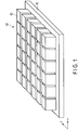
- FIG. 1 is a perspective view of the mirror device 10.
- the mirror device 10 includes a planar base material 11 and a plurality of optical elements 12 provided on the base material 11.
- the optical elements 12 are arranged, for example, in a matrix so as to extend in an x direction and a y direction that are orthogonal to each other.
- Each of the optical elements 12 has two reflective surfaces that are disposed at right angles.
- Each optical element 12 is in a cubic or rectangular parallelepiped shape.
- the base material 11 and the optical elements 12 are configured of a transparent resin.
- optical elements 12 are shown as an example; however, in actuality, a greater number of optical elements 12 are disposed.
- the number and size of the optical elements 12 can be freely set according to the specifications of the aerial display apparatus.
- a distance between two optical elements 12 can be freely set according to the specifications of the aerial display apparatus.
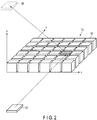
- FIG. 2 is a schematic diagram showing principles of the aerial display apparatus.
- the aerial display apparatus includes a display device 22 that displays an image on a display surface and a mirror device 10.
- the base material 11 of the mirror device 10 is not illustrated, and only the optical elements 12 are extracted for illustration, for ease of understanding of the drawing.
- the optical elements 12 are arranged on an x-y plane.
- the z direction is a direction that is orthogonal to the x and y directions, and is a height direction of the optical elements 12.
- Display light Light (display light) emitted from the display device 22 is reflected by two side surfaces of each of the optical elements 12.
- FIG. 2 the optical path of light that has been reflected by the hatched optical element 12 is extracted for illustration.
- the light emitted from the display device 22 is formed into an image at a position that is plane-symmetrical to the display device 22 with respect to the mirror device 10, and an aerial image 30 is formed at that position (hereinafter, "display position"). An observer can visually recognize the aerial image 30.
- FIG. 3 is a schematic diagram showing a state of light that is reflected twice by a single optical element 12.
- FIG. 4 is a diagram showing an optical path when the optical element 12 is viewed from the z direction.
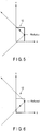
- FIG. 5 is a diagram showing an optical path when the optical element 12 is viewed from the y direction.
- FIG. 6 is a diagram showing an optical path when the optical element 12 is viewed from the x direction.
- Light that has been made incident from a bottom surface of the optical element 12 is reflected by a first side surface, further reflected by a second side surface that is at right angles to the first side surface, and then emitted from a top surface.
- the light is divided into a reflective component and a transmissive component.
- the reflective component is a component of light that has been reflected by the side surface at an angle of reflection corresponding to the angle of incidence
- the transmissive component is a component of light that is linearly transmitted through that side surface.
- FIG. 7 is a schematic diagram showing a ghost 31 displayed by the aerial display apparatus.
- the ghost 31 is an image formed by light that is reflected only once (i.e., light that is not reflected twice) by the mirror device 10.
- the ghost 31 is formed at a position that is not plane-symmetrical to the display device 22 with respect to the mirror device 10.
- FIG. 8 is a schematic diagram showing a state of light that has been reflected once by a single optical element 12.
- FIG. 9 is a diagram showing an optical path when the optical element 12 is viewed from the z direction.
- FIG. 10 is a diagram showing an optical path when the optical element 12 is viewed from the y direction.
- FIG. 11 is a diagram showing an optical path when the optical element 12 is viewed from the x direction.
- Light that has been made incident from a bottom surface of the optical element 12 is reflected by a first side surface, and is then transmitted through a second side surface that is at right angles to the first side surface.
- the light that travels along this path is formed into an image at a position that is not plane-symmetrical to the display device 22 with respect to the mirror device 10, thereby displaying a ghost 31.
- FIG. 12 is a schematic diagram showing unwanted light 32 of the aerial display apparatus.
- the unwanted light 32 is light that is not reflected at all by the mirror device 10.
- the unwanted light 32 is linearly transmitted through the mirror device 10.
- FIG. 13 is a schematic diagram showing a state of light that is not reflected at all by a single optical element 12.
- FIG. 14 is a diagram showing an optical path when the optical element 12 is viewed from the z direction.
- FIG. 15 is a diagram showing an optical path when the optical element 12 is viewed from the y direction.
- FIG. 16 is a diagram showing an optical path when the optical element 12 is viewed from the x direction.
- the light that has been made incident from the bottom surface of the optical element 12 is not reflected by the first side surface, and is linearly transmitted through the first side surface.
- the unwanted light 32 brightens the periphery of the aerial image 30. Due to the unwanted light 32, the contrast of the aerial image 30 is reduced.
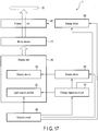
- FIG. 17 is a block diagram showing a configuration of the aerial display apparatus 1 according to the embodiment.
- FIG. 18 is a perspective view showing an optical configuration of the aerial display apparatus 1.
- FIG. 19 is a side view showing the optical configuration.
- the aerial display apparatus 1 includes a display unit 20, a mirror device 10, a display unit 40, display drivers 50 and 60, a voltage supplying circuit 70, and a control circuit 80.
- a display surface of the display unit 20 is disposed, for example, in parallel to the x-y plane.
- a principal surface of the mirror device 10 on which the optical elements 12 are arranged is disposed obliquely, for example, at 45 degrees with respect to a z direction that is orthogonal to the x-y plane.
- the principal surface of the mirror device 10 is disposed obliquely, for example, at 45 degrees with respect to the display surface of the display unit 20. That is, the angle 9 formed by the display surface of the display unit 20 and the principal surface of the mirror device 10 is, for example, 45 degrees.
- the angle ⁇ is not limited to 45 degrees, and can be set within the range of 30 degrees to 60 degrees.
- the angle formed by the principal surface of the mirror device 10 and the display surface of the display unit 40 is also set to, for example, the angle ⁇ .
- the display unit 40 is disposed, for example, in parallel to a y-z plane that is orthogonal to the x direction.
- the display unit 40 is disposed on an optical path of light emitted from the mirror device 10.
- the light emitted from the display unit 20 is reflected by the mirror device 10.
- the light that has been reflected by the mirror device 10 is transmitted through the image display surface of the display unit 40, and is formed into a real image (aerial image) 30 in the air at a position between the display unit 40 and the observer 90. That is, the display unit 40 is disposed between the mirror device 10 and the aerial image 30, and the aerial image 30 is formed above the image display surface of the display unit 40 on the side of the observer 90.
- the display unit 20 includes a light source section 21 and a display device 22.
- the light source section 21 includes a planar light source that emits planar light, and applies the planar light to the display device 22.
- the display device 22 allows the light emitted from the light source section 21 to be transmitted therethrough, and displays an image, a moving image, or the like indicating desired information. That is, the display device 22 emits light (hereinafter, "display light”) for displaying an image, a moving image, or the like as an aerial image using the light emitted from the light source section 21. Details of the display unit 20 will be described later.
- the mirror device 10 includes a plurality of optical elements 12 provided on the base material 11.
- FIG. 20 is a diagram showing a layout of a plurality of optical elements 12 on a base material 11, in which the optical elements 12 are viewed from the z direction through the base material 11.
- Each optical element 12 is in the shape of a cube or a rectangular parallelepiped having diagonal vertexes in the x and y directions, and the optical elements 12 are arranged in the x and y directions.
- each of the optical elements 12 shown in FIGS. 1 to 6 is rotated by 45 degrees with respect to the x direction, and the mirror device 10 of FIG. 20 is obtained.
- the reflective surfaces 12A and 12B of each optical element 12 are disposed at an angle of 45 degrees with respect to the x direction.
- FIG. 21 is a diagram showing an optical path when the optical element 12 shown in FIG. 20 is viewed from the z direction.
- the display light that has been made incident from a bottom surface of the optical element 12 is reflected by a reflective surface 12A, further reflected by a reflective surface 12B that is at right angles to the reflective surface 12A, and emitted from an upper surface.
- the display unit 40 is a transmissive display device that allows light that has been made incident on a rear surface to be transmitted therethrough.
- the display unit 40 includes an image display surface on which an image, a moving image, or the like, is displayed, and allows the display light emitted from the mirror device 10 to be transmitted therethrough. That is, the display unit 40 displays its own image in front of the image of the display unit 20. Details of the display unit 40 will be described later.
- the display driver 50 drives the display device 22 to display an image, a moving image, or the like on the display device 22.
- the display driver 60 drives the display unit 40 to cause the display unit 40 to display an image, a moving image, or the like on its image display surface.
- the voltage supplying circuit 70 generates voltages required to operate the light source section 21 and the display drivers 50 and 60, and supplies the generated voltages to the light source section 21 and the display drivers 50 and 60.
- the control circuit 80 controls the operation of the entire aerial display apparatus 1.
- control circuit 80 controls the light source section 21, the display drivers 50 and 60, and the voltage supplying circuit 70 to cause the display unit 40 to display an image, a moving image, or the like, and to cause the aerial image 30 to be displayed at a display position between the display unit 40 and the observer 90.
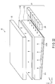
- FIG. 22 is a perspective view showing a configuration of the display unit 20.
- the display unit 20 includes a light source section 21 and a display device 22.
- the light source section 21 is configured of a side-light type (edge-light type) backlight.
- the light source section 21 includes one or more light-emitting devices 211, a light guide plate 212, a reflective sheet 213, and a diffusive sheet 214.
- the light source section 21 constitutes a surface light source by the light-emitting device 211, the light guide plate 212, the reflective sheet 213, and the diffusive sheet 214, and emits planar light to the display device 22.
- a light-emitting diode (LED), for example, is used.
- the light-emitting diode emits, for example, white light.
- the light-emitting device 211 is disposed so as to face a side surface (or an incident surface) of the light guide plate 212.
- a reflective sheet 213 is provided on a bottom surface of the light guide plate 212.
- the diffusive sheet 214 is provided on an upper surface of the light guide plate 212.
- the display device 22 is disposed on an optical path of light emitted from the diffusive sheet 214.
- light emitted from the light-emitting device 211 is made incident on a side surface of the light guide plate 212.
- a bottom surface of the light guide plate 212 functions as a surface that reflects light.
- the bottom surface of the light guide plate 212 has a plurality of reflective surfaces 212A that are arranged obliquely with respect to the horizontal direction (x-y plane), that is, has a staircase shape (corrugated pattern).
- the light that has been transmitted through the light guide plate 212 is reflected by the reflective surfaces 212A toward the diffusive sheet 214.
- the reflective sheet 213 reflects the light that has been transmitted through the bottom surface of the light guide plate 212, and returns the light to the light guide plate 212.
- the light that has been emitted from the upper surface of the light guide plate 212 and made incident on the diffusive sheet 214 is diffused by the diffusive sheet 214, and emitted from the upper surface of the diffusive sheet to the display device 22.
- the display device 22 displays an image, a moving image, or the like.
- the display device 22 allows the light received from the light source section 21 to be transmitted therethrough, and emits display light 20A for displaying an image, a moving image, or the like at a display position in the air. That is, the display device 22 modulates light from the light source section 21, and emits display light 20A for an image, a moving image, or the like.
- the display device 22 is configured using, for example, a liquid crystal display device.
- a liquid crystal display device An example of the liquid crystal display device will be described below.
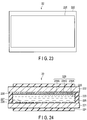
- FIG. 23 is a plan view of a liquid crystal display device as the display device 22, and
- FIG. 24 is a cross-sectional view of the liquid crystal display device.
- the display device 22 includes a TFT substrate 221 on which Thin Film Transistors (TFTs), pixel electrodes, and the like are formed, a Color Filter (CF) substrate 222 on which a color filter, a common electrode, and the like are formed and which is disposed to face the TFT substrate 221, and a liquid crystal layer 223 interposed between the TFT substrate 221 and the CF substrate 222.
- TFTs Thin Film Transistors
- CF Color Filter
- Each of the TFT substrate 221 and the CF substrate 222 is configured of a transparent substrate (e.g., a glass substrate).
- a polarizing plate 224 is disposed on a surface of the TFT substrate 221 that is opposite to the surface on which the liquid crystal layer 223 is present.
- a polarizing plate 225 is disposed on a surface of the CF substrate 222 that is opposite to the surface on which the liquid crystal layer 223 is present.
- the TFT substrate 221 is disposed so as to face the light source section 21. Illumination light that has been emitted from the light source section 21 enters the liquid crystal display device from the side of the TFT substrate 221.
- the surface of the CF substrate 222 that is opposite to a surface on which the light source section 21 is disposed is a display surface or a light emission surface of the liquid crystal display device.
- the TFT substrate 221 and the CF substrate 222 are attached to each other by a seal member 226, with a space kept therebetween.
- a liquid crystal material is sealed in a space surrounded by the TFT substrate 221, the CF substrate 222, and the seal member 226 to form a liquid crystal layer 223.
- the liquid crystal layer 23 is configured of a liquid crystal layer including liquid crystal molecules having dielectric anisotropies, and is configured of, for example, nematic liquid crystals. Liquid crystal molecules of nematic liquid crystals are electrically polarized in response to an external electric field. Examples of the liquid crystal mode that may be used include a vertical alignment (VA) mode; however, other liquid crystal modes such as a twisted nematic (TN) mode and a homogeneous mode may be used, as a matter of course.
- VA vertical alignment
- TN twisted nematic
- a plurality of switching elements such as the above-described thin-film transistors (TFTs) 227 are provided on the side of the liquid crystal layer 223 of the TFT substrate 221.
- the TFT 227 includes a gate electrode electrically connected to a scanning line, a gate insulating film provided on the gate electrode, a semiconductor layer (for example, an amorphous silicon layer) provided on the gate insulating film, and a source electrode and a drain electrode separately provided on the semiconductor layer.
- the source electrode is electrically connected to a signal line.
- An insulating layer (not shown) is provided on the TFT 227.
- a plurality of pixel electrodes 228 are provided on the insulating layer.
- a color filter 229 is provided on the side of the liquid crystal layer 223 of the CF substrate 222.
- the color filter 229 includes a plurality of coloring filters (coloring members). Specifically, a plurality of red filters 229R, a plurality of green filters 229G, and a plurality of blue filters 229B are provided.
- a general color filter is configured of red (R), green (G), and blue (B), which are the three primary colors of light.
- R, G, and B constitutes a display unit (pixel), and a single-color portion of any one of R, G, and B in a single pixel constitutes the minimal driving unit called a "sub-pixel".
- the TFT 227 and the pixel electrode 228 are provided for each sub-pixel. In the description that follows, a sub-pixel is referred to as a "pixel” unless it is particularly necessary to distinguish between a pixel and a sub-pixel.
- a black matrix (light-shielding film) (not shown) for shielding light is provided at a boundary portion of the red filter 229R, the green filter 229G, and the blue filter 229B, and a boundary portion of the pixels (sub-pixels). That is, the black matrix is formed in a mesh pattern.
- the black matrix is provided, for example, to shield unwanted light between coloring members and to improve the contrast.
- a common electrode 230 is provided on the color filter 229 and the black matrix.
- the common electrode 230 is formed in a planar shape over the entire display region of the liquid crystal display device.
- the polarizing plates 224 and 225 are provided so as to interpose the TFT substrate 221 and the CF substrate 222.
- Each of the polarizing plates 224 and 225 is configured of a linear polarizer and a 1/4-wavelength plate.
- the pixel electrode 228 and the common electrode 230 are formed of transparent electrodes using, for example, indium tin oxides (ITO).
- ITO indium tin oxides
- the display unit 40 is configured of a self-luminous and transmissive display device.
- the display unit 40 displays an image, a moving image, or the like by using light emitted by itself, and allows the display light from the mirror device 10 to be transmitted therethrough.
- various transmissive display devices may be used, such as a transparent organic electroluminescence (EL) display device, a transparent inorganic EL display device, and a transmissive liquid crystal display device with a side-light type backlight.
- EL transparent organic electroluminescence
- a transparent inorganic EL display device a transmissive liquid crystal display device with a side-light type backlight.
- a transparent organic EL display device will be described as an example of the self-luminous and transmissive display device.
- FIG. 25 is a cross-sectional view of a transparent organic EL display device as the display unit 40.
- the transparent organic EL display device includes substrates 41 and 42, a plurality of switching elements such as TFTs 43, an insulating layer 44, a pixel electrode 45, an organic layer 46, a common electrode 47, and a color filter 48, which are provided between the substrates 41 and 42.
- Each of the substrates 41 and 42 is configured of a transparent substrate (e.g., a glass substrate or plastic) or a transparent film.
- a plurality of TFTs 43 are provided on the substrate 41.
- Each TFT 43 includes a gate electrode 43A electrically connected to a scanning line, a gate insulating film 43B provided on the gate electrode 43A, a semiconductor layer (e.g., an amorphous silicon layer) 43C provided on the gate insulating film 43B, and a source electrode 43D and a drain electrode 43E separately provided on the semiconductor layer 43C.
- the source electrode 43D is electrically connected to a signal line.
- An insulating layer 44 is provided on the TFT 43.
- a plurality of pixel electrodes 45 are provided on the insulating layer 44. Each pixel electrode 45 is electrically connected to the drain electrode 43E of the TFT 43 via a contact plug.
- An organic layer 46 is provided on each pixel electrode 45.
- a common electrode 47 is provided on the organic layers 46.
- a color filter 48 is provided above the common electrode 47 so as to correspond to each organic layer 46.
- a substrate 42 is provided on the color filter 48.
- a sealed air layer is provided between the common electrode 47 and the substrate 42.
- the transparent organic EL display device includes a light-emitting region 40B that emits light 40A, and a transmissive region 40C that allows a display light 20A to be transmitted therethrough.
- the TFT 43, the pixel electrode 45, the organic layer 46, the common electrode 47, and the color filter 48 are disposed between the substrate 41 and the substrate 42, and light 40A can be emitted from the organic layer 46.
- a common electrode 47 is disposed in the transmissive region 40C. Since the common electrode 47 is configured of a transparent electrode (e.g., ITO), the display light 20A that has been made incident on the substrate 41 of the transmissive region 40C is passed through the common electrode 47, and is emitted from the substrate 42.
- a transparent electrode e.g., ITO
- a plurality of TFTs 43 are controlled to an ON state or an OFF state by the control circuit 80 via the display driver 60.
- the TFT 43 When the TFT 43 is turned on, a voltage is applied to the pixel electrode 45, and a potential difference is generated between the pixel electrode 45 and the common electrode 47, causing light to be emitted from the organic layer 46.
- the TFT 43 When the TFT 43 is turned off, a voltage is not applied to the pixel electrode 45, and light is not emitted from the organic layer 46.
- the transmissive region 40C provided between the light-emitting regions 40B allows the display light 20A that has been emitted from the mirror device 10 to be transmitted therethrough.
- the display light 20A that has been transmitted through the transmissive region 40C is formed into an aerial image 30 at the display position.
- FIG. 19 is a diagram showing an optical configuration of the aerial display apparatus 1, as described above.
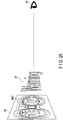
- FIG. 26 is a diagram showing a display example displayed on an aerial display apparatus 1 for vehicle use.
- the display light 20A is emitted from the display unit 20 to the mirror device 10.
- the display light 20A that has been made incident on the mirror device 10 is reflected by the optical element 12 included in the mirror device 10, as described with reference to FIG. 21 .
- the light that has been reflected by the optical element 12 is transmitted through the image display surface of the display unit 40, and is formed into an aerial image 30 at the display position between the display unit 40 and the observer 90. That is, the display light 20A emitted from the display unit 20 is formed into an image at a display position that is plane-symmetrical to the image displayed on the display device 20 with respect to the mirror device 10, and the aerial image 30 is displayed at the display position, as shown in FIG. 26 . Moreover, an image 40D is displayed on the image display surface of the display unit 40.
- the aerial image 30 is displayed above the image 40D of the display unit 40.
- the observer 90 can visually recognize a display in which the image 40D and the aerial image 30 overlap each other. For example, as shown in FIG. 26 , the observer 90 can visually recognize an overlapping display of a speedometer and a tachometer displayed as the image 40D and a warning display displayed as the aerial image 30.
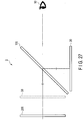
- FIG. 27 is a schematic diagram showing an optical configuration of an aerial display apparatus according to a comparative example.
- a semitransparent mirror 100 is arranged obliquely on an optical path of the light emitted from the display unit 20.
- a display unit 200 is arranged at the back (or a rear direction) of the semitransparent mirror 100.
- the light emitted from the display unit 20 is reflected by the semitransparent mirror 100 in the direction of the observer 90.
- the observer 90 visually recognizes the aerial image 30 at the back of the semitransparent mirror 100 with the light that has been reflected by the semitransparent mirror 100.
- an image is displayed on the display unit 200 disposed at the back of the aerial image 30. Thereby, the observer 90 can visually recognize a display in which an image of the display unit 200 and the aerial image 30 overlap each other.
- the light from the display unit 20 is reflected by the semitransparent mirror 100, and is formed into an aerial image 30.
- the aerial image 30 is displayed at a position that is plane-symmetrical to the display unit 20 via the semitransparent mirror 100.
- the aerial image 30 and the image of the display unit 200 are arranged at the back of the semitransparent mirror 100.
- the observer 90 who visually recognizes the image of the display unit 200 and the aerial image 30 via the semitransparent mirror 100, might not visually recognize these images favorably.
- the aerial display apparatus comprises a display unit (display device) 20 which includes a display surface on which a first image is displayed and which emits display light from the display surface; a mirror device 10 which is disposed obliquely with respect to the display surface of the display unit 20, which reflects the display light emitted from the display unit 20, and which forms an aerial image 30 at a position that is plane-symmetrical to the display unit 20; and a display unit (display device) 40 which is arranged between the mirror device 10 and the aerial image 30, which allows the display light that has been reflected by the mirror device 10 to be transmitted therethough, and which displays a second image.
- a display unit (display device) 20 which includes a display surface on which a first image is displayed and which emits display light from the display surface
- a mirror device 10 which is disposed obliquely with respect to the display surface of the display unit 20, which reflects the display light emitted from the display unit 20, and which forms an aerial image 30 at a position that is plane-symmetrical to the display unit
- the display light emitted from the display unit 20 is reflected by the mirror device 10, transmitted through the display surface of the display unit 40, and formed into an aerial image 30 at a position between the display unit 40 and the observer 90.
- a second image is displayed on the display unit 40.
- the aerial image 30 is displayed above the second image of the display unit 40, and the second image and the aerial image 30 are displayed in an overlapping manner.
- the observer 90 can visually recognize the overlapping display of the second image and the aerial image 30 directly, without using a semitransparent mirror or the like.
- the aerial display apparatus 1 of the embodiment described above it is possible to display an aerial image above an image display surface of the display unit (display device), and to improve the display quality of both an image on the image display surface and the aerial image.
- the aerial display apparatus 1 of the embodiment is capable of displaying an aerial image in front of the image display surface of the display unit, as viewed from the observer, thus improving the visibility to the observer of the image on the image display surface and the aerial image.
- an example of a product field in which the aerial display apparatus is used will be described below.
- a conventional mechanical meter type is being replaced with an image display surface such as an electronic display capable of displaying various types of information.
- an aerial display image By presenting an aerial display image in front of the image display surface, a new display means can be proposed.
- a behavior of a driver who drives an automobile will be taken as an example. The driver checks the instrument panel while checking the front and surrounding conditions through the windshield to grasp the vehicle conditions (e.g., the vehicle body speed, the engine or the motor rotation speed, the fuel remaining amount or the power condition, or the like).
- the driver's attention can be more effectively called by making an attention-calling display in a space in front of (on the driver side of) the image display surface of the instrument panel, rather than on the same plane as the image display surface of the instrument panel.
- an effect of preventing an unfortunate accident such as a traffic accident can be expected.
- 1...Aerial display apparatus 10...Mirror device, 11...Base material, 12...Optical element, 12A, 12B...Reflective surface, 20...Display unit, 20A...Display light, 21...Light source section, 22...Display device, 30...Aerial image, 40...Display unit, 40A...Light, 40B...Light-emitting region, 40C...Transmissive region, 40D...Image, 50, 60...Display driver, 70...Voltage supplying circuit, 80...Control circuit, 90...Observer, 211...Light-emitting device, 212...Light guide plate, 212A...Reflective surface, 213...Reflective sheet, 214...Diffusive sheet.
Landscapes
- Physics & Mathematics (AREA)
- General Physics & Mathematics (AREA)
- Optics & Photonics (AREA)
- Engineering & Computer Science (AREA)
- Theoretical Computer Science (AREA)
- Business, Economics & Management (AREA)
- Accounting & Taxation (AREA)
- Marketing (AREA)
- Liquid Crystal (AREA)
- Electroluminescent Light Sources (AREA)
- Testing, Inspecting, Measuring Of Stereoscopic Televisions And Televisions (AREA)
- Devices For Indicating Variable Information By Combining Individual Elements (AREA)
- Optical Elements Other Than Lenses (AREA)
Abstract
Description
- The present invention relates to an aerial display apparatus.
- An aerial display apparatus capable of displaying an image, a moving image, etc. as an aerial image has been studied and is expected as a new human-machine interface. The aerial display apparatus reflects light emitted from a display device and forms a real image (hereinafter, an "aerial image") in the air using, for example, a dihedral corner reflector array in which dihedral corner reflectors are arranged in an array (see, for example, Patent Document 1). In the display method using the dihedral corner reflector array, aberration does not occur, and a real image is displayed at a plane-symmetrical position.
- Patent Document 1: Jpn. Pat. Appln. KOKAI Publication No.
2017-67933 - An aerial display apparatus capable of displaying an aerial image above an image display surface of a display device and improving the display quality of both an image on the image display surface and the aerial image is provided.
- An aerial display apparatus according to an embodiment includes: a first display device which includes a display surface on which a first image is displayed, and which emits display light from the display surface; a mirror device which is disposed obliquely with respect to the display surface of the first display device, which reflects the display light that has been emitted from the first display device to form an aerial image at a position that is plane-symmetrical to the first display device; and a second display device which is disposed between the mirror device and the aerial image, which allows the display light that has been reflected by the mirror device to be transmitted therethough, and which displays a second image.
-
-
FIG. 1 is a perspective view of a mirror device. -
FIG. 2 is a schematic diagram showing principles of an aerial display apparatus. -
FIG. 3 is a schematic diagram showing a state of light that is reflected twice by a single optical element of the mirror device. -
FIG. 4 is a diagram showing an optical path when the optical element shown inFIG. 3 is viewed from a z direction. -
FIG. 5 is a diagram showing an optical path when the optical element shown inFIG. 3 is viewed from a y direction. -
FIG. 6 is a diagram showing an optical path when the optical element shown inFIG. 3 is viewed from an x direction. -
FIG. 7 is a schematic diagram showing a ghost displayed by the aerial display apparatus. -
FIG. 8 is a schematic diagram showing a state of light that is reflected once by a single optical element. -
FIG. 9 is a diagram showing an optical path when the optical element shown inFIG. 8 is viewed from the z direction. -
FIG. 10 is a diagram showing an optical path when the optical element shown inFIG. 8 is viewed from the y direction. -
FIG. 11 is a diagram showing an optical path when the optical element shown inFIG. 8 is viewed from the x direction. -
FIG. 12 is a schematic diagram showing unwanted light of the aerial display apparatus. -
FIG. 13 is a schematic diagram showing a state of light that is not reflected at all by a single optical element. -
FIG. 14 is a diagram showing an optical path when the optical element shown inFIG. 13 is viewed from the z direction. -
FIG. 15 is a diagram showing an optical path when the optical element shown inFIG. 13 is viewed from the y direction. -
FIG. 16 is a diagram showing an optical path when the optical element shown inFIG. 13 is viewed from the x direction. -
FIG. 17 is a block diagram showing a configuration of the aerial display apparatus according to an embodiment. -
FIG. 18 is a perspective view showing an optical configuration of the aerial display apparatus according to the embodiment. -
FIG. 19 is a side view showing an optical configuration of the aerial display apparatus according to the embodiment. -
FIG. 20 is a layout diagram of an optical element in a mirror device in the aerial display apparatus. -
FIG. 21 is a diagram showing an optical path when the optical element shown inFIG. 20 is viewed from the z direction. -
FIG. 22 is a perspective view showing a configuration of a display unit in the aerial display apparatus. -
FIG. 23 is a plan view of a liquid crystal display device as a display device in the display unit. -
FIG. 24 is a cross-sectional view of the liquid crystal display device shown inFIG. 23 . -
FIG. 25 is a cross-sectional view of a transparent organic EL display device as a display unit. -
FIG. 26 is a diagram showing a display example displayed on an aerial display apparatus for vehicle use. -
FIG. 27 is a schematic diagram showing an optical configuration of an aerial display apparatus according to a comparative example. - Hereinafter, embodiments will be described with reference to the drawings. The drawings are schematic or conceptual, and the dimensions, ratios, and the like of each drawing are not necessarily the same as the actual ones. Even when the same portions are shown in the drawings, the dimensional relationship and the ratio may be different. In particular, several embodiments described below exemplify an apparatus and a method for embodying the technical idea of the present invention, and the technical idea of the present invention is not specified by the shape, structure, arrangement, or the like of the components. In the following description, elements having the same function and configuration will be denoted by the same reference numerals, and redundant descriptions will be made only when necessary.
- Before describing the aerial display apparatus of the present embodiment, the principles of the aerial display apparatus will be described.
- An aerial display apparatus is configured to form an image of light emitted from a display surface of, for example, a liquid crystal display in the air, using an aerial imaging device (mirror device) such as a dihedral corner reflector.
- A configuration of a
mirror device 10 used in the aerial display apparatus will be described.FIG. 1 is a perspective view of themirror device 10. - The
mirror device 10 includes aplanar base material 11 and a plurality ofoptical elements 12 provided on thebase material 11. Theoptical elements 12 are arranged, for example, in a matrix so as to extend in an x direction and a y direction that are orthogonal to each other. Each of theoptical elements 12 has two reflective surfaces that are disposed at right angles. Eachoptical element 12 is in a cubic or rectangular parallelepiped shape. Thebase material 11 and theoptical elements 12 are configured of a transparent resin. - In
FIG. 1 , 36 (= 6 × 6)optical elements 12 are shown as an example; however, in actuality, a greater number ofoptical elements 12 are disposed. The number and size of theoptical elements 12 can be freely set according to the specifications of the aerial display apparatus. A distance between twooptical elements 12 can be freely set according to the specifications of the aerial display apparatus. -
FIG. 2 is a schematic diagram showing principles of the aerial display apparatus. The aerial display apparatus includes adisplay device 22 that displays an image on a display surface and amirror device 10. InFIG. 2 , thebase material 11 of themirror device 10 is not illustrated, and only theoptical elements 12 are extracted for illustration, for ease of understanding of the drawing. Theoptical elements 12 are arranged on an x-y plane. The z direction is a direction that is orthogonal to the x and y directions, and is a height direction of theoptical elements 12. - Light (display light) emitted from the
display device 22 is reflected by two side surfaces of each of theoptical elements 12. InFIG. 2 , the optical path of light that has been reflected by the hatchedoptical element 12 is extracted for illustration. The light emitted from thedisplay device 22 is formed into an image at a position that is plane-symmetrical to thedisplay device 22 with respect to themirror device 10, and anaerial image 30 is formed at that position (hereinafter, "display position"). An observer can visually recognize theaerial image 30. -
FIG. 3 is a schematic diagram showing a state of light that is reflected twice by a singleoptical element 12.FIG. 4 is a diagram showing an optical path when theoptical element 12 is viewed from the z direction.FIG. 5 is a diagram showing an optical path when theoptical element 12 is viewed from the y direction.FIG. 6 is a diagram showing an optical path when theoptical element 12 is viewed from the x direction. - Light that has been made incident from a bottom surface of the
optical element 12 is reflected by a first side surface, further reflected by a second side surface that is at right angles to the first side surface, and then emitted from a top surface. - It should be noted that not all the light components of light that has been made incident on a given side surface of the
optical element 12 are reflected by that side surface, and the light is divided into a reflective component and a transmissive component. The reflective component is a component of light that has been reflected by the side surface at an angle of reflection corresponding to the angle of incidence, and the transmissive component is a component of light that is linearly transmitted through that side surface. - Next, a ghost that is formed at an unintended position will be described. A ghost is a double image that appears in the vicinity of the
aerial image 30.FIG. 7 is a schematic diagram showing aghost 31 displayed by the aerial display apparatus. - The
ghost 31 is an image formed by light that is reflected only once (i.e., light that is not reflected twice) by themirror device 10. Theghost 31 is formed at a position that is not plane-symmetrical to thedisplay device 22 with respect to themirror device 10. -
FIG. 8 is a schematic diagram showing a state of light that has been reflected once by a singleoptical element 12.FIG. 9 is a diagram showing an optical path when theoptical element 12 is viewed from the z direction.FIG. 10 is a diagram showing an optical path when theoptical element 12 is viewed from the y direction.FIG. 11 is a diagram showing an optical path when theoptical element 12 is viewed from the x direction. - Light that has been made incident from a bottom surface of the
optical element 12 is reflected by a first side surface, and is then transmitted through a second side surface that is at right angles to the first side surface. The light that travels along this path is formed into an image at a position that is not plane-symmetrical to thedisplay device 22 with respect to themirror device 10, thereby displaying aghost 31. - Next, unwanted light will be described. Unwanted light is a light component that does not contribute to formation of a real image.
FIG. 12 is a schematic diagram showingunwanted light 32 of the aerial display apparatus. - The
unwanted light 32 is light that is not reflected at all by themirror device 10. Theunwanted light 32 is linearly transmitted through themirror device 10. -
FIG. 13 is a schematic diagram showing a state of light that is not reflected at all by a singleoptical element 12.FIG. 14 is a diagram showing an optical path when theoptical element 12 is viewed from the z direction.FIG. 15 is a diagram showing an optical path when theoptical element 12 is viewed from the y direction.FIG. 16 is a diagram showing an optical path when theoptical element 12 is viewed from the x direction. - The light that has been made incident from the bottom surface of the
optical element 12 is not reflected by the first side surface, and is linearly transmitted through the first side surface. - The
unwanted light 32 brightens the periphery of theaerial image 30. Due to theunwanted light 32, the contrast of theaerial image 30 is reduced. - Next, an aerial display apparatus according to an embodiment using the above-described principles will be described.
- A configuration of the
aerial display apparatus 1 of the embodiment will be described with reference toFIGS. 17 and18 .FIG. 17 is a block diagram showing a configuration of theaerial display apparatus 1 according to the embodiment.FIG. 18 is a perspective view showing an optical configuration of theaerial display apparatus 1.FIG. 19 is a side view showing the optical configuration. - As shown in
FIGS. 17 to 19 , theaerial display apparatus 1 includes adisplay unit 20, amirror device 10, adisplay unit 40,display drivers voltage supplying circuit 70, and acontrol circuit 80. - As shown in
FIGS. 18 and19 , a display surface of thedisplay unit 20 is disposed, for example, in parallel to the x-y plane. As shown inFIG. 19 , a principal surface of themirror device 10 on which theoptical elements 12 are arranged is disposed obliquely, for example, at 45 degrees with respect to a z direction that is orthogonal to the x-y plane. In other words, the principal surface of themirror device 10 is disposed obliquely, for example, at 45 degrees with respect to the display surface of thedisplay unit 20. That is, the angle 9 formed by the display surface of thedisplay unit 20 and the principal surface of themirror device 10 is, for example, 45 degrees. The angle θ is not limited to 45 degrees, and can be set within the range of 30 degrees to 60 degrees. - The angle formed by the principal surface of the
mirror device 10 and the display surface of thedisplay unit 40 is also set to, for example, the angle θ. In the example ofFIG. 18 , thedisplay unit 40 is disposed, for example, in parallel to a y-z plane that is orthogonal to the x direction. Thedisplay unit 40 is disposed on an optical path of light emitted from themirror device 10. - The light emitted from the
display unit 20 is reflected by themirror device 10. The light that has been reflected by themirror device 10 is transmitted through the image display surface of thedisplay unit 40, and is formed into a real image (aerial image) 30 in the air at a position between thedisplay unit 40 and theobserver 90. That is, thedisplay unit 40 is disposed between themirror device 10 and theaerial image 30, and theaerial image 30 is formed above the image display surface of thedisplay unit 40 on the side of theobserver 90. - The
display unit 20 includes alight source section 21 and adisplay device 22. Thelight source section 21 includes a planar light source that emits planar light, and applies the planar light to thedisplay device 22. Thedisplay device 22 allows the light emitted from thelight source section 21 to be transmitted therethrough, and displays an image, a moving image, or the like indicating desired information. That is, thedisplay device 22 emits light (hereinafter, "display light") for displaying an image, a moving image, or the like as an aerial image using the light emitted from thelight source section 21. Details of thedisplay unit 20 will be described later. - As described above, the
mirror device 10 includes a plurality ofoptical elements 12 provided on thebase material 11.FIG. 20 is a diagram showing a layout of a plurality ofoptical elements 12 on abase material 11, in which theoptical elements 12 are viewed from the z direction through thebase material 11. Eachoptical element 12 is in the shape of a cube or a rectangular parallelepiped having diagonal vertexes in the x and y directions, and theoptical elements 12 are arranged in the x and y directions. In other words, each of theoptical elements 12 shown inFIGS. 1 to 6 is rotated by 45 degrees with respect to the x direction, and themirror device 10 ofFIG. 20 is obtained. As shown inFIG. 20 , thereflective surfaces optical element 12 are disposed at an angle of 45 degrees with respect to the x direction. -
FIG. 21 is a diagram showing an optical path when theoptical element 12 shown inFIG. 20 is viewed from the z direction. The display light that has been made incident from a bottom surface of theoptical element 12 is reflected by areflective surface 12A, further reflected by areflective surface 12B that is at right angles to thereflective surface 12A, and emitted from an upper surface. - The
display unit 40 is a transmissive display device that allows light that has been made incident on a rear surface to be transmitted therethrough. Thedisplay unit 40 includes an image display surface on which an image, a moving image, or the like, is displayed, and allows the display light emitted from themirror device 10 to be transmitted therethrough. That is, thedisplay unit 40 displays its own image in front of the image of thedisplay unit 20. Details of thedisplay unit 40 will be described later. - The
display driver 50 drives thedisplay device 22 to display an image, a moving image, or the like on thedisplay device 22. Thedisplay driver 60 drives thedisplay unit 40 to cause thedisplay unit 40 to display an image, a moving image, or the like on its image display surface. Thevoltage supplying circuit 70 generates voltages required to operate thelight source section 21 and thedisplay drivers light source section 21 and thedisplay drivers control circuit 80 controls the operation of the entireaerial display apparatus 1. That is, thecontrol circuit 80 controls thelight source section 21, thedisplay drivers voltage supplying circuit 70 to cause thedisplay unit 40 to display an image, a moving image, or the like, and to cause theaerial image 30 to be displayed at a display position between thedisplay unit 40 and theobserver 90. - Next, the
display unit 20 in theaerial display apparatus 1 will be described with reference toFIG. 22. FIG. 22 is a perspective view showing a configuration of thedisplay unit 20. As described above, thedisplay unit 20 includes alight source section 21 and adisplay device 22. - The
light source section 21 is configured of a side-light type (edge-light type) backlight. Thelight source section 21 includes one or more light-emittingdevices 211, alight guide plate 212, areflective sheet 213, and adiffusive sheet 214. Thelight source section 21 constitutes a surface light source by the light-emittingdevice 211, thelight guide plate 212, thereflective sheet 213, and thediffusive sheet 214, and emits planar light to thedisplay device 22. - For the light-emitting
device 211, a light-emitting diode (LED), for example, is used. The light-emitting diode emits, for example, white light. The light-emittingdevice 211 is disposed so as to face a side surface (or an incident surface) of thelight guide plate 212. Areflective sheet 213 is provided on a bottom surface of thelight guide plate 212. Thediffusive sheet 214 is provided on an upper surface of thelight guide plate 212. Thedisplay device 22 is disposed on an optical path of light emitted from thediffusive sheet 214. - As shown in
FIG. 22 , light emitted from the light-emittingdevice 211 is made incident on a side surface of thelight guide plate 212. A bottom surface of thelight guide plate 212 functions as a surface that reflects light. The bottom surface of thelight guide plate 212 has a plurality ofreflective surfaces 212A that are arranged obliquely with respect to the horizontal direction (x-y plane), that is, has a staircase shape (corrugated pattern). The light that has been transmitted through thelight guide plate 212 is reflected by thereflective surfaces 212A toward thediffusive sheet 214. Thereflective sheet 213 reflects the light that has been transmitted through the bottom surface of thelight guide plate 212, and returns the light to thelight guide plate 212. The light that has been emitted from the upper surface of thelight guide plate 212 and made incident on thediffusive sheet 214 is diffused by thediffusive sheet 214, and emitted from the upper surface of the diffusive sheet to thedisplay device 22. - The
display device 22 displays an image, a moving image, or the like. Thedisplay device 22 allows the light received from thelight source section 21 to be transmitted therethrough, and emits display light 20A for displaying an image, a moving image, or the like at a display position in the air. That is, thedisplay device 22 modulates light from thelight source section 21, and emits display light 20A for an image, a moving image, or the like. - The
display device 22 is configured using, for example, a liquid crystal display device. An example of the liquid crystal display device will be described below.FIG. 23 is a plan view of a liquid crystal display device as thedisplay device 22, andFIG. 24 is a cross-sectional view of the liquid crystal display device. - The
display device 22 includes aTFT substrate 221 on which Thin Film Transistors (TFTs), pixel electrodes, and the like are formed, a Color Filter (CF)substrate 222 on which a color filter, a common electrode, and the like are formed and which is disposed to face theTFT substrate 221, and aliquid crystal layer 223 interposed between theTFT substrate 221 and theCF substrate 222. - Each of the
TFT substrate 221 and theCF substrate 222 is configured of a transparent substrate (e.g., a glass substrate). Apolarizing plate 224 is disposed on a surface of theTFT substrate 221 that is opposite to the surface on which theliquid crystal layer 223 is present. Furthermore, apolarizing plate 225 is disposed on a surface of theCF substrate 222 that is opposite to the surface on which theliquid crystal layer 223 is present. - The
TFT substrate 221 is disposed so as to face thelight source section 21. Illumination light that has been emitted from thelight source section 21 enters the liquid crystal display device from the side of theTFT substrate 221. The surface of theCF substrate 222 that is opposite to a surface on which thelight source section 21 is disposed is a display surface or a light emission surface of the liquid crystal display device. - The
TFT substrate 221 and theCF substrate 222 are attached to each other by aseal member 226, with a space kept therebetween. A liquid crystal material is sealed in a space surrounded by theTFT substrate 221, theCF substrate 222, and theseal member 226 to form aliquid crystal layer 223. - In the liquid crystal material contained in the
liquid crystal layer 223, the alignment of the liquid crystal molecules is operated in accordance with an electric field applied between theTFT substrate 221 and theCF substrate 222, resulting in a change in optical characteristics. The liquid crystal layer 23 is configured of a liquid crystal layer including liquid crystal molecules having dielectric anisotropies, and is configured of, for example, nematic liquid crystals. Liquid crystal molecules of nematic liquid crystals are electrically polarized in response to an external electric field. Examples of the liquid crystal mode that may be used include a vertical alignment (VA) mode; however, other liquid crystal modes such as a twisted nematic (TN) mode and a homogeneous mode may be used, as a matter of course. - A plurality of switching elements, such as the above-described thin-film transistors (TFTs) 227 are provided on the side of the
liquid crystal layer 223 of theTFT substrate 221. TheTFT 227 includes a gate electrode electrically connected to a scanning line, a gate insulating film provided on the gate electrode, a semiconductor layer (for example, an amorphous silicon layer) provided on the gate insulating film, and a source electrode and a drain electrode separately provided on the semiconductor layer. The source electrode is electrically connected to a signal line. An insulating layer (not shown) is provided on theTFT 227. A plurality of pixel electrodes 228 are provided on the insulating layer. - A
color filter 229 is provided on the side of theliquid crystal layer 223 of theCF substrate 222. Thecolor filter 229 includes a plurality of coloring filters (coloring members). Specifically, a plurality ofred filters 229R, a plurality ofgreen filters 229G, and a plurality ofblue filters 229B are provided. A general color filter is configured of red (R), green (G), and blue (B), which are the three primary colors of light. A set of three adjacent colors, R, G, and B constitutes a display unit (pixel), and a single-color portion of any one of R, G, and B in a single pixel constitutes the minimal driving unit called a "sub-pixel". TheTFT 227 and the pixel electrode 228 are provided for each sub-pixel. In the description that follows, a sub-pixel is referred to as a "pixel" unless it is particularly necessary to distinguish between a pixel and a sub-pixel. - A black matrix (light-shielding film) (not shown) for shielding light is provided at a boundary portion of the
red filter 229R, thegreen filter 229G, and theblue filter 229B, and a boundary portion of the pixels (sub-pixels). That is, the black matrix is formed in a mesh pattern. The black matrix is provided, for example, to shield unwanted light between coloring members and to improve the contrast. - A
common electrode 230 is provided on thecolor filter 229 and the black matrix. Thecommon electrode 230 is formed in a planar shape over the entire display region of the liquid crystal display device. - The
polarizing plates TFT substrate 221 and theCF substrate 222. Each of thepolarizing plates - The pixel electrode 228 and the
common electrode 230 are formed of transparent electrodes using, for example, indium tin oxides (ITO). - The
display unit 40 is configured of a self-luminous and transmissive display device. Thedisplay unit 40 displays an image, a moving image, or the like by using light emitted by itself, and allows the display light from themirror device 10 to be transmitted therethrough. For thedisplay unit 40, various transmissive display devices may be used, such as a transparent organic electroluminescence (EL) display device, a transparent inorganic EL display device, and a transmissive liquid crystal display device with a side-light type backlight. Herein, a transparent organic EL display device will be described as an example of the self-luminous and transmissive display device. -
FIG. 25 is a cross-sectional view of a transparent organic EL display device as thedisplay unit 40. The transparent organic EL display device includessubstrates TFTs 43, an insulatinglayer 44, apixel electrode 45, anorganic layer 46, acommon electrode 47, and acolor filter 48, which are provided between thesubstrates - Each of the
substrates TFTs 43 are provided on thesubstrate 41. EachTFT 43 includes agate electrode 43A electrically connected to a scanning line, agate insulating film 43B provided on thegate electrode 43A, a semiconductor layer (e.g., an amorphous silicon layer) 43C provided on thegate insulating film 43B, and asource electrode 43D and adrain electrode 43E separately provided on thesemiconductor layer 43C. Thesource electrode 43D is electrically connected to a signal line. - An insulating
layer 44 is provided on theTFT 43. A plurality ofpixel electrodes 45 are provided on the insulatinglayer 44. Eachpixel electrode 45 is electrically connected to thedrain electrode 43E of theTFT 43 via a contact plug. Anorganic layer 46 is provided on eachpixel electrode 45. Acommon electrode 47 is provided on the organic layers 46. Acolor filter 48 is provided above thecommon electrode 47 so as to correspond to eachorganic layer 46. Asubstrate 42 is provided on thecolor filter 48. A sealed air layer is provided between thecommon electrode 47 and thesubstrate 42. - The transparent organic EL display device includes a light-emitting
region 40B that emits light 40A, and atransmissive region 40C that allows adisplay light 20A to be transmitted therethrough. In the light-emittingregion 40B, theTFT 43, thepixel electrode 45, theorganic layer 46, thecommon electrode 47, and thecolor filter 48 are disposed between thesubstrate 41 and thesubstrate 42, and light 40A can be emitted from theorganic layer 46. In thetransmissive region 40C, acommon electrode 47 is disposed. Since thecommon electrode 47 is configured of a transparent electrode (e.g., ITO), thedisplay light 20A that has been made incident on thesubstrate 41 of thetransmissive region 40C is passed through thecommon electrode 47, and is emitted from thesubstrate 42. - In the
display unit 40, a plurality ofTFTs 43 are controlled to an ON state or an OFF state by thecontrol circuit 80 via thedisplay driver 60. When theTFT 43 is turned on, a voltage is applied to thepixel electrode 45, and a potential difference is generated between thepixel electrode 45 and thecommon electrode 47, causing light to be emitted from theorganic layer 46. When theTFT 43 is turned off, a voltage is not applied to thepixel electrode 45, and light is not emitted from theorganic layer 46. - The
transmissive region 40C provided between the light-emittingregions 40B allows thedisplay light 20A that has been emitted from themirror device 10 to be transmitted therethrough. Thedisplay light 20A that has been transmitted through thetransmissive region 40C is formed into anaerial image 30 at the display position. - Next, a display operation of the aerial display apparatus according to the embodiment will be described with reference to
FIGS. 19 and26 .FIG. 19 is a diagram showing an optical configuration of theaerial display apparatus 1, as described above.FIG. 26 is a diagram showing a display example displayed on anaerial display apparatus 1 for vehicle use. - As shown in
FIG. 19 , thedisplay light 20A is emitted from thedisplay unit 20 to themirror device 10. Thedisplay light 20A that has been made incident on themirror device 10 is reflected by theoptical element 12 included in themirror device 10, as described with reference toFIG. 21 . The light that has been reflected by theoptical element 12 is transmitted through the image display surface of thedisplay unit 40, and is formed into anaerial image 30 at the display position between thedisplay unit 40 and theobserver 90. That is, thedisplay light 20A emitted from thedisplay unit 20 is formed into an image at a display position that is plane-symmetrical to the image displayed on thedisplay device 20 with respect to themirror device 10, and theaerial image 30 is displayed at the display position, as shown inFIG. 26 . Moreover, animage 40D is displayed on the image display surface of thedisplay unit 40. - Thereby, the
aerial image 30 is displayed above theimage 40D of thedisplay unit 40. Theobserver 90 can visually recognize a display in which theimage 40D and theaerial image 30 overlap each other. For example, as shown inFIG. 26 , theobserver 90 can visually recognize an overlapping display of a speedometer and a tachometer displayed as theimage 40D and a warning display displayed as theaerial image 30. - Before describing the advantageous effects of the embodiment in detail, an aerial display apparatus of a comparative example will be described below.
FIG. 27 is a schematic diagram showing an optical configuration of an aerial display apparatus according to a comparative example. In the comparative example, asemitransparent mirror 100 is arranged obliquely on an optical path of the light emitted from thedisplay unit 20. Moreover, adisplay unit 200 is arranged at the back (or a rear direction) of thesemitransparent mirror 100. The light emitted from thedisplay unit 20 is reflected by thesemitransparent mirror 100 in the direction of theobserver 90. Theobserver 90 visually recognizes theaerial image 30 at the back of thesemitransparent mirror 100 with the light that has been reflected by thesemitransparent mirror 100. Moreover, an image is displayed on thedisplay unit 200 disposed at the back of theaerial image 30. Thereby, theobserver 90 can visually recognize a display in which an image of thedisplay unit 200 and theaerial image 30 overlap each other. - In the comparative example, the light from the
display unit 20 is reflected by thesemitransparent mirror 100, and is formed into anaerial image 30. Accordingly, theaerial image 30 is displayed at a position that is plane-symmetrical to thedisplay unit 20 via thesemitransparent mirror 100. Thus, theaerial image 30 and the image of thedisplay unit 200 are arranged at the back of thesemitransparent mirror 100. As a result, theobserver 90, who visually recognizes the image of thedisplay unit 200 and theaerial image 30 via thesemitransparent mirror 100, might not visually recognize these images favorably. - The aerial display apparatus according to the embodiment comprises a display unit (display device) 20 which includes a display surface on which a first image is displayed and which emits display light from the display surface; a
mirror device 10 which is disposed obliquely with respect to the display surface of thedisplay unit 20, which reflects the display light emitted from thedisplay unit 20, and which forms anaerial image 30 at a position that is plane-symmetrical to thedisplay unit 20; and a display unit (display device) 40 which is arranged between themirror device 10 and theaerial image 30, which allows the display light that has been reflected by themirror device 10 to be transmitted therethough, and which displays a second image. - With such a configuration, the display light emitted from the
display unit 20 is reflected by themirror device 10, transmitted through the display surface of thedisplay unit 40, and formed into anaerial image 30 at a position between thedisplay unit 40 and theobserver 90. Moreover, a second image is displayed on thedisplay unit 40. Thereby, theaerial image 30 is displayed above the second image of thedisplay unit 40, and the second image and theaerial image 30 are displayed in an overlapping manner. Theobserver 90 can visually recognize the overlapping display of the second image and theaerial image 30 directly, without using a semitransparent mirror or the like. - According to the
aerial display apparatus 1 of the embodiment described above, it is possible to display an aerial image above an image display surface of the display unit (display device), and to improve the display quality of both an image on the image display surface and the aerial image. In other words, theaerial display apparatus 1 of the embodiment is capable of displaying an aerial image in front of the image display surface of the display unit, as viewed from the observer, thus improving the visibility to the observer of the image on the image display surface and the aerial image. - An example of a product field in which the aerial display apparatus is used will be described below. In the field of an instrument panel of an automobile, for example, a conventional mechanical meter type is being replaced with an image display surface such as an electronic display capable of displaying various types of information. By presenting an aerial display image in front of the image display surface, a new display means can be proposed. As an example, a behavior of a driver who drives an automobile will be taken as an example. The driver checks the instrument panel while checking the front and surrounding conditions through the windshield to grasp the vehicle conditions (e.g., the vehicle body speed, the engine or the motor rotation speed, the fuel remaining amount or the power condition, or the like). When, for example, speeding or the like occurs during driving, the driver's attention can be more effectively called by making an attention-calling display in a space in front of (on the driver side of) the image display surface of the instrument panel, rather than on the same plane as the image display surface of the instrument panel. As a result, an effect of preventing an unfortunate accident such as a traffic accident can be expected.
- While certain embodiments of the present invention have been described, these embodiments have been presented by way of example only, and are not intended to limit the scope of the inventions. Indeed, the novel embodiments described herein may be embodied in a variety of other forms; furthermore, various omissions, substitutions and changes in the form of the embodiments described herein may be made without departing from the spirit of the inventions. The accompanying claims and their equivalents are intended to cover such forms or modifications as would fall within the scope and spirit of the inventions.
- 1...Aerial display apparatus, 10...Mirror device, 11...Base material, 12...Optical element, 12A, 12B...Reflective surface, 20...Display unit, 20A...Display light, 21...Light source section, 22...Display device, 30...Aerial image, 40...Display unit, 40A...Light, 40B...Light-emitting region, 40C...Transmissive region, 40D...Image, 50, 60...Display driver, 70...Voltage supplying circuit, 80...Control circuit, 90...Observer, 211...Light-emitting device, 212...Light guide plate, 212A...Reflective surface, 213...Reflective sheet, 214...Diffusive sheet.
Claims (7)
- An aerial display apparatus comprising:a first display device which includes a display surface on which a first image is displayed, and which emits display light from the display surface;a mirror device which is disposed obliquely with respect to the display surface of the first display device, which reflects the display light that has been emitted from the first display device to form an aerial image at a position that is plane-symmetrical to the first display device; anda second display device which is disposed between the mirror device and the aerial image, which allows the display light that has been reflected by the mirror device to be transmitted therethough, and which displays a second image.
- The aerial display apparatus according to claim 1, wherein the mirror device includes a plurality of optical elements each including two reflective surfaces that are disposed at right angles.
- The aerial display apparatus according to claim 2, wherein each of the optical elements is in a cubic or rectangular parallelepiped shape.
- The aerial display apparatus according to claim 1, wherein an angle formed by a principal surface of the mirror device and the display surface of the first display device is equal to or greater than 30 degrees and equal to or smaller than 60 degrees.
- The aerial display apparatus according to claim 4, wherein the angle formed by a principal surface of the mirror device and the display surface of the first display device is 45 degrees.
- The aerial display apparatus according to claim 1, wherein the second display device is a transmissive display device that allows the display light that has been reflected by the mirror device to be transmitted therethrough.
- The aerial display apparatus according to claim 6, wherein the second display device is a transparent EL display device.
Applications Claiming Priority (2)
| Application Number | Priority Date | Filing Date | Title |
|---|---|---|---|
| JP2018117917A JP7172166B2 (en) | 2018-06-21 | 2018-06-21 | aerial display |
| PCT/JP2019/024561 WO2019244992A1 (en) | 2018-06-21 | 2019-06-20 | Aerial display device |
Publications (3)
| Publication Number | Publication Date |
|---|---|
| EP3812830A1 true EP3812830A1 (en) | 2021-04-28 |
| EP3812830A4 EP3812830A4 (en) | 2022-03-16 |
| EP3812830B1 EP3812830B1 (en) | 2024-07-17 |
Family
ID=68983244
Family Applications (1)
| Application Number | Title | Priority Date | Filing Date |
|---|---|---|---|
| EP19822787.8A Active EP3812830B1 (en) | 2018-06-21 | 2019-06-20 | Aerial display device |
Country Status (6)
| Country | Link |
|---|---|
| US (1) | US20210103161A1 (en) |
| EP (1) | EP3812830B1 (en) |
| JP (1) | JP7172166B2 (en) |
| CN (1) | CN112384844A (en) |
| TW (1) | TWI716907B (en) |
| WO (1) | WO2019244992A1 (en) |
Families Citing this family (14)
| Publication number | Priority date | Publication date | Assignee | Title |
|---|---|---|---|---|
| EP4112321A4 (en) | 2020-02-28 | 2023-08-09 | FUJIFILM Corporation | ORIGINAL PLATE FOR LITHOGRAPHIC PRINTING PLATES, PROCESS FOR MAKING LITHOGRAPHIC PRINTING PLATES AND LITHOGRAPHIC PRINTING PROCESS |
| JPWO2022045010A1 (en) * | 2020-08-28 | 2022-03-03 | ||
| JP7279728B2 (en) | 2021-03-22 | 2023-05-23 | カシオ計算機株式会社 | Projection device and projection method |
| US20220308693A1 (en) * | 2021-03-29 | 2022-09-29 | Innolux Corporation | Image system |
| WO2023276329A1 (en) | 2021-06-30 | 2023-01-05 | 日亜化学工業株式会社 | Image-forming element and image display device |
| JP7766421B2 (en) * | 2021-07-01 | 2025-11-10 | マクセル株式会社 | Floating image display device |
| US11679679B2 (en) * | 2021-10-22 | 2023-06-20 | Visteon Global Technologies, Inc. | Floating-information display |
| JP7356535B1 (en) | 2022-04-25 | 2023-10-04 | 日本カーバイド工業株式会社 | image display device |
| US12631898B2 (en) | 2022-10-28 | 2026-05-19 | Nichia Corporation | Image display device |
| US12560823B2 (en) | 2022-12-01 | 2026-02-24 | Nichia Corporation | Image display device |
| US12578590B2 (en) | 2022-12-05 | 2026-03-17 | Nichia Corporation | Image display device |
| JP2024089357A (en) * | 2022-12-21 | 2024-07-03 | Toppanホールディングス株式会社 | Aerial Display Device |
| JP2024089872A (en) | 2022-12-22 | 2024-07-04 | 日亜化学工業株式会社 | Image display device |
| JP2025005455A (en) * | 2023-06-28 | 2025-01-17 | マクセル株式会社 | Floating-air image display device |
Family Cites Families (17)
| Publication number | Priority date | Publication date | Assignee | Title |
|---|---|---|---|---|
| US5528425A (en) * | 1993-10-06 | 1996-06-18 | Design Magic, Inc. | Apparatus and method for creating optical illusion effects |
| US6808268B2 (en) * | 2001-09-18 | 2004-10-26 | Provision Entertainment, Inc. | Projection system for aerial display of three-dimensional video images |
| JP2006115266A (en) * | 2004-10-15 | 2006-04-27 | Victor Co Of Japan Ltd | Video camera device |
| KR101170798B1 (en) * | 2005-06-01 | 2012-08-02 | 삼성전자주식회사 | Volumetric 3D display system using multi-layer organic light emitting device |
| EP1870764B1 (en) * | 2006-06-20 | 2010-02-03 | France Telecom | Optical system alternating image capture and image projection |
| JP5392612B2 (en) * | 2009-09-28 | 2014-01-22 | スタンレー電気株式会社 | Display device |
| JP5498853B2 (en) * | 2010-05-21 | 2014-05-21 | スタンレー電気株式会社 | Display device |
| JP6143161B2 (en) * | 2012-03-30 | 2017-06-07 | 日東電工株式会社 | Display device |
| JP5992302B2 (en) * | 2012-11-27 | 2016-09-14 | 日東電工株式会社 | Display device |
| US8976323B2 (en) * | 2013-01-04 | 2015-03-10 | Disney Enterprises, Inc. | Switching dual layer display with independent layer content and a dynamic mask |
| JP6377508B2 (en) * | 2014-11-27 | 2018-08-22 | パイオニア株式会社 | Display device, control method, program, and storage medium |
| JP6598297B2 (en) | 2015-09-29 | 2019-10-30 | 株式会社パリティ・イノベーションズ | 2-sided corner reflector array |
| JP2017161733A (en) * | 2016-03-09 | 2017-09-14 | パナソニックIpマネジメント株式会社 | Imaging optical element and aerial display device |
| JP6856320B2 (en) * | 2016-03-28 | 2021-04-07 | アルパイン株式会社 | Display device |
| JP6663589B2 (en) * | 2016-03-29 | 2020-03-13 | 大日本印刷株式会社 | Display device with cover |
| JP6726889B2 (en) * | 2016-06-20 | 2020-07-22 | パナソニックIpマネジメント株式会社 | Video display system |
| JP6597536B2 (en) * | 2016-09-14 | 2019-10-30 | 株式会社デンソー | Aerial display device |
-
2018
- 2018-06-21 JP JP2018117917A patent/JP7172166B2/en active Active
-
2019
- 2019-06-20 CN CN201980041200.2A patent/CN112384844A/en active Pending
- 2019-06-20 TW TW108121448A patent/TWI716907B/en active
- 2019-06-20 WO PCT/JP2019/024561 patent/WO2019244992A1/en not_active Ceased
- 2019-06-20 EP EP19822787.8A patent/EP3812830B1/en active Active
-
2020
- 2020-12-17 US US17/125,470 patent/US20210103161A1/en not_active Abandoned
Also Published As
| Publication number | Publication date |
|---|---|
| TWI716907B (en) | 2021-01-21 |
| US20210103161A1 (en) | 2021-04-08 |
| JP7172166B2 (en) | 2022-11-16 |
| WO2019244992A1 (en) | 2019-12-26 |
| TW202028804A (en) | 2020-08-01 |
| EP3812830B1 (en) | 2024-07-17 |
| CN112384844A (en) | 2021-02-19 |
| EP3812830A4 (en) | 2022-03-16 |
| JP2019219560A (en) | 2019-12-26 |
Similar Documents
| Publication | Publication Date | Title |
|---|---|---|
| EP3812830B1 (en) | Aerial display device | |
| US11815769B2 (en) | Display device | |
| EP3809189B1 (en) | Aerial-display apparatus | |
| US12578080B2 (en) | Light emitting device and method for driving light emitting device | |
| CN116931306B (en) | Display panel and display device | |
| JP4923921B2 (en) | Liquid crystal device and electronic device | |
| CN102759817B (en) | Display unit | |
| JP2020091401A (en) | Display device | |
| CN102998835B (en) | Liquid crystal display device having a plurality of pixel electrodes | |
| CN206282058U (en) | Display device and image display panel | |
| EP3901695A1 (en) | Light emitting device | |
| US12393080B2 (en) | Image output panel and head-up display | |
| JP2017116668A (en) | Display device and image display panel | |
| US11846851B2 (en) | Display panel, method for manufacturing same, and display device | |
| US11860488B2 (en) | Display apparatus including a display panel and a backlight unit | |
| KR20150062756A (en) | Liquid crystal display device for dashboard of vehicle | |
| US12242089B2 (en) | Color filter module | |
| US20250370288A1 (en) | Display device | |
| WO2025062801A1 (en) | Display device | |
| CN100426090C (en) | Display panel |
Legal Events
| Date | Code | Title | Description |
|---|---|---|---|
| STAA | Information on the status of an ep patent application or granted ep patent |
Free format text: STATUS: THE INTERNATIONAL PUBLICATION HAS BEEN MADE |
|
| PUAI | Public reference made under article 153(3) epc to a published international application that has entered the european phase |
Free format text: ORIGINAL CODE: 0009012 |
|
| STAA | Information on the status of an ep patent application or granted ep patent |
Free format text: STATUS: REQUEST FOR EXAMINATION WAS MADE |
|
| 17P | Request for examination filed |
Effective date: 20201230 |
|
| AK | Designated contracting states |
Kind code of ref document: A1 Designated state(s): AL AT BE BG CH CY CZ DE DK EE ES FI FR GB GR HR HU IE IS IT LI LT LU LV MC MK MT NL NO PL PT RO RS SE SI SK SM TR |
|
| AX | Request for extension of the european patent |
Extension state: BA ME |
|
| DAV | Request for validation of the european patent (deleted) | ||
| DAX | Request for extension of the european patent (deleted) | ||
| A4 | Supplementary search report drawn up and despatched |
Effective date: 20220216 |
|
| RIC1 | Information provided on ipc code assigned before grant |
Ipc: G09F 9/30 20060101ALI20220210BHEP Ipc: G09F 19/16 20060101ALI20220210BHEP Ipc: G02B 5/09 20060101ALI20220210BHEP Ipc: G02B 30/56 20200101ALI20220210BHEP Ipc: G02B 27/01 20060101ALI20220210BHEP Ipc: G02B 5/136 20060101ALI20220210BHEP Ipc: G02B 5/124 20060101ALI20220210BHEP Ipc: H05B 33/14 20060101ALI20220210BHEP Ipc: H04N 13/302 20180101ALI20220210BHEP Ipc: H01L 51/50 20060101ALI20220210BHEP Ipc: H01L 27/32 20060101ALI20220210BHEP Ipc: G09F 9/00 20060101ALI20220210BHEP Ipc: G02F 1/13 20060101ALI20220210BHEP Ipc: G02B 5/08 20060101AFI20220210BHEP |
|
| REG | Reference to a national code |
Ref country code: DE Ref legal event code: R079 Free format text: PREVIOUS MAIN CLASS: G02B0027220000 Ipc: G02B0005080000 Ref country code: DE Ref legal event code: R079 Ref document number: 602019055456 Country of ref document: DE Free format text: PREVIOUS MAIN CLASS: G02B0027220000 Ipc: G02B0005080000 |
|
| GRAP | Despatch of communication of intention to grant a patent |
Free format text: ORIGINAL CODE: EPIDOSNIGR1 |
|
| STAA | Information on the status of an ep patent application or granted ep patent |
Free format text: STATUS: GRANT OF PATENT IS INTENDED |
|
| RIC1 | Information provided on ipc code assigned before grant |
Ipc: G09F 9/30 20060101ALI20240119BHEP Ipc: G09F 19/16 20060101ALI20240119BHEP Ipc: G02B 5/09 20060101ALI20240119BHEP Ipc: G02B 30/56 20200101ALI20240119BHEP Ipc: G02B 27/01 20060101ALI20240119BHEP Ipc: G02B 5/136 20060101ALI20240119BHEP Ipc: G02B 5/124 20060101ALI20240119BHEP Ipc: H05B 33/14 20060101ALI20240119BHEP Ipc: H04N 13/302 20180101ALI20240119BHEP Ipc: G09F 9/00 20060101ALI20240119BHEP Ipc: G02F 1/13 20060101ALI20240119BHEP Ipc: G02B 5/08 20060101AFI20240119BHEP |
|
| INTG | Intention to grant announced |
Effective date: 20240212 |
|
| GRAS | Grant fee paid |
Free format text: ORIGINAL CODE: EPIDOSNIGR3 |
|
| GRAA | (expected) grant |
Free format text: ORIGINAL CODE: 0009210 |
|
| STAA | Information on the status of an ep patent application or granted ep patent |
Free format text: STATUS: THE PATENT HAS BEEN GRANTED |
|
| AK | Designated contracting states |
Kind code of ref document: B1 Designated state(s): AL AT BE BG CH CY CZ DE DK EE ES FI FR GB GR HR HU IE IS IT LI LT LU LV MC MK MT NL NO PL PT RO RS SE SI SK SM TR |
|
| REG | Reference to a national code |
Ref country code: CH Ref legal event code: EP |
|
| REG | Reference to a national code |
Ref country code: DE Ref legal event code: R096 Ref document number: 602019055456 Country of ref document: DE |
|
| REG | Reference to a national code |
Ref country code: IE Ref legal event code: FG4D |
|
| REG | Reference to a national code |
Ref country code: LT Ref legal event code: MG9D |
|
| REG | Reference to a national code |
Ref country code: NL Ref legal event code: MP Effective date: 20240717 |
|
| PG25 | Lapsed in a contracting state [announced via postgrant information from national office to epo] |
Ref country code: PT Free format text: LAPSE BECAUSE OF FAILURE TO SUBMIT A TRANSLATION OF THE DESCRIPTION OR TO PAY THE FEE WITHIN THE PRESCRIBED TIME-LIMIT Effective date: 20241118 |
|
| REG | Reference to a national code |
Ref country code: AT Ref legal event code: MK05 Ref document number: 1704668 Country of ref document: AT Kind code of ref document: T Effective date: 20240717 |
|
| PG25 | Lapsed in a contracting state [announced via postgrant information from national office to epo] |
Ref country code: NL Free format text: LAPSE BECAUSE OF FAILURE TO SUBMIT A TRANSLATION OF THE DESCRIPTION OR TO PAY THE FEE WITHIN THE PRESCRIBED TIME-LIMIT Effective date: 20240717 |
|
| PG25 | Lapsed in a contracting state [announced via postgrant information from national office to epo] |
Ref country code: PT Free format text: LAPSE BECAUSE OF FAILURE TO SUBMIT A TRANSLATION OF THE DESCRIPTION OR TO PAY THE FEE WITHIN THE PRESCRIBED TIME-LIMIT Effective date: 20241118 Ref country code: NL Free format text: LAPSE BECAUSE OF FAILURE TO SUBMIT A TRANSLATION OF THE DESCRIPTION OR TO PAY THE FEE WITHIN THE PRESCRIBED TIME-LIMIT Effective date: 20240717 |
|
| PG25 | Lapsed in a contracting state [announced via postgrant information from national office to epo] |
Ref country code: NO Free format text: LAPSE BECAUSE OF FAILURE TO SUBMIT A TRANSLATION OF THE DESCRIPTION OR TO PAY THE FEE WITHIN THE PRESCRIBED TIME-LIMIT Effective date: 20241017 |
|
| PG25 | Lapsed in a contracting state [announced via postgrant information from national office to epo] |
Ref country code: GR Free format text: LAPSE BECAUSE OF FAILURE TO SUBMIT A TRANSLATION OF THE DESCRIPTION OR TO PAY THE FEE WITHIN THE PRESCRIBED TIME-LIMIT Effective date: 20241018 Ref country code: FI Free format text: LAPSE BECAUSE OF FAILURE TO SUBMIT A TRANSLATION OF THE DESCRIPTION OR TO PAY THE FEE WITHIN THE PRESCRIBED TIME-LIMIT Effective date: 20240717 Ref country code: PL Free format text: LAPSE BECAUSE OF FAILURE TO SUBMIT A TRANSLATION OF THE DESCRIPTION OR TO PAY THE FEE WITHIN THE PRESCRIBED TIME-LIMIT Effective date: 20240717 |
|
| PG25 | Lapsed in a contracting state [announced via postgrant information from national office to epo] |
Ref country code: BG Free format text: LAPSE BECAUSE OF FAILURE TO SUBMIT A TRANSLATION OF THE DESCRIPTION OR TO PAY THE FEE WITHIN THE PRESCRIBED TIME-LIMIT Effective date: 20240717 |
|
| PG25 | Lapsed in a contracting state [announced via postgrant information from national office to epo] |
Ref country code: LV Free format text: LAPSE BECAUSE OF FAILURE TO SUBMIT A TRANSLATION OF THE DESCRIPTION OR TO PAY THE FEE WITHIN THE PRESCRIBED TIME-LIMIT Effective date: 20240717 |
|
| PG25 | Lapsed in a contracting state [announced via postgrant information from national office to epo] |
Ref country code: AT Free format text: LAPSE BECAUSE OF FAILURE TO SUBMIT A TRANSLATION OF THE DESCRIPTION OR TO PAY THE FEE WITHIN THE PRESCRIBED TIME-LIMIT Effective date: 20240717 Ref country code: IS Free format text: LAPSE BECAUSE OF FAILURE TO SUBMIT A TRANSLATION OF THE DESCRIPTION OR TO PAY THE FEE WITHIN THE PRESCRIBED TIME-LIMIT Effective date: 20241117 |
|
| PG25 | Lapsed in a contracting state [announced via postgrant information from national office to epo] |
Ref country code: HR Free format text: LAPSE BECAUSE OF FAILURE TO SUBMIT A TRANSLATION OF THE DESCRIPTION OR TO PAY THE FEE WITHIN THE PRESCRIBED TIME-LIMIT Effective date: 20240717 |
|
| PG25 | Lapsed in a contracting state [announced via postgrant information from national office to epo] |
Ref country code: RS Free format text: LAPSE BECAUSE OF FAILURE TO SUBMIT A TRANSLATION OF THE DESCRIPTION OR TO PAY THE FEE WITHIN THE PRESCRIBED TIME-LIMIT Effective date: 20241017 Ref country code: ES Free format text: LAPSE BECAUSE OF FAILURE TO SUBMIT A TRANSLATION OF THE DESCRIPTION OR TO PAY THE FEE WITHIN THE PRESCRIBED TIME-LIMIT Effective date: 20240717 |
|
| PG25 | Lapsed in a contracting state [announced via postgrant information from national office to epo] |
Ref country code: RS Free format text: LAPSE BECAUSE OF FAILURE TO SUBMIT A TRANSLATION OF THE DESCRIPTION OR TO PAY THE FEE WITHIN THE PRESCRIBED TIME-LIMIT Effective date: 20241017 Ref country code: PL Free format text: LAPSE BECAUSE OF FAILURE TO SUBMIT A TRANSLATION OF THE DESCRIPTION OR TO PAY THE FEE WITHIN THE PRESCRIBED TIME-LIMIT Effective date: 20240717 Ref country code: NO Free format text: LAPSE BECAUSE OF FAILURE TO SUBMIT A TRANSLATION OF THE DESCRIPTION OR TO PAY THE FEE WITHIN THE PRESCRIBED TIME-LIMIT Effective date: 20241017 Ref country code: LV Free format text: LAPSE BECAUSE OF FAILURE TO SUBMIT A TRANSLATION OF THE DESCRIPTION OR TO PAY THE FEE WITHIN THE PRESCRIBED TIME-LIMIT Effective date: 20240717 Ref country code: IS Free format text: LAPSE BECAUSE OF FAILURE TO SUBMIT A TRANSLATION OF THE DESCRIPTION OR TO PAY THE FEE WITHIN THE PRESCRIBED TIME-LIMIT Effective date: 20241117 Ref country code: HR Free format text: LAPSE BECAUSE OF FAILURE TO SUBMIT A TRANSLATION OF THE DESCRIPTION OR TO PAY THE FEE WITHIN THE PRESCRIBED TIME-LIMIT Effective date: 20240717 Ref country code: GR Free format text: LAPSE BECAUSE OF FAILURE TO SUBMIT A TRANSLATION OF THE DESCRIPTION OR TO PAY THE FEE WITHIN THE PRESCRIBED TIME-LIMIT Effective date: 20241018 Ref country code: FI Free format text: LAPSE BECAUSE OF FAILURE TO SUBMIT A TRANSLATION OF THE DESCRIPTION OR TO PAY THE FEE WITHIN THE PRESCRIBED TIME-LIMIT Effective date: 20240717 Ref country code: ES Free format text: LAPSE BECAUSE OF FAILURE TO SUBMIT A TRANSLATION OF THE DESCRIPTION OR TO PAY THE FEE WITHIN THE PRESCRIBED TIME-LIMIT Effective date: 20240717 Ref country code: BG Free format text: LAPSE BECAUSE OF FAILURE TO SUBMIT A TRANSLATION OF THE DESCRIPTION OR TO PAY THE FEE WITHIN THE PRESCRIBED TIME-LIMIT Effective date: 20240717 Ref country code: AT Free format text: LAPSE BECAUSE OF FAILURE TO SUBMIT A TRANSLATION OF THE DESCRIPTION OR TO PAY THE FEE WITHIN THE PRESCRIBED TIME-LIMIT Effective date: 20240717 |
|
| PG25 | Lapsed in a contracting state [announced via postgrant information from national office to epo] |
Ref country code: DK Free format text: LAPSE BECAUSE OF FAILURE TO SUBMIT A TRANSLATION OF THE DESCRIPTION OR TO PAY THE FEE WITHIN THE PRESCRIBED TIME-LIMIT Effective date: 20240717 Ref country code: RO Free format text: LAPSE BECAUSE OF FAILURE TO SUBMIT A TRANSLATION OF THE DESCRIPTION OR TO PAY THE FEE WITHIN THE PRESCRIBED TIME-LIMIT Effective date: 20240717 Ref country code: SM Free format text: LAPSE BECAUSE OF FAILURE TO SUBMIT A TRANSLATION OF THE DESCRIPTION OR TO PAY THE FEE WITHIN THE PRESCRIBED TIME-LIMIT Effective date: 20240717 |
|
| REG | Reference to a national code |
Ref country code: DE Ref legal event code: R097 Ref document number: 602019055456 Country of ref document: DE |
|
| PG25 | Lapsed in a contracting state [announced via postgrant information from national office to epo] |
Ref country code: EE Free format text: LAPSE BECAUSE OF FAILURE TO SUBMIT A TRANSLATION OF THE DESCRIPTION OR TO PAY THE FEE WITHIN THE PRESCRIBED TIME-LIMIT Effective date: 20240717 |
|
| PG25 | Lapsed in a contracting state [announced via postgrant information from national office to epo] |
Ref country code: CZ Free format text: LAPSE BECAUSE OF FAILURE TO SUBMIT A TRANSLATION OF THE DESCRIPTION OR TO PAY THE FEE WITHIN THE PRESCRIBED TIME-LIMIT Effective date: 20240717 |
|
| PG25 | Lapsed in a contracting state [announced via postgrant information from national office to epo] |
Ref country code: SK Free format text: LAPSE BECAUSE OF FAILURE TO SUBMIT A TRANSLATION OF THE DESCRIPTION OR TO PAY THE FEE WITHIN THE PRESCRIBED TIME-LIMIT Effective date: 20240717 |
|
| PLBE | No opposition filed within time limit |
Free format text: ORIGINAL CODE: 0009261 |
|
| STAA | Information on the status of an ep patent application or granted ep patent |
Free format text: STATUS: NO OPPOSITION FILED WITHIN TIME LIMIT |
|
| 26N | No opposition filed |
Effective date: 20250422 |
|
| PG25 | Lapsed in a contracting state [announced via postgrant information from national office to epo] |
Ref country code: SE Free format text: LAPSE BECAUSE OF FAILURE TO SUBMIT A TRANSLATION OF THE DESCRIPTION OR TO PAY THE FEE WITHIN THE PRESCRIBED TIME-LIMIT Effective date: 20240717 |
|
| REG | Reference to a national code |
Ref country code: CH Ref legal event code: H13 Free format text: ST27 STATUS EVENT CODE: U-0-0-H10-H13 (AS PROVIDED BY THE NATIONAL OFFICE) Effective date: 20260127 |
|
| PG25 | Lapsed in a contracting state [announced via postgrant information from national office to epo] |
Ref country code: IT Free format text: LAPSE BECAUSE OF FAILURE TO SUBMIT A TRANSLATION OF THE DESCRIPTION OR TO PAY THE FEE WITHIN THE PRESCRIBED TIME-LIMIT Effective date: 20240717 |
|
| PG25 | Lapsed in a contracting state [announced via postgrant information from national office to epo] |
Ref country code: MC Free format text: LAPSE BECAUSE OF FAILURE TO SUBMIT A TRANSLATION OF THE DESCRIPTION OR TO PAY THE FEE WITHIN THE PRESCRIBED TIME-LIMIT Effective date: 20240717 |
|
| PG25 | Lapsed in a contracting state [announced via postgrant information from national office to epo] |
Ref country code: LU Free format text: LAPSE BECAUSE OF NON-PAYMENT OF DUE FEES Effective date: 20250620 |
|
| GBPC | Gb: european patent ceased through non-payment of renewal fee |
Effective date: 20250620 |
|
| REG | Reference to a national code |
Ref country code: BE Ref legal event code: MM Effective date: 20250630 |
|
| PG25 | Lapsed in a contracting state [announced via postgrant information from national office to epo] |
Ref country code: GB Free format text: LAPSE BECAUSE OF NON-PAYMENT OF DUE FEES Effective date: 20250620 |
|
| PG25 | Lapsed in a contracting state [announced via postgrant information from national office to epo] |
Ref country code: IE Free format text: LAPSE BECAUSE OF NON-PAYMENT OF DUE FEES Effective date: 20250620 |
|
| PG25 | Lapsed in a contracting state [announced via postgrant information from national office to epo] |
Ref country code: BE Free format text: LAPSE BECAUSE OF NON-PAYMENT OF DUE FEES Effective date: 20250630 |
|
| PG25 | Lapsed in a contracting state [announced via postgrant information from national office to epo] |
Ref country code: CH Free format text: LAPSE BECAUSE OF NON-PAYMENT OF DUE FEES Effective date: 20250630 |
|
| PG25 | Lapsed in a contracting state [announced via postgrant information from national office to epo] |
Ref country code: LT Free format text: LAPSE BECAUSE OF FAILURE TO SUBMIT A TRANSLATION OF THE DESCRIPTION OR TO PAY THE FEE WITHIN THE PRESCRIBED TIME-LIMIT Effective date: 20240717 |
|
| PGFP | Annual fee paid to national office [announced via postgrant information from national office to epo] |
Ref country code: DE Payment date: 20260430 Year of fee payment: 8 |
|
| PGFP | Annual fee paid to national office [announced via postgrant information from national office to epo] |
Ref country code: FR Payment date: 20260511 Year of fee payment: 8 |
|
| PG25 | Lapsed in a contracting state [announced via postgrant information from national office to epo] |
Ref country code: CY Free format text: LAPSE BECAUSE OF FAILURE TO SUBMIT A TRANSLATION OF THE DESCRIPTION OR TO PAY THE FEE WITHIN THE PRESCRIBED TIME-LIMIT Effective date: 20240717 |