EP3812383A1 - Molecular materials based on phenoxyazine core for heterojunction organic solar cells - Google Patents
Molecular materials based on phenoxyazine core for heterojunction organic solar cells Download PDFInfo
- Publication number
- EP3812383A1 EP3812383A1 EP19205205.8A EP19205205A EP3812383A1 EP 3812383 A1 EP3812383 A1 EP 3812383A1 EP 19205205 A EP19205205 A EP 19205205A EP 3812383 A1 EP3812383 A1 EP 3812383A1
- Authority
- EP
- European Patent Office
- Prior art keywords
- group
- alkyl
- atoms
- eag
- independently
- Prior art date
- Legal status (The legal status is an assumption and is not a legal conclusion. Google has not performed a legal analysis and makes no representation as to the accuracy of the status listed.)
- Withdrawn
Links
- 0 CC(C#N)=C(*)C#N Chemical compound CC(C#N)=C(*)C#N 0.000 description 6
- NJBVPUUDSJDRSZ-ULQMFZMZSA-N CC(C)(c1c-2[s]c(-c3cc(C(C)(C)Oc4c-5[s]c(/C=C(/C(c(cc6F)c7cc6F)=C(C#N)C#N)\C7=O)c4)c-5[s]3)c1)Oc1c-2[s]c(/C=C(/C(c(c2c3)cc(F)c3F)=C(C#N)C#N)\C2=O)c1 Chemical compound CC(C)(c1c-2[s]c(-c3cc(C(C)(C)Oc4c-5[s]c(/C=C(/C(c(cc6F)c7cc6F)=C(C#N)C#N)\C7=O)c4)c-5[s]3)c1)Oc1c-2[s]c(/C=C(/C(c(c2c3)cc(F)c3F)=C(C#N)C#N)\C2=O)c1 NJBVPUUDSJDRSZ-ULQMFZMZSA-N 0.000 description 1
Images

Classifications
-
- C—CHEMISTRY; METALLURGY
- C07—ORGANIC CHEMISTRY
- C07D—HETEROCYCLIC COMPOUNDS
- C07D495/00—Heterocyclic compounds containing in the condensed system at least one hetero ring having sulfur atoms as the only ring hetero atoms
- C07D495/12—Heterocyclic compounds containing in the condensed system at least one hetero ring having sulfur atoms as the only ring hetero atoms in which the condensed system contains three hetero rings
- C07D495/14—Ortho-condensed systems
-
- H—ELECTRICITY
- H10—SEMICONDUCTOR DEVICES; ELECTRIC SOLID-STATE DEVICES NOT OTHERWISE PROVIDED FOR
- H10K—ORGANIC ELECTRIC SOLID-STATE DEVICES
- H10K85/00—Organic materials used in the body or electrodes of devices covered by this subclass
- H10K85/60—Organic compounds having low molecular weight
- H10K85/615—Polycyclic condensed aromatic hydrocarbons, e.g. anthracene
- H10K85/626—Polycyclic condensed aromatic hydrocarbons, e.g. anthracene containing more than one polycyclic condensed aromatic rings, e.g. bis-anthracene
-
- H—ELECTRICITY
- H10—SEMICONDUCTOR DEVICES; ELECTRIC SOLID-STATE DEVICES NOT OTHERWISE PROVIDED FOR
- H10K—ORGANIC ELECTRIC SOLID-STATE DEVICES
- H10K85/00—Organic materials used in the body or electrodes of devices covered by this subclass
- H10K85/60—Organic compounds having low molecular weight
- H10K85/649—Aromatic compounds comprising a hetero atom
- H10K85/655—Aromatic compounds comprising a hetero atom comprising only sulfur as heteroatom
-
- H—ELECTRICITY
- H10—SEMICONDUCTOR DEVICES; ELECTRIC SOLID-STATE DEVICES NOT OTHERWISE PROVIDED FOR
- H10K—ORGANIC ELECTRIC SOLID-STATE DEVICES
- H10K85/00—Organic materials used in the body or electrodes of devices covered by this subclass
- H10K85/60—Organic compounds having low molecular weight
- H10K85/649—Aromatic compounds comprising a hetero atom
- H10K85/657—Polycyclic condensed heteroaromatic hydrocarbons
-
- H—ELECTRICITY
- H10—SEMICONDUCTOR DEVICES; ELECTRIC SOLID-STATE DEVICES NOT OTHERWISE PROVIDED FOR
- H10K—ORGANIC ELECTRIC SOLID-STATE DEVICES
- H10K30/00—Organic devices sensitive to infrared radiation, light, electromagnetic radiation of shorter wavelength or corpuscular radiation
- H10K30/30—Organic devices sensitive to infrared radiation, light, electromagnetic radiation of shorter wavelength or corpuscular radiation comprising bulk heterojunctions, e.g. interpenetrating networks of donor and acceptor material domains
-
- H—ELECTRICITY
- H10—SEMICONDUCTOR DEVICES; ELECTRIC SOLID-STATE DEVICES NOT OTHERWISE PROVIDED FOR
- H10K—ORGANIC ELECTRIC SOLID-STATE DEVICES
- H10K39/00—Integrated devices, or assemblies of multiple devices, comprising at least one organic radiation-sensitive element covered by group H10K30/00
- H10K39/30—Devices controlled by radiation
- H10K39/32—Organic image sensors
-
- Y—GENERAL TAGGING OF NEW TECHNOLOGICAL DEVELOPMENTS; GENERAL TAGGING OF CROSS-SECTIONAL TECHNOLOGIES SPANNING OVER SEVERAL SECTIONS OF THE IPC; TECHNICAL SUBJECTS COVERED BY FORMER USPC CROSS-REFERENCE ART COLLECTIONS [XRACs] AND DIGESTS
- Y02—TECHNOLOGIES OR APPLICATIONS FOR MITIGATION OR ADAPTATION AGAINST CLIMATE CHANGE
- Y02E—REDUCTION OF GREENHOUSE GAS [GHG] EMISSIONS, RELATED TO ENERGY GENERATION, TRANSMISSION OR DISTRIBUTION
- Y02E10/00—Energy generation through renewable energy sources
- Y02E10/50—Photovoltaic [PV] energy
- Y02E10/549—Organic PV cells
Definitions
- Embodiments of the present disclosure relate to materials suitable for use in organic photoresponsive devices, and devices containing said materials.
- OPDs organic photodetectors
- EP 3064500 discloses certain molecules having Chemical Formula 1 as an end unit and their use in solar cells: wherein X1 is CRR', NR, O, SiRR', PR, S, GeRR' Se or Te.
- the present disclosure provides a composition containing an electron acceptor material and an electron donor material.
- the electron acceptor material is a compound of formula (I): EAG-EDG-EAG (I) wherein each EAG is an electron-accepting group and EDG is a group of formula (II): wherein:
- each EAG is a group of formula (V): wherein:
- At least one R 12 is an electron-withdrawing group selected from F, Br, Cl and CN.
- each m is 0 or 1.
- X and Y are each S.
- Z is O or NR 9 .
- At least one m is at least 1 and the or each A is S.
- R 1 - R 8 are each independent selected from the group consisting of:
- each * is bound directly to an acyclic carbon-carbon double bond of EAG.
- the present disclosure provides an organic photoresponsive device including an anode; a cathode; and a photosensitive organic layer disposed between the anode and cathode.
- the photosensitive organic layer comprises a composition as described herein.
- the photoresponsive device is an organic photodetector.
- the present disclosure provides a method of forming an organic photoresponsive device as described herein in which the photosensitive organic layer is formed over one of the anode and cathode and the other of the anode and cathode is formed over the photosensitive organic layer.
- formation of the photosensitive organic layer comprises deposition of a formulation comprising composition dissolved or dispersed in one or more solvents.
- the present disclosure provides a sensor having a light source and an organic photoresponsive device as described herein configured to detect light emitted from the light source.
- the light source emits light having a peak wavelength greater than 750 nm.
- the organic photodetector is configured to detect light emitted from the light source following one or more of absorption, reflection and downconversion of light emitted from the light source.
- a method of determining the presence and / or concentration of a target substance in a sample comprising illuminating the sample and measuring a response of an organic photodetector as described herein.
- the organic photodetector may be part of a sensor as described herein.
- Figure 1 illustrates an organic photoresponsive device according to some embodiments.
- references to a layer "over” another layer when used in this application means that the layers may be in direct contact or one or more intervening layers are may be present. References to a layer “on” another layer when used in this application means that the layers are in direct contact.
- compounds of formula (I) may be used as an acceptor in a donor-acceptor system used in an organic photoresponsive device, e.g. a photovoltaic device such as a solar cell or an organic photodetector.
- an organic photoresponsive device e.g. a photovoltaic device such as a solar cell or an organic photodetector.
- n of formula (I) may be selected according to a desired wavelength of light to be absorbed. Absorption of light in the visible region (e.g. about 400-750 nm) is preferred where n is 1.
- the compounds may absorb long wavelengths of light, e.g. greater than about 750 nm, particularly where n is at least 2, making them suitable for use in organic photodetectors for detection of light in the near-infrared range.
- FIG. 1 illustrates an organic photoresponsive device according to some embodiments of the present disclosure.
- the organic photoresponsive device comprises a cathode 103, an anode 107 and a bulk heterojunction layer 105 disposed between the anode and the cathode.
- the organic photoresponsive device may be supported on a substrate 101, optionally a glass or plastic substrate.
- Figure 1 illustrates an arrangement in which the cathode is disposed between the substrate and the anode.
- the anode may be disposed between the cathode and the substrate.
- the bulk heterojunction layer comprises a mixture of one or more electron acceptors including at least one electron acceptor of formula (I) and at least one electron donor.
- the bulk heterojunction layer consists of the one or more electron acceptors and the one or more electron donors.
- the bulk heterojunction layer consists of a single electron acceptor and a single electron donor.
- Each of the anode and cathode may independently be a single conductive layer or may comprise a plurality of layers.
- the organic photoresponsive device may comprise layers other than the anode, cathode and bulk heterojunction layer shown in Figure 1 .
- a hole-transporting layer is disposed between the anode and the bulk heterojunction layer.
- an electron-transporting layer is disposed between the cathode and the bulk heterojunction layer.
- a work function modification layer is disposed between the bulk heterojunction layer and the anode, and / or between the bulk heterojunction layer and the cathode.
- the organic photoresponsive device is an organic photodetector (OPD)
- OPD organic photodetector
- it may be provided in a circuit connected to a voltage source for applying a reverse bias to the device and / or a device configured to measure photocurrent.
- the voltage applied to the photodetector may be variable.
- the photodetector may be continuously biased when in use.
- a photodetector system comprises a plurality of photodetectors as described herein, such as an image sensor of a camera.
- a sensor may comprise an OPD as described herein and a light source wherein the OPD is configured to receive light emitted from the light source.
- the light from the light source may or may not be changed before reaching the OPD.
- the light may be reflected, filtered, down-converted or up-converted before it reaches the OPD.
- the bulk heterojunction layer may contain an electron acceptor (n-type) compound of formula (I): EAG-EDG-EAG (I) in which EAG is an electron-accepting group and EDG is an electron donating group of formula (II): wherein:
- EAG has a LUMO level that is deeper (i.e. further from vacuum) than EDG, preferably at least 1 eV deeper.
- the LUMO levels of EAG and EDG may be as determined by modelling the LUMO levels of EAG-H and H-EDG-H, i.e. by replacing the bonds between EAG and EDG with bonds to a hydrogen atom. Modelling may be performed using Gaussian09 software available from Gaussian using Gaussian09 with B3LYP (functional) and LACVP* (Basis set).
- Each m is preferably 0 or 1. Each m is preferably the same.
- X and Y are each preferably S.
- Z is preferably O or NR 9 .
- a compound of formula (I) in which Z is NR 9 may have an absorption peak at a longer wavelength than a compound in which Z is O.
- R 9 is a C 1-20 hydrocarbyl, e.g. a C 1-20 alkyl or a C 6-14 aromatic group, e.g. phenyl, which is unsubstituted or substituted with one or more C 1-12 alkyl groups.
- Each A, where present, is preferably S.
- R 1 , R 2 , R 4 , R 5 , R 7 and R 8 are each independent selected from the group consisting of:
- non-terminal C atom of an alkyl group as used herein is meant a C atom of the alkyl other than the methyl C atom of a linear (n-alkyl) chain or the methyl C atoms of a branched alkyl chain.
- Ar 1 is preferably phenyl.
- substituents of Ar 1 may be a substituent R 11 which in each occurrence is independently selected from C 1-20 alkyl wherein one or more non-adjacent, non-terminal C atoms may be replaced by O, S, NR 9 , CO or COO and one or more H atoms of the C 1-20 alkyl may be replaced with F.
- R 3 and R 6 may each independently be selected from: groups described above with respect to R 1 , R 2 , R 4 , R 5 , R 7 and R 8 ; and a group of formula -B(R 14 ) 2 wherein R 14 in each occurrence is a substituent, optionally a C 1-20 hydrocarbyl group.
- R 14 in each occurrence is a substituent, optionally a C 1-20 hydrocarbyl group.
- the B atom of -B(R 14 ) 2 may form a dative bond with an aromatic N atom of an adjacent electron-accepting group.
- R 1 and R 8 are each H.
- R 2 and R 7 are each a substituent, preferably C 1-20 alkyl or C 1-20 alkoxy.
- R 3 is H.
- R 6 is H.
- R 4 and R 5 are each a substituent, more preferably a substituent selected from C 1-20 alkyl; unsubstituted phenyl; and phenyl substituted with one or more substituents, optionally one or more C 1-12 alkyl or C 1-12 alkoxy groups.
- each * is bound directly to an acyclic carbon-carbon double bond of EAG.
- acyclic carbon-carbon double bond as used herein is meant a carbon-carbon double bond in which the two carbon atoms of the double bond are not ring atoms of the same ring.
- one of the carbon atoms of the double bond is a ring carbon atom and the other carbon atom is not a ring carbon atom.
- the EAGs may be the same or different, preferably the same.
- each EAG is selected from formulae (III)-(XV):
- A is a 5- or 6-membered ring which is unsubstituted or substituted with one or more substituents and which may be fused to one or more further rings.
- R 10 is H or a substituent, preferably a substituent selected from the group consisting of C 1-12 alkyl wherein one or more non-adjacent, non-terminal C atoms may be replaced with O, S, COO or CO and one or more H atoms of the alkyl may be replaced with F; and an aromatic group Ar 2 , optionally phenyl, which is unsubstituted or substituted with one or more substituents selected from F and C 1-12 alkyl wherein one or more non-adjacent, non-terminal C atoms may be replaced with O, S, COO or CO.
- R 10 is H.
- J O or S.
- R 13 in each occurrence is a substituent, optionally C 1-12 alkyl wherein one or more non-adjacent, non-terminal C atoms may be replaced with O, S, COO or CO and one or more H atoms of the alkyl may be replaced with F.
- R 15 in each occurrence is independently H; F; C 1-12 alkyl wherein one or more non-adjacent, non-terminal C atoms may be replaced with O, S, COO or CO and one or more H atoms of the alkyl may be replaced with F; or an aromatic group Ar 2 , optionally phenyl, which is unsubstituted or substituted with one or more substituents selected from F and C 1-12 alkyl wherein one or more non-adjacent, non-terminal C atoms may be replaced with O, S, COO or CO.
- R 16 is a substituent, preferably a substituent selected from:
- Ar 4 is a 5-membered heteroaromatic group, preferably thiophene or furan, which is unsubstituted or substituted with one or more substituents.
- Substituents of Ar 3 and Ar 4 are optionally selected from C 1-12 alkyl wherein one or more non-adjacent, non-terminal C atoms may be replaced with O, S, COO or CO and one or more H atoms of the alkyl may be replaced with F.
- Z 1 is N or P
- T 1 , T 2 and T 3 each independently represent an aryl or a heteroaryl ring which may be fused to one or more further rings. Substituents of T 1 , T 2 and T 3 , where present, are optionally selected from non-H groups of R 15 .
- Ar 8 is a fused heteroaromatic group which is unsubstituted or substituted with one or more non-H substituents R 10 .
- a preferred group of formula (III) is formula (IIIa).
- EAG is a group of formula (IIIa): wherein:
- the C 1-20 hydrocarbyl group R 12 may be selected from C 1-20 alkyl; unsubstituted phenyl; and phenyl substituted with one or more C 1-12 alkyl groups.
- Exemplary compounds of formula (IVa) or (IVb) include: wherein Ak is a C 1-12 alkylene chain in which one or more C atoms may be replaced with O, S, CO or COO;An is an anion, optionally -SO 3 - ; and each benzene ring is independently unsubstitued or substituted with one or more substituents selected from substituents described with reference to R 10 .
- Exemplary EAGs of formula (XI) are:
- An exemplary EAG group of formula (XII) is:
- At least one EAG is a group of formula (XIII)
- at least one m is 0; at least one of R 3 and R 6 is -B(R 14 ) 2 wherein R 14 in each occurrence is a substituent, optionally a C 1-20 hydrocarbyl group;
- ⁇ is a bond to the boron atom -B(R 14 ) 2 of R 3 or R 6 ; and
- --- is the bond to EDG.
- R 14 is selected from C 1-12 alkyl; unsubstituted phenyl; and phenyl substituted with one or more C 1-12 alkyl groups.
- EDG, EAG and the B(R 14 ) 2 substituent R 3 or R 6 of EDG may be linked together to form a 5- or 6-membered ring.
- EAG of formula (XIII) is selected from formulae (XIIIa), (XIIIb) and (XIIIc):
- the donor (p-type) compound is not particularly limited and may be selected from electron donating materials that are known to the person skilled in the art, including organic polymers and non-polymeric organic molecules.
- the p-type compound has a HOMO deeper (further from vacuum) than a LUMO of the compound of formula (I).
- the gap between the HOMO level of the p-type donor and the LUMO level of the n-type acceptor compound of formula (I) is less than 1.4 eV.
- the p-type donor compound is an organic conjugated polymer, which can be a homopolymer or copolymer including alternating, random or block copolymers. Preferred are non-crystalline or semi- crystalline conjugated organic polymers.
- the p-type organic semiconductor is a conjugated organic polymer with a low bandgap, typically between 2.5 eV and 1.5 eV, preferably between 2.3 eV and 1.8 eV.
- polymers selected from conjugated hydrocarbon or heterocyclic polymers including polyacene, polyaniline, polyazulene, polybenzofuran, polyfluorene, polyfuran, polyindenofluorene, polyindole, polyphenylene, polypyrazoline, polypyrene, polypyridazine, polypyridine, polytriarylamine, poly(phenylene vinylene), poly(3-substituted thiophene), poly(3,4-bisubstituted thiophene), polyselenophene, poly(3-substituted selenophene), poly(3,4-bisubstituted selenophene), poly(bisthiophene), poly(terthiophene), poly(bisselenophene), poly(terselenophene), polythieno[2,3-b]thiophene, polythieno[3,2-b]thiophene, polybenz
- Preferred examples of p-type donors are copolymers of polyfluorenes and polythiophenes, each of which may be substituted, and polymers comprising benzothiadiazole-based and thiophene-based repeating units, each of which may be substituted. It is understood that the p-type donor may also consist of a mixture of a plurality of electron donating materials.
- the p-type donor has a HOMO level no more than 5.5 eV from vacuum level.
- the p-type donor has a HOMO level at least 4.1 eV from vacuum level.
- HOMO and LUMO levels of a compound as described herein are as measured from a film of the compound using square wave voltammetry.
- the weight of the donor compound to the acceptor compound is from about 1:0.5 to about 1:2.
- the weight ratio of the donor compound to the acceptor compound is about 1:1 or about 1:1.5.
- At least one of the first and second electrodes is transparent so that light incident on the device may reach the bulk heterojunction layer. In some embodiments, both of the first and second electrodes are transparent.
- Each transparent electrode preferably has a transmittance of at least 70 %, optionally at least 80 %, to wavelengths in the range of 400-750 nm or 750-1000 nm or 1000-2000 nm.
- the transmittance may be selected according to the absorption peak of the compound of formula (I).
- one electrode is transparent and the other electrode is reflective.
- the transparent electrode comprises or consists of a layer of transparent conducting oxide, preferably indium tin oxide or indium zinc oxide.
- the electrode may comprise poly 3,4-ethylenedioxythiophene (PEDOT).
- the electrode may comprise a mixture of PEDOT and polystyrene sulfonate (PSS).
- PSS polystyrene sulfonate
- the electrode may consist of a layer of PEDOT:PSS.
- the reflective electrode may comprise a layer of a reflective metal.
- the layer of reflective material may be aluminium or silver or gold.
- a bi-layer electrode may be used.
- the electrode may be an indium tin oxide (ITO)/silver bi-layer, an ITO/aluminium bi-layer or an ITO/gold bi-layer.
- the device may be formed by forming the bulk heterojunction layer over one of the anode and cathode supported by a substrate and depositing the other of the anode or cathode over the bulk heterojunction layer.
- the area of the OPD may be less than about 3 cm 2 , less than about 2 cm 2 , less than about 1 cm 2 , less than about 0.75 cm 2 , less than about 0.5 cm 2 or less than about 0.25 cm 2 .
- the substrate may be, without limitation, a glass or plastic substrate.
- the substrate can be described as an inorganic semiconductor.
- the substrate may be silicon.
- the substrate can be a wafer of silicon.
- the substrate is transparent if, in use, incident light is to be transmitted through the substrate and the electrode supported by the substrate.
- the substrate supporting one of the anode and cathode may or may not be transparent if, in use, incident light is to be transmitted through the other of the anode and cathode.
- the bulk heterojunction layer may be formed by any process including, without limitation, thermal evaporation and solution deposition methods.
- the bulk heterojunction layer is formed by depositing a formulation comprising the acceptor material and the electron donor material dissolved or dispersed in a solvent or a mixture of two or more solvents.
- the formulation may be deposited by any coating or printing method including, without limitation, spin-coating, dip-coating, roll-coating, spray coating, doctor blade coating, wire bar coating, slit coating, ink jet printing, screen printing, gravure printing and flexographic printing.
- the one or more solvents of the formulation may optionally comprise or consist of benzene substituted with one or more substituents selected from chlorine, C 1-10 alkyl and C 1-10 alkoxy wherein two or more substituents may be linked to form a ring which may be unsubstituted or substituted with one or more C 1-6 alkyl groups, optionally toluene, xylenes, trimethylbenzenes, tetramethylbenzenes, anisole, indane and its alkyl-substituted derivatives, and tetralin and its alkyl-substituted derivatives.
- substituents selected from chlorine, C 1-10 alkyl and C 1-10 alkoxy wherein two or more substituents may be linked to form a ring which may be unsubstituted or substituted with one or more C 1-6 alkyl groups, optionally toluene, xylenes, trimethylbenzenes, tetramethylbenzenes, anisole
- the formulation may comprise a mixture of two or more solvents, preferably a mixture comprising at least one benzene substituted with one or more substituents as described above and one or more further solvents.
- the one or more further solvents may be selected from esters, optionally alkyl or aryl esters of alkyl or aryl carboxylic acids, optionally a C 1-10 alkyl benzoate, benzyl benzoate or dimethoxybenzene.
- a mixture of trimethylbenzene and benzyl benzoate is used as the solvent.
- a mixture of trimethylbenzene and dimethoxybenzene is used as the solvent.
- the formulation may comprise further components in addition to the electron acceptor, the electron donor and the one or more solvents.
- adhesive agents defoaming agents, deaerators, viscosity enhancers, diluents, auxiliaries, flow improvers colourants, dyes or pigments, sensitizers, stabilizers, nanoparticles, surface-active compounds, lubricating agents, wetting agents, dispersing agents and inhibitors may be mentioned.
- the organic photoresponsive device as described herein may be an organic photovoltaic device or an organic photodetector.
- An organic photodetector as described herein may be used in a wide range of applications including, without limitation, detecting the presence and / or brightness of ambient light and in a sensor comprising the organic photodetector and a light source.
- the photodetector may be configured such that light emitted from the light source is incident on the photodetector and changes in wavelength and / or brightness of the light may be detected, e.g. due to absorption by, reflection by and / or emission of light from an object, e.g. a target material in a sample disposed in a light path between the light source and the organic photodetector.
- the sensor may be, without limitation, a gas sensor, a biosensor, an X-ray imaging device, an image sensor such as a camera image sensor, a motion sensor (for example for use in security applications) a proximity sensor or a fingerprint sensor.
- a 1D or 2D photosensor array may comprise a plurality of photodetectors as described herein in an image sensor.
- a compound of formula (I) may be prepared according to the following reaction scheme:
- the donor group EDG of Model Compound Example 1 has thiopenes bridging a central fused group and the acceptor (EAG) groups. This compound has a smaller band gap than Model Comparative Compounds 1A and 1B with a different central fused group, indicating that Model Compound Example 1 is capable of absorbing light at longer wavelengths than Model Comparative Compounds 1A and 1B.
- Model Compound Example 2 A smaller band gap is also observed for Model Compound Example 2 as compared to Model Comparative Compounds 2A and 2B in which the bridging thiophene groups are not present.
- Model Compound Example 3 in which n of formula (I) is 2, has a smaller band gap than either of Model Compound Examples 1 and 2, and a smaller band gap than either of Model Comparative Compounds 3A and 3B.
Landscapes
- Chemical & Material Sciences (AREA)
- Organic Chemistry (AREA)
- Physics & Mathematics (AREA)
- Spectroscopy & Molecular Physics (AREA)
- Engineering & Computer Science (AREA)
- Materials Engineering (AREA)
- Photovoltaic Devices (AREA)
- Heterocyclic Carbon Compounds Containing A Hetero Ring Having Oxygen Or Sulfur (AREA)
- Light Receiving Elements (AREA)
Abstract
A composition comprising an electron acceptor material and an electron donor material wherein the electron acceptor material is a compound of formula (I): EAG-EDG-EAG (I)wherein each EAG is an electron-accepting group and EDG is a group of formula (II):wherein: n is at least 1; each m is independently 0 or at least 1; each X, Y and A is independently O, S or Se; Z, independently in each occurrence if n is greater than 1, is O, S, C=O or NR<sup>9</sup> wherein R<sup>9</sup> is H or a substituent; and R<sup>1</sup> - R<sup>8</sup> are each independently selected from H or a substituent. The composition may be used as photosensitive organic layer of an organic photodetector.
Description
- Embodiments of the present disclosure relate to materials suitable for use in organic photoresponsive devices, and devices containing said materials.
- Organic photovoltaic devices and organic photodetectors (OPDs) are known.
-
EP 3064500 discloses certain molecules having Chemical Formula 1 as an end unit and their use in solar cells:
- Jung et al, "A Small Molecule Composed of Dithienopyran and Diketopyrrolopyrrole as Versatile Electron Donor Compatible with Both Fullerene and Nonfullerene Electron Acceptors for High Performance Organic Solar Cells", Chem. Mater.2015, 27, 13, 4865-4870 discloses a compound DTP-DPP composed of dithieonpyran and diketopyrrolopyrrole.
- Chu et al, "Dithieno[3,2-b:2',3'-d]pyran-containing organic D-π-A sensitizers for dye-sensitized solar cells", discloses D- π-A sensitisers incorporating a dithieno[3,2-b:2',3'-d]pyran and dye-sensitised solar cells containing these sensitisers.
- A summary of aspects of certain embodiments disclosed herein is set forth below. It should be understood that these aspects are presented merely to provide the reader with a brief summary of these certain embodiments and that these aspects are not intended to limit the scope of this disclosure. Indeed, this disclosure may encompass a variety of aspects and/or a combination of aspects that may not be set forth.
- According to some embodiments, the present disclosure provides a composition containing an electron acceptor material and an electron donor material.
- The electron acceptor material is a compound of formula (I):
EAG-EDG-EAG (I)
wherein each EAG is an electron-accepting group and EDG is a group of formula (II):
- n is at least 1;
- each m is independently 0 or at least 1;
- each X, Y and A is independently O, S or Se;
- Z, independently in each occurrence if n is greater than 1, is O, S, C=O or NR9 wherein R9 is H or a substituent;
- R1 - R8 are each independently selected from H or a substituent.
- Optionally, each EAG is a group of formula (V):

- R10 in each occurrence is H or a substituent selected from the group consisting of: C1-12 alkyl wherein one or more non-adjacent, non-terminal C atoms may be replaced with O, S, COO or CO and one or more H atoms of the alkyl may be replaced with F; and an aromatic group Ar2 which is unsubstituted or substituted with one or more substituents selected from F and C1-12 alkyl wherein one or more non-adjacent, non-terminal C atoms may be replaced with O, S, COO or CO;
- ---- represents a linking position to * of EDG; and
- each X1-X4 is independently CR12 or N wherein R12 in each occurrence is H or a substituent selected from C1-20 hydrocarbyl and an electron withdrawing group.
- Optionally, at least one R12 is an electron-withdrawing group selected from F, Br, Cl and CN.
- Optionally, each m is 0 or 1.
- Optionally, X and Y are each S.
- Optionally, Z is O or NR9.
- Optionally, at least one m is at least 1 and the or each A is S.
- Optionally, R1 - R8 are each independent selected from the group consisting of:
- H;
- linear, branched or cyclic C1-20 alkyl wherein one or more non-adjacent, non-terminal C atoms may be replaced by O, S, NR12, CO or COO and wherein one or more H atoms of the C1-20 alkyl may be replaced with F; and
- a group of formula -(Ak)u-(Ar1)v wherein Ak is a C1-12 alkylene chain in which one or more C atoms may be replaced with O, S, CO or COO; u is 0 or 1; Ar1 in each occurrence is independently an aromatic or heteroaromatic group which is unsubstituted or substituted with one or more substituents; and v is at least 1.
- Optionally, each * is bound directly to an acyclic carbon-carbon double bond of EAG.
- According to some embodiments, the present disclosure provides an organic photoresponsive device including an anode; a cathode; and a photosensitive organic layer disposed between the anode and cathode. The photosensitive organic layer comprises a composition as described herein.
- Optionally, the photoresponsive device is an organic photodetector.
- According to some embodiments, the present disclosure provides a method of forming an organic photoresponsive device as described herein in which the photosensitive organic layer is formed over one of the anode and cathode and the other of the anode and cathode is formed over the photosensitive organic layer.
- Optionally, formation of the photosensitive organic layer comprises deposition of a formulation comprising composition dissolved or dispersed in one or more solvents.
- According to some embodiments, the present disclosure provides a sensor having a light source and an organic photoresponsive device as described herein configured to detect light emitted from the light source.
- Optionally, the light source emits light having a peak wavelength greater than 750 nm.
- Optionally, the organic photodetector is configured to detect light emitted from the light source following one or more of absorption, reflection and downconversion of light emitted from the light source.
- According to some embodiments, there is provided a method of determining the presence and / or concentration of a target substance in a sample, the method comprising illuminating the sample and measuring a response of an organic photodetector as described herein. The organic photodetector may be part of a sensor as described herein.
- The disclosed technology and accompanying figures describe some implementations of the disclosed technology.
-
Figure 1 illustrates an organic photoresponsive device according to some embodiments. - The drawings are not drawn to scale and have various viewpoints and perspectives. The drawings are some implementations and examples. Additionally, some components and/or operations may be separated into different blocks or combined into a single block for the purposes of discussion of some of the embodiments of the disclosed technology. Moreover, while the technology is amenable to various modifications and alternative forms, specific embodiments have been shown by way of example in the drawings and are described in detail below. The intention, however, is not to limit the technology to the particular implementations described. On the contrary, the technology is intended to cover all modifications, equivalents, and alternatives falling within the scope of the technology as defined by the appended claims.
- Unless the context clearly requires otherwise, throughout the description and the claims, the words "comprise," "comprising," and the like are to be construed in an inclusive sense, as opposed to an exclusive or exhaustive sense; that is to say, in the sense of "including, but not limited to." Additionally, the words "herein," "above," "below," and words of similar import, when used in this application, refer to this application as a whole and not to any particular portions of this application. Where the context permits, words in the Detailed Description using the singular or plural number may also include the plural or singular number respectively. The word "or," in reference to a list of two or more items, covers all of the following interpretations of the word: any of the items in the list, all of the items in the list, and any combination of the items in the list. References to a layer "over" another layer when used in this application means that the layers may be in direct contact or one or more intervening layers are may be present. References to a layer "on" another layer when used in this application means that the layers are in direct contact.
- The teachings of the technology provided herein can be applied to other systems, not necessarily the system described below. The elements and acts of the various examples described below can be combined to provide further implementations of the technology. Some alternative implementations of the technology may include not only additional elements to those implementations noted below, but also may include fewer elements.
- These and other changes can be made to the technology in light of the following detailed description. While the description describes certain examples of the technology, and describes the best mode contemplated, no matter how detailed the description appears, the technology can be practiced in many ways. As noted above, particular terminology used when describing certain features or aspects of the technology should not be taken to imply that the terminology is being redefined herein to be restricted to any specific characteristics, features, or aspects of the technology with which that terminology is associated. In general, the terms used in the following claims should not be construed to limit the technology to the specific examples disclosed in the specification, unless the Detailed Description section explicitly defines such terms. Accordingly, the actual scope of the technology encompasses not only the disclosed examples, but also all equivalent ways of practicing or implementing the technology under the claims.
- To reduce the number of claims, certain aspects of the technology are presented below in certain claim forms, but the applicant contemplates the various aspects of the technology in any number of claim forms.
- In the following description, for the purposes of explanation, numerous specific details are set forth in order to provide a thorough understanding of implementations of the disclosed technology. It will be apparent, however, to one skilled in the art that embodiments of the disclosed technology may be practiced without some of these specific details.
- The present inventors have found that compounds of formula (I) may be used as an acceptor in a donor-acceptor system used in an organic photoresponsive device, e.g. a photovoltaic device such as a solar cell or an organic photodetector.
- n of formula (I) may be selected according to a desired wavelength of light to be absorbed. Absorption of light in the visible region (e.g. about 400-750 nm) is preferred where n is 1.
- The compounds may absorb long wavelengths of light, e.g. greater than about 750 nm, particularly where n is at least 2, making them suitable for use in organic photodetectors for detection of light in the near-infrared range.
-
Figure 1 illustrates an organic photoresponsive device according to some embodiments of the present disclosure. The organic photoresponsive device comprises acathode 103, ananode 107 and abulk heterojunction layer 105 disposed between the anode and the cathode. The organic photoresponsive device may be supported on asubstrate 101, optionally a glass or plastic substrate. -
Figure 1 illustrates an arrangement in which the cathode is disposed between the substrate and the anode. In other embodiments, the anode may be disposed between the cathode and the substrate. - The bulk heterojunction layer comprises a mixture of one or more electron acceptors including at least one electron acceptor of formula (I) and at least one electron donor. Optionally, the bulk heterojunction layer consists of the one or more electron acceptors and the one or more electron donors. Optionally, the bulk heterojunction layer consists of a single electron acceptor and a single electron donor.
- Each of the anode and cathode may independently be a single conductive layer or may comprise a plurality of layers.
- The organic photoresponsive device may comprise layers other than the anode, cathode and bulk heterojunction layer shown in
Figure 1 . In some embodiments, a hole-transporting layer is disposed between the anode and the bulk heterojunction layer. In some embodiments, an electron-transporting layer is disposed between the cathode and the bulk heterojunction layer. In some embodiments, a work function modification layer is disposed between the bulk heterojunction layer and the anode, and / or between the bulk heterojunction layer and the cathode. - In the case where the organic photoresponsive device is an organic photodetector (OPD), it may be provided in a circuit connected to a voltage source for applying a reverse bias to the device and / or a device configured to measure photocurrent. The voltage applied to the photodetector may be variable. In some embodiments, the photodetector may be continuously biased when in use.
- In some embodiments, a photodetector system comprises a plurality of photodetectors as described herein, such as an image sensor of a camera.
- In some embodiments, a sensor may comprise an OPD as described herein and a light source wherein the OPD is configured to receive light emitted from the light source.
- In some embodiments, the light from the light source may or may not be changed before reaching the OPD. For example, the light may be reflected, filtered, down-converted or up-converted before it reaches the OPD.
- The bulk heterojunction layer may contain an electron acceptor (n-type) compound of formula (I):
EAG-EDG-EAG (I)
in which EAG is an electron-accepting group and EDG is an electron donating group of formula (II):
- n is at least 1;
- each m is independently 0 or at least 1;
- each X, Y and A is independently O, S or Se;
- Z, independently in each occurrence if n is greater than 1, is O, S or NR9 wherein R9 is H or a substituent; and
- R1 and R8 are each independently H or a substituent.
- n is preferably 1, 2 or 3.
- EAG has a LUMO level that is deeper (i.e. further from vacuum) than EDG, preferably at least 1 eV deeper. The LUMO levels of EAG and EDG may be as determined by modelling the LUMO levels of EAG-H and H-EDG-H, i.e. by replacing the bonds between EAG and EDG with bonds to a hydrogen atom. Modelling may be performed using Gaussian09 software available from Gaussian using Gaussian09 with B3LYP (functional) and LACVP* (Basis set).
- Each m is preferably 0 or 1. Each m is preferably the same.
- X and Y are each preferably S.
- Z is preferably O or NR9. A compound of formula (I) in which Z is NR9 may have an absorption peak at a longer wavelength than a compound in which Z is O.
- Optionally, R9 is a C1-20 hydrocarbyl, e.g. a C1-20 alkyl or a C6-14 aromatic group, e.g. phenyl, which is unsubstituted or substituted with one or more C1-12 alkyl groups.
- Each A, where present, is preferably S.
- Optionally, R1, R2, R4, R5, R7 and R8 are each independent selected from the group consisting of:
- H;
- linear, branched or cyclic C1-20 alkyl wherein one or more non-adjacent, non-terminal C atoms may be replaced by O, S, NR12, CO or COO and wherein one or more H atoms of the C1-20 alkyl may be replaced with F; and
- a group of formula -(Ak)u-(Ar1)v wherein Ak is a C1-12 alkylene chain in which one or more C atoms may be replaced with O, S, CO or COO; u is 0 or 1; Ar1 in each occurrence is independently an aromatic or heteroaromatic group which is unsubstituted or substituted with one or more substituents; and v is at least 1, optionally 1, 2 or 3.
- By "non-terminal" C atom of an alkyl group as used herein is meant a C atom of the alkyl other than the methyl C atom of a linear (n-alkyl) chain or the methyl C atoms of a branched alkyl chain.
- Ar1 is preferably phenyl.
- Where present, substituents of Ar1 may be a substituent R11 which in each occurrence is independently selected from C1-20 alkyl wherein one or more non-adjacent, non-terminal C atoms may be replaced by O, S, NR9, CO or COO and one or more H atoms of the C1-20 alkyl may be replaced with F.
- R3 and R6 may each independently be selected from: groups described above with respect to R1, R2, R4, R5, R7 and R8; and a group of formula -B(R14)2 wherein R14 in each occurrence is a substituent, optionally a C1-20 hydrocarbyl group. In the case where m = 0, the B atom of -B(R14)2 may form a dative bond with an aromatic N atom of an adjacent electron-accepting group.
- Preferably, R1 and R8 (where present) are each H.
- Preferably, R2 and R7 (where present) are each a substituent, preferably C1-20 alkyl or C1-20 alkoxy.
- Preferably, R3 is H.
- Preferably, R6 is H.
- Preferably, R4 and R5 are each a substituent, more preferably a substituent selected from C1-20 alkyl; unsubstituted phenyl; and phenyl substituted with one or more substituents, optionally one or more C1-12 alkyl or C1-12 alkoxy groups.
- Optionally, each * is bound directly to an acyclic carbon-carbon double bond of EAG.
- By "acyclic carbon-carbon double bond" as used herein is meant a carbon-carbon double bond in which the two carbon atoms of the double bond are not ring atoms of the same ring. In some preferred embodiments, one of the carbon atoms of the double bond is a ring carbon atom and the other carbon atom is not a ring carbon atom.
- The EAGs may be the same or different, preferably the same.
- Optionally, each EAG is selected from formulae (III)-(XV):


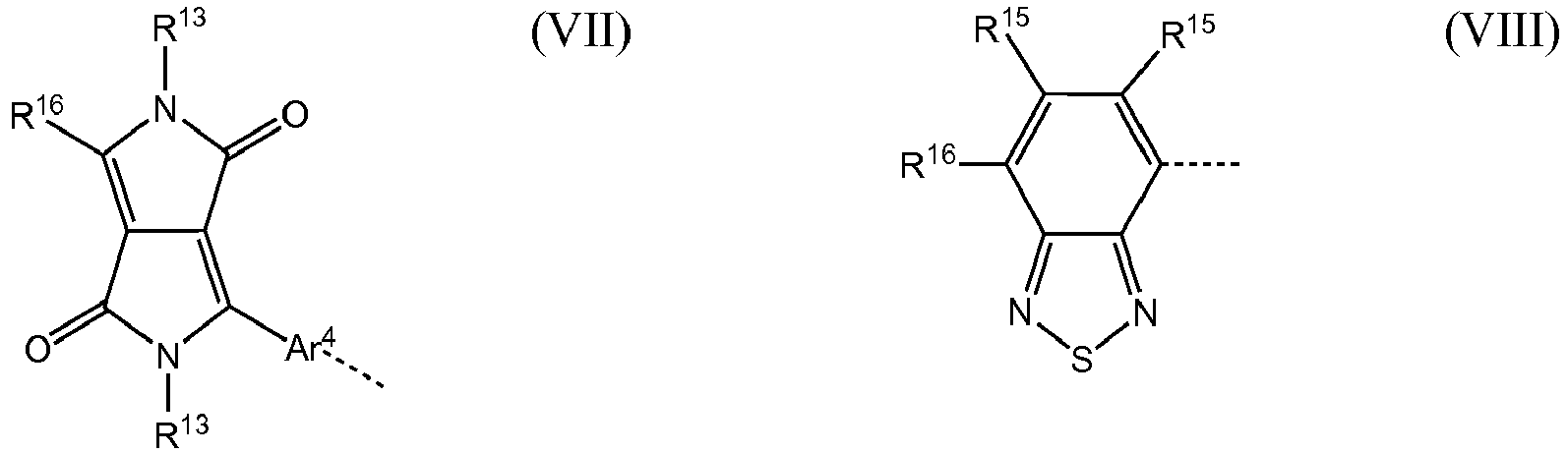


- A is a 5- or 6-membered ring which is unsubstituted or substituted with one or more substituents and which may be fused to one or more further rings.
- R10 is H or a substituent, preferably a substituent selected from the group consisting of C1-12 alkyl wherein one or more non-adjacent, non-terminal C atoms may be replaced with O, S, COO or CO and one or more H atoms of the alkyl may be replaced with F; and an aromatic group Ar2, optionally phenyl, which is unsubstituted or substituted with one or more substituents selected from F and C1-12 alkyl wherein one or more non-adjacent, non-terminal C atoms may be replaced with O, S, COO or CO.
- Preferably, R10 is H.
- J is O or S.
- R13 in each occurrence is a substituent, optionally C1-12 alkyl wherein one or more non-adjacent, non-terminal C atoms may be replaced with O, S, COO or CO and one or more H atoms of the alkyl may be replaced with F.
- R15 in each occurrence is independently H; F; C1-12 alkyl wherein one or more non-adjacent, non-terminal C atoms may be replaced with O, S, COO or CO and one or more H atoms of the alkyl may be replaced with F; or an aromatic group Ar2, optionally phenyl, which is unsubstituted or substituted with one or more substituents selected from F and C1-12 alkyl wherein one or more non-adjacent, non-terminal C atoms may be replaced with O, S, COO or CO.
- R16 is a substituent, preferably a substituent selected from:
- -(Ar3)w wherein Ar3 in each occurrence is independently an unsubstituted or substituted aryl or heteroaryl group, preferably thiophene, and w is 1, 2 or 3;

- C1-12 alkyl wherein one or more non-adjacent, non-terminal C atoms may be replaced with O, S, COO or CO and one or more H atoms of the alkyl may be replaced with F.
- Ar4 is a 5-membered heteroaromatic group, preferably thiophene or furan, which is unsubstituted or substituted with one or more substituents.
- Substituents of Ar3 and Ar4, where present, are optionally selected from C1-12 alkyl wherein one or more non-adjacent, non-terminal C atoms may be replaced with O, S, COO or CO and one or more H atoms of the alkyl may be replaced with F.
- Z1 is N or P
- T1, T2 and T3 each independently represent an aryl or a heteroaryl ring which may be fused to one or more further rings. Substituents of T1, T2 and T3, where present, are optionally selected from non-H groups of R15.
- Ar8 is a fused heteroaromatic group which is unsubstituted or substituted with one or more non-H substituents R10.
- A preferred group of formula (III) is formula (IIIa).
- Preferably at least one, more preferably each, EAG is a group of formula (IIIa):

- R10 is as described above;
- ---- represents a linking position to * of EDG; and
- each X1-X4 is independently CR12 or N wherein R12 in each occurrence is H or a substituent selected from C1-20 hydrocarbyl and an electron withdrawing group. Optionally, the electron withdrawing group is F, Cl, Br or CN.
- The C1-20 hydrocarbyl group R12 may be selected from C1-20 alkyl; unsubstituted phenyl; and phenyl substituted with one or more C1-12 alkyl groups.
- Exemplary compounds of formula (IVa) or (IVb) include:


- Exemplary EAGs of formula (XI) are:

- An exemplary EAG group of formula (XII) is:

- In the case where at least one EAG is a group of formula (XIII), at least one m is 0; at least one of R3 and R6 is -B(R14)2 wherein R14 in each occurrence is a substituent, optionally a C1-20 hydrocarbyl group; → is a bond to the boron atom -B(R14)2 of R3 or R6; and --- is the bond to EDG.
- Optionally, R14 is selected from C1-12 alkyl; unsubstituted phenyl; and phenyl substituted with one or more C1-12 alkyl groups.
- EDG, EAG and the B(R14)2 substituent R3 or R6 of EDG may be linked together to form a 5- or 6-membered ring.
- In some embodiments, EAG of formula (XIII) is selected from formulae (XIIIa), (XIIIb) and (XIIIc):

- Exemplary compounds of formula (I) are:


- The donor (p-type) compound is not particularly limited and may be selected from electron donating materials that are known to the person skilled in the art, including organic polymers and non-polymeric organic molecules. The p-type compound has a HOMO deeper (further from vacuum) than a LUMO of the compound of formula (I). Optionally, the gap between the HOMO level of the p-type donor and the LUMO level of the n-type acceptor compound of formula (I) is less than 1.4 eV.
- In a preferred embodiment the p-type donor compound is an organic conjugated polymer, which can be a homopolymer or copolymer including alternating, random or block copolymers. Preferred are non-crystalline or semi- crystalline conjugated organic polymers. Further preferably the p-type organic semiconductor is a conjugated organic polymer with a low bandgap, typically between 2.5 eV and 1.5 eV, preferably between 2.3 eV and 1.8 eV. As exemplary p-type donor polymers, polymers selected from conjugated hydrocarbon or heterocyclic polymers including polyacene, polyaniline, polyazulene, polybenzofuran, polyfluorene, polyfuran, polyindenofluorene, polyindole, polyphenylene, polypyrazoline, polypyrene, polypyridazine, polypyridine, polytriarylamine, poly(phenylene vinylene), poly(3-substituted thiophene), poly(3,4-bisubstituted thiophene), polyselenophene, poly(3-substituted selenophene), poly(3,4-bisubstituted selenophene), poly(bisthiophene), poly(terthiophene), poly(bisselenophene), poly(terselenophene), polythieno[2,3-b]thiophene, polythieno[3,2-b]thiophene, polybenzothiophene, polybenzo[1,2-b:4,5-b'jdithiophene, polyisothianaphthene, poly(monosubstituted pyrrole), poly(3,4-bisubstituted pyrrole), poly-1 ,3,4-oxadiazoles, polyisothianaphthene, derivatives and co-polymers thereof may be mentioned. Preferred examples of p-type donors are copolymers of polyfluorenes and polythiophenes, each of which may be substituted, and polymers comprising benzothiadiazole-based and thiophene-based repeating units, each of which may be substituted. It is understood that the p-type donor may also consist of a mixture of a plurality of electron donating materials.
- Optionally, the p-type donor has a HOMO level no more than 5.5 eV from vacuum level. Optionally, the p-type donor has a HOMO level at least 4.1 eV from vacuum level.
- Unless stated otherwise, HOMO and LUMO levels of a compound as described herein are as measured from a film of the compound using square wave voltammetry.
- In some embodiments, the weight of the donor compound to the acceptor compound is from about 1:0.5 to about 1:2.
- Preferably, the weight ratio of the donor compound to the acceptor compound is about 1:1 or about 1:1.5.
- At least one of the first and second electrodes is transparent so that light incident on the device may reach the bulk heterojunction layer. In some embodiments, both of the first and second electrodes are transparent.
- Each transparent electrode preferably has a transmittance of at least 70 %, optionally at least 80 %, to wavelengths in the range of 400-750 nm or 750-1000 nm or 1000-2000 nm. The transmittance may be selected according to the absorption peak of the compound of formula (I).
- In some embodiments, one electrode is transparent and the other electrode is reflective.
- Optionally, the transparent electrode comprises or consists of a layer of transparent conducting oxide, preferably indium tin oxide or indium zinc oxide. In preferred embodiments, the electrode may comprise poly 3,4-ethylenedioxythiophene (PEDOT). In other preferred embodiments, the electrode may comprise a mixture of PEDOT and polystyrene sulfonate (PSS). The electrode may consist of a layer of PEDOT:PSS.
- Optionally, the reflective electrode may comprise a layer of a reflective metal. The layer of reflective material may be aluminium or silver or gold. In some embodiments, a bi-layer electrode may be used. For example, the electrode may be an indium tin oxide (ITO)/silver bi-layer, an ITO/aluminium bi-layer or an ITO/gold bi-layer.
- The device may be formed by forming the bulk heterojunction layer over one of the anode and cathode supported by a substrate and depositing the other of the anode or cathode over the bulk heterojunction layer.
- The area of the OPD may be less than about 3 cm2, less than about 2 cm2, less than about 1 cm2, less than about 0.75 cm2, less than about 0.5 cm2 or less than about 0.25 cm2. The substrate may be, without limitation, a glass or plastic substrate. The substrate can be described as an inorganic semiconductor. In some embodiments, the substrate may be silicon. For example, the substrate can be a wafer of silicon. The substrate is transparent if, in use, incident light is to be transmitted through the substrate and the electrode supported by the substrate.
- The substrate supporting one of the anode and cathode may or may not be transparent if, in use, incident light is to be transmitted through the other of the anode and cathode.
- The bulk heterojunction layer may be formed by any process including, without limitation, thermal evaporation and solution deposition methods.
- Preferably, the bulk heterojunction layer is formed by depositing a formulation comprising the acceptor material and the electron donor material dissolved or dispersed in a solvent or a mixture of two or more solvents. The formulation may be deposited by any coating or printing method including, without limitation, spin-coating, dip-coating, roll-coating, spray coating, doctor blade coating, wire bar coating, slit coating, ink jet printing, screen printing, gravure printing and flexographic printing.
- The one or more solvents of the formulation may optionally comprise or consist of benzene substituted with one or more substituents selected from chlorine, C1-10 alkyl and C1-10 alkoxy wherein two or more substituents may be linked to form a ring which may be unsubstituted or substituted with one or more C1-6 alkyl groups, optionally toluene, xylenes, trimethylbenzenes, tetramethylbenzenes, anisole, indane and its alkyl-substituted derivatives, and tetralin and its alkyl-substituted derivatives.
- The formulation may comprise a mixture of two or more solvents, preferably a mixture comprising at least one benzene substituted with one or more substituents as described above and one or more further solvents. The one or more further solvents may be selected from esters, optionally alkyl or aryl esters of alkyl or aryl carboxylic acids, optionally a C1-10 alkyl benzoate, benzyl benzoate or dimethoxybenzene. In preferred embodiments, a mixture of trimethylbenzene and benzyl benzoate is used as the solvent. In other preferred embodiments, a mixture of trimethylbenzene and dimethoxybenzene is used as the solvent.
- The formulation may comprise further components in addition to the electron acceptor, the electron donor and the one or more solvents. As examples of such components, adhesive agents, defoaming agents, deaerators, viscosity enhancers, diluents, auxiliaries, flow improvers colourants, dyes or pigments, sensitizers, stabilizers, nanoparticles, surface-active compounds, lubricating agents, wetting agents, dispersing agents and inhibitors may be mentioned.
- The organic photoresponsive device as described herein may be an organic photovoltaic device or an organic photodetector. An organic photodetector as described herein may be used in a wide range of applications including, without limitation, detecting the presence and / or brightness of ambient light and in a sensor comprising the organic photodetector and a light source. The photodetector may be configured such that light emitted from the light source is incident on the photodetector and changes in wavelength and / or brightness of the light may be detected, e.g. due to absorption by, reflection by and / or emission of light from an object, e.g. a target material in a sample disposed in a light path between the light source and the organic photodetector. The sensor may be, without limitation, a gas sensor, a biosensor, an X-ray imaging device, an image sensor such as a camera image sensor, a motion sensor (for example for use in security applications) a proximity sensor or a fingerprint sensor. A 1D or 2D photosensor array may comprise a plurality of photodetectors as described herein in an image sensor.
- A compound of formula (I) may be prepared according to the following reaction scheme:
-
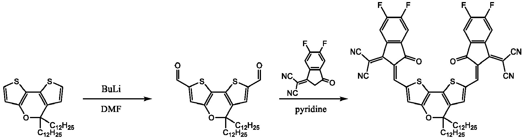
-

-

- LUMO levels of certain electron donating groups of formula (II) were modelled and results are set out in Table 1 in which each bond to an electron-accepting group of formula (I), indicated by a wavy line in Table 1, was replaced with bonds to H.
- LUMO levels of certain electron accepting groups are included for comparison.
- Quantum chemical modelling was performed using Gaussian09 software available from Gaussian using Gaussian09 with B3LYP (functional) and LACVP* (Basis set).
Table 1 Group Structure LUMO /eV EDG 
-1.094 EDG 
-1.758 EAG 
-3.553 EAG 
-2.475 EAG 
-3.379 EAG 
-2.462 EAG 
-2.509 - HOMO and LUMO levels of the following compounds were modelled as described above and results are set out in Table 2.


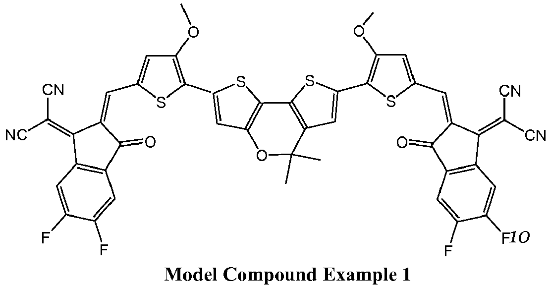
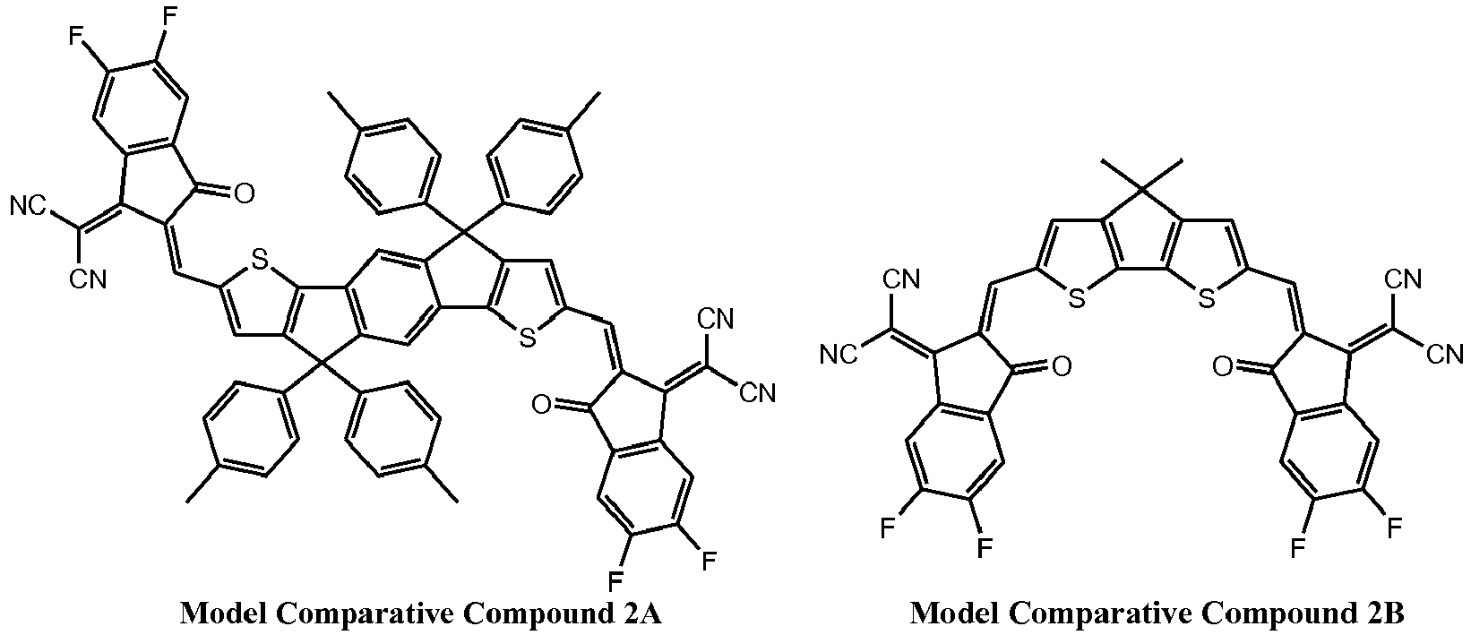


Table 2 Compound HOMO (eV) LUMO (eV) Band gap (eV) Model Comparative Compound 1A -5.147 -3.409 1.738 Model Comparative Compound 1B -5.240 -3.595 1.645 Model Compound Example 1 -5.215 -3.610 1.605 Model Comparative Compound 2A -5.777 -3.566 2.211 Model Comparative Compound 2B -6.092 -3.901 2.191 Model Compound Example 2 -5.989 -3.914 2.074 Model Comparative Compound 3A -4.954 -3.411 1.543 Model Comparative Compound 3B -4.971 -3.433 1.537 Model Compound Example 3 -4.952 -3.468 1.484 - The donor group EDG of Model Compound Example 1 has thiopenes bridging a central fused group and the acceptor (EAG) groups. This compound has a smaller band gap than Model Comparative Compounds 1A and 1B with a different central fused group, indicating that Model Compound Example 1 is capable of absorbing light at longer wavelengths than Model Comparative Compounds 1A and 1B.
- A smaller band gap is also observed for Model Compound Example 2 as compared to Model Comparative Compounds 2A and 2B in which the bridging thiophene groups are not present.
- Model Compound Example 3, in which n of formula (I) is 2, has a smaller band gap than either of Model Compound Examples 1 and 2, and a smaller band gap than either of Model Comparative Compounds 3A and 3B.
Claims (15)
- A composition comprising an electron acceptor material and an electron donor material wherein the electron acceptor material is a compound of formula (I):
EAG-EDG-EAG (I)
wherein each EAG is an electron-accepting group and EDG is a group of formula (II): n is at least 1;each m is independently 0 or at least 1;each X, Y and A is independently O, S or Se;Z, independently in each occurrence if n is greater than 1, is O, S, C=O or NR9 wherein R9 is H or a substituent; andR1 - R8 are each independently selected from H or a substituent.
 - The composition according to claim 1 wherein each EAG is a group of formula (V):
 R10 in each occurrence is H or a substituent selected from the group consisting of: C1-12 alkyl wherein one or more non-adjacent, non-terminal C atoms may be replaced with O, S, COO or CO and one or more H atoms of the alkyl may be replaced with F; and an aromatic group Ar2 which is unsubstituted or substituted with one or more substituents selected from F and C1-12 alkyl wherein one or more non-adjacent, non-terminal C atoms may be replaced with O, S, COO or CO;---- represents a linking position to * of EDG; andeach X1-X4 is independently CR12 or N wherein R12 in each occurrence is H or a substituent selected from C1-20 hydrocarbyl and an electron withdrawing group.
 - The composition according to any one of the preceding claims wherein each m is 0 or 1.
- The composition according to any one of the preceding claims wherein X and Y are each S.
- The composition according to any one of the preceding claims wherein Z is O or NR9.
- The composition according to any one of the preceding claims wherein at least one m is at least 1 and the or each A is S.
- The composition according to any one of the preceding claims wherein R1 - R8 are each independent selected from the group consisting of:H;linear, branched or cyclic C1-20 alkyl wherein one or more non-adjacent, non-terminal C atoms may be replaced by O, S, NR12, CO or COO and wherein one or more H atoms of the C1-20 alkyl may be replaced with F; anda group of formula -(Ak)u-(Ar1)v wherein Ak is a C1-12 alkylene chain in which one or more C atoms may be replaced with O, S, CO or COO; u is 0 or 1; Ar1 in each occurrence is independently an aromatic or heteroaromatic group which is unsubstituted or substituted with one or more substituents; and v is at least 1.
- The composition according to any one of the preceding claims wherein each * is bound directly to an acyclic carbon-carbon double bond of EAG.
- A formulation comprising a composition according to any one of the preceding claims dissolved or dispersed in one or more solvents.
- An organic photoresponsive device comprising an anode; a cathode; and a photosensitive organic layer disposed between the anode and cathode wherein the photosensitive organic layer comprises a composition according to any one of the preceding claims.
- An organic photoresponsive device according to claim 10 wherein the photoresponsive device is an organic photodetector.
- A method of forming an organic photoresponsive device according to claim 10 or 11 comprising formation of the photosensitive organic layer over one of the anode and cathode and formation of the other of the anode and cathode over the photosensitive organic layer wherein formation of the photosensitive organic layer comprises deposition of a formulation comprising composition dissolved or dispersed in one or more solvents.
- A photosensor comprising a light source and an organic photodetector according to claim 11 configured to detect light emitted from the light source.
- A photosensor according to claim 13 wherein the light source emits light having a peak wavelength greater than 750 nm and / or wherein the organic photodetector is configured to detect light emitted from the light source following one or more of absorption, reflection and downconversion of light emitted from the light source.
- A method of determining the presence and / or concentration of a target substance in a sample, the method comprising illuminating the sample and measuring a response of an organic photodetector according to claim 11.
Priority Applications (7)
| Application Number | Priority Date | Filing Date | Title |
|---|---|---|---|
| EP19205205.8A EP3812383A1 (en) | 2019-10-24 | 2019-10-24 | Molecular materials based on phenoxyazine core for heterojunction organic solar cells |
| GBGB2011800.6A GB202011800D0 (en) | 2019-10-24 | 2020-07-29 | Compound |
| PCT/GB2020/052685 WO2021079140A1 (en) | 2019-10-24 | 2020-10-23 | Molecular materials based on phenoxyazine core for heterojunction organic solar cells |
| CN202080071756.9A CN114585627A (en) | 2019-10-24 | 2020-10-23 | Phenoxyazine core-based molecular materials for heterojunction organic solar cells |
| EP20797540.0A EP4048669A1 (en) | 2019-10-24 | 2020-10-23 | Molecular materials based on phenoxyazine core for heterojunction organic solar cells |
| JP2022523703A JP7622053B2 (en) | 2019-10-24 | 2020-10-23 | Phenoxazine core-based molecular materials for heterojunction organic solar cells |
| US17/771,454 US12232415B2 (en) | 2019-10-24 | 2020-10-23 | Molecular materials based on phenoxyazine core for heterojunction organic solar cells |
Applications Claiming Priority (1)
| Application Number | Priority Date | Filing Date | Title |
|---|---|---|---|
| EP19205205.8A EP3812383A1 (en) | 2019-10-24 | 2019-10-24 | Molecular materials based on phenoxyazine core for heterojunction organic solar cells |
Publications (1)
| Publication Number | Publication Date |
|---|---|
| EP3812383A1 true EP3812383A1 (en) | 2021-04-28 |
Family
ID=68344622
Family Applications (2)
| Application Number | Title | Priority Date | Filing Date |
|---|---|---|---|
| EP19205205.8A Withdrawn EP3812383A1 (en) | 2019-10-24 | 2019-10-24 | Molecular materials based on phenoxyazine core for heterojunction organic solar cells |
| EP20797540.0A Pending EP4048669A1 (en) | 2019-10-24 | 2020-10-23 | Molecular materials based on phenoxyazine core for heterojunction organic solar cells |
Family Applications After (1)
| Application Number | Title | Priority Date | Filing Date |
|---|---|---|---|
| EP20797540.0A Pending EP4048669A1 (en) | 2019-10-24 | 2020-10-23 | Molecular materials based on phenoxyazine core for heterojunction organic solar cells |
Country Status (6)
| Country | Link |
|---|---|
| US (1) | US12232415B2 (en) |
| EP (2) | EP3812383A1 (en) |
| JP (1) | JP7622053B2 (en) |
| CN (1) | CN114585627A (en) |
| GB (1) | GB202011800D0 (en) |
| WO (1) | WO2021079140A1 (en) |
Families Citing this family (10)
| Publication number | Priority date | Publication date | Assignee | Title |
|---|---|---|---|---|
| JP7791662B2 (en) * | 2020-07-22 | 2025-12-24 | 住友化学株式会社 | Compound and photoelectric conversion element using the same |
| KR102661218B1 (en) * | 2022-03-07 | 2024-04-25 | 한국화학연구원 | Near-infrared absorbing organic semiconducting material and organic photo detector comprising the same |
| US20240122055A1 (en) * | 2022-09-16 | 2024-04-11 | Raynergy Tek Incorporation | Organic semiconducting compound and organic optoelectronic devices using the same |
| GB2627286A (en) | 2023-02-17 | 2024-08-21 | Sumitomo Chemical Co | Compound |
| GB202302315D0 (en) | 2023-02-17 | 2023-04-05 | Sumitomo Chemical Co | Compound |
| WO2024172105A1 (en) * | 2023-02-17 | 2024-08-22 | 住友化学株式会社 | Compound, composition, ink, photoelectric conversion element, photosensor, and photoelectric conversion material |
| JPWO2024181311A1 (en) | 2023-03-02 | 2024-09-06 | ||
| JPWO2024262486A1 (en) * | 2023-06-22 | 2024-12-26 | ||
| JP2025077474A (en) * | 2023-11-06 | 2025-05-19 | 住友化学株式会社 | Compound, composition, ink, photoelectric conversion element, and optical sensor |
| JP2026019675A (en) * | 2024-07-26 | 2026-02-05 | 住友化学株式会社 | Compound, composition, ink, photoelectric conversion element, and optical sensor |
Citations (3)
| Publication number | Priority date | Publication date | Assignee | Title |
|---|---|---|---|---|
| KR20150114418A (en) * | 2014-03-27 | 2015-10-12 | 주식회사 엘지화학 | Heterocyclic compound and organic solar cell comprising the same |
| EP3064500A2 (en) | 2013-10-28 | 2016-09-07 | LG Chem, Ltd. | Single molecule and organic solar cell comprising same |
| KR20180104398A (en) * | 2017-03-13 | 2018-09-21 | 주식회사 엘지화학 | Heterocyclic compound and organic electronic device comprising the same |
Family Cites Families (11)
| Publication number | Priority date | Publication date | Assignee | Title |
|---|---|---|---|---|
| JP5747789B2 (en) | 2011-07-05 | 2015-07-15 | 住友化学株式会社 | Polymer compound and organic photoelectric conversion device using the same |
| TWI635111B (en) * | 2012-03-16 | 2018-09-11 | Merck Patent Gmbh | Conjugated polymer |
| EP3140872A1 (en) * | 2014-05-07 | 2017-03-15 | SABIC Global Technologies B.V. | Crystallization of additives at p/n junctions of bulk-heterojunction photoactive layers |
| KR101749379B1 (en) * | 2014-06-12 | 2017-06-20 | 주식회사 엘지화학 | Copolymer, manufacturing method the same and organic solar cell comprising the copolymer |
| CN106486558A (en) * | 2015-08-31 | 2017-03-08 | 阿克伦大学 | By the use of quantum dot and perovskite mixture as the photodetector of collection body of light |
| US20170358766A1 (en) * | 2016-06-09 | 2017-12-14 | Solarwindow Technologies, Inc. | Organic semiconductor photovoltaic devices and compositions with acceptor-donor-acceptor type polymer electron donors |
| KR101902129B1 (en) * | 2017-05-24 | 2018-09-28 | 주식회사 엘지화학 | Heterocyclic compound and organic electronic device comprising the same |
| CN109293693B (en) * | 2018-11-19 | 2021-03-30 | 中国科学院重庆绿色智能技术研究院 | A novel dithienosilacyclopentadiene organic solar cell acceptor material and its preparation method and application |
| GB2579416A (en) * | 2018-11-30 | 2020-06-24 | Sumitomo Chemical Co | Photoactive compound |
| CN109776566B (en) * | 2019-01-23 | 2021-12-28 | 深圳大学 | A-D-A conjugated molecule based on multi-substituted benzocyclopentadienone derivative and application thereof |
| GB2602025A (en) * | 2020-12-15 | 2022-06-22 | Sumitomo Chemical Co | Compound |
-
2019
- 2019-10-24 EP EP19205205.8A patent/EP3812383A1/en not_active Withdrawn
-
2020
- 2020-07-29 GB GBGB2011800.6A patent/GB202011800D0/en not_active Ceased
- 2020-10-23 US US17/771,454 patent/US12232415B2/en active Active
- 2020-10-23 JP JP2022523703A patent/JP7622053B2/en active Active
- 2020-10-23 EP EP20797540.0A patent/EP4048669A1/en active Pending
- 2020-10-23 WO PCT/GB2020/052685 patent/WO2021079140A1/en not_active Ceased
- 2020-10-23 CN CN202080071756.9A patent/CN114585627A/en active Pending
Patent Citations (3)
| Publication number | Priority date | Publication date | Assignee | Title |
|---|---|---|---|---|
| EP3064500A2 (en) | 2013-10-28 | 2016-09-07 | LG Chem, Ltd. | Single molecule and organic solar cell comprising same |
| KR20150114418A (en) * | 2014-03-27 | 2015-10-12 | 주식회사 엘지화학 | Heterocyclic compound and organic solar cell comprising the same |
| KR20180104398A (en) * | 2017-03-13 | 2018-09-21 | 주식회사 엘지화학 | Heterocyclic compound and organic electronic device comprising the same |
Non-Patent Citations (2)
| Title |
|---|
| JUNG ET AL.: "A Small Molecule Composed of Dithienopyran and Diketopyrrolopyrrole as Versatile Electron Donor Compatible with Both Fullerene and Nonfullerene Electron Acceptors for High Performance Organic Solar Cells", CHEM. MATER., vol. 27, no. 13, 2015, pages 4865 - 4870 |
| JUNG ET AL.: "A Small Molecule Composed of Dithienopyran and Diketopyrrolopyrrole as Versatile Electron Donor Compatible with Both Fullerene and Nonfullerene Electron Acceptors for High Performance Organic Solar Cells", CHEM. MATER., vol. 27, no. 13, 2015, pages 4865 - 4870, XP002797517 * |
Also Published As
| Publication number | Publication date |
|---|---|
| WO2021079140A1 (en) | 2021-04-29 |
| EP4048669A1 (en) | 2022-08-31 |
| US12232415B2 (en) | 2025-02-18 |
| JP2023500815A (en) | 2023-01-11 |
| US20220407015A1 (en) | 2022-12-22 |
| JP7622053B2 (en) | 2025-01-27 |
| GB202011800D0 (en) | 2020-09-09 |
| CN114585627A (en) | 2022-06-03 |
Similar Documents
| Publication | Publication Date | Title |
|---|---|---|
| EP3812383A1 (en) | Molecular materials based on phenoxyazine core for heterojunction organic solar cells | |
| US20240334825A1 (en) | Photoresponsive nonfullerene acceptors of the a-d-a'-d-a type for use in optoelectronic devices | |
| US12082426B2 (en) | Photodetector composition | |
| US11600785B2 (en) | Photoactive compound | |
| JP2024037774A (en) | organic photodetector | |
| US20210175426A1 (en) | Organic photodetector | |
| US11968885B2 (en) | Organic photodetector | |
| GB2623989A (en) | Compound | |
| WO2021156605A1 (en) | Photoactive material | |
| WO2024115338A1 (en) | Fullerene derivatives in a photoresponsive device | |
| GB2627286A (en) | Compound | |
| US20240196744A1 (en) | Compound | |
| US11043645B2 (en) | Organic photodetector | |
| US20250282793A1 (en) | Compound | |
| US20240206336A1 (en) | Compound | |
| US20240206310A1 (en) | Compound and device | |
| WO2025186103A1 (en) | Compound | |
| WO2024115329A1 (en) | Compounds useful in the preparation of photoresponsive device | |
| WO2022129595A1 (en) | Photoactive material | |
| WO2024170691A1 (en) | Compounds for use in photosensors | |
| WO2024115332A1 (en) | Compounds for organic electronic devices | |
| WO2024115333A1 (en) | Method and compound | |
| JP2026067815A (en) | compound | |
| GB2624704A (en) | Compound | |
| GB2577561A (en) | Method of manufacturing an organic photodetector |
Legal Events
| Date | Code | Title | Description |
|---|---|---|---|
| PUAI | Public reference made under article 153(3) epc to a published international application that has entered the european phase |
Free format text: ORIGINAL CODE: 0009012 |
|
| STAA | Information on the status of an ep patent application or granted ep patent |
Free format text: STATUS: THE APPLICATION HAS BEEN PUBLISHED |
|
| AK | Designated contracting states |
Kind code of ref document: A1 Designated state(s): AL AT BE BG CH CY CZ DE DK EE ES FI FR GB GR HR HU IE IS IT LI LT LU LV MC MK MT NL NO PL PT RO RS SE SI SK SM TR |
|
| AX | Request for extension of the european patent |
Extension state: BA ME |
|
| STAA | Information on the status of an ep patent application or granted ep patent |
Free format text: STATUS: THE APPLICATION IS DEEMED TO BE WITHDRAWN |
|
| 18D | Application deemed to be withdrawn |
Effective date: 20211029 |