EP3809806A1 - Wiring board - Google Patents
Wiring board Download PDFInfo
- Publication number
- EP3809806A1 EP3809806A1 EP20198438.2A EP20198438A EP3809806A1 EP 3809806 A1 EP3809806 A1 EP 3809806A1 EP 20198438 A EP20198438 A EP 20198438A EP 3809806 A1 EP3809806 A1 EP 3809806A1
- Authority
- EP
- European Patent Office
- Prior art keywords
- substrate
- capacitors
- capacitor
- monolithic ceramic
- wiring board
- Prior art date
- Legal status (The legal status is an assumption and is not a legal conclusion. Google has not performed a legal analysis and makes no representation as to the accuracy of the status listed.)
- Granted
Links
Images


Classifications
-
- H—ELECTRICITY
- H05—ELECTRIC TECHNIQUES NOT OTHERWISE PROVIDED FOR
- H05K—PRINTED CIRCUITS; CASINGS OR CONSTRUCTIONAL DETAILS OF ELECTRIC APPARATUS; MANUFACTURE OF ASSEMBLAGES OF ELECTRICAL COMPONENTS
- H05K1/00—Printed circuits
- H05K1/02—Details
- H05K1/11—Printed elements for providing electric connections to or between printed circuits
- H05K1/111—Pads for surface mounting, e.g. lay-out
-
- H—ELECTRICITY
- H05—ELECTRIC TECHNIQUES NOT OTHERWISE PROVIDED FOR
- H05K—PRINTED CIRCUITS; CASINGS OR CONSTRUCTIONAL DETAILS OF ELECTRIC APPARATUS; MANUFACTURE OF ASSEMBLAGES OF ELECTRICAL COMPONENTS
- H05K1/00—Printed circuits
- H05K1/18—Printed circuits structurally associated with non-printed electric components
- H05K1/181—Printed circuits structurally associated with non-printed electric components associated with surface mounted components
-
- H—ELECTRICITY
- H05—ELECTRIC TECHNIQUES NOT OTHERWISE PROVIDED FOR
- H05K—PRINTED CIRCUITS; CASINGS OR CONSTRUCTIONAL DETAILS OF ELECTRIC APPARATUS; MANUFACTURE OF ASSEMBLAGES OF ELECTRICAL COMPONENTS
- H05K1/00—Printed circuits
- H05K1/02—Details
- H05K1/03—Use of materials for the substrate
- H05K1/0313—Organic insulating material
- H05K1/0353—Organic insulating material consisting of two or more materials, e.g. two or more polymers, polymer + filler, + reinforcement
-
- H—ELECTRICITY
- H05—ELECTRIC TECHNIQUES NOT OTHERWISE PROVIDED FOR
- H05K—PRINTED CIRCUITS; CASINGS OR CONSTRUCTIONAL DETAILS OF ELECTRIC APPARATUS; MANUFACTURE OF ASSEMBLAGES OF ELECTRICAL COMPONENTS
- H05K1/00—Printed circuits
- H05K1/02—Details
- H05K1/03—Use of materials for the substrate
- H05K1/0386—Paper sheets
-
- H—ELECTRICITY
- H05—ELECTRIC TECHNIQUES NOT OTHERWISE PROVIDED FOR
- H05K—PRINTED CIRCUITS; CASINGS OR CONSTRUCTIONAL DETAILS OF ELECTRIC APPARATUS; MANUFACTURE OF ASSEMBLAGES OF ELECTRICAL COMPONENTS
- H05K1/00—Printed circuits
- H05K1/02—Details
- H05K1/0213—Electrical arrangements not otherwise provided for
- H05K1/0216—Reduction of cross-talk, noise or electromagnetic interference
- H05K1/023—Reduction of cross-talk, noise or electromagnetic interference using auxiliary mounted passive components or auxiliary substances
- H05K1/0231—Capacitors or dielectric substances
-
- H—ELECTRICITY
- H05—ELECTRIC TECHNIQUES NOT OTHERWISE PROVIDED FOR
- H05K—PRINTED CIRCUITS; CASINGS OR CONSTRUCTIONAL DETAILS OF ELECTRIC APPARATUS; MANUFACTURE OF ASSEMBLAGES OF ELECTRICAL COMPONENTS
- H05K1/00—Printed circuits
- H05K1/02—Details
- H05K1/0271—Arrangements for reducing stress or warp in rigid printed circuit boards, e.g. caused by loads, vibrations or differences in thermal expansion
-
- H—ELECTRICITY
- H05—ELECTRIC TECHNIQUES NOT OTHERWISE PROVIDED FOR
- H05K—PRINTED CIRCUITS; CASINGS OR CONSTRUCTIONAL DETAILS OF ELECTRIC APPARATUS; MANUFACTURE OF ASSEMBLAGES OF ELECTRICAL COMPONENTS
- H05K2201/00—Indexing scheme relating to printed circuits covered by H05K1/00
- H05K2201/09—Shape and layout
- H05K2201/09209—Shape and layout details of conductors
- H05K2201/09218—Conductive traces
- H05K2201/09227—Layout details of a plurality of traces, e.g. escape layout for Ball Grid Array [BGA] mounting
-
- H—ELECTRICITY
- H05—ELECTRIC TECHNIQUES NOT OTHERWISE PROVIDED FOR
- H05K—PRINTED CIRCUITS; CASINGS OR CONSTRUCTIONAL DETAILS OF ELECTRIC APPARATUS; MANUFACTURE OF ASSEMBLAGES OF ELECTRICAL COMPONENTS
- H05K2201/00—Indexing scheme relating to printed circuits covered by H05K1/00
- H05K2201/09—Shape and layout
- H05K2201/09209—Shape and layout details of conductors
- H05K2201/09218—Conductive traces
- H05K2201/09272—Layout details of angles or corners
-
- H—ELECTRICITY
- H05—ELECTRIC TECHNIQUES NOT OTHERWISE PROVIDED FOR
- H05K—PRINTED CIRCUITS; CASINGS OR CONSTRUCTIONAL DETAILS OF ELECTRIC APPARATUS; MANUFACTURE OF ASSEMBLAGES OF ELECTRICAL COMPONENTS
- H05K2201/00—Indexing scheme relating to printed circuits covered by H05K1/00
- H05K2201/09—Shape and layout
- H05K2201/09209—Shape and layout details of conductors
- H05K2201/09372—Pads and lands
- H05K2201/09418—Special orientation of pads, lands or terminals of component, e.g. radial or polygonal orientation
-
- H—ELECTRICITY
- H05—ELECTRIC TECHNIQUES NOT OTHERWISE PROVIDED FOR
- H05K—PRINTED CIRCUITS; CASINGS OR CONSTRUCTIONAL DETAILS OF ELECTRIC APPARATUS; MANUFACTURE OF ASSEMBLAGES OF ELECTRICAL COMPONENTS
- H05K2201/00—Indexing scheme relating to printed circuits covered by H05K1/00
- H05K2201/10—Details of components or other objects attached to or integrated in a printed circuit board
- H05K2201/10007—Types of components
- H05K2201/10015—Non-printed capacitor
-
- H—ELECTRICITY
- H05—ELECTRIC TECHNIQUES NOT OTHERWISE PROVIDED FOR
- H05K—PRINTED CIRCUITS; CASINGS OR CONSTRUCTIONAL DETAILS OF ELECTRIC APPARATUS; MANUFACTURE OF ASSEMBLAGES OF ELECTRICAL COMPONENTS
- H05K2201/00—Indexing scheme relating to printed circuits covered by H05K1/00
- H05K2201/10—Details of components or other objects attached to or integrated in a printed circuit board
- H05K2201/10613—Details of electrical connections of non-printed components, e.g. special leads
- H05K2201/10621—Components characterised by their electrical contacts
- H05K2201/10636—Leadless chip, e.g. chip capacitor or resistor
-
- Y—GENERAL TAGGING OF NEW TECHNOLOGICAL DEVELOPMENTS; GENERAL TAGGING OF CROSS-SECTIONAL TECHNOLOGIES SPANNING OVER SEVERAL SECTIONS OF THE IPC; TECHNICAL SUBJECTS COVERED BY FORMER USPC CROSS-REFERENCE ART COLLECTIONS [XRACs] AND DIGESTS
- Y02—TECHNOLOGIES OR APPLICATIONS FOR MITIGATION OR ADAPTATION AGAINST CLIMATE CHANGE
- Y02P—CLIMATE CHANGE MITIGATION TECHNOLOGIES IN THE PRODUCTION OR PROCESSING OF GOODS
- Y02P70/00—Climate change mitigation technologies in the production process for final industrial or consumer products
- Y02P70/50—Manufacturing or production processes characterised by the final manufactured product
Definitions
- a capacitor is one of electronic components mounted on a wiring board.
- Examples of capacitors include ceramic capacitors, tantalum capacitors, and aluminum electrolytic capacitors. Since a plurality of capacitors are usually used on one wiring board, various ingenuities have been tried for the arrangement of the capacitors.
- a proposed technique to alleviate the noise is changing arrangement angles of a plurality of monolithic ceramic capacitors to reduce the vibration of the monolithic ceramic capacitors (for example, JP-2010-45085-A ).
- a monolithic ceramic capacitor is a capacitor type in which a crack causes a short circuit. For example, when stress is applied to the wiring board mounted with the monolithic ceramic capacitor, the stress may cause a crack in the monolithic ceramic capacitor, resulting in short circuit.
- a monolithic ceramic capacitor when a monolithic ceramic capacitor is connected between different DC potentials, such as a power supply potential and a ground potential, upon a short circuit, a large current may flow between the different DC potentials.
- DC potentials such as a power supply potential and a ground potential
- a technique being considered is connecting a plurality of monolithic ceramic capacitors in series between the different DC potentials. In such an arrangement, even when a short circuit occurs in one of the monolithic ceramic capacitors, insulation will be maintained by other serially connected monolithic ceramic capacitors, and flowing of a large current between the different DC potentials can be prevented.
- the plurality of monolithic ceramic capacitors connected in series is usually mounted at a short distance from each other on the wiring board. Therefore, when stress is applied to the wiring board, the same stress is applied to each monolithic ceramic capacitor, and all the monolithic ceramic capacitors may be cracked. In this case, if a short circuit due to the crack occurs in all the monolithic ceramic capacitors, a large current flows between the different DC potentials. However, this problem is not solved by the capacitor arrangement proposed in JP-2010-45085-A .
- an object of the present disclosure is to prevent a simultaneous occurrence of a short circuit in each monolithic ceramic capacitor on a wiring board mounted with a plurality of monolithic ceramic capacitors connected in series.
- the wiring board includes a substrate and a plurality of monolithic ceramic capacitors connected in series on the substrate.
- the plurality of monolithic ceramic capacitors includes a first monolithic ceramic capacitor oriented in a first direction and a second monolithic ceramic capacitor oriented in a second direction.
- the second direction is at an angle of 45 ⁇ 5 degrees relative to the first direction.
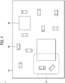
- FIG. 1 is a plan view illustrating a wiring board according to the present embodiment.
- a wiring board 1 includes a substrate 10, an active component 20, and a passive component 30.
- the active component 20 and the passive component 30 are mounted on one side of the substrate 10. However, another active component 20 and another passive component 30 can be mounted also on the other side of the substrate 10 as double-sided mounting.
- Terminals of the active component 20 and the passive component 30 are connected to a component mounting land on the substrate 10 by soldering or the like.
- the substrate 10 is mounted with a wiring pattern for connecting together required portions of the terminals of the active component 20 and the passive component 30, a power supply wiring (VDD wiring) pattern connected to the active component 20, and a ground wiring (GND wiring) pattern.
- VDD wiring power supply wiring
- GND wiring ground wiring
- the substrate 10 is not particularly limited, but is, for example, a resin substrate (a glass epoxy substrate, a phenolic paper substrate, etc.), a ceramic substrate, a silicon substrate, or the like.
- the substrate 10 can be any one of a single-sided substrate having a wiring pattern on one side, a double-sided substrate having wiring patterns on both sides, and a multi-layer substrate in which a plurality of wiring patterns are laminated via insulation layers.
- the active component 20 is not particularly limited, but is, for example, a semiconductor integrated circuit, a transistor, a diode, or the like.
- the passive component 30 is not particularly limited, but is, for example, a capacitor, a resistor, an inductor, a connector, or the like.
- FIG. 2 is an enlarged view of a portion A in FIG. 1 and illustrates an arrangement of capacitors according to the present embodiment.
- FIG. 3 is a circuit diagram corresponding to FIG. 2 .
- supply voltage (VDD) wiring H1 having a power supply potential and ground (GND) wiring H2 having a ground potential are connected to an integrated circuit (IC) IC1.
- IC integrated circuit
- capacitors C1 and C2 also collectively “capacitors C", which are bypass capacitors, are connected in series.
- the IC IC1 is a semiconductor integrated circuit, and the capacitors C1 and C2 are monolithic ceramic capacitors.
- the IC IC1 is a part of the active component 20 illustrated in FIG. 1 .
- the capacitors C1 and C2 are a part of the passive component 30 illustrated in FIG. 1 .
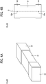
- FIGS. 4A and 4B are views illustrating an external appearance of each of the capacitors.
- FIG. 4A is a perspective view
- FIG. 4B is a plan view.
- each of the capacitors C1 and C2 has a substantially rectangular parallelepiped body 31, and electrodes 32 and 33 on opposite sides of the body 31 from each other.
- the body 31 is, for example, a dielectric made of barium titanate or the like.
- the electrodes 32 and 33 are electric conductors and are made of, for example, copper plated with tin.
- FIG. 4B in a plan view, a direction indicated by a broken line D in FIG. 4B , in which a center 32a of the electrode 32 is connected with a center 33a of the electrode 33, is referred to as a mounting direction D of the capacitor C1 or C2.
- the broken line D1 indicates the mounting direction of the capacitor C1, that is, an orientation of the capacitor C1 on the substrate 10 (hereinafter also “mounting direction D1"). In other words, the capacitor C1 is mounted in the direction indicated by the broken line D1 on the substrate 10.
- a broken line D2 indicates the mounting direction of the capacitor C2 on the substrate 10 (hereinafter also “mounting direction D2"). In other words, the capacitor C2 is mounted in the direction indicated by the broken line D2 on the substrate 10.
- an angle ⁇ between the mounting direction D1 and the mounting direction D2 is 45 ⁇ 5 degrees.
- a component mounted on the wiring board 1 may be cracked, resulting in a short circuit.
- a short circuit may occur between the supply voltage and the ground, and a large current may flow.
- capacitor refers to a monolithic ceramic capacitor.
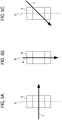
- the possibility of occurrence of a crack is relatively low in a case where the angle of a stress F is 90 degrees (perpendicular) to the mounting direction D of the capacitor C as illustrated in FIG. 5A and a case where the angle of the stress F is 0 degree (parallel) to the mounting direction D of the capacitor C as illustrated in FIG. 5B .
- each of the capacitors C1 and C2 receives the stress F at an angle ⁇ 1 or ⁇ 2 of about 45 degrees relative to the mounting directions D1 and D2.
- the capacitors C1 and C2 may be cracked, resulting a short circuit. There is a risk that a short circuit occurs between the supply voltage and the ground, and a large current flows.
- the mounting direction D1 of the capacitor C1 is deviated by the angle ⁇ of 45 degrees from the mounting direction D2 of the capacitor C2.
- the angle ⁇ 2 relative to the mounting direction D2, of the stress applied to the capacitor C2 is 90 degrees.
- the angle ⁇ 2 is 0 degrees or 90 degrees, the possibility of the occurrence of a crack by the same stress F is low.
- this arrangement can reduce the risk of the short circuit between the supply voltage and the ground and a flow of large current.
- the angle ⁇ between the mounting direction D1 and the mounting direction D2 is 45 ⁇ 5 degrees, the above effect can be obtained to the same extent as in the case where the angle ⁇ is 45 degrees.
- the capacitor C1 is mounted in the mounting direction D1 (oriented in a first direction), and the capacitor C2 is mounted in the mounting direction D2 (oriented in a second direction) that is at an angle of 45 ⁇ 5 degrees relative to the mounting direction D1.
- the direction (relative to the mounting direction) of the applied stress differs between the capacitors C1 and C2.
- This arrangement can prevent application of stress in the same direction to each of the capacitors and prevent a resultant crack in each of the capacitors to cause a short circuit.
- the stress occurs, for example, when another connector is inserted into or removed from the connector mounted on the substrate 10.
- a stress may occur when an operator pushes the wiring board 1 with a finger during the manufacturing of the wiring board 1 or after the wiring board 1 is manufactured.
- the stress generated at this time is more easily transmitted to the capacitors C1 and C2 as the rigidity of the substrate used decreases. Therefore, the lower the rigidity of the substrate 10 is, the greater the technical significance of setting the angle between the mounting directions D1 and D2 to 45 ⁇ 5 degrees, to prevent the occurrence of cracks in the capacitors C1 and C2.
- the technical significance of setting the angle between the mounting direction D1 and the mounting direction D2 to 45 ⁇ 5 degrees and preventing the occurrence of cracks in the capacitors C1 and C2 is greater in a case where a resin substrate is used for the substrate 10, compared with a case where a ceramic substrate or a silicon substrate is used.
- a greater technical significance is attained by setting the angle between the mounting directions D1 and D2 to 45 ⁇ 5 degrees, to prevent the occurrence of cracks in the capacitors C1 and C2.
- the different DC potentials are not limited to the power supply potential and the ground potential.
- the different DC potentials can be a potential divided from the power supply potential and the ground potential.
- the capacitor arrangement according to the present embodiment can be applied to both between the positive power supply potential and the ground potential and between the negative power supply potential and the ground potential.
- the capacitor arrangement according to the present embodiment is applicable to, not only to the capacitors between different DC potentials, a plurality of capacitors connected in series between any two wires, regardless of DC or AC.
- the capacitor arrangement described above can prevent the inconvenience that all capacitors are cracked and a short circuit in each capacitor occurs at the same time, causing a short circuit between the wires.
Landscapes
- Engineering & Computer Science (AREA)
- Microelectronics & Electronic Packaging (AREA)
- Structures For Mounting Electric Components On Printed Circuit Boards (AREA)
Abstract
Description
- A capacitor is one of electronic components mounted on a wiring board. Examples of capacitors include ceramic capacitors, tantalum capacitors, and aluminum electrolytic capacitors. Since a plurality of capacitors are usually used on one wiring board, various ingenuities have been tried for the arrangement of the capacitors.
- For example, when an audio-frequency range voltage superimposed on a direct current (DC) voltage is applied to a monolithic ceramic capacitor used in a switching circuit, an inverse piezoelectric effect corresponding to an alternating current (AC) component of the electric field occurs. Then, a body of the monolithic ceramic capacitor resonates at a natural frequency thereof and vibrates, and the vibration may be transmitted to the board, causing noise. A proposed technique to alleviate the noise is changing arrangement angles of a plurality of monolithic ceramic capacitors to reduce the vibration of the monolithic ceramic capacitors (for example,
JP-2010-45085-A - A monolithic ceramic capacitor is a capacitor type in which a crack causes a short circuit. For example, when stress is applied to the wiring board mounted with the monolithic ceramic capacitor, the stress may cause a crack in the monolithic ceramic capacitor, resulting in short circuit.
- For example, when a monolithic ceramic capacitor is connected between different DC potentials, such as a power supply potential and a ground potential, upon a short circuit, a large current may flow between the different DC potentials.
- Therefore, a technique being considered is connecting a plurality of monolithic ceramic capacitors in series between the different DC potentials. In such an arrangement, even when a short circuit occurs in one of the monolithic ceramic capacitors, insulation will be maintained by other serially connected monolithic ceramic capacitors, and flowing of a large current between the different DC potentials can be prevented.
- However, the plurality of monolithic ceramic capacitors connected in series is usually mounted at a short distance from each other on the wiring board. Therefore, when stress is applied to the wiring board, the same stress is applied to each monolithic ceramic capacitor, and all the monolithic ceramic capacitors may be cracked. In this case, if a short circuit due to the crack occurs in all the monolithic ceramic capacitors, a large current flows between the different DC potentials. However, this problem is not solved by the capacitor arrangement proposed in
JP-2010-45085-A - In view of the foregoing, an object of the present disclosure is to prevent a simultaneous occurrence of a short circuit in each monolithic ceramic capacitor on a wiring board mounted with a plurality of monolithic ceramic capacitors connected in series.
- In order to achieve the above-described object, there is provided a wiring board as described in appended claims. Advantageous embodiments are defined by the dependent claims.
- Advantageously, the wiring board includes a substrate and a plurality of monolithic ceramic capacitors connected in series on the substrate. The plurality of monolithic ceramic capacitors includes a first monolithic ceramic capacitor oriented in a first direction and a second monolithic ceramic capacitor oriented in a second direction. The second direction is at an angle of 45±5 degrees relative to the first direction.
- Accordingly, on a wiring board mounted with a plurality of monolithic ceramic capacitors connected in series, a simultaneous occurrence of a short circuit in each monolithic ceramic capacitor can be prevented.
- A more complete appreciation of the disclosure and many of the attendant advantages thereof will be readily obtained as the same becomes better understood by reference to the following detailed description when considered in connection with the accompanying drawings, wherein:
-
FIG. 1 is a plan view illustrating a wiring board according to an embodiment of the present disclosure; -
FIG. 2 is an enlarged view of a portion of the wiring board inFIG. 1 ; -
FIG. 3 is a circuit diagram corresponding toFIG. 2 ; -
FIGS. 4A and 4B are views illustrating an appearance of a capacitor; -
FIGS. 5A, 5B, and 5C illustrate relationships between a direction of stress and the possibility of occurrence of a crack in a capacitor; and -
FIGS. 6A to 6D illustrate an effect of a capacitor arrangement according to an embodiment of the present disclosure. - The accompanying drawings are intended to depict embodiments of the present invention and should not be interpreted to limit the scope thereof. The accompanying drawings are not to be considered as drawn to scale unless explicitly noted.
- In describing embodiments illustrated in the drawings, specific terminology is employed for the sake of clarity. However, the disclosure of this patent specification is not intended to be limited to the specific terminology so selected, and it is to be understood that each specific element includes all technical equivalents that operate in a similar manner and achieve a similar result.
- Referring now to the drawings, wherein like reference numerals designate identical or corresponding parts throughout the several views thereof, embodiments according to the present disclosure are described. As used herein, the singular forms "a," "an," and "the" are
FIG. 1 is a plan view illustrating a wiring board according to the present embodiment. - Referring to
FIG. 1 , awiring board 1 includes asubstrate 10, anactive component 20, and apassive component 30. - The
active component 20 and thepassive component 30 are mounted on one side of thesubstrate 10. However, anotheractive component 20 and anotherpassive component 30 can be mounted also on the other side of thesubstrate 10 as double-sided mounting. - Terminals of the
active component 20 and thepassive component 30 are connected to a component mounting land on thesubstrate 10 by soldering or the like. Thesubstrate 10 is mounted with a wiring pattern for connecting together required portions of the terminals of theactive component 20 and thepassive component 30, a power supply wiring (VDD wiring) pattern connected to theactive component 20, and a ground wiring (GND wiring) pattern. - The
substrate 10 is not particularly limited, but is, for example, a resin substrate (a glass epoxy substrate, a phenolic paper substrate, etc.), a ceramic substrate, a silicon substrate, or the like. Thesubstrate 10 can be any one of a single-sided substrate having a wiring pattern on one side, a double-sided substrate having wiring patterns on both sides, and a multi-layer substrate in which a plurality of wiring patterns are laminated via insulation layers. - The
active component 20 is not particularly limited, but is, for example, a semiconductor integrated circuit, a transistor, a diode, or the like. Thepassive component 30 is not particularly limited, but is, for example, a capacitor, a resistor, an inductor, a connector, or the like. -
FIG. 2 is an enlarged view of a portion A inFIG. 1 and illustrates an arrangement of capacitors according to the present embodiment.FIG. 3 is a circuit diagram corresponding toFIG. 2 . Referring toFIGS. 2 and 3 , supply voltage (VDD) wiring H1 having a power supply potential and ground (GND) wiring H2 having a ground potential are connected to an integrated circuit (IC) IC1. Between the supply voltage wiring H1 and the ground wiring H2, capacitors C1 and C2 (also collectively "capacitors C"), which are bypass capacitors, are connected in series. - The IC IC1 is a semiconductor integrated circuit, and the capacitors C1 and C2 are monolithic ceramic capacitors. The IC IC1 is a part of the
active component 20 illustrated inFIG. 1 . The capacitors C1 and C2 are a part of thepassive component 30 illustrated inFIG. 1 . -
FIGS. 4A and 4B are views illustrating an external appearance of each of the capacitors.FIG. 4A is a perspective view, andFIG. 4B is a plan view. As illustrated inFIGS. 4A and 4B , each of the capacitors C1 and C2 has a substantially rectangularparallelepiped body 31, andelectrodes body 31 from each other. Thebody 31 is, for example, a dielectric made of barium titanate or the like. Theelectrodes - In the present embodiment, as illustrated in
FIG. 4B , in a plan view, a direction indicated by a broken line D inFIG. 4B , in which acenter 32a of theelectrode 32 is connected with acenter 33a of theelectrode 33, is referred to as a mounting direction D of the capacitor C1 or C2. - Returning to the description of
FIG. 2 , the broken line D1 indicates the mounting direction of the capacitor C1, that is, an orientation of the capacitor C1 on the substrate 10 (hereinafter also "mounting direction D1"). In other words, the capacitor C1 is mounted in the direction indicated by the broken line D1 on thesubstrate 10. A broken line D2 indicates the mounting direction of the capacitor C2 on the substrate 10 (hereinafter also "mounting direction D2"). In other words, the capacitor C2 is mounted in the direction indicated by the broken line D2 on thesubstrate 10. In the capacitor arrangement illustrated inFIG. 2 , an angle θ between the mounting direction D1 and the mounting direction D2 is 45±5 degrees. An advantage thereof is described below. - It is possible that various stresses are applied to the
wiring board 1. Depending on the direction of the stress, a component mounted on thewiring board 1 may be cracked, resulting in a short circuit. For example, when a short circuit occurs in the capacitors C1 and C2 in the circuit illustrated inFIG. 3 , a short circuit may occur between the supply voltage and the ground, and a large current may flow. - Therefore, the inventors have studied the relationship between the direction in which stress is applied to a monolithic ceramic capacitor and the possibility of occurrence of a crack in the monolithic ceramic capacitor. Hereinafter, unless otherwise specified, the term "capacitor" refers to a monolithic ceramic capacitor.
- According to the studies by the inventors, the possibility of occurrence of a crack is relatively low in a case where the angle of a stress F is 90 degrees (perpendicular) to the mounting direction D of the capacitor C as illustrated in
FIG. 5A and a case where the angle of the stress F is 0 degree (parallel) to the mounting direction D of the capacitor C as illustrated inFIG. 5B . - By contrast, when the angle of the stress F is 45 degrees to the mounting direction D of the capacitor C as illustrated in
FIG. 5C , the possibility of occurrence of a crack is higher compared with the cases illustrated inFIGS. 5A and 5B . - From this result, as illustrated in
FIG. 6A , in the arrangement in which the mounting directions D1 and D2 of the capacitors C1 and C2 are the same, it is possible that each of the capacitors C1 and C2 receives the stress F at an angle α1 or α2 of about 45 degrees relative to the mounting directions D1 and D2. In this case, as illustrated inFIG. 6B , the capacitors C1 and C2 may be cracked, resulting a short circuit. There is a risk that a short circuit occurs between the supply voltage and the ground, and a large current flows. - On the other hand, in
FIG. 6C , the mounting direction D1 of the capacitor C1 is deviated by the angle θ of 45 degrees from the mounting direction D2 of the capacitor C2. In this arrangement, when a stress at the angle α1 of 45 degrees relative to the mounting direction D1 is applied to the capacitor C1, the angle α2, relative to the mounting direction D2, of the stress applied to the capacitor C2 is 90 degrees. As described above with reference toFIGS. 5A to 5C , when the angle α2 is 0 degrees or 90 degrees, the possibility of the occurrence of a crack by the same stress F is low. As a result, even when the capacitor C1 is cracked and a short circuit occurs, the capacitor C2 is not cracked and continues to operate normally as illustrated inFIG. 6D . Therefore, this arrangement can reduce the risk of the short circuit between the supply voltage and the ground and a flow of large current. - According to the consideration made by the inventors, when the angle θ between the mounting direction D1 and the mounting direction D2 is 45±5 degrees, the above effect can be obtained to the same extent as in the case where the angle θ is 45 degrees.
- As described above, in the capacitor arrangement according to the present embodiment, the capacitor C1 is mounted in the mounting direction D1 (oriented in a first direction), and the capacitor C2 is mounted in the mounting direction D2 (oriented in a second direction) that is at an angle of 45±5 degrees relative to the mounting direction D1.
- With this arrangement, the direction (relative to the mounting direction) of the applied stress differs between the capacitors C1 and C2. This arrangement can prevent application of stress in the same direction to each of the capacitors and prevent a resultant crack in each of the capacitors to cause a short circuit.
- The stress occurs, for example, when another connector is inserted into or removed from the connector mounted on the
substrate 10. Alternatively, a stress may occur when an operator pushes thewiring board 1 with a finger during the manufacturing of thewiring board 1 or after thewiring board 1 is manufactured. - The stress generated at this time is more easily transmitted to the capacitors C1 and C2 as the rigidity of the substrate used decreases. Therefore, the lower the rigidity of the
substrate 10 is, the greater the technical significance of setting the angle between the mounting directions D1 and D2 to 45±5 degrees, to prevent the occurrence of cracks in the capacitors C1 and C2. - That is, the technical significance of setting the angle between the mounting direction D1 and the mounting direction D2 to 45±5 degrees and preventing the occurrence of cracks in the capacitors C1 and C2 is greater in a case where a resin substrate is used for the
substrate 10, compared with a case where a ceramic substrate or a silicon substrate is used. In particular, when a phenolic paper substrate having a low rigidity among resin substrates is used as thesubstrate 10, a greater technical significance is attained by setting the angle between the mounting directions D1 and D2 to 45±5 degrees, to prevent the occurrence of cracks in the capacitors C1 and C2. - The above description concerns the example where two capacitors are connected in series between different DC potentials. However, even when three or more capacitors are connected in series between different DC potentials, the same effect as above can be obtained by shifting the mounting direction of at least two capacitors by 45±5 degrees.
- Further, the different DC potentials are not limited to the power supply potential and the ground potential. For example, the different DC potentials can be a potential divided from the power supply potential and the ground potential. Further, when there is a positive power supply potential and a negative power supply potential relative to the ground potential, the capacitor arrangement according to the present embodiment can be applied to both between the positive power supply potential and the ground potential and between the negative power supply potential and the ground potential.
- Further, the capacitor arrangement according to the present embodiment is applicable to, not only to the capacitors between different DC potentials, a plurality of capacitors connected in series between any two wires, regardless of DC or AC. In this case, the capacitor arrangement described above can prevent the inconvenience that all capacitors are cracked and a short circuit in each capacitor occurs at the same time, causing a short circuit between the wires.
- The above-described embodiments are illustrative and do not limit the present disclosure. Thus, numerous additional modifications and variations are possible in light of the above teachings. For example, elements and/or features of different illustrative embodiments may be combined with each other and/or substituted for each other within the scope of the present disclosure.
Claims (5)
- A wiring board (1) comprising:a substrate (10);a plurality of monolithic ceramic capacitors (C1,C2) connected in series on the substrate (10) and including:a first monolithic ceramic capacitor (C1) oriented in a first direction; anda second monolithic ceramic capacitor (C2) oriented in a second direction at an angle of 45±5 degrees relative to the first direction.
- The wiring board (1) according to claim 1,
wherein the plurality of monolithic ceramic capacitors (C1,C2) is connected in series between two different direct current potentials. - The wiring board (1) according to claim 2,
further comprising a semiconductor integrated circuit (IC1) mounted on the substrate (10),
wherein one of the different direct current potentials is a power supply potential connected to the semiconductor integrated circuit (IC1), and the other of the different direct current potentials is a ground potential connected to the semiconductor integrated circuit (IC1). - The wiring board (1) according to any one of claims 1 to 3,
wherein the substrate (10) is a resin substrate (10). - The wiring board (1) according to claim 4,
wherein the substrate (10) is a phenolic paper substrate (10).
Applications Claiming Priority (1)
| Application Number | Priority Date | Filing Date | Title |
|---|---|---|---|
| JP2019191343A JP2021068757A (en) | 2019-10-18 | 2019-10-18 | Wiring board |
Publications (2)
| Publication Number | Publication Date |
|---|---|
| EP3809806A1 true EP3809806A1 (en) | 2021-04-21 |
| EP3809806B1 EP3809806B1 (en) | 2026-03-04 |
Family
ID=72659659
Family Applications (1)
| Application Number | Title | Priority Date | Filing Date |
|---|---|---|---|
| EP20198438.2A Active EP3809806B1 (en) | 2019-10-18 | 2020-09-25 | Wiring board |
Country Status (4)
| Country | Link |
|---|---|
| US (1) | US11490518B2 (en) |
| EP (1) | EP3809806B1 (en) |
| JP (1) | JP2021068757A (en) |
| CN (1) | CN112689387A (en) |
Families Citing this family (3)
| Publication number | Priority date | Publication date | Assignee | Title |
|---|---|---|---|---|
| JP7226303B2 (en) * | 2019-12-26 | 2023-02-21 | 株式会社デンソー | Control device |
| CN114142452A (en) * | 2021-11-15 | 2022-03-04 | 中汽创智科技有限公司 | Power supply circuit and vehicle |
| WO2024224912A1 (en) * | 2023-04-27 | 2024-10-31 | 株式会社村田製作所 | Mounting substrate and mounting structure |
Citations (3)
| Publication number | Priority date | Publication date | Assignee | Title |
|---|---|---|---|---|
| US6992374B1 (en) * | 2004-06-14 | 2006-01-31 | Cisco Technology, Inc. | Techniques for manufacturing a circuit board with an improved layout for decoupling capacitors |
| JP2010045085A (en) | 2008-08-11 | 2010-02-25 | Lenovo Singapore Pte Ltd | Arrangement structure in printed circuit board for stacked ceramic capacitor |
| JP2014207531A (en) * | 2013-04-11 | 2014-10-30 | 三菱電機株式会社 | Power supply circuit for high-frequency noise countermeasure |
Family Cites Families (16)
| Publication number | Priority date | Publication date | Assignee | Title |
|---|---|---|---|---|
| JP4026267B2 (en) * | 1998-04-07 | 2007-12-26 | 株式会社デンソー | Electronic component mounting structure and mounting method |
| US6664714B2 (en) * | 2000-03-23 | 2003-12-16 | Elliptec Resonant Actuator Ag | Vibratory motors and methods of making and using same |
| JP4189923B2 (en) * | 2004-06-25 | 2008-12-03 | 株式会社リコー | Image forming method, image forming apparatus using the same, and process cartridge |
| JP2006032377A (en) * | 2004-07-12 | 2006-02-02 | Shizuki Electric Co Inc | Dry capacitor |
| JP2007123309A (en) * | 2005-10-25 | 2007-05-17 | Matsushita Electric Ind Co Ltd | Digital signal processing board |
| US7932471B2 (en) * | 2005-08-05 | 2011-04-26 | Ngk Spark Plug Co., Ltd. | Capacitor for incorporation in wiring board, wiring board, method of manufacturing wiring board, and ceramic chip for embedment |
| JP4724147B2 (en) | 2007-04-26 | 2011-07-13 | レノボ・シンガポール・プライベート・リミテッド | Multilayer ceramic capacitor and its mounting structure |
| JP2009032821A (en) * | 2007-07-25 | 2009-02-12 | Denso Corp | Two-terminal element mounting structure |
| JP5536682B2 (en) * | 2011-01-18 | 2014-07-02 | 日本特殊陶業株式会社 | Component built-in wiring board |
| JP6342994B2 (en) * | 2014-04-24 | 2018-06-13 | ルネサスエレクトロニクス株式会社 | Semiconductor device and manufacturing method thereof |
| US10306755B2 (en) * | 2014-12-08 | 2019-05-28 | Fujikura Ltd. | Stretchable board |
| KR101858709B1 (en) * | 2016-08-05 | 2018-05-16 | 동우 화인켐 주식회사 | Touch sensor laminate, touch screen panel and display device comprising the same |
| JP6634990B2 (en) | 2016-09-21 | 2020-01-22 | 株式会社村田製作所 | Ceramic electronic component and its mounting structure |
| WO2018093843A1 (en) * | 2016-11-15 | 2018-05-24 | Kauffman George M | Electrical power conditioning device |
| JP6844345B2 (en) | 2017-03-14 | 2021-03-17 | 株式会社リコー | Liquid discharge device, control method of liquid discharge device, and image forming device |
| JP7224716B2 (en) * | 2017-03-29 | 2023-02-20 | 株式会社ヨコオ | antenna device |
-
2019
- 2019-10-18 JP JP2019191343A patent/JP2021068757A/en active Pending
-
2020
- 2020-07-15 US US16/929,375 patent/US11490518B2/en active Active
- 2020-09-25 EP EP20198438.2A patent/EP3809806B1/en active Active
- 2020-10-13 CN CN202011091572.7A patent/CN112689387A/en active Pending
Patent Citations (3)
| Publication number | Priority date | Publication date | Assignee | Title |
|---|---|---|---|---|
| US6992374B1 (en) * | 2004-06-14 | 2006-01-31 | Cisco Technology, Inc. | Techniques for manufacturing a circuit board with an improved layout for decoupling capacitors |
| JP2010045085A (en) | 2008-08-11 | 2010-02-25 | Lenovo Singapore Pte Ltd | Arrangement structure in printed circuit board for stacked ceramic capacitor |
| JP2014207531A (en) * | 2013-04-11 | 2014-10-30 | 三菱電機株式会社 | Power supply circuit for high-frequency noise countermeasure |
Non-Patent Citations (1)
| Title |
|---|
| VOGEL G ED - LABAT NATHALIE ET AL: "Avoiding flex cracks in ceramic capacitors: Analytical tool for a reliable failure analysis and guideline for positioning cercaps on PCBs", MICROELECTRONICS RELIABILITY : AN INTERNAT. JOURNAL & WORLD ABSTRACTING SERVICE, vol. 55, no. 9, 30 September 2015 (2015-09-30), pages 2159 - 2164, XP029294608, ISSN: 0026-2714, DOI: 10.1016/J.MICROREL.2015.06.034 * |
Also Published As
| Publication number | Publication date |
|---|---|
| US20210120673A1 (en) | 2021-04-22 |
| JP2021068757A (en) | 2021-04-30 |
| US11490518B2 (en) | 2022-11-01 |
| CN112689387A (en) | 2021-04-20 |
| EP3809806B1 (en) | 2026-03-04 |
Similar Documents
| Publication | Publication Date | Title |
|---|---|---|
| US7742276B2 (en) | Wiring structure of laminated capacitors | |
| US9947466B2 (en) | Electronic component | |
| US9277647B2 (en) | Capacitor element mounting structure and capacitor element mounting method | |
| EP3809806A1 (en) | Wiring board | |
| US10192685B2 (en) | Multilayer capacitor and board having the same mounted thereon | |
| US20100149769A1 (en) | Circuit board device and integrated circuit device | |
| US10109576B2 (en) | Capacitor mounting structure | |
| US9472344B2 (en) | Electronic component | |
| CN102821545A (en) | Multilayer wiring board, manufacturing method thereof, and semiconductor device | |
| US20180182554A1 (en) | Multilayer capacitor and board having the same mounted thereon | |
| US9414490B2 (en) | Electrical circuit board trace pattern to minimize capacitor cracking and improve reliability | |
| US20050134405A1 (en) | Electronic device and semiconductor device | |
| US4568999A (en) | Multilayer ceramic capacitor on printed circuit | |
| US20130228895A1 (en) | Package substrate and semiconductor and semiconductor package | |
| US10881003B1 (en) | Wiring board | |
| WO2018008422A1 (en) | Inductor with esd protection function | |
| US20150181708A1 (en) | Semiconductor package module | |
| US20170018356A1 (en) | Chip-type electronic component | |
| CN208016129U (en) | Resin circuit boards, component mounted resin circuit boards | |
| JP2021027145A (en) | Semiconductor module | |
| KR100514314B1 (en) | Surface maunting type electronic circuit unit | |
| JP2018113316A (en) | Composite electronic component | |
| JP2006040995A (en) | Wiring board and semiconductor device | |
| CN206294416U (en) | The installation constitution of electronic component | |
| WO2024224912A1 (en) | Mounting substrate and mounting structure |
Legal Events
| Date | Code | Title | Description |
|---|---|---|---|
| PUAI | Public reference made under article 153(3) epc to a published international application that has entered the european phase |
Free format text: ORIGINAL CODE: 0009012 |
|
| STAA | Information on the status of an ep patent application or granted ep patent |
Free format text: STATUS: REQUEST FOR EXAMINATION WAS MADE |
|
| 17P | Request for examination filed |
Effective date: 20200925 |
|
| AK | Designated contracting states |
Kind code of ref document: A1 Designated state(s): AL AT BE BG CH CY CZ DE DK EE ES FI FR GB GR HR HU IE IS IT LI LT LU LV MC MK MT NL NO PL PT RO RS SE SI SK SM TR |
|
| AX | Request for extension of the european patent |
Extension state: BA ME |
|
| STAA | Information on the status of an ep patent application or granted ep patent |
Free format text: STATUS: EXAMINATION IS IN PROGRESS |
|
| 17Q | First examination report despatched |
Effective date: 20221028 |
|
| GRAP | Despatch of communication of intention to grant a patent |
Free format text: ORIGINAL CODE: EPIDOSNIGR1 |
|
| STAA | Information on the status of an ep patent application or granted ep patent |
Free format text: STATUS: GRANT OF PATENT IS INTENDED |
|
| INTG | Intention to grant announced |
Effective date: 20251006 |
|
| RIN1 | Information on inventor provided before grant (corrected) |
Inventor name: MATSUMURA, KYOHEI |
|
| GRAS | Grant fee paid |
Free format text: ORIGINAL CODE: EPIDOSNIGR3 |
|
| GRAA | (expected) grant |
Free format text: ORIGINAL CODE: 0009210 |
|
| STAA | Information on the status of an ep patent application or granted ep patent |
Free format text: STATUS: THE PATENT HAS BEEN GRANTED |
|
| AK | Designated contracting states |
Kind code of ref document: B1 Designated state(s): AL AT BE BG CH CY CZ DE DK EE ES FI FR GB GR HR HU IE IS IT LI LT LU LV MC MK MT NL NO PL PT RO RS SE SI SK SM TR |
|
| P01 | Opt-out of the competence of the unified patent court (upc) registered |
Free format text: CASE NUMBER: UPC_APP_0002422_3809806/2026 Effective date: 20260123 |
|
| REG | Reference to a national code |
Ref country code: CH Ref legal event code: F10 Free format text: ST27 STATUS EVENT CODE: U-0-0-F10-F00 (AS PROVIDED BY THE NATIONAL OFFICE) Effective date: 20260304 Ref country code: GB Ref legal event code: FG4D |
|
| REG | Reference to a national code |
Ref country code: DE Ref legal event code: R096 Ref document number: 602020067867 Country of ref document: DE |
|
| REG | Reference to a national code |
Ref country code: IE Ref legal event code: FG4D |
|
| REG | Reference to a national code |
Ref country code: NL Ref legal event code: FP |