EP3807227B1 - Reflectance reduction of substrate for transmitting infrared light - Google Patents
Reflectance reduction of substrate for transmitting infrared light Download PDFInfo
- Publication number
- EP3807227B1 EP3807227B1 EP19729321.0A EP19729321A EP3807227B1 EP 3807227 B1 EP3807227 B1 EP 3807227B1 EP 19729321 A EP19729321 A EP 19729321A EP 3807227 B1 EP3807227 B1 EP 3807227B1
- Authority
- EP
- European Patent Office
- Prior art keywords
- substrate
- ions
- infrared light
- reflectance
- range
- Prior art date
- Legal status (The legal status is an assumption and is not a legal conclusion. Google has not performed a legal analysis and makes no representation as to the accuracy of the status listed.)
- Active
Links
Images
Classifications
-
- C—CHEMISTRY; METALLURGY
- C03—GLASS; MINERAL OR SLAG WOOL
- C03C—CHEMICAL COMPOSITION OF GLASSES, GLAZES OR VITREOUS ENAMELS; SURFACE TREATMENT OF GLASS; SURFACE TREATMENT OF FIBRES OR FILAMENTS MADE FROM GLASS, MINERALS OR SLAGS; JOINING GLASS TO GLASS OR OTHER MATERIALS
- C03C23/00—Other surface treatment of glass not in the form of fibres or filaments
- C03C23/0005—Other surface treatment of glass not in the form of fibres or filaments by irradiation
- C03C23/0055—Other surface treatment of glass not in the form of fibres or filaments by irradiation by ion implantation
-
- C—CHEMISTRY; METALLURGY
- C03—GLASS; MINERAL OR SLAG WOOL
- C03C—CHEMICAL COMPOSITION OF GLASSES, GLAZES OR VITREOUS ENAMELS; SURFACE TREATMENT OF GLASS; SURFACE TREATMENT OF FIBRES OR FILAMENTS MADE FROM GLASS, MINERALS OR SLAGS; JOINING GLASS TO GLASS OR OTHER MATERIALS
- C03C3/00—Glass compositions
- C03C3/04—Glass compositions containing silica
- C03C3/076—Glass compositions containing silica with 40% to 90% silica, by weight
- C03C3/083—Glass compositions containing silica with 40% to 90% silica, by weight containing aluminium oxide or an iron compound
- C03C3/085—Glass compositions containing silica with 40% to 90% silica, by weight containing aluminium oxide or an iron compound containing an oxide of a divalent metal
- C03C3/087—Glass compositions containing silica with 40% to 90% silica, by weight containing aluminium oxide or an iron compound containing an oxide of a divalent metal containing calcium oxide, e.g. common sheet or container glass
-
- G—PHYSICS
- G01—MEASURING; TESTING
- G01J—MEASUREMENT OF INTENSITY, VELOCITY, SPECTRAL CONTENT, POLARISATION, PHASE OR PULSE CHARACTERISTICS OF INFRARED, VISIBLE OR ULTRAVIOLET LIGHT; COLORIMETRY; RADIATION PYROMETRY
- G01J5/00—Radiation pyrometry, e.g. infrared or optical thermometry
- G01J5/02—Constructional details
- G01J5/04—Casings
- G01J5/046—Materials; Selection of thermal materials
-
- G—PHYSICS
- G01—MEASURING; TESTING
- G01J—MEASUREMENT OF INTENSITY, VELOCITY, SPECTRAL CONTENT, POLARISATION, PHASE OR PULSE CHARACTERISTICS OF INFRARED, VISIBLE OR ULTRAVIOLET LIGHT; COLORIMETRY; RADIATION PYROMETRY
- G01J5/00—Radiation pyrometry, e.g. infrared or optical thermometry
- G01J5/02—Constructional details
- G01J5/08—Optical arrangements
- G01J5/0853—Optical arrangements having infrared absorbers other than the usual absorber layers deposited on infrared detectors like bolometers, wherein the heat propagation between the absorber and the detecting element occurs within a solid
-
- G—PHYSICS
- G02—OPTICS
- G02B—OPTICAL ELEMENTS, SYSTEMS OR APPARATUS
- G02B1/00—Optical elements characterised by the material of which they are made; Optical coatings for optical elements
- G02B1/10—Optical coatings produced by application to, or surface treatment of, optical elements
- G02B1/11—Anti-reflection coatings
-
- G—PHYSICS
- G02—OPTICS
- G02B—OPTICAL ELEMENTS, SYSTEMS OR APPARATUS
- G02B1/00—Optical elements characterised by the material of which they are made; Optical coatings for optical elements
- G02B1/10—Optical coatings produced by application to, or surface treatment of, optical elements
- G02B1/12—Optical coatings produced by application to, or surface treatment of, optical elements by surface treatment, e.g. by irradiation
-
- H—ELECTRICITY
- H01—ELECTRIC ELEMENTS
- H01J—ELECTRIC DISCHARGE TUBES OR DISCHARGE LAMPS
- H01J2237/00—Discharge tubes exposing object to beam, e.g. for analysis treatment, etching, imaging
- H01J2237/30—Electron or ion beam tubes for processing objects
- H01J2237/317—Processing objects on a microscale
- H01J2237/31701—Ion implantation
-
- H—ELECTRICITY
- H01—ELECTRIC ELEMENTS
- H01J—ELECTRIC DISCHARGE TUBES OR DISCHARGE LAMPS
- H01J37/00—Discharge tubes with provision for introducing objects or material to be exposed to the discharge, e.g. for the purpose of examination or processing thereof
- H01J37/30—Electron-beam or ion-beam tubes for localised treatment of objects
- H01J37/317—Electron-beam or ion-beam tubes for localised treatment of objects for changing properties of the objects or for applying thin layers thereon, e.g. for ion implantation
- H01J37/3171—Electron-beam or ion-beam tubes for localised treatment of objects for changing properties of the objects or for applying thin layers thereon, e.g. for ion implantation for ion implantation
Definitions
- the present invention relates to substrates that can act as optical elements for transmitting infrared light and that have low reflectance for infrared light.
- the substrates of the present invention are suitable for cover glasses and optical elements, such as lenses, prisms, or mirrors to be used with infrared light.
- the invention relates to the Use of implanted ions implanted into a substrate in order to reduce its reflectance of infrared light and also relates to an assembly of such a substrate with a source of infrared light and/or with an infrared-sensitive optical component.
- IR infrared
- substrates is being used to manufacture optical elements that transmit, reflect and/or generally control the trajectory of IR light, such as plano-optics (i.e. windows, mirrors, polarizers, beamsplitters, prisms), spherical lenses (i.e. plano-concave/convex, double-concave/convex, meniscus), aspheric lenses (parabolic, hyperbolic, hybrid), achromatic lenses, and lens assemblies (i.e. imaging lenses, beam expanders, eyepieces, objectives).
- plano-optics i.e. windows, mirrors, polarizers, beamsplitters, prisms
- spherical lenses i.e. plano-concave/convex, double-concave/convex, meniscus
- aspheric lenses parabolic, hyperbolic, hybrid
- achromatic lenses i.e. imaging lenses, beam expanders, eyepieces, objectives).
- the bulk materials of these substrates for infrared applications vary in their physical, in particular optical, characteristics. As a result, knowing the benefits of each characteristic allows one to select the correct material for any IR application. Since infrared light is comprised of longer wavelengths than visible light, the two wavelength regions, visible and infrared, behave differently when propagating through the same optical medium. In general, certain materials can be used for both IR and visible applications, most notably fused silica, borosilicate glass, sapphire, alumina-silicate glass and certain soda-lime glasses, while others are used only for one or the other application. The foremost attribute defining any bulk material for infrared light is transmittance of infrared light. Transmittance is a measure of throughput and is given as a percentage of the incident light.
- Optical elements for infrared light comprise a substrate and may further comprise coatings.
- Anti-reflection (AR) coatings are frequently used to improve the efficiency of optical elements by increasing transmission of infrared light, enhancing contrast, and eliminating ghost images.
- AR coatings generally need to be durable, with resistance to both physical and environmental damage and they range from single layer coatings, of intermediate index between that of air and the substrate, to complex multi-layer stacks of alternating high refractive index and low refractive index layers.
- the multi-layer stacks although effective to reduce IR reflectance, they require expensive equipment, generally have lower durability than the substrate itself.
- EP0318440 discloses a process for the manufacture of glass capable of transmitting and reflecting radiant energy in an amount different from that transmitted and reflected by the original glass.
- US2017/114442 discloses a treatment method for modifying the reflected colour of a sapphire material surface.
- the objective of the invention in particular is to remedy one or more of the cited disadvantages, i.e. to provide a substrate, in particular an ion implanted substrate, with lower reflectance in the infrared light range, in particular in the wavelength range between 800 nm and 3 ⁇ m, in particular between 800 nm and 2.5 ⁇ m and at the same time limit or even avoid increasing the reflectance of light in the visible light wavelength range.
- the substrate according to the present invention is a substrate for transmitting infrared light.
- An additional objective of the present invention in certain of its embodiments, is to provide an ion implanted substrate for transmitting infrared light with lower reflectance in the infrared light range between 800 nm and 3 ⁇ m and with a neutral or blue-green color in reflection.
- Another additional objective of the present invention is the use of implanted ions implanted into a substrate at certain acceleration voltages and dosages, to reduce the reference reflectance of an a substrate for an optical element in the infrared light range between 800 nm and 3 ⁇ m glass sheet.
- the resulting substrate or optical element has a lower reflectance in the infrared wavelength range from 800 nm to 3 ⁇ m, meaning that its reference reflectance in this infrared wavelength range is lower than the reference reflectance of the untreated substrate.
- Another additional objective of the invention is to provide an optical assembly for controlling infrared light in the range between 800 nm and 3 ⁇ m comprising an ion implanted optical element for transmitting the infrared light having low reflectance in the infrared light range between 800 nm and 3 ⁇ m and an infrared sensitive optical component and/or an infrared light source.
- one or more of these objectives are obtained by ion implantation, with a mixture of single charge and multicharge ions, of at least part of the surface of the substrate forming the optical element.
- the inventors have surprisingly found that implanting substrates with ions of certain atoms at certain acceleration voltages and certain dosages lowers the reflectance of the substrates in the infrared wavelength range from 800 nm to 3 ⁇ m.
- the inventors have also found that implanting substrates with ions of certain atoms at certain acceleration voltages and certain dosages leads to the formation of a bi-layer structure within the substrate, at the substrate surface.
- the bi-layer comprises, starting from the substrate surface and going towards the core of the substrate, a first layer having the same refractive index as the bulk substrate, and a porous second layer, having a refractive index lower than the bulk substrate.
- the solid material forming the 1 st layer and porous second layer consists essentially of the same material as the substrate bulk.
- the present invention also concerns the use of implanted ions implanted into a substrate for reducing the substrate's reflectance of infrared light in the wavelength range from 800nm to 3 ⁇ m, in particular from 800 nm to 2.5 ⁇ m.
- the invention relates to the use of implanted ions to decrease the infrared reflectance of a substrate for transmitting infrared light, in particular in the wavelength range from 800 nm to 3 ⁇ m, where ions are implanted in the substrate.
- the ion implantation comprises the implantation of positively charged ions of N, H, O, He, Ne, Ar or Kr.
- the positively charged implanted ions comprise a mixture of single and multiple charged ions.
- the ion implantation comprises the implantation of positively charged ions of N, H, O, or He as they require lesser acceleration voltages.
- the implanted substrate of the present invention comprises no other layers than the bi-layer structure at the implanted surface of the substrate.
- the degree of infrared light reflectance can be varied by varying the amount of ions implanted and their implantation depth.
- the ion dosage is comprised between 10 16 ions/cm 2 and 2 ⁇ 10 17 ions/cm 2 , advantageously between 10 16 ions/cm 2 and 1.5 ⁇ 10 17 ions/cm 2 , more advantageously between 10 16 ions/cm 2 and 9.5 ⁇ 10 16 ions/cm 2 .
- the dosage may be at least 2 ⁇ 10 16 ions/cm 2 , at least 4 ⁇ 10 16 ions/cm 2 or even at least 6 ⁇ 10 16 ions/cm 2 .
- the ion dosage may for example be controlled by the duration of exposure to the ion beam and also depends on the fluence of the beam.
- Implanted ions may be present in the substrate beyond the porous second layer.
- no additional porous layer, other than the porous second layer is present in the substrates of embodiments of the present invention.
- one additional porous third layer is present in a substrate, having a pore density different from the pore density of the porous second layer.
- the implantation depth may be controlled by the acceleration voltage of the ion source for a given ion or ion mixture.
- Electron Cyclotron Resonance (ECR) ion sources providing an ion beam comprising a mixture of single charged ions and multi charged ions are particularly useful as for a certain acceleration voltage, a double charged ion of a certain species, for example N 2+ , will have double the implantation energy of the corresponding single charge ion, N + . Thereby greater implantation depths can be reached without having to increase the acceleration voltage.
- the inventors have found that ion sources providing an ion beam comprising a mixture of single charge and multicharge ions, accelerated with the same acceleration voltage are particularly useful as they may provide higher fluences than single charge ion beams. They are therefore able to reach a certain dosage in a shorter amount of time.
- the ECR ion source may provide an ion current of at least 0.5 mA, advantageously at least 0.8 mA, more advantageously at least 1.0 mA and not more than 50mA.
- the ion beam at least 90% of the ions in the ion beam comprise single charge and double charge ions of a species selected from N, O, He, Ne, Ar, and Kr and the ratio of single charge species and double charge species is at least 55/25.
- the respective single charge and double charge species are N + and N 2+ , O + and O 2+ , He + and He 2+ , Ne + and Ne 2+ , Ar + and Ar 2+ , Kr + and Kr 2+ .
- Hydrogen is only available as single charge ion H + .
- the substrate being implanted is moved relative to the ion beam in order to treat its entire surface.
- the substrate may comprise a flat, sheet-like, substrate or a non-flat substrate, such as a prism or a lens.
- the substrate may be obtained by casting, cutting, bending, grinding or pressing to obtain the desired shape, before undergoing ion implantation.
- the reference reflectance of a substrate is the reflectance of a 1.6 mm thick flat sheet of the substrate's material, treated by the same ion implantation when appropriate, or comprising the same bi-layer when appropriate.
- the reference reflection is measured on the surface that has been ion implanted as the percentage of incoming light that is reflected from the surface at an 8° angle.
- the average reference reflectance is calculated by averaging of the measurement values over the selected wavelength range.
- the reference color in reflection is calculated from this measurement and is expressed using CIELAB color coordinates a* and b* under illuminant D65 using 10° observer angle.
- CIE L*a*b* or CIELAB is a color space specified by the International Commission on Illumination and is routinely used in glass industry among others. Unless specified otherwise, the visible light reference reflectance Rc, and the reference colors in reflection a* Rc , b* Rc are measured at an angle of 8° , close to perpendicular to the substrate surface.
- Reflectance is routinely measured using spectrophotometers operating in the appropriate wavelength range. In the examples below measurements were made up to a wavelength of 2.5 ⁇ m. Optical simulations show that reflectance values at least up to 3 ⁇ m wavelength can be extrapolated from these measurements.
- IR infrared
- the reference reflectance of a substrate in the infrared wavelength range is reduced by using an ion implantation process comprising the following operations:
- the reference reflectance in the infrared wavelength range in particular between 800nm and 3 ⁇ m, may be reduced.
- the average reference reflectance between 800nm and 3 ⁇ m.
- the implantation of ions according to the present invention may reduce the average reference reflectance of a substrate, in the wavelength range from 800 nm to 3 ⁇ m, by at least 1%, advantageously by at least 2%, more advantageously by at least 3%.
- the reference reflectance in the infrared wavelength range may be reduced to a minimum at a certain wavelength ⁇ min , by using ions implanted with an acceleration voltage that depends on the standard atomic weight of the implanted ions.
- the standard atomic weight is the relative atomic mass as defined by the international union of pure and applied chemistry IUPAC.
- the average standard atomic weight Z avr is the average of the relative atomic masses of the ions used.
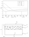
- Figure 1 shows the reference reflectance (RR) curves in a wavelength ( ⁇ ) range from 800 nm to 2500 nm for three different substrates (101, 102, 103) for transmitting IR light according to certain embodiments of the present invention, compared to an non-treated substrate (100).
- Each of the three reference reflectance curves (101, 102, 103) shows a minimum reference reflectance at a certain wavelength ⁇ min (101), ⁇ min (102), and ⁇ min (103).
- the reference reflectance is reduced in the infrared wavelength range from 800 nm to 3 ⁇ m, with a minimum at the wavelength ⁇ min when the ions are implanted with an acceleration voltage AV such that ratio of the acceleration voltage AV to the average standard atomic weight Z avr of the implanted ions is comprised in the range from 0.0029 ⁇ ⁇ min ⁇ kV/nm - 1.25 kV to 0.0026 ⁇ ⁇ min ⁇ kV/nm + 0.68 kV, with ⁇ min being wavelength of the minimum of the reference reflectance in the infrared wavelength range from 800 nm to 3 ⁇ m.
- the present invention in certain embodiments, also concerns the use of a bi-layer within a substrate, to reduce the reference reflectance of the substrate in the wavelength range from 800 nm to 3 ⁇ m.
- the bi-layer comprises, starting from the substrate surface and going towards the core of the substrate, a first layer having almost the same refractive index as the bulk substrate, and a porous second layer, having a refractive index lower than the bulk substrate.
- the first layer has a refractive index n 1 where 0.95 ⁇ n b ⁇ n 1 ⁇ 1.05 ⁇ n b , n b being the refractive index of the bulk substrate, and the second layer has a refractive index n2, wherein n 2 ⁇ n b , the refractive index being the average refractive index in the wavelength range from 800 nm to 3 ⁇ m.
- the solid phase of first and second layers that is the part of the first and second layers that is not a pore, consists essentially of the same material as the bulk material of the substrate.
- the same material in the present case means that the material is the same except for components, such as alkali-ions, that may be present in the substrate and that are susceptible to migrate towards the core of the substrate upon ion implantation.
- Figure 2 shows an exemplary embodiment (not to scale) of a substrate for transmitting infrared light (200), having, starting from the substrate surface (204) and going towards the core of the substrate (205), a first layer (201) having the same refractive index as the bulk substrate, and a porous second layer (202), having a refractive index lower than the bulk substrate.
- the first layer has a thickness t 1 and the porous second layer has a thickness t 2 .
- the first layer has no detectable porosity.
- the lower size limit of detectability of pores is about 3 nm in diameter.
- the pores of the porous second layer are filled with the gas formed by recombination of the implanted ions. Implanted ions formed from the same gas are to be found throughout the solid material of the first layer at a concentration of less than 10 atom %.
- the refractive index is the average refractive index in the wavelength range from 800 nm to 3 ⁇ m.
- the first layer may have a thickness t 1 in the range from 10 nm to 120 nm, the porous second layer having a thickness t 2 in the range from 110 nm to 400 nm and the ratio t 2 /t 1 being in the range from 3 to 11. All thicknesses herein are geometrical, or physical thicknesses unless otherwise noted.
- the porous second layer may have a pore density in the range from 15 to 80%, advantageously in the range from 25 to 70 %, more preferably in the range from 25 to 65%.
- the pore density is determined on a TEM image of a cross section of the porous layer as explained below. Higher pore density is beneficial for low reference reflectance, but tends to reduce the mechanical durability of the treated substrate. A good compromise between reference reflectance reduction and mechanical durability is obtained with the pore density in the range from 30 to 60%, in particular when combined with the layer thicknesses hereinabove.
- the reference reflectance is reduced in the infrared wavelength range from 800 nm to 3 ⁇ m, with a minimum at the wavelength ⁇ min when the first layer has a thickness in the range from 0.04 ⁇ ⁇ min - 21 nm to 0.04 ⁇ ⁇ min - 15 and the porous second layer has a thickness in the range from 0.11 ⁇ ⁇ min + 24 nm to 0.11 ⁇ ⁇ min + 88 nm, with ⁇ min being wavelength of the minimum of the reference reflectance in the infrared wavelength range from 800 nm to 3000 nm.
- the average reference reflectance in the wavelength range from 800 nm and 1600 nm is reduced by 1%, in particular by 2%, and even by 3% of the total incoming light.
- ⁇ min is in the wavelength range from 800 nm to 1200 nm, in particular from 900 to 1100 nm. It was found that the treated substrate of the present invention then has a neutral or green-blue color in reflection.
- the CIELAB color coordinates of the reflected light on the ion implanted side of the substrate is neutral or blue-green, that is -10 ⁇ a* Rc ⁇ 1 and -20 ⁇ b* Rc ⁇ 1, or is closer to neutral or has a less intense blue-green tint, that is -5 ⁇ a* Rc ⁇ 0.5 and -15 ⁇ b* Rc ⁇ 0.5, or even is very neutral or has a slight blue-green tint, that is -4 ⁇ a* Rc ⁇ 0 and -10 ⁇ b* Rc ⁇ 0.
- the substrate is chosen among soda-lime-silica glass, alumino-silicate glass and boro-silicate glass.
- the substrate may be a plano-optic substrate, for example a window, mirror, polarizer, beamsplitter, or prism, a spherical lens, for example a plano-concave/convex, doubleconcave/convex, or meniscus lens, an aspheric lens, for example a parabolic, hyperbolic, or hybrid lens, or an achromatic lens.
- the substrate may be part of an optical assembly, for example an imaging lens, a beam expander, an eyepiece, an objectives, or glasses.
- the substrate of the present invention may in particular be a window or a lens for transmitting infrared light from an infrared lamp or an infrared laser, for example a laser emitting infrared light in the wavelength range from 800 nm to 1.6 ⁇ m.
- the substrate may be a substrate to transmit of an infrared laser of a wavelength ⁇ L , preferably the substrate has a minimum of reflectance at a wavelength ⁇ min , where 0.95 ⁇ L ⁇ ⁇ min ⁇ 1.05 ⁇ L .
- the temperature of the substrate is kept during implantation below the glass-transition temperature of the substrate.
- the temperature is kept below 600° C, more preferably below 500° C, most preferably below 400° C.
- the glass composition of the substrate of the present invention comprises, expressed on oxide basis as percentages by weight total glass: SiO 2 55-85%, Al 2 O 3 0-30%, B 2 O 3 0-20%, Na 2 O 0-25%, CaO 0-20%, MgO 0-15%, K 2 O 0-20%, BaO 0-20%.
- the glass composition of the optical element of the present invention comprises, expressed on oxide basis as percentages by weight total glass: SiO 2 55-78%, Al 2 O 3 0-18%, B 2 O 3 0-18%, Na 2 O 0-20%, CaO 0-15%, MgO 0 - 10%, K 2 O 0 - 10%, BaO 0-5%.
- the borosilicate glass composition of the optical element of the present invention comprises, expressed on oxide basis as percentages by weight total glass: SiO 2 60-70 %, B 2 O 3 10-20 %, K 2 O 5-15 %, Na 2 O 1-15 %, BaO 1-10 %, Sb 2 O 3 ⁇ 1 %, CaO ⁇ 1 %, TiO 2 ⁇ 1 %, ZnO ⁇ 1 %.
- this borosilicate glass composition further comprises 1 to 5% by weight of CeO 2 , for increased resistance to radiation, in particular ionizing radiation.
- the glass of the optical element of the present invention comprises, for reasons of lower production costs, is soda-lime glass.
- the glass composition of the optical element of the present invention comprises, expressed on oxide basis as percentages by weight total glass: SiO 2 60-75%, Al 2 O 3 0-6%, B 2 O 3 0-4%, Na 2 O 5-20%, CaO 0-15%, MgO 0-10%, K 2 O 0-10%, BaO 0-5%.
- the glass may comprise other components, nature and amount of which may vary depending on the desired effect.
- the glass composition of the optical element of the present invention further comprises chromium, in a range of specific contents.
- the glass composition of the optical element of the present invention further comprises, expressed on oxide basis as percentages by weight total glass: Total iron (expressed as Fe 2 O 3 ) 0.002 to 0.06%, Cr 2 O 3 0.0001 to 0.06%.
- Such glass compositions combining low levels of iron and chromium show particularly good performance in terms of infrared transmittance as well as transmittance in the visible range and neutral colors in transmittance.
- Exemplary glass compositions thereof are described in international applications: WO2014128016A1 , WO2014180679A1 , WO2015011040A1 , WO2015011041A1 , WO2015011042A1 , WO2015011043A1 , and WO2015011044A1 .
- these glass compositions advantageously comprise chromium (expressed as Cr 2 O 3 ) ranging from 0.002 to 0.06% by weight relative to the total weight of the glass. Such chromium contents can further improve the infrared transmittance.
- the glass composition of the optical element of the present invention further comprises, expressed on oxide basis as percentages by weight total glass: Total iron (expressed as Fe 2 O 3 ) 0.002 to 0.06%, Cr 2 O 3 0.0015 to 1%, Co 0.0001 to 1%.
- Such chromium and cobalt-based glass compositions show particularly good performance in terms of infrared transmittance, while offering interesting possibilities in terms of aesthetics or color (from blue to neutral intense staining or until 'opacity).
- Exemplary compositions hereof are disclosed in Patent Application WO2015091106 A1 .
- the glass composition of the optical element of the present invention further comprises, expressed on oxide basis as percentages by weight total glass: Total iron (expressed as Fe 2 O 3 ) 0.002 to 1%, Cr 2 O 3 0.002 to 0.5%, Co 0.0001 to 0.5%
- the composition comprises: 0.06% ⁇ Total iron ⁇ 1%.
- compositions based on chromium and cobalt may be used to obtain colored glass sheets in the blue-green range, comparable in terms of color and light transmission with traditional soda-lime based blue and green glasses, but with particularly high infrared transmittance.
- the glass composition of the optical element of the present invention further comprises, expressed on oxide basis as percentages by weight total glass: Total iron (expressed as Fe 2 O 3 ) 0.002 to 1%, Cr 2 O 3 0.002 to 0.5%, Co 0.0001 to 0.5%, Se 0.0003 to 0.5%.
- Such glass compositions based on chromium, cobalt and selenium have shown particularly good performance in terms of infrared transmittance, while offering interesting possibilities in terms of aesthetics / color (gray neutral to slight staining intense in the graybronze range).
- Such compositions are disclosed in Patent Application WO2016202689 A1 .
- the glass composition of the optical element of the present invention further comprises other components in specific concentrations to further increase transmittance of IR light.
- the glass composition of the optical element of the present invention further comprises, expressed on oxide basis as percentages by weight total glass: Total iron (expressed as Fe 2 O 3 ) 0.002 to 0.6%, CeO 2 0.001 to 1%.
- compositions are disclosed in Patent Application WO2015071456 A1 .
- the glass composition of the optical element of the present invention further comprises, expressed on oxide basis as percentages by weight total glass: Total iron (expressed as Fe 2 O 3 ) 0.002 to 0.06%, and one of the following components:
- compositions are disclosed in Patent Application WO2015172983 A1 .
- the glass composition of the optical element of the present invention further comprises, expressed on oxide basis as percentages by weight total glass: Total iron (expressed as Fe 2 O 3 ) 0.002 to 0.04%, and one of the and at least two components among chromium, selenium, copper, cerium, manganese and antimony; with chromium (expressed as Cr 2 O 3 ) being a maximum content of 0.02% by weight; selenium (expressed as Se) being a maximum content of 0.08% by weight; copper (expressed as CuO) being a maximum content of 0.04% by weight; cerium (calculated as CeO 2 ) being a maximum content of 0.8% by weight; manganese (calculated as MnO) being a maximum content of 1.6% by weight; antimony (expressed as Sb 2 O 3 ) being a maximum content of 0.8% by weight; said composition having the formula: A ⁇ [10.02 * (Cr 2 O 3 / Fe 2 O 3 ) + 4
- compositions are disclosed in European Patent Application No. WO2016008906 A1 .
- the composition of the glass sheet has a redox of less than 15%.
- the redox is lower than 10%, or less than 5% or even less than 3%.
- the degree of oxidation of a glass is given by the redox, defined as the ratio of atom weight of Fe 2+ based on the total weight of iron atoms Fe tot present in the glass, Fe 2+ / Fe tot .
- the ion implantation of the present invention may lead to a less steep increase of reference reflectance towards wavelengths ⁇ ⁇ min , in particular when compared to the ion implantation of single charge ions only.
- the ion implantation of the present invention may lead to a less high increase of reference reflectance towards wavelengths ⁇ ⁇ min , in particular when compared to the ion implantation of single charge ions only.
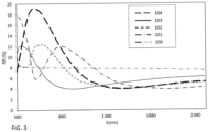
- Figure 3 shows the reference reflectance (RR) curves in a wavelength ( ⁇ ) range from 380 nm to 2500 nm for three different substrates (101, 102, 103) for transmitting IR light according to certain embodiments of the present invention, of a non-treated substrate (100) and of a treated substrate (104), not according to the present invention, implanted with Kr + single charge ions at an energy of 200keV and a dosage of 2.5 x 10 16 ions/cm 2 .
- the reference reflectance curves of substrates treated according to the present invention show, in particular in comparison with substrate (104), a flat reflectance curve, a limited increase of reflectance in the visible wavelength range, and a less steep increase of reflectance towards wavelengths that are smaller than the wavelength of minimum reference reflectance.
- the RR curve of substrate (104) is extrapolated from reflectance data reported in POLATO Pietro. et al., Characterization by Nuclear and Spectrophotometric Analysis of Near - Surface Modifications of Glass Implanted with Heavy Ions, Journal of the American Chemical Society, vol. 70, no.10, pages 775-779 .
- the ion implantation leads to a limited increase of reference reflectance in the visible light range.
- the reference reflectance of a treated substrate at a wavelength ⁇ -500 does not rise above 13%.
- the reference reflectance of a treated substrate does not rise above 13% in the visible light range of wavelengths between 380nm and 780nm.
- the ion implantation furthermore results in a reduction of the visible light reference reflectance, in particular for ⁇ min ⁇ 1100nm, more particularly for ⁇ min ⁇ 1000nm.
- the reference reflectance in the visible range of a treated substrate is at most 7%, in particular for ⁇ min ⁇ 1100nm, more particularly for ⁇ min ⁇ 1000nm..
- the bulk temperature of the area of the glass substrate being treated, situated under the area being treated is less than or equal to the glass transition temperature of the glass substrate.
- This temperature is for example influenced by the ion current of the beam, by the residence time of the treated area in the beam and by any cooling means of the substrate.
- the implantation of ions according to the present invention is preferably performed in a vacuum chamber at a pressure comprised between 10 -7 mbar and 10 -2 mbar, more preferably at a pressure comprised between 5 ⁇ 10 -5 mbar and 2 ⁇ 10 -6 mbar.
- pores of the porous second layer are filled with a gas. Ions formed of the same gas are to be found throughout the solid material both the first and the porous second layers.
- An example ion source for carrying out the method of the present invention is the Hardion+ ECR ion source from Ionics SA.
- the present invention also concerns the use of a mixture of single charge and multicharge ions of N, H, O, He, Ne, Ar, or Kr to decrease the reference reflectance of an etched glass substrate, the mixture of single charge and multicharge ions being implanted in the glass substrate with an ion dosage and acceleration voltage effective to reduce the reference reflectance of the glass substrate.
- the implantation depth of the ions may be comprised between 0.11 ⁇ m and 1 ⁇ m, preferably between 0.15 ⁇ m and 0.5 ⁇ m.
- the implanted ions are spread between the substrate surface and the implantation depth.
- the implantation depth may be adapted by the choice of implanted ion, by the acceleration energy and varies to a certain degree depending on the substrate.
- the mixture of single charge and multicharge ions of O or N preferably comprises, O + and O 2+ or N + , N 2+ and N 3+ respectively.
- mixture of single charge and multicharge ions of O comprises a lesser amount of O 2+ than of O + .
- the mixture of single charge and multicharge ions of O comprises 55-98% of O + and, 2-45% of O 2+ .
- mixture of single charge and multicharge ions of N comprises a lesser amount of N 3+ than of N + and of N 2+ each.
- the mixture of single charge and multicharge ions of N comprises 40-70% of N + , 20-40% of N 2+ , and 2-20% of N 3+ .
- the glass sheet of the invention is a glass sheet formed by a slot draw process or by a fusion process, in particular the overflow downdraw fusion process.
- a fusion process in particular the overflow downdraw fusion process.
- the substrate according to the invention may have a thickness of from 0.1 to 25 mm.
- the glass sheet according to the invention has preferably a thickness of from 0.1 to 6 mm. More preferably, in the case of display applications and for reasons of weight, the thickness of the glass sheet according to the invention is of from 0.1 to 2.2 mm.
- the substrate according to the invention may have a thickness of from 10 ⁇ m to 100 ⁇ m, advantageously from 50 ⁇ m to 100 ⁇ m.
- Another additional objective of the invention is to provide an optical assembly for emitting, detecting or measuring infrared light at a wavelength ⁇ L in the range between 800 nm and 3 ⁇ m comprising
- Infrared sensitive optical components may comprise an IR detector, such as a motion sensor or a pyrometer for example, an imaging sensor, such as a charge coupled device or a microbolometer array,
- Infrared light sources may be infrared lasers or lamps for example. It may also be a hot object, emitting thermal radiation in the infrared range.
- the optical assembly may comprise both an infrared light source and an infrared sensitive optical component, such as in a light detection and ranging (LIDAR) device.
- LIDAR light detection and ranging
- the optical assembly of the present invention may also comprise additional optical elements, such as for example lenses, prisms, or covers. These may be substrates according to the present invention or not.
- the microstructure of the treated substrates, the layer thicknesses and in particular pore density were investigated by Transmission Electron Microscope (TEM). Cross-sectional specimens were prepared using Focused In Beam (FIB) procedure. During the preparation process carbon and platinum protective layers were deposited on top of the film.
- TEM Transmission Electron Microscope
- FIB Focused In Beam
- the pore densities as determined by the present method on a two-dimensional image are considered to be representative of the three-dimensional size and densities of the pores.
- the images from the TEM were processed with image analysis software ImageJ (developed by the National Institutes of Health, USA) to identify the pores as well-defined bright areas.
- ImageJ developed by the National Institutes of Health, USA
- the cross-sectional equivalent circular diameter of a pore is the diameter of a two-dimensional disk having an equivalent area to the cross-section of the pore as determined by this image analysis method.
- the pore density was evaluated as the percentage of the cross-section area of the porous second layer occupied by pores.
- the layer thicknesses were also evaluated on the TEM micrographs.
- the ion implantation examples were prepared according to the various parameters detailed in the tables below using an ECR ion source for generating a beam of a mixture of single charge and multicharge ions.
- the ion source used was a Hardion+ ECR ion source from Ionics S.A.
- All samples had a size of about 100 cm 2 and were treated on the entire surface by displacing the substrate through the ion beam at a speed selected between 10 and 100 mm/s.
- the temperature of the area of the substrate being treated was kept at a temperature less than or equal to the melting temperature of the substrate.
- the implantation was performed in a vacuum chamber at a pressure of 10 -6 mbar.
- ions of N were implanted in 1.6 mm thick substrates of normal clear soda lime glass.
- the average reference reflectance (avg RR) of the glass substrates in the wavelength range from 800 nm to 2.5 ⁇ m was 7.7%.
- the key implantation parameters can be found in table 1 below. Table 1 also shows for each sample the average reference reflectance (avg RR), the wavelength of minimum reference reflectance ⁇ min , and the reference reflectance (RR) at ⁇ min .
- Table 2 shows acceleration voltages leading each to comparable results for implanted ions N, He, or Kr.
- Table 2 Source gas Acceleration voltage ⁇ min RR at ⁇ min t1 t2 Pore density [kV] [nm] [%] [nm] [nm] [%] N 2 35 1000 3.9 25 145 60 He 10 Kr 170 N 2 55 1500 3.9 40 210 60 He 14 Kr 250 N 2 70 2000 3.9 52.5 287.5 60 He 20 Kr 350 N 2 90 2500 3.8 87.5 387.5 60 He 25 Kr 400
- Table 3 sample numbe r RR at ⁇ -500 ⁇ -500 Max. RR from 380nm to 780nm [%] [nm] [%] E1 7.1 370 6.7 E2 8.1 305 7.6 E3 9.9 360 8.8 E4 10.7 360 9.6 E5 9.5 380 9.5 E6 13.0 380 13.0 E7 11.7 380 11.7
Landscapes
- Physics & Mathematics (AREA)
- Chemical & Material Sciences (AREA)
- Engineering & Computer Science (AREA)
- General Physics & Mathematics (AREA)
- Geochemistry & Mineralogy (AREA)
- Life Sciences & Earth Sciences (AREA)
- Chemical Kinetics & Catalysis (AREA)
- General Chemical & Material Sciences (AREA)
- Materials Engineering (AREA)
- Organic Chemistry (AREA)
- Spectroscopy & Molecular Physics (AREA)
- Toxicology (AREA)
- Plasma & Fusion (AREA)
- Health & Medical Sciences (AREA)
- Optics & Photonics (AREA)
- Glass Compositions (AREA)
- Analytical Chemistry (AREA)
- Surface Treatment Of Optical Elements (AREA)
- Surface Treatment Of Glass (AREA)
Description
- The present invention relates to substrates that can act as optical elements for transmitting infrared light and that have low reflectance for infrared light. The substrates of the present invention are suitable for cover glasses and optical elements, such as lenses, prisms, or mirrors to be used with infrared light. In particular the invention relates to the Use of implanted ions implanted into a substrate in order to reduce its reflectance of infrared light and also relates to an assembly of such a substrate with a source of infrared light and/or with an infrared-sensitive optical component.
- A variety of applications, ranging from the detection of infrared (IR) signals, for instance in thermal imaging, to element identification in IR spectroscopy, make use of infrared light. A certain range of substrates is being used to manufacture optical elements that transmit, reflect and/or generally control the trajectory of IR light, such as plano-optics (i.e. windows, mirrors, polarizers, beamsplitters, prisms), spherical lenses (i.e. plano-concave/convex, double-concave/convex, meniscus), aspheric lenses (parabolic, hyperbolic, hybrid), achromatic lenses, and lens assemblies (i.e. imaging lenses, beam expanders, eyepieces, objectives). The bulk materials of these substrates for infrared applications vary in their physical, in particular optical, characteristics. As a result, knowing the benefits of each characteristic allows one to select the correct material for any IR application. Since infrared light is comprised of longer wavelengths than visible light, the two wavelength regions, visible and infrared, behave differently when propagating through the same optical medium. In general, certain materials can be used for both IR and visible applications, most notably fused silica, borosilicate glass, sapphire, alumina-silicate glass and certain soda-lime glasses, while others are used only for one or the other application. The foremost attribute defining any bulk material for infrared light is transmittance of infrared light. Transmittance is a measure of throughput and is given as a percentage of the incident light.
- Optical elements for infrared light comprise a substrate and may further comprise coatings. Anti-reflection (AR) coatings are frequently used to improve the efficiency of optical elements by increasing transmission of infrared light, enhancing contrast, and eliminating ghost images. These AR coatings generally need to be durable, with resistance to both physical and environmental damage and they range from single layer coatings, of intermediate index between that of air and the substrate, to complex multi-layer stacks of alternating high refractive index and low refractive index layers. The multi-layer stacks, although effective to reduce IR reflectance, they require expensive equipment, generally have lower durability than the substrate itself.
- For certain applications, a compromise must be made regarding the wavelength range in which the reflectance can be lowered by common AR coatings. In particular, it is difficult to obtain anti-reflective coatings for infrared radiation, in particular near-infrared light in the range between 800 nm and 3 µm, while maintaining low visible light reflectance and/or reflected light colors that are close to neutral or have a blue-green tint.
-
EP0318440 discloses a process for the manufacture of glass capable of transmitting and reflecting radiant energy in an amount different from that transmitted and reflected by the original glass.US2017/114442 discloses a treatment method for modifying the reflected colour of a sapphire material surface. - The objective of the invention in particular is to remedy one or more of the cited disadvantages, i.e. to provide a substrate, in particular an ion implanted substrate, with lower reflectance in the infrared light range, in particular in the wavelength range between 800 nm and 3 µm, in particular between 800 nm and 2.5 µm and at the same time limit or even avoid increasing the reflectance of light in the visible light wavelength range. The substrate according to the present invention is a substrate for transmitting infrared light.
- An additional objective of the present invention, in certain of its embodiments, is to provide an ion implanted substrate for transmitting infrared light with lower reflectance in the infrared light range between 800 nm and 3 µm and with a neutral or blue-green color in reflection.
- Another additional objective of the present invention, in certain of its embodiments, is the use of implanted ions implanted into a substrate at certain acceleration voltages and dosages, to reduce the reference reflectance of an a substrate for an optical element in the infrared light range between 800 nm and 3 µm glass sheet. The resulting substrate or optical element has a lower reflectance in the infrared wavelength range from 800 nm to 3 µm, meaning that its reference reflectance in this infrared wavelength range is lower than the reference reflectance of the untreated substrate.
- Another additional objective of the invention is to provide an optical assembly for controlling infrared light in the range between 800 nm and 3 µm comprising an ion implanted optical element for transmitting the infrared light having low reflectance in the infrared light range between 800 nm and 3 µm and an infrared sensitive optical component and/or an infrared light source.
- According to the present invention one or more of these objectives are obtained by ion implantation, with a mixture of single charge and multicharge ions, of at least part of the surface of the substrate forming the optical element.
- The inventors have surprisingly found that implanting substrates with ions of certain atoms at certain acceleration voltages and certain dosages lowers the reflectance of the substrates in the infrared wavelength range from 800 nm to 3µm.
- The inventors have also found that implanting substrates with ions of certain atoms at certain acceleration voltages and certain dosages leads to the formation of a bi-layer structure within the substrate, at the substrate surface. The bi-layer comprises, starting from the substrate surface and going towards the core of the substrate, a first layer having the same refractive index as the bulk substrate, and a porous second layer, having a refractive index lower than the bulk substrate. The solid material forming the 1st layer and porous second layer consists essentially of the same material as the substrate bulk.
- The present invention also concerns the use of implanted ions implanted into a substrate for reducing the substrate's reflectance of infrared light in the wavelength range from 800nm to 3µm, in particular from 800 nm to 2.5 µm.
- It is noted that the invention relates to all possible combinations of features recited in the claims.
-
-
FIG. 1 shows reference reflectance curves in the infrared light range of three exemplary substrates for transmitting infrared light according to the present invention and one non-treated substrate. -
FIG. 2 shows a schematic cross-section of a substrate according to the present invention. -
FIG. 3 shows reference reflectance curves in the visible and infrared light ranges of three exemplary substrates for transmitting infrared light according to the present invention and for one non-treated substrate and for one ion implanted substrate not according to the present invention. - The invention relates to the use of implanted ions to decrease the infrared reflectance of a substrate for transmitting infrared light, in particular in the wavelength range from 800 nm to 3 µm, where ions are implanted in the substrate.
- According to the present invention, the ion implantation comprises the implantation of positively charged ions of N, H, O, He, Ne, Ar or Kr. According the present invention the positively charged implanted ions comprise a mixture of single and multiple charged ions. Advantageously the ion implantation comprises the implantation of positively charged ions of N, H, O, or He as they require lesser acceleration voltages.
- Preferred statements (features) and embodiments of uses of this invention and articles comprising this invention are set herein below. Each statement and embodiment of the invention so defined may be combined with any other statement and/or embodiment, unless clearly indicated to the contrary. In particular, any feature indicated as being preferred or advantageous may be combined with any other features or statements indicated as being preferred or advantageous.
- According to an embodiment of the present invention the implanted substrate of the present invention comprises no other layers than the bi-layer structure at the implanted surface of the substrate.
- It was found that the degree of infrared light reflectance can be varied by varying the amount of ions implanted and their implantation depth.
- According to an embodiment of the present invention, the ion dosage is comprised between 1016 ions/cm2 and 2 × 10¹⁷ ions/cm2, advantageously between 1016 ions/cm2 and 1.5 × 10¹⁷ ions/cm2, more advantageously between 1016 ions/cm2 and 9.5 × 10¹⁶ ions/cm2. Within these ranges, the dosage may be at least 2 × 10¹⁶ ions/cm2, at least 4 × 10¹⁶ ions/cm2 or even at least 6 × 10¹⁶ ions/cm2. The ion dosage may for example be controlled by the duration of exposure to the ion beam and also depends on the fluence of the beam.
- Implanted ions may be present in the substrate beyond the porous second layer. According to an embodiment of the present invention, no additional porous layer, other than the porous second layer, is present in the substrates of embodiments of the present invention. According to another embodiment of the present invention, one additional porous third layer, is present in a substrate, having a pore density different from the pore density of the porous second layer.
- The implantation depth may be controlled by the acceleration voltage of the ion source for a given ion or ion mixture.
- Electron Cyclotron Resonance (ECR) ion sources providing an ion beam comprising a mixture of single charged ions and multi charged ions are particularly useful as for a certain acceleration voltage, a double charged ion of a certain species, for example N2+, will have double the implantation energy of the corresponding single charge ion, N+. Thereby greater implantation depths can be reached without having to increase the acceleration voltage. The inventors have found that ion sources providing an ion beam comprising a mixture of single charge and multicharge ions, accelerated with the same acceleration voltage are particularly useful as they may provide higher fluences than single charge ion beams. They are therefore able to reach a certain dosage in a shorter amount of time. According to the present invention the ECR ion source may provide an ion current of at least 0.5 mA, advantageously at least 0.8 mA, more advantageously at least 1.0 mA and not more than 50mA.
- In an embodiment of the present invention the ion beam at least 90% of the ions in the ion beam comprise single charge and double charge ions of a species selected from N, O, He, Ne, Ar, and Kr and the ratio of single charge species and double charge species is at least 55/25. The respective single charge and double charge species are N+ and N2+, O+ and O2+, He+ and He2+, Ne+ and Ne2+, Ar+ and Ar2+, Kr+ and Kr2+. Hydrogen is only available as single charge ion H+.
- In certain embodiments the substrate being implanted is moved relative to the ion beam in order to treat its entire surface.
- According to the present invention the substrate may comprise a flat, sheet-like, substrate or a non-flat substrate, such as a prism or a lens. The substrate may be obtained by casting, cutting, bending, grinding or pressing to obtain the desired shape, before undergoing ion implantation.
- Measuring the reflection and comparing reflectance values on optical elements that are not flat is very complicated. Therefore and for the purpose of the present text, the term of 'reference reflectance' is defined and used for all substrates when appropriate. The reference reflectance of a substrate is the reflectance of a 1.6 mm thick flat sheet of the substrate's material, treated by the same ion implantation when appropriate, or comprising the same bi-layer when appropriate. The reference reflection is measured on the surface that has been ion implanted as the percentage of incoming light that is reflected from the surface at an 8° angle. The average reference reflectance is calculated by averaging of the measurement values over the selected wavelength range.
- The reference color in reflection is calculated from this measurement and is expressed using CIELAB color coordinates a* and b* under illuminant D65 using 10° observer angle. CIE L*a*b* or CIELAB is a color space specified by the International Commission on Illumination and is routinely used in glass industry among others. Unless specified otherwise, the visible light reference reflectance Rc, and the reference colors in reflection a*Rc, b*Rc are measured at an angle of 8° , close to perpendicular to the substrate surface.
- Reflectance is routinely measured using spectrophotometers operating in the appropriate wavelength range. In the examples below measurements were made up to a wavelength of 2.5 µm. Optical simulations show that reflectance values at least up to 3µm wavelength can be extrapolated from these measurements.
- Throughout the present text, when a numerical range is indicated, the limits of the range are considered to be included in the range. In addition, all the integral and subdomain values in the numerical range are expressly included as if explicitly written.
- Depending on the application it may be relevant to obtain a low infrared (IR) reference reflectance over as much as possible of the IR wavelength range from 800 nm to 3 µm, or it may be relevant to reduce the reference reflectance as much as possible at a certain wavelength λ min, where λ min is in the range from 800 nm to 3 µm.
- According to an embodiment of the present invention, the reference reflectance of a substrate in the infrared wavelength range, in particular in the wavelength range from 800 nm to 3 µm, is reduced by using an ion implantation process comprising the following operations:
- a. providing a source gas selected among N2, H2, O2, He, Ne, Ar, and Kr,
- b. ionizing the source gas so as to form ions of N, O, He, Ne, Ar, or Kr, wherein the ions comprise a mixture of single charge and multicharge ions of N, O, He, Ne, Ar, or Kr.
- c. accelerating the ions with an acceleration voltage so as to form a beam, wherein the first acceleration voltage is comprised between 5.5 and 450 kV, and
- d. positioning a surface of the substrate in the trajectory of the beam so as to obtain an ion dosage comprised between 1016 ions/cm2 and 2 × 10¹⁷ ions/cm2.
- The inventors have found that the reference reflectance in the infrared wavelength range, in particular between 800nm and 3 µm, may be reduced. In particular the average reference reflectance between 800nm and 3 µm.
- The implantation of ions according to the present invention may reduce the average reference reflectance of a substrate, in the wavelength range from 800 nm to 3 µm, by at least 1%, advantageously by at least 2%, more advantageously by at least 3%.
- The inventors have found that the reference reflectance in the infrared wavelength range, in particular between 800nm and 3 µm, may be reduced to a minimum at a certain wavelength λ min, by using ions implanted with an acceleration voltage that depends on the standard atomic weight of the implanted ions. The standard atomic weight is the relative atomic mass as defined by the international union of pure and applied chemistry IUPAC. When a mixture of ions is implanted, be it a mixture of different isotopes or a mixture of ions from different chemical elements, the average standard atomic weight Zavr is the average of the relative atomic masses of the ions used.
-
Figure 1 shows the reference reflectance (RR) curves in a wavelength ( λ ) range from 800 nm to 2500 nm for three different substrates (101, 102, 103) for transmitting IR light according to certain embodiments of the present invention, compared to an non-treated substrate (100). Each of the three reference reflectance curves (101, 102, 103) shows a minimum reference reflectance at a certain wavelength λ min (101), λ min (102), and λ min (103). - According to an embodiment of the present invention, the reference reflectance is reduced in the infrared wavelength range from 800 nm to 3 µm, with a minimum at the wavelength λ min when the ions are implanted with an acceleration voltage AV such that ratio of the acceleration voltage AV to the average standard atomic weight Zavr of the implanted ions is comprised in the range from 0.0029 × λ min × kV/nm - 1.25 kV to 0.0026 × λ min × kV/nm + 0.68 kV, with λ min being wavelength of the minimum of the reference reflectance in the infrared wavelength range from 800 nm to 3 µm.
- The present invention, in certain embodiments, also concerns the use of a bi-layer within a substrate, to reduce the reference reflectance of the substrate in the wavelength range from 800 nm to 3 µm.
- The bi-layer comprises, starting from the substrate surface and going towards the core of the substrate, a first layer having almost the same refractive index as the bulk substrate, and a porous second layer, having a refractive index lower than the bulk substrate. The first layer has a refractive index n1 where 0.95 × nb ≤ n1 ≤ 1.05 × nb, nb being the refractive index of the bulk substrate, and the second layer has a refractive index n2, wherein n2 < nb, the refractive index being the average refractive index in the wavelength range from 800 nm to 3 µm. Preferably the solid phase of first and second layers, that is the part of the first and second layers that is not a pore, consists essentially of the same material as the bulk material of the substrate. Essentially the same material in the present case means that the material is the same except for components, such as alkali-ions, that may be present in the substrate and that are susceptible to migrate towards the core of the substrate upon ion implantation.
-
Figure 2 shows an exemplary embodiment (not to scale) of a substrate for transmitting infrared light (200), having, starting from the substrate surface (204) and going towards the core of the substrate (205), a first layer (201) having the same refractive index as the bulk substrate, and a porous second layer (202), having a refractive index lower than the bulk substrate. The first layer has a thickness t1 and the porous second layer has a thickness t2. - The first layer has no detectable porosity. The lower size limit of detectability of pores is about 3 nm in diameter. The pores of the porous second layer are filled with the gas formed by recombination of the implanted ions. Implanted ions formed from the same gas are to be found throughout the solid material of the first layer at a concentration of less than 10 atom %.
- For the purpose of the present invention the refractive index is the average refractive index in the wavelength range from 800 nm to 3 µm.
- In an embodiment of the present invention, the first layer may have a thickness t1 in the range from 10 nm to 120 nm, the porous second layer having a thickness t2 in the range from 110 nm to 400 nm and the ratio t2/t1 being in the range from 3 to 11. All thicknesses herein are geometrical, or physical thicknesses unless otherwise noted.
- In particular the porous second layer may have a pore density in the range from 15 to 80%, advantageously in the range from 25 to 70 %, more preferably in the range from 25 to 65%. The pore density is determined on a TEM image of a cross section of the porous layer as explained below. Higher pore density is beneficial for low reference reflectance, but tends to reduce the mechanical durability of the treated substrate. A good compromise between reference reflectance reduction and mechanical durability is obtained with the pore density in the range from 30 to 60%, in particular when combined with the layer thicknesses hereinabove.
- According to another embodiment of the present invention, the reference reflectance is reduced in the infrared wavelength range from 800 nm to 3 µm, with a minimum at the wavelength λ min when the first layer has a thickness in the range from 0.04 × λ min - 21 nm to 0.04 × λ min - 15 and the porous second layer has a thickness in the range from 0.11 × λ min + 24 nm to 0.11 × λ min + 88 nm, with λ min being wavelength of the minimum of the reference reflectance in the infrared wavelength range from 800 nm to 3000 nm.
- According to certain embodiments of the invention hereinabove the average reference reflectance of the substrate in the IR wavelength range from 800 nm to 3 µm, in particular from 800 nm to 2.5 µm, is reduced by 1%, in particular by 2%, and even by 3% of the total incoming light.
- According to an embodiment of the present invention the reference reflectance of the substrate at a selected wavelength λ min in the IR wavelength range from 800 m to 3 µm, in particular from 800 nm to 2.5 µm, is reduced by 1.5%, in particular by 2.5%, and even by 3.5% of the total incoming light.
- According to an embodiment of the present invention the average reference reflectance in the wavelength range from 800 nm and 1600 nm is reduced by 1%, in particular by 2%, and even by 3% of the total incoming light.
- According to certain embodiments of the invention λ min is in the wavelength range from 800 nm to 1200 nm, in particular from 900 to 1100 nm. It was found that the treated substrate of the present invention then has a neutral or green-blue color in reflection. In particular the CIELAB color coordinates of the reflected light on the ion implanted side of the substrate, expressed by the color coordinates of a*Rc and b* Rc in reflection, is neutral or blue-green, that is -10 ≤ a* Rc ≤ 1 and -20 ≤ b* Rc ≤ 1, or is closer to neutral or has a less intense blue-green tint, that is -5 ≤ a* Rc ≤ 0.5 and -15 ≤ b* Rc ≤ 0.5, or even is very neutral or has a slight blue-green tint, that is -4 ≤ a* Rc ≤ 0 and -10 ≤ b* Rc ≤ 0.
- According to the present invention the substrate is chosen among soda-lime-silica glass, alumino-silicate glass and boro-silicate glass.
- According to the present invention the substrate may be a plano-optic substrate, for example a window, mirror, polarizer, beamsplitter, or prism, a spherical lens, for example a plano-concave/convex, doubleconcave/convex, or meniscus lens, an aspheric lens, for example a parabolic, hyperbolic, or hybrid lens, or an achromatic lens. According to the present invention the substrate may be part of an optical assembly, for example an imaging lens, a beam expander, an eyepiece, an objectives, or glasses. The substrate of the present invention may in particular be a window or a lens for transmitting infrared light from an infrared lamp or an infrared laser, for example a laser emitting infrared light in the wavelength range from 800 nm to 1.6 µm. In particular the substrate may be a substrate to transmit of an infrared laser of a wavelength λ L , preferably the substrate has a minimum of reflectance at a wavelength λ min, where 0.95 λ L ≤ λ min ≤ 1.05 λ L.
- According to advantageous embodiments of the present invention the temperature of the substrate is kept during implantation below the glass-transition temperature of the substrate. Preferably the temperature is kept below 600° C, more preferably below 500° C, most preferably below 400° C.
- In particular, the glass composition of the substrate of the present invention comprises, expressed on oxide basis as percentages by weight total glass:
SiO2 55-85%, Al2O3 0-30%, B2O3 0-20%, Na2O 0-25%, CaO 0-20%, MgO 0-15%, K2O 0-20%, BaO 0-20%. - In another particular embodiment, the glass composition of the optical element of the present invention comprises, expressed on oxide basis as percentages by weight total glass:
SiO2 55-78%, Al2O3 0-18%, B2O3 0-18%, Na2O 0-20%, CaO 0-15%, MgO 0 - 10%, K2O 0 - 10%, BaO 0-5%. - In particular, the borosilicate glass composition of the optical element of the present invention comprises, expressed on oxide basis as percentages by weight total glass:
SiO2 60-70 %, B2O3 10-20 %, K2O 5-15 %, Na2O 1-15 %, BaO 1-10 %, Sb2O3 <1 %, CaO <1 %, TiO2 <1 %, ZnO <1 %. - Optionally this borosilicate glass composition further comprises 1 to 5% by weight of CeO2, for increased resistance to radiation, in particular ionizing radiation.
- In an advantageous embodiment, the glass of the optical element of the present invention comprises, for reasons of lower production costs, is soda-lime glass. Advantageously, according to this embodiment, the glass composition of the optical element of the present invention comprises, expressed on oxide basis as percentages by weight total glass:
SiO2 60-75%, Al2O3 0-6%, B2O3 0-4%, Na2O 5-20%, CaO 0-15%, MgO 0-10%, K2O 0-10%, BaO 0-5%. - In addition to its any of its compositions hereinabove, the glass may comprise other components, nature and amount of which may vary depending on the desired effect.
- Optionally, to further increase transmittance of IR light, the glass composition of the optical element of the present invention further comprises chromium, in a range of specific contents.
- Thus, according to an optional embodiment of the present invention, the glass composition of the optical element of the present invention further comprises, expressed on oxide basis as percentages by weight total glass:
Total iron (expressed as Fe2O3) 0.002 to 0.06%, Cr2O3 0.0001 to 0.06%. - Such glass compositions combining low levels of iron and chromium show particularly good performance in terms of infrared transmittance as well as transmittance in the visible range and neutral colors in transmittance. Exemplary glass compositions thereof are described in international applications:
WO2014128016A1 ,WO2014180679A1 ,WO2015011040A1 ,WO2015011041A1 ,WO2015011042A1 ,WO2015011043A1 , andWO2015011044A1 . In particular these glass compositions advantageously comprise chromium (expressed as Cr2O3) ranging from 0.002 to 0.06% by weight relative to the total weight of the glass. Such chromium contents can further improve the infrared transmittance. - Thus, according to another optional embodiment of the present invention, the glass composition of the optical element of the present invention further comprises, expressed on oxide basis as percentages by weight total glass:
Total iron (expressed as Fe2O3) 0.002 to 0.06%, Cr2O3 0.0015 to 1%, Co 0.0001 to 1%. - Such chromium and cobalt-based glass compositions show particularly good performance in terms of infrared transmittance, while offering interesting possibilities in terms of aesthetics or color (from blue to neutral intense staining or until 'opacity). Exemplary compositions hereof are disclosed in Patent Application
WO2015091106 A1 . - According to another optional embodiment of the present invention, the glass composition of the optical element of the present invention further comprises, expressed on oxide basis as percentages by weight total glass:
Total iron (expressed as Fe2O3) 0.002 to 1%, Cr2O3 0.002 to 0.5%, Co 0.0001 to 0.5% - Advantageously, according to this embodiment, the composition comprises: 0.06% < Total iron ≤ 1%.
- Such compositions based on chromium and cobalt may be used to obtain colored glass sheets in the blue-green range, comparable in terms of color and light transmission with traditional soda-lime based blue and green glasses, but with particularly high infrared transmittance. Exemplary compositions hereof disclosed in Patent Application
WO2016202606 A1 . - According to another optional embodiment of the present invention, the glass composition of the optical element of the present invention further comprises, expressed on oxide basis as percentages by weight total glass:
Total iron (expressed as Fe2O3) 0.002 to 1%, Cr2O3 0.002 to 0.5%, Co 0.0001 to 0.5%, Se 0.0003 to 0.5%. - Such glass compositions based on chromium, cobalt and selenium have shown particularly good performance in terms of infrared transmittance, while offering interesting possibilities in terms of aesthetics / color (gray neutral to slight staining intense in the graybronze range). Such compositions are disclosed in Patent Application
WO2016202689 A1 . - Optionally, as an alternative to chromium, the glass composition of the optical element of the present invention further comprises other components in specific concentrations to further increase transmittance of IR light.
- According to an alternate optional embodiment of the present invention, the glass composition of the optical element of the present invention further comprises, expressed on oxide basis as percentages by weight total glass:
Total iron (expressed as Fe2O3) 0.002 to 0.6%, CeO2 0.001 to 1%. - Such compositions are disclosed in Patent Application
WO2015071456 A1 . - According to another alternate optional embodiment of the present invention, the glass composition of the optical element of the present invention further comprises, expressed on oxide basis as percentages by weight total glass:
Total iron (expressed as Fe2O3) 0.002 to 0.06%, - manganese (expressed as MnO) in an amount ranging from 0.01 to 1% by weight;
- antimony (expressed as Sb2O3), in an amount ranging from 0.01 to 1% by weight;
- arsenic (expressed as As2O3), in an amount ranging from 0.01 to 1% by weight, or
- copper (expressed as CuO), in an amount ranging from 0.0002 to 0.1% by weight.
- Such compositions are disclosed in Patent Application
WO2015172983 A1 . - According to another alternate optional embodiment of the present invention, the glass composition of the optical element of the present invention further comprises, expressed on oxide basis as percentages by weight total glass:
Total iron (expressed as Fe2O3) 0.002 to 0.04%,
A ≤ [10.02 * (Cr2O3 / Fe2O3) + 4 * (Se / Fe2O3) + 2.73 * (CuO / Fe2O3) + 0.7 * (CeO2 / Fe2O3) + 0.23 * (MnO / Fe2O3) + 0.11 * (Sb2O3 / Fe2O3)]; A being equal to 0.30. - Such compositions are disclosed in European Patent Application No.
WO2016008906 A1 . - According to an advantageous embodiment of the invention, the composition of the glass sheet has a redox of less than 15%. Preferably, the redox is lower than 10%, or less than 5% or even less than 3%. The degree of oxidation of a glass is given by the redox, defined as the ratio of atom weight of Fe2+ based on the total weight of iron atoms Fetot present in the glass, Fe2+ / Fetot.
- The inventors surprisingly found that the ion implantation of a mixture of single charge and multicharge ions led to a reflectance curve that was very flat around λ min. In particular the ion implantation of the present invention may lead to a less steep increase of reference reflectance towards wavelengths < λ min, in particular when compared to the ion implantation of single charge ions only. In particular the ion implantation of the present invention may lead to a less high increase of reference reflectance towards wavelengths < λ min, in particular when compared to the ion implantation of single charge ions only.
-
Figure 3 shows the reference reflectance (RR) curves in a wavelength (λ) range from 380 nm to 2500 nm for three different substrates (101, 102, 103) for transmitting IR light according to certain embodiments of the present invention, of a non-treated substrate (100) and of a treated substrate (104), not according to the present invention, implanted with Kr+ single charge ions at an energy of 200keV and a dosage of 2.5 x 10¹⁶ ions/cm2. The reference reflectance curves of substrates treated according to the present invention show, in particular in comparison with substrate (104), a flat reflectance curve, a limited increase of reflectance in the visible wavelength range, and a less steep increase of reflectance towards wavelengths that are smaller than the wavelength of minimum reference reflectance. The RR curve of substrate (104) is extrapolated from reflectance data reported in POLATO Pietro. et al., Characterization by Nuclear and Spectrophotometric Analysis of Near - Surface Modifications of Glass Implanted with Heavy Ions, Journal of the American Chemical Society, vol. 70, no.10, pages 775-779. - In certain embodiments of the present invention, the ion implantation leads to a limited increase of reference reflectance in the visible light range.
- In an embodiment of the present invention, the reference reflectance of a treated substrate at a wavelength λ -500, wherein λ -500= λ min- 500nm, does not rise above 13%.
- In an embodiment of the present invention, the reference reflectance of a treated substrate does not rise above 13% in the visible light range of wavelengths between 380nm and 780nm.
- In an embodiment of the invention the ion implantation furthermore results in a reduction of the visible light reference reflectance, in particular for λ min ≤1100nm, more particularly for λ min ≤1000nm.
- According to certain embodiments, the reference reflectance in the visible range of a treated substrate is at most 7%, in particular for λ min ≤1100nm, more particularly for λ min ≤1000nm..
- In a preferred embodiment of the present invention the bulk temperature of the area of the glass substrate being treated, situated under the area being treated is less than or equal to the glass transition temperature of the glass substrate. This temperature is for example influenced by the ion current of the beam, by the residence time of the treated area in the beam and by any cooling means of the substrate.
- The implantation of ions according to the present invention is preferably performed in a vacuum chamber at a pressure comprised between 10-7 mbar and 10-2 mbar, more preferably at a pressure comprised between 5 × 10⁻⁵ mbar and 2 × 10⁻⁶ mbar.
- The pores of the porous second layer are filled with a gas. Ions formed of the same gas are to be found throughout the solid material both the first and the porous second layers.
- An example ion source for carrying out the method of the present invention is the Hardion+ ECR ion source from Ionics SA.
- The present invention also concerns the use of a mixture of single charge and multicharge ions of N, H, O, He, Ne, Ar, or Kr to decrease the reference reflectance of an etched glass substrate, the mixture of single charge and multicharge ions being implanted in the glass substrate with an ion dosage and acceleration voltage effective to reduce the reference reflectance of the glass substrate.
- Advantageously the implantation depth of the ions may be comprised between 0.11 µm and 1 µm, preferably between 0.15 µm and 0.5 µm. The implanted ions are spread between the substrate surface and the implantation depth. The implantation depth may be adapted by the choice of implanted ion, by the acceleration energy and varies to a certain degree depending on the substrate.
- According to the present invention, the mixture of single charge and multicharge ions of O or N preferably comprises, O+ and O2+ or N+, N2+ and N3+ respectively.
- According to a preferred embodiment of the present invention, mixture of single charge and multicharge ions of O comprises a lesser amount of O2+ than of O+. In a more preferred embodiment of the present invention the mixture of single charge and multicharge ions of O comprises 55-98% of O+ and, 2-45% of O2+.
- According to another preferred embodiment of the present invention, mixture of single charge and multicharge ions of N comprises a lesser amount of N3+ than of N+ and of N2+each. In a more preferred embodiment of the present invention the mixture of single charge and multicharge ions of N comprises 40-70% of N+, 20-40% of N2+, and 2-20% of N3+.
- According to another preferred embodiment, the glass sheet of the invention is a glass sheet formed by a slot draw process or by a fusion process, in particular the overflow downdraw fusion process. These processes, in particular the fusion process produces glass sheets whose surfaces may reach superior flatness and smoothness necessary in some applications, but they are also more expensive than the float process for large scale glass production.
- The substrate according to the invention may have a thickness of from 0.1 to 25 mm. Advantageously, in the case of display applications, the glass sheet according to the invention has preferably a thickness of from 0.1 to 6 mm. More preferably, in the case of display applications and for reasons of weight, the thickness of the glass sheet according to the invention is of from 0.1 to 2.2 mm.
- In certain applications the substrate according to the invention may have a thickness of from 10µm to 100 µm, advantageously from 50 µm to 100 µm.
- Another additional objective of the invention is to provide an optical assembly for emitting, detecting or measuring infrared light at a wavelength λ L in the range between 800 nm and 3 µm comprising
- a. a substrate for transmitting infrared light according to any embodiment of the invention hereinabove, thus having low reference reflectance in the infrared light range between 800 nm and 3 µm and
- b. an infrared sensitive optical component and/or an infrared light source.
- Infrared sensitive optical components, or infrared sensors, may comprise an IR detector, such as a motion sensor or a pyrometer for example, an imaging sensor, such as a charge coupled device or a microbolometer array,
- Infrared light sources may be infrared lasers or lamps for example. It may also be a hot object, emitting thermal radiation in the infrared range.
- The optical assembly may comprise both an infrared light source and an infrared sensitive optical component, such as in a light detection and ranging (LIDAR) device.
- The optical assembly of the present invention may also comprise additional optical elements, such as for example lenses, prisms, or covers. These may be substrates according to the present invention or not.
- Embodiments of the invention will now be further described, by way of examples only, together with some comparative examples, not in accordance with the invention. The following examples are provided for illustrative purposes, and are not intended to limit the scope of this invention.
- The microstructure of the treated substrates, the layer thicknesses and in particular pore density were investigated by Transmission Electron Microscope (TEM). Cross-sectional specimens were prepared using Focused In Beam (FIB) procedure. During the preparation process carbon and platinum protective layers were deposited on top of the film. For the purpose of the present invention the pore densities as determined by the present method on a two-dimensional image are considered to be representative of the three-dimensional size and densities of the pores.
- The images from the TEM were processed with image analysis software ImageJ (developed by the National Institutes of Health, USA) to identify the pores as well-defined bright areas. The cross-sectional equivalent circular diameter of a pore, usually having an irregular shape, is the diameter of a two-dimensional disk having an equivalent area to the cross-section of the pore as determined by this image analysis method. The pore density was evaluated as the percentage of the cross-section area of the porous second layer occupied by pores.
- The layer thicknesses were also evaluated on the TEM micrographs.
- The ion implantation examples were prepared according to the various parameters detailed in the tables below using an ECR ion source for generating a beam of a mixture of single charge and multicharge ions. The ion source used was a Hardion+ ECR ion source from Ionics S.A.
- All samples had a size of about 100 cm2 and were treated on the entire surface by displacing the substrate through the ion beam at a speed selected between 10 and 100 mm/s.
- The temperature of the area of the substrate being treated was kept at a temperature less than or equal to the melting temperature of the substrate.
- For all examples the implantation was performed in a vacuum chamber at a pressure of 10-6 mbar.
- Using the ECR ion source, and a N2 source gas, ions of N were implanted in 1.6 mm thick substrates of normal clear soda lime glass. Before being implanted with the ion implantation method of the present invention the average reference reflectance (avg RR) of the glass substrates in the wavelength range from 800 nm to 2.5 µm was 7.7%. The key implantation parameters can be found in table 1 below. Table 1 also shows for each sample the average reference reflectance (avg RR), the wavelength of minimum reference reflectance λ min, and the reference reflectance (RR) at λ min.
Table 1 ion implantation treatment (avg RR) 800 nm to 2.5µm λ min RR at λ min sample numbe r source gas acceleratio n voltage dosage [kV] [ions/cm2] [%] [nm] [%] E1 N 2 20 8 × 10¹⁶ 7.0 870 6.0 E2 N2 25 8 × 10¹⁶ 7.0 805 6.2 E3 N2 25 9 × 10¹⁶ 6.7 860 4.4 E4 N2 30 8 × 10¹⁶ 6.7 860 5.7 E5 N2 30 9 × 10¹⁶ 6.6 880 5.4 E6 N2 35 8 × 10¹⁶ 6.3 880 4.7 E7 N2 35 9 × 10¹⁶ 6.4 880 4.6 REF 7.7 - The inventors found that similar results as with the implantation of N from N2 source gas were found with the implantation of ions of O, He, Ne, Ar, and Kr, when the acceleration voltage was adapted relative to the average atomic mass of the implanted ions.
- Analysis of substrates of the present invention obtained by the implantation of ions of nitrogen showed no significant formation of silicon nitride Si3N4.
- Table 2 shows acceleration voltages leading each to comparable results for implanted ions N, He, or Kr.
Table 2 Source gas Acceleration voltage λ min RR at λ min t1 t2 Pore density [kV] [nm] [%] [nm] [nm] [%] N2 35 1000 3.9 25 145 60 He 10 Kr 170 N2 55 1500 3.9 40 210 60 He 14 Kr 250 N2 70 2000 3.9 52.5 287.5 60 He 20 Kr 350 N2 90 2500 3.8 87.5 387.5 60 He 25 Kr 400 - As can be seen from table 2 above, by adapting the acceleration voltage, comparable reflectance results can be achieved for a wide range of implanted ions.
- Table 3 shows for each sample the reference reflectance at λ -500, wherein λ -500 = λ min - 500nm, and the maximum reflectance in the wavelength range 380nm to 780nm.
Table 3 sample numbe r RR at λ -500 λ -500 Max. RR from 380nm to 780nm [%] [nm] [%] E1 7.1 370 6.7 E2 8.1 305 7.6 E3 9.9 360 8.8 E4 10.7 360 9.6 E5 9.5 380 9.5 E6 13.0 380 13.0 E7 11.7 380 11.7
Claims (15)
- Use of implanted ions to decrease the infrared reflectance in the wavelength range between 800 nm and 3 µm of a substrate for transmitting infrared light, whereina. the ions are selected from a mixture of single charge and multicharge ions of the ions of N, O, He, Ne, Ar, or Kr; andb. are implanted in the substrate with a dosage comprised between 1016 ions/cm2 and 2 × 10¹⁷ ions/cm2, and an acceleration voltage AV comprised between 5.5 kV and 450 kV, andwherein the substrate is chosen among the substrates of soda-lime-silica glass, alumino-silicate glass and boro-silicate glass.
- Use of implanted ions to decrease the infrared reflectance of a substrate for transmitting infrared light according to claim 1, wherein the ions are implanted in the substrate with a dosage comprised between 1016 ions/cm2 and 1.5 × 10¹⁷ ions/cm2, preferably between 1016 ions/cm2 and 9.5 × 10¹⁶ ions/cm2.
- Use of implanted ions to decrease the infrared reflectance of a substrate for transmitting infrared light according to claim 1, wherein the substrate is a soda-lime glass substrate comprising a content, expressed as the total weight of glass percentages:a. total iron (expressed as Fe2O3) 0.002 to 0.06%, andb. Cr2O3 0.0001 to 0.06%.
- Use of implanted ions to decrease the infrared reflectance of a substrate for transmitting infrared light according to any one preceding claim, wherein the substrate is a plano-optic substrate or a lens.
- Use of implanted ions to decrease the infrared reflectance of a substrate for transmitting infrared light according to any one preceding claim, wherein the average reference reflectance of the substrate in the wavelength range between 800nm and 3µm is reduced by at least 1%, preferably by at least 2%, more preferably by at least 3%.
- Use of implanted ions to decrease the infrared reflectance of a substrate for transmitting infrared light, according to any one preceding claim, wherein the reference reflectance of the substrate presents a minimum, at a wavelength λ min, with 800 nm ≤ λ min ≤ 3 µm.
- Use of implanted ions to decrease the infrared reflectance of a substrate for transmitting infrared light, according to any one preceding claim wherein the reference reflectance of the substrate at a wavelength λ -500 is at most 13%, with λ -500 = λ min - 500nm.
- Use of implanted ions to decrease the infrared reflectance of a substrate for transmitting infrared light, according to any one preceding claim wherein the reference reflectance of the substrate in the visible light wavelength range is at most 13%.
- Use according to any one preceding claim whereina. the ratio AV/Zavr of the acceleration voltage AV to the average standard atomic weight Zavr of the ions is comprised in the range from 0.0029 × λ min × kV/nm-1.25 kV to 0.0026 × λ min × kV/nm + 0.68 kV, with λ min being wavelength of the minimum of the reference reflectance in the infrared wavelength range from 800 nm to 3 µm.
- Use of a bi-layer within a substrate to decrease the infrared reference reflectance of the substrate, whereina. the bi-layer comprises, starting from the substrate surface and going towards the core of the substrate,i. a first layer having a refractive index n1 where 0.95 × nb ≤ n1 ≤ 1.05 × nb, nb being the refractive index of the bulk substrate, andii. a second layer, which is a porous layer, having a refractive index n2, wherein n2 < nb ,the respective refractive indexes being the average refractive indexes in the wavelength range from 800 nm to 3 µm, and wherein preferably the solid phase of first and second layers consists essentially of the same material as the bulk material of the substrate, and wherein the substrate is chosen among the substrates of soda-lime-silica glass, alumino-silicate glass and borosilicate glass.
- Use of a bi-layer within a substrate to decrease the infrared reference reflectance of the substrate according to claim 10, whereina. the first layer has a thickness in the range from 10 to 120 nm,b. the porous second layer has thickness in the range from 110 to 400 nm and a pore density in the range from 40% to 80%.
- Optical assembly for controlling infrared light in the range between 800 nm and 3 µm comprising an ion implanted substrate for transmitting infrared light in the infrared light range between 800 nm and 3 µm and an infrared sensitive optical component and/or an infrared light source, whereina. the implanted ions are a mixture of single charge and multicharge ions, selected from one or more of the ions of N, H, O, He, Ne, Ar, and Kr andb. are implanted in the substrate with a dosage comprised between 1016 ions/cm2 and 2 × 10¹⁷ ions/cm2, and an acceleration voltage AV comprised between 5.5 kV and 450 kV.and wherein the substrate is chosen among the substrates of soda-lime-silica glass, alumino-silicate glass and boro-silicate glass.
- Optical assembly for controlling infrared light in the range between 800 nm and 3 µm comprising a substrate for transmitting infrared light in the infrared light range between 800 nm and 3 µm and an infrared sensitive optical component and/or an infrared light source, wherein the substrate for transmitting infrared light comprises a bi-layer, the bi-layer comprising, starting from the substrate surface and going towards the core of the substrate, a first layer having a refractive index n1 where 0.95 × nb ≤ n1 ≤ 1.05 × nb, nb being the refractive index of the bulk substrate, and a second layer, which is a porous layer, having a refractive index n2, wherein n2 < nb, the respective refractive indexes being the average refractive indexes in the wavelength range from 800 nm to 3 µm, and wherein the reference reflectance of the substrate presents a minimum, at a wavelength λ min, with 800nm ≤ λ min ≤ 3µm and wherein the reference reflectance of the substrate at a wavelength λ -500 is at most 13%, with λ -500 = λ min - 500nm, and wherein the substrate is chosen among the substrates of soda-lime-silica glass, alumino-silicate glass and boro-silicate glass.
- Optical assembly according to claim 13 wherein the first layer has a thickness in the range from 10 to 120 nm, and the porous second layer has thickness in the range from 110 to 400 nm and a pore density in the range from 40% to 80%.
- Optical assembly according to any one of claims 12 to 14 comprising an infrared light source, wherein the infrared light source is an infrared laser emitting at a wavelength λ L and wherein the reference reflectance of the substrate presents a minimum, at a wavelength λ min, with 0.95 λ L ≤ λ min ≤ 1.05 λ L.
Applications Claiming Priority (2)
| Application Number | Priority Date | Filing Date | Title |
|---|---|---|---|
| EP18177799 | 2018-06-14 | ||
| PCT/EP2019/065579 WO2019238868A1 (en) | 2018-06-14 | 2019-06-13 | Reflectance reduction of substrate for transmitting infrared light |
Publications (2)
| Publication Number | Publication Date |
|---|---|
| EP3807227A1 EP3807227A1 (en) | 2021-04-21 |
| EP3807227B1 true EP3807227B1 (en) | 2024-10-16 |
Family
ID=62791506
Family Applications (1)
| Application Number | Title | Priority Date | Filing Date |
|---|---|---|---|
| EP19729321.0A Active EP3807227B1 (en) | 2018-06-14 | 2019-06-13 | Reflectance reduction of substrate for transmitting infrared light |
Country Status (5)
| Country | Link |
|---|---|
| US (1) | US20210249223A1 (en) |
| EP (1) | EP3807227B1 (en) |
| JP (1) | JP2021528347A (en) |
| CN (1) | CN112533882A (en) |
| WO (1) | WO2019238868A1 (en) |
Families Citing this family (3)
| Publication number | Priority date | Publication date | Assignee | Title |
|---|---|---|---|---|
| JP2022116998A (en) * | 2021-01-29 | 2022-08-10 | 富士フイルム株式会社 | Housing material |
| CN114290770B (en) * | 2021-12-03 | 2023-07-25 | 福耀玻璃工业集团股份有限公司 | Infrared high transmittance windshield |
| EP4535045A1 (en) * | 2023-10-02 | 2025-04-09 | Essilor International | Optical lens having a narrow band antireflective coating reflecting blue light |
Citations (2)
| Publication number | Priority date | Publication date | Assignee | Title |
|---|---|---|---|---|
| US4590374A (en) * | 1983-10-22 | 1986-05-20 | International Standard Electric Corporation | Infra-red light absorption gas detector |
| EP0608202A1 (en) * | 1993-01-22 | 1994-07-27 | SOCIETA' ITALIANA VETRO - SIV - S.p.A. | Filter for solar radiation, particularly suitable for sunglass lenses |
Family Cites Families (26)
| Publication number | Priority date | Publication date | Assignee | Title |
|---|---|---|---|---|
| US4262056A (en) * | 1978-09-15 | 1981-04-14 | The United States Of America As Represented By The Secretary Of The Navy | Ion-implanted multilayer optical interference filter |
| IT1211939B (en) * | 1987-11-27 | 1989-11-08 | Siv Soc Italiana Vetro | PROCEDURE FOR THE MANUFACTURE OF GLASS WITH MODIFIED ENERGY CHARACTERISTICS AND PRODUCT SO OBTAINED |
| FR3002240B1 (en) * | 2013-02-15 | 2015-07-10 | Quertech Ingenierie | METHOD FOR TREATING AN ION BEAM TO PRODUCE SUSTAINABLE GLAND-FREE GLASS MATERIALS |
| EP2958868B1 (en) | 2013-02-19 | 2017-04-12 | AGC Glass Europe | Glass sheet with transmission of infrared radiation |
| FR3003857B1 (en) * | 2013-03-28 | 2015-04-03 | Quertech | METHOD FOR TREATING AN ION BEAM TO PRODUCE SUPERHYDROPHILIC GLASS MATERIALS |
| CN108706866A (en) | 2013-05-07 | 2018-10-26 | 旭硝子欧洲玻璃公司 | Glass plate with high IR beta radiation transmissivity |
| KR20160045684A (en) | 2013-07-24 | 2016-04-27 | 에이쥐씨 글래스 유럽 | High infrared transmission glass sheet |
| KR20160045682A (en) | 2013-07-24 | 2016-04-27 | 에이쥐씨 글래스 유럽 | High infrared transmission glass sheet |
| KR20160045681A (en) | 2013-07-24 | 2016-04-27 | 에이쥐씨 글래스 유럽 | High infrared transmission glass sheet |
| KR20160048769A (en) | 2013-07-24 | 2016-05-04 | 에이쥐씨 글래스 유럽 | High infrared transmission glass sheet |
| CN105408269A (en) | 2013-07-24 | 2016-03-16 | 旭硝子欧洲玻璃公司 | High infrared transmission glass sheet |
| EP2873653A1 (en) | 2013-11-18 | 2015-05-20 | AGC Glass Europe | Glass sheet with high transmission of infrared radiation |
| CN108947236A (en) * | 2013-12-19 | 2018-12-07 | 旭硝子欧洲玻璃公司 | Glass plate with high IR beta radiation transmissivity |
| ES2675557T3 (en) | 2014-05-12 | 2018-07-11 | Agc Glass Europe | Glass sheet that has a high infrared transmission for a touch panel |
| KR102320294B1 (en) * | 2014-05-23 | 2021-11-01 | 아이오닉스 프랑스 | Single and/or Multi-Charged Gas Ion Beam Treatment Method for Producing an Anti-Glare Sapphire Material |
| JP2017526602A (en) | 2014-07-17 | 2017-09-14 | エージーシー グラス ユーロップAgc Glass Europe | Glass plate with high transmittance in the infrared region |
| KR101608273B1 (en) * | 2014-09-05 | 2016-04-01 | 코닝정밀소재 주식회사 | Method of fabricating light extraction substrate for oled, light extraction substrate for oled and oled including the same |
| JP2017531609A (en) * | 2014-10-24 | 2017-10-26 | エージーシー グラス ユーロップAgc Glass Europe | Ion implantation method and ion-implanted glass substrate |
| WO2016117452A1 (en) * | 2015-01-19 | 2016-07-28 | 旭硝子株式会社 | Optical device and optical member |
| JP6681925B2 (en) | 2015-06-18 | 2020-04-15 | エージーシー グラス ユーロップAgc Glass Europe | Glass sheet with high infrared transmission |
| PL3310725T3 (en) | 2015-06-18 | 2019-09-30 | Agc Glass Europe | Glass sheet having high transmission of infrared radiation |
| BR112018070870A2 (en) * | 2016-04-12 | 2019-02-05 | Agc Glass Company North America | heat treatable antireflective glass substrate and method of manufacture thereof |
| SG11201808094WA (en) * | 2016-04-12 | 2018-10-30 | Agc Glass Europe | Antireflective glass substrate and method for manufacturing the same |
| EP3389078A1 (en) * | 2017-04-13 | 2018-10-17 | The Swatch Group Research and Development Ltd | Method for implanting multi-charged ions on a surface of an object to be treated and installation for implementing said method |
| EP3428975A1 (en) * | 2017-07-14 | 2019-01-16 | AGC Glass Europe | Light-emitting devices having an antireflective silicon carbide or sapphire substrate and methods of forming the same |
| WO2019149685A1 (en) * | 2018-01-30 | 2019-08-08 | Agc Glass Europe | Transparent emissive window element |
-
2019
- 2019-06-13 JP JP2020569062A patent/JP2021528347A/en active Pending
- 2019-06-13 CN CN201980039913.5A patent/CN112533882A/en active Pending
- 2019-06-13 US US17/251,043 patent/US20210249223A1/en not_active Abandoned
- 2019-06-13 WO PCT/EP2019/065579 patent/WO2019238868A1/en not_active Ceased
- 2019-06-13 EP EP19729321.0A patent/EP3807227B1/en active Active
Patent Citations (2)
| Publication number | Priority date | Publication date | Assignee | Title |
|---|---|---|---|---|
| US4590374A (en) * | 1983-10-22 | 1986-05-20 | International Standard Electric Corporation | Infra-red light absorption gas detector |
| EP0608202A1 (en) * | 1993-01-22 | 1994-07-27 | SOCIETA' ITALIANA VETRO - SIV - S.p.A. | Filter for solar radiation, particularly suitable for sunglass lenses |
Non-Patent Citations (1)
| Title |
|---|
| DESCHKOWSKAJA A: "VERAENDERUNG DER OBERFLAECHENSCHICHTEN VON GLAESERN DURCH IONENIMPLANTATION//MODIFICATION OF THE SURFACE LAYERS OF GLASSES BY ION IMPLANTATION//MODIFICATION DES COUCHES SUPERFICIELLES DE VERRES SOUMIS A UNE IMPLANTATION IONIQUE", GLASTECHNISCHE BERICHTE, VERLAG DER DEUTSCHEN GLASTECHNISCHEN GESELLSCHAFT, FRANKFURT, DE, vol. 59, no. 11, 1 January 1986 (1986-01-01), pages 326 - 331, XP001221680, ISSN: 0017-1085 * |
Also Published As
| Publication number | Publication date |
|---|---|
| CN112533882A (en) | 2021-03-19 |
| US20210249223A1 (en) | 2021-08-12 |
| EP3807227A1 (en) | 2021-04-21 |
| JP2021528347A (en) | 2021-10-21 |
| WO2019238868A1 (en) | 2019-12-19 |
Similar Documents
| Publication | Publication Date | Title |
|---|---|---|
| EP3724138B1 (en) | Polychromatic articles and methods of making the same | |
| CN111051958B (en) | laminated window glass | |
| US4168113A (en) | Glass lens with ion-exchanged antireflection coating and process for manufacture thereof | |
| JP3139031B2 (en) | Heat shielding glass | |
| EP3982169A1 (en) | Near-infrared bandpass filter and optical sensing system | |
| CN113646276B (en) | Optical components | |
| US20210249223A1 (en) | Reflectance reduction of substrate for transmitting infrared light | |
| WO2021200531A1 (en) | Glass and glass-containing article | |
| JP2017151408A (en) | Infrared transmission film, optical film, antireflection film, optical component, optical system and imaging device | |
| CN117289468A (en) | Head-up display glass and head-up display system | |
| JP2023020448A (en) | Substrate with film and method for manufacturing the same | |
| KR20180050716A (en) | Glazing with thin layer stack | |
| US20170320294A1 (en) | Glass laminate and portable electronic device | |
| KR20190116902A (en) | Heat-resistant antireflective glass substrate and its manufacturing method | |
| WO2016182054A1 (en) | Glass sheet | |
| GB2083922A (en) | Converging light transmissive body having refractive index | |
| CN116736414B (en) | An Augmented Reality Rearview Mirror Lens for Automobiles and Its Fabrication Method | |
| US20240308184A1 (en) | Vehicle dashboard | |
| US11339089B2 (en) | Neutral color antireflective glass substrate and method for manufacturing the same | |
| EP1296900B1 (en) | Coloured soda-lime glass | |
| KR20240023120A (en) | Gray glass with low light transmittance | |
| CN107102383B (en) | Infrared-transmitting film, optical film, antireflection film, optical member, optical system, and imaging device | |
| JPH03218821A (en) | Heat ray reflective glass | |
| EP4635922A1 (en) | Glass article and method for producing same | |
| JPH03218822A (en) | Ultraviolet screening glass |
Legal Events
| Date | Code | Title | Description |
|---|---|---|---|
| STAA | Information on the status of an ep patent application or granted ep patent |
Free format text: STATUS: UNKNOWN |
|
| STAA | Information on the status of an ep patent application or granted ep patent |
Free format text: STATUS: THE INTERNATIONAL PUBLICATION HAS BEEN MADE |
|
| PUAI | Public reference made under article 153(3) epc to a published international application that has entered the european phase |
Free format text: ORIGINAL CODE: 0009012 |
|
| STAA | Information on the status of an ep patent application or granted ep patent |
Free format text: STATUS: REQUEST FOR EXAMINATION WAS MADE |
|
| 17P | Request for examination filed |
Effective date: 20210114 |
|
| AK | Designated contracting states |
Kind code of ref document: A1 Designated state(s): AL AT BE BG CH CY CZ DE DK EE ES FI FR GB GR HR HU IE IS IT LI LT LU LV MC MK MT NL NO PL PT RO RS SE SI SK SM TR |
|
| AX | Request for extension of the european patent |
Extension state: BA ME |
|
| DAV | Request for validation of the european patent (deleted) | ||
| DAX | Request for extension of the european patent (deleted) | ||
| GRAP | Despatch of communication of intention to grant a patent |
Free format text: ORIGINAL CODE: EPIDOSNIGR1 |
|
| STAA | Information on the status of an ep patent application or granted ep patent |
Free format text: STATUS: GRANT OF PATENT IS INTENDED |
|
| INTG | Intention to grant announced |
Effective date: 20240208 |
|
| GRAJ | Information related to disapproval of communication of intention to grant by the applicant or resumption of examination proceedings by the epo deleted |
Free format text: ORIGINAL CODE: EPIDOSDIGR1 |
|
| STAA | Information on the status of an ep patent application or granted ep patent |
Free format text: STATUS: REQUEST FOR EXAMINATION WAS MADE |
|
| GRAP | Despatch of communication of intention to grant a patent |
Free format text: ORIGINAL CODE: EPIDOSNIGR1 |
|
| STAA | Information on the status of an ep patent application or granted ep patent |
Free format text: STATUS: GRANT OF PATENT IS INTENDED |
|
| INTC | Intention to grant announced (deleted) | ||
| INTG | Intention to grant announced |
Effective date: 20240529 |
|
| GRAS | Grant fee paid |
Free format text: ORIGINAL CODE: EPIDOSNIGR3 |
|
| GRAA | (expected) grant |
Free format text: ORIGINAL CODE: 0009210 |
|
| STAA | Information on the status of an ep patent application or granted ep patent |
Free format text: STATUS: THE PATENT HAS BEEN GRANTED |
|
| AK | Designated contracting states |
Kind code of ref document: B1 Designated state(s): AL AT BE BG CH CY CZ DE DK EE ES FI FR GB GR HR HU IE IS IT LI LT LU LV MC MK MT NL NO PL PT RO RS SE SI SK SM TR |
|
| REG | Reference to a national code |
Ref country code: GB Ref legal event code: FG4D |
|
| REG | Reference to a national code |
Ref country code: CH Ref legal event code: EP |
|
| REG | Reference to a national code |
Ref country code: IE Ref legal event code: FG4D |
|
| REG | Reference to a national code |
Ref country code: DE Ref legal event code: R096 Ref document number: 602019060464 Country of ref document: DE |
|
| REG | Reference to a national code |
Ref country code: LT Ref legal event code: MG9D |
|
| REG | Reference to a national code |
Ref country code: NL Ref legal event code: MP Effective date: 20241016 |
|
| REG | Reference to a national code |
Ref country code: AT Ref legal event code: MK05 Ref document number: 1732819 Country of ref document: AT Kind code of ref document: T Effective date: 20241016 |
|
| PG25 | Lapsed in a contracting state [announced via postgrant information from national office to epo] |
Ref country code: NL Free format text: LAPSE BECAUSE OF FAILURE TO SUBMIT A TRANSLATION OF THE DESCRIPTION OR TO PAY THE FEE WITHIN THE PRESCRIBED TIME-LIMIT Effective date: 20241016 |
|
| PG25 | Lapsed in a contracting state [announced via postgrant information from national office to epo] |
Ref country code: NL Free format text: LAPSE BECAUSE OF FAILURE TO SUBMIT A TRANSLATION OF THE DESCRIPTION OR TO PAY THE FEE WITHIN THE PRESCRIBED TIME-LIMIT Effective date: 20241016 |
|
| PG25 | Lapsed in a contracting state [announced via postgrant information from national office to epo] |
Ref country code: IS Free format text: LAPSE BECAUSE OF FAILURE TO SUBMIT A TRANSLATION OF THE DESCRIPTION OR TO PAY THE FEE WITHIN THE PRESCRIBED TIME-LIMIT Effective date: 20250216 Ref country code: HR Free format text: LAPSE BECAUSE OF FAILURE TO SUBMIT A TRANSLATION OF THE DESCRIPTION OR TO PAY THE FEE WITHIN THE PRESCRIBED TIME-LIMIT Effective date: 20241016 Ref country code: PT Free format text: LAPSE BECAUSE OF FAILURE TO SUBMIT A TRANSLATION OF THE DESCRIPTION OR TO PAY THE FEE WITHIN THE PRESCRIBED TIME-LIMIT Effective date: 20250217 |
|
| PG25 | Lapsed in a contracting state [announced via postgrant information from national office to epo] |
Ref country code: FI Free format text: LAPSE BECAUSE OF FAILURE TO SUBMIT A TRANSLATION OF THE DESCRIPTION OR TO PAY THE FEE WITHIN THE PRESCRIBED TIME-LIMIT Effective date: 20241016 |
|
| PG25 | Lapsed in a contracting state [announced via postgrant information from national office to epo] |
Ref country code: BG Free format text: LAPSE BECAUSE OF FAILURE TO SUBMIT A TRANSLATION OF THE DESCRIPTION OR TO PAY THE FEE WITHIN THE PRESCRIBED TIME-LIMIT Effective date: 20241016 |
|
| PG25 | Lapsed in a contracting state [announced via postgrant information from national office to epo] |
Ref country code: ES Free format text: LAPSE BECAUSE OF FAILURE TO SUBMIT A TRANSLATION OF THE DESCRIPTION OR TO PAY THE FEE WITHIN THE PRESCRIBED TIME-LIMIT Effective date: 20241016 |
|
| PG25 | Lapsed in a contracting state [announced via postgrant information from national office to epo] |
Ref country code: NO Free format text: LAPSE BECAUSE OF FAILURE TO SUBMIT A TRANSLATION OF THE DESCRIPTION OR TO PAY THE FEE WITHIN THE PRESCRIBED TIME-LIMIT Effective date: 20250116 |
|
| PG25 | Lapsed in a contracting state [announced via postgrant information from national office to epo] |
Ref country code: LV Free format text: LAPSE BECAUSE OF FAILURE TO SUBMIT A TRANSLATION OF THE DESCRIPTION OR TO PAY THE FEE WITHIN THE PRESCRIBED TIME-LIMIT Effective date: 20241016 Ref country code: GR Free format text: LAPSE BECAUSE OF FAILURE TO SUBMIT A TRANSLATION OF THE DESCRIPTION OR TO PAY THE FEE WITHIN THE PRESCRIBED TIME-LIMIT Effective date: 20250117 Ref country code: AT Free format text: LAPSE BECAUSE OF FAILURE TO SUBMIT A TRANSLATION OF THE DESCRIPTION OR TO PAY THE FEE WITHIN THE PRESCRIBED TIME-LIMIT Effective date: 20241016 |
|
| PG25 | Lapsed in a contracting state [announced via postgrant information from national office to epo] |
Ref country code: PL Free format text: LAPSE BECAUSE OF FAILURE TO SUBMIT A TRANSLATION OF THE DESCRIPTION OR TO PAY THE FEE WITHIN THE PRESCRIBED TIME-LIMIT Effective date: 20241016 |
|
| PG25 | Lapsed in a contracting state [announced via postgrant information from national office to epo] |
Ref country code: RS Free format text: LAPSE BECAUSE OF FAILURE TO SUBMIT A TRANSLATION OF THE DESCRIPTION OR TO PAY THE FEE WITHIN THE PRESCRIBED TIME-LIMIT Effective date: 20250116 |
|
| PG25 | Lapsed in a contracting state [announced via postgrant information from national office to epo] |
Ref country code: SM Free format text: LAPSE BECAUSE OF FAILURE TO SUBMIT A TRANSLATION OF THE DESCRIPTION OR TO PAY THE FEE WITHIN THE PRESCRIBED TIME-LIMIT Effective date: 20241016 |
|
| PGFP | Annual fee paid to national office [announced via postgrant information from national office to epo] |
Ref country code: DE Payment date: 20250429 Year of fee payment: 7 |
|
| PG25 | Lapsed in a contracting state [announced via postgrant information from national office to epo] |
Ref country code: DK Free format text: LAPSE BECAUSE OF FAILURE TO SUBMIT A TRANSLATION OF THE DESCRIPTION OR TO PAY THE FEE WITHIN THE PRESCRIBED TIME-LIMIT Effective date: 20241016 |
|
| PGFP | Annual fee paid to national office [announced via postgrant information from national office to epo] |
Ref country code: BE Payment date: 20250516 Year of fee payment: 7 |
|
| REG | Reference to a national code |
Ref country code: DE Ref legal event code: R097 Ref document number: 602019060464 Country of ref document: DE |
|
| PG25 | Lapsed in a contracting state [announced via postgrant information from national office to epo] |
Ref country code: EE Free format text: LAPSE BECAUSE OF FAILURE TO SUBMIT A TRANSLATION OF THE DESCRIPTION OR TO PAY THE FEE WITHIN THE PRESCRIBED TIME-LIMIT Effective date: 20241016 |
|
| PGFP | Annual fee paid to national office [announced via postgrant information from national office to epo] |
Ref country code: FR Payment date: 20250508 Year of fee payment: 7 |
|
| PG25 | Lapsed in a contracting state [announced via postgrant information from national office to epo] |
Ref country code: RO Free format text: LAPSE BECAUSE OF FAILURE TO SUBMIT A TRANSLATION OF THE DESCRIPTION OR TO PAY THE FEE WITHIN THE PRESCRIBED TIME-LIMIT Effective date: 20241016 |
|
| PG25 | Lapsed in a contracting state [announced via postgrant information from national office to epo] |
Ref country code: SK Free format text: LAPSE BECAUSE OF FAILURE TO SUBMIT A TRANSLATION OF THE DESCRIPTION OR TO PAY THE FEE WITHIN THE PRESCRIBED TIME-LIMIT Effective date: 20241016 |
|
| PGFP | Annual fee paid to national office [announced via postgrant information from national office to epo] |
Ref country code: TR Payment date: 20250612 Year of fee payment: 7 |
|
| PG25 | Lapsed in a contracting state [announced via postgrant information from national office to epo] |
Ref country code: CZ Free format text: LAPSE BECAUSE OF FAILURE TO SUBMIT A TRANSLATION OF THE DESCRIPTION OR TO PAY THE FEE WITHIN THE PRESCRIBED TIME-LIMIT Effective date: 20241016 |
|
| PG25 | Lapsed in a contracting state [announced via postgrant information from national office to epo] |
Ref country code: IT Free format text: LAPSE BECAUSE OF FAILURE TO SUBMIT A TRANSLATION OF THE DESCRIPTION OR TO PAY THE FEE WITHIN THE PRESCRIBED TIME-LIMIT Effective date: 20241016 |
|
| PLBE | No opposition filed within time limit |
Free format text: ORIGINAL CODE: 0009261 |
|
| STAA | Information on the status of an ep patent application or granted ep patent |
Free format text: STATUS: NO OPPOSITION FILED WITHIN TIME LIMIT |
|
| PG25 | Lapsed in a contracting state [announced via postgrant information from national office to epo] |
Ref country code: SE Free format text: LAPSE BECAUSE OF FAILURE TO SUBMIT A TRANSLATION OF THE DESCRIPTION OR TO PAY THE FEE WITHIN THE PRESCRIBED TIME-LIMIT Effective date: 20241016 |
|
| 26N | No opposition filed |
Effective date: 20250717 |
|
| PGFP | Annual fee paid to national office [announced via postgrant information from national office to epo] |
Ref country code: CH Payment date: 20250701 Year of fee payment: 7 |
|
| PG25 | Lapsed in a contracting state [announced via postgrant information from national office to epo] |
Ref country code: MC Free format text: LAPSE BECAUSE OF FAILURE TO SUBMIT A TRANSLATION OF THE DESCRIPTION OR TO PAY THE FEE WITHIN THE PRESCRIBED TIME-LIMIT Effective date: 20241016 |
|
| PG25 | Lapsed in a contracting state [announced via postgrant information from national office to epo] |
Ref country code: LU Free format text: LAPSE BECAUSE OF NON-PAYMENT OF DUE FEES Effective date: 20250613 |
|
| GBPC | Gb: european patent ceased through non-payment of renewal fee |
Effective date: 20250613 |
|
| PG25 | Lapsed in a contracting state [announced via postgrant information from national office to epo] |
Ref country code: GB Free format text: LAPSE BECAUSE OF NON-PAYMENT OF DUE FEES Effective date: 20250613 |
|
| PG25 | Lapsed in a contracting state [announced via postgrant information from national office to epo] |
Ref country code: IE Free format text: LAPSE BECAUSE OF NON-PAYMENT OF DUE FEES Effective date: 20250613 |