EP3806329A1 - Amplifier circuit, chip, and electronic apparatus - Google Patents
Amplifier circuit, chip, and electronic apparatus Download PDFInfo
- Publication number
- EP3806329A1 EP3806329A1 EP19930187.0A EP19930187A EP3806329A1 EP 3806329 A1 EP3806329 A1 EP 3806329A1 EP 19930187 A EP19930187 A EP 19930187A EP 3806329 A1 EP3806329 A1 EP 3806329A1
- Authority
- EP
- European Patent Office
- Prior art keywords
- terminal
- amplifier
- positive
- negative
- coupled
- Prior art date
- Legal status (The legal status is an assumption and is not a legal conclusion. Google has not performed a legal analysis and makes no representation as to the accuracy of the status listed.)
- Granted
Links
Images




Classifications
-
- H—ELECTRICITY
- H03—ELECTRONIC CIRCUITRY
- H03F—AMPLIFIERS
- H03F3/00—Amplifiers with only discharge tubes or only semiconductor devices as amplifying elements
- H03F3/45—Differential amplifiers
- H03F3/45071—Differential amplifiers with semiconductor devices only
- H03F3/45076—Differential amplifiers with semiconductor devices only characterised by the way of implementation of the active amplifying circuit in the differential amplifier
- H03F3/45475—Differential amplifiers with semiconductor devices only characterised by the way of implementation of the active amplifying circuit in the differential amplifier using IC blocks as the active amplifying circuit
-
- A—HUMAN NECESSITIES
- A61—MEDICAL OR VETERINARY SCIENCE; HYGIENE
- A61B—DIAGNOSIS; SURGERY; IDENTIFICATION
- A61B5/00—Measuring for diagnostic purposes; Identification of persons
-
- A—HUMAN NECESSITIES
- A61—MEDICAL OR VETERINARY SCIENCE; HYGIENE
- A61B—DIAGNOSIS; SURGERY; IDENTIFICATION
- A61B5/00—Measuring for diagnostic purposes; Identification of persons
- A61B5/24—Detecting, measuring or recording bioelectric or biomagnetic signals of the body or parts thereof
- A61B5/30—Input circuits therefor
- A61B5/307—Input circuits therefor specially adapted for particular uses
- A61B5/308—Input circuits therefor specially adapted for particular uses for electrocardiography [ECG]
-
- H—ELECTRICITY
- H03—ELECTRONIC CIRCUITRY
- H03F—AMPLIFIERS
- H03F3/00—Amplifiers with only discharge tubes or only semiconductor devices as amplifying elements
- H03F3/005—Amplifiers with only discharge tubes or only semiconductor devices as amplifying elements using switched capacitors, e.g. dynamic amplifiers; using switched capacitors as resistors in differential amplifiers
-
- H—ELECTRICITY
- H03—ELECTRONIC CIRCUITRY
- H03F—AMPLIFIERS
- H03F3/00—Amplifiers with only discharge tubes or only semiconductor devices as amplifying elements
- H03F3/20—Power amplifiers, e.g. Class B amplifiers, Class C amplifiers
-
- H—ELECTRICITY
- H03—ELECTRONIC CIRCUITRY
- H03F—AMPLIFIERS
- H03F3/00—Amplifiers with only discharge tubes or only semiconductor devices as amplifying elements
- H03F3/20—Power amplifiers, e.g. Class B amplifiers, Class C amplifiers
- H03F3/21—Power amplifiers, e.g. Class B amplifiers, Class C amplifiers with semiconductor devices only
- H03F3/213—Power amplifiers, e.g. Class B amplifiers, Class C amplifiers with semiconductor devices only in integrated circuits
-
- H—ELECTRICITY
- H03—ELECTRONIC CIRCUITRY
- H03F—AMPLIFIERS
- H03F3/00—Amplifiers with only discharge tubes or only semiconductor devices as amplifying elements
- H03F3/45—Differential amplifiers
- H03F3/45071—Differential amplifiers with semiconductor devices only
- H03F3/45479—Differential amplifiers with semiconductor devices only characterised by the way of common mode signal rejection
- H03F3/45928—Differential amplifiers with semiconductor devices only characterised by the way of common mode signal rejection using IC blocks as the active amplifying circuit
- H03F3/45932—Differential amplifiers with semiconductor devices only characterised by the way of common mode signal rejection using IC blocks as the active amplifying circuit by using feedback means
- H03F3/45937—Measuring at the loading circuit of the differential amplifier
- H03F3/45941—Controlling the input circuit of the differential amplifier
-
- H—ELECTRICITY
- H03—ELECTRONIC CIRCUITRY
- H03F—AMPLIFIERS
- H03F3/00—Amplifiers with only discharge tubes or only semiconductor devices as amplifying elements
- H03F3/45—Differential amplifiers
- H03F3/45071—Differential amplifiers with semiconductor devices only
- H03F3/45479—Differential amplifiers with semiconductor devices only characterised by the way of common mode signal rejection
- H03F3/45928—Differential amplifiers with semiconductor devices only characterised by the way of common mode signal rejection using IC blocks as the active amplifying circuit
- H03F3/45968—Differential amplifiers with semiconductor devices only characterised by the way of common mode signal rejection using IC blocks as the active amplifying circuit by offset reduction
- H03F3/45973—Differential amplifiers with semiconductor devices only characterised by the way of common mode signal rejection using IC blocks as the active amplifying circuit by offset reduction by using a feedback circuit
-
- H—ELECTRICITY
- H03—ELECTRONIC CIRCUITRY
- H03F—AMPLIFIERS
- H03F2200/00—Indexing scheme relating to amplifiers
- H03F2200/129—Indexing scheme relating to amplifiers there being a feedback over the complete amplifier
-
- H—ELECTRICITY
- H03—ELECTRONIC CIRCUITRY
- H03F—AMPLIFIERS
- H03F2200/00—Indexing scheme relating to amplifiers
- H03F2200/261—Amplifier which being suitable for instrumentation applications
-
- H—ELECTRICITY
- H03—ELECTRONIC CIRCUITRY
- H03F—AMPLIFIERS
- H03F2203/00—Indexing scheme relating to amplifiers with only discharge tubes or only semiconductor devices as amplifying elements covered by H03F3/00
- H03F2203/45—Indexing scheme relating to differential amplifiers
- H03F2203/45012—Indexing scheme relating to differential amplifiers the addition of two signals being made in a switched capacitor circuit for producing the common mode signal
-
- H—ELECTRICITY
- H03—ELECTRONIC CIRCUITRY
- H03F—AMPLIFIERS
- H03F2203/00—Indexing scheme relating to amplifiers with only discharge tubes or only semiconductor devices as amplifying elements covered by H03F3/00
- H03F2203/45—Indexing scheme relating to differential amplifiers
- H03F2203/45084—Indexing scheme relating to differential amplifiers the common mode signal circuit comprising one or more inductive or capacitive elements, e.g. filter circuitry
-
- H—ELECTRICITY
- H03—ELECTRONIC CIRCUITRY
- H03F—AMPLIFIERS
- H03F2203/00—Indexing scheme relating to amplifiers with only discharge tubes or only semiconductor devices as amplifying elements covered by H03F3/00
- H03F2203/45—Indexing scheme relating to differential amplifiers
- H03F2203/45114—Indexing scheme relating to differential amplifiers the differential amplifier contains another differential amplifier in its feedback circuit
-
- H—ELECTRICITY
- H03—ELECTRONIC CIRCUITRY
- H03F—AMPLIFIERS
- H03F2203/00—Indexing scheme relating to amplifiers with only discharge tubes or only semiconductor devices as amplifying elements covered by H03F3/00
- H03F2203/45—Indexing scheme relating to differential amplifiers
- H03F2203/45116—Feedback coupled to the input of the differential amplifier
-
- H—ELECTRICITY
- H03—ELECTRONIC CIRCUITRY
- H03F—AMPLIFIERS
- H03F2203/00—Indexing scheme relating to amplifiers with only discharge tubes or only semiconductor devices as amplifying elements covered by H03F3/00
- H03F2203/45—Indexing scheme relating to differential amplifiers
- H03F2203/45138—Two or more differential amplifiers in IC-block form are combined, e.g. measuring amplifiers
-
- H—ELECTRICITY
- H03—ELECTRONIC CIRCUITRY
- H03F—AMPLIFIERS
- H03F2203/00—Indexing scheme relating to amplifiers with only discharge tubes or only semiconductor devices as amplifying elements covered by H03F3/00
- H03F2203/45—Indexing scheme relating to differential amplifiers
- H03F2203/45212—Indexing scheme relating to differential amplifiers the differential amplifier being designed to have a reduced offset
-
- H—ELECTRICITY
- H03—ELECTRONIC CIRCUITRY
- H03F—AMPLIFIERS
- H03F2203/00—Indexing scheme relating to amplifiers with only discharge tubes or only semiconductor devices as amplifying elements covered by H03F3/00
- H03F2203/45—Indexing scheme relating to differential amplifiers
- H03F2203/45424—Indexing scheme relating to differential amplifiers the CMCL comprising a comparator circuit
-
- H—ELECTRICITY
- H03—ELECTRONIC CIRCUITRY
- H03F—AMPLIFIERS
- H03F2203/00—Indexing scheme relating to amplifiers with only discharge tubes or only semiconductor devices as amplifying elements covered by H03F3/00
- H03F2203/45—Indexing scheme relating to differential amplifiers
- H03F2203/45512—Indexing scheme relating to differential amplifiers the FBC comprising one or more capacitors, not being switched capacitors, and being coupled between the LC and the IC
-
- H—ELECTRICITY
- H03—ELECTRONIC CIRCUITRY
- H03F—AMPLIFIERS
- H03F2203/00—Indexing scheme relating to amplifiers with only discharge tubes or only semiconductor devices as amplifying elements covered by H03F3/00
- H03F2203/45—Indexing scheme relating to differential amplifiers
- H03F2203/45521—Indexing scheme relating to differential amplifiers the FBC comprising op amp stages, e.g. cascaded stages of the dif amp and being coupled between the LC and the IC
-
- H—ELECTRICITY
- H03—ELECTRONIC CIRCUITRY
- H03F—AMPLIFIERS
- H03F2203/00—Indexing scheme relating to amplifiers with only discharge tubes or only semiconductor devices as amplifying elements covered by H03F3/00
- H03F2203/45—Indexing scheme relating to differential amplifiers
- H03F2203/45528—Indexing scheme relating to differential amplifiers the FBC comprising one or more passive resistors and being coupled between the LC and the IC
-
- H—ELECTRICITY
- H03—ELECTRONIC CIRCUITRY
- H03F—AMPLIFIERS
- H03F2203/00—Indexing scheme relating to amplifiers with only discharge tubes or only semiconductor devices as amplifying elements covered by H03F3/00
- H03F2203/45—Indexing scheme relating to differential amplifiers
- H03F2203/45534—Indexing scheme relating to differential amplifiers the FBC comprising multiple switches and being coupled between the LC and the IC
-
- H—ELECTRICITY
- H03—ELECTRONIC CIRCUITRY
- H03F—AMPLIFIERS
- H03F2203/00—Indexing scheme relating to amplifiers with only discharge tubes or only semiconductor devices as amplifying elements covered by H03F3/00
- H03F2203/45—Indexing scheme relating to differential amplifiers
- H03F2203/45536—Indexing scheme relating to differential amplifiers the FBC comprising a switch and being coupled between the LC and the IC
-
- H—ELECTRICITY
- H03—ELECTRONIC CIRCUITRY
- H03F—AMPLIFIERS
- H03F2203/00—Indexing scheme relating to amplifiers with only discharge tubes or only semiconductor devices as amplifying elements covered by H03F3/00
- H03F2203/45—Indexing scheme relating to differential amplifiers
- H03F2203/45548—Indexing scheme relating to differential amplifiers the IC comprising one or more capacitors as shunts to earth or as short circuit between inputs
-
- H—ELECTRICITY
- H03—ELECTRONIC CIRCUITRY
- H03F—AMPLIFIERS
- H03F2203/00—Indexing scheme relating to amplifiers with only discharge tubes or only semiconductor devices as amplifying elements covered by H03F3/00
- H03F2203/45—Indexing scheme relating to differential amplifiers
- H03F2203/45566—Indexing scheme relating to differential amplifiers the IC comprising one or more dif stages in cascade with the dif amp
-
- H—ELECTRICITY
- H03—ELECTRONIC CIRCUITRY
- H03F—AMPLIFIERS
- H03F2203/00—Indexing scheme relating to amplifiers with only discharge tubes or only semiconductor devices as amplifying elements covered by H03F3/00
- H03F2203/45—Indexing scheme relating to differential amplifiers
- H03F2203/45594—Indexing scheme relating to differential amplifiers the IC comprising one or more resistors, which are not biasing resistor
-
- H—ELECTRICITY
- H03—ELECTRONIC CIRCUITRY
- H03F—AMPLIFIERS
- H03F2203/00—Indexing scheme relating to amplifiers with only discharge tubes or only semiconductor devices as amplifying elements covered by H03F3/00
- H03F2203/45—Indexing scheme relating to differential amplifiers
- H03F2203/45601—Indexing scheme relating to differential amplifiers the IC comprising one or more passive resistors by feedback
Definitions
- the present application relates to an amplifier circuit, chip and electronic device; in particular, an amplifier circuit, chip and electronic device capable of attenuating a common-mode input signal.
- One purpose of the present application is to disclose an amplifier circuit, chip and electronic device, to address the above-mentioned issue.
- One embodiment of the present application discloses an amplifier circuit, configured to generate a positive output signal and negative output signal according to positive input signal and negative input signal, wherein the positive input signal and the negative input signal has corresponding input differential-mode voltage and input common-mode voltage, the positive output signal and the negative output signal has corresponding output differential-mode voltage and output common-mode voltage, the amplifier circuit includes: amplifying unit, receive the positive input signal and the negative input signal and generates the positive output signal and the negative output signal, the amplifying unit has specific gain; and attenuation unit, includes: positive common-mode capacitor and negative common-mode capacitor, configured to attenuate the input common-mode voltage below a first specific frequency.
- One embodiment of the present application discloses a chip, including the above-mentioned amplifier circuit.
- One embodiment of the present application discloses an electronic device, including the above-mentioned chip.
- Embodiments of the present application improve the amplifier circuit so as to increase the common-mode rejection ratio (CMRR).
- CMRR common-mode rejection ratio
- FIG. 1 is a schematic diagram illustrating an amplifier circuit according to the first embodiment of the present application.
- FIG. 2 is a schematic diagram showing the frequency response of the amplifier circuit in FIG. 1 .
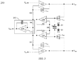
- FIG. 3 is a schematic diagram illustrating an amplifier circuit according to the second embodiment of the present application.
- FIG. 4 is a schematic diagram illustrating the switch configuration of the amplifier circuit in a normal phase according to the third embodiment of the present application.
- FIG. 5 is a schematic diagram illustrating the switch configuration of the amplifier circuit in a fast charge/discharge phase according to the third embodiment of the present application.
- first and the second features are formed in direct contact
- additional features may be formed between the first and the second features, such that the first and the second features may not be in direct contact
- present disclosure may repeat reference numerals and/or letters in the various examples. This repetition is for the purpose of simplicity and clarity and does not in itself dictate a relationship between the various embodiments and/or configurations discussed.
- spatially relative terms such as “beneath, " “below, “ “lower, “ “above, “ “upper, “ and the like, may be used herein for the ease of the description to describe one element or feature's relationship with respect to another element(s) or feature(s) as illustrated in the drawings.
- the spatially relative terms are intended to encompass different orientations of the device in use or operation in addition to the orientation depicted in the figures.
- the apparatus may be otherwise oriented (e.g., rotated by 90 degrees or at other orientations) and the spatially relative descriptors used herein may likewise be interpreted accordingly.
- the electrocardiogram signal of the human body is emitted by the heart, and this electrocardiogram signal can be obtained by measuring the voltage difference between any two endpoints of the human body using the two electrodes of the electrocardiograph (ECG).
- ECG electrocardiograph
- the amplifier circuit in the ECG is used to amplify the voltage difference between said any two endpoints.
- the conventional amplifier circuit has the problem of not being able to completely eliminate the common-mode signal, and the difference between said two electrodes or the ion concentration difference between said any two endpoints may result in different polarization voltages at the two endpoints, thereby causing the presence of the DC offset in the differential-mode signal, which in turns limits the magnification of the ECG.
- the amplifier circuit according to the present application can inhibit the common-mode input signal within the target frequency band and amplify the differential-mode input signal within the target frequency band, thereby increasing the common-mode rejection ratio (CMRR) in the target frequency band. Also, the amplifier circuit according to the present application can be applied in various settings, such as an ECG.
- CMRR common-mode rejection ratio
- FIG. 1 is a schematic diagram illustrating the amplifier circuit according to the first embodiment of the present application.
- the amplifier circuit 100 is configured to generates a positive output signal V OP and a negative output signal V ON according to a positive input signal V IP and a negative input signal V IN , wherein the positive input signal V IP and the negative input signal V IN have a corresponding input differential-mode voltage V ID and input common-mode voltage Vic, and the positive output signal V OP and the negative output signal V ON have a corresponding output differential-mode voltage V OD and output common-mode voltage Voc.
- the amplifier circuit 100 obtains the positive input signal V IP and the negative input signal V IN from any two points of the human body by using electrodes.
- the amplifier circuit 100 includes am amplifying unit 120 and an attenuation unit 130, the amplifying unit 120 is configured to receive the positive input signal V IP and the negative input signal V IN and generate the positive output signal V OP and the negative output signal V ON .
- the function of the amplifying unit 120 is to provide a gain for amplifying the positive input signal V IP and the negative input signal V IN
- the function of the attenuation unit 130 is to attenuate the positive input signal V IP and the negative input signal V IN .
- FIG. 2 is a schematic diagram showing the frequency response of the amplifier circuit 100.
- the horizontal axis indicates the frequency and the vertical axis indicates the gain;
- the broken line represents the differential-mode gain A D of the amplifier circuit 100 with respect to the input differential-mode voltage V ID , whereas the solid line is the common-mode gain A C of the amplifier circuit 100 with respect to the input common-mode voltage V IC .
- the common-mode gain A C above the first specific frequency F 1 (around the high-pass 3dB frequency of the common-mode gain A C ) is kept at a specific gain of greater than 1, whereas the common-mode gain Ac below the first specific frequency F 1 is attenuated.
- the differential-mode gain A D above the second specific frequency F 2 (around the high-pass 3dB frequency of the differential-mode gain A D ) is kept at a specific gain of greater than 1, whereas the differential-mode gain A D below the second specific frequency F 2 is attenuated.
- the first specific frequency F 1 is greater than the second specific frequency F 2 .
- the common-mode gain A C within the range of the target frequency band F 2 to F S is much smaller than the differential-mode gain A D , so as to attain the purpose of increasing the CMRR of the target frequency band F 2 to F S , wherein the F S is the upper limit of the target frequency band.
- the common-mode gain Ac above the first specific frequency F 1 and the differential-mode gain A D above the second specific frequency F 2 are the same (i.e., both equal to the specific gain), yet the present application is not limited thereto; the common-mode gain Ac above the first specific frequency F 1 and the differential-mode gain A D above the second specific frequency F 2 may not be the same.
- the amplifier circuit 100 can filter out the DC offset carried by the input differential-mode voltage V ID , thereby preventing the amplifier circuit 100 from getting saturated as a result of the DC offset.
- the amplifying unit 120 includes a first transconductance amplifier 104, a first operational amplifier 102, a first resistor 101, a second transconductance amplifier 114, a second operational amplifier 112, and a second resistor 111.
- the transconductance of the first transconductance amplifier 104 is Gm F
- the first transconductance amplifier 104 has a positive (+) terminal, a negative (-) terminal, and an output terminal, wherein negative terminal is coupled to first reference voltage V CM .
- the first operational amplifier 102 has a positive (+) terminal, a negative (-) terminal, and an output terminal, the positive terminal of the first operational amplifier 102 receives the positive input signal V IP , the negative terminal of the first operational amplifier 102 is coupled to the output terminal of the first transconductance amplifier 104, and the output terminal of the first operational amplifier 102 outputs the positive output signal V OP and is coupled to the positive terminal of the first transconductance amplifier 104 and the attenuation unit 130.
- the first resistor 101 has a resistance R G , wherein one end of the first resistor 101 is coupled to the negative terminal of the first operational amplifier 102, and the other end of the first resistor 101 is coupled to the attenuation unit 130.
- the second transconductance amplifier 114, the second operational amplifier 112 and the second resistor 111 are arranged symmetrically with respect to the first transconductance amplifier 104, the first operational amplifier 102 and the first resistor 101.
- the transconductance of the second transconductance amplifier 114 is Gm F , which is the same as the transconductance of the first transconductance amplifier 104.
- the second transconductance amplifier 114 has a positive (+) terminal, a negative (-) terminal, and an output terminal
- the second operational amplifier 112 has a positive (+) terminal, a negative (-) terminal, and an output terminal, wherein the positive terminal of the second operational amplifier 112 receives the negative input signal V IN , the negative terminal of the second operational amplifier 112 is coupled to the output terminal of the second transconductance amplifier 114, and the output terminal of the second operational amplifier 112 outputs the negative output signal V IN and is coupled to the positive terminal of the second transconductance amplifier 114 and the attenuation unit 130.
- the second resistor 111 has a resistance R G , which is the same as the resistance of the first resistor 101, one end of the second resistor 111 is coupled to the negative terminal of the second operational amplifier 112, and the other end of the second resistor 111 is coupled to the attenuation unit 130.
- the differential-mode gain A D above the second specific frequency F 2 (around the high-pass 3dB frequency of the differential-mode gain A D ) is kept at a specific gain of 1/(Gm F ⁇ R G ).
- the properties of the first transconductance amplifier 104, the second transconductance amplifier 114, the first resistor 101 and the second resistor 111 can be used to determine the differential-mode gain A D above the second specific frequency F 2 .
- the attenuation unit 130 includes a third transconductance amplifier 108, a positive common-mode capacitor 107, a third operational amplifier 106, a third resistor 105, a fourth transconductance amplifier 118, a negative common-mode capacitor 117, a fourth operational amplifier 116, a fourth resistor 115, a differential-mode capacitor 110 and a fifth resistor 109.
- the transconductance of the third transconductance amplifier 108 is Gm c , the third transconductance amplifier 108 has a positive (+) terminal, a negative (-) terminal, and an output terminal, wherein the negative output signal V OP is fed in from the positive terminal of the third transconductance amplifier 108, the negative terminal of the third transconductance amplifier 108 is coupled to first reference voltage V CM , and the output terminal of the third transconductance amplifier 108 is coupled to the positive common-mode capacitor 107 and the differential-mode capacitor 110.
- the transconductance of the fourth transconductance amplifier 118 is Gm c , which is the same as the transconductance of the third transconductance amplifier 108, and the fourth transconductance amplifier 118 has a positive (+) terminal, a negative (-) terminal, and an output terminal, wherein the negative output signal V ON is fed in from the positive terminal of the fourth transconductance amplifier 118, the negative terminal of the fourth transconductance amplifier 118 is coupled to the first reference voltage V CM , and the output terminal of the fourth transconductance amplifier 118 is coupled to the negative common-mode capacitor 117 and the differential-mode capacitor 110.
- the positive common-mode capacitor 107 and the negative common-mode capacitor 117 have the same first capacitance C 1
- the differential-mode capacitor 110 has a second capacitance C 2 , wherein the second capacitance C 2 is much greater than the first capacitance C 1 . Since for the input common-mode voltage V IC , the differential-mode capacitor 110 can be considered as an open circuit, the attenuation of the input common-mode voltage V IC below the first specific frequency F 1 is mainly subject to the effect from the positive common-mode capacitor 107 and the negative common-mode capacitor 117.
- the positive common-mode capacitor 107 is coupled between the output terminal of the third transconductance amplifier 108 and a second reference voltage
- the negative common-mode capacitor 117 is coupled between the output terminal of the fourth transconductance amplifier 118 and the second reference voltage, wherein the second reference voltage is smaller than the first reference voltage V CM , in the present embodiment, the second reference voltage is the ground voltage.
- the positive common-mode capacitor 107 and the negative common-mode capacitor 117 are configured to attenuate the common-mode gain Ac below the first specific frequency F 1 .
- the differential-mode capacitor 110 is coupled between the output terminal of the third transconductance amplifier 108 and the output terminal of the fourth transconductance amplifier 118.
- the differential-mode capacitor 110 is configured to attenuate the differential-mode gain A D below the second specific frequency F 2 . Since the second capacitance C 2 is much greater than the first capacitance C 1 , the second specific frequency F 2 is lower than the second specific frequency F 2 .
- the common-mode gain Ac of the input common-mode voltage V IC below the first specific frequency F 1 is 2 ⁇ ⁇ f ⁇ C 1 /Gm C , wherein f is the frequency; therefore, the lower the frequency is, the smaller the common-mode gain Ac is.
- the properties of the positive common-mode capacitor 107, the negative common-mode capacitor 117 and the fourth transconductance amplifier 118 can be used to determine the common-mode gain Ac of the input common-mode voltage V IC below the first specific frequency F 1 .
- the CMRR between the second specific frequency F 2 and the first specific frequency F 1 is the differential-mode gain A D above the second specific frequency F 2 (around the high-pass 3dB frequency of the differential-mode gain A D )/the common-mode gain Ac of the input common-mode voltage V IC below the first specific frequency F 1 ; that is, Gm C /(Gm F ⁇ R G ⁇ 2 ⁇ ⁇ f ⁇ C 1 ).
- the third operational amplifier 106 has a positive (+) terminal, a negative (-) terminal, and an output terminal, wherein the positive of the third operational amplifier 106 is coupled to the output terminal of the third transconductance amplifier 108, and the output terminal of the third operational amplifier 106 is coupled to the first resistor 101 of the amplifying unit 120.
- the fourth operational amplifier 116 has a positive (+) terminal, a negative (-) terminal, and an output terminal, the positive terminal of the fourth operational amplifier 116 is coupled to the output terminal of the fourth transconductance amplifier 118, and the output terminal of the fourth operational amplifier 116 is coupled to the second resistor 111 of the amplifying unit 120.
- the third resistor 105 is coupled between the negative terminal and the output terminal of the third operational amplifier 106; the fourth resistor 115 is coupled between the negative terminal and the output terminal of the fourth operational amplifier 116.
- the fifth resistor 109 is coupled between the negative terminal of the third operational amplifier 106 and the negative terminal of the fourth operational amplifier 116.
- the third resistor 105 has a resistance R B , which is the same as the resistance of the fourth resistor 115, and the fifth resistor 109 has a resistance R A .
- the high-pass 3dB frequency of the differential-mode gain A D is ((1+2 ⁇ R B /R A ) ⁇ Gm C ) /(Gm F ⁇ R G ⁇ 4 ⁇ ⁇ C 2 ).
- the properties of the third resistor 105, the fourth resistor 115, the fifth resistor 109, the third transconductance amplifier 108, the second transconductance amplifier 114, the first resistor 101, the second resistor 111 and the differential-mode capacitor 110 can be used to determine the high-pass 3dB frequency of the differential-mode gain A D .
- FIG. 3 is a schematic diagram illustrating an amplifier circuit according to the second embodiment of the present application; the difference between the amplifier circuits in FIG. 3 and FIG. 1 lies in that the amplifier circuit 200 in FIG. 3 , compare with the amplifier circuit 100 in FIG. 1 , further includes a common-mode signal feedback unit 202, which is configured to extract the common-mode voltage feedback signal V RLD from the input common-mode voltage V IC and feed it back into the source object of the positive input signal V IP and the negative input signal V IN .
- a common-mode signal feedback unit 202 which is configured to extract the common-mode voltage feedback signal V RLD from the input common-mode voltage V IC and feed it back into the source object of the positive input signal V IP and the negative input signal V IN .
- the amplifier circuit 100 when the amplifier circuit 100 is used as the ECG, the amplifier circuit 100 obtains the positive input signal V IP and the negative input signal V IN from any two points of the human body using electrodes, and it also feeds the common-mode voltage feedback signal V RLD back to the human body via an electrode at another location of the human body, so as to decrease the input common-mode voltage V IC , thereby avoiding the amplifier circuit 200 from getting saturated.
- the common-mode signal feedback unit 202 is coupled between the output terminal of the third operational amplifier 106 and the output terminal of the fourth operational amplifier 116, and can be implemented using a low-pass filter or integrator.
- the third operational amplifier 106 includes a fifth operational amplifier 204, wherein the fifth operational amplifier 204 has a positive (+) terminal, a negative (-) terminal, and an output terminal.
- the positive terminal of the fifth operational amplifier 204 is coupled to a first reference voltage V CM
- the negative terminal of the fifth operational amplifier 204 are respectively coupled to the output terminal of the third operational amplifier 106 and the output terminal of the fourth operational amplifier 116 via a sixth resistor 103 and a seventh resistor 113
- the negative terminal of the fifth operational amplifier 204 is further coupled to the output terminal of the fifth operational amplifier 204 and the output common-mode voltage feedback signal V RLD via the integral capacitor 206.
- the common-mode signal feedback unit 202 obtains the common-mode voltage feedback signal V RLD that is stably associated with the input common-mode voltage V IC by performing the low-pass filtering process on the voltage between the sixth resistor 103 and the seventh resistor 113 (e.g., by an integration process).
- the common-mode voltage feedback signal V RLD it is not necessary for the common-mode voltage feedback signal V RLD to accurately remove the input common-mode voltage V IC ; rather, the common mode rejection ability of the amplifier circuit 200 can be effectively increased by roughly removing a portion of the input common-mode voltage V IC .
- FIG. 4 and FIG. 5 are schematic diagrams illustrating amplifier circuits according to the third embodiment of the present application.
- the amplifier circuits in FIG. 4 and FIG. 5 differ from that in FIG. 1 in that the amplifier circuits 300A and 300B shown in FIG. 4 and FIG. 5 , compared to the amplifier circuit 100 shown in FIG. 1 , further include a first switch 304, a second switch 314, a third switch 306, a fourth switch 316, a fifth switch 302 and a sixth switch 312; these switches are configured to provide a fast charge/discharge path to the differential-mode capacitor 110 when the DC offset in input differential-mode voltage V ID changes abruptly, so as to speed up the operation time of the amplifier circuits 300A and 300B.
- the amplifier circuits 300A and 300B represent the switch configuration of the amplifier circuit under a normal phase and a fast charge/discharge phase.
- the first switch 304 and the second switch 314 are disposed in the amplifying unit 320
- the third switch 306, the fourth switch 316, the fifth switch 302 and the sixth switch 312 are disposed in the attenuation unit 330.
- the DC offset carried by the input differential-mode voltage V ID may be amplified immediately so that the positive output signal VOP and the negative output signal VON are saturated; the amplifier circuit of the present application can change the configuration shown in the amplifier circuit 300A into the configuration shown in amplifier circuit 300B immediately; that is, the first switch 304, the second switch 314, the third switch 306 and the fourth switch 316 are conducted, and the fifth switch 302 and the sixth switch 312 are disconnected, so as to perform the fast charge or discharge according to the difference between the DC offset carried by the input differential-mode voltage VID and the differential-mode capacitor 110.
- the configuration shown in the amplifier circuit 300B can be changed into the configuration shown in the amplifier circuit 300A; that is, the first switch 304, the second switch 314, the third switch 306 and the fourth switch 316 are disconnected, and the fifth switch 302 and the sixth switch 312 are conducted; since the size of the differential-mode capacitor 110 is greater, the lengthy charge or discharge time can be skipped.
- the drawings do not show circuits configured to control the first switch 304, the second switch 314, the third switch 306, the fourth switch 316, the fifth switch 302 and the sixth switch 312 according to whether the positive output signal VOP and the negative output signal VON are saturated, as well as the circuits configured to change the configuration from the configuration shown in the amplifier circuit 300B to that shown in the amplifier circuit 300A according to a pre-determined time; however, the persons having ordinary skill in the art can understand the implementations of such circuits in light of the foregoing description; therefore, any means that can achieve a similar result are within the scope of the present application.
- the above-mentioned amplifier circuit 200 and amplifier circuits 300A/300B can be implemented individually or in combination, and the present application is not limited thereto.
- the present application can be applied in daily electronic devices other than the ECG; for example, it could be used in a smart watch or wrist band, and could be expanded to any systems that require the amplification of the differential input signal.
- the present application also provides a chip, which includes the amplifier circuit 100/200/300A/300B.
- the present application embodiment improves conventional amplifier circuits, so that it can eliminate most of the common-mode signal using the common-mode gain Ac in the attenuation unit 330 before the back-end subtraction circuit of the amplifier circuit.
- the properties of the differential-mode gain A D of the attenuation unit 330 can be used to improve the issue that the polarization voltage results in the DC offset in the differential-mode signal, so as increase the amplification magnitude of the amplifier circuit to the differential-mode signal.
Landscapes
- Engineering & Computer Science (AREA)
- Power Engineering (AREA)
- Health & Medical Sciences (AREA)
- Life Sciences & Earth Sciences (AREA)
- Biomedical Technology (AREA)
- Molecular Biology (AREA)
- Biophysics (AREA)
- Pathology (AREA)
- Microelectronics & Electronic Packaging (AREA)
- Heart & Thoracic Surgery (AREA)
- Medical Informatics (AREA)
- Physics & Mathematics (AREA)
- Surgery (AREA)
- Animal Behavior & Ethology (AREA)
- General Health & Medical Sciences (AREA)
- Public Health (AREA)
- Veterinary Medicine (AREA)
- Cardiology (AREA)
- Amplifiers (AREA)
Abstract
Description
- The present application relates to an amplifier circuit, chip and electronic device; in particular, an amplifier circuit, chip and electronic device capable of attenuating a common-mode input signal.
- Conventional amplifier circuit has a fixed differential-mode signal gain, whereas the common-mode signal gain is fixed at the unit gain. Therefore, the common-mode signal must be removed by the back-end subtraction circuit, if there is a slight mismatch between the positive terminal and negative terminal of the amplifier circuit, the common-mode signal cannot be removed completely. Additionally, the common-mode signal would occupy part of the voltage range, which makes the amplifier circuit saturated more easily; once the amplifier circuit gets saturated, using the subtraction circuit cannot obtain an amplified differential-mode signal. Moreover, if the differential-mode signal has the direct current (DC) offset, it also makes the amplifier circuit saturated more easily. In view of the foregoing, how to address the above-mentioned issues has become an important task in the related field.
- One purpose of the present application is to disclose an amplifier circuit, chip and electronic device, to address the above-mentioned issue.
- One embodiment of the present application discloses an amplifier circuit, configured to generate a positive output signal and negative output signal according to positive input signal and negative input signal, wherein the positive input signal and the negative input signal has corresponding input differential-mode voltage and input common-mode voltage, the positive output signal and the negative output signal has corresponding output differential-mode voltage and output common-mode voltage, the amplifier circuit includes: amplifying unit, receive the positive input signal and the negative input signal and generates the positive output signal and the negative output signal, the amplifying unit has specific gain; and attenuation unit, includes: positive common-mode capacitor and negative common-mode capacitor, configured to attenuate the input common-mode voltage below a first specific frequency.
- One embodiment of the present application discloses a chip, including the above-mentioned amplifier circuit.
- One embodiment of the present application discloses an electronic device, including the above-mentioned chip.
- Embodiments of the present application improve the amplifier circuit so as to increase the common-mode rejection ratio (CMRR).
-
FIG. 1 is a schematic diagram illustrating an amplifier circuit according to the first embodiment of the present application. -
FIG. 2 is a schematic diagram showing the frequency response of the amplifier circuit inFIG. 1 . -
FIG. 3 is a schematic diagram illustrating an amplifier circuit according to the second embodiment of the present application. -
FIG. 4 is a schematic diagram illustrating the switch configuration of the amplifier circuit in a normal phase according to the third embodiment of the present application. -
FIG. 5 is a schematic diagram illustrating the switch configuration of the amplifier circuit in a fast charge/discharge phase according to the third embodiment of the present application. - Reference numerals used in the drawings are summarized below:
- 100, 200, 300A, 300B
- Amplifier circuit
- 101
- First resistor
- 102
- First operational amplifier
- 103
- Sixth resistor
- 104
- First transconductance amplifier
- 105
- Third resistor
- 106
- Third operational amplifier
- 107
- Positive common-mode capacitor
- 108
- Third transconductance amplifier
- 109
- Fifth resistor
- 110
- Differential-mode capacitor
- 111
- Second resistor
- 112
- Second operational amplifier
- 113
- Seventh resistor
- 114
- Second transconductance amplifier
- 115
- Fourth resistor
- 116
- Fourth operational amplifier
- 117
- Negative common-mode capacitor
- 118
- Fourth transconductance amplifier
- 120, 320
- Amplifying unit
- 130, 330
- Attenuation unit
- 202
- Common-mode signal feedback unit
- 204
- Fifth operational amplifier
- 206
- Integral capacitor
- 302
- Fifth switch
- 304
- First switch
- 306
- Third switch
- 312
- Sixth switch
- 314
- Second switch
- 316
- Fourth switch
- VIP
- Positive input signal
- VIN
- Negative input signal
- VOP
- Positive output signal
- VON
- Negative output signal
- VCM
- First reference voltage
- AD
- Differential-mode gain
- AC
- Common-mode gain
- F1
- First specific frequency
- F2
- Second specific frequency
- FS
- Target frequency band upper limit
- VRLD
- Common-mode voltage feedback signal
- The following disclosure provides many different embodiments, or examples, for implementing different features of the invention. Specific examples of components and arrangements are described below to simplify the present disclosure. As could be appreciated, these are, of course, merely examples and are not intended to be limiting. For example, the formation of a first feature over or on a second feature in the description that follows may include embodiments in which the first and the second features are formed in direct contact, and may also include embodiments in which additional features may be formed between the first and the second features, such that the first and the second features may not be in direct contact. In addition, the present disclosure may repeat reference numerals and/or letters in the various examples. This repetition is for the purpose of simplicity and clarity and does not in itself dictate a relationship between the various embodiments and/or configurations discussed.
- Further, spatially relative terms, such as "beneath, " "below, " "lower, " "above, " "upper, " and the like, may be used herein for the ease of the description to describe one element or feature's relationship with respect to another element(s) or feature(s) as illustrated in the drawings. The spatially relative terms are intended to encompass different orientations of the device in use or operation in addition to the orientation depicted in the figures. The apparatus may be otherwise oriented (e.g., rotated by 90 degrees or at other orientations) and the spatially relative descriptors used herein may likewise be interpreted accordingly.
- Notwithstanding that the numerical ranges and parameters setting forth the broad scope of the invention are approximations, the numerical values set forth in the specific examples are reported as precisely as possible. Any numerical value, however, inherently contains certain errors necessarily resulting from the standard deviation found in the respective testing measurements. Also, as used herein, the term "about" generally means within 10%, 5%, 1%, or 0.5% of a given value or range. Alternatively, the term "about" means within an acceptable standard error of the mean when considered by one of ordinary skill in the art. As could be appreciated, other than in the operating/working examples, or unless otherwise expressly specified, all of the numerical ranges, amounts, values and percentages such as those for quantities of materials, durations of times, temperatures, operating conditions, ratios of amounts, and the likes thereof disclosed herein should be understood as modified in all instances by the term "about." Accordingly, unless indicated to the contrary, the numerical parameters set forth in the present disclosure and attached claims are approximations that can vary as desired. At the very least, each numerical parameter should at least be construed considering the number of reported significant digits and by applying ordinary rounding techniques. Ranges can be expressed herein as from one endpoint to another endpoint or between two endpoints. All ranges disclosed herein are inclusive of the endpoints unless specified otherwise.
- The electrocardiogram signal of the human body is emitted by the heart, and this electrocardiogram signal can be obtained by measuring the voltage difference between any two endpoints of the human body using the two electrodes of the electrocardiograph (ECG). In general, the amplifier circuit in the ECG is used to amplify the voltage difference between said any two endpoints. Nonetheless, the conventional amplifier circuit has the problem of not being able to completely eliminate the common-mode signal, and the difference between said two electrodes or the ion concentration difference between said any two endpoints may result in different polarization voltages at the two endpoints, thereby causing the presence of the DC offset in the differential-mode signal, which in turns limits the magnification of the ECG.
- The amplifier circuit according to the present application can inhibit the common-mode input signal within the target frequency band and amplify the differential-mode input signal within the target frequency band, thereby increasing the common-mode rejection ratio (CMRR) in the target frequency band. Also, the amplifier circuit according to the present application can be applied in various settings, such as an ECG.
-
FIG. 1 is a schematic diagram illustrating the amplifier circuit according to the first embodiment of the present application. Theamplifier circuit 100 is configured to generates a positive output signal VOP and a negative output signal VON according to a positive input signal VIP and a negative input signal VIN, wherein the positive input signal VIP and the negative input signal VIN have a corresponding input differential-mode voltage VID and input common-mode voltage Vic, and the positive output signal VOP and the negative output signal VON have a corresponding output differential-mode voltage VOD and output common-mode voltage Voc. For example, when theamplifier circuit 100 is applied in the ECG, theamplifier circuit 100 obtains the positive input signal VIP and the negative input signal VIN from any two points of the human body by using electrodes. Theamplifier circuit 100 includesam amplifying unit 120 and anattenuation unit 130, the amplifyingunit 120 is configured to receive the positive input signal VIP and the negative input signal VIN and generate the positive output signal VOP and the negative output signal VON. The function of the amplifyingunit 120 is to provide a gain for amplifying the positive input signal VIP and the negative input signal VIN, and the function of theattenuation unit 130 is to attenuate the positive input signal VIP and the negative input signal VIN. - Reference is made simultaneously to
FIG. 2 , which is a schematic diagram showing the frequency response of theamplifier circuit 100. InFIG. 2 , the horizontal axis indicates the frequency and the vertical axis indicates the gain; the broken line represents the differential-mode gain AD of theamplifier circuit 100 with respect to the input differential-mode voltage VID, whereas the solid line is the common-mode gain AC of theamplifier circuit 100 with respect to the input common-mode voltage VIC. As could be seen inFIG. 2 , the common-mode gain AC above the first specific frequency F1 (around the high-pass 3dB frequency of the common-mode gain AC) is kept at a specific gain of greater than 1, whereas the common-mode gain Ac below the first specific frequency F1 is attenuated. The differential-mode gain AD above the second specific frequency F2 (around the high-pass 3dB frequency of the differential-mode gain AD) is kept at a specific gain of greater than 1, whereas the differential-mode gain AD below the second specific frequency F2 is attenuated. The first specific frequency F1 is greater than the second specific frequency F2. Hence, the common-mode gain AC within the range of the target frequency band F2 to FS is much smaller than the differential-mode gain AD, so as to attain the purpose of increasing the CMRR of the target frequency band F2 to FS, wherein the FS is the upper limit of the target frequency band. It should be noted that in the present embodiment, the common-mode gain Ac above the first specific frequency F1 and the differential-mode gain AD above the second specific frequency F2 are the same (i.e., both equal to the specific gain), yet the present application is not limited thereto; the common-mode gain Ac above the first specific frequency F1 and the differential-mode gain AD above the second specific frequency F2 may not be the same. - Moreover, as discussed above, since as the frequency of the differential-mode gain AD below the second specific frequency F2 decreases, the extent of the attenuation increases; that is, the DC component within the differential-mode voltage VID would be attenuated greatly; therefore, the
amplifier circuit 100 can filter out the DC offset carried by the input differential-mode voltage VID, thereby preventing theamplifier circuit 100 from getting saturated as a result of the DC offset. - Returning back to
FIG. 1 ; the amplifyingunit 120 includes afirst transconductance amplifier 104, a firstoperational amplifier 102, afirst resistor 101, asecond transconductance amplifier 114, a secondoperational amplifier 112, and asecond resistor 111. The transconductance of thefirst transconductance amplifier 104 is GmF, and thefirst transconductance amplifier 104 has a positive (+) terminal, a negative (-) terminal, and an output terminal, wherein negative terminal is coupled to first reference voltage VCM. The firstoperational amplifier 102 has a positive (+) terminal, a negative (-) terminal, and an output terminal, the positive terminal of the firstoperational amplifier 102 receives the positive input signal VIP, the negative terminal of the firstoperational amplifier 102 is coupled to the output terminal of thefirst transconductance amplifier 104, and the output terminal of the firstoperational amplifier 102 outputs the positive output signal VOP and is coupled to the positive terminal of thefirst transconductance amplifier 104 and theattenuation unit 130. Thefirst resistor 101 has a resistance RG, wherein one end of thefirst resistor 101 is coupled to the negative terminal of the firstoperational amplifier 102, and the other end of thefirst resistor 101 is coupled to theattenuation unit 130. - The
second transconductance amplifier 114, the secondoperational amplifier 112 and thesecond resistor 111 are arranged symmetrically with respect to thefirst transconductance amplifier 104, the firstoperational amplifier 102 and thefirst resistor 101. The transconductance of thesecond transconductance amplifier 114 is GmF, which is the same as the transconductance of thefirst transconductance amplifier 104. Thesecond transconductance amplifier 114 has a positive (+) terminal, a negative (-) terminal, and an output terminal, and the secondoperational amplifier 112 has a positive (+) terminal, a negative (-) terminal, and an output terminal, wherein the positive terminal of the secondoperational amplifier 112 receives the negative input signal VIN, the negative terminal of the secondoperational amplifier 112 is coupled to the output terminal of thesecond transconductance amplifier 114, and the output terminal of the secondoperational amplifier 112 outputs the negative output signal VIN and is coupled to the positive terminal of thesecond transconductance amplifier 114 and theattenuation unit 130. Thesecond resistor 111 has a resistance RG, which is the same as the resistance of thefirst resistor 101, one end of thesecond resistor 111 is coupled to the negative terminal of the secondoperational amplifier 112, and the other end of thesecond resistor 111 is coupled to theattenuation unit 130. - Specifically, the differential-mode gain AD above the second specific frequency F2 (around the high-pass 3dB frequency of the differential-mode gain AD) is kept at a specific gain of 1/(GmF ∗RG). In other words, the properties of the
first transconductance amplifier 104, thesecond transconductance amplifier 114, thefirst resistor 101 and thesecond resistor 111 can be used to determine the differential-mode gain AD above the second specific frequency F2. - The
attenuation unit 130 includes athird transconductance amplifier 108, a positive common-mode capacitor 107, a thirdoperational amplifier 106, athird resistor 105, afourth transconductance amplifier 118, a negative common-mode capacitor 117, a fourthoperational amplifier 116, afourth resistor 115, a differential-mode capacitor 110 and afifth resistor 109. The transconductance of thethird transconductance amplifier 108 is Gmc, thethird transconductance amplifier 108 has a positive (+) terminal, a negative (-) terminal, and an output terminal, wherein the negative output signal VOP is fed in from the positive terminal of thethird transconductance amplifier 108, the negative terminal of thethird transconductance amplifier 108 is coupled to first reference voltage VCM, and the output terminal of thethird transconductance amplifier 108 is coupled to the positive common-mode capacitor 107 and the differential-mode capacitor 110. The transconductance of thefourth transconductance amplifier 118 is Gmc, which is the same as the transconductance of thethird transconductance amplifier 108, and thefourth transconductance amplifier 118 has a positive (+) terminal, a negative (-) terminal, and an output terminal, wherein the negative output signal VON is fed in from the positive terminal of thefourth transconductance amplifier 118, the negative terminal of thefourth transconductance amplifier 118 is coupled to the first reference voltage VCM, and the output terminal of thefourth transconductance amplifier 118 is coupled to the negative common-mode capacitor 117 and the differential-mode capacitor 110. - The positive common-
mode capacitor 107 and the negative common-mode capacitor 117 have the same first capacitance C1, and the differential-mode capacitor 110 has a second capacitance C2, wherein the second capacitance C2 is much greater than the first capacitance C1. Since for the input common-mode voltage VIC, the differential-mode capacitor 110 can be considered as an open circuit, the attenuation of the input common-mode voltage VIC below the first specific frequency F1 is mainly subject to the effect from the positive common-mode capacitor 107 and the negative common-mode capacitor 117. The positive common-mode capacitor 107 is coupled between the output terminal of thethird transconductance amplifier 108 and a second reference voltage, and the negative common-mode capacitor 117 is coupled between the output terminal of thefourth transconductance amplifier 118 and the second reference voltage, wherein the second reference voltage is smaller than the first reference voltage VCM, in the present embodiment, the second reference voltage is the ground voltage. In other words, the positive common-mode capacitor 107 and the negative common-mode capacitor 117 are configured to attenuate the common-mode gain Ac below the first specific frequency F1. - The differential-mode capacitor 110 is coupled between the output terminal of the
third transconductance amplifier 108 and the output terminal of thefourth transconductance amplifier 118. For the input differential-mode voltage VID, since the second capacitance C2 is much greater than the first capacitance C1, the attenuation of the input differential-mode voltage VID below the second specific frequency F2 is mainly subject to the effect from the differential-mode capacitor 110. In other words, the differential-mode capacitor 110 is configured to attenuate the differential-mode gain AD below the second specific frequency F2. Since the second capacitance C2 is much greater than the first capacitance C1, the second specific frequency F2 is lower than the second specific frequency F2. - Specifically, the common-mode gain Ac of the input common-mode voltage VIC below the first specific frequency F1 is 2π∗f∗C1/GmC, wherein f is the frequency; therefore, the lower the frequency is, the smaller the common-mode gain Ac is. In other words, the properties of the positive common-
mode capacitor 107, the negative common-mode capacitor 117 and thefourth transconductance amplifier 118 can be used to determine the common-mode gain Ac of the input common-mode voltage VIC below the first specific frequency F1. The CMRR between the second specific frequency F2 and the first specific frequency F1 is the differential-mode gain AD above the second specific frequency F2 (around the high-pass 3dB frequency of the differential-mode gain AD)/the common-mode gain Ac of the input common-mode voltage VIC below the first specific frequency F1; that is, GmC/(GmF ∗RG ∗2π∗f∗C1). - The third
operational amplifier 106 has a positive (+) terminal, a negative (-) terminal, and an output terminal, wherein the positive of the thirdoperational amplifier 106 is coupled to the output terminal of thethird transconductance amplifier 108, and the output terminal of the thirdoperational amplifier 106 is coupled to thefirst resistor 101 of the amplifyingunit 120. The fourthoperational amplifier 116 has a positive (+) terminal, a negative (-) terminal, and an output terminal, the positive terminal of the fourthoperational amplifier 116 is coupled to the output terminal of thefourth transconductance amplifier 118, and the output terminal of the fourthoperational amplifier 116 is coupled to thesecond resistor 111 of the amplifyingunit 120. Thethird resistor 105 is coupled between the negative terminal and the output terminal of the thirdoperational amplifier 106; thefourth resistor 115 is coupled between the negative terminal and the output terminal of the fourthoperational amplifier 116. Thefifth resistor 109 is coupled between the negative terminal of the thirdoperational amplifier 106 and the negative terminal of the fourthoperational amplifier 116. Thethird resistor 105 has a resistance RB, which is the same as the resistance of thefourth resistor 115, and thefifth resistor 109 has a resistance RA. The high-pass 3dB frequency of the differential-mode gain AD is ((1+2∗RB/RA) ∗GmC) /(GmF ∗RG ∗4π∗C2). In other words, the properties of thethird resistor 105, thefourth resistor 115, thefifth resistor 109, thethird transconductance amplifier 108, thesecond transconductance amplifier 114, thefirst resistor 101, thesecond resistor 111 and the differential-mode capacitor 110 can be used to determine the high-pass 3dB frequency of the differential-mode gain AD. -
FIG. 3 is a schematic diagram illustrating an amplifier circuit according to the second embodiment of the present application; the difference between the amplifier circuits inFIG. 3 andFIG. 1 lies in that theamplifier circuit 200 inFIG. 3 , compare with theamplifier circuit 100 inFIG. 1 , further includes a common-modesignal feedback unit 202, which is configured to extract the common-mode voltage feedback signal VRLD from the input common-mode voltage VIC and feed it back into the source object of the positive input signal VIP and the negative input signal VIN. For example, when theamplifier circuit 100 is used as the ECG, theamplifier circuit 100 obtains the positive input signal VIP and the negative input signal VIN from any two points of the human body using electrodes, and it also feeds the common-mode voltage feedback signal VRLD back to the human body via an electrode at another location of the human body, so as to decrease the input common-mode voltage VIC, thereby avoiding theamplifier circuit 200 from getting saturated. The common-modesignal feedback unit 202 is coupled between the output terminal of the thirdoperational amplifier 106 and the output terminal of the fourthoperational amplifier 116, and can be implemented using a low-pass filter or integrator. The common-modesignal feedback unit 202 shown inFIG. 3 includes a fifthoperational amplifier 204, wherein the fifthoperational amplifier 204 has a positive (+) terminal, a negative (-) terminal, and an output terminal. The positive terminal of the fifthoperational amplifier 204 is coupled to a first reference voltage VCM, the negative terminal of the fifthoperational amplifier 204 are respectively coupled to the output terminal of the thirdoperational amplifier 106 and the output terminal of the fourthoperational amplifier 116 via a sixth resistor 103 and a seventh resistor 113, and the negative terminal of the fifthoperational amplifier 204 is further coupled to the output terminal of the fifthoperational amplifier 204 and the output common-mode voltage feedback signal VRLD via theintegral capacitor 206. - Since the voltage between the sixth resistor 103 and the seventh resistor 113 are associated with the input common-mode voltage VIC, the common-mode
signal feedback unit 202 obtains the common-mode voltage feedback signal VRLD that is stably associated with the input common-mode voltage VIC by performing the low-pass filtering process on the voltage between the sixth resistor 103 and the seventh resistor 113 (e.g., by an integration process). In practice, it is not necessary for the common-mode voltage feedback signal VRLD to accurately remove the input common-mode voltage VIC; rather, the common mode rejection ability of theamplifier circuit 200 can be effectively increased by roughly removing a portion of the input common-mode voltage VIC. -
FIG. 4 andFIG. 5 are schematic diagrams illustrating amplifier circuits according to the third embodiment of the present application. The amplifier circuits inFIG. 4 andFIG. 5 differ from that inFIG. 1 in that theamplifier circuits FIG. 4 andFIG. 5 , compared to theamplifier circuit 100 shown inFIG. 1 , further include afirst switch 304, asecond switch 314, athird switch 306, afourth switch 316, afifth switch 302 and asixth switch 312; these switches are configured to provide a fast charge/discharge path to the differential-mode capacitor 110 when the DC offset in input differential-mode voltage VID changes abruptly, so as to speed up the operation time of theamplifier circuits amplifier circuits first switch 304 and thesecond switch 314 are disposed in theamplifying unit 320, and thethird switch 306, thefourth switch 316, thefifth switch 302 and thesixth switch 312 are disposed in theattenuation unit 330. - For example, when the
amplifier circuits amplifier circuit 300A into the configuration shown inamplifier circuit 300B immediately; that is, thefirst switch 304, thesecond switch 314, thethird switch 306 and thefourth switch 316 are conducted, and thefifth switch 302 and thesixth switch 312 are disconnected, so as to perform the fast charge or discharge according to the difference between the DC offset carried by the input differential-mode voltage VID and the differential-mode capacitor 110. After the passage of a pre-determined time, the configuration shown in theamplifier circuit 300B can be changed into the configuration shown in theamplifier circuit 300A; that is, thefirst switch 304, thesecond switch 314, thethird switch 306 and thefourth switch 316 are disconnected, and thefifth switch 302 and thesixth switch 312 are conducted; since the size of the differential-mode capacitor 110 is greater, the lengthy charge or discharge time can be skipped. - It should be noted that, for the sake of brevity, the drawings do not show circuits configured to control the
first switch 304, thesecond switch 314, thethird switch 306, thefourth switch 316, thefifth switch 302 and thesixth switch 312 according to whether the positive output signal VOP and the negative output signal VON are saturated, as well as the circuits configured to change the configuration from the configuration shown in theamplifier circuit 300B to that shown in theamplifier circuit 300A according to a pre-determined time; however, the persons having ordinary skill in the art can understand the implementations of such circuits in light of the foregoing description; therefore, any means that can achieve a similar result are within the scope of the present application. - The above-mentioned
amplifier circuit 200 andamplifier circuits 300A/300B can be implemented individually or in combination, and the present application is not limited thereto. The present application can be applied in daily electronic devices other than the ECG; for example, it could be used in a smart watch or wrist band, and could be expanded to any systems that require the amplification of the differential input signal. The present application also provides a chip, which includes theamplifier circuit 100/200/300A/300B. - The present application embodiment improves conventional amplifier circuits, so that it can eliminate most of the common-mode signal using the common-mode gain Ac in the
attenuation unit 330 before the back-end subtraction circuit of the amplifier circuit. In this way, the properties of the differential-mode gain AD of theattenuation unit 330 can be used to improve the issue that the polarization voltage results in the DC offset in the differential-mode signal, so as increase the amplification magnitude of the amplifier circuit to the differential-mode signal. - The foregoing outlines the features of several embodiments so that those skilled in the art may better understand various aspects of the present disclosure. Those skilled in the art should appreciate that they may readily use the present disclosure as a basis for designing or modifying other processes and structures for carrying out the same purposes and/or achieving the same advantages of embodiments introduced herein. Those skilled in the art should also realize that such equivalent embodiments still fall within the spirit and scope of the present disclosure, and they may make various changes, substitutions, and alterations thereto without departing from the spirit and scope of the present disclosure.
Claims (21)
- An amplifier circuit, configured to generate a positive output signal and a negative output signal according to a positive input signal and a negative input signal, wherein the positive input signal and the negative input signal have a corresponding input differential-mode voltage and input common-mode voltage, and the positive output signal and the negative output signal have a corresponding output differential-mode voltage and output common-mode voltage, characterized in that the amplifier circuit is comprises:an amplifying unit, configured to receive the positive input signal and the negative input signal and generate the positive output signal and the negative output signal, wherein the amplifying unit has a specific gain; andan attenuation unit, comprising:
a positive common-mode capacitor and a negative common-mode capacitor, configured to attenuate the input common-mode voltage below a first specific frequency. - The amplifier circuit of claim 1, wherein the attenuation unit further comprises:
a differential-mode capacitor, configured to attenuate the input differential-mode voltage below a second specific frequency, wherein the first specific frequency is different from the second specific frequency. - The amplifier circuit of claim 2, wherein the amplifying unit comprises:a first transconductance amplifier, having a positive terminal, a negative terminal and an output terminal;a first operational amplifier, having a positive terminal, a negative terminal and an output terminal, wherein the positive terminal of the first operational amplifier receives the positive input signal, the negative terminal of the first operational amplifier is coupled to the output terminal of the first transconductance amplifier, and the output terminal of the first operational amplifier outputs the positive output signal and is coupled to the positive terminal of the first transconductance amplifier;a second transconductance amplifier, having a positive terminal, a negative terminal and an output terminal; anda second operational amplifier, having a positive terminal, a negative terminal and an output terminal, wherein the positive terminal of the second operational amplifier receives the negative input signal, the negative terminal of the second operational amplifier is coupled to the output terminal of the second transconductance amplifier, and the output terminal of the second operational amplifier outputs the negative output signal and is coupled to the positive terminal of the second transconductance amplifier.
- The amplifier circuit of claim 3, wherein the amplifying unit further comprises:a first resistor, coupled between the negative terminal of the first operational amplifier and the attenuation unit; anda second resistor, coupled between the negative terminal of the second operational amplifier and the attenuation unit.
- The amplifier circuit of claim 3, wherein the amplifying unit further comprises:a first switch, coupled between the positive terminal of the first transconductance amplifier and the output terminal of the first transconductance amplifier; anda second switch, coupled between the positive terminal of the second transconductance amplifier and the output terminal of the second transconductance amplifier, wherein when the positive output signal and the negative output signal are saturated, the first switch and the second switch are conducted.
- The amplifier circuit of claim 2, wherein the attenuation unit further comprises:a third transconductance amplifier, having a positive terminal, a negative terminal and an output terminal, wherein the negative output signal is fed in through the positive terminal of the third transconductance amplifier, and the output terminal of the third transconductance amplifier is coupled to the positive common-mode capacitor and the differential-mode capacitor; anda fourth transconductance amplifier, having a positive terminal, a negative terminal and an output terminal, wherein the negative output signal is fed in through the positive terminal of the fourth transconductance amplifier, and the output terminal of the fourth transconductance amplifier is coupled to the negative common-mode capacitor and the differential-mode capacitor.
- The amplifier circuit of claim 6, wherein the differential-mode capacitor is coupled between the output terminal of the third transconductance amplifier and the output terminal of the fourth transconductance amplifier.
- The amplifier circuit of claim 7, wherein the positive common-mode capacitor and the negative common-mode capacitor have the same first capacitance, and the differential-mode capacitor has a second capacitance, wherein the second capacitance is greater than the first capacitance.
- The amplifier circuit of claim 6, wherein the attenuation unit further comprises:a third operational amplifier, having a positive terminal, a negative terminal and an output terminal, wherein the positive terminal of the third operational amplifier is coupled to the output terminal of the third transconductance amplifier, and the output terminal of the third operational amplifier is coupled to the amplifying unit; anda fourth operational amplifier, having a positive terminal, a negative terminal and an output terminal, wherein the positive terminal of the fourth operational amplifier is coupled to the output terminal of the fourth transconductance amplifier, and the output terminal of the fourth operational amplifier is coupled to the amplifying unit.
- The amplifier circuit of claim 9, wherein the attenuation unit further comprises:a third resistor, coupled between the negative terminal of the third operational amplifier and the output terminal; anda fourth resistor, coupled between the negative terminal of the fourth operational amplifier and the output terminal.
- The amplifier circuit of claim 10, wherein the attenuation unit further comprises:
a fifth resistor, coupled between the negative terminal of the third operational amplifier and the negative terminal of the fourth operational amplifier. - The amplifier circuit of claim 9, further comprises:a common-mode signal feedback unit, coupled between the output terminal of the third operational amplifier and the output terminal of the fourth operational amplifier.
- The amplifier circuit of claim 12, wherein the common-mode signal feedback unit comprises a low-pass filter or an integrator.
- The amplifier circuit of claim 6, wherein the attenuation unit further comprises:a third switch, coupled between the positive terminal of the third transconductance amplifier and the output terminal of the third transconductance amplifier; anda fourth switch, coupled between the fourth transconductance amplifier the positive terminal of the positive and the output terminal of the fourth transconductance amplifier, wherein when the positive output signal and the negative output signal are saturated, the first switch and the second switch are conducted.
- The amplifier circuit of claim 9, wherein the attenuation unit further comprises:a fifth switch, coupled between the output terminal of the third operational amplifier and the amplifying unit; anda sixth switch, coupled between the output terminal of the fourth operational amplifier and the amplifying unit, wherein when the positive output signal and the negative output signal are saturated, the fifth switch and the sixth switch are not conducted.
- The amplifier circuit of any of claims 2 to 15, wherein the first specific frequency is greater than the second specific frequency.
- The amplifier circuit of claim 16, wherein the amplifying unit provides the specific gain to the input common-mode voltage above the first specific frequency.
- The amplifier circuit of claim 17, wherein the amplifying unit provides the specific gain to the input differential-mode voltage above the second specific frequency.
- The amplifier circuit of claim 18, wherein the specific gain of the amplifying unit is greater than 1.
- A chip, characterized by comprising:
the amplifier circuit of any of claims 1-19. - An electronic device, characterized by comprising:
the chip of claim 20.
Applications Claiming Priority (1)
| Application Number | Priority Date | Filing Date | Title |
|---|---|---|---|
| PCT/CN2019/100721 WO2021026860A1 (en) | 2019-08-15 | 2019-08-15 | Amplifier circuit, chip, and electronic apparatus |
Publications (3)
| Publication Number | Publication Date |
|---|---|
| EP3806329A1 true EP3806329A1 (en) | 2021-04-14 |
| EP3806329A4 EP3806329A4 (en) | 2021-08-25 |
| EP3806329B1 EP3806329B1 (en) | 2023-07-19 |
Family
ID=68927578
Family Applications (1)
| Application Number | Title | Priority Date | Filing Date |
|---|---|---|---|
| EP19930187.0A Active EP3806329B1 (en) | 2019-08-15 | 2019-08-15 | Amplifier circuit, chip, and electronic apparatus |
Country Status (5)
| Country | Link |
|---|---|
| US (1) | US11575357B2 (en) |
| EP (1) | EP3806329B1 (en) |
| KR (1) | KR102472150B1 (en) |
| CN (2) | CN110622413B (en) |
| WO (1) | WO2021026860A1 (en) |
Families Citing this family (7)
| Publication number | Priority date | Publication date | Assignee | Title |
|---|---|---|---|---|
| CN113110188B (en) * | 2021-04-21 | 2022-06-17 | 广州金升阳科技有限公司 | CAN bus receiving circuit |
| CN114236221B (en) * | 2021-10-13 | 2023-09-26 | 北京华峰测控技术股份有限公司 | Differential voltage measurement circuit, device and method |
| CN114660525B (en) * | 2022-02-22 | 2025-06-03 | 许继集团有限公司 | A CT secondary circuit disconnection detection device and method |
| TWI790966B (en) * | 2022-05-10 | 2023-01-21 | 茂達電子股份有限公司 | Switching charger for supplying stable power |
| CN114978073B (en) * | 2022-05-18 | 2026-02-24 | 深圳先进技术研究院 | Amplifying circuit, detecting chip and wearable device |
| US12603617B2 (en) * | 2023-10-11 | 2026-04-14 | Realtek Semiconductor Corp. | High accuracy low noise voltage delivery network and method thereof |
| CN118095173A (en) * | 2024-04-29 | 2024-05-28 | 崂山国家实验室 | Analog signal amplification device and method |
Family Cites Families (19)
| Publication number | Priority date | Publication date | Assignee | Title |
|---|---|---|---|---|
| US4320351A (en) * | 1980-02-25 | 1982-03-16 | Sri International | Differential amplifying system with bootstrapping |
| US5206602A (en) * | 1992-04-30 | 1993-04-27 | Hewlett-Packard Company | Biomedical amplifier circuit |
| DE60141984D1 (en) | 2000-08-03 | 2010-06-10 | Broadcom Corp | EQUAL TOUCH CHANGE WITH SWITCHED CAPACITIES FOR A SUM STREAM-FREE DIFFERENTIAL AMPLIFIER |
| JP4156573B2 (en) * | 2004-08-03 | 2008-09-24 | 日本電信電話株式会社 | Transimpedance amplifier |
| CN100594671C (en) * | 2006-08-25 | 2010-03-17 | 王悦 | Prepositive differential amplifier and method for expanding its input range |
| CN101966080B (en) * | 2010-10-26 | 2012-06-20 | 东北大学 | Portable active electroencephalogram monitor and control method thereof |
| CN102570989B (en) * | 2010-12-27 | 2016-08-10 | 无锡华润上华半导体有限公司 | Operational amplification circuit |
| US9263995B2 (en) * | 2012-11-14 | 2016-02-16 | Mediatek Inc. | Multi-mode OPAMP-based circuit |
| WO2014123593A1 (en) * | 2013-02-07 | 2014-08-14 | The Boeing Company | Flight deck lighting for information display |
| US10177781B2 (en) * | 2013-06-24 | 2019-01-08 | Silicon Laboratories Inc. | Circuit including a switched capacitor bridge and method |
| EP2819306B1 (en) * | 2013-06-27 | 2016-04-06 | Imec | Instrumentation amplifier and signal amplification method |
| CN203457116U (en) * | 2013-07-31 | 2014-02-26 | 快捷半导体(苏州)有限公司 | CMFB differential amplification circuit and integrated circuit |
| CN104467713A (en) * | 2013-09-18 | 2015-03-25 | 成都英力拓信息技术有限公司 | Pre-amplification circuit with high common mode rejection ratio for biological myoelectricity data acquisition system |
| CN103705230B (en) * | 2014-01-14 | 2017-02-15 | 南京大学 | Pre-stage circuit in bioelectricity detection |
| CN104883047A (en) * | 2014-12-29 | 2015-09-02 | 余姚亿威电子科技有限公司 | Common-mode and differential-mode current suppression circuit |
| CN107104648B (en) * | 2016-02-19 | 2019-12-17 | 深圳市汇顶科技股份有限公司 | amplifying circuit |
| CN107171650B (en) * | 2016-03-08 | 2020-04-17 | 晶豪科技股份有限公司 | Variable gain amplifier circuit |
| CN107689735B (en) * | 2016-08-05 | 2020-01-31 | 台达电子企业管理(上海)有限公司 | Power conversion system and common-mode voltage suppression method thereof |
| EP3422569B1 (en) * | 2017-06-30 | 2021-11-10 | Nxp B.V. | An amplifier circuit |
-
2019
- 2019-08-15 EP EP19930187.0A patent/EP3806329B1/en active Active
- 2019-08-15 CN CN201980001623.1A patent/CN110622413B/en active Active
- 2019-08-15 KR KR1020207036270A patent/KR102472150B1/en active Active
- 2019-08-15 CN CN202110777590.9A patent/CN113659946B/en active Active
- 2019-08-15 WO PCT/CN2019/100721 patent/WO2021026860A1/en not_active Ceased
-
2020
- 2020-12-02 US US17/110,097 patent/US11575357B2/en active Active
Also Published As
| Publication number | Publication date |
|---|---|
| CN113659946A (en) | 2021-11-16 |
| KR20210020919A (en) | 2021-02-24 |
| US20210091735A1 (en) | 2021-03-25 |
| US11575357B2 (en) | 2023-02-07 |
| KR102472150B1 (en) | 2022-11-28 |
| CN113659946B (en) | 2022-09-13 |
| WO2021026860A1 (en) | 2021-02-18 |
| EP3806329A4 (en) | 2021-08-25 |
| CN110622413B (en) | 2021-07-20 |
| CN110622413A (en) | 2019-12-27 |
| EP3806329B1 (en) | 2023-07-19 |
Similar Documents
| Publication | Publication Date | Title |
|---|---|---|
| US11575357B2 (en) | Amplifier circuit, chip and electronic device | |
| EP2819306B1 (en) | Instrumentation amplifier and signal amplification method | |
| US10778165B2 (en) | High dynamic range sensing front-end for neural signal recording systems | |
| US8390374B2 (en) | Apparatus and method for amplification with high front-end gain in the presence of large DC offsets | |
| US11617531B2 (en) | Circuit applied to biopotential acquisition system | |
| CN111682856B (en) | Analog front-end circuit of bioelectric sensor | |
| US9564874B1 (en) | Ultra-low frequency bio-medical active-RC lowpass filters | |
| Lentola et al. | A 1-/spl mu/A front end for pacemaker atrial sensing channels with early sensing capability | |
| US20050107674A1 (en) | DC offset cancellation techniques | |
| Duan et al. | An OTA-C filter for ECG acquisition systems with highly linear range and less passband attenuation | |
| CN104716912A (en) | Small-signal amplification system | |
| US20040155702A1 (en) | Active filter circuit arrangement | |
| Singh et al. | Switched-capacitor filter design for ECG application using 180nm CMOS technology | |
| Qin et al. | A low power analog front-end for portable biopotential acquisition systems | |
| DE102015104910B4 (en) | Device and method for multi-channel auto-zero and chopper amplifiers | |
| CN105305971A (en) | Low-noise preamplifier circuit with reduced input capacitors | |
| KR102685321B1 (en) | Bioelectrical amplifier with tunable bandwidth | |
| Mahmoud et al. | Digitally programmable OTA-C low pass filter for ECG detection systems | |
| CN111342818B (en) | Filters and their methods of operation | |
| Redoute et al. | An instrumentation amplifier input circuit with a high immunity to EMI | |
| Zhao et al. | A High Linearity Large Time Constants Switched-Resistor Filter for Biomedical Applications | |
| El-Attar et al. | A comparative analysis of optimized cmos neural amplifier | |
| JP6053997B1 (en) | Filter device | |
| Moghimi | To chop or Auto-zero: that is the question | |
| Aiello et al. | Design of a neural recording amplifier robust to EMI |
Legal Events
| Date | Code | Title | Description |
|---|---|---|---|
| STAA | Information on the status of an ep patent application or granted ep patent |
Free format text: STATUS: UNKNOWN |
|
| STAA | Information on the status of an ep patent application or granted ep patent |
Free format text: STATUS: THE INTERNATIONAL PUBLICATION HAS BEEN MADE |
|
| PUAI | Public reference made under article 153(3) epc to a published international application that has entered the european phase |
Free format text: ORIGINAL CODE: 0009012 |
|
| STAA | Information on the status of an ep patent application or granted ep patent |
Free format text: STATUS: REQUEST FOR EXAMINATION WAS MADE |
|
| 17P | Request for examination filed |
Effective date: 20201204 |
|
| AK | Designated contracting states |
Kind code of ref document: A1 Designated state(s): AL AT BE BG CH CY CZ DE DK EE ES FI FR GB GR HR HU IE IS IT LI LT LU LV MC MK MT NL NO PL PT RO RS SE SI SK SM TR |
|
| AX | Request for extension of the european patent |
Extension state: BA ME |
|
| A4 | Supplementary search report drawn up and despatched |
Effective date: 20210723 |
|
| RIC1 | Information provided on ipc code assigned before grant |
Ipc: H03F 3/20 20060101AFI20210719BHEP Ipc: A61B 5/00 20060101ALI20210719BHEP Ipc: H03F 3/45 20060101ALI20210719BHEP Ipc: A61B 5/308 20210101ALI20210719BHEP Ipc: H03F 3/213 20060101ALI20210719BHEP |
|
| DAV | Request for validation of the european patent (deleted) | ||
| DAX | Request for extension of the european patent (deleted) | ||
| GRAP | Despatch of communication of intention to grant a patent |
Free format text: ORIGINAL CODE: EPIDOSNIGR1 |
|
| STAA | Information on the status of an ep patent application or granted ep patent |
Free format text: STATUS: GRANT OF PATENT IS INTENDED |
|
| INTG | Intention to grant announced |
Effective date: 20230411 |
|
| GRAS | Grant fee paid |
Free format text: ORIGINAL CODE: EPIDOSNIGR3 |
|
| GRAA | (expected) grant |
Free format text: ORIGINAL CODE: 0009210 |
|
| STAA | Information on the status of an ep patent application or granted ep patent |
Free format text: STATUS: THE PATENT HAS BEEN GRANTED |
|
| AK | Designated contracting states |
Kind code of ref document: B1 Designated state(s): AL AT BE BG CH CY CZ DE DK EE ES FI FR GB GR HR HU IE IS IT LI LT LU LV MC MK MT NL NO PL PT RO RS SE SI SK SM TR |
|
| REG | Reference to a national code |
Ref country code: GB Ref legal event code: FG4D |
|
| REG | Reference to a national code |
Ref country code: CH Ref legal event code: EP |
|
| REG | Reference to a national code |
Ref country code: DE Ref legal event code: R096 Ref document number: 602019033324 Country of ref document: DE |
|
| REG | Reference to a national code |
Ref country code: IE Ref legal event code: FG4D |
|
| REG | Reference to a national code |
Ref country code: LT Ref legal event code: MG9D |
|
| REG | Reference to a national code |
Ref country code: NL Ref legal event code: MP Effective date: 20230719 |
|
| REG | Reference to a national code |
Ref country code: AT Ref legal event code: MK05 Ref document number: 1590497 Country of ref document: AT Kind code of ref document: T Effective date: 20230719 |
|
| PG25 | Lapsed in a contracting state [announced via postgrant information from national office to epo] |
Ref country code: NL Free format text: LAPSE BECAUSE OF FAILURE TO SUBMIT A TRANSLATION OF THE DESCRIPTION OR TO PAY THE FEE WITHIN THE PRESCRIBED TIME-LIMIT Effective date: 20230719 |
|
| PG25 | Lapsed in a contracting state [announced via postgrant information from national office to epo] |
Ref country code: GR Free format text: LAPSE BECAUSE OF FAILURE TO SUBMIT A TRANSLATION OF THE DESCRIPTION OR TO PAY THE FEE WITHIN THE PRESCRIBED TIME-LIMIT Effective date: 20231020 |
|
| PG25 | Lapsed in a contracting state [announced via postgrant information from national office to epo] |
Ref country code: IS Free format text: LAPSE BECAUSE OF FAILURE TO SUBMIT A TRANSLATION OF THE DESCRIPTION OR TO PAY THE FEE WITHIN THE PRESCRIBED TIME-LIMIT Effective date: 20231119 |
|
| PG25 | Lapsed in a contracting state [announced via postgrant information from national office to epo] |
Ref country code: SE Free format text: LAPSE BECAUSE OF FAILURE TO SUBMIT A TRANSLATION OF THE DESCRIPTION OR TO PAY THE FEE WITHIN THE PRESCRIBED TIME-LIMIT Effective date: 20230719 Ref country code: RS Free format text: LAPSE BECAUSE OF FAILURE TO SUBMIT A TRANSLATION OF THE DESCRIPTION OR TO PAY THE FEE WITHIN THE PRESCRIBED TIME-LIMIT Effective date: 20230719 Ref country code: PT Free format text: LAPSE BECAUSE OF FAILURE TO SUBMIT A TRANSLATION OF THE DESCRIPTION OR TO PAY THE FEE WITHIN THE PRESCRIBED TIME-LIMIT Effective date: 20231120 Ref country code: NO Free format text: LAPSE BECAUSE OF FAILURE TO SUBMIT A TRANSLATION OF THE DESCRIPTION OR TO PAY THE FEE WITHIN THE PRESCRIBED TIME-LIMIT Effective date: 20231019 Ref country code: LV Free format text: LAPSE BECAUSE OF FAILURE TO SUBMIT A TRANSLATION OF THE DESCRIPTION OR TO PAY THE FEE WITHIN THE PRESCRIBED TIME-LIMIT Effective date: 20230719 Ref country code: LT Free format text: LAPSE BECAUSE OF FAILURE TO SUBMIT A TRANSLATION OF THE DESCRIPTION OR TO PAY THE FEE WITHIN THE PRESCRIBED TIME-LIMIT Effective date: 20230719 Ref country code: IS Free format text: LAPSE BECAUSE OF FAILURE TO SUBMIT A TRANSLATION OF THE DESCRIPTION OR TO PAY THE FEE WITHIN THE PRESCRIBED TIME-LIMIT Effective date: 20231119 Ref country code: HR Free format text: LAPSE BECAUSE OF FAILURE TO SUBMIT A TRANSLATION OF THE DESCRIPTION OR TO PAY THE FEE WITHIN THE PRESCRIBED TIME-LIMIT Effective date: 20230719 Ref country code: GR Free format text: LAPSE BECAUSE OF FAILURE TO SUBMIT A TRANSLATION OF THE DESCRIPTION OR TO PAY THE FEE WITHIN THE PRESCRIBED TIME-LIMIT Effective date: 20231020 Ref country code: FI Free format text: LAPSE BECAUSE OF FAILURE TO SUBMIT A TRANSLATION OF THE DESCRIPTION OR TO PAY THE FEE WITHIN THE PRESCRIBED TIME-LIMIT Effective date: 20230719 Ref country code: AT Free format text: LAPSE BECAUSE OF FAILURE TO SUBMIT A TRANSLATION OF THE DESCRIPTION OR TO PAY THE FEE WITHIN THE PRESCRIBED TIME-LIMIT Effective date: 20230719 |
|
| PG25 | Lapsed in a contracting state [announced via postgrant information from national office to epo] |
Ref country code: PL Free format text: LAPSE BECAUSE OF FAILURE TO SUBMIT A TRANSLATION OF THE DESCRIPTION OR TO PAY THE FEE WITHIN THE PRESCRIBED TIME-LIMIT Effective date: 20230719 |
|
| REG | Reference to a national code |
Ref country code: CH Ref legal event code: PL |
|
| PG25 | Lapsed in a contracting state [announced via postgrant information from national office to epo] |
Ref country code: LU Free format text: LAPSE BECAUSE OF NON-PAYMENT OF DUE FEES Effective date: 20230815 |
|
| REG | Reference to a national code |
Ref country code: DE Ref legal event code: R097 Ref document number: 602019033324 Country of ref document: DE |
|
| PG25 | Lapsed in a contracting state [announced via postgrant information from national office to epo] |
Ref country code: ES Free format text: LAPSE BECAUSE OF FAILURE TO SUBMIT A TRANSLATION OF THE DESCRIPTION OR TO PAY THE FEE WITHIN THE PRESCRIBED TIME-LIMIT Effective date: 20230719 |
|
| PG25 | Lapsed in a contracting state [announced via postgrant information from national office to epo] |
Ref country code: SM Free format text: LAPSE BECAUSE OF FAILURE TO SUBMIT A TRANSLATION OF THE DESCRIPTION OR TO PAY THE FEE WITHIN THE PRESCRIBED TIME-LIMIT Effective date: 20230719 Ref country code: RO Free format text: LAPSE BECAUSE OF FAILURE TO SUBMIT A TRANSLATION OF THE DESCRIPTION OR TO PAY THE FEE WITHIN THE PRESCRIBED TIME-LIMIT Effective date: 20230719 Ref country code: LU Free format text: LAPSE BECAUSE OF NON-PAYMENT OF DUE FEES Effective date: 20230815 Ref country code: ES Free format text: LAPSE BECAUSE OF FAILURE TO SUBMIT A TRANSLATION OF THE DESCRIPTION OR TO PAY THE FEE WITHIN THE PRESCRIBED TIME-LIMIT Effective date: 20230719 Ref country code: EE Free format text: LAPSE BECAUSE OF FAILURE TO SUBMIT A TRANSLATION OF THE DESCRIPTION OR TO PAY THE FEE WITHIN THE PRESCRIBED TIME-LIMIT Effective date: 20230719 Ref country code: DK Free format text: LAPSE BECAUSE OF FAILURE TO SUBMIT A TRANSLATION OF THE DESCRIPTION OR TO PAY THE FEE WITHIN THE PRESCRIBED TIME-LIMIT Effective date: 20230719 Ref country code: CZ Free format text: LAPSE BECAUSE OF FAILURE TO SUBMIT A TRANSLATION OF THE DESCRIPTION OR TO PAY THE FEE WITHIN THE PRESCRIBED TIME-LIMIT Effective date: 20230719 Ref country code: SK Free format text: LAPSE BECAUSE OF FAILURE TO SUBMIT A TRANSLATION OF THE DESCRIPTION OR TO PAY THE FEE WITHIN THE PRESCRIBED TIME-LIMIT Effective date: 20230719 Ref country code: CH Free format text: LAPSE BECAUSE OF NON-PAYMENT OF DUE FEES Effective date: 20230831 Ref country code: MC Free format text: LAPSE BECAUSE OF FAILURE TO SUBMIT A TRANSLATION OF THE DESCRIPTION OR TO PAY THE FEE WITHIN THE PRESCRIBED TIME-LIMIT Effective date: 20230719 |
|
| REG | Reference to a national code |
Ref country code: BE Ref legal event code: MM Effective date: 20230831 |
|
| REG | Reference to a national code |
Ref country code: IE Ref legal event code: MM4A |
|
| PLBE | No opposition filed within time limit |
Free format text: ORIGINAL CODE: 0009261 |
|
| STAA | Information on the status of an ep patent application or granted ep patent |
Free format text: STATUS: NO OPPOSITION FILED WITHIN TIME LIMIT |
|
| PG25 | Lapsed in a contracting state [announced via postgrant information from national office to epo] |
Ref country code: IT Free format text: LAPSE BECAUSE OF FAILURE TO SUBMIT A TRANSLATION OF THE DESCRIPTION OR TO PAY THE FEE WITHIN THE PRESCRIBED TIME-LIMIT Effective date: 20230719 |
|
| 26N | No opposition filed |
Effective date: 20240422 |
|
| PG25 | Lapsed in a contracting state [announced via postgrant information from national office to epo] |
Ref country code: IE Free format text: LAPSE BECAUSE OF NON-PAYMENT OF DUE FEES Effective date: 20230815 |
|
| PG25 | Lapsed in a contracting state [announced via postgrant information from national office to epo] |
Ref country code: IE Free format text: LAPSE BECAUSE OF NON-PAYMENT OF DUE FEES Effective date: 20230815 Ref country code: FR Free format text: LAPSE BECAUSE OF NON-PAYMENT OF DUE FEES Effective date: 20230919 Ref country code: SI Free format text: LAPSE BECAUSE OF FAILURE TO SUBMIT A TRANSLATION OF THE DESCRIPTION OR TO PAY THE FEE WITHIN THE PRESCRIBED TIME-LIMIT Effective date: 20230719 |
|
| PG25 | Lapsed in a contracting state [announced via postgrant information from national office to epo] |
Ref country code: BE Free format text: LAPSE BECAUSE OF NON-PAYMENT OF DUE FEES Effective date: 20230831 |
|
| PG25 | Lapsed in a contracting state [announced via postgrant information from national office to epo] |
Ref country code: BG Free format text: LAPSE BECAUSE OF FAILURE TO SUBMIT A TRANSLATION OF THE DESCRIPTION OR TO PAY THE FEE WITHIN THE PRESCRIBED TIME-LIMIT Effective date: 20230719 |
|
| PG25 | Lapsed in a contracting state [announced via postgrant information from national office to epo] |
Ref country code: BG Free format text: LAPSE BECAUSE OF FAILURE TO SUBMIT A TRANSLATION OF THE DESCRIPTION OR TO PAY THE FEE WITHIN THE PRESCRIBED TIME-LIMIT Effective date: 20230719 |
|
| REG | Reference to a national code |
Ref country code: DE Ref legal event code: R082 Ref document number: 602019033324 Country of ref document: DE Representative=s name: KBN IP PATENTANWAELTE PARTNERSCHAFT MBB, DE |
|
| PG25 | Lapsed in a contracting state [announced via postgrant information from national office to epo] |
Ref country code: CY Free format text: LAPSE BECAUSE OF FAILURE TO SUBMIT A TRANSLATION OF THE DESCRIPTION OR TO PAY THE FEE WITHIN THE PRESCRIBED TIME-LIMIT; INVALID AB INITIO Effective date: 20190815 |
|
| PG25 | Lapsed in a contracting state [announced via postgrant information from national office to epo] |
Ref country code: HU Free format text: LAPSE BECAUSE OF FAILURE TO SUBMIT A TRANSLATION OF THE DESCRIPTION OR TO PAY THE FEE WITHIN THE PRESCRIBED TIME-LIMIT; INVALID AB INITIO Effective date: 20190815 |
|
| PGFP | Annual fee paid to national office [announced via postgrant information from national office to epo] |
Ref country code: DE Payment date: 20250805 Year of fee payment: 7 |
|
| PGFP | Annual fee paid to national office [announced via postgrant information from national office to epo] |
Ref country code: GB Payment date: 20250807 Year of fee payment: 7 |
|
| PG25 | Lapsed in a contracting state [announced via postgrant information from national office to epo] |
Ref country code: TR Free format text: LAPSE BECAUSE OF FAILURE TO SUBMIT A TRANSLATION OF THE DESCRIPTION OR TO PAY THE FEE WITHIN THE PRESCRIBED TIME-LIMIT Effective date: 20230719 |