EP3806171A1 - Light-emitting device - Google Patents
Light-emitting device Download PDFInfo
- Publication number
- EP3806171A1 EP3806171A1 EP19806689.6A EP19806689A EP3806171A1 EP 3806171 A1 EP3806171 A1 EP 3806171A1 EP 19806689 A EP19806689 A EP 19806689A EP 3806171 A1 EP3806171 A1 EP 3806171A1
- Authority
- EP
- European Patent Office
- Prior art keywords
- light emitting
- transmitting resin
- diode chip
- light transmitting
- emitting diode
- Prior art date
- Legal status (The legal status is an assumption and is not a legal conclusion. Google has not performed a legal analysis and makes no representation as to the accuracy of the status listed.)
- Pending
Links
Images




Classifications
-
- H—ELECTRICITY
- H10—SEMICONDUCTOR DEVICES; ELECTRIC SOLID-STATE DEVICES NOT OTHERWISE PROVIDED FOR
- H10H—INORGANIC LIGHT-EMITTING SEMICONDUCTOR DEVICES HAVING POTENTIAL BARRIERS
- H10H20/00—Individual inorganic light-emitting semiconductor devices having potential barriers, e.g. light-emitting diodes [LED]
- H10H20/80—Constructional details
- H10H20/85—Packages
- H10H20/852—Encapsulations
- H10H20/854—Encapsulations characterised by their material, e.g. epoxy or silicone resins
-
- H—ELECTRICITY
- H10—SEMICONDUCTOR DEVICES; ELECTRIC SOLID-STATE DEVICES NOT OTHERWISE PROVIDED FOR
- H10H—INORGANIC LIGHT-EMITTING SEMICONDUCTOR DEVICES HAVING POTENTIAL BARRIERS
- H10H20/00—Individual inorganic light-emitting semiconductor devices having potential barriers, e.g. light-emitting diodes [LED]
- H10H20/80—Constructional details
- H10H20/83—Electrodes
-
- H—ELECTRICITY
- H10—SEMICONDUCTOR DEVICES; ELECTRIC SOLID-STATE DEVICES NOT OTHERWISE PROVIDED FOR
- H10H—INORGANIC LIGHT-EMITTING SEMICONDUCTOR DEVICES HAVING POTENTIAL BARRIERS
- H10H20/00—Individual inorganic light-emitting semiconductor devices having potential barriers, e.g. light-emitting diodes [LED]
- H10H20/80—Constructional details
- H10H20/85—Packages
- H10H20/851—Wavelength conversion means
- H10H20/8511—Wavelength conversion means characterised by their material, e.g. binder
- H10H20/8512—Wavelength conversion materials
-
- H—ELECTRICITY
- H10—SEMICONDUCTOR DEVICES; ELECTRIC SOLID-STATE DEVICES NOT OTHERWISE PROVIDED FOR
- H10H—INORGANIC LIGHT-EMITTING SEMICONDUCTOR DEVICES HAVING POTENTIAL BARRIERS
- H10H20/00—Individual inorganic light-emitting semiconductor devices having potential barriers, e.g. light-emitting diodes [LED]
- H10H20/80—Constructional details
- H10H20/85—Packages
- H10H20/851—Wavelength conversion means
- H10H20/8514—Wavelength conversion means characterised by their shape, e.g. plate or foil
-
- H—ELECTRICITY
- H10—SEMICONDUCTOR DEVICES; ELECTRIC SOLID-STATE DEVICES NOT OTHERWISE PROVIDED FOR
- H10H—INORGANIC LIGHT-EMITTING SEMICONDUCTOR DEVICES HAVING POTENTIAL BARRIERS
- H10H20/00—Individual inorganic light-emitting semiconductor devices having potential barriers, e.g. light-emitting diodes [LED]
- H10H20/80—Constructional details
- H10H20/85—Packages
- H10H20/852—Encapsulations
- H10H20/853—Encapsulations characterised by their shape
-
- H—ELECTRICITY
- H10—SEMICONDUCTOR DEVICES; ELECTRIC SOLID-STATE DEVICES NOT OTHERWISE PROVIDED FOR
- H10H—INORGANIC LIGHT-EMITTING SEMICONDUCTOR DEVICES HAVING POTENTIAL BARRIERS
- H10H20/00—Individual inorganic light-emitting semiconductor devices having potential barriers, e.g. light-emitting diodes [LED]
- H10H20/80—Constructional details
- H10H20/85—Packages
- H10H20/855—Optical field-shaping means, e.g. lenses
-
- H—ELECTRICITY
- H10—SEMICONDUCTOR DEVICES; ELECTRIC SOLID-STATE DEVICES NOT OTHERWISE PROVIDED FOR
- H10H—INORGANIC LIGHT-EMITTING SEMICONDUCTOR DEVICES HAVING POTENTIAL BARRIERS
- H10H20/00—Individual inorganic light-emitting semiconductor devices having potential barriers, e.g. light-emitting diodes [LED]
- H10H20/80—Constructional details
- H10H20/85—Packages
- H10H20/855—Optical field-shaping means, e.g. lenses
- H10H20/856—Reflecting means
-
- H—ELECTRICITY
- H10—SEMICONDUCTOR DEVICES; ELECTRIC SOLID-STATE DEVICES NOT OTHERWISE PROVIDED FOR
- H10H—INORGANIC LIGHT-EMITTING SEMICONDUCTOR DEVICES HAVING POTENTIAL BARRIERS
- H10H20/00—Individual inorganic light-emitting semiconductor devices having potential barriers, e.g. light-emitting diodes [LED]
- H10H20/80—Constructional details
- H10H20/85—Packages
- H10H20/857—Interconnections, e.g. lead-frames, bond wires or solder balls
-
- H—ELECTRICITY
- H10—SEMICONDUCTOR DEVICES; ELECTRIC SOLID-STATE DEVICES NOT OTHERWISE PROVIDED FOR
- H10H—INORGANIC LIGHT-EMITTING SEMICONDUCTOR DEVICES HAVING POTENTIAL BARRIERS
- H10H20/00—Individual inorganic light-emitting semiconductor devices having potential barriers, e.g. light-emitting diodes [LED]
- H10H20/01—Manufacture or treatment
- H10H20/036—Manufacture or treatment of packages
- H10H20/0361—Manufacture or treatment of packages of wavelength conversion means
-
- H—ELECTRICITY
- H10—SEMICONDUCTOR DEVICES; ELECTRIC SOLID-STATE DEVICES NOT OTHERWISE PROVIDED FOR
- H10H—INORGANIC LIGHT-EMITTING SEMICONDUCTOR DEVICES HAVING POTENTIAL BARRIERS
- H10H20/00—Individual inorganic light-emitting semiconductor devices having potential barriers, e.g. light-emitting diodes [LED]
- H10H20/01—Manufacture or treatment
- H10H20/036—Manufacture or treatment of packages
- H10H20/0362—Manufacture or treatment of packages of encapsulations
-
- H—ELECTRICITY
- H10—SEMICONDUCTOR DEVICES; ELECTRIC SOLID-STATE DEVICES NOT OTHERWISE PROVIDED FOR
- H10H—INORGANIC LIGHT-EMITTING SEMICONDUCTOR DEVICES HAVING POTENTIAL BARRIERS
- H10H20/00—Individual inorganic light-emitting semiconductor devices having potential barriers, e.g. light-emitting diodes [LED]
- H10H20/01—Manufacture or treatment
- H10H20/036—Manufacture or treatment of packages
- H10H20/0363—Manufacture or treatment of packages of optical field-shaping means
-
- H—ELECTRICITY
- H10—SEMICONDUCTOR DEVICES; ELECTRIC SOLID-STATE DEVICES NOT OTHERWISE PROVIDED FOR
- H10H—INORGANIC LIGHT-EMITTING SEMICONDUCTOR DEVICES HAVING POTENTIAL BARRIERS
- H10H20/00—Individual inorganic light-emitting semiconductor devices having potential barriers, e.g. light-emitting diodes [LED]
- H10H20/80—Constructional details
- H10H20/83—Electrodes
- H10H20/832—Electrodes characterised by their material
- H10H20/835—Reflective materials
-
- H—ELECTRICITY
- H10—SEMICONDUCTOR DEVICES; ELECTRIC SOLID-STATE DEVICES NOT OTHERWISE PROVIDED FOR
- H10H—INORGANIC LIGHT-EMITTING SEMICONDUCTOR DEVICES HAVING POTENTIAL BARRIERS
- H10H20/00—Individual inorganic light-emitting semiconductor devices having potential barriers, e.g. light-emitting diodes [LED]
- H10H20/80—Constructional details
- H10H20/85—Packages
- H10H20/851—Wavelength conversion means
- H10H20/8515—Wavelength conversion means not being in contact with the bodies
-
- H—ELECTRICITY
- H10—SEMICONDUCTOR DEVICES; ELECTRIC SOLID-STATE DEVICES NOT OTHERWISE PROVIDED FOR
- H10W—GENERIC PACKAGES, INTERCONNECTIONS, CONNECTORS OR OTHER CONSTRUCTIONAL DETAILS OF DEVICES COVERED BY CLASS H10
- H10W72/00—Interconnections or connectors in packages
- H10W72/20—Bump connectors, e.g. solder bumps or copper pillars; Dummy bumps; Thermal bumps
- H10W72/241—Dispositions, e.g. layouts
-
- H—ELECTRICITY
- H10—SEMICONDUCTOR DEVICES; ELECTRIC SOLID-STATE DEVICES NOT OTHERWISE PROVIDED FOR
- H10W—GENERIC PACKAGES, INTERCONNECTIONS, CONNECTORS OR OTHER CONSTRUCTIONAL DETAILS OF DEVICES COVERED BY CLASS H10
- H10W72/00—Interconnections or connectors in packages
- H10W72/20—Bump connectors, e.g. solder bumps or copper pillars; Dummy bumps; Thermal bumps
- H10W72/241—Dispositions, e.g. layouts
- H10W72/242—Dispositions, e.g. layouts relative to the surface, e.g. recessed, protruding
-
- H—ELECTRICITY
- H10—SEMICONDUCTOR DEVICES; ELECTRIC SOLID-STATE DEVICES NOT OTHERWISE PROVIDED FOR
- H10W—GENERIC PACKAGES, INTERCONNECTIONS, CONNECTORS OR OTHER CONSTRUCTIONAL DETAILS OF DEVICES COVERED BY CLASS H10
- H10W72/00—Interconnections or connectors in packages
- H10W72/20—Bump connectors, e.g. solder bumps or copper pillars; Dummy bumps; Thermal bumps
- H10W72/251—Materials
- H10W72/252—Materials comprising solid metals or solid metalloids, e.g. PbSn, Ag or Cu
-
- H—ELECTRICITY
- H10—SEMICONDUCTOR DEVICES; ELECTRIC SOLID-STATE DEVICES NOT OTHERWISE PROVIDED FOR
- H10W—GENERIC PACKAGES, INTERCONNECTIONS, CONNECTORS OR OTHER CONSTRUCTIONAL DETAILS OF DEVICES COVERED BY CLASS H10
- H10W72/00—Interconnections or connectors in packages
- H10W72/90—Bond pads, in general
- H10W72/941—Dispositions of bond pads
- H10W72/9413—Dispositions of bond pads on encapsulations
-
- H—ELECTRICITY
- H10—SEMICONDUCTOR DEVICES; ELECTRIC SOLID-STATE DEVICES NOT OTHERWISE PROVIDED FOR
- H10W—GENERIC PACKAGES, INTERCONNECTIONS, CONNECTORS OR OTHER CONSTRUCTIONAL DETAILS OF DEVICES COVERED BY CLASS H10
- H10W72/00—Interconnections or connectors in packages
- H10W72/90—Bond pads, in general
- H10W72/941—Dispositions of bond pads
- H10W72/9415—Dispositions of bond pads relative to the surface, e.g. recessed, protruding
Definitions
- Embodiments of the present disclosure relate to a light emitting device.
- a light emitting device including a light emitting diode chip is used as a light source in various fields, such as a light source for backlights and the like.
- the light emitting device emits light having various wavelengths through recombination of electrons and holes in a junction between a p-type semiconductor and an n-type semiconductor upon application of electric current thereto. Due to various advantages of light emitting device, such as longer lifespan, lower power consumption, and better operation characteristics than filaments used in a typical light emitting apparatus, there is increasing demand for the light emitting devices.
- a light emitting diode chip is disposed in a cavity of a barrier. Further, a side surface of the light emitting diode chip closely contacts an inner wall defining the cavity of the barrier.
- light emitted through the side surface of the light emitting diode chip can be reabsorbed into the light emitting diode chip through light loss or reflection on the inner wall of the barrier closely contacting the light emitting diode chip.
- Embodiments of the present disclosure provide a light emitting device having improved luminous efficacy.
- Embodiments of the present disclosure provide a light emitting device having improved durability through improvement in adhesion between components thereof.
- a light emitting device including: a light emitting diode chip, a first light transmitting resin part, a second light transmitting resin part, and a barrier part.
- the second light transmitting resin part covers an upper portion of the first light transmitting resin part and an upper portion of the light emitting diode chip.
- the barrier part surrounds side surfaces of the light emitting diode chip, the first light transmitting resin part and the second light transmitting resin part and a lower surface of the light emitting diode chip.
- each of the first light transmitting resin part and the second light transmitting resin part has a width gradually increasing from a lower portion thereof to the upper portion thereof.
- the inner wall of the barrier part adjoins the side surface of the light emitting diode chip or a lower end of the side surface thereof.
- the inner wall of the barrier part is divided into a first inner wall having a convexly curved plane and a second inner wall having an inclined plane in cross-sectional view.
- the light emitting device and the method of manufacturing the same ensure improvement in luminous efficacy by preventing loss of light emitted through a side surface of a light emitting diode chip.
- the light emitting device and the method of manufacturing the same can enhance durability through improvement in adhesion between components therebetween.
- a light emitting device includes a light emitting diode chip, a first light transmitting resin part, a second light transmitting resin part, and a barrier part.
- the light emitting diode chip emits light.
- the first light transmitting resin part is formed to surround at least part of a side surface of the light emitting diode chip.
- the second light transmitting resin part is formed to cover an upper portion of the first light transmitting resin part and an upper portion of the light emitting diode chip.
- the barrier part is formed to surround side surfaces of the light emitting diode chip, the first light transmitting resin part and the second light transmitting resin part and a lower surface of the light emitting diode chip.
- each of the first light transmitting resin part and the second light transmitting resin part has a width gradually increasing from a lower portion thereof to the upper portion thereof.
- the inner wall of the barrier part adjoins the side surface of the light emitting diode chip or a lower end of the side surface thereof.
- the inner wall of the barrier part is divided into a first inner wall having a convexly curved plane and a second inner wall having an inclined plane in cross-sectional view.
- the first inner wall of the barrier part surrounds the side surface of the first light transmitting resin part and the second inner wall of the barrier part surrounds the side surface of the second light transmitting resin part.
- the side surface of the first light transmitting resin part may closely contact the first inner wall of the barrier part and includes a concavely curved plane.
- the side surface of the second light transmitting resin part may closely contact the second inner wall of the barrier part and includes an inclined plane.
- a lower end of the first inner wall of the barrier part may adjoin the lower end of the side surface of the light emitting diode chip.
- a lower end of the first inner wall of the barrier part is placed at a height spaced apart from the lower end of the light emitting diode chip while adjoining the side surface of the light emitting diode chip.
- An upper end of the first inner wall of the barrier part is coplanar with an upper surface of the light emitting diode chip.
- a lower surface of the second light transmitting resin part adjoins an upper surface of the first light transmitting resin part and the upper surface of the light emitting diode chip.
- An upper end of the first inner wall of the barrier part is placed higher than the upper surface of the light emitting diode chip.
- the first light transmitting resin part surrounds at least part of the side surface of the light emitting diode chip and the upper surface thereof.
- an entire lower surface of the second light transmitting resin part may adjoin the upper surface of the first light transmitting resin part.
- the first light transmitting resin part and the second light transmitting resin part are transparent resins allowing transmission of light therethrough.
- the transparent resins are transparent silicone resins.
- At least one of the first light transmitting resin part and the second light transmitting resin part may further include a phosphor.
- the light emitting device may further include a wavelength conversion part covering an upper surface of the second light transmitting resin part and an upper surface of the barrier part.
- the wavelength conversion part may be phosphor-in-glass (PIG).
- PAG phosphor-in-glass
- the inner wall of the barrier part may reflect light emitted from the light emitting diode chip.
- the light emitting diode chip is formed with a bump pad formed on the lower surface thereof and connected to an electrode thereof.
- At least part of the bump pad of the light emitting diode chip is embedded in the barrier part.
- the light emitting device may further include a bonding member formed on a lower portion of the bump pad.
- At least part of the bonding member is exposed from a lower surface of the barrier part.
- first inner wall of the barrier part is composed of a convexly curved plane and the second inner wall is composed of an inclined plane is given with reference to cross-sectional views of the light emitting device shown in the drawings. Accordingly, it should be understood that the following description with regard to components is given with reference to the accompany drawings.
- the cavity of the barrier part according to the present disclosure is defined as a space inside the barrier part in which the light emitting diode chip, the first light transmitting resin part, and the second light transmitting resin part are disposed.
- FIG. 1 is a sectional view of a light emitting device according to a first embodiment of the present disclosure.
- a light emitting device 100 includes a barrier part 110, a light emitting diode chip 120, a first light transmitting resin part 130, and a second light transmitting resin part 140.
- the barrier part 110 includes a cavity.
- the cavity refers to a space of the barrier part 110 in which the light emitting diode chip 120, the first light transmitting resin part 130 and the second light transmitting resin part 140 are disposed.
- the cavity is defined inside the barrier part 110 and has a structure that opens a portion of an upper surface of the barrier part 110.
- the cavity has a width gradually narrowing from an upper portion of the barrier part 110 to a lower portion thereof.
- the light emitting diode chip 120 is mounted inside the cavity formed in the barrier part 110.
- An inner wall of the barrier part 110 defining the cavity is divided into a first inner wall 111 and a second inner wall 112.
- the first inner wall 111 has a convexly curved plane and the second inner wall 112 has an inclined plane.
- the first inner wall 111 is disposed between an inner bottom surface of the barrier part 110 defining the cavity and the second inner wall 112.
- the second inner wall 112 is disposed between the first inner wall 111 and the upper surface of the barrier part 110.
- the barrier part 110 reflects light emitted from the light emitting diode chip 120.
- the barrier part 110 is formed of a material capable of reflecting light.
- the light emitting diode chip 120 includes a semiconductor laminate grown on a growth substrate for growth of semiconductor layers.
- the semiconductor laminate may be formed of aluminum gallium arsenide, gallium arsenide phosphorus, indium gallium nitride, gallium phosphide, zinc selenide, aluminum indium gallium phosphorus, diamond, zinc oxide, and the like.
- the light emitting diode chip 120 emits light in different wavelength bands depending upon the material of the semiconductor laminate.
- the light emitting diode chip 120 is provided at a lower side thereof with electrodes (not shown) and bump pads 121 electrically connected to the electrodes.
- the bump pads 121 protrude downwards from a lower surface of the light emitting diode chip 120.
- the bump pads 121 connect the light emitting diode chip 120 to an external circuit board (not shown). With this structure, the light emitting diode chip 120 is mounted on the external circuit board through flip-chip bonding.
- the bump pads 121 of the light emitting diode chip 120 are embedded in the barrier part 110 under the cavity. As a result, the lower surface of the light emitting diode chip 120 adjoins a bottom surface of the cavity.
- the bonding member 122 is formed on the bump pad 121 of the light emitting diode chip 120.
- the bonding member 122 serves to bond the bump pad 121 to the external circuit board and is formed of an electrically conductive material. Accordingly, the bonding member 122 is exposed from a lower surface of the barrier part 110.
- the bonding member 122 may be a solder.
- the bump pads 121 and the bonding members 122 are formed on the lower surface of the light emitting diode chip 120.
- the light emitting device according to the present disclosure is not limited to the structure wherein the light emitting device includes both the bump pad 121 and the bonding member 122.
- the light emitting device 100 may include at least one of the bump pad 121 and the bonding member 122.
- the bump pads 121 connected to the electrodes of the light emitting diode chip 120 may be exposed from the lower surface of the barrier part 110.
- the bonding members 122 at least partially exposed from the lower surface of the barrier part 110 may be directly connected to the electrodes of the light emitting diode chip 120.
- a lower end of the sidewall of the light emitting diode chip 120 adjoins a lower end of the sidewall of the barrier part 110. That is, the lower end of the first inner wall 111, which is a convexly curved plane of the barrier part 110, adjoins the lower end of the sidewall of the light emitting diode chip 120.
- the lower end of the light emitting diode chip 120 refers to a portion of the light emitting diode chip 120 at which the lower surface of the light emitting diode chip 120 adjoins a side surface thereof.
- an upper end of the first inner wall 111 is coplanar with an upper surface of the light emitting diode chip 120.
- the first light transmitting resin part 130 is formed to surround the side surface of the light emitting diode chip 120 disposed inside the cavity of the barrier part 110. That is, the first light transmitting resin part 130 is surrounded by the first inner wall 111. Accordingly, the side surface of the first light transmitting resin part 130 is convexly curved corresponding to the curved plane of the first inner wall 111.
- the first light transmitting resin part 130 is formed of a transparent resin allowing transmission of light therethrough.
- the first light transmitting resin part 130 may be formed of a transparent silicone resin.
- the second light transmitting resin part 140 is formed to cover the upper surfaces of the light emitting diode chip 120 and the first light transmitting resin part 130 inside the cavity of the barrier part 110. That is, the second light transmitting resin part 140 is surrounded by the second inner wall. Accordingly, the side surface of the second light transmitting resin part 140 has a planar structure corresponding to the second inner wall.
- the second light transmitting resin part 140 is formed of a transparent resin allowing transmission of light therethrough.
- the second light transmitting resin part 140 is formed of a transparent silicone resin.
- the first light transmitting resin part 130 and the second light transmitting resin part 140 may be formed of a transparent resin alone. In one embodiment, at least one of the first light transmitting resin part 130 and the second light transmitting resin part 140 may contain phosphors dispersed in the transparent resin. In this embodiment, light emitted from the light emitting diode chip 120 is subjected to wavelength conversion by the phosphors and then discharged from the light emitting device 100.
- the phosphor contained in the first light transmitting resin part 130 may be the same as the phosphor contained in the second light transmitting resin part 140.
- the phosphor of the first light transmitting resin part 130 and the phosphor of the second light transmitting resin part 140 may be formed of different materials to convert light having a certain wavelength into light in different wavelength bands.
- the light emitting diode chip 120 emits light not only through the upper surface thereof but also through the side surface thereof.
- the inner wall of the barrier part closely contacts the entire side surface of the light emitting diode chip.
- the typical light emitting device has a problem of light loss by the barrier part when light is emitted from the side surface of the light emitting diode chip.
- a space is defined between the light emitting diode chip 120 and the inner wall of the barrier part 110. Accordingly, the light emitting device 100 can prevent light emitted through the side surface of the light emitting diode chip 120 from being lost by the inner wall of the barrier part 110. Further, in the light emitting device 100 according to this embodiment, light emitted through the side surface of the light emitting diode chip 120 is reflected by the inner wall of the barrier part 110 and discharged through the upper surface of the second light transmitting resin part 140. Accordingly, the light emitting device 100 allows light emitted through the side surface of the light emitting diode chip 120 to be discharged outside by preventing loss of the light emitted therethrough, thereby improving luminous efficacy.
- the light emitting device 100 includes the first inner wall 111 having a convexly curved plane.
- the first inner wall 111 serves to reflect light upwardly of the second light transmitting resin part 140.
- the light emitting device 100 according to this embodiment can prevent light emitted from the light emitting diode chip 120 from being reabsorbed into the light emitting diode chip 120.
- the inner wall of the barrier part 110 is formed to have a sharp inclination. Accordingly, the light emitting device 100 may be applied to products requiring light directionality. For example, the light emitting device 100 may be applied to vehicular head lamps or an edge of a display panel to improve light directionality.
- FIG. 2 is a sectional view of a method of manufacturing a light emitting device according to a second embodiment of the present disclosure.
- a light emitting device 200 includes a barrier part 110, a light emitting diode chip 120, a first light transmitting resin part 130, a second light transmitting resin part 140, and a wavelength conversion part 210.
- the wavelength conversion part 210 is formed to cover upper surfaces of the second light transmitting resin part 140 and the barrier part 110.
- the wavelength conversion part 210 converts the wavelength of light emitted from the light emitting diode chip 120.
- the wavelength conversion part 210 may contain phosphors dispersed in a light transmitting resin and converting the wavelength of light.
- the light transmitting resin may be a transparent silicone resin.
- the phosphors may be yellow phosphors, red phosphors, or green phosphors, or may be selected from any phosphors capable of converting the wavelength of light.
- the wavelength conversion part 210 may be phosphor-in-glass (PIG) in which the phosphor is mixed in glass.
- Light emitted from the light emitting diode chip 120 is converted by the wavelength conversion part 210, whereby the light emitting device 200 can emit white light or other colors of light.
- the wavelength conversion part 210 covers the upper surfaces of the second light transmitting resin part 140 and the barrier part 110, thereby preventing foreign matter, such as moisture, dust and the like, from entering the light emitting device 200.
- the first light transmitting resin part 130 and the second light transmitting resin part 140 may include the phosphors or may be free from the phosphors.
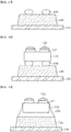
- FIG. 3 to FIG. 12 are sectional views illustrating a method of manufacturing the light emitting device according to the first and second embodiments of the present disclosure.
- FIG. 3 shows a laminate structure in which a support member 150, a light transmitting resin 145 and a photoresist 160 are sequentially stacked in the stated order.
- the support member 150 supports components of the light emitting device in manufacture thereof.
- the support member 150 may be a flat sheet or film.
- the support member 150 may be a flat sheet or film formed of a synthetic resin, glass, or metal.
- the light transmitting resin 145 is stacked on the support member 150.
- the light transmitting resin 145 is formed of a transparent resin allowing transmission of light therethrough.
- the light transmitting resin 145 is formed of a transparent silicone resin.
- the light transmitting resin 145 may be formed by spin coating, printing or rolling the transparent resin.
- the light transmitting resin 145 may be a film formed of a transparent resin.
- the light transmitting resin 145 may be formed of a transparent silicone resin.
- the light transmitting resin 145 may contain phosphors dispersed in the transparent resin.
- the photoresist 160 is formed on the light transmitting resin 145.
- the photoresist 160 is formed of a photosensitive resin.
- the photoresist 160 may be formed on the light transmitting resin 145 by spin coating, printing or rolling, or may be stacked in film form thereon.
- the photoresist 160 is subjected to patterning so as to have an inclined side surface. That is, the photoresist 160 is patterned so as to have a width gradually increasing from an upper portion thereof to a lower portion thereof.
- the photoresist 160 may be subjected to patterning through exposure and development using a patterned mask (not shown).
- the light transmitting resin 145 (see FIG. 4 ) is subjected to patterning.
- the light transmitting resin 145 (see FIG. 4 ) is subjected to patterning through photolithography.
- the light transmitting resin 145 (see FIG. 4 ) is subjected to exposure.
- a portion of the light transmitting resin 145 (see FIG. 4 ) covered by the photoresist 160 is protected from the exposure process and a non-covered portion of the light transmitting resin 145 is subjected to exposure.
- the light transmitting resin 145 (see FIG. 4 ) is subjected to dry or wet etching to remove the exposed portion thereof.
- the photoresist 160 may serve to protect the unexposed portion of the light transmitting resin 145 (see FIG. 4 ) from an etchant for etching.
- the light transmitting resin 145 (see FIG. 4 ) subjected to patterning through photolithography becomes a second light transmitting resin part 140, the width of which is gradually increased from an upper portion thereof to a lower portion thereof, as shown in FIG. 5 .
- the second light transmitting resin part 140 shown in FIG. 5 is the same as the second light transmitting resin part 140 shown in FIG. 1 and FIG. 2 .
- the photoresist 160 (see FIG. 5 ) is removed.
- the photoresist 160 (see FIG. 5 ) may be removed by various methods known in the art.
- a light emitting diode chip 120 is mounted on the second light transmitting resin part 140.
- the light emitting diode chip 120 emits light through upper and side surfaces thereof.
- the light emitting diode chip 120 has bump pads 121 formed on a lower surface thereof.
- the bump pads 121 may be formed of a material reflecting light.
- the bump pads 121 may be formed of a metal. Accordingly, the bump pads 121 serve to prevent light from being emitted through a lower surface of the light emitting diode chip 120.
- a bonding member 122 may be formed on each of the bump pads 121.
- the light emitting diode chip 120 is mounted on the second light transmitting resin part 140 such that the upper surface of the light emitting diode chip 120 adjoins the upper surface of the second light transmitting resin part 140.
- a first light transmitting resin part 130 is formed to cover the side surface of the light emitting diode chip 120.
- a resin member is deposited on the side surface of the light emitting diode chip 120.
- the resin member is a light transmitting resin allowing transmission of light therethrough.
- the resin member may contain phosphors dispersed in the light transmitting resin.
- the resin member has suitable viscosity to flow down on the side surface of the light emitting diode chip 120 while allowing some of the resin member to be kept in a closely contacting state on the side surface of the light emitting diode chip 120.
- the resin member is deposited in an amount so as to cover the side surface of the light emitting diode chip 120 from a portion of the light emitting diode chip 120, at which the side surface of the light emitting diode chip 120 meets the lower surface thereof, to the upper surface of the second light transmitting resin part 140.
- the viscous resin member is deposited on the side surface of the light emitting diode chip 120 to form a first light transmitting resin part 130 that covers the side surface of the light emitting diode chip 120.
- the first light transmitting resin part 130 is formed to cover the side surface of the light emitting diode chip 120 from the portion of the light emitting diode chip 120, at which the side surface of the light emitting diode chip 120 meets the lower surface thereof, to the upper surface of the second light transmitting resin part 140. That is, the first light transmitting resin part 130 covers the entire side surface of the light emitting diode chip 120. Further, an exposed side surface of the first light transmitting resin part 130 is a concavely curved surface.
- a barrier part 110 is formed.
- a barrier part resin 115 is formed on the support member 150.
- the barrier part resin 115 is formed to cover the first light transmitting resin part 130, the second light transmitting resin part 140, and the light emitting diode chip 120.
- the barrier part resin 115 may be formed of a material capable of reflecting light.
- the barrier part resin 115 may be formed of a silicone resin, an epoxy resin, or a thermosetting resin having high heat resistance.
- the barrier part resin 115 may further include a reflective material, such as TiO 2 , SiO 2 , Al 2 O 3 , and the like, in order to improve light reflectivity.
- the barrier part resin 115 may further contain additional substances, such as antioxidants, release materials, inorganic fillers, curing catalysts, light stabilizers, lubricants, and the like.
- the barrier part resin 115 (see FIG. 9 ) is removed.
- the barrier part resin 115 (see FIG. 9 ) is removed to expose the bonding member 122 formed on the light emitting diode chip 120.
- the barrier part resin 115 may be processed by at least one of a mechanical polishing process and a chemical polishing process known in the art.
- the barrier part resin 115 (see FIG. 9 ) may be processed by a grinding process and a fly-cutting process. Through these processes, a barrier part 110 is formed.
- the barrier part 110 is formed to surround the side surface of the first light transmitting resin part 130 and the side surface of the second light transmitting resin part 140.
- An inner wall of the barrier part 110 may be divided into a first inner wall 111 surrounding the side surface of the first light transmitting resin part 130 and a second inner wall 112 surrounding the side surface of the second light transmitting resin part 140. Since the side surface of the first light transmitting resin part 130 is a concave surface, the first inner wall 111 has a convexly curved plane.
- the side surface of the second light transmitting resin part 140 is an inclined surface that has a width gradually increasing with increasing distance from the light emitting diode chip 120
- the second inner wall 112 also has an inclined plane that has a width gradually increasing with increasing distance from the light emitting diode chip 120.
- the support member 150 (see FIG. 10 ) is removed.
- the support member 150 may be removed by applying force to the support member 150 (see FIG. 10 ) to separate the support member 150 from the barrier part 110 and the second light transmitting resin part 140. Additionally, the support member 150 (see FIG. 10 ) may be removed by various methods known in the art.
- a light emitting device 100 By removing the support member 150 (see FIG. 10 ), a light emitting device 100 according to the first embodiment is provided.
- one light emitting device is illustrated by way of example. However, it should be understood that the present disclosure is not limited thereto.
- the barrier part 110 may be formed to cover the entirety of the first light transmitting resin parts 130, the second light transmitting resin parts 140 and the light emitting diode chips 120.
- multiple light emitting devices may be manufactured by dividing adjacent light emitting diode chips 120 from one another through dicing.
- a wavelength conversion part 210 is formed to cover the second light transmitting resin part 140 and the barrier part 110.
- the wavelength conversion part 210 converts the wavelength of light emitted from the second light transmitting resin part 140. That is, the wavelength conversion part 210 converts light emitted from the light emitting diode chip 120 into white light or other colors of light.
- the wavelength conversion part 210 may contain phosphors dispersed in a light transmitting resin.
- the light transmitting resin may be a transparent silicone resin.
- the phosphors may be yellow phosphors, red phosphors, green phosphors, and the like.
- the wavelength conversion part 210 is formed to cover the second light transmitting resin part 140 and the barrier part 110, thereby providing the light emitting device 200 according to the second embodiment.
- FIG. 13 is a sectional view of a light emitting device according to a third embodiment of the present disclosure.
- a light emitting device 100 includes a barrier part 310, a light emitting diode chip 120, a first light transmitting resin part 330, and a second light transmitting resin part 140.
- the barrier part 310 includes a first inner wall 311 adjoining the side surface of the first light transmitting resin part 330 and a second inner wall 312 adjoining the side surface of the second light transmitting resin part 140.
- a lower end of the inner wall of the barrier part 310 adjoins a sidewall between the upper surface of the light emitting diode chip 120 and the lower surface thereof. That is, the lower end of the first inner wall 311 of the barrier part 310 is placed between an upper end of the side surface of the light emitting diode chip 120 and a lower end thereof.
- the lower end of the first inner wall 311 adjoins a side surface of a component placed under the growth substrate of the light emitting diode chip 120.
- the upper end of the first inner wall 311 is coplanar with the upper surface of the light emitting diode chip 120.
- the first light transmitting resin part 330 is formed to surround the side surface of the growth substrate of the light emitting diode chip 120 while partially surrounding the side surface of the semiconductor laminate or without surrounding the side surface of the semiconductor laminate. With this structure, a portion of the side surface of the light emitting diode chip 120 closely contacts the barrier part 310.
- the second inner wall 312 of the barrier part 310 has an inclined plane in cross-sectional view, like the second inner wall 112 (see FIG. 1 ) of the barrier part 110 (see FIG. 1 ) in the light emitting device according to the above embodiment.
- the light emitting device 100 has a larger contact area between the barrier part 310 and the light emitting diode chip 120 than that of the light emitting device according to the above embodiment. With this structure, the light emitting diode chip 120 can be more effectively secured inside the barrier part 310.
- FIG. 14 and FIG. 15 are sectional views illustrating a method of manufacturing the light emitting device according to the third embodiment of the present disclosure.
- a first light transmitting resin part 330 is formed on a side surface of a light emitting diode chip 120.
- a second light transmitting resin part 140 subjected to patterning to have an inclined side surface is formed on a support member 150.
- the light emitting diode chip 120 is disposed on the second light transmitting resin part 140 such that an upper surface of the light emitting diode chip 120 adjoins an upper surface of the second light transmitting resin part 140.
- a resin member having viscosity is deposited on the side surface of the light emitting diode chip 120.
- the resin member flows down toward an upper portion of the second light transmitting resin part 140 along the side surface of the light emitting diode chip 120.
- the resin member deposited on the side surface of the light emitting diode chip 120 may also cover a portion of the side surface of the light emitting diode chip 120. That is, in this embodiment, a smaller amount of the resin member is used to form the first light transmitting resin part than the amount of the resin member used to form the first light transmitting resin part 130 (see FIG. 8 ) in the first or second embodiment.
- the amount of the resin member is determined to surround the side surface of the growth substrate of the light emitting diode chip 120 while partially surrounding the side surface of the semiconductor laminate grown on the growth substrate or without surrounding the side surface of the semiconductor laminate.
- the first light transmitting resin part 330 is formed by depositing the resin member so as to surround a portion of the side surface of the light emitting diode chip 120.
- a barrier part 310 is formed on the support member 150 to surround the first light transmitting resin part 330, the second light transmitting resin part 140 and the light emitting diode chip 120.
- FIG. 9 For details of a method for forming the barrier part 310, refer to FIG. 9 and FIG. 10 .
- the barrier part 310 is formed to surround the side surface of each of the first light transmitting resin part 330 and the second light transmitting resin part 140. In addition, the barrier part 310 is formed to surround a portion of the side surface of the light emitting diode chip 120 and the lower surface thereof. Here, referring to FIG. 15 , at least part of a bonding member 122 formed on the light emitting diode chip 120 is exposed to an upper surface of the barrier part 310.
- the support member 150 is removed from the components shown in FIG. 15 , thereby providing the light emitting device 300 according to the third embodiment shown in FIG. 13 .
- a wavelength conversion part (not shown) may be further formed to cover the barrier part 310 and the second light transmitting resin part 140 of the light emitting device 300 (see FIG. 13 ).
- FIG. 16 is a sectional view of a light emitting device according to a fourth embodiment of the present disclosure.
- a light emitting device 400 includes a barrier part 410, a light emitting diode chip 120, a first light transmitting resin part 430, and a second light transmitting resin part 140.
- the barrier part 410 includes a first inner wall 411 adjoining a side surface of a first light transmitting resin part 430 and a second inner wall 412 adjoining a side surface of the second light transmitting resin part 140.
- the first inner wall 411 of the barrier part 410 has a convexly curved plane in cross-section view, as shown in the drawings.
- the second inner wall 412 of the barrier part 410 has an inclined plane in cross-section view, like the second inner wall 112 (see FIG. 1 ) of the barrier part 110 (see FIG. 1 ) according to the above embodiment.
- a lower end of a sidewall of the light emitting diode chip 120 adjoins a lower end of a sidewall of the barrier part 410. That is, the lower end of the first inner wall 411 of the barrier part 410 adjoins the lower end of the sidewall of the light emitting diode chip 120.
- the first light transmitting resin part 430 and the second light transmitting resin part 140 may be formed of a light transmitting resin such as a transparent silicone resin. Alternatively, at least one of the first light transmitting resin part 430 and the second light transmitting resin part 140 may contain phosphors dispersed in the light transmitting resin.
- the first light transmitting resin part 430 is formed to cover a side surface and an upper surface of the light emitting diode chip 120.
- the second light transmitting resin part 140 is formed to cover the upper surface of the first light transmitting resin part 430.
- An entire lower surface of the second light transmitting resin part 140 closely contacts the first light transmitting resin part 430 including the same material as the second light transmitting resin part 140. As a result, high adhesion is secured between the first light transmitting resin part 430 and the second light transmitting resin part 140, thereby improving durability of the light emitting device 400.
- FIG. 17 to FIG. 20 are sectional views illustrating a method of manufacturing the light emitting device according to the fourth embodiment of the present disclosure.
- a resin member 435 is disposed on the second light transmitting resin part 140.
- the resin member 435 is formed of a light transmitting resin.
- the resin member 435 may contain phosphors dispersed in the light transmitting resin.
- the light transmitting resin may be a transparent silicone resin.
- the resin member 435 may have suitable viscosity to be deformed depending upon the magnitude of force applied thereto while preventing the resin member 435 from flowing along the surface of the second light transmitting resin part 140. Accordingly, the resin member 435 may be kept in a deposited state on the upper surface of the second light transmitting resin part 140.
- the second light transmitting resin part 140 is formed on the support member 150. Further, the second light transmitting resin part 140 is formed to have a width gradually narrowing with increasing distance from an upper surface of the support member 150. For a method of forming the second light transmitting resin part 140, refer to FIG. 3 to FIG. 6 .
- a light emitting diode chip 120 is mounted on the resin member 435.
- the light emitting diode chip 120 With an upper surface of the light emitting diode chip 120 facing the upper surface of the second light transmitting resin part 140, the light emitting diode chip 120 is mounted on the resin member 435.
- a first light transmitting resin part 430 is formed to surround the upper and side surfaces of the light emitting diode chip 120.
- the resin member 435 (see FIG. 18 ) is compressed by the light emitting diode chip 120. Then, a portion of the resin member 435 (see FIG. 18 ) flows along the surface of the light emitting diode chip 120 to surround the entirety of the side surface of the light emitting diode chip 120 by the applied force. As such, some of the resin member 435 (see FIG. 18 ) covers the upper surface of the light emitting diode chip 120 and the other resin member 435 covers the entire side surface of the light emitting diode chip 120 to form the first light transmitting resin part 430.
- a barrier part 410 is formed to surround the first light transmitting resin part 430, the second light transmitting resin part 140 and the light emitting diode chip 120 on the support member 150.
- a method of forming the barrier part 410 refer to FIG. 9 and FIG. 10 .
- the barrier part 410 includes a cavity in which the first light transmitting resin part 430, the second light transmitting resin part 140 and the light emitting diode chip 120 are disposed.
- An inner wall of the barrier part 410 defining the cavity is formed to surround side surfaces of the first light transmitting resin part 430 and the second light transmitting resin part 140. Accordingly, the first inner wall 411 surrounding the side surface of the first light transmitting resin part 430 has a convexly curved plane in cross-section view and the second inner wall 412 surrounding the side surface of the second light transmitting resin part 140 has an inclined plane in cross-sectional view. An upper end of the first inner wall 411 is placed higher than the upper surface of the light emitting diode chip 120.
- the barrier part 410 is formed to surround a portion of the side surface of the light emitting diode chip 120 and a lower surface thereof.
- the support member 150 is removed from the components shown in FIG. 20 , thereby providing the light emitting device 400 according to the fourth embodiment shown in FIG. 16 .
- a wavelength conversion part (not shown) may be further formed to cover the barrier part 410 and the second light transmitting resin part 140 of the light emitting device 400 (see FIG. 16 ).
- FIG. 21 is a sectional view of a light emitting device according to a fifth embodiment of the present disclosure.
- a light emitting device 500 includes a barrier part 510, a light emitting diode chip 120, a first light transmitting resin part 530, and a second light transmitting resin part 140.
- An inner wall of the barrier part 510 may be divided into a first inner wall 511 adjoining a side surface of the first light transmitting resin part 530 and a second inner wall 512 adjoining a side surface of the second light transmitting resin part 140.
- the first light transmitting resin part 530 is formed to cover a portion of a side surface of the light emitting diode chip 120 and an upper surface thereof. Further, the second light transmitting resin part 140 is formed to cover an upper surface of the first light transmitting resin part 530.
- a lower end of the first light transmitting resin part 530 adjoins the side surface of the light emitting diode chip 120. More specifically, the first light transmitting resin part 530 surrounds a side surface of a growth substrate of the light emitting diode chip 120 while partially surrounding the side surface of the semiconductor laminate or without surrounding the side surface of the semiconductor laminate. Accordingly, a portion of the side surface of the light emitting diode chip 120 closely contacts the barrier part 510.
- a bonding area between the barrier part 510 and the light emitting diode chip 120 is increased above the bonding area therebetween according to the fourth embodiment, whereby the light emitting diode chip 120 can be more effectively secured inside the barrier part 510.
- the entire lower surface of the second light transmitting resin part 140 closely contacts the first light transmitting resin part 530, thereby improving adhesion between the first light transmitting resin part 530 and the second light transmitting resin part 140.
- the light emitting device 500 according to this embodiment has improved durability through improvement in securing force and adhesive strength between the components thereof.
- FIG. 22 to FIG. 24 are sectional views illustrating a method of manufacturing the light emitting device according to the fifth embodiment.
- a light emitting diode chip 120 is mounted on a resin member 535 disposed on a second light transmitting resin part 140.
- the light emitting diode chip 120 is mounted on the resin member 535 such that the upper surface of the light emitting diode chip 120 faces the upper surface of the second light transmitting resin part 140.
- the resin member 535 is deposited in a smaller amount than the resin member 435 (see FIG. 17 ) on the second light transmitting resin part 140 in the fourth embodiment.
- the amount of the resin member 435 is determined to surround the entire side surface of the light emitting diode chip 120, the amount of the resin member 535 according to this embodiment is smaller than the amount of the resin member 435 (see FIG. 17 ) according to the fourth embodiment.
- a first light transmitting resin part 530 is formed to surround the upper surface of the light emitting diode chip 120 and a portion of a side surface thereof.
- the resin member 535 (see FIG. 22 ) is compressed by the light emitting diode chip 120 placed thereon. Some of the resin member 535 (see FIG. 22 ) flows along the surface of the light emitting diode chip 120 to surround a portion of the side surface of the light emitting diode chip 120 by the applied force. Here, the degree of surrounding the side surface of the light emitting diode chip 120 is changed depending upon the amount of the resin member 535 (see FIG. 22 ).
- some of the resin member 535 covers the upper surface of the light emitting diode chip 120 and the other resin member 535 covers a portion of the side surface of the light emitting diode chip 120 to form the first light transmitting resin part 530.
- a barrier part 510 is formed to surround the first light transmitting resin part 530, the second light transmitting resin part 140 and the light emitting diode chip 120 on a support member 150.
- a method of forming the barrier part 510 refer to FIG. 9 and FIG. 10 .
- the barrier part 510 includes a cavity in which the light emitting diode chip 120, the first light transmitting resin part 530 and the second light transmitting resin part 140 are disposed.
- a first inner wall 511 surrounding the side surface of the first light transmitting resin part 530 has a convexly curved plane and the second inner wall 512 surrounding the side surface of the second light transmitting resin part 140 has an inclined plane.
- An upper end of the first inner wall 511 is placed higher than the upper surface of the light emitting diode chip 120. Further, a lower end of the first inner wall 511 adjoins the side surface of the light emitting diode chip 120. Accordingly, a portion of the side surface of the light emitting diode chip 120 closely contacts the barrier part 510.
- a wavelength conversion part (not shown) may be further formed to cover the barrier part 510 and the second light transmitting resin part 140 of the light emitting device 500.
Landscapes
- Led Device Packages (AREA)
Abstract
Description
- Embodiments of the present disclosure relate to a light emitting device.
- Generally, a light emitting device (LED) including a light emitting diode chip is used as a light source in various fields, such as a light source for backlights and the like.
- The light emitting device emits light having various wavelengths through recombination of electrons and holes in a junction between a p-type semiconductor and an n-type semiconductor upon application of electric current thereto. Due to various advantages of light emitting device, such as longer lifespan, lower power consumption, and better operation characteristics than filaments used in a typical light emitting apparatus, there is increasing demand for the light emitting devices.
- In a typical light emitting device, a light emitting diode chip is disposed in a cavity of a barrier. Further, a side surface of the light emitting diode chip closely contacts an inner wall defining the cavity of the barrier. Here, light emitted through the side surface of the light emitting diode chip can be reabsorbed into the light emitting diode chip through light loss or reflection on the inner wall of the barrier closely contacting the light emitting diode chip.
- Embodiments of the present disclosure provide a light emitting device having improved luminous efficacy.
- Embodiments of the present disclosure provide a light emitting device having improved durability through improvement in adhesion between components thereof.
- In accordance with embodiments of the present disclosure, there is provided a light emitting device including: a light emitting diode chip, a first light transmitting resin part, a second light transmitting resin part, and a barrier part. The second light transmitting resin part covers an upper portion of the first light transmitting resin part and an upper portion of the light emitting diode chip. The barrier part surrounds side surfaces of the light emitting diode chip, the first light transmitting resin part and the second light transmitting resin part and a lower surface of the light emitting diode chip. Here, each of the first light transmitting resin part and the second light transmitting resin part has a width gradually increasing from a lower portion thereof to the upper portion thereof. Further, the inner wall of the barrier part adjoins the side surface of the light emitting diode chip or a lower end of the side surface thereof. The inner wall of the barrier part is divided into a first inner wall having a convexly curved plane and a second inner wall having an inclined plane in cross-sectional view.
- According to embodiments of the present disclosure, the light emitting device and the method of manufacturing the same ensure improvement in luminous efficacy by preventing loss of light emitted through a side surface of a light emitting diode chip.
- According to embodiments of the present disclosure, the light emitting device and the method of manufacturing the same can enhance durability through improvement in adhesion between components therebetween.
-
-
FIG. 1 is a sectional view of a light emitting device according to a first embodiment of the present disclosure. -
FIG. 2 is a sectional view of a method of manufacturing a light emitting device according to a second embodiment of the present disclosure. -
FIG. 3 to FIG. 12 are sectional views illustrating a method of manufacturing the light emitting device according to the first and second embodiments of the present disclosure. -
FIG. 13 is a sectional view of a light emitting device according to a third embodiment of the present disclosure. -
FIG. 14 and FIG. 15 are sectional views illustrating a method of manufacturing the light emitting device according to the third embodiment of the present disclosure. -
FIG. 16 is a sectional view of a light emitting device according to a fourth embodiment of the present disclosure. -
FIG. 17 to FIG. 20 are sectional views illustrating a method of manufacturing the light emitting device according to the fourth embodiment of the present disclosure. -
FIG. 21 is a sectional view of a light emitting device according to a fifth embodiment of the present disclosure. -
FIG. 22 to FIG. 24 are sectional views illustrating a method of manufacturing the light emitting device according to the fifth embodiment of the present disclosure. - Hereinafter, embodiments of the present disclosure will be described in detail with reference to the accompanying drawings. The following embodiments are provided by way of example so as to fully convey the spirit of the present disclosure to those skilled in the art to which the present disclosure pertains. Accordingly, the present disclosure is not limited to the embodiments disclosed herein and can also be implemented in different forms. In the drawings, widths, lengths, thicknesses, and the like of elements can be exaggerated for clarity and descriptive purposes. Throughout the specification, like reference numerals denote like elements having the same or similar functions.
- A light emitting device according to embodiments of the present disclosure includes a light emitting diode chip, a first light transmitting resin part, a second light transmitting resin part, and a barrier part.
- The light emitting diode chip emits light. The first light transmitting resin part is formed to surround at least part of a side surface of the light emitting diode chip. The second light transmitting resin part is formed to cover an upper portion of the first light transmitting resin part and an upper portion of the light emitting diode chip. The barrier part is formed to surround side surfaces of the light emitting diode chip, the first light transmitting resin part and the second light transmitting resin part and a lower surface of the light emitting diode chip. Here, each of the first light transmitting resin part and the second light transmitting resin part has a width gradually increasing from a lower portion thereof to the upper portion thereof. Further, the inner wall of the barrier part adjoins the side surface of the light emitting diode chip or a lower end of the side surface thereof. The inner wall of the barrier part is divided into a first inner wall having a convexly curved plane and a second inner wall having an inclined plane in cross-sectional view.
- The first inner wall of the barrier part surrounds the side surface of the first light transmitting resin part and the second inner wall of the barrier part surrounds the side surface of the second light transmitting resin part.
- The side surface of the first light transmitting resin part may closely contact the first inner wall of the barrier part and includes a concavely curved plane.
- The side surface of the second light transmitting resin part may closely contact the second inner wall of the barrier part and includes an inclined plane.
- A lower end of the first inner wall of the barrier part may adjoin the lower end of the side surface of the light emitting diode chip.
- A lower end of the first inner wall of the barrier part is placed at a height spaced apart from the lower end of the light emitting diode chip while adjoining the side surface of the light emitting diode chip.
- An upper end of the first inner wall of the barrier part is coplanar with an upper surface of the light emitting diode chip.
- A lower surface of the second light transmitting resin part adjoins an upper surface of the first light transmitting resin part and the upper surface of the light emitting diode chip.
- An upper end of the first inner wall of the barrier part is placed higher than the upper surface of the light emitting diode chip.
- The first light transmitting resin part surrounds at least part of the side surface of the light emitting diode chip and the upper surface thereof. Here, an entire lower surface of the second light transmitting resin part may adjoin the upper surface of the first light transmitting resin part.
- The first light transmitting resin part and the second light transmitting resin part are transparent resins allowing transmission of light therethrough.
- For example, the transparent resins are transparent silicone resins.
- At least one of the first light transmitting resin part and the second light transmitting resin part may further include a phosphor.
- The light emitting device may further include a wavelength conversion part covering an upper surface of the second light transmitting resin part and an upper surface of the barrier part.
- For example, the wavelength conversion part may be phosphor-in-glass (PIG).
- The inner wall of the barrier part may reflect light emitted from the light emitting diode chip.
- The light emitting diode chip is formed with a bump pad formed on the lower surface thereof and connected to an electrode thereof.
- At least part of the bump pad of the light emitting diode chip is embedded in the barrier part.
- The light emitting device may further include a bonding member formed on a lower portion of the bump pad.
- At least part of the bonding member is exposed from a lower surface of the barrier part.
- Hereinafter, embodiments of the present disclosure will be described in detail. Unless stated otherwise, the following description will be given with reference to the accompanying drawings.
- For example, description that the first inner wall of the barrier part is composed of a convexly curved plane and the second inner wall is composed of an inclined plane is given with reference to cross-sectional views of the light emitting device shown in the drawings. Accordingly, it should be understood that the following description with regard to components is given with reference to the accompany drawings.
- For convenience of description and understanding, the cavity of the barrier part according to the present disclosure is defined as a space inside the barrier part in which the light emitting diode chip, the first light transmitting resin part, and the second light transmitting resin part are disposed.
-
FIG. 1 is a sectional view of a light emitting device according to a first embodiment of the present disclosure. - Referring to
FIG. 1 , alight emitting device 100 according to the first embodiment includes abarrier part 110, a light emittingdiode chip 120, a first light transmittingresin part 130, and a second light transmittingresin part 140. - The
barrier part 110 includes a cavity. Referring toFIG. 1 , the cavity refers to a space of thebarrier part 110 in which the light emittingdiode chip 120, the first light transmittingresin part 130 and the second light transmittingresin part 140 are disposed. The cavity is defined inside thebarrier part 110 and has a structure that opens a portion of an upper surface of thebarrier part 110. The cavity has a width gradually narrowing from an upper portion of thebarrier part 110 to a lower portion thereof. As shown in the drawings, the light emittingdiode chip 120 is mounted inside the cavity formed in thebarrier part 110. - An inner wall of the
barrier part 110 defining the cavity is divided into a firstinner wall 111 and a secondinner wall 112. As shown in the drawings, the firstinner wall 111 has a convexly curved plane and the secondinner wall 112 has an inclined plane. The firstinner wall 111 is disposed between an inner bottom surface of thebarrier part 110 defining the cavity and the secondinner wall 112. In addition, the secondinner wall 112 is disposed between the firstinner wall 111 and the upper surface of thebarrier part 110. - The
barrier part 110 reflects light emitted from the light emittingdiode chip 120. For example, thebarrier part 110 is formed of a material capable of reflecting light. - The light emitting
diode chip 120 includes a semiconductor laminate grown on a growth substrate for growth of semiconductor layers. For example, the semiconductor laminate may be formed of aluminum gallium arsenide, gallium arsenide phosphorus, indium gallium nitride, gallium phosphide, zinc selenide, aluminum indium gallium phosphorus, diamond, zinc oxide, and the like. The light emittingdiode chip 120 emits light in different wavelength bands depending upon the material of the semiconductor laminate. - The light emitting
diode chip 120 is provided at a lower side thereof with electrodes (not shown) and bumppads 121 electrically connected to the electrodes. Thebump pads 121 protrude downwards from a lower surface of the light emittingdiode chip 120. Thebump pads 121 connect the light emittingdiode chip 120 to an external circuit board (not shown). With this structure, the light emittingdiode chip 120 is mounted on the external circuit board through flip-chip bonding. - The
bump pads 121 of the light emittingdiode chip 120 are embedded in thebarrier part 110 under the cavity. As a result, the lower surface of the light emittingdiode chip 120 adjoins a bottom surface of the cavity. - Further, the
bonding member 122 is formed on thebump pad 121 of the light emittingdiode chip 120. Thebonding member 122 serves to bond thebump pad 121 to the external circuit board and is formed of an electrically conductive material. Accordingly, thebonding member 122 is exposed from a lower surface of thebarrier part 110. For example, thebonding member 122 may be a solder. - In this embodiment, the
bump pads 121 and thebonding members 122 are formed on the lower surface of the light emittingdiode chip 120. However, it should be understood that the light emitting device according to the present disclosure is not limited to the structure wherein the light emitting device includes both thebump pad 121 and thebonding member 122. Alternatively, thelight emitting device 100 may include at least one of thebump pad 121 and thebonding member 122. For thelight emitting device 100 not including thebonding members 122, thebump pads 121 connected to the electrodes of the light emittingdiode chip 120 may be exposed from the lower surface of thebarrier part 110. Further, for thelight emitting device 100 not including thebump pads 121, thebonding members 122 at least partially exposed from the lower surface of thebarrier part 110 may be directly connected to the electrodes of the light emittingdiode chip 120. - A lower end of the sidewall of the light emitting
diode chip 120 adjoins a lower end of the sidewall of thebarrier part 110. That is, the lower end of the firstinner wall 111, which is a convexly curved plane of thebarrier part 110, adjoins the lower end of the sidewall of the light emittingdiode chip 120. Here, the lower end of the light emittingdiode chip 120 refers to a portion of the light emittingdiode chip 120 at which the lower surface of the light emittingdiode chip 120 adjoins a side surface thereof. Further, an upper end of the firstinner wall 111 is coplanar with an upper surface of the light emittingdiode chip 120. - The first light transmitting
resin part 130 is formed to surround the side surface of the light emittingdiode chip 120 disposed inside the cavity of thebarrier part 110. That is, the first light transmittingresin part 130 is surrounded by the firstinner wall 111. Accordingly, the side surface of the first light transmittingresin part 130 is convexly curved corresponding to the curved plane of the firstinner wall 111. The first light transmittingresin part 130 is formed of a transparent resin allowing transmission of light therethrough. For example, the first light transmittingresin part 130 may be formed of a transparent silicone resin. - The second light transmitting
resin part 140 is formed to cover the upper surfaces of the light emittingdiode chip 120 and the first light transmittingresin part 130 inside the cavity of thebarrier part 110. That is, the second light transmittingresin part 140 is surrounded by the second inner wall. Accordingly, the side surface of the second light transmittingresin part 140 has a planar structure corresponding to the second inner wall. The second light transmittingresin part 140 is formed of a transparent resin allowing transmission of light therethrough. For example, the second light transmittingresin part 140 is formed of a transparent silicone resin. - The first light transmitting
resin part 130 and the second light transmittingresin part 140 may be formed of a transparent resin alone. In one embodiment, at least one of the first light transmittingresin part 130 and the second light transmittingresin part 140 may contain phosphors dispersed in the transparent resin. In this embodiment, light emitted from the light emittingdiode chip 120 is subjected to wavelength conversion by the phosphors and then discharged from thelight emitting device 100. When both the first light transmittingresin part 130 and the second light transmittingresin part 140 include the phosphors, the phosphor contained in the first light transmittingresin part 130 may be the same as the phosphor contained in the second light transmittingresin part 140. Alternatively, the phosphor of the first light transmittingresin part 130 and the phosphor of the second light transmittingresin part 140 may be formed of different materials to convert light having a certain wavelength into light in different wavelength bands. - The light emitting
diode chip 120 emits light not only through the upper surface thereof but also through the side surface thereof. However, in a typical light emitting device, the inner wall of the barrier part closely contacts the entire side surface of the light emitting diode chip. As a result, the typical light emitting device has a problem of light loss by the barrier part when light is emitted from the side surface of the light emitting diode chip. - In the
light emitting device 100 according to this embodiment, a space is defined between the light emittingdiode chip 120 and the inner wall of thebarrier part 110. Accordingly, thelight emitting device 100 can prevent light emitted through the side surface of the light emittingdiode chip 120 from being lost by the inner wall of thebarrier part 110. Further, in thelight emitting device 100 according to this embodiment, light emitted through the side surface of the light emittingdiode chip 120 is reflected by the inner wall of thebarrier part 110 and discharged through the upper surface of the second light transmittingresin part 140. Accordingly, thelight emitting device 100 allows light emitted through the side surface of the light emittingdiode chip 120 to be discharged outside by preventing loss of the light emitted therethrough, thereby improving luminous efficacy. - Further, the
light emitting device 100 according to this embodiment includes the firstinner wall 111 having a convexly curved plane. The firstinner wall 111 serves to reflect light upwardly of the second light transmittingresin part 140. Thus, thelight emitting device 100 according to this embodiment can prevent light emitted from the light emittingdiode chip 120 from being reabsorbed into the light emittingdiode chip 120. - Further, as shown in
FIG. 1 , in thelight emitting device 100 according to this embodiment, the inner wall of thebarrier part 110 is formed to have a sharp inclination. Accordingly, thelight emitting device 100 may be applied to products requiring light directionality. For example, thelight emitting device 100 may be applied to vehicular head lamps or an edge of a display panel to improve light directionality. - The following description with respect to light emitting devices according to other embodiments and methods of manufacturing the same will focus on different features from the light emitting device according to the above embodiment. For details of omitted components in the following description, refer to the description of the light emitting device according to this embodiment.
-
FIG. 2 is a sectional view of a method of manufacturing a light emitting device according to a second embodiment of the present disclosure. - Referring to
FIG. 2 , alight emitting device 200 according to the second embodiment includes abarrier part 110, a light emittingdiode chip 120, a first light transmittingresin part 130, a second light transmittingresin part 140, and awavelength conversion part 210. - The
wavelength conversion part 210 is formed to cover upper surfaces of the second light transmittingresin part 140 and thebarrier part 110. Thewavelength conversion part 210 converts the wavelength of light emitted from the light emittingdiode chip 120. - The
wavelength conversion part 210 may contain phosphors dispersed in a light transmitting resin and converting the wavelength of light. For example, the light transmitting resin may be a transparent silicone resin. The phosphors may be yellow phosphors, red phosphors, or green phosphors, or may be selected from any phosphors capable of converting the wavelength of light. Alternatively, thewavelength conversion part 210 may be phosphor-in-glass (PIG) in which the phosphor is mixed in glass. - Light emitted from the light emitting
diode chip 120 is converted by thewavelength conversion part 210, whereby thelight emitting device 200 can emit white light or other colors of light. - Further, the
wavelength conversion part 210 covers the upper surfaces of the second light transmittingresin part 140 and thebarrier part 110, thereby preventing foreign matter, such as moisture, dust and the like, from entering thelight emitting device 200. - According to this embodiment, the first light transmitting
resin part 130 and the second light transmittingresin part 140 may include the phosphors or may be free from the phosphors. -
FIG. 3 to FIG. 12 are sectional views illustrating a method of manufacturing the light emitting device according to the first and second embodiments of the present disclosure. -
FIG. 3 shows a laminate structure in which asupport member 150, alight transmitting resin 145 and aphotoresist 160 are sequentially stacked in the stated order. Thesupport member 150 supports components of the light emitting device in manufacture thereof. Thesupport member 150 may be a flat sheet or film. For example, thesupport member 150 may be a flat sheet or film formed of a synthetic resin, glass, or metal. - The
light transmitting resin 145 is stacked on thesupport member 150. Thelight transmitting resin 145 is formed of a transparent resin allowing transmission of light therethrough. For example, thelight transmitting resin 145 is formed of a transparent silicone resin. Thelight transmitting resin 145 may be formed by spin coating, printing or rolling the transparent resin. Thelight transmitting resin 145 may be a film formed of a transparent resin. For example, thelight transmitting resin 145 may be formed of a transparent silicone resin. Further, thelight transmitting resin 145 may contain phosphors dispersed in the transparent resin. - The
photoresist 160 is formed on thelight transmitting resin 145. Thephotoresist 160 is formed of a photosensitive resin. Thephotoresist 160 may be formed on thelight transmitting resin 145 by spin coating, printing or rolling, or may be stacked in film form thereon. - Referring to
FIG. 4 , thephotoresist 160 is subjected to patterning so as to have an inclined side surface. That is, thephotoresist 160 is patterned so as to have a width gradually increasing from an upper portion thereof to a lower portion thereof. - For example, the
photoresist 160 may be subjected to patterning through exposure and development using a patterned mask (not shown). - Referring to
FIG. 5 , the light transmitting resin 145 (seeFIG. 4 ) is subjected to patterning. - The light transmitting resin 145 (see
FIG. 4 ) is subjected to patterning through photolithography. - The light transmitting resin 145 (see
FIG. 4 ) is subjected to exposure. Here, a portion of the light transmitting resin 145 (seeFIG. 4 ) covered by thephotoresist 160 is protected from the exposure process and a non-covered portion of thelight transmitting resin 145 is subjected to exposure. Thereafter, the light transmitting resin 145 (seeFIG. 4 ) is subjected to dry or wet etching to remove the exposed portion thereof. Here, thephotoresist 160 may serve to protect the unexposed portion of the light transmitting resin 145 (seeFIG. 4 ) from an etchant for etching. - As such, the light transmitting resin 145 (see
FIG. 4 ) subjected to patterning through photolithography becomes a second light transmittingresin part 140, the width of which is gradually increased from an upper portion thereof to a lower portion thereof, as shown inFIG. 5 . The second light transmittingresin part 140 shown inFIG. 5 is the same as the second light transmittingresin part 140 shown inFIG. 1 and FIG. 2 . - Referring to
FIG. 6 , the photoresist 160 (seeFIG. 5 ) is removed. The photoresist 160 (seeFIG. 5 ) may be removed by various methods known in the art. - Referring to
FIG. 7 , a light emittingdiode chip 120 is mounted on the second light transmittingresin part 140. The light emittingdiode chip 120 emits light through upper and side surfaces thereof. Further, the light emittingdiode chip 120 hasbump pads 121 formed on a lower surface thereof. Thebump pads 121 may be formed of a material reflecting light. For example, thebump pads 121 may be formed of a metal. Accordingly, thebump pads 121 serve to prevent light from being emitted through a lower surface of the light emittingdiode chip 120. Further, abonding member 122 may be formed on each of thebump pads 121. - The light emitting
diode chip 120 is mounted on the second light transmittingresin part 140 such that the upper surface of the light emittingdiode chip 120 adjoins the upper surface of the second light transmittingresin part 140. - Referring to
FIG. 8 , a first light transmittingresin part 130 is formed to cover the side surface of the light emittingdiode chip 120. A resin member is deposited on the side surface of the light emittingdiode chip 120. The resin member is a light transmitting resin allowing transmission of light therethrough. Alternatively, the resin member may contain phosphors dispersed in the light transmitting resin. The resin member has suitable viscosity to flow down on the side surface of the light emittingdiode chip 120 while allowing some of the resin member to be kept in a closely contacting state on the side surface of the light emittingdiode chip 120. The resin member is deposited in an amount so as to cover the side surface of the light emittingdiode chip 120 from a portion of the light emittingdiode chip 120, at which the side surface of the light emittingdiode chip 120 meets the lower surface thereof, to the upper surface of the second light transmittingresin part 140. - As such, the viscous resin member is deposited on the side surface of the light emitting
diode chip 120 to form a first light transmittingresin part 130 that covers the side surface of the light emittingdiode chip 120. Further, the first light transmittingresin part 130 is formed to cover the side surface of the light emittingdiode chip 120 from the portion of the light emittingdiode chip 120, at which the side surface of the light emittingdiode chip 120 meets the lower surface thereof, to the upper surface of the second light transmittingresin part 140. That is, the first light transmittingresin part 130 covers the entire side surface of the light emittingdiode chip 120. Further, an exposed side surface of the first light transmittingresin part 130 is a concavely curved surface. - Referring to
FIG. 9 and FIG. 10 , abarrier part 110 is formed. - Referring to
FIG. 9 , abarrier part resin 115 is formed on thesupport member 150. Thebarrier part resin 115 is formed to cover the first light transmittingresin part 130, the second light transmittingresin part 140, and the light emittingdiode chip 120. - The
barrier part resin 115 may be formed of a material capable of reflecting light. For example, thebarrier part resin 115 may be formed of a silicone resin, an epoxy resin, or a thermosetting resin having high heat resistance. Further, thebarrier part resin 115 may further include a reflective material, such as TiO2, SiO2, Al2O3, and the like, in order to improve light reflectivity. Thebarrier part resin 115 may further contain additional substances, such as antioxidants, release materials, inorganic fillers, curing catalysts, light stabilizers, lubricants, and the like. - Referring to
FIG. 10 , a portion of the barrier part resin 115 (seeFIG. 9 ) is removed. The barrier part resin 115 (seeFIG. 9 ) is removed to expose thebonding member 122 formed on the light emittingdiode chip 120. The barrier part resin 115 (seeFIG. 9 ) may be processed by at least one of a mechanical polishing process and a chemical polishing process known in the art. For example, the barrier part resin 115 (seeFIG. 9 ) may be processed by a grinding process and a fly-cutting process. Through these processes, abarrier part 110 is formed. - The
barrier part 110 is formed to surround the side surface of the first light transmittingresin part 130 and the side surface of the second light transmittingresin part 140. An inner wall of thebarrier part 110 may be divided into a firstinner wall 111 surrounding the side surface of the first light transmittingresin part 130 and a secondinner wall 112 surrounding the side surface of the second light transmittingresin part 140. Since the side surface of the first light transmittingresin part 130 is a concave surface, the firstinner wall 111 has a convexly curved plane. Further, since the side surface of the second light transmittingresin part 140 is an inclined surface that has a width gradually increasing with increasing distance from the light emittingdiode chip 120, the secondinner wall 112 also has an inclined plane that has a width gradually increasing with increasing distance from the light emittingdiode chip 120. - Referring to
FIG. 11 , the support member 150 (seeFIG. 10 ) is removed. The support member 150 (seeFIG. 10 ) may be removed by applying force to the support member 150 (seeFIG. 10 ) to separate thesupport member 150 from thebarrier part 110 and the second light transmittingresin part 140. Additionally, the support member 150 (seeFIG. 10 ) may be removed by various methods known in the art. - By removing the support member 150 (see
FIG. 10 ), alight emitting device 100 according to the first embodiment is provided. - In the method of forming the light emitting device according to the present disclosure, one light emitting device is illustrated by way of example. However, it should be understood that the present disclosure is not limited thereto. For example, after multiple first light transmitting
resin parts 130, multiple second light transmittingresin parts 140 and multiple light emittingdiode chips 120 are formed and disposed on a single support member 150 (seeFIG. 3 ), thebarrier part 110 may be formed to cover the entirety of the first light transmittingresin parts 130, the second light transmittingresin parts 140 and the light emitting diode chips 120. Then, multiple light emitting devices may be manufactured by dividing adjacent light emittingdiode chips 120 from one another through dicing. - Referring to
FIG. 12 , awavelength conversion part 210 is formed to cover the second light transmittingresin part 140 and thebarrier part 110. Thewavelength conversion part 210 converts the wavelength of light emitted from the second light transmittingresin part 140. That is, thewavelength conversion part 210 converts light emitted from the light emittingdiode chip 120 into white light or other colors of light. - The
wavelength conversion part 210 may contain phosphors dispersed in a light transmitting resin. For example, the light transmitting resin may be a transparent silicone resin. Further, the phosphors may be yellow phosphors, red phosphors, green phosphors, and the like. - The
wavelength conversion part 210 is formed to cover the second light transmittingresin part 140 and thebarrier part 110, thereby providing thelight emitting device 200 according to the second embodiment. -
FIG. 13 is a sectional view of a light emitting device according to a third embodiment of the present disclosure. - Referring to
FIG. 13 , alight emitting device 100 according to the third embodiment includes abarrier part 310, a light emittingdiode chip 120, a first light transmittingresin part 330, and a second light transmittingresin part 140. - The
barrier part 310 includes a firstinner wall 311 adjoining the side surface of the first light transmittingresin part 330 and a secondinner wall 312 adjoining the side surface of the second light transmittingresin part 140. - According to this embodiment, a lower end of the inner wall of the
barrier part 310 adjoins a sidewall between the upper surface of the light emittingdiode chip 120 and the lower surface thereof. That is, the lower end of the firstinner wall 311 of thebarrier part 310 is placed between an upper end of the side surface of the light emittingdiode chip 120 and a lower end thereof. Here, the lower end of the firstinner wall 311 adjoins a side surface of a component placed under the growth substrate of the light emittingdiode chip 120. Further, the upper end of the firstinner wall 311 is coplanar with the upper surface of the light emittingdiode chip 120. Accordingly, the first light transmittingresin part 330 is formed to surround the side surface of the growth substrate of the light emittingdiode chip 120 while partially surrounding the side surface of the semiconductor laminate or without surrounding the side surface of the semiconductor laminate. With this structure, a portion of the side surface of the light emittingdiode chip 120 closely contacts thebarrier part 310. - As shown in the drawings, the second
inner wall 312 of thebarrier part 310 has an inclined plane in cross-sectional view, like the second inner wall 112 (seeFIG. 1 ) of the barrier part 110 (seeFIG. 1 ) in the light emitting device according to the above embodiment. - The
light emitting device 100 according to this embodiment has a larger contact area between thebarrier part 310 and the light emittingdiode chip 120 than that of the light emitting device according to the above embodiment. With this structure, the light emittingdiode chip 120 can be more effectively secured inside thebarrier part 310. -
FIG. 14 and FIG. 15 are sectional views illustrating a method of manufacturing the light emitting device according to the third embodiment of the present disclosure. - Referring to
FIG. 14 , a first light transmittingresin part 330 is formed on a side surface of a light emittingdiode chip 120. - A second light transmitting
resin part 140 subjected to patterning to have an inclined side surface is formed on asupport member 150. The light emittingdiode chip 120 is disposed on the second light transmittingresin part 140 such that an upper surface of the light emittingdiode chip 120 adjoins an upper surface of the second light transmittingresin part 140. For the method of mounting the light emittingdiode chip 120 on the second light transmittingresin part 140, refer toFIG. 3 to FIG. 7 . - A resin member having viscosity is deposited on the side surface of the light emitting
diode chip 120. Here, the resin member flows down toward an upper portion of the second light transmittingresin part 140 along the side surface of the light emittingdiode chip 120. The resin member deposited on the side surface of the light emittingdiode chip 120 may also cover a portion of the side surface of the light emittingdiode chip 120. That is, in this embodiment, a smaller amount of the resin member is used to form the first light transmitting resin part than the amount of the resin member used to form the first light transmitting resin part 130 (seeFIG. 8 ) in the first or second embodiment. For example, the amount of the resin member is determined to surround the side surface of the growth substrate of the light emittingdiode chip 120 while partially surrounding the side surface of the semiconductor laminate grown on the growth substrate or without surrounding the side surface of the semiconductor laminate. - In this way, the first light transmitting
resin part 330 is formed by depositing the resin member so as to surround a portion of the side surface of the light emittingdiode chip 120. - Referring to
FIG. 15 , abarrier part 310 is formed on thesupport member 150 to surround the first light transmittingresin part 330, the second light transmittingresin part 140 and the light emittingdiode chip 120. - For details of a method for forming the
barrier part 310, refer toFIG. 9 and FIG. 10 . - The
barrier part 310 is formed to surround the side surface of each of the first light transmittingresin part 330 and the second light transmittingresin part 140. In addition, thebarrier part 310 is formed to surround a portion of the side surface of the light emittingdiode chip 120 and the lower surface thereof. Here, referring toFIG. 15 , at least part of abonding member 122 formed on the light emittingdiode chip 120 is exposed to an upper surface of thebarrier part 310. - Thereafter, the
support member 150 is removed from the components shown inFIG. 15 , thereby providing thelight emitting device 300 according to the third embodiment shown inFIG. 13 . - Although not shown in the drawings, after removal of the
support member 150, a wavelength conversion part (not shown) may be further formed to cover thebarrier part 310 and the second light transmittingresin part 140 of the light emitting device 300 (seeFIG. 13 ). -
FIG. 16 is a sectional view of a light emitting device according to a fourth embodiment of the present disclosure. - Referring to
FIG. 16 , alight emitting device 400 according to the fourth embodiment includes abarrier part 410, a light emittingdiode chip 120, a first light transmittingresin part 430, and a second light transmittingresin part 140. - The
barrier part 410 includes a firstinner wall 411 adjoining a side surface of a first light transmittingresin part 430 and a secondinner wall 412 adjoining a side surface of the second light transmittingresin part 140. - The first
inner wall 411 of thebarrier part 410 has a convexly curved plane in cross-section view, as shown in the drawings. - As shown in the drawings, the second
inner wall 412 of thebarrier part 410 has an inclined plane in cross-section view, like the second inner wall 112 (seeFIG. 1 ) of the barrier part 110 (seeFIG. 1 ) according to the above embodiment. - A lower end of a sidewall of the light emitting
diode chip 120 adjoins a lower end of a sidewall of thebarrier part 410. That is, the lower end of the firstinner wall 411 of thebarrier part 410 adjoins the lower end of the sidewall of the light emittingdiode chip 120. - The first light transmitting
resin part 430 and the second light transmittingresin part 140 may be formed of a light transmitting resin such as a transparent silicone resin. Alternatively, at least one of the first light transmittingresin part 430 and the second light transmittingresin part 140 may contain phosphors dispersed in the light transmitting resin. - According to this embodiment, the first light transmitting
resin part 430 is formed to cover a side surface and an upper surface of the light emittingdiode chip 120. - The second light transmitting
resin part 140 is formed to cover the upper surface of the first light transmittingresin part 430. - An entire lower surface of the second light transmitting
resin part 140 closely contacts the first light transmittingresin part 430 including the same material as the second light transmittingresin part 140. As a result, high adhesion is secured between the first light transmittingresin part 430 and the second light transmittingresin part 140, thereby improving durability of thelight emitting device 400. -
FIG. 17 to FIG. 20 are sectional views illustrating a method of manufacturing the light emitting device according to the fourth embodiment of the present disclosure. - Referring to
FIG. 17 , aresin member 435 is disposed on the second light transmittingresin part 140. - The
resin member 435 is formed of a light transmitting resin. Alternatively, theresin member 435 may contain phosphors dispersed in the light transmitting resin. For example, the light transmitting resin may be a transparent silicone resin. - The
resin member 435 may have suitable viscosity to be deformed depending upon the magnitude of force applied thereto while preventing theresin member 435 from flowing along the surface of the second light transmittingresin part 140. Accordingly, theresin member 435 may be kept in a deposited state on the upper surface of the second light transmittingresin part 140. - The second light transmitting
resin part 140 is formed on thesupport member 150. Further, the second light transmittingresin part 140 is formed to have a width gradually narrowing with increasing distance from an upper surface of thesupport member 150. For a method of forming the second light transmittingresin part 140, refer toFIG. 3 to FIG. 6 . - Referring to
FIG. 18 , a light emittingdiode chip 120 is mounted on theresin member 435. - With an upper surface of the light emitting
diode chip 120 facing the upper surface of the second light transmittingresin part 140, the light emittingdiode chip 120 is mounted on theresin member 435. - Referring to
FIG. 19 , a first light transmittingresin part 430 is formed to surround the upper and side surfaces of the light emittingdiode chip 120. - The resin member 435 (see
FIG. 18 ) is compressed by the light emittingdiode chip 120. Then, a portion of the resin member 435 (seeFIG. 18 ) flows along the surface of the light emittingdiode chip 120 to surround the entirety of the side surface of the light emittingdiode chip 120 by the applied force. As such, some of the resin member 435 (seeFIG. 18 ) covers the upper surface of the light emittingdiode chip 120 and theother resin member 435 covers the entire side surface of the light emittingdiode chip 120 to form the first light transmittingresin part 430. - Referring to
FIG. 20 , abarrier part 410 is formed to surround the first light transmittingresin part 430, the second light transmittingresin part 140 and the light emittingdiode chip 120 on thesupport member 150. For a method of forming thebarrier part 410, refer toFIG. 9 and FIG. 10 . - The
barrier part 410 includes a cavity in which the first light transmittingresin part 430, the second light transmittingresin part 140 and the light emittingdiode chip 120 are disposed. An inner wall of thebarrier part 410 defining the cavity is formed to surround side surfaces of the first light transmittingresin part 430 and the second light transmittingresin part 140. Accordingly, the firstinner wall 411 surrounding the side surface of the first light transmittingresin part 430 has a convexly curved plane in cross-section view and the secondinner wall 412 surrounding the side surface of the second light transmittingresin part 140 has an inclined plane in cross-sectional view. An upper end of the firstinner wall 411 is placed higher than the upper surface of the light emittingdiode chip 120. - Further, the
barrier part 410 is formed to surround a portion of the side surface of the light emittingdiode chip 120 and a lower surface thereof. - Thereafter, the
support member 150 is removed from the components shown inFIG. 20 , thereby providing thelight emitting device 400 according to the fourth embodiment shown inFIG. 16 . - Although not shown in the drawings, after removal of the
support member 150, a wavelength conversion part (not shown) may be further formed to cover thebarrier part 410 and the second light transmittingresin part 140 of the light emitting device 400 (seeFIG. 16 ). -
FIG. 21 is a sectional view of a light emitting device according to a fifth embodiment of the present disclosure. - Referring to
FIG. 21 , alight emitting device 500 according to the fifth embodiment includes abarrier part 510, a light emittingdiode chip 120, a first light transmittingresin part 530, and a second light transmittingresin part 140. - An inner wall of the
barrier part 510 may be divided into a firstinner wall 511 adjoining a side surface of the first light transmittingresin part 530 and a secondinner wall 512 adjoining a side surface of the second light transmittingresin part 140. - The first light transmitting
resin part 530 is formed to cover a portion of a side surface of the light emittingdiode chip 120 and an upper surface thereof. Further, the second light transmittingresin part 140 is formed to cover an upper surface of the first light transmittingresin part 530. - According to this embodiment, a lower end of the first light transmitting
resin part 530 adjoins the side surface of the light emittingdiode chip 120. More specifically, the first light transmittingresin part 530 surrounds a side surface of a growth substrate of the light emittingdiode chip 120 while partially surrounding the side surface of the semiconductor laminate or without surrounding the side surface of the semiconductor laminate. Accordingly, a portion of the side surface of the light emittingdiode chip 120 closely contacts thebarrier part 510. - According to this embodiment, a bonding area between the
barrier part 510 and the light emittingdiode chip 120 is increased above the bonding area therebetween according to the fourth embodiment, whereby the light emittingdiode chip 120 can be more effectively secured inside thebarrier part 510. Further, according to this embodiment, the entire lower surface of the second light transmittingresin part 140 closely contacts the first light transmittingresin part 530, thereby improving adhesion between the first light transmittingresin part 530 and the second light transmittingresin part 140. As a result, thelight emitting device 500 according to this embodiment has improved durability through improvement in securing force and adhesive strength between the components thereof. -
FIG. 22 to FIG. 24 are sectional views illustrating a method of manufacturing the light emitting device according to the fifth embodiment. - Referring to
FIG. 22 , a light emittingdiode chip 120 is mounted on aresin member 535 disposed on a second light transmittingresin part 140. The light emittingdiode chip 120 is mounted on theresin member 535 such that the upper surface of the light emittingdiode chip 120 faces the upper surface of the second light transmittingresin part 140. - For a method of forming the second light transmitting
resin part 140, refer toFIG. 3 to FIG. 6 . - In this embodiment, the
resin member 535 is deposited in a smaller amount than the resin member 435 (seeFIG. 17 ) on the second light transmittingresin part 140 in the fourth embodiment. Although the amount of the resin member 435 (seeFIG. 17 ) is determined to surround the entire side surface of the light emittingdiode chip 120, the amount of theresin member 535 according to this embodiment is smaller than the amount of the resin member 435 (seeFIG. 17 ) according to the fourth embodiment. - Referring to
FIG. 23 , a first light transmittingresin part 530 is formed to surround the upper surface of the light emittingdiode chip 120 and a portion of a side surface thereof. - The resin member 535 (see
FIG. 22 ) is compressed by the light emittingdiode chip 120 placed thereon. Some of the resin member 535 (seeFIG. 22 ) flows along the surface of the light emittingdiode chip 120 to surround a portion of the side surface of the light emittingdiode chip 120 by the applied force. Here, the degree of surrounding the side surface of the light emittingdiode chip 120 is changed depending upon the amount of the resin member 535 (seeFIG. 22 ). - According to this embodiment, as shown in
FIG. 23 , some of the resin member 535 (seeFIG. 22 ) covers the upper surface of the light emittingdiode chip 120 and theother resin member 535 covers a portion of the side surface of the light emittingdiode chip 120 to form the first light transmittingresin part 530. - Referring to
FIG. 24 , abarrier part 510 is formed to surround the first light transmittingresin part 530, the second light transmittingresin part 140 and the light emittingdiode chip 120 on asupport member 150. For details of a method of forming thebarrier part 510, refer toFIG. 9 and FIG. 10 . - The
barrier part 510 includes a cavity in which the light emittingdiode chip 120, the first light transmittingresin part 530 and the second light transmittingresin part 140 are disposed. A firstinner wall 511 surrounding the side surface of the first light transmittingresin part 530 has a convexly curved plane and the secondinner wall 512 surrounding the side surface of the second light transmittingresin part 140 has an inclined plane. An upper end of the firstinner wall 511 is placed higher than the upper surface of the light emittingdiode chip 120. Further, a lower end of the firstinner wall 511 adjoins the side surface of the light emittingdiode chip 120. Accordingly, a portion of the side surface of the light emittingdiode chip 120 closely contacts thebarrier part 510. - Although not shown in the drawings, after removal of the
support member 150, a wavelength conversion part (not shown) may be further formed to cover thebarrier part 510 and the second light transmittingresin part 140 of thelight emitting device 500. - Although some embodiments have been described herein with reference to the accompanying drawings, it should be understood that these embodiments are provided for illustration only and are not to be construed in any way as limiting the present disclosure. Therefore, it should be understood that the scope of the present disclosure should be defined by the appended claims and equivalents thereto.
Claims (20)
- A light emitting device comprising:a light emitting diode chip emitting light;a first light transmitting resin part surrounding at least part of a side surface of the light emitting diode chip;a second light transmitting resin part covering an upper side of the first light transmitting resin part and an upper side of the light emitting diode chip; anda barrier part surrounding side surfaces of the light emitting diode chip, the first light transmitting resin part and the second light transmitting resin part and a lower surface of the light emitting diode chip,wherein each of the first light transmitting resin part and the second light transmitting resin part has a width gradually increasing from a lower portion thereof to an upper portion thereof, andan inner wall of the barrier part adjoins the side surface of the light emitting diode chip or a lower end of the side surface thereof,the inner wall of the barrier part being divided into a first inner wall having a convexly curved plane and a second inner wall having an inclined plane in cross-sectional view.
- The light emitting device according to claim 1, wherein the first inner wall of the barrier part surrounds the side surface of the first light transmitting resin part and the second inner wall of the barrier part surrounds the side surface of the second light transmitting resin part.
- The light emitting device according to claim 2, wherein the side surface of the first light transmitting resin part closely contacts the first inner wall of the barrier part and comprises a concavely curved plane.
- The light emitting device according to claim 2, wherein the side surface of the second light transmitting resin part closely contacts the second inner wall of the barrier part and comprises an inclined plane.
- The light emitting device according to claim 2, wherein a lower end of the first inner wall of the barrier part adjoins the lower end of the side surface of the light emitting diode chip.
- The light emitting device according to claim 2, wherein a lower end of the first inner wall of the barrier part is placed at a height spaced apart from the lower end of the light emitting diode chip while adjoining the side surface of the light emitting diode chip.
- The light emitting device according to claim 2, wherein an upper end of the first inner wall of the barrier part is coplanar with an upper surface of the light emitting diode chip.
- The light emitting device according to claim 7, wherein a lower surface of the second light transmitting resin part adjoins an upper surface of the first light transmitting resin part and the upper surface of the light emitting diode chip.
- The light emitting device according to claim 5, wherein an upper end of the first inner wall of the barrier part is placed higher than an upper surface of the light emitting diode chip.
- The light emitting device according to claim 9, wherein the first light transmitting resin part surrounds at least part of the side surface of the light emitting diode chip and the upper surface thereof, and an entire lower surface of the second light transmitting resin part adjoins an upper surface of the first light transmitting resin part.
- The light emitting device according to claim 1, wherein the first light transmitting resin part and the second light transmitting resin part are formed of a transparent resin allowing transmission of light therethrough.
- The light emitting device according to claim 11, wherein the transparent resin is a transparent silicone resin.
- The light emitting device according to claim 11, wherein at least one of the first light transmitting resin part and the second light transmitting resin part further comprises a phosphor.
- The light emitting device according to claim 1, further comprising:
a wavelength conversion part covering an upper surface of the second light transmitting resin part and an upper surface of the barrier part. - The light emitting device according to claim 14, wherein the wavelength conversion part is phosphor-in-glass (PIG).
- The light emitting device according to claim 1, wherein the inner wall of the barrier part reflects light emitted from the light emitting diode chip.
- The light emitting device according to claim 1, wherein the light emitting diode chip comprises a bump pad formed on the lower surface thereof and connected to an electrode formed thereon.
- The light emitting device according to claim 17, wherein at least part of the bump pad of the light emitting diode chip is embedded in the barrier part.
- The light emitting device according to claim 17, further comprising:
a bonding member formed on a lower side of the bump pad. - The light emitting device according to claim 19, wherein at least part of the bonding member is exposed from a lower surface of the barrier part.
Applications Claiming Priority (2)
| Application Number | Priority Date | Filing Date | Title |
|---|---|---|---|
| KR1020180058878A KR20190134941A (en) | 2018-05-24 | 2018-05-24 | Light emitting device |
| PCT/KR2019/004973 WO2019225866A1 (en) | 2018-05-24 | 2019-04-24 | Light-emitting device |
Publications (2)
| Publication Number | Publication Date |
|---|---|
| EP3806171A1 true EP3806171A1 (en) | 2021-04-14 |
| EP3806171A4 EP3806171A4 (en) | 2022-03-09 |
Family
ID=68615619
Family Applications (1)
| Application Number | Title | Priority Date | Filing Date |
|---|---|---|---|
| EP19806689.6A Pending EP3806171A4 (en) | 2018-05-24 | 2019-04-24 | Light-emitting device |
Country Status (5)
| Country | Link |
|---|---|
| US (1) | US20210104646A1 (en) |
| EP (1) | EP3806171A4 (en) |
| KR (1) | KR20190134941A (en) |
| CN (1) | CN110785861A (en) |
| WO (1) | WO2019225866A1 (en) |
Cited By (1)
| Publication number | Priority date | Publication date | Assignee | Title |
|---|---|---|---|---|
| WO2022122268A1 (en) * | 2020-12-09 | 2022-06-16 | Ams-Osram International Gmbh | Method for producing an optoelectronic semiconductor component, method for producing electrical contacts and optoelectronic semiconductor component |
Families Citing this family (2)
| Publication number | Priority date | Publication date | Assignee | Title |
|---|---|---|---|---|
| KR20220145612A (en) * | 2021-04-22 | 2022-10-31 | 주식회사 루멘스 | Light emitter for back light and manufacuring method thereof |
| JP7691622B2 (en) * | 2022-09-28 | 2025-06-12 | 日亜化学工業株式会社 | Method for manufacturing a light emitting device |
Family Cites Families (18)
| Publication number | Priority date | Publication date | Assignee | Title |
|---|---|---|---|---|
| KR100912442B1 (en) * | 2007-07-19 | 2009-08-14 | 삼성전기주식회사 | Surface-Mount LED Elements |
| KR101933190B1 (en) * | 2012-03-28 | 2018-12-31 | 서울반도체 주식회사 | Light Emitting Diode Package and Fabrication Method for the Same |
| JP6099901B2 (en) * | 2012-08-23 | 2017-03-22 | スタンレー電気株式会社 | Light emitting device |
| KR102345751B1 (en) * | 2015-01-05 | 2022-01-03 | 삼성전자주식회사 | Semiconductor light emitting device package and method for manufacturing the same |
| JP6554914B2 (en) * | 2015-06-01 | 2019-08-07 | 日亜化学工業株式会社 | Light emitting device and manufacturing method thereof |
| JP6623577B2 (en) * | 2015-06-30 | 2019-12-25 | 日亜化学工業株式会社 | Light emitting device manufacturing method |
| JP6288009B2 (en) * | 2015-08-31 | 2018-03-07 | 日亜化学工業株式会社 | Method for manufacturing light emitting device |
| CN111211206A (en) * | 2015-09-18 | 2020-05-29 | 新世纪光电股份有限公司 | Light emitting device and method for manufacturing the same |
| KR20170121777A (en) * | 2016-04-25 | 2017-11-03 | 삼성전자주식회사 | Semiconductor light emitting device |
| KR20170139942A (en) * | 2016-06-10 | 2017-12-20 | 서울반도체 주식회사 | Light emitting diode package and manufacturing method of the same |
| US10230027B2 (en) * | 2016-08-05 | 2019-03-12 | Maven Optronics Co., Ltd. | Moisture-resistant chip scale packaging light-emitting device |
| KR102017734B1 (en) * | 2016-10-21 | 2019-09-03 | 주식회사 세미콘라이트 | Semiconductor light emitting device |
| KR102680862B1 (en) * | 2016-12-16 | 2024-07-03 | 삼성전자주식회사 | Semiconductor light emitting device |
| JP6834469B2 (en) * | 2016-12-27 | 2021-02-24 | 日亜化学工業株式会社 | Light emitting device and its manufacturing method |
| JP6579141B2 (en) * | 2017-03-24 | 2019-09-25 | 日亜化学工業株式会社 | Light emitting device and method for manufacturing light emitting device |
| JP6982233B2 (en) * | 2017-05-30 | 2021-12-17 | 日亜化学工業株式会社 | Light emitting device and its manufacturing method |
| JP6729525B2 (en) * | 2017-09-14 | 2020-07-22 | 日亜化学工業株式会社 | Method for manufacturing light emitting device |
| KR102527384B1 (en) * | 2018-03-09 | 2023-04-28 | 삼성전자주식회사 | Light emitting diode package and method for manufacturing the same |
-
2018
- 2018-05-24 KR KR1020180058878A patent/KR20190134941A/en not_active Ceased
-
2019
- 2019-04-24 EP EP19806689.6A patent/EP3806171A4/en active Pending
- 2019-04-24 WO PCT/KR2019/004973 patent/WO2019225866A1/en not_active Ceased
- 2019-04-24 CN CN201980000916.8A patent/CN110785861A/en active Pending
-
2020
- 2020-11-24 US US17/102,877 patent/US20210104646A1/en not_active Abandoned
Cited By (1)
| Publication number | Priority date | Publication date | Assignee | Title |
|---|---|---|---|---|
| WO2022122268A1 (en) * | 2020-12-09 | 2022-06-16 | Ams-Osram International Gmbh | Method for producing an optoelectronic semiconductor component, method for producing electrical contacts and optoelectronic semiconductor component |
Also Published As
| Publication number | Publication date |
|---|---|
| US20210104646A1 (en) | 2021-04-08 |
| WO2019225866A1 (en) | 2019-11-28 |
| CN110785861A (en) | 2020-02-11 |
| KR20190134941A (en) | 2019-12-05 |
| EP3806171A4 (en) | 2022-03-09 |
Similar Documents
| Publication | Publication Date | Title |
|---|---|---|
| US10998375B2 (en) | Light emitting module and automotive illumination device including the same | |
| US10892386B2 (en) | Wafer-level light emitting diode package and method of fabricating the same | |
| US8232118B2 (en) | Light emitting device and method for manufacturing the same | |
| US7755099B2 (en) | Light emitting device package | |
| CN205944139U (en) | Ultraviolet ray light -emitting diode spare and contain this emitting diode module | |
| US7741772B2 (en) | White LED package structure having a silicon substrate and method of making the same | |
| KR101143207B1 (en) | Semiconductor light emitting devices including flexible film having therein an optical element, and methods of assembling same | |
| US8450770B2 (en) | Light emitting package structure | |
| US8860069B2 (en) | Light-emitting device package having a molding member with a low profile, and method of manufacturing the same | |
| US20090146165A1 (en) | LED Structure | |
| US20090159918A1 (en) | Semiconductor light emitting devices and submounts and methods for forming the same | |
| US20120181559A1 (en) | Light-emitting device package | |
| EP2461380B1 (en) | Light emitting diode device package and manufacturing method thereof | |
| US11081626B2 (en) | Light emitting diode packages | |
| KR20160149827A (en) | Light emitting device including multiple wavelength conversion units and method of making the same | |
| US20210104646A1 (en) | Light emitting device | |
| CN107148684A (en) | light emitting device | |
| US12095014B2 (en) | Light-emitting device, surface light source, and method of manufacturing the same | |
| KR20190138418A (en) | Light emitting diode apparatus | |
| KR101461153B1 (en) | Method of manufacutruing semiconductor device structure | |
| KR20160010206A (en) | Method of fabricating lighting emitting device using wafer level packaging process and lighting emitting device fabricated by the same |
Legal Events
| Date | Code | Title | Description |
|---|---|---|---|
| STAA | Information on the status of an ep patent application or granted ep patent |
Free format text: STATUS: THE INTERNATIONAL PUBLICATION HAS BEEN MADE |
|
| PUAI | Public reference made under article 153(3) epc to a published international application that has entered the european phase |
Free format text: ORIGINAL CODE: 0009012 |
|
| STAA | Information on the status of an ep patent application or granted ep patent |
Free format text: STATUS: REQUEST FOR EXAMINATION WAS MADE |
|
| 17P | Request for examination filed |
Effective date: 20201030 |
|
| AK | Designated contracting states |
Kind code of ref document: A1 Designated state(s): AL AT BE BG CH CY CZ DE DK EE ES FI FR GB GR HR HU IE IS IT LI LT LU LV MC MK MT NL NO PL PT RO RS SE SI SK SM TR |
|
| AX | Request for extension of the european patent |
Extension state: BA ME |
|
| DAV | Request for validation of the european patent (deleted) | ||
| DAX | Request for extension of the european patent (deleted) | ||
| A4 | Supplementary search report drawn up and despatched |
Effective date: 20220208 |
|
| RIC1 | Information provided on ipc code assigned before grant |
Ipc: H01L 33/40 20100101ALN20220202BHEP Ipc: H01L 33/60 20100101ALN20220202BHEP Ipc: H01L 23/485 20060101ALN20220202BHEP Ipc: H01L 33/58 20100101ALI20220202BHEP Ipc: H01L 33/62 20100101ALI20220202BHEP Ipc: H01L 33/36 20100101ALI20220202BHEP Ipc: H01L 33/50 20100101ALI20220202BHEP Ipc: H01L 33/54 20100101ALI20220202BHEP Ipc: H01L 33/56 20100101AFI20220202BHEP |