EP3806164A1 - Light receiving device and method of manufacturing same - Google Patents
Light receiving device and method of manufacturing same Download PDFInfo
- Publication number
- EP3806164A1 EP3806164A1 EP19814316.6A EP19814316A EP3806164A1 EP 3806164 A1 EP3806164 A1 EP 3806164A1 EP 19814316 A EP19814316 A EP 19814316A EP 3806164 A1 EP3806164 A1 EP 3806164A1
- Authority
- EP
- European Patent Office
- Prior art keywords
- substrate
- back surface
- photodiode
- reflection portion
- optical amplifier
- Prior art date
- Legal status (The legal status is an assumption and is not a legal conclusion. Google has not performed a legal analysis and makes no representation as to the accuracy of the status listed.)
- Granted
Links
Images

Classifications
-
- H—ELECTRICITY
- H10—SEMICONDUCTOR DEVICES; ELECTRIC SOLID-STATE DEVICES NOT OTHERWISE PROVIDED FOR
- H10F—INORGANIC SEMICONDUCTOR DEVICES SENSITIVE TO INFRARED RADIATION, LIGHT, ELECTROMAGNETIC RADIATION OF SHORTER WAVELENGTH OR CORPUSCULAR RADIATION
- H10F30/00—Individual radiation-sensitive semiconductor devices in which radiation controls the flow of current through the devices, e.g. photodetectors
- H10F30/20—Individual radiation-sensitive semiconductor devices in which radiation controls the flow of current through the devices, e.g. photodetectors the devices having potential barriers, e.g. phototransistors
- H10F30/21—Individual radiation-sensitive semiconductor devices in which radiation controls the flow of current through the devices, e.g. photodetectors the devices having potential barriers, e.g. phototransistors the devices being sensitive to infrared, visible or ultraviolet radiation
- H10F30/22—Individual radiation-sensitive semiconductor devices in which radiation controls the flow of current through the devices, e.g. photodetectors the devices having potential barriers, e.g. phototransistors the devices being sensitive to infrared, visible or ultraviolet radiation the devices having only one potential barrier, e.g. photodiodes
- H10F30/223—Individual radiation-sensitive semiconductor devices in which radiation controls the flow of current through the devices, e.g. photodetectors the devices having potential barriers, e.g. phototransistors the devices being sensitive to infrared, visible or ultraviolet radiation the devices having only one potential barrier, e.g. photodiodes the potential barrier being a PIN barrier
-
- G—PHYSICS
- G02—OPTICS
- G02B—OPTICAL ELEMENTS, SYSTEMS OR APPARATUS
- G02B6/00—Light guides; Structural details of arrangements comprising light guides and other optical elements, e.g. couplings
- G02B6/24—Coupling light guides
- G02B6/42—Coupling light guides with opto-electronic elements
- G02B6/4201—Packages, e.g. shape, construction, internal or external details
- G02B6/4219—Mechanical fixtures for holding or positioning the elements relative to each other in the couplings; Alignment methods for the elements, e.g. measuring or observing methods especially used therefor
- G02B6/4228—Passive alignment, i.e. without a detection of the degree of coupling or the position of the elements
- G02B6/423—Passive alignment, i.e. without a detection of the degree of coupling or the position of the elements using guiding surfaces for the alignment
-
- H—ELECTRICITY
- H10—SEMICONDUCTOR DEVICES; ELECTRIC SOLID-STATE DEVICES NOT OTHERWISE PROVIDED FOR
- H10F—INORGANIC SEMICONDUCTOR DEVICES SENSITIVE TO INFRARED RADIATION, LIGHT, ELECTROMAGNETIC RADIATION OF SHORTER WAVELENGTH OR CORPUSCULAR RADIATION
- H10F71/00—Manufacture or treatment of devices covered by this subclass
- H10F71/139—Manufacture or treatment of devices covered by this subclass using temporary substrates
-
- H—ELECTRICITY
- H10—SEMICONDUCTOR DEVICES; ELECTRIC SOLID-STATE DEVICES NOT OTHERWISE PROVIDED FOR
- H10F—INORGANIC SEMICONDUCTOR DEVICES SENSITIVE TO INFRARED RADIATION, LIGHT, ELECTROMAGNETIC RADIATION OF SHORTER WAVELENGTH OR CORPUSCULAR RADIATION
- H10F77/00—Constructional details of devices covered by this subclass
- H10F77/40—Optical elements or arrangements
- H10F77/413—Optical elements or arrangements directly associated or integrated with the devices, e.g. back reflectors
-
- G—PHYSICS
- G02—OPTICS
- G02B—OPTICAL ELEMENTS, SYSTEMS OR APPARATUS
- G02B6/00—Light guides; Structural details of arrangements comprising light guides and other optical elements, e.g. couplings
- G02B6/24—Coupling light guides
- G02B6/42—Coupling light guides with opto-electronic elements
- G02B6/4201—Packages, e.g. shape, construction, internal or external details
- G02B6/4204—Packages, e.g. shape, construction, internal or external details the coupling comprising intermediate optical elements, e.g. lenses, holograms
- G02B6/4206—Optical features
-
- G—PHYSICS
- G02—OPTICS
- G02B—OPTICAL ELEMENTS, SYSTEMS OR APPARATUS
- G02B6/00—Light guides; Structural details of arrangements comprising light guides and other optical elements, e.g. couplings
- G02B6/24—Coupling light guides
- G02B6/42—Coupling light guides with opto-electronic elements
- G02B6/4201—Packages, e.g. shape, construction, internal or external details
- G02B6/4204—Packages, e.g. shape, construction, internal or external details the coupling comprising intermediate optical elements, e.g. lenses, holograms
- G02B6/4214—Packages, e.g. shape, construction, internal or external details the coupling comprising intermediate optical elements, e.g. lenses, holograms the intermediate optical element having redirecting reflective means, e.g. mirrors, prisms for deflecting the radiation from horizontal to down- or upward direction toward a device
-
- G—PHYSICS
- G02—OPTICS
- G02B—OPTICAL ELEMENTS, SYSTEMS OR APPARATUS
- G02B6/00—Light guides; Structural details of arrangements comprising light guides and other optical elements, e.g. couplings
- G02B6/24—Coupling light guides
- G02B6/42—Coupling light guides with opto-electronic elements
- G02B6/4201—Packages, e.g. shape, construction, internal or external details
- G02B6/4246—Bidirectionally operating package structures
Definitions
- the present invention relates to a light receiving device including a photodiode and a semiconductor optical amplifier, and a method of manufacturing the same.
- Non-Patent Literature 1 there is a technique of improving the light receiving sensitivity while ensuring a high speed by integrating a photodiode with a semiconductor optical amplifier (see Non-Patent Literature 1).
- a semiconductor optical amplifier and a photodiode are formed on a principal surface of a substrate made of InP.
- compound semiconductor layers to form the semiconductor optical amplifier are first formed by crystal growth, and compound semiconductor layers to form the photodiode are then formed by crystal growth. These compound semiconductor layers formed by crystal growth are then patterned into a predetermined shape, thereby forming a light receiving device including a waveguide semiconductor optical amplifier and a photodiode (see Fig. 1 of Non-Patent Literature 1).
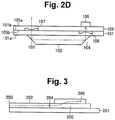
- this light receiving device As shown in Fig. 3 , light enters from an input end 203 of a semiconductor optical amplifier 202 formed on a substrate 201, and the incident light is amplified by the semiconductor optical amplifier 202 and is output from an outgoing end 204.
- the amplified light exiting the outgoing end 204 is guided by an optical waveguide 205 and enters into a photodiode 206.
- the light receiving device described above can take advantage of the amplification effect of the semiconductor optical amplifier and therefore can maintain a high light receiving sensitivity as the whole light receiving device even if the thickness of the absorption layer of the photodiode is reduced in order to increase speed.
- the semiconductor optical amplifier achieves an optical amplification of about 8 dB when the driving current is 170 mA.
- Non-Patent Literature 1 F. Xia et al., "Monolithic Integration of a Semiconductor Optical Amplifier and a High Bandwidth p-i-n Photodiode Using Asymmetric Twin-Waveguide Technology", IEEE Photonics Technology Letters, vol. 15, no. 3, pp. 452-454, 2003 .
- the technique described above has a problem of high manufacturing cost.
- the compound semiconductor layers to form the semiconductor optical amplifier are formed by crystal growth, and the compound semiconductor layers to form the photodiode are formed by crystal growth.
- the compound semiconductor layers to form the semiconductor optical amplifier and the compound semiconductor layers to form the photodiode are significantly different in manufacturing conditions, such as those concerning the crystal growth. Therefore, the manufacturing cost is high from the viewpoint of yield, such as evenness of the substrate surface.
- the present invention has been devised to solve the problem described above, and an object of the present invention is to inhibit an increase of the manufacturing cost of a light receiving device including a photodiode and a semiconductor optical amplifier.
- a light receiving device includes: a waveguide semiconductor optical amplifier that is formed on a principal surface of a first substrate and guides a wave in a direction parallel to the principal surface; a first reflection portion formed by an end face at one end of the semiconductor optical amplifier, the end face being formed to be oblique to the principal surface of the first substrate such that input light that is input to a back surface of the first substrate is to be input; a second reflection portion from which output light is to be output toward the back surface of the first substrate, the second reflection portion being formed by an end face at another end of the semiconductor optical amplifier, and the end face being formed to be oblique to the principal surface of the first substrate; a second substrate having a back surface bonded to the back surface of the first substrate; and a planar photodiode formed on a principal surface of the second substrate at a location where the photodiode is capable of receiving the output light output from the second reflection portion.
- the light receiving device described above may further include: a first condenser lens formed on the back surface of the first substrate or the back surface of the second substrate in an optical path of the input light that is input to the first reflection portion; and a second condenser lens formed on the back surface of the first substrate or the back surface of the second substrate in an optical path of the output light that is output from the second reflection portion and input to the photodiode.
- a method of manufacturing a light receiving device includes: a first step of forming, on a principal surface of a first substrate, a waveguide semiconductor optical amplifier that guides a wave in a direction parallel to the principal surface; a second step of forming a planar photodiode on a principal surface of a second substrate; and a third step of bonding a back surface of the first substrate and a back surface of the second substrate to each other, a first reflection portion is formed by an end face at one end of the semiconductor optical amplifier, the end face being formed to be oblique to the principal surface of the first substrate such that input light that is input to the back surface of the first substrate is to be input, a second reflection portion formed by an end face at the other end of the semiconductor optical amplifier, the end face being formed to be oblique to the principal surface of the first substrate such that output light is to be output toward the back surface of the first substrate, and the photodiode is formed on a principal surface of the second substrate at a location where the photodi
- the method of manufacturing a light receiving device described above may further include: a fourth step of forming a first condenser lens on the back surface of the first substrate or the back surface of the second substrate in an optical path of the input light that is input to the first reflection portion; and a fifth step of forming a second condenser lens on the back surface of the first substrate or the back surface of the second substrate in an optical path of the output light that is output from the second reflection portion and input to the photodiode.
- the present invention described above has a noticeable effect that an increase of the manufacturing cost of a light receiving device including a photodiode and a semiconductor optical amplifier can be inhibited.
- Fig. 1 is a schematic cross-sectional view.
- the light receiving device includes a semiconductor optical amplifier 102 formed on a principal surface 101a of a first substrate 101.
- the semiconductor optical amplifier 102 is a well-known waveguide semiconductor optical amplifier and guides light in a direction parallel to the principal surface 101a.
- the semiconductor optical amplifier 102 includes, for example, an n-type InP layer formed on the first substrate 101 made of InP, which is semi-insulating, an active layer as a gain medium made of InGaAsP, and a p-type InP layer formed on the active layer.
- An electrode is connected to each of the first substrate 101 and the p-type InP layer so that a current can be injected into the active layer.
- the semiconductor optical amplifier 102 includes a first reflection portion 103 at one end thereof, and the first reflection portion 103 is formed by an end face of the semiconductor optical amplifier 102 that is oblique to the principal surface 101a of the first substrate 101.
- the first reflection portion 103 allows input light input from the side of a back surface 101b of the first substrate 101 to enter.
- the semiconductor optical amplifier 102 further includes a second reflection portion 104 at another end thereof, and the second reflection portion 104 is formed by an end face of the semiconductor optical amplifier 102 that is oblique to the principal surface 101a of the first substrate 101. Output light amplified by the semiconductor optical amplifier 102 is output from the second reflection portion 104 to the side of the back surface 101b of the first substrate 101.
- the light receiving device further includes a second substrate 105 bonded to the back surface 101b of the first substrate 101 at a back surface 105b thereof and a photodiode 106 formed on a principal surface 105a of the second substrate 105.
- the photodiode 106 is a well-known planar (surface-incident) Pin-type photodiode.
- the photodiode 106 may be an avalanche photodiode.
- the photodiode 106 is formed at a location where the photodiode 106 can receive the output light from the second reflection portion 104.
- the waveguide semiconductor optical amplifier 102 that guides a wave in the direction parallel to the principal surface 101a is formed on the principal surface 101a of the first substrate 101 (a first step).
- the planar photodiode 106 is formed on the principal surface 105a of the second substrate 105 (a second step).
- the back surface 101b of the first substrate 101 and the back surface 105b of the second substrate 105 are bonded to each other (a third step).
- each element structure may be formed.
- the first substrate 101 and the second substrate 105 may be bonded to each other after the element structure of the semiconductor optical amplifier 102 and the element structure of the photodiode 106 are formed.
- the first substrate 101 made of semi-insulating InP is prepared, and semiconductor layers to form the semiconductor optical amplifier 102, such as an n-InP layer, an InGaAsP layer and a p-InP layer, are formed on the principal surface 101a of the first substrate 101 by epitaxial growth in a well-known organic metal vapor deposition process or the like.
- semiconductor layers to form the semiconductor optical amplifier 102 such as an n-InP layer, an InGaAsP layer and a p-InP layer, are formed on the principal surface 101a of the first substrate 101 by epitaxial growth in a well-known organic metal vapor deposition process or the like.
- the second substrate 105 made of semi-insulating InP is prepared, and semiconductor layers to form the photodiode 106, such as an n-InP layer, an InGaAs absorption layer and a p-InP layer, are formed on the principal surface 105a of the second substrate 105 by epitaxial growth in an organic metal vapor deposition process or the like.
- the first substrate 101 and the second substrate 105 are then each thinned to a predetermined thickness by grinding and polishing, and the back surface 101b of the first substrate 101 and the back surface 105b of the second substrate 105 are bonded to each other.
- the bonding described above can be achieved by a bonding technique, such as atomic diffusion bonding (ADB) or surface-activated bonding (SAB).
- ADB atomic diffusion bonding
- SAB surface-activated bonding
- the bonding described above may be achieved with an adhesive.
- the semiconductor layers formed on the principal surface 101a of the first substrate 101 are then patterned by a well-known photolithography technique or etching technique to form a waveguide structure (see Non-Patent Literature 1).
- the first reflection portion 103 and the second reflection portion 104 are formed.
- the waveguide structure formed has one end and another end shaped to be inclined by 45° with respect to the principal surface 101a of the first substrate 101.
- the angle of inclination of the reflection surface of the second reflection portion 104 may be different from 45° by several degrees.
- each electrode is formed in a well-known lift-off process or the like to complete the semiconductor optical amplifier 102.
- the semiconductor layers formed on the principal surface 105a of the second substrate 105 are patterned by a well-known photolithography technique or etching technique to form a mesa structure.
- Each electrode is formed in a well-known lift-off process or the like to complete the photodiode 106.
- the photodiode 106 is formed on the principal surface 105a of the second substrate 105 at a location where the photodiode 106 can receive the output light from the second reflection portion 104.
- the photodiode 106 is arranged on the principal surface 105a so that the output light from the second reflection portion 104 enters into the center of a light receiving surface of the photodiode 106.
- the location where the photodiode 106 is arranged depends on the angle of the reflection surface of the second reflection portion 104 and the thicknesses of the first substrate 101 and the second substrate 105.
- light first enters from the side of the principal surface 105a of the second substrate 105 and is transmitted through the second substrate 105 and the first substrate 101 to reach the first reflection portion 103.
- the light having reached the first reflection portion 103 changes the direction of travel, enters an amplification portion of the semiconductor optical amplifier 102 and is amplified.
- the amplified light amplified by the semiconductor optical amplifier 102 changes the direction of travel at the second reflection portion 104, is transmitted through the first substrate 101 and the second substrate 105, and is received and converted into electricity by the photodiode 106.
- the planar optical filter may be a thin-film filter (TFF) that is an optical DEMUX filter commonly used for a small receiver (ROSA) ready for wavelength division multiplexing (WDM) for optical communication, for example.
- TCF thin-film filter
- ROSA small receiver
- WDM wavelength division multiplexing
- Figs. 2A, 2B, 2C and 2D are schematic cross-sectional views.
- the light receiving device includes a semiconductor optical amplifier 102 formed on a principal surface 101a of a first substrate 101.
- the light receiving device further includes a second substrate 105 bonded to a back surface 101b of the first substrate 101 at a back surface 105b thereof and a photodiode 106 formed on a principal surface 105a of the second substrate 105.
- the configuration described so far is the same as the configuration of the light receiving device according to the first embodiment described earlier.
- the light receiving device includes a first condenser lens 107 formed on the back surface 101b of the first substrate 101 or the back surface 105b of the second substrate 105.
- the first condenser lens 107 is arranged on an optical path of input light that is input to the first reflection portion 103.
- the light receiving device further includes a second condenser lens 108 formed on the back surface 101b of the first substrate 101 or the back surface 105b of the second substrate 105.
- the second condenser lens 108 is arranged on an optical path of output light that is output from the second reflection portion 104 and input to the photodiode 106.
- the first condenser lens 107 can be formed on the back surface 101b of the first substrate 101, and the second condenser lens 108 can be formed on the back surface 105b of the second substrate 105.
- the first condenser lens 107 and the second condenser lens 108 can be formed on the back surface 101b of the first substrate 101.
- the first condenser lens 107 and the second condenser lens 108 can be formed on the back surface 105b of the second substrate 105. Forming the first condenser lens 107 and the second condenser lens 108 on one of the substrates allows a plurality of lens structures to be formed at the same time, which leads to a simplification of the process.
- the second condenser lens 108 may be formed on the back surface 101b of the first substrate 101, and the first condenser lens 107 may be formed on the back surface 105b of the second substrate 105.
- the first condenser lens 107 is formed on the back surface 101b of the first substrate 101 or the back surface 105b of the second substrate 105 in such a manner that the first condenser lens 107 is located on the optical path of the input light that is input to the first reflection portion 103 (a fourth step).
- the second condenser lens 108 is formed on the back surface 101b of the first substrate 101 or the back surface 105b of the second substrate 105 in such a manner that the second condenser lens 108 is located on the optical path of the output light that is output from the second reflection portion 104 and input to the photodiode 106 (a fifth step).
- the first substrate 101 made of semi-insulating InP is prepared, and a first mark for alignment is formed on the principal surface 101a.
- a first mark made of metal can be formed at a predetermined location in the lift-off process or the like.
- Semiconductor layers to form the semiconductor optical amplifier 102 such as an n-InP layer, an InGaAsP layer and a p-InP layer, are then formed on the principal surface 101a of the first substrate 101 by epitaxial growth in a well-known organic metal vapor deposition process or the like.
- the second substrate 105 made of semi-insulating InP is prepared, and a second mark for alignment is formed on the principal surface 101a.
- Semiconductor layers to form the photodiode 106 such as an n-InP layer, an InGaAs absorption layer and a p-InP layer, are then formed on the principal surface 105a of the second substrate 105 by epitaxial growth in an organic metal vapor deposition process or the like.
- the first substrate 101 and the second substrate 105 are then each thinned to a predetermined thickness by grinding and polishing.
- the first condenser lens 107 is formed on the back surface 101b of the first substrate 101 in this state.
- a recess having a convex surface at the bottom thereof is formed in the back surface 101b of the first substrate 101, and the recess serves as the first condenser lens 107.
- the second condenser lens 108 is formed on the back surface 105b of the second substrate 105 in the same manner.
- the first condenser lens 107 is formed at a predetermined location with reference to the first mark
- the second condenser lens 108 is formed at a predetermined location with reference to the second mark.
- the first condenser lens 107 and the second condenser lens 108 may be formed on the back surface of one of the substrates.
- the back surface 101b of the first substrate 101 and the back surface 105b of the second substrate 105 are bonded to each other.
- the bonding described above can be achieved by a bonding technique, such as atomic diffusion bonding (ADB) or surface-activated bonding (SAB).
- ADB atomic diffusion bonding
- SAB surface-activated bonding
- the bonding described above may be achieved with an adhesive. In the bonding, it is to be ensured that the first mark and the second mark are in a predetermined positional relationship.
- the recess of the first condenser lens 107 and the recess of the second condenser lens 108 may be a space (an air layer) or may be filled with a dielectric, such as silicon oxide.
- a large difference in index of refraction can be provided between the first substrate 101 and the second substrate 105, which are made of InP, and the air layer or dielectric layer in the recesses described above, and the condenser lens can be provided by the convex surface at the bottom of the recess.
- an antireflection film designed according to the properties of the material of the recess may be formed on the front surface of the condenser lens and the back surface of the first substrate or second substrate.
- an antireflection film may be formed on the principal surface 105a of the second substrate 105 in a part into which the light enters.
- the semiconductor layers formed on the principal surface 101a of the first substrate 101 are then patterned to form a waveguide structure.
- the first reflection portion 103 and the second reflection portion 104 are formed.
- each electrode is formed in a well-known lift-off process or the like to complete the semiconductor optical amplifier 102.
- the semiconductor optical amplifier 102 is formed to be in a predetermined positional relationship with the first mark.
- the semiconductor layers formed on the principal surface 105a of the second substrate 105 are patterned to form a mesa structure.
- Each electrode is formed in a well-known lift-off process or the like to complete the photodiode 106.
- the photodiode 106 is formed to be in a predetermined positional relationship with the second mark.
- the first condenser lens 107 is arranged on the optical path of the input light that is input to the first reflection portion 103.
- the photodiode 106 is formed on the principal surface 105a of the second substrate 105 at a location where the photodiode 106 can receive the output light that is output from the second reflection portion 104, and the second condenser lens 108 is arranged on the optical path of the output light.
- the first condenser lens 107 and the second condenser lens 108 are provided. These lenses provide advantages that the degree of flexibility in thickness of the first substrate 101 and the second substrate 105 is increased, and the manufacturing margin is improved so that the manufacturing cost is reduced. In addition, since the light is introduced through the first condenser lens 107, the light receiving device according to the second embodiment has an improved packaging tolerance and contributes to a reduction of the cost of the fabrication of a receiver module.
- the semiconductor optical amplifier and the photodiode are formed on the first substrate and the second substrate, respectively, which are bonded to each other, an increase of the cost of manufacturing the light receiving device including the photodiode and the semiconductor optical amplifier can be inhibited.
- the semiconductor layers to form the semiconductor optical amplifier and the semiconductor layers to form the photodiode can be separately formed, so that an optical formation (crystal growth) condition for each of the elements can be adopted.
- the light receiving device according to the present invention can be of a planar type, which permits vertical incidence of light, the optical coupling tolerance is increased, and the light receiving device can be more easily implemented.
- the first condenser lens and the second condenser lens are provided, the optical coupling tolerance can be further increased.
Landscapes
- Physics & Mathematics (AREA)
- General Physics & Mathematics (AREA)
- Optics & Photonics (AREA)
- Light Receiving Elements (AREA)
- Electroluminescent Light Sources (AREA)
Abstract
Description
- The present invention relates to a light receiving device including a photodiode and a semiconductor optical amplifier, and a method of manufacturing the same.
- In recent years, as the communication capacity of data centers or the like is increasing, there is a demand for increased speed of a photodiode (PD), which is a photoelectric conversion element incorporated in a receiver. As an approach to increase the speed, there is a technique of reducing the thickness of the absorption layer and thereby reducing the time of travel of carriers generated by reception of light. However, this technique leads to a decrease in light receiving sensitivity because the thickness of the absorption layers is reduced. In this way, there is a trade-off relationship between the increase in speed and the light receiving sensitivity.
- As described above, it is difficult for a photodiode to achieve a high speed and a high light receiving sensitivity at the same time by itself. However, there is a technique of improving the light receiving sensitivity while ensuring a high speed by integrating a photodiode with a semiconductor optical amplifier (see Non-Patent Literature 1).
- According to the technique, a semiconductor optical amplifier and a photodiode are formed on a principal surface of a substrate made of InP. In this technique, on the InP substrate, compound semiconductor layers to form the semiconductor optical amplifier are first formed by crystal growth, and compound semiconductor layers to form the photodiode are then formed by crystal growth. These compound semiconductor layers formed by crystal growth are then patterned into a predetermined shape, thereby forming a light receiving device including a waveguide semiconductor optical amplifier and a photodiode (see
Fig. 1 of Non-Patent Literature 1). - With this light receiving device, as shown in
Fig. 3 , light enters from aninput end 203 of a semiconductoroptical amplifier 202 formed on asubstrate 201, and the incident light is amplified by the semiconductoroptical amplifier 202 and is output from anoutgoing end 204. The amplified light exiting theoutgoing end 204 is guided by anoptical waveguide 205 and enters into aphotodiode 206. - Unlike the photodiode that receives light only by itself, the light receiving device described above can take advantage of the amplification effect of the semiconductor optical amplifier and therefore can maintain a high light receiving sensitivity as the whole light receiving device even if the thickness of the absorption layer of the photodiode is reduced in order to increase speed. According to Non-Patent Literature 1, the semiconductor optical amplifier achieves an optical amplification of about 8 dB when the driving current is 170 mA.
- Non-Patent Literature 1: F. Xia et al., "Monolithic Integration of a Semiconductor Optical Amplifier and a High Bandwidth p-i-n Photodiode Using Asymmetric Twin-Waveguide Technology", IEEE Photonics Technology Letters, vol. 15, no. 3, pp. 452-454, 2003.
- However, the technique described above has a problem of high manufacturing cost. As described above, the compound semiconductor layers to form the semiconductor optical amplifier are formed by crystal growth, and the compound semiconductor layers to form the photodiode are formed by crystal growth. However, the compound semiconductor layers to form the semiconductor optical amplifier and the compound semiconductor layers to form the photodiode are significantly different in manufacturing conditions, such as those concerning the crystal growth. Therefore, the manufacturing cost is high from the viewpoint of yield, such as evenness of the substrate surface.
- The present invention has been devised to solve the problem described above, and an object of the present invention is to inhibit an increase of the manufacturing cost of a light receiving device including a photodiode and a semiconductor optical amplifier.
- A light receiving device according to the present invention includes: a waveguide semiconductor optical amplifier that is formed on a principal surface of a first substrate and guides a wave in a direction parallel to the principal surface; a first reflection portion formed by an end face at one end of the semiconductor optical amplifier, the end face being formed to be oblique to the principal surface of the first substrate such that input light that is input to a back surface of the first substrate is to be input; a second reflection portion from which output light is to be output toward the back surface of the first substrate, the second reflection portion being formed by an end face at another end of the semiconductor optical amplifier, and the end face being formed to be oblique to the principal surface of the first substrate; a second substrate having a back surface bonded to the back surface of the first substrate; and a planar photodiode formed on a principal surface of the second substrate at a location where the photodiode is capable of receiving the output light output from the second reflection portion.
- The light receiving device described above may further include: a first condenser lens formed on the back surface of the first substrate or the back surface of the second substrate in an optical path of the input light that is input to the first reflection portion; and a second condenser lens formed on the back surface of the first substrate or the back surface of the second substrate in an optical path of the output light that is output from the second reflection portion and input to the photodiode.
- A method of manufacturing a light receiving device according to the present invention includes: a first step of forming, on a principal surface of a first substrate, a waveguide semiconductor optical amplifier that guides a wave in a direction parallel to the principal surface; a second step of forming a planar photodiode on a principal surface of a second substrate; and a third step of bonding a back surface of the first substrate and a back surface of the second substrate to each other, a first reflection portion is formed by an end face at one end of the semiconductor optical amplifier, the end face being formed to be oblique to the principal surface of the first substrate such that input light that is input to the back surface of the first substrate is to be input, a second reflection portion formed by an end face at the other end of the semiconductor optical amplifier, the end face being formed to be oblique to the principal surface of the first substrate such that output light is to be output toward the back surface of the first substrate, and the photodiode is formed on a principal surface of the second substrate at a location where the photodiode is capable of receiving the output light output from the second reflection portion.
- The method of manufacturing a light receiving device described above may further include: a fourth step of forming a first condenser lens on the back surface of the first substrate or the back surface of the second substrate in an optical path of the input light that is input to the first reflection portion; and a fifth step of forming a second condenser lens on the back surface of the first substrate or the back surface of the second substrate in an optical path of the output light that is output from the second reflection portion and input to the photodiode.
- The present invention described above has a noticeable effect that an increase of the manufacturing cost of a light receiving device including a photodiode and a semiconductor optical amplifier can be inhibited.
-
- [
Fig. 1] Fig. 1 is a diagram showing a configuration of a light receiving device according to a first embodiment of the present invention. - [
Fig. 2A] Fig. 2A is a diagram showing a configuration of a light receiving device according to a second embodiment of the present invention. - [
Fig. 2B] Fig. 2B is a diagram showing another configuration of the light receiving device according to the second embodiment of the present invention. - [
Fig. 2C] Fig. 2C is a diagram showing another configuration of the light receiving device according to the second embodiment of the present invention. - [
Fig. 2D] Fig. 2D is a diagram showing another configuration of the light receiving device according to the second embodiment of the present invention. - [
Fig. 3] Fig. 3 is a diagram showing a configuration of a conventional light receiving device. - In the following, light receiving devices according to embodiments of the present invention will be described.
- First, a light receiving device according to a first embodiment of the present invention will be described with reference to
Fig. 1. Fig. 1 is a schematic cross-sectional view. - The light receiving device includes a semiconductor
optical amplifier 102 formed on aprincipal surface 101a of afirst substrate 101. The semiconductoroptical amplifier 102 is a well-known waveguide semiconductor optical amplifier and guides light in a direction parallel to theprincipal surface 101a. The semiconductoroptical amplifier 102 includes, for example, an n-type InP layer formed on thefirst substrate 101 made of InP, which is semi-insulating, an active layer as a gain medium made of InGaAsP, and a p-type InP layer formed on the active layer. An electrode is connected to each of thefirst substrate 101 and the p-type InP layer so that a current can be injected into the active layer. - The semiconductor
optical amplifier 102 includes afirst reflection portion 103 at one end thereof, and thefirst reflection portion 103 is formed by an end face of the semiconductoroptical amplifier 102 that is oblique to theprincipal surface 101a of thefirst substrate 101. Thefirst reflection portion 103 allows input light input from the side of aback surface 101b of thefirst substrate 101 to enter. - The semiconductor
optical amplifier 102 further includes asecond reflection portion 104 at another end thereof, and thesecond reflection portion 104 is formed by an end face of the semiconductoroptical amplifier 102 that is oblique to theprincipal surface 101a of thefirst substrate 101. Output light amplified by the semiconductoroptical amplifier 102 is output from thesecond reflection portion 104 to the side of theback surface 101b of thefirst substrate 101. - The light receiving device further includes a
second substrate 105 bonded to theback surface 101b of thefirst substrate 101 at aback surface 105b thereof and aphotodiode 106 formed on aprincipal surface 105a of thesecond substrate 105. Thephotodiode 106 is a well-known planar (surface-incident) Pin-type photodiode. Thephotodiode 106 may be an avalanche photodiode. Thephotodiode 106 is formed at a location where thephotodiode 106 can receive the output light from thesecond reflection portion 104. - Next, a method of manufacturing the light receiving device according to the first embodiment will be described. In this manufacturing method, the waveguide semiconductor
optical amplifier 102 that guides a wave in the direction parallel to theprincipal surface 101a is formed on theprincipal surface 101a of the first substrate 101 (a first step). Theplanar photodiode 106 is formed on theprincipal surface 105a of the second substrate 105 (a second step). Theback surface 101b of thefirst substrate 101 and theback surface 105b of thesecond substrate 105 are bonded to each other (a third step). - Alternatively, after the semiconductor layers to form the semiconductor
optical amplifier 102 are formed, the semiconductors to form thephotodiode 106 are formed, and the substrates are then bonded to each other, each element structure may be formed. Alternatively, thefirst substrate 101 and thesecond substrate 105 may be bonded to each other after the element structure of the semiconductoroptical amplifier 102 and the element structure of thephotodiode 106 are formed. - For example, the
first substrate 101 made of semi-insulating InP is prepared, and semiconductor layers to form the semiconductoroptical amplifier 102, such as an n-InP layer, an InGaAsP layer and a p-InP layer, are formed on theprincipal surface 101a of thefirst substrate 101 by epitaxial growth in a well-known organic metal vapor deposition process or the like. - On the other hand, the
second substrate 105 made of semi-insulating InP is prepared, and semiconductor layers to form thephotodiode 106, such as an n-InP layer, an InGaAs absorption layer and a p-InP layer, are formed on theprincipal surface 105a of thesecond substrate 105 by epitaxial growth in an organic metal vapor deposition process or the like. - The
first substrate 101 and thesecond substrate 105 are then each thinned to a predetermined thickness by grinding and polishing, and theback surface 101b of thefirst substrate 101 and theback surface 105b of thesecond substrate 105 are bonded to each other. The bonding described above can be achieved by a bonding technique, such as atomic diffusion bonding (ADB) or surface-activated bonding (SAB). Alternatively, the bonding described above may be achieved with an adhesive. - The semiconductor layers formed on the
principal surface 101a of thefirst substrate 101 are then patterned by a well-known photolithography technique or etching technique to form a waveguide structure (see Non-Patent Literature 1). By this patterning, thefirst reflection portion 103 and thesecond reflection portion 104 are formed. For example, the waveguide structure formed has one end and another end shaped to be inclined by 45° with respect to theprincipal surface 101a of thefirst substrate 101. In order to prevent light that has failed to be absorbed by thephotodiode 106 from returning to the semiconductoroptical amplifier 102, the angle of inclination of the reflection surface of thesecond reflection portion 104 may be different from 45° by several degrees. - After the waveguide structure is formed as described above, each electrode is formed in a well-known lift-off process or the like to complete the semiconductor
optical amplifier 102. - On the other hand, the semiconductor layers formed on the
principal surface 105a of thesecond substrate 105 are patterned by a well-known photolithography technique or etching technique to form a mesa structure. Each electrode is formed in a well-known lift-off process or the like to complete thephotodiode 106. - The
photodiode 106 is formed on theprincipal surface 105a of thesecond substrate 105 at a location where thephotodiode 106 can receive the output light from thesecond reflection portion 104. In particular, thephotodiode 106 is arranged on theprincipal surface 105a so that the output light from thesecond reflection portion 104 enters into the center of a light receiving surface of thephotodiode 106. The location where thephotodiode 106 is arranged depends on the angle of the reflection surface of thesecond reflection portion 104 and the thicknesses of thefirst substrate 101 and thesecond substrate 105. - With the light receiving device according to the first embodiment, light first enters from the side of the
principal surface 105a of thesecond substrate 105 and is transmitted through thesecond substrate 105 and thefirst substrate 101 to reach thefirst reflection portion 103. The light having reached thefirst reflection portion 103 changes the direction of travel, enters an amplification portion of the semiconductoroptical amplifier 102 and is amplified. The amplified light amplified by the semiconductoroptical amplifier 102 changes the direction of travel at thesecond reflection portion 104, is transmitted through thefirst substrate 101 and thesecond substrate 105, and is received and converted into electricity by thephotodiode 106. - According to the first embodiment, light enters into the substrate in a direction substantially perpendicular to the substrate surface, so that the light receiving device can be easily combined with a planar optical filter or the like. The planar optical filter may be a thin-film filter (TFF) that is an optical DEMUX filter commonly used for a small receiver (ROSA) ready for wavelength division multiplexing (WDM) for optical communication, for example.
- Next, a light receiving device according to a second embodiment of the present invention will be described with reference to
Figs. 2A, 2B, 2C and2D .Figs. 2A, 2B, 2C and2D are schematic cross-sectional views. - The light receiving device includes a semiconductor
optical amplifier 102 formed on aprincipal surface 101a of afirst substrate 101. The light receiving device further includes asecond substrate 105 bonded to aback surface 101b of thefirst substrate 101 at aback surface 105b thereof and aphotodiode 106 formed on aprincipal surface 105a of thesecond substrate 105. The configuration described so far is the same as the configuration of the light receiving device according to the first embodiment described earlier. - The light receiving device according to the second embodiment includes a
first condenser lens 107 formed on theback surface 101b of thefirst substrate 101 or theback surface 105b of thesecond substrate 105. Thefirst condenser lens 107 is arranged on an optical path of input light that is input to thefirst reflection portion 103. The light receiving device further includes asecond condenser lens 108 formed on theback surface 101b of thefirst substrate 101 or theback surface 105b of thesecond substrate 105. Thesecond condenser lens 108 is arranged on an optical path of output light that is output from thesecond reflection portion 104 and input to thephotodiode 106. - For example, as shown in
Fig. 2A , thefirst condenser lens 107 can be formed on theback surface 101b of thefirst substrate 101, and thesecond condenser lens 108 can be formed on theback surface 105b of thesecond substrate 105. Alternatively, as shown inFig. 2B , thefirst condenser lens 107 and thesecond condenser lens 108 can be formed on theback surface 101b of thefirst substrate 101. Alternatively, as shown inFig. 2C , thefirst condenser lens 107 and thesecond condenser lens 108 can be formed on theback surface 105b of thesecond substrate 105. Forming thefirst condenser lens 107 and thesecond condenser lens 108 on one of the substrates allows a plurality of lens structures to be formed at the same time, which leads to a simplification of the process. - Alternatively, as shown in
Fig. 2D , thesecond condenser lens 108 may be formed on theback surface 101b of thefirst substrate 101, and thefirst condenser lens 107 may be formed on theback surface 105b of thesecond substrate 105. - Next, a method of manufacturing the light receiving device according to the second embodiment will be described. In the second embodiment, in addition to the elements formed in the manufacturing method according to the first embodiment described earlier, the
first condenser lens 107 is formed on theback surface 101b of thefirst substrate 101 or theback surface 105b of thesecond substrate 105 in such a manner that thefirst condenser lens 107 is located on the optical path of the input light that is input to the first reflection portion 103 (a fourth step). In addition, thesecond condenser lens 108 is formed on theback surface 101b of thefirst substrate 101 or theback surface 105b of thesecond substrate 105 in such a manner that thesecond condenser lens 108 is located on the optical path of the output light that is output from thesecond reflection portion 104 and input to the photodiode 106 (a fifth step). - For example, the
first substrate 101 made of semi-insulating InP is prepared, and a first mark for alignment is formed on theprincipal surface 101a. For example, a first mark made of metal can be formed at a predetermined location in the lift-off process or the like. Semiconductor layers to form the semiconductoroptical amplifier 102, such as an n-InP layer, an InGaAsP layer and a p-InP layer, are then formed on theprincipal surface 101a of thefirst substrate 101 by epitaxial growth in a well-known organic metal vapor deposition process or the like. - On the other hand, the
second substrate 105 made of semi-insulating InP is prepared, and a second mark for alignment is formed on theprincipal surface 101a. Semiconductor layers to form thephotodiode 106, such as an n-InP layer, an InGaAs absorption layer and a p-InP layer, are then formed on theprincipal surface 105a of thesecond substrate 105 by epitaxial growth in an organic metal vapor deposition process or the like. - The
first substrate 101 and thesecond substrate 105 are then each thinned to a predetermined thickness by grinding and polishing. Thefirst condenser lens 107 is formed on theback surface 101b of thefirst substrate 101 in this state. For example, a recess having a convex surface at the bottom thereof is formed in theback surface 101b of thefirst substrate 101, and the recess serves as thefirst condenser lens 107. Thesecond condenser lens 108 is formed on theback surface 105b of thesecond substrate 105 in the same manner. Thefirst condenser lens 107 is formed at a predetermined location with reference to the first mark, and thesecond condenser lens 108 is formed at a predetermined location with reference to the second mark. Alternatively, thefirst condenser lens 107 and thesecond condenser lens 108 may be formed on the back surface of one of the substrates. - After the
first condenser lens 107 and thesecond condenser lens 108 are formed as described above, theback surface 101b of thefirst substrate 101 and theback surface 105b of thesecond substrate 105 are bonded to each other. The bonding described above can be achieved by a bonding technique, such as atomic diffusion bonding (ADB) or surface-activated bonding (SAB). Alternatively, the bonding described above may be achieved with an adhesive. In the bonding, it is to be ensured that the first mark and the second mark are in a predetermined positional relationship. - The recess of the
first condenser lens 107 and the recess of thesecond condenser lens 108 may be a space (an air layer) or may be filled with a dielectric, such as silicon oxide. A large difference in index of refraction can be provided between thefirst substrate 101 and thesecond substrate 105, which are made of InP, and the air layer or dielectric layer in the recesses described above, and the condenser lens can be provided by the convex surface at the bottom of the recess. Furthermore, in order to prevent a reflection loss of the input light and the output light, an antireflection film designed according to the properties of the material of the recess may be formed on the front surface of the condenser lens and the back surface of the first substrate or second substrate. Furthermore, in order to prevent a reflection loss of the input light, an antireflection film may be formed on theprincipal surface 105a of thesecond substrate 105 in a part into which the light enters. - As in the first embodiment described earlier, the semiconductor layers formed on the
principal surface 101a of thefirst substrate 101 are then patterned to form a waveguide structure. By this patterning, thefirst reflection portion 103 and thesecond reflection portion 104 are formed. Furthermore, after the waveguide structure is formed as described above, each electrode is formed in a well-known lift-off process or the like to complete the semiconductoroptical amplifier 102. In the second embodiment, the semiconductoroptical amplifier 102 is formed to be in a predetermined positional relationship with the first mark. - As in the first embodiment described earlier, the semiconductor layers formed on the
principal surface 105a of thesecond substrate 105 are patterned to form a mesa structure. Each electrode is formed in a well-known lift-off process or the like to complete thephotodiode 106. In the second embodiment, thephotodiode 106 is formed to be in a predetermined positional relationship with the second mark. - By forming the
first condenser lens 107, thesecond condenser lens 108, the semiconductoroptical amplifier 102 and thephotodiode 106 in such a manner that each of them is in a predetermined positional relationship with the first mark or second mark as described above, thefirst condenser lens 107 is arranged on the optical path of the input light that is input to thefirst reflection portion 103. In addition, thephotodiode 106 is formed on theprincipal surface 105a of thesecond substrate 105 at a location where thephotodiode 106 can receive the output light that is output from thesecond reflection portion 104, and thesecond condenser lens 108 is arranged on the optical path of the output light. - According to the second embodiment, the
first condenser lens 107 and thesecond condenser lens 108 are provided. These lenses provide advantages that the degree of flexibility in thickness of thefirst substrate 101 and thesecond substrate 105 is increased, and the manufacturing margin is improved so that the manufacturing cost is reduced. In addition, since the light is introduced through thefirst condenser lens 107, the light receiving device according to the second embodiment has an improved packaging tolerance and contributes to a reduction of the cost of the fabrication of a receiver module. - As described above, since the semiconductor optical amplifier and the photodiode are formed on the first substrate and the second substrate, respectively, which are bonded to each other, an increase of the cost of manufacturing the light receiving device including the photodiode and the semiconductor optical amplifier can be inhibited. According to the present invention, the semiconductor layers to form the semiconductor optical amplifier and the semiconductor layers to form the photodiode can be separately formed, so that an optical formation (crystal growth) condition for each of the elements can be adopted. In addition, since the light receiving device according to the present invention can be of a planar type, which permits vertical incidence of light, the optical coupling tolerance is increased, and the light receiving device can be more easily implemented. In addition, since the first condenser lens and the second condenser lens are provided, the optical coupling tolerance can be further increased.
- It is obvious that the present invention is not limited to the embodiments described above, and those of ordinary skill in the art can contemplate many modifications and combinations within the technical concept of the present invention.
-
- 101
- First Substrate
- 101a
- Principal Surface
- 101b
- Back Surface
- 102
- Semiconductor Optical Amplifier
- 103
- First Reflection Portion
- 104
- Second Reflection Portion
- 105
- Second Substrate
- 105a
- Principal Surface
- 105b
- Back Surface
- 106
- Photodiode
Claims (4)
- A light receiving device, comprising:a waveguide semiconductor optical amplifier that is formed on a principal surface of a first substrate and guides a wave in a direction parallel to the principal surface;a first reflection portion formed by an end face at one end of the semiconductor optical amplifier, the end face being formed to be oblique to the principal surface of the first substrate such that input light that is input to a back surface of the first substrate is to be input;a second reflection portion formed by an end face at the other end of the semiconductor optical amplifier, the end face being formed to be oblique to the principal surface of the first substrate such that output light is to be output toward the back surface of the first substrate ;a second substrate having a back surface bonded to the back surface of the first substrate; anda planar photodiode formed on a principal surface of the second substrate at a location where the photodiode is capable of receiving the output light output from the second reflection portion.
- The light receiving device according to Claim 1, further comprising:a first condenser lens formed on the back surface of the first substrate or the back surface of the second substrate in an optical path of the input light that is input to the first reflection portion; anda second condenser lens formed on the back surface of the first substrate or the back surface of the second substrate in an optical path of the output light that is output from the second reflection portion and input to the photodiode.
- A method of manufacturing a light receiving device, comprising:a first step of forming, on a principal surface of a first substrate, a waveguide semiconductor optical amplifier that guides a wave in a direction parallel to the principal surface;a second step of forming a planar photodiode on a principal surface of a second substrate; anda third step of bonding a back surface of the first substrate and a back surface of the second substrate to each other,wherein a first reflection portion is formed by an end face at one end of the semiconductor optical amplifier, the end face being formed to be oblique to the principal surface of the first substrate such that input light that is input to the back surface of the first substrate is to be input,a second reflection portion formed by an end face at the other end of the semiconductor optical amplifier, the end face being formed to be oblique to the principal surface of the first substrate such that output light is to be output toward the back surface of the first substrate, andthe photodiode is formed on a principal surface of the second substrate at a location where the photodiode is capable of receiving the output light output from the second reflection portion.
- The method of manufacturing a light receiving device according to Claim 3, further comprising:a fourth step of forming a first condenser lens on the back surface of the first substrate or the back surface of the second substrate in an optical path of the input light that is input to the first reflection portion; anda fifth step of forming a second condenser lens on the back surface of the first substrate or the back surface of the second substrate in an optical path of the output light that is output from the second reflection portion and input to the photodiode.
Applications Claiming Priority (2)
| Application Number | Priority Date | Filing Date | Title |
|---|---|---|---|
| JP2018110045A JP6981370B2 (en) | 2018-06-08 | 2018-06-08 | Light receiving device and its manufacturing method |
| PCT/JP2019/019894 WO2019235199A1 (en) | 2018-06-08 | 2019-05-20 | Light receiving device and method of manufacturing same |
Publications (3)
| Publication Number | Publication Date |
|---|---|
| EP3806164A1 true EP3806164A1 (en) | 2021-04-14 |
| EP3806164A4 EP3806164A4 (en) | 2022-03-23 |
| EP3806164B1 EP3806164B1 (en) | 2023-12-27 |
Family
ID=68770257
Family Applications (1)
| Application Number | Title | Priority Date | Filing Date |
|---|---|---|---|
| EP19814316.6A Active EP3806164B1 (en) | 2018-06-08 | 2019-05-20 | Light receiving device and method of manufacturing same |
Country Status (5)
| Country | Link |
|---|---|
| US (1) | US11803017B2 (en) |
| EP (1) | EP3806164B1 (en) |
| JP (1) | JP6981370B2 (en) |
| CN (1) | CN112236871B (en) |
| WO (1) | WO2019235199A1 (en) |
Families Citing this family (2)
| Publication number | Priority date | Publication date | Assignee | Title |
|---|---|---|---|---|
| US20230091050A1 (en) * | 2021-09-20 | 2023-03-23 | Intel Corporation | Optical waveguides within a glass substrate to optically couple dies attached to the glass substrate |
| US12442985B2 (en) * | 2022-06-17 | 2025-10-14 | Taiwan Semiconductor Manufacturing Company Ltd. | Semiconductor structure and method of manufacturing the same |
Family Cites Families (24)
| Publication number | Priority date | Publication date | Assignee | Title |
|---|---|---|---|---|
| JPH05259504A (en) * | 1992-03-16 | 1993-10-08 | Hitachi Ltd | Semiconductor device |
| JPH1140823A (en) * | 1997-05-22 | 1999-02-12 | Fujitsu Ltd | Photodetector module |
| JPH1114832A (en) * | 1997-06-20 | 1999-01-22 | Nippon Telegr & Teleph Corp <Ntt> | Transparent optical substrate, optical interconnect integrated circuit device and method of manufacturing the same |
| KR100289040B1 (en) * | 1997-12-22 | 2001-05-02 | 이계철 | Bi-directional optical communication module using single optical fiber |
| JP3609251B2 (en) * | 1998-03-12 | 2005-01-12 | 日本電信電話株式会社 | Optical receiver |
| JP3594510B2 (en) * | 1999-04-01 | 2004-12-02 | 日本電信電話株式会社 | Optical module |
| JP2002141609A (en) * | 2000-11-02 | 2002-05-17 | Furukawa Electric Co Ltd:The | Semiconductor laser module, laser unit, and Raman amplifier |
| US6782028B2 (en) * | 2000-12-15 | 2004-08-24 | The Furukawa Electric Co., Ltd. | Semiconductor laser device for use in a semiconductor laser module and an optical amplifier |
| US7010183B2 (en) * | 2002-03-20 | 2006-03-07 | The Regents Of The University Of Colorado | Surface plasmon devices |
| US7177515B2 (en) * | 2002-03-20 | 2007-02-13 | The Regents Of The University Of Colorado | Surface plasmon devices |
| JP2003121889A (en) * | 2001-10-15 | 2003-04-23 | Fujitsu Ltd | Optical switch and optical demultiplexer |
| AU2003270519A1 (en) * | 2002-10-10 | 2004-05-04 | Xponent Photonics Inc. | Semiconductor photodetector with internal reflector |
| US7389013B2 (en) * | 2004-09-30 | 2008-06-17 | Stmicroelectronics, Inc. | Method and system for vertical optical coupling on semiconductor substrate |
| JP2008277445A (en) * | 2007-04-26 | 2008-11-13 | Opnext Japan Inc | Semiconductor laser and optical module |
| JP2010251649A (en) * | 2009-04-20 | 2010-11-04 | Hitachi Ltd | Surface emitting laser module and surface light receiving module |
| US8855160B2 (en) * | 2009-11-30 | 2014-10-07 | Hitachi, Ltd. | Horizontal-cavity surface-emitting laser |
| TWI446036B (en) * | 2010-05-24 | 2014-07-21 | Univ Nat Central | Optical transmission module |
| JP2012151157A (en) * | 2011-01-17 | 2012-08-09 | Hitachi Ltd | Horizontal resonator vertical emission laser, method of manufacturing the same, light receiving element, and horizontal resonator vertical emission laser array |
| JP2013228467A (en) * | 2012-04-24 | 2013-11-07 | Nippon Mektron Ltd | Opto-electric hybrid flexible print circuit board and manufacturing method thereof |
| JP5964143B2 (en) * | 2012-05-31 | 2016-08-03 | 日本メクトロン株式会社 | Manufacturing method of opto-electric hybrid printed wiring board |
| JP5892875B2 (en) * | 2012-06-22 | 2016-03-23 | Nttエレクトロニクス株式会社 | Optoelectronic integrated module |
| CN107111060A (en) * | 2014-07-14 | 2017-08-29 | 拜奥德光电公司 | With the 3D integreted phontonics of optical coupling element |
| FR3047811B1 (en) * | 2016-02-12 | 2018-03-16 | Commissariat A L'energie Atomique Et Aux Energies Alternatives | MODULATOR OF PROPAGATION LOSSES AND OF THE PROPAGATION INDEX OF A GUIDE OPTICAL SIGNAL |
| DE102016217749B4 (en) * | 2016-09-16 | 2023-07-06 | Sicoya Gmbh | Photonic device |
-
2018
- 2018-06-08 JP JP2018110045A patent/JP6981370B2/en active Active
-
2019
- 2019-05-20 EP EP19814316.6A patent/EP3806164B1/en active Active
- 2019-05-20 US US15/734,601 patent/US11803017B2/en active Active
- 2019-05-20 WO PCT/JP2019/019894 patent/WO2019235199A1/en not_active Ceased
- 2019-05-20 CN CN201980037600.6A patent/CN112236871B/en active Active
Also Published As
| Publication number | Publication date |
|---|---|
| CN112236871A (en) | 2021-01-15 |
| JP6981370B2 (en) | 2021-12-15 |
| EP3806164A4 (en) | 2022-03-23 |
| EP3806164B1 (en) | 2023-12-27 |
| JP2019212861A (en) | 2019-12-12 |
| US20210157070A1 (en) | 2021-05-27 |
| CN112236871B (en) | 2024-05-28 |
| US11803017B2 (en) | 2023-10-31 |
| WO2019235199A1 (en) | 2019-12-12 |
Similar Documents
| Publication | Publication Date | Title |
|---|---|---|
| US6104047A (en) | Avalanche photodiode with thin built-in depletion region | |
| US10468543B2 (en) | Microstructure enhanced absorption photosensitive devices | |
| US8269303B2 (en) | SiGe photodiode | |
| US20180102442A1 (en) | Microstructure enhanced absorption photosensitive devices | |
| US10199525B2 (en) | Light-receiving element and optical integrated circuit | |
| EP4207318B1 (en) | Avalanche photodetector and preparation method therefor | |
| US9978890B1 (en) | Germanium multi-directional detector | |
| US10374107B2 (en) | Optical waveguide integrated light receiving element and method of manufacturing the same | |
| WO2019089437A1 (en) | Microstructure enhanced absorption photosensitive devices | |
| US9406832B2 (en) | Waveguide-coupled MSM-type photodiode | |
| JP2011124450A (en) | Semiconductor light reception element | |
| US11803017B2 (en) | Light receiving device and method of manufacturing the same | |
| EP0452801A2 (en) | Semiconductor device having light receiving element and method of producing the same | |
| US11927814B2 (en) | Semiconductor photodetector array sensor integrated with optical-waveguide-based devices | |
| US11862739B2 (en) | Photoreceiver and optical receiver having an inclined surface | |
| JPH06268196A (en) | Optical integrated device | |
| KR101066604B1 (en) | Manufacturing method of avalanche photodiode | |
| KR100216524B1 (en) | Avalanche Photodiode and Manufacturing Method Thereof | |
| CN115425034A (en) | Photon integrated gain detector structure | |
| JPH04263475A (en) | Semiconductor photodetector and manufacture thereof | |
| JP6660282B2 (en) | Light receiving element | |
| CN117038773A (en) | A multi-channel photodetector based on micro-ring structure | |
| CN121285080A (en) | Monolithic optoelectronic integrated chip structure and manufacturing method thereof | |
| JPH02119273A (en) | Semiconductor photodetector | |
| KR19990015379A (en) | Photodetector element having wavelength division multiplexing function and manufacturing method thereof |
Legal Events
| Date | Code | Title | Description |
|---|---|---|---|
| STAA | Information on the status of an ep patent application or granted ep patent |
Free format text: STATUS: THE INTERNATIONAL PUBLICATION HAS BEEN MADE |
|
| PUAI | Public reference made under article 153(3) epc to a published international application that has entered the european phase |
Free format text: ORIGINAL CODE: 0009012 |
|
| STAA | Information on the status of an ep patent application or granted ep patent |
Free format text: STATUS: REQUEST FOR EXAMINATION WAS MADE |
|
| 17P | Request for examination filed |
Effective date: 20201111 |
|
| AK | Designated contracting states |
Kind code of ref document: A1 Designated state(s): AL AT BE BG CH CY CZ DE DK EE ES FI FR GB GR HR HU IE IS IT LI LT LU LV MC MK MT NL NO PL PT RO RS SE SI SK SM TR |
|
| AX | Request for extension of the european patent |
Extension state: BA ME |
|
| DAV | Request for validation of the european patent (deleted) | ||
| DAX | Request for extension of the european patent (deleted) | ||
| A4 | Supplementary search report drawn up and despatched |
Effective date: 20220222 |
|
| RIC1 | Information provided on ipc code assigned before grant |
Ipc: G02B 6/42 20060101ALN20220216BHEP Ipc: H01L 31/18 20060101ALI20220216BHEP Ipc: H01L 31/105 20060101ALI20220216BHEP Ipc: H01L 31/0232 20140101AFI20220216BHEP |
|
| STAA | Information on the status of an ep patent application or granted ep patent |
Free format text: STATUS: EXAMINATION IS IN PROGRESS |
|
| 17Q | First examination report despatched |
Effective date: 20221220 |
|
| GRAP | Despatch of communication of intention to grant a patent |
Free format text: ORIGINAL CODE: EPIDOSNIGR1 |
|
| STAA | Information on the status of an ep patent application or granted ep patent |
Free format text: STATUS: GRANT OF PATENT IS INTENDED |
|
| RIC1 | Information provided on ipc code assigned before grant |
Ipc: G02B 6/42 20060101ALN20230628BHEP Ipc: H01L 31/18 20060101ALI20230628BHEP Ipc: H01L 31/105 20060101ALI20230628BHEP Ipc: H01L 31/0232 20140101AFI20230628BHEP |
|
| INTG | Intention to grant announced |
Effective date: 20230718 |
|
| GRAS | Grant fee paid |
Free format text: ORIGINAL CODE: EPIDOSNIGR3 |
|
| GRAA | (expected) grant |
Free format text: ORIGINAL CODE: 0009210 |
|
| STAA | Information on the status of an ep patent application or granted ep patent |
Free format text: STATUS: THE PATENT HAS BEEN GRANTED |
|
| AK | Designated contracting states |
Kind code of ref document: B1 Designated state(s): AL AT BE BG CH CY CZ DE DK EE ES FI FR GB GR HR HU IE IS IT LI LT LU LV MC MK MT NL NO PL PT RO RS SE SI SK SM TR |
|
| REG | Reference to a national code |
Ref country code: GB Ref legal event code: FG4D |
|
| REG | Reference to a national code |
Ref country code: CH Ref legal event code: EP |
|
| REG | Reference to a national code |
Ref country code: DE Ref legal event code: R096 Ref document number: 602019044147 Country of ref document: DE |
|
| REG | Reference to a national code |
Ref country code: IE Ref legal event code: FG4D |
|
| PG25 | Lapsed in a contracting state [announced via postgrant information from national office to epo] |
Ref country code: GR Free format text: LAPSE BECAUSE OF FAILURE TO SUBMIT A TRANSLATION OF THE DESCRIPTION OR TO PAY THE FEE WITHIN THE PRESCRIBED TIME-LIMIT Effective date: 20240328 |
|
| REG | Reference to a national code |
Ref country code: LT Ref legal event code: MG9D |
|
| PG25 | Lapsed in a contracting state [announced via postgrant information from national office to epo] |
Ref country code: LT Free format text: LAPSE BECAUSE OF FAILURE TO SUBMIT A TRANSLATION OF THE DESCRIPTION OR TO PAY THE FEE WITHIN THE PRESCRIBED TIME-LIMIT Effective date: 20231227 |
|
| PG25 | Lapsed in a contracting state [announced via postgrant information from national office to epo] |
Ref country code: ES Free format text: LAPSE BECAUSE OF FAILURE TO SUBMIT A TRANSLATION OF THE DESCRIPTION OR TO PAY THE FEE WITHIN THE PRESCRIBED TIME-LIMIT Effective date: 20231227 |
|
| PG25 | Lapsed in a contracting state [announced via postgrant information from national office to epo] |
Ref country code: LT Free format text: LAPSE BECAUSE OF FAILURE TO SUBMIT A TRANSLATION OF THE DESCRIPTION OR TO PAY THE FEE WITHIN THE PRESCRIBED TIME-LIMIT Effective date: 20231227 Ref country code: GR Free format text: LAPSE BECAUSE OF FAILURE TO SUBMIT A TRANSLATION OF THE DESCRIPTION OR TO PAY THE FEE WITHIN THE PRESCRIBED TIME-LIMIT Effective date: 20240328 Ref country code: FI Free format text: LAPSE BECAUSE OF FAILURE TO SUBMIT A TRANSLATION OF THE DESCRIPTION OR TO PAY THE FEE WITHIN THE PRESCRIBED TIME-LIMIT Effective date: 20231227 Ref country code: ES Free format text: LAPSE BECAUSE OF FAILURE TO SUBMIT A TRANSLATION OF THE DESCRIPTION OR TO PAY THE FEE WITHIN THE PRESCRIBED TIME-LIMIT Effective date: 20231227 Ref country code: BG Free format text: LAPSE BECAUSE OF FAILURE TO SUBMIT A TRANSLATION OF THE DESCRIPTION OR TO PAY THE FEE WITHIN THE PRESCRIBED TIME-LIMIT Effective date: 20240327 |
|
| REG | Reference to a national code |
Ref country code: NL Ref legal event code: MP Effective date: 20231227 |
|
| REG | Reference to a national code |
Ref country code: AT Ref legal event code: MK05 Ref document number: 1645370 Country of ref document: AT Kind code of ref document: T Effective date: 20231227 |
|
| PG25 | Lapsed in a contracting state [announced via postgrant information from national office to epo] |
Ref country code: NL Free format text: LAPSE BECAUSE OF FAILURE TO SUBMIT A TRANSLATION OF THE DESCRIPTION OR TO PAY THE FEE WITHIN THE PRESCRIBED TIME-LIMIT Effective date: 20231227 |
|
| PG25 | Lapsed in a contracting state [announced via postgrant information from national office to epo] |
Ref country code: SE Free format text: LAPSE BECAUSE OF FAILURE TO SUBMIT A TRANSLATION OF THE DESCRIPTION OR TO PAY THE FEE WITHIN THE PRESCRIBED TIME-LIMIT Effective date: 20231227 Ref country code: RS Free format text: LAPSE BECAUSE OF FAILURE TO SUBMIT A TRANSLATION OF THE DESCRIPTION OR TO PAY THE FEE WITHIN THE PRESCRIBED TIME-LIMIT Effective date: 20231227 Ref country code: NO Free format text: LAPSE BECAUSE OF FAILURE TO SUBMIT A TRANSLATION OF THE DESCRIPTION OR TO PAY THE FEE WITHIN THE PRESCRIBED TIME-LIMIT Effective date: 20240327 Ref country code: NL Free format text: LAPSE BECAUSE OF FAILURE TO SUBMIT A TRANSLATION OF THE DESCRIPTION OR TO PAY THE FEE WITHIN THE PRESCRIBED TIME-LIMIT Effective date: 20231227 Ref country code: LV Free format text: LAPSE BECAUSE OF FAILURE TO SUBMIT A TRANSLATION OF THE DESCRIPTION OR TO PAY THE FEE WITHIN THE PRESCRIBED TIME-LIMIT Effective date: 20231227 Ref country code: HR Free format text: LAPSE BECAUSE OF FAILURE TO SUBMIT A TRANSLATION OF THE DESCRIPTION OR TO PAY THE FEE WITHIN THE PRESCRIBED TIME-LIMIT Effective date: 20231227 |
|
| PG25 | Lapsed in a contracting state [announced via postgrant information from national office to epo] |
Ref country code: IS Free format text: LAPSE BECAUSE OF FAILURE TO SUBMIT A TRANSLATION OF THE DESCRIPTION OR TO PAY THE FEE WITHIN THE PRESCRIBED TIME-LIMIT Effective date: 20240427 |
|
| PG25 | Lapsed in a contracting state [announced via postgrant information from national office to epo] |
Ref country code: AT Free format text: LAPSE BECAUSE OF FAILURE TO SUBMIT A TRANSLATION OF THE DESCRIPTION OR TO PAY THE FEE WITHIN THE PRESCRIBED TIME-LIMIT Effective date: 20231227 Ref country code: CZ Free format text: LAPSE BECAUSE OF FAILURE TO SUBMIT A TRANSLATION OF THE DESCRIPTION OR TO PAY THE FEE WITHIN THE PRESCRIBED TIME-LIMIT Effective date: 20231227 |
|
| PG25 | Lapsed in a contracting state [announced via postgrant information from national office to epo] |
Ref country code: SK Free format text: LAPSE BECAUSE OF FAILURE TO SUBMIT A TRANSLATION OF THE DESCRIPTION OR TO PAY THE FEE WITHIN THE PRESCRIBED TIME-LIMIT Effective date: 20231227 |
|
| PG25 | Lapsed in a contracting state [announced via postgrant information from national office to epo] |
Ref country code: SM Free format text: LAPSE BECAUSE OF FAILURE TO SUBMIT A TRANSLATION OF THE DESCRIPTION OR TO PAY THE FEE WITHIN THE PRESCRIBED TIME-LIMIT Effective date: 20231227 Ref country code: SK Free format text: LAPSE BECAUSE OF FAILURE TO SUBMIT A TRANSLATION OF THE DESCRIPTION OR TO PAY THE FEE WITHIN THE PRESCRIBED TIME-LIMIT Effective date: 20231227 Ref country code: RO Free format text: LAPSE BECAUSE OF FAILURE TO SUBMIT A TRANSLATION OF THE DESCRIPTION OR TO PAY THE FEE WITHIN THE PRESCRIBED TIME-LIMIT Effective date: 20231227 Ref country code: IT Free format text: LAPSE BECAUSE OF FAILURE TO SUBMIT A TRANSLATION OF THE DESCRIPTION OR TO PAY THE FEE WITHIN THE PRESCRIBED TIME-LIMIT Effective date: 20231227 Ref country code: IS Free format text: LAPSE BECAUSE OF FAILURE TO SUBMIT A TRANSLATION OF THE DESCRIPTION OR TO PAY THE FEE WITHIN THE PRESCRIBED TIME-LIMIT Effective date: 20240427 Ref country code: EE Free format text: LAPSE BECAUSE OF FAILURE TO SUBMIT A TRANSLATION OF THE DESCRIPTION OR TO PAY THE FEE WITHIN THE PRESCRIBED TIME-LIMIT Effective date: 20231227 Ref country code: CZ Free format text: LAPSE BECAUSE OF FAILURE TO SUBMIT A TRANSLATION OF THE DESCRIPTION OR TO PAY THE FEE WITHIN THE PRESCRIBED TIME-LIMIT Effective date: 20231227 Ref country code: AT Free format text: LAPSE BECAUSE OF FAILURE TO SUBMIT A TRANSLATION OF THE DESCRIPTION OR TO PAY THE FEE WITHIN THE PRESCRIBED TIME-LIMIT Effective date: 20231227 |
|
| PG25 | Lapsed in a contracting state [announced via postgrant information from national office to epo] |
Ref country code: PT Free format text: LAPSE BECAUSE OF FAILURE TO SUBMIT A TRANSLATION OF THE DESCRIPTION OR TO PAY THE FEE WITHIN THE PRESCRIBED TIME-LIMIT Effective date: 20240429 Ref country code: PL Free format text: LAPSE BECAUSE OF FAILURE TO SUBMIT A TRANSLATION OF THE DESCRIPTION OR TO PAY THE FEE WITHIN THE PRESCRIBED TIME-LIMIT Effective date: 20231227 |
|
| PG25 | Lapsed in a contracting state [announced via postgrant information from national office to epo] |
Ref country code: PT Free format text: LAPSE BECAUSE OF FAILURE TO SUBMIT A TRANSLATION OF THE DESCRIPTION OR TO PAY THE FEE WITHIN THE PRESCRIBED TIME-LIMIT Effective date: 20240429 Ref country code: PL Free format text: LAPSE BECAUSE OF FAILURE TO SUBMIT A TRANSLATION OF THE DESCRIPTION OR TO PAY THE FEE WITHIN THE PRESCRIBED TIME-LIMIT Effective date: 20231227 |
|
| REG | Reference to a national code |
Ref country code: DE Ref legal event code: R097 Ref document number: 602019044147 Country of ref document: DE |
|
| PG25 | Lapsed in a contracting state [announced via postgrant information from national office to epo] |
Ref country code: DK Free format text: LAPSE BECAUSE OF FAILURE TO SUBMIT A TRANSLATION OF THE DESCRIPTION OR TO PAY THE FEE WITHIN THE PRESCRIBED TIME-LIMIT Effective date: 20231227 |
|
| PG25 | Lapsed in a contracting state [announced via postgrant information from national office to epo] |
Ref country code: DK Free format text: LAPSE BECAUSE OF FAILURE TO SUBMIT A TRANSLATION OF THE DESCRIPTION OR TO PAY THE FEE WITHIN THE PRESCRIBED TIME-LIMIT Effective date: 20231227 |
|
| PLBE | No opposition filed within time limit |
Free format text: ORIGINAL CODE: 0009261 |
|
| STAA | Information on the status of an ep patent application or granted ep patent |
Free format text: STATUS: NO OPPOSITION FILED WITHIN TIME LIMIT |
|
| REG | Reference to a national code |
Ref country code: DE Ref legal event code: R079 Ref document number: 602019044147 Country of ref document: DE Free format text: PREVIOUS MAIN CLASS: H01L0031023200 Ipc: H10F0077400000 |
|
| 26N | No opposition filed |
Effective date: 20240930 |
|
| REG | Reference to a national code |
Ref country code: CH Ref legal event code: PL |
|
| PG25 | Lapsed in a contracting state [announced via postgrant information from national office to epo] |
Ref country code: MC Free format text: LAPSE BECAUSE OF FAILURE TO SUBMIT A TRANSLATION OF THE DESCRIPTION OR TO PAY THE FEE WITHIN THE PRESCRIBED TIME-LIMIT Effective date: 20231227 |
|
| PG25 | Lapsed in a contracting state [announced via postgrant information from national office to epo] |
Ref country code: LU Free format text: LAPSE BECAUSE OF NON-PAYMENT OF DUE FEES Effective date: 20240520 |
|
| GBPC | Gb: european patent ceased through non-payment of renewal fee |
Effective date: 20240520 |
|
| PG25 | Lapsed in a contracting state [announced via postgrant information from national office to epo] |
Ref country code: MC Free format text: LAPSE BECAUSE OF FAILURE TO SUBMIT A TRANSLATION OF THE DESCRIPTION OR TO PAY THE FEE WITHIN THE PRESCRIBED TIME-LIMIT Effective date: 20231227 Ref country code: LU Free format text: LAPSE BECAUSE OF NON-PAYMENT OF DUE FEES Effective date: 20240520 Ref country code: CH Free format text: LAPSE BECAUSE OF NON-PAYMENT OF DUE FEES Effective date: 20240531 |
|
| REG | Reference to a national code |
Ref country code: BE Ref legal event code: MM Effective date: 20240531 |
|
| PG25 | Lapsed in a contracting state [announced via postgrant information from national office to epo] |
Ref country code: IE Free format text: LAPSE BECAUSE OF NON-PAYMENT OF DUE FEES Effective date: 20240520 |
|
| PG25 | Lapsed in a contracting state [announced via postgrant information from national office to epo] |
Ref country code: SI Free format text: LAPSE BECAUSE OF FAILURE TO SUBMIT A TRANSLATION OF THE DESCRIPTION OR TO PAY THE FEE WITHIN THE PRESCRIBED TIME-LIMIT Effective date: 20231227 Ref country code: BE Free format text: LAPSE BECAUSE OF NON-PAYMENT OF DUE FEES Effective date: 20240531 |
|
| PG25 | Lapsed in a contracting state [announced via postgrant information from national office to epo] |
Ref country code: GB Free format text: LAPSE BECAUSE OF NON-PAYMENT OF DUE FEES Effective date: 20240520 |
|
| PGFP | Annual fee paid to national office [announced via postgrant information from national office to epo] |
Ref country code: DE Payment date: 20250521 Year of fee payment: 7 |
|
| PGFP | Annual fee paid to national office [announced via postgrant information from national office to epo] |
Ref country code: FR Payment date: 20250528 Year of fee payment: 7 |
|
| PG25 | Lapsed in a contracting state [announced via postgrant information from national office to epo] |
Ref country code: CY Free format text: LAPSE BECAUSE OF FAILURE TO SUBMIT A TRANSLATION OF THE DESCRIPTION OR TO PAY THE FEE WITHIN THE PRESCRIBED TIME-LIMIT; INVALID AB INITIO Effective date: 20190520 |
|
| PG25 | Lapsed in a contracting state [announced via postgrant information from national office to epo] |
Ref country code: HU Free format text: LAPSE BECAUSE OF FAILURE TO SUBMIT A TRANSLATION OF THE DESCRIPTION OR TO PAY THE FEE WITHIN THE PRESCRIBED TIME-LIMIT; INVALID AB INITIO Effective date: 20190520 |
|
| REG | Reference to a national code |
Ref country code: DE Ref legal event code: R081 Ref document number: 602019044147 Country of ref document: DE Owner name: NTT, INC., JP Free format text: FORMER OWNER: NIPPON TELEGRAPH AND TELEPHONE CORPORATION, TOKYO, JP Ref country code: DE Ref legal event code: R082 Ref document number: 602019044147 Country of ref document: DE Representative=s name: DENNEMEYER & ASSOCIATES RECHTSANWALTSGESELLSCH, DE |