EP3805904A1 - Touch display panel, manufacturing method and driving method therefor, and touch display device - Google Patents
Touch display panel, manufacturing method and driving method therefor, and touch display device Download PDFInfo
- Publication number
- EP3805904A1 EP3805904A1 EP19806661.5A EP19806661A EP3805904A1 EP 3805904 A1 EP3805904 A1 EP 3805904A1 EP 19806661 A EP19806661 A EP 19806661A EP 3805904 A1 EP3805904 A1 EP 3805904A1
- Authority
- EP
- European Patent Office
- Prior art keywords
- electrode
- strips
- touch
- display panel
- array substrate
- Prior art date
- Legal status (The legal status is an assumption and is not a legal conclusion. Google has not performed a legal analysis and makes no representation as to the accuracy of the status listed.)
- Granted
Links
Images



Classifications
-
- G—PHYSICS
- G06—COMPUTING OR CALCULATING; COUNTING
- G06F—ELECTRIC DIGITAL DATA PROCESSING
- G06F3/00—Input arrangements for transferring data to be processed into a form capable of being handled by the computer; Output arrangements for transferring data from processing unit to output unit, e.g. interface arrangements
- G06F3/01—Input arrangements or combined input and output arrangements for interaction between user and computer
- G06F3/03—Arrangements for converting the position or the displacement of a member into a coded form
- G06F3/041—Digitisers, e.g. for touch screens or touch pads, characterised by the transducing means
- G06F3/0412—Digitisers structurally integrated in a display
-
- G—PHYSICS
- G06—COMPUTING OR CALCULATING; COUNTING
- G06F—ELECTRIC DIGITAL DATA PROCESSING
- G06F3/00—Input arrangements for transferring data to be processed into a form capable of being handled by the computer; Output arrangements for transferring data from processing unit to output unit, e.g. interface arrangements
- G06F3/01—Input arrangements or combined input and output arrangements for interaction between user and computer
- G06F3/03—Arrangements for converting the position or the displacement of a member into a coded form
- G06F3/041—Digitisers, e.g. for touch screens or touch pads, characterised by the transducing means
- G06F3/044—Digitisers, e.g. for touch screens or touch pads, characterised by the transducing means by capacitive means
- G06F3/0446—Digitisers, e.g. for touch screens or touch pads, characterised by the transducing means by capacitive means using a grid-like structure of electrodes in at least two directions, e.g. using row and column electrodes
-
- G—PHYSICS
- G09—EDUCATION; CRYPTOGRAPHY; DISPLAY; ADVERTISING; SEALS
- G09F—DISPLAYING; ADVERTISING; SIGNS; LABELS OR NAME-PLATES; SEALS
- G09F9/00—Indicating arrangements for variable information in which the information is built-up on a support by selection or combination of individual elements
- G09F9/30—Indicating arrangements for variable information in which the information is built-up on a support by selection or combination of individual elements in which the desired character or characters are formed by combining individual elements
- G09F9/301—Indicating arrangements for variable information in which the information is built-up on a support by selection or combination of individual elements in which the desired character or characters are formed by combining individual elements flexible foldable or roll-able electronic displays, e.g. thin LCD, OLED
-
- H—ELECTRICITY
- H10—SEMICONDUCTOR DEVICES; ELECTRIC SOLID-STATE DEVICES NOT OTHERWISE PROVIDED FOR
- H10K—ORGANIC ELECTRIC SOLID-STATE DEVICES
- H10K50/00—Organic light-emitting devices
- H10K50/80—Constructional details
- H10K50/805—Electrodes
- H10K50/81—Anodes
- H10K50/813—Anodes characterised by their shape
-
- H—ELECTRICITY
- H10—SEMICONDUCTOR DEVICES; ELECTRIC SOLID-STATE DEVICES NOT OTHERWISE PROVIDED FOR
- H10K—ORGANIC ELECTRIC SOLID-STATE DEVICES
- H10K50/00—Organic light-emitting devices
- H10K50/80—Constructional details
- H10K50/805—Electrodes
- H10K50/82—Cathodes
- H10K50/822—Cathodes characterised by their shape
-
- H—ELECTRICITY
- H10—SEMICONDUCTOR DEVICES; ELECTRIC SOLID-STATE DEVICES NOT OTHERWISE PROVIDED FOR
- H10K—ORGANIC ELECTRIC SOLID-STATE DEVICES
- H10K50/00—Organic light-emitting devices
- H10K50/80—Constructional details
- H10K50/84—Passivation; Containers; Encapsulations
- H10K50/844—Encapsulations
-
- H—ELECTRICITY
- H10—SEMICONDUCTOR DEVICES; ELECTRIC SOLID-STATE DEVICES NOT OTHERWISE PROVIDED FOR
- H10K—ORGANIC ELECTRIC SOLID-STATE DEVICES
- H10K59/00—Integrated devices, or assemblies of multiple devices, comprising at least one organic light-emitting element covered by group H10K50/00
- H10K59/10—OLED displays
- H10K59/12—Active-matrix OLED [AMOLED] displays
- H10K59/122—Pixel-defining structures or layers, e.g. banks
-
- H—ELECTRICITY
- H10—SEMICONDUCTOR DEVICES; ELECTRIC SOLID-STATE DEVICES NOT OTHERWISE PROVIDED FOR
- H10K—ORGANIC ELECTRIC SOLID-STATE DEVICES
- H10K59/00—Integrated devices, or assemblies of multiple devices, comprising at least one organic light-emitting element covered by group H10K50/00
- H10K59/10—OLED displays
- H10K59/12—Active-matrix OLED [AMOLED] displays
- H10K59/124—Insulating layers formed between TFT elements and OLED elements
-
- H—ELECTRICITY
- H10—SEMICONDUCTOR DEVICES; ELECTRIC SOLID-STATE DEVICES NOT OTHERWISE PROVIDED FOR
- H10K—ORGANIC ELECTRIC SOLID-STATE DEVICES
- H10K59/00—Integrated devices, or assemblies of multiple devices, comprising at least one organic light-emitting element covered by group H10K50/00
- H10K59/10—OLED displays
- H10K59/12—Active-matrix OLED [AMOLED] displays
- H10K59/131—Interconnections, e.g. wiring lines or terminals
-
- H—ELECTRICITY
- H10—SEMICONDUCTOR DEVICES; ELECTRIC SOLID-STATE DEVICES NOT OTHERWISE PROVIDED FOR
- H10K—ORGANIC ELECTRIC SOLID-STATE DEVICES
- H10K59/00—Integrated devices, or assemblies of multiple devices, comprising at least one organic light-emitting element covered by group H10K50/00
- H10K59/40—OLEDs integrated with touch screens
-
- H—ELECTRICITY
- H10—SEMICONDUCTOR DEVICES; ELECTRIC SOLID-STATE DEVICES NOT OTHERWISE PROVIDED FOR
- H10K—ORGANIC ELECTRIC SOLID-STATE DEVICES
- H10K71/00—Manufacture or treatment specially adapted for the organic devices covered by this subclass
-
- H—ELECTRICITY
- H10—SEMICONDUCTOR DEVICES; ELECTRIC SOLID-STATE DEVICES NOT OTHERWISE PROVIDED FOR
- H10K—ORGANIC ELECTRIC SOLID-STATE DEVICES
- H10K2102/00—Constructional details relating to the organic devices covered by this subclass
- H10K2102/301—Details of OLEDs
- H10K2102/351—Thickness
-
- H—ELECTRICITY
- H10—SEMICONDUCTOR DEVICES; ELECTRIC SOLID-STATE DEVICES NOT OTHERWISE PROVIDED FOR
- H10K—ORGANIC ELECTRIC SOLID-STATE DEVICES
- H10K59/00—Integrated devices, or assemblies of multiple devices, comprising at least one organic light-emitting element covered by group H10K50/00
- H10K59/80—Constructional details
- H10K59/805—Electrodes
- H10K59/8051—Anodes
- H10K59/80515—Anodes characterised by their shape
-
- H—ELECTRICITY
- H10—SEMICONDUCTOR DEVICES; ELECTRIC SOLID-STATE DEVICES NOT OTHERWISE PROVIDED FOR
- H10K—ORGANIC ELECTRIC SOLID-STATE DEVICES
- H10K59/00—Integrated devices, or assemblies of multiple devices, comprising at least one organic light-emitting element covered by group H10K50/00
- H10K59/80—Constructional details
- H10K59/805—Electrodes
- H10K59/8052—Cathodes
- H10K59/80521—Cathodes characterised by their shape
-
- H—ELECTRICITY
- H10—SEMICONDUCTOR DEVICES; ELECTRIC SOLID-STATE DEVICES NOT OTHERWISE PROVIDED FOR
- H10K—ORGANIC ELECTRIC SOLID-STATE DEVICES
- H10K59/00—Integrated devices, or assemblies of multiple devices, comprising at least one organic light-emitting element covered by group H10K50/00
- H10K59/80—Constructional details
- H10K59/87—Passivation; Containers; Encapsulations
- H10K59/873—Encapsulations
Definitions
- the present disclosure relates to the field of display technologies, and in particular, to a touch display panel, a method of manufacturing the same, a method of driving the same, and a touch display device.
- OLED display devices have attracted more and more attention and are increasingly favored by the display industry due to their advantages of self-luminescence, high contrast, high color gamut, wide viewing angle, light and thin structure, and compatibility with flexible substrates, and are referred to as one of the next-generation display technologies. Moreover, with the continuous development of display technologies, touch structures are increasingly being integrated into the OLED display devices.
- a touch display panel includes: an array substrate; a pixel defining layer disposed on a side of the array substrate, light-emitting layers being disposed in sub-pixel regions defined by the pixel defining layer; a plurality of electrode dividing strips disposed on a side of the pixel defining layer away from the array substrate, the plurality of electrode dividing strips dividing a touch area into a plurality of strip-shaped areas; and a divided electrode layer disposed on a side of the plurality of electrode dividing strips away from the array substrate.
- the divided electrode layer includes: a plurality of first electrode strips located in the plurality of strip-shaped areas; and a plurality of second electrode strips located on surfaces of the plurality of electrode dividing strips away from the array substrate, the plurality of second electrode strips being insulated from the plurality of first electrode strips.
- At least one of the plurality of first electrode strips is connected to a first level signal terminal, and any adjacent two of the first electrode strips are shorted to each other; each of the plurality of second electrode strips is connected to a first touch signal terminal, and any two of the plurality of second electrode strips are insulated from each other.
- the first level signal terminal includes first level signal line(s).
- the touch display panel further includes first level signal lines disposed at least at edge areas at both sides of the touch area.
- the first level signal lines are perpendicular to the plurality of first electrode strips, and both ends of the plurality of first electrode strips are respectively electrically connected to the first level signal lines at corresponding sides.
- each of the plurality of first electrode strips is connected to a first level signal terminal and a first touch signal terminal, and any two of the plurality of first electrode strips are insulated from each other.
- a shape of the touch area includes a rectangle.
- the plurality of first electrode strips extend along a length direction of the touch area.
- the plurality of first electrode strips extend along a width direction of the touch area.
- a material of the electrode dividing strip includes a positive photoresist.
- a shape of a cross section of the electrode dividing strip perpendicular to a direction in which the electrode strip extends is a trapezoid.
- a length of a side of the trapezoid away from the array substrate is less than a length of a side of the trapezoid proximate to the array substrate.
- a material of the electrode dividing strip includes a negative photoresist.
- a shape of the cross section of the electrode dividing strip perpendicular to a direction in which the electrode strip extends is an inverted trapezoid.
- a length of a side of the inverted trapezoid away from the array substrate is greater than a length of a side of the inverted trapezoid proximate to the array substrate.
- directions in which the plurality of electrode dividing strips extend are parallel to a column direction of the sub-pixel regions defined by the pixel defining layer, and at least one column of the sub-pixel regions is disposed between any adjacent two electrode dividing strips.
- directions in which the plurality of electrode dividing strips extend are parallel to a row direction of the sub-pixel regions defined by the pixel defining layer, and at least one row of the sub-pixel regions is disposed between any adjacent two electrode dividing strips.
- At least one of the plurality of first electrode strips is located on a surface of a light-emitting layer away from the array substrate in a corresponding sub-pixel region.
- a thickness of the electrode dividing strip in a direction perpendicular to the array substrate is 1 ⁇ m to 2 ⁇ m, and a thickness of the divided electrode layer in a direction perpendicular to the array substrate is 10 nm to 20nm.
- the touch display panel further includes: a thin film encapsulation (TFE) layer disposed on a side of the divided electrode layer away from the array substrate; and a touch electrode layer disposed on a side of the TFE layer away from the array substrate.
- the touch electrode layer includes a plurality of third electrode strips disposed across the plurality of first electrode strips or the plurality of second electrode strips, the plurality of third electrode strips are respectively connected to a second touch signal terminal, and any two of the plurality of third electrode strips are insulated from each other.
- the plurality of third electrode strips are perpendicular to the plurality of first electrode strips or the plurality of second electrode strips.
- a method of manufacturing a touch display panel includes:
- the divided electrode layer is divided by the plurality of electrode dividing strips to form a plurality of first electrode strips located in the plurality of strip-shaped areas and a plurality of second electrode strips located on surfaces of the plurality of electrode dividing strips away from the array substrate, and the plurality of second electrode strips are insulated from the plurality of first electrode strips.
- the method of manufacturing the touch display panel further includes:
- a method of driving a touch display panel includes: applying a first level signal to a plurality of first electrode strips in a time of a single frame, and making a plurality of second electrode strips transmit first touch signals respectively.
- a method of driving a touch display panel includes: dividing a time of a single frame into a display period and a touch period; applying a first level signal to a plurality of first electrode strips in the display period; and making a plurality of first electrode strips transmit first touch signals respectively in the touch period.
- a touch display device in yet another aspect, includes the touch display panel as described above.
- the above structures 1) and 2) have disadvantages of a complex structure, a thick display panel, and a high manufacturing cost.
- the structure 3) has advantages of a simple structure, a light and thin display panel, and a low manufacturing cost, after the cathode layer is patterned to form block electrodes, a resistance at cathodes will be significantly increased. Consequently, a voltage drop at the cathodes will increase dramatically, resulting in higher power consumption of the display panel.
- an OLED display panel is used as an application scenario.
- a structure of a conventional OLED display panel is briefly introduced below. It will be noted that, application scenarios on which some embodiments of the present disclosure are based are merely examples, and those skilled in the art have the ability to apply inventive concepts of some embodiments of the present disclosure to other scenarios.
- the conventional OLED display panel 100 mainly includes: an array substrate 1, a pixel defining layer 2, light-emitting layers 3, a cathode layer 4, and a thin film encapsulation (TFE) layer 5.
- the array substrate 1 includes: a base substrate, a thin film transistor (TFT) array disposed on the base substrate, and a plurality of pixel electrodes disposed on a side of the TFT array away from the base substrate. The plurality of pixel electrodes are connected to driving TFTs of sub-pixels in one-to-one correspondence.
- the pixel defining layer 2 is configured to define sub-pixel regions of the OLED display panel.
- the light-emitting layers 3 are located in the sub-pixel regions defined by the pixel defining layer 2.
- the cathode layer 4 covers surfaces of the pixel defining layer 2 and the light-emitting layers 3 away from the array substrate 1.
- a pixel electrode, a light-emitting layer 3, and the cathode layer 4 in a sub-pixel region together constitute a light-emitting device.
- the TFE layer 5 covers a surface of the cathode layer 4 facing away from the array substrate 1, and serves to encapsulate all light-emitting devices.
- some embodiments of the present disclosure provide a touch display panel 200, which realizes integration of a touch structure into the display panel 100.
- the touch display panel 200 includes an array substrate 1, and a pixel defining layer 2 disposed on a side of the array substrate 1.
- Light-emitting layers 3 are disposed in sub-pixel regions defined by the pixel defining layer 2.
- the touch display panel 200 further includes: a plurality of electrode dividing strips 6 disposed on a side of the pixel defining layer 2 away from the array substrate 1, and a divided electrode layer 7 disposed on a side of the plurality of electrode dividing strips 6 away from the array substrate 1.
- the plurality of electrode dividing strips 6 divide a touch area into a plurality of strip-shaped areas.
- the divided electrode layer 7 includes: a plurality of first electrode strips 71 located in the plurality of strip-shaped areas, and a plurality of second electrode strips 72 located on surfaces of the plurality of electrode dividing strips 6 away from the array substrate 1.
- the plurality of first electrode strips 71 are insulated from the plurality of second electrode strips 72.
- the touch area of the touch display panel 200 is also a display area, and the touch area includes the sub-pixel regions defined by the pixel defining layer 2.
- the touch area includes the sub-pixel regions defined by the pixel defining layer 2.
- at least some of the strip-shaped areas defined by the plurality of electrode dividing strips 6 are provided with light-emitting layers 3, and surfaces of the light-emitting layers 3 away from the array substrate 1 are covered by at least some of the first electrode strips 71 of the divided electrode layer 7. That is to say, at least one of the plurality of first electrode strips 71 of the divided electrode layer 7 is located on a surface of a light-emitting layer 3 away from the base substrate 1 in a corresponding sub-pixel region, so that it may be used as an electrode of a light-emitting device that includes the light-emitting layer 3.
- the plurality of electrode dividing strips 6 are disposed on the side of the pixel defining layer 2 away from the array substrate 1. That is, one electrode dividing strips 6 is disposed in a gap region between two lines (i.e., two rows or two columns) of sub-pixel regions. In this way, the electrode dividing strips 6 are prevented from blocking light emitted by corresponding sub-pixel regions.
- the plurality of electrode dividing strips 6 are parallel or substantially parallel to each other, and any adjacent two electrode dividing strips 6 are separated by a certain region, so that there is a strip-shaped area between any adjacent two electrode dividing strips 6.
- the region between any adjacent two electrode dividing strips 6 is at least one line (one row or one column) of sub-pixel regions. Further, areas of regions between any adjacent two electrode dividing strips 6 are the same. In this way, the subsequently formed plurality of first electrode strips 71 and plurality of second electrode strips 72 are distributed evenly, which is conducive to improving performances of the touch display panel.
- directions in which the plurality of electrode dividing strips 6 extend may be parallel to a column direction of the sub-pixel regions, or parallel to a row direction of the sub-pixel regions, which is determined according to design requirements of the subsequently formed plurality of first electrode strips 71 and plurality of second electrode strips 72. If the electrode dividing strips 6 are parallel to the column direction of the sub-pixel regions, then at least one column of sub-pixel regions is disposed between any adjacent two electrode dividing strips 6. If the electrode dividing strips 6 are parallel to the row direction of the sub-pixel regions, then at least one row of sub-pixel regions is disposed between any adjacent two electrode dividing strips 6.
- each column (or each row) of sub-pixel regions correspond to a single first electrode strip 71 and a single second electrode strip 72.
- first electrode strips 71 and second electrode strips 72 there will be a large number of first electrode strips 71 and second electrode strips 72, and in turn a large number of touch points.
- a touch accuracy of the touch display panel 200 may be improved.
- the multiple columns (or multiple rows) of sub-pixel regions correspond to a single first electrode strip 71 and a single second electrode strip 72. That is, the divided electrode layer 7 is divided into a smaller number of first electrode strips 71 and second electrode strips 72, which means that the number of first electrode strips 71 is small.
- each first electrode strip 71 occupies a large area, which is conducive for reducing an electric resistance of the first electrode strip 71 in a case where the first electrode strip 71 (covering a light-emitting layer 3 in a corresponding sub-pixel region) is used as an electrode of a light-emitting device. Therefore, a voltage drop at the first electrode strip 71 being used as the electrode of the light-emitting device may be reduced.
- a material forming the electrode dividing strip 6 is an insulating material. In this way, it may be possible to ensure electrical insulation between the first electrode strips 71 and the second electrode strips 72 that are subsequently formed.
- the material forming the electrode dividing strip 6 is a photoresist. By forming a photoresist layer on the surfaces of the pixel defining layer 2 and the light-emitting layers 3 away from the array substrate 1 through a coating process, and by exposing and developing specific areas of the photoresist layer, the required electrode dividing strips 6 may be formed.
- shapes of the formed electrode dividing strips 6 are also different.
- the material forming the electrode dividing strip 6 is a positive photoresist. Since the positive photoresist will be changed from an insoluble photoresist to a soluble photoresist after an exposure process, regions of the photoresist layer other than regions where the electrode dividing strips are located is exposed in a process of forming the electrode dividing strips 6. Therefore, a shape of a cross section of the finally formed electrode dividing strip 6 perpendicular to the array substrate 1 and perpendicular to a direction in which the electrode dividing strip 6 extends is a trapezoid, as shown in FIG. 2 .
- the material forming the electrode dividing strip 6 is a negative photoresist. Since the positive photoresist will be changed from a soluble photoresist to an insoluble photoresist after the exposure process, the regions where the electrode dividing strips are located is exposed in a process of forming the electrode dividing strips 6. Therefore, the shape of the cross section of the finally formed electrode dividing strip 6 perpendicular to the array substrate 1 and perpendicular to the direction in which the electrode dividing strip 6 extends is an inverted trapezoid, as shown in FIG. 3 .
- trapezoid means that: of two sides of the trapezoid that are parallel to the array substrate 1, a length of a side away from the array substrate 1 is less than a length of a side proximate to the array substrate 1.
- inverted trapezoid means that: of two sides of the inverted trapezoid that are parallel to the array substrate 1, a length of a side away from the array substrate 1 is greater than a length of a side proximate to the array substrate 1.
- each side wall and a bottom surface (i.e., a side in contact with the pixel defining layer 6) of the electrode dividing strip 6 form an obtuse angle. Therefore, in a subsequent process of depositing the divided electrode layer 7 to form the first electrode strips 71 and the second electrode strips 72 at a same time, the first electrode strips 71 and the second electrode strips 72 may more easily disconnected, as compared with a case where the shape of the cross section of the electrode dividing strip 6 is a trapezoid. In other words, it may be easier to cut the divided electrode layer 7 clearly with less cutting residues.
- a thickness of the electrode dividing strip 6 i.e., a size of the electrode dividing strip 6 in a direction perpendicular to the array substrate 1 and a thickness of the divided electrode layer 7 in a certain way respectively, it may also be possible to ensure that the first electrode strips 71 and the second electrode strips 72 are easily disconnected and electrode material residues between the two are reduced in the subsequent process of depositing the divided electrode layer 7 to form the first electrode strips 71 and the second electrode strips 72 at the same time.
- the thickness of the electrode dividing strip 6 may be increased as much as possible under a premise of not significantly increasing an overall thickness of the touch display panel 200.
- the thickness of the divided electrode layer 7 may be reduced as much as possible on a basis of ensuring that the first electrode strips 71 and the second electrode strips 72 have good electrical conductivity.
- the first electrode strips 71 and the second electrode strips 72 may be easily separated from each other.
- a thickness of the electrode dividing strip 6 is 1 ⁇ m to 2 ⁇ m, and a thickness of the divided electrode layer 7 is 10 nm to 20 nm. Since thicknesses of the electrode dividing strip 6 and the divided electrode layer 7 are not in a same order of magnitude, the divided electrode layer 7 may be more easily divided when the divided electrode layer 7 is being deposited on the electrode dividing strips 6 to form the first electrode strips 71 and the second electrode strips 72.
- the plurality of first electrode strips 71 included in the touch display panel 200 are correspondingly located in the plurality of strip-shaped areas formed after the touch area is divided by the plurality of electrode dividing strips 6, and on surfaces of the light-emitting layers 3 away from the array substrate 1.
- the plurality of second electrode strips 72 included in the touch display panel 200 are correspondingly located on the surfaces of the plurality of electrode dividing strips 6 away from the array substrate 1.
- the first electrode strips 71 and the second electrode strips 72 are alternately arranged.
- a plurality of first electrode strips 71 and a plurality of second electrode strips 72 may be formed at the same time, and separated and insulated from each other.
- the touch display panel 200 has both a display function and a touch function.
- at least one of the plurality of first electrode strips 71 is connected to a first level signal terminal (e.g., a common voltage signal terminal VSS), and any adjacent two of the first electrode strips 71 are shorted to each other.
- a potential of each first electrode strip 71 is a potential supplied by the first level signal terminal.
- Each first electrode strip 71 may be used as an electrode of a light-emitting device in a corresponding sub-pixel region, so as to ensure that the touch display panel has the display function.
- each of the plurality of second electrode strips 72 is connected to a first touch signal terminal S1, and any two of the plurality of second electrode strips 72 are insulated from each other.
- each second electrode strip 72 may be able to transmit a first touch signal to the first touch signal terminal S1, and it may be ensured that first touch signals transmitted by different second electrode strips 72 do not interfere with each other, such that the touch display panel 200 has the touch function.
- the touch display panel 200 provided in some embodiments of the present disclosure may be able to perform the display function and the touch function simultaneously, the two functions are independent of each other and do not interference with each other much, and the touch display panel 200 has a good display effect and a high touch sensitivity.
- the array substrate 1 includes pixel electrodes that correspond to respective sub-pixel regions, and the pixel electrodes are used as anodes of corresponding light-emitting devices.
- Each of the plurality of first electrode strips 71 covering the light-emitting layers 3 is used as a cathode of a light-emitting device including a corresponding light-emitting layer 3.
- any adjacent two of the first electrode strips 71 are shorted to each other, so that the first electrode strips 71 are electrically connected to each other, even if only one or a few first electrode strips 71 are connected to the first level signal terminal (e.g., a VSS signal terminal), it may also be possible to make a potential of each first electrode strip 71 equal to a potential supplied by the first level signal terminal (e.g., a common voltage VSS).
- a potential of each first electrode strip 71 e.g., a common voltage VSS.
- one or a few first electrode strips 71 are connected to the first level signal terminal (e.g., the VSS signal terminal). In this way, a connection manner of the first electrode strips 71 and the first level signal terminal may be simplified.
- the first level signal terminal e.g., the VSS signal terminal
- VSS signal a loss of potential signal supplied by the first level signal terminal during a transmission process
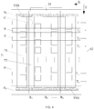
- the "first touch signal” is a driving signal or a sensing signal. If the first touch signal is a driving signal, the second electrode strips 72 are used as driving lines T (e.g., T1, T2...Tn in FIG. 5 ) in the touch structure. If the first touch signal is a sensing signal, the second electrode strips 72 are used as sensing lines R (e.g., R1, R2...Rn in FIG. 4 ) in the touch structure.
- the "first level signal terminal” refers to a node, a port or a wire at which corresponding first electrode strip(s) 71 is connected to a component configured to provide a first level signal (e.g., the VSS signal).
- the "first touch signal terminal” refers to a node, a port or a wire at which the second electrode strips 72 is connected to a component configured to provide or read the first touch signal.
- the first level signal terminal includes first level signal line(s).
- the touch display panel 200 further includes first level signal lines (hereinafter referred to as VSS signal lines) disposed at least at edge areas at both sides of the touch area A (e.g., areas A1 and A2) in the array substrate 1.
- VSS signal lines are perpendicular to the first electrode strips 71, and both ends of the first electrode strips 71 are respectively electrically connected to the VSS signal lines at corresponding sides.
- a plurality of VSS signal lines are connected into a frame structure. That is, the plurality of VSS signal lines are arranged in an enclosed manner in edge areas of the touch area A in the array substrate 1. In this way, the VSS signal lines respectively disposed in areas A1 and A2 in FIG. 4 may be electrically connected to each other, and structures and wires provided for transmitting VSS signals to the VSS signal lines may be saved.
- the VSS signal lines are disposed in the array substrate 1, for example, in a source-drain metal layer in the array substrate 1.
- the VSS signal lines are formed simultaneously with sources and drains of TFTs in the TFT array.
- the VSS signal lines are disposed in the pixel electrode layer in the array substrate 1.
- the VSS signal lines may be formed simultaneously with the pixel electrodes in the pixel electrode layer. In this way, a manufacturing process of the touch display panel 200 may be simplified.
- the first electrode strips 71 and the VSS signal lines are not disposed in a same layer, the first electrode strips 71 and the VSS signal lines are electrically connected through via holes.
- both ends of each second electrode strip 72 are separated and electrically insulated from the VSS signal lines by the insulating film layers.
- first level signal terminal described in some embodiments of the present disclosure is usually a low level signal terminal.
- first level signal line is usually a low level signal line, and the “first level signal” is usually a low level signal.
- each of the plurality of first electrode strips 71 is connected to a first level signal terminal (e.g., a VSS signal terminal) and a first touch signal terminal S1, and any two of the plurality of first electrode strips 71 are insulated from each other.
- the first electrode strips 71 may be reused in a time-share manner. For example, a time of a single frame is divided into a display period t1 and a touch period t2.
- the first level signal is transmitted to each first electrode strip 71 through the first level signal terminal (e.g., the VSS signal terminal), and each first electrode strip 71 is used as an electrode of the light-emitting device in the corresponding sub-pixel region, so as to ensure that the touch display panel 200 has the display function.
- the first touch signal is transmitted to each first electrode strip 71 through the first touch signal terminal S1, or first touch signals are read from the first electrode strips 71 through the first touch signal terminal S1, so as to achieve transmission of the first touch signal between each first electrode strip 71 and the first touch signal terminal S1. Since the first electrode strips are insulated from each other, the first touch signals transmitted by different first electrode strips 71 do not interfere with each other. Thereby, it may be ensured that the touch display panel 200 has the touch function.
- the second electrode strips 72 may be not used, and the display function and the touch function of the touch display panel 200 are realized by reusing the first electrode strips 71 in a time-share manner. Therefore, in a case where the directions in which the first electrode strips 71 and the second electrode strips 72 extend are regarded as length directions thereof, a design in which a width of the first electrode strips 71 is greater than a width of the second electrode strips 72 is adopted.
- the width of the first electrode strips 71 is set as wide as possible (the width is not limited by an area of the light-emitting layer 3 in the corresponding sub-pixel region).
- the width of the second electrode strips 72 is set as narrow as possible.
- insulating film layer(s) is disposed between the first electrode strips 71 and the first level signal terminal (e.g., the VSS signal terminal).
- the first electrode strips 71 are connected to the first level signal terminal (e.g., the VSS signal terminal) through corresponding via holes disposed in the insulating film layer(s). Therefore, under a premise of ensuring mutual insulation among the first electrode strips 71, the first level signal supplied by the first level signal terminal (e.g., the VSS signal terminal) are transmitted to the first electrode strips 71.
- the first level signal terminal e.g., the VSS signal terminal
- a shape of the touch area A of the touch display panel 200 is set to be rectangular.
- the first electrode strips 71 and the second electrode strips 72 extend along a length direction Y of the touch area A. That is, the first electrode strips 71 and the second electrode strips 72 are parallel to a long side of the touch area A, as shown in FIG. 4 .
- the first electrode strips 71 and second electrode strips 72 extend along a width direction X of the touch area A. That is, the first electrode strips 71 and the second electrode strips 72 are parallel to a wide side of the touch area A, as shown in FIG. 5 .
- the design in which the first electrode strips 71 extend along the width direction X of the touch area A allows for a shorter length of the first electrodes 71. In this way, the electric resistance on each first electrode strip 71 may be further reduced, and thus the voltage drop on the first electrode strips 71 may be further reduced.
- the touch display panel 200 further includes: a TFE layer 5 disposed on a side of the divided electrode layer 7 away from the array substrate 1; and a touch electrode layer disposed on a side of the TFE layer 5 away from the array substrate 1.
- the touch electrode layer includes a plurality of third electrode strips 9 disposed across the plurality of first electrode strips 71 or the plurality of second electrode strips 72.
- the third electrode strips 9 are connected to a second touch signal terminal S2 to transmit second touch signal(s), and any two of the third electrode strips 9 are insulated from each other.
- the plurality of third electrode strips 9 are perpendicular to the plurality of first electrode strips 71.
- the plurality of third electrode strips 9 are perpendicular to the plurality of second electrode strips 72.
- the TFE layer 5 can protect organic light-emitting materials of the light-emitting layers 3 from being damaged by water vapor in the external environment; on another hand, the TFE layer 5 can be used as an insulating layer between the plurality of third electrode strips 9 and both the plurality of first electrode strips 71 and the plurality of second electrode strips 72.
- the first touch signal is a driving signal for realizing a touch function
- the second touch signal is a sensing signal generated by sensing a touch position
- the first electrode strips 71 are used as driving lines T of the touch structure
- the third electrode strips 9 are used as sensing lines R of the touch structure.
- the first electrode strips 71 are used as sensing lines R of the touch structure
- the third electrode strips 9 are used as driving lines T of the touch structure.
- each third electrode strip 9 is disposed in a gap region between two corresponding adjacent lines of pixel electrodes 8.
- an orthographic projection of each third electrode strip 9 at least partially overlaps with a gap region between orthographic projections of adjacent two lines of pixel electrodes 8, and there is a small overlap (of course, there may be no overlap) between edges of the orthographic projection of each third electrode strip 9 along a direction in which the third electrode strips 9 extend and orthographic projections of two lines of pixel electrodes 8 located on both sides of the third electrode strip 9.
- a parasitic capacitance between the third electrode strips 9 and adjacent pixel electrodes 8 may be reduced, and an influence of the third electrode strips 9 on a light transmittance of the sub-pixel regions in which the third electrode strips 9 are located may be reduced.
- the plurality of electrode dividing strips 6 divide the divided electrode layer 7 into a plurality of first electrode strips 71 and a plurality of second electrode strips 72, such that the first electrode strips 71 are located on the surfaces of the light-emitting layers 3 away from the array substrate 1, and the second electrode strips 72 are located on surfaces of the electrode dividing strips 6 away from the array substrate 1.
- each first electrode strip 71 is used as an electrode (a cathode or an anode) of the light-emitting device in a corresponding sub-pixel region
- each second electrode strip 72 is used as a signal line (a driving line T or a sensing line R) in the touch structure.
- the touch structure may be integrated into a display panel to obtain the touch display panel 200.
- the touch structure may be integrated into the display panel to obtain the touch display panel 200 by reusing the first electrode strips 71 in a time-share manner, that is, using each first electrode strip 71 as an electrode of the light-emitting device in the corresponding sub-pixel region during the display period t1, and as a signal line of the touch structure during the touch period t2.
- the structure provided in some embodiments of the present disclosure is much simpler because an electrode of the light-emitting device and a signal line of the touch structure are in a same layer (e.g., the divided electrode layer 7).
- the divided electrode layer 7 is located at an inner side of the TFE layer 5 (i.e., a side of the TFE layer 5 proximate to the array substrate 1). That is, in some embodiments of the present disclosure, at least a part of the touch structure is integrated inside the display panel. Therefore, the touch display panel 200 obtained by adopting such a structure is thinner and lighter.
- the structure provided in some embodiments of the present disclosure may be able to effectively reduce an electrical resistance on a corresponding electrode in the light-emitting device and thus reduce a voltage drop on the corresponding electrode in the light-emitting device because the strip-shaped plurality of first electrode strips 71 are used as electrodes of light-emitting devices in corresponding sub-pixel regions.
- Some embodiments of the present disclosure further provide a method of manufacturing a touch display panel.
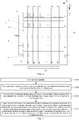
- the method includes step 100 to step 400 (S100 to S400).
- an array substrate is formed.
- the above step of forming the array substrate includes: forming a TFT array on a base substrate, and forming a plurality of pixel electrodes on a side of the TFT array away from the base substrate.
- the pixel electrodes are respectively connected to corresponding driving TFTs in the TFT array.
- a pixel defining layer is formed on a side of the array substrate, and light-emitting layers are formed in sub-pixel regions defined by the pixel defining layer.
- a patterned pixel defining layer 2 is formed on a side of the formed array substrate 1.
- the pixel defining layer 2 has a plurality of sub-pixel patterns that look like openings, so as to define a plurality of sub-pixel regions in the touch display panel.
- light-emitting layers 3 are formed in openings of the sub-pixel regions defined by the pixel defining layer 2.
- a material of the light-emitting layer 3 is an organic light-emitting material.
- Light-emitting layers 3 capable of emitting different colors of light are formed in different sub-pixel regions.
- a plurality of electrode dividing strips are formed on a side of the pixel defining layer away from the array substrate, and the plurality of electrode dividing strips divide a touch area into a plurality of strip-shaped areas.
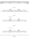
- the step of forming a plurality of electrode dividing strips 6 on the side of the pixel defining layer 2 away from the array substrate 1 includes step 301 and step 302 (S301 and S302).
- a photoresist layer 6' is formed by a coating process on a side of the pixel defining layer 2 away from the array substrate 1.
- the photoresist layer 6' is exposed, developed and etched to remove photoresist materials in regions of the photoresist layer 6' other than regions where the electrode dividing strips are located.
- the plurality of electrode dividing strips 6 are formed by remaining photoresist materials on the pixel defining layer 2.
- regions that need to be exposed and developed in a case where the photoresist layer 6' is formed by a positive photoresist material are different from those in a case where the photoresist layer 6' is formed by a negative photoresist material.
- the regions that need to be exposed and developed are the regions of the photoresist layer 6' other than regions where the electrode dividing strips are located.
- the regions that need to be exposed and developed are the regions where the electrode dividing strips are located.
- FIGS. 9 and 10 show an example in which the photoresist layer 6' is formed of a positive photoresist material.
- an electrode material is deposited on a side of the plurality of electrode dividing strips away from the array substrate to form a divided electrode layer.
- the divided electrode layer is divided by the plurality of electrode dividing strips to form a plurality of first electrode strips located in the plurality of strip-shaped areas and a plurality of second electrode strips located on surfaces of the plurality of electrode dividing strips away from the array substrate, and the plurality of second electrode strips are insulated from the plurality of first electrode strips.
- the electrode material in a process of depositing the electrode material on the side of the plurality of electrode dividing strips 6 away from the array substrate 1, a part of the electrode material falls on the surfaces of the light-emitting layers 3 away from the array substrate 1 to form a plurality of first electrode strips 71. Another part of the electrode material falls on the surfaces of the plurality of electrode dividing strips 6 away from the array substrate 1 to form a plurality of second electrode strips 72. Due to existence of the electrode dividing strips 6, the plurality of first electrode strips 71 may be insulated from the plurality of second electrode strips 72. That is to say, the divided electrode layer 7 is divided into a plurality of first electrode strips 71 and a plurality of second electrode strips 72 by the plurality of electrode dividing strips 6.
- the plurality of first electrode strips 71 are correspondingly located in the plurality of strip-shaped areas formed after the touch area is divided by the plurality of electrode dividing strips 6, and are located on the surfaces of the light-emitting layers 3 away from the array substrate 1.
- the plurality of second electrode strips 72 are correspondingly located on the surfaces of the plurality of electrode dividing strips 6 away from the array substrate 1.
- the method of manufacturing the touch display panel further includes step 500 and step 600 (S500 and S600).
- a TFE layer is formed on a side of the divided electrode layer away from the array substrate.
- the TFE layer 5 is formed on the side of the divided electrode layer 7 away from the array substrate 1. In this way, the TFE layer 5 may be used to protect the divided electrode layer 7 and light-emitting materials in the light-emitting layers 3.
- a touch electrode layer is formed on a side of the TFE layer away from the array substrate.
- the touch electrode layer includes a plurality of third electrode strips disposed across the plurality of first electrode strips or the plurality of second electrode strips, and any two of the plurality of third electrode strips are insulated from each other.
- the plurality of first electrode strips 71 are disposed in parallel with the plurality of second electrode strips 72.
- a plurality of third electrode strips 9 are formed on a side of the TFE layer 5 away from the array substrate 1, such that directions in which the plurality of third electrode strips 9 extend are perpendicular to the directions in which the plurality of first electrode strips 71 extend, and the directions in which the plurality of third electrode strips 9 extend are perpendicular to the directions in which the plurality of second electrode strips 72 extend.
- the plurality of first electrode strips 71 and the plurality of second electrode strips 72 are simultaneously formed by a film layer deposition process, which greatly simplifies the manufacturing process of the touch display panel.
- Some embodiments of the present disclosure further provide a method of driving a touch display panel, which is applied to a touch display panel provided in some embodiments of the present disclosure.
- a time of a single frame is a driving period t, and the method of driving the touch display panel includes one of the following two solutions.
- Solution 1 Referring to FIGS. 4 and 5 , in a touch display panel that adopts Solution 1, at least one of the plurality of first electrode strips 71 is connected to a first level signal terminal (e.g., a VSS signal terminal), and any adjacent two of the first electrode strips 71 are shorted to each other.
- a first level signal terminal e.g., a VSS signal terminal
- any adjacent two of the first electrode strips 71 are shorted to each other.
- Each of the plurality of second electrode strips 72 is connected to a first touch signal terminal S1
- any two of the plurality of second electrode strips 72 are insulated from each other.
- a first level signal e.g., a VSS signal
- the plurality of second electrode strips 72 transmit first touch signal(s) respectively.
- each pixel electrode 8 in the touch display panel is used as an anode of the light-emitting device in a corresponding sub-pixel region.
- the cathode and the anode together drive the light-emitting layer 3 in the light-emitting device to emit light, thereby realizing the display function of the touch display panel.
- the second touch signal read and obtained from the third electrode strips 9 in the touch display panel is a sensing signal generated by sensing the touch position.
- a second touch signal that need to be applied to the third electrode strips 9 in the touch display panel is a driving signal for realizing the touch function.
- a mutual capacitance C may be formed at each intersection of the second electrode strips 72 and the third electrode strips 9, which enables the touch display panel to have the touch function.
- Solution 2 Referring to FIG. 6 , in a touch display panel that adopts Solution 2, the plurality of first electrode strips 71 are connected to a first level signal terminal (e.g., a VSS signal terminal) and a first touch signal terminal S1, and any two of the plurality of first electrode strips 71 are shorted to each other.
- a first level signal e.g., a VSS signal
- a first level signal is applied to the plurality of first electrode strips 71 in the display period t1.
- the plurality of first electrode strips 71 transmit first touch signal(s) in the touch period t2.
- a Vertical Driving (VD) signal is able to control the touch display panel 20 to enter the touch period t2 or the display period t1.
- VD Vertical Driving
- the touch period t2 is usually set in a vertical blanking period of each frame.
- the touch period t2 is set in the vertical blanking period, and durations of the touch period t2 and the vertical blanking period are the same.
- a duration of the vertical blanking period in a time of each frame is equal to a length of a time interval in which a scanning signal returns from a lower right corner of a screen to an upper left corner of the screen after scanning of a current frame is completed and before scanning of a next frame begins. Since the touch period t2 is set in the vertical blanking period, normal display of the touch display panel will not be affected.
- the VD signal is set high, and a Vertical Sync (VSYNC, abbreviated as VS in FIG. 16 ) signal and a Horizontal Sync (HSYNC, abbreviated as HS in FIG. 16 ) signal are both set low, so as to drive the touch display panel.
- the VD signal is set low, the VSYNC signal is set high, and the HSYNC signal includes a plurality of high level pulses that are sequentially output in a horizontal timing cycle, so as to drive the touch display panel.
- each pixel electrode 8 in the touch display panel is used as an anode of the light-emitting device in a corresponding sub-pixel region.
- the cathode and the anode together drive the light-emitting layer 3 in the light-emitting device to emit light, thereby realizing the display function of the touch display panel in the display period t1.
- the second touch signal read and obtained from the third electrode strips 9 in the touch display panel is a sensing signal generated by sensing the touch position.
- the second touch signal that need to be applied to the third electrode strips 9 in the touch display panel is a driving signal for realizing the touch function.
- a mutual capacitance C may be formed at each intersection of the first electrode strips 71 and the third electrode strips 9, which enables the touch display panel to have the touch function in the touch period t2.
- the display function and the touch function of the touch display panel 200 may be realized by reusing the first electrode strips 71 in a time-share manner without using the second electrode strips 72. Therefore, in a case where the directions in which the first electrode strips 71 and the second electrode strips 72 extend are regarded as the length directions thereof, the design in which the width of the first electrode strips 71 is greater than the width of the second electrode strips 72 is adopted.
- the width of the first electrode strips 71 may not be limited by the area of the light-emitting layer 3 in the corresponding sub-pixel region, and the width of the first electrode strip 71 may be set as wide as possible. In this way, the electric resistance on each first electrode strip 71 may be further reduced, and a signal-to-noise ratio of sensing signals obtained through the first electrode strips 71 may be improved.
- the touch display device 1001 includes a touch display panel 200 provided in some embodiments of the present disclosure.
- the touch display device has the advantages of a simple overall structure, light weight, and simple manufacturing process.
- the touch display device provided in some embodiments of the present disclosure is any product or component having a display function, such as an OLED panel, a mobile phone, a tablet computer, a television, a monitor, a notebook computer, a digital photo frame, or a navigator.
- a display function such as an OLED panel, a mobile phone, a tablet computer, a television, a monitor, a notebook computer, a digital photo frame, or a navigator.
Landscapes
- Engineering & Computer Science (AREA)
- Theoretical Computer Science (AREA)
- General Engineering & Computer Science (AREA)
- Physics & Mathematics (AREA)
- General Physics & Mathematics (AREA)
- Human Computer Interaction (AREA)
- Microelectronics & Electronic Packaging (AREA)
- Optics & Photonics (AREA)
- Manufacturing & Machinery (AREA)
- Electroluminescent Light Sources (AREA)
- Devices For Indicating Variable Information By Combining Individual Elements (AREA)
Abstract
Description
- The present application claims priority to Chinese Patent Application No.
201810515682.8 - The present disclosure relates to the field of display technologies, and in particular, to a touch display panel, a method of manufacturing the same, a method of driving the same, and a touch display device.
- Organic light-emitting diode (OLED) display devices have attracted more and more attention and are increasingly favored by the display industry due to their advantages of self-luminescence, high contrast, high color gamut, wide viewing angle, light and thin structure, and compatibility with flexible substrates, and are referred to as one of the next-generation display technologies. Moreover, with the continuous development of display technologies, touch structures are increasingly being integrated into the OLED display devices.
- In an aspect, a touch display panel is provided. The touch display panel includes: an array substrate; a pixel defining layer disposed on a side of the array substrate, light-emitting layers being disposed in sub-pixel regions defined by the pixel defining layer; a plurality of electrode dividing strips disposed on a side of the pixel defining layer away from the array substrate, the plurality of electrode dividing strips dividing a touch area into a plurality of strip-shaped areas; and a divided electrode layer disposed on a side of the plurality of electrode dividing strips away from the array substrate.
- The divided electrode layer includes: a plurality of first electrode strips located in the plurality of strip-shaped areas; and a plurality of second electrode strips located on surfaces of the plurality of electrode dividing strips away from the array substrate, the plurality of second electrode strips being insulated from the plurality of first electrode strips.
- In some embodiments of the present disclosure, at least one of the plurality of first electrode strips is connected to a first level signal terminal, and any adjacent two of the first electrode strips are shorted to each other; each of the plurality of second electrode strips is connected to a first touch signal terminal, and any two of the plurality of second electrode strips are insulated from each other.
- In some embodiments of the present disclosure, the first level signal terminal includes first level signal line(s). The touch display panel further includes first level signal lines disposed at least at edge areas at both sides of the touch area. The first level signal lines are perpendicular to the plurality of first electrode strips, and both ends of the plurality of first electrode strips are respectively electrically connected to the first level signal lines at corresponding sides.
- In some embodiments of the present disclosure, each of the plurality of first electrode strips is connected to a first level signal terminal and a first touch signal terminal, and any two of the plurality of first electrode strips are insulated from each other.
- In some embodiments of the present disclosure, a shape of the touch area includes a rectangle. The plurality of first electrode strips extend along a length direction of the touch area. Or, the plurality of first electrode strips extend along a width direction of the touch area.
- In some embodiments of the present disclosure, a material of the electrode dividing strip includes a positive photoresist. A shape of a cross section of the electrode dividing strip perpendicular to a direction in which the electrode strip extends is a trapezoid. A length of a side of the trapezoid away from the array substrate is less than a length of a side of the trapezoid proximate to the array substrate. Or, a material of the electrode dividing strip includes a negative photoresist. A shape of the cross section of the electrode dividing strip perpendicular to a direction in which the electrode strip extends is an inverted trapezoid. A length of a side of the inverted trapezoid away from the array substrate is greater than a length of a side of the inverted trapezoid proximate to the array substrate.
- In some embodiments of the present disclosure, directions in which the plurality of electrode dividing strips extend are parallel to a column direction of the sub-pixel regions defined by the pixel defining layer, and at least one column of the sub-pixel regions is disposed between any adjacent two electrode dividing strips. Or, directions in which the plurality of electrode dividing strips extend are parallel to a row direction of the sub-pixel regions defined by the pixel defining layer, and at least one row of the sub-pixel regions is disposed between any adjacent two electrode dividing strips.
- In some embodiments of the present disclosure, at least one of the plurality of first electrode strips is located on a surface of a light-emitting layer away from the array substrate in a corresponding sub-pixel region. In some embodiments of the present disclosure, a thickness of the electrode dividing strip in a direction perpendicular to the array substrate is 1 µm to 2 µm, and a thickness of the divided electrode layer in a direction perpendicular to the array substrate is 10 nm to 20nm.
- In some embodiments of the present disclosure, the touch display panel further includes: a thin film encapsulation (TFE) layer disposed on a side of the divided electrode layer away from the array substrate; and a touch electrode layer disposed on a side of the TFE layer away from the array substrate. The touch electrode layer includes a plurality of third electrode strips disposed across the plurality of first electrode strips or the plurality of second electrode strips, the plurality of third electrode strips are respectively connected to a second touch signal terminal, and any two of the plurality of third electrode strips are insulated from each other.
- In some embodiments of the present disclosure, the plurality of third electrode strips are perpendicular to the plurality of first electrode strips or the plurality of second electrode strips.
- In another aspect, a method of manufacturing a touch display panel is provided. The method includes:
- forming an array substrate;
- forming a pixel defining layer on a side of the array substrate, and forming light-emitting layers in sub-pixel regions defined by the pixel defining layer;
- forming a plurality of electrode dividing strips on a side of the pixel defining layer away from the array substrate, the plurality of electrode dividing strips dividing a touch area into a plurality of strip-shaped areas; and
- depositing an electrode material on a side of the plurality of electrode dividing strips away from the array substrate to form a divided electrode layer.
- In a process of depositing the electrode material, the divided electrode layer is divided by the plurality of electrode dividing strips to form a plurality of first electrode strips located in the plurality of strip-shaped areas and a plurality of second electrode strips located on surfaces of the plurality of electrode dividing strips away from the array substrate, and the plurality of second electrode strips are insulated from the plurality of first electrode strips.
- In some embodiments of the present disclosure, the method of manufacturing the touch display panel further includes:
- forming a TFE layer on a side of the divided electrode layer away from the array substrate; and
- forming a touch electrode layer on a side of the TFE layer away from the array substrate, the touch electrode layer including a plurality of third electrode strips disposed across the plurality of first electrode strips or the plurality of second electrode strips, and any two of the plurality of third electrode strips being insulated from each other.
- In yet another aspect, a method of driving a touch display panel is provided. The method includes: applying a first level signal to a plurality of first electrode strips in a time of a single frame, and making a plurality of second electrode strips transmit first touch signals respectively.
- In yet another aspect, a method of driving a touch display panel is provided. The method includes: dividing a time of a single frame into a display period and a touch period; applying a first level signal to a plurality of first electrode strips in the display period; and making a plurality of first electrode strips transmit first touch signals respectively in the touch period.
- In yet another aspect, a touch display device is provided. The touch display device includes the touch display panel as described above.
- In order to describe technical solutions in some embodiments of the present disclosure more clearly, the accompanying drawings to be used in the description of disclosure will be introduced briefly. Obviously, the accompanying drawings to be described below are merely some embodiments of the present disclosure, and a person of ordinary skill in the art can obtain other drawings according to these drawings without paying any creative effort.
-
FIG. 1 is a schematic structural diagram of a conventional OLED display panel according to the related art; -
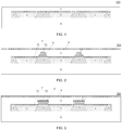
FIG. 2 is a schematic cross-sectional view of a touch display panel according to some embodiments of the present disclosure; -
FIG. 3 is a schematic cross-sectional view of another touch display panel according to some embodiments of the present disclosure; -
FIG. 4 is a schematic plan view of a touch display panel according to some embodiments of the present disclosure; -
FIG. 5 is a schematic plan view of another touch display panel according to some embodiments of the present disclosure; -
FIG. 6 is a schematic plan view of yet another touch display panel according to some embodiments of the present disclosure; -
FIG. 7 is a flow chart of a method of manufacturing a touch display panel according to some embodiments of the present disclosure; -
FIG. 8 is a flow chart of another method of manufacturing a touch display panel according to some embodiments of the present disclosure; -
FIGS. 9 to 15 are schematic diagrams showing steps of the method of manufacturing the touch display panel shown inFIG. 8 ; -
FIG. 16 is a timing control diagram of a method of driving a touch display panel according to some embodiments of the present disclosure; and -
FIG. 17 is a schematic structural diagram of a touch display device according to some embodiments of the present disclosure. - There are mainly three touch structures that can be integrated into an OLED display device, as described below:
- 1) add on mode structure: touch sensing modules are attached to an OLED display panel;
- 2) multi-layer on cell (MLOC) structure: a MLOC touch structure is directly formed on a thin film encapsulation (TFE) layer of an OLED display panel; and
- 3) block electrode structure: a cathode layer of an OLED display panel is patterned to form a plurality of block electrodes, which are reused to realize a cathode function and a touch sensing function.
- The above structures 1) and 2) have disadvantages of a complex structure, a thick display panel, and a high manufacturing cost. Although the structure 3) has advantages of a simple structure, a light and thin display panel, and a low manufacturing cost, after the cathode layer is patterned to form block electrodes, a resistance at cathodes will be significantly increased. Consequently, a voltage drop at the cathodes will increase dramatically, resulting in higher power consumption of the display panel.
- Based on this, the technical solutions in embodiments of the present disclosure will be described clearly and completely with reference to the accompanying drawings in the embodiments of the present disclosure. Obviously, the described embodiments are merely some but not all of the embodiments of the present disclosure. All other embodiments obtained on the basis of some embodiments of the present disclosure by a person of ordinary skill in the art without paying any creative effort shall be included in the protection scope of the present disclosure.
- In some embodiments of the present disclosure, an OLED display panel is used as an application scenario. A structure of a conventional OLED display panel is briefly introduced below. It will be noted that, application scenarios on which some embodiments of the present disclosure are based are merely examples, and those skilled in the art have the ability to apply inventive concepts of some embodiments of the present disclosure to other scenarios.
- As shown in
FIG. 1 , the conventionalOLED display panel 100 mainly includes: anarray substrate 1, apixel defining layer 2, light-emittinglayers 3, a cathode layer 4, and a thin film encapsulation (TFE)layer 5. Thearray substrate 1 includes: a base substrate, a thin film transistor (TFT) array disposed on the base substrate, and a plurality of pixel electrodes disposed on a side of the TFT array away from the base substrate. The plurality of pixel electrodes are connected to driving TFTs of sub-pixels in one-to-one correspondence. Thepixel defining layer 2 is configured to define sub-pixel regions of the OLED display panel. The light-emittinglayers 3 are located in the sub-pixel regions defined by thepixel defining layer 2. The cathode layer 4 covers surfaces of thepixel defining layer 2 and the light-emittinglayers 3 away from thearray substrate 1. A pixel electrode, a light-emittinglayer 3, and the cathode layer 4 in a sub-pixel region together constitute a light-emitting device. TheTFE layer 5 covers a surface of the cathode layer 4 facing away from thearray substrate 1, and serves to encapsulate all light-emitting devices. - Referring to
FIGS. 2 and 3 , some embodiments of the present disclosure provide atouch display panel 200, which realizes integration of a touch structure into thedisplay panel 100. Thetouch display panel 200 includes anarray substrate 1, and apixel defining layer 2 disposed on a side of thearray substrate 1. Light-emittinglayers 3 are disposed in sub-pixel regions defined by thepixel defining layer 2. Thetouch display panel 200 further includes: a plurality of electrode dividing strips 6 disposed on a side of thepixel defining layer 2 away from thearray substrate 1, and a dividedelectrode layer 7 disposed on a side of the plurality of electrode dividing strips 6 away from thearray substrate 1. - Referring to
FIGS. 2 to 6 , the plurality of electrode dividing strips 6 divide a touch area into a plurality of strip-shaped areas. The dividedelectrode layer 7 includes: a plurality of first electrode strips 71 located in the plurality of strip-shaped areas, and a plurality of second electrode strips 72 located on surfaces of the plurality of electrode dividing strips 6 away from thearray substrate 1. The plurality of first electrode strips 71 are insulated from the plurality of second electrode strips 72. - The touch area of the
touch display panel 200 is also a display area, and the touch area includes the sub-pixel regions defined by thepixel defining layer 2. Thereby, at least some of the strip-shaped areas defined by the plurality of electrode dividing strips 6 are provided with light-emittinglayers 3, and surfaces of the light-emittinglayers 3 away from thearray substrate 1 are covered by at least some of the first electrode strips 71 of the dividedelectrode layer 7. That is to say, at least one of the plurality of first electrode strips 71 of the dividedelectrode layer 7 is located on a surface of a light-emittinglayer 3 away from thebase substrate 1 in a corresponding sub-pixel region, so that it may be used as an electrode of a light-emitting device that includes the light-emittinglayer 3. Referring toFIGS. 2 to 6 , the plurality of electrode dividing strips 6 are disposed on the side of thepixel defining layer 2 away from thearray substrate 1. That is, one electrode dividing strips 6 is disposed in a gap region between two lines (i.e., two rows or two columns) of sub-pixel regions. In this way, the electrode dividing strips 6 are prevented from blocking light emitted by corresponding sub-pixel regions. - For example, the plurality of electrode dividing strips 6 are parallel or substantially parallel to each other, and any adjacent two electrode dividing strips 6 are separated by a certain region, so that there is a strip-shaped area between any adjacent two electrode dividing strips 6. The region between any adjacent two electrode dividing strips 6 is at least one line (one row or one column) of sub-pixel regions. Further, areas of regions between any adjacent two electrode dividing strips 6 are the same. In this way, the subsequently formed plurality of first electrode strips 71 and plurality of second electrode strips 72 are distributed evenly, which is conducive to improving performances of the touch display panel.
- In addition, directions in which the plurality of electrode dividing strips 6 extend may be parallel to a column direction of the sub-pixel regions, or parallel to a row direction of the sub-pixel regions, which is determined according to design requirements of the subsequently formed plurality of first electrode strips 71 and plurality of second electrode strips 72. If the electrode dividing strips 6 are parallel to the column direction of the sub-pixel regions, then at least one column of sub-pixel regions is disposed between any adjacent two electrode dividing strips 6. If the electrode dividing strips 6 are parallel to the row direction of the sub-pixel regions, then at least one row of sub-pixel regions is disposed between any adjacent two electrode dividing strips 6.
- In a case where a single column (or a single row) of sub-pixel regions is disposed between any adjacent two electrode dividing strips 6, each column (or each row) of sub-pixel regions correspond to a single
first electrode strip 71 and a singlesecond electrode strip 72. Thus, there will be a large number of first electrode strips 71 and second electrode strips 72, and in turn a large number of touch points. As a result, a touch accuracy of thetouch display panel 200 may be improved. - In a case where multiple columns (or multiple rows) of sub-pixel regions are disposed between any adjacent two electrode dividing strips 6, the multiple columns (or multiple rows) of sub-pixel regions correspond to a single
first electrode strip 71 and a singlesecond electrode strip 72. That is, the dividedelectrode layer 7 is divided into a smaller number of first electrode strips 71 and second electrode strips 72, which means that the number of first electrode strips 71 is small. However, in this case, eachfirst electrode strip 71 occupies a large area, which is conducive for reducing an electric resistance of thefirst electrode strip 71 in a case where the first electrode strip 71 (covering a light-emittinglayer 3 in a corresponding sub-pixel region) is used as an electrode of a light-emitting device. Therefore, a voltage drop at thefirst electrode strip 71 being used as the electrode of the light-emitting device may be reduced. - It will be understood that, a material forming the
electrode dividing strip 6 is an insulating material. In this way, it may be possible to ensure electrical insulation between the first electrode strips 71 and the second electrode strips 72 that are subsequently formed. Optionally, the material forming theelectrode dividing strip 6 is a photoresist. By forming a photoresist layer on the surfaces of thepixel defining layer 2 and the light-emittinglayers 3 away from thearray substrate 1 through a coating process, and by exposing and developing specific areas of the photoresist layer, the required electrode dividing strips 6 may be formed. - Based on this, further, as a type of photoresist used to form the electrode dividing strips 6 differs, shapes of the formed electrode dividing strips 6 are also different. For example, the material forming the
electrode dividing strip 6 is a positive photoresist. Since the positive photoresist will be changed from an insoluble photoresist to a soluble photoresist after an exposure process, regions of the photoresist layer other than regions where the electrode dividing strips are located is exposed in a process of forming the electrode dividing strips 6. Therefore, a shape of a cross section of the finally formedelectrode dividing strip 6 perpendicular to thearray substrate 1 and perpendicular to a direction in which theelectrode dividing strip 6 extends is a trapezoid, as shown inFIG. 2 . In contrast, the material forming theelectrode dividing strip 6 is a negative photoresist. Since the positive photoresist will be changed from a soluble photoresist to an insoluble photoresist after the exposure process, the regions where the electrode dividing strips are located is exposed in a process of forming the electrode dividing strips 6. Therefore, the shape of the cross section of the finally formedelectrode dividing strip 6 perpendicular to thearray substrate 1 and perpendicular to the direction in which theelectrode dividing strip 6 extends is an inverted trapezoid, as shown inFIG. 3 . - It will be noted that, the term "trapezoid" means that: of two sides of the trapezoid that are parallel to the
array substrate 1, a length of a side away from thearray substrate 1 is less than a length of a side proximate to thearray substrate 1. In contrast, the term "inverted trapezoid" means that: of two sides of the inverted trapezoid that are parallel to thearray substrate 1, a length of a side away from thearray substrate 1 is greater than a length of a side proximate to thearray substrate 1. - It will be noted that, in a case where the shape of the cross section of the
electrode dividing strip 6 is an inverted trapezoid, each side wall and a bottom surface (i.e., a side in contact with the pixel defining layer 6) of theelectrode dividing strip 6 form an obtuse angle. Therefore, in a subsequent process of depositing the dividedelectrode layer 7 to form the first electrode strips 71 and the second electrode strips 72 at a same time, the first electrode strips 71 and the second electrode strips 72 may more easily disconnected, as compared with a case where the shape of the cross section of theelectrode dividing strip 6 is a trapezoid. In other words, it may be easier to cut the dividedelectrode layer 7 clearly with less cutting residues. - In addition, by designing a thickness of the electrode dividing strip 6 (i.e., a size of the
electrode dividing strip 6 in a direction perpendicular to the array substrate 1) and a thickness of the dividedelectrode layer 7 in a certain way respectively, it may also be possible to ensure that the first electrode strips 71 and the second electrode strips 72 are easily disconnected and electrode material residues between the two are reduced in the subsequent process of depositing the dividedelectrode layer 7 to form the first electrode strips 71 and the second electrode strips 72 at the same time. For example, the thickness of theelectrode dividing strip 6 may be increased as much as possible under a premise of not significantly increasing an overall thickness of thetouch display panel 200. Moreover, the thickness of the dividedelectrode layer 7 may be reduced as much as possible on a basis of ensuring that the first electrode strips 71 and the second electrode strips 72 have good electrical conductivity. Thus, in the process of depositing the dividedelectrode layer 7 on surfaces of the electrode dividing strips 6, the first electrode strips 71 and the second electrode strips 72 may be easily separated from each other. - Optionally, a thickness of the
electrode dividing strip 6 is 1 µm to 2 µm, and a thickness of the dividedelectrode layer 7 is 10 nm to 20 nm. Since thicknesses of theelectrode dividing strip 6 and the dividedelectrode layer 7 are not in a same order of magnitude, the dividedelectrode layer 7 may be more easily divided when the dividedelectrode layer 7 is being deposited on the electrode dividing strips 6 to form the first electrode strips 71 and the second electrode strips 72. - Referring to
FIGS. 2 and 3 , in some embodiments of the present disclosure, the plurality of first electrode strips 71 included in thetouch display panel 200 are correspondingly located in the plurality of strip-shaped areas formed after the touch area is divided by the plurality of electrode dividing strips 6, and on surfaces of the light-emittinglayers 3 away from thearray substrate 1. The plurality of second electrode strips 72 included in thetouch display panel 200 are correspondingly located on the surfaces of the plurality of electrode dividing strips 6 away from thearray substrate 1. The first electrode strips 71 and the second electrode strips 72 are alternately arranged. Thus, in a process of depositing an electrode material on surfaces of the plurality of electrode dividing strips 6 and the light-emittinglayers 3 away from thearray substrate 1, a plurality of first electrode strips 71 and a plurality of second electrode strips 72 may be formed at the same time, and separated and insulated from each other. - The
touch display panel 200 has both a display function and a touch function. In some embodiments of the present disclosure, referring toFIGS. 4 and5 , at least one of the plurality of first electrode strips 71 is connected to a first level signal terminal (e.g., a common voltage signal terminal VSS), and any adjacent two of the first electrode strips 71 are shorted to each other. Thus, a potential of eachfirst electrode strip 71 is a potential supplied by the first level signal terminal. Eachfirst electrode strip 71 may be used as an electrode of a light-emitting device in a corresponding sub-pixel region, so as to ensure that the touch display panel has the display function. Moreover, referring toFIGS. 4 and5 , each of the plurality of second electrode strips 72 is connected to a first touch signal terminal S1, and any two of the plurality of second electrode strips 72 are insulated from each other. In this way, eachsecond electrode strip 72 may be able to transmit a first touch signal to the first touch signal terminal S1, and it may be ensured that first touch signals transmitted by different second electrode strips 72 do not interfere with each other, such that thetouch display panel 200 has the touch function. - Therefore, in a case where the above structure is adopted, the
touch display panel 200 provided in some embodiments of the present disclosure may be able to perform the display function and the touch function simultaneously, the two functions are independent of each other and do not interference with each other much, and thetouch display panel 200 has a good display effect and a high touch sensitivity. - It will be noted that, under normal circumstances, the
array substrate 1 includes pixel electrodes that correspond to respective sub-pixel regions, and the pixel electrodes are used as anodes of corresponding light-emitting devices. Each of the plurality of first electrode strips 71 covering the light-emittinglayers 3 is used as a cathode of a light-emitting device including a corresponding light-emittinglayer 3. In addition, since any adjacent two of the first electrode strips 71 are shorted to each other, so that the first electrode strips 71 are electrically connected to each other, even if only one or a few first electrode strips 71 are connected to the first level signal terminal (e.g., a VSS signal terminal), it may also be possible to make a potential of eachfirst electrode strip 71 equal to a potential supplied by the first level signal terminal (e.g., a common voltage VSS). Thus, in some embodiments of the present disclosure, one or a few first electrode strips 71 are connected to the first level signal terminal (e.g., the VSS signal terminal). In this way, a connection manner of the first electrode strips 71 and the first level signal terminal may be simplified. Of course, in some other embodiments of the present disclosure, a structure in which most or even all of the first electrode strips 71 are connected to the first level signal terminal (e.g., the VSS signal terminal) is adopted. This is also allowed. In this way, a loss of potential signal (e.g., VSS signal) supplied by the first level signal terminal during a transmission process may be reduced. - It will be noted that, in some embodiments of the present disclosure, the "first touch signal" is a driving signal or a sensing signal. If the first touch signal is a driving signal, the second electrode strips 72 are used as driving lines T (e.g., T1, T2...Tn in
FIG. 5 ) in the touch structure. If the first touch signal is a sensing signal, the second electrode strips 72 are used as sensing lines R (e.g., R1, R2...Rn inFIG. 4 ) in the touch structure. - In addition, in some embodiments of the present disclosure, the "first level signal terminal" refers to a node, a port or a wire at which corresponding first electrode strip(s) 71 is connected to a component configured to provide a first level signal (e.g., the VSS signal). Likewise, the "first touch signal terminal" refers to a node, a port or a wire at which the second electrode strips 72 is connected to a component configured to provide or read the first touch signal.
- Based on this, in some embodiments of the present disclosure, referring to
FIG. 4 , the first level signal terminal includes first level signal line(s). Thetouch display panel 200 further includes first level signal lines (hereinafter referred to as VSS signal lines) disposed at least at edge areas at both sides of the touch area A (e.g., areas A1 and A2) in thearray substrate 1. The VSS signal lines are perpendicular to the first electrode strips 71, and both ends of the first electrode strips 71 are respectively electrically connected to the VSS signal lines at corresponding sides. In this way, the first electrode strips 71 are shorted to each other and each first electrode strips 71 is electrically connected to the VSS signal terminal, so that a total number of wires required for the first electrode strips 71 to be shorted to each other in thetouch display panel 200 may be reduced. Further, as shown inFIG. 5 , in some other embodiments of the present disclosure, a plurality of VSS signal lines are connected into a frame structure. That is, the plurality of VSS signal lines are arranged in an enclosed manner in edge areas of the touch area A in thearray substrate 1. In this way, the VSS signal lines respectively disposed in areas A1 and A2 inFIG. 4 may be electrically connected to each other, and structures and wires provided for transmitting VSS signals to the VSS signal lines may be saved. - It will be noted that, the VSS signal lines are disposed in the
array substrate 1, for example, in a source-drain metal layer in thearray substrate 1. The VSS signal lines are formed simultaneously with sources and drains of TFTs in the TFT array. Or, for example, the VSS signal lines are disposed in the pixel electrode layer in thearray substrate 1. The VSS signal lines may be formed simultaneously with the pixel electrodes in the pixel electrode layer. In this way, a manufacturing process of thetouch display panel 200 may be simplified. In a case where the first electrode strips 71 and the VSS signal lines are not disposed in a same layer, the first electrode strips 71 and the VSS signal lines are electrically connected through via holes. Moreover, since there are insulating film layers including at least the electrode dividing strips 6 and the pixel defining layer at a side of the second electrode strips 72 proximate to thearray substrate 1, both ends of eachsecond electrode strip 72 are separated and electrically insulated from the VSS signal lines by the insulating film layers. - In addition, the "first level signal terminal" described in some embodiments of the present disclosure is usually a low level signal terminal. Correspondingly, the aforementioned "first level signal line" is usually a low level signal line, and the "first level signal" is usually a low level signal.
- Different from the structures shown in
FIGS. 4 and5 , in some embodiments of the present disclosure, referring toFIG. 6 , each of the plurality of first electrode strips 71 is connected to a first level signal terminal (e.g., a VSS signal terminal) and a first touch signal terminal S1, and any two of the plurality of first electrode strips 71 are insulated from each other. The first electrode strips 71 may be reused in a time-share manner. For example, a time of a single frame is divided into a display period t1 and a touch period t2. In the display period t1, the first level signal is transmitted to eachfirst electrode strip 71 through the first level signal terminal (e.g., the VSS signal terminal), and eachfirst electrode strip 71 is used as an electrode of the light-emitting device in the corresponding sub-pixel region, so as to ensure that thetouch display panel 200 has the display function. In the touch period t2, the first touch signal is transmitted to eachfirst electrode strip 71 through the first touch signal terminal S1, or first touch signals are read from the first electrode strips 71 through the first touch signal terminal S1, so as to achieve transmission of the first touch signal between eachfirst electrode strip 71 and the first touch signal terminal S1. Since the first electrode strips are insulated from each other, the first touch signals transmitted by different first electrode strips 71 do not interfere with each other. Thereby, it may be ensured that thetouch display panel 200 has the touch function. - In some embodiments of the present disclosure, in a case where the structure shown in
FIG. 6 is adopted, the second electrode strips 72 may be not used, and the display function and the touch function of thetouch display panel 200 are realized by reusing the first electrode strips 71 in a time-share manner. Therefore, in a case where the directions in which the first electrode strips 71 and the second electrode strips 72 extend are regarded as length directions thereof, a design in which a width of the first electrode strips 71 is greater than a width of the second electrode strips 72 is adopted. The width of the first electrode strips 71 is set as wide as possible (the width is not limited by an area of the light-emittinglayer 3 in the corresponding sub-pixel region). The width of the second electrode strips 72 is set as narrow as possible. In this way, an electric resistance on eachfirst electrode strip 71 may be further reduced, which is conducive to further reducing the voltage drop on the first electrode strips 71. Moreover, in a case where the first electrode strips 71 are used as sensing lines R in the touch structure, the smaller the resistance of the first electrode strips 71, the higher the signal-to-noise ratio of sensing signals obtained by the first electrode strips 71. Therefore, it may be ensured that thetouch display panel 200 has a good touch effect. In addition, in some embodiments of the present disclosure, insulating film layer(s) is disposed between the first electrode strips 71 and the first level signal terminal (e.g., the VSS signal terminal). The first electrode strips 71 are connected to the first level signal terminal (e.g., the VSS signal terminal) through corresponding via holes disposed in the insulating film layer(s). Therefore, under a premise of ensuring mutual insulation among the first electrode strips 71, the first level signal supplied by the first level signal terminal (e.g., the VSS signal terminal) are transmitted to the first electrode strips 71. - In some embodiments of the present disclosure, a shape of the touch area A of the
touch display panel 200 is set to be rectangular. The first electrode strips 71 and the second electrode strips 72 extend along a length direction Y of the touch area A. That is, the first electrode strips 71 and the second electrode strips 72 are parallel to a long side of the touch area A, as shown inFIG. 4 . Or, the first electrode strips 71 and second electrode strips 72 extend along a width direction X of the touch area A. That is, the first electrode strips 71 and the second electrode strips 72 are parallel to a wide side of the touch area A, as shown inFIG. 5 . It will be noted that, compared with a design in which the first electrode strips 71 extend along the length direction Y of the touch area A, the design in which the first electrode strips 71 extend along the width direction X of the touch area A allows for a shorter length of thefirst electrodes 71. In this way, the electric resistance on eachfirst electrode strip 71 may be further reduced, and thus the voltage drop on the first electrode strips 71 may be further reduced. - In addition, in some embodiments of the present disclosure, referring to
FIGS. 2 to 6 , thetouch display panel 200 further includes: aTFE layer 5 disposed on a side of the dividedelectrode layer 7 away from thearray substrate 1; and a touch electrode layer disposed on a side of theTFE layer 5 away from thearray substrate 1. The touch electrode layer includes a plurality of third electrode strips 9 disposed across the plurality of first electrode strips 71 or the plurality of second electrode strips 72. The third electrode strips 9 are connected to a second touch signal terminal S2 to transmit second touch signal(s), and any two of the third electrode strips 9 are insulated from each other. Further, the plurality of third electrode strips 9 are perpendicular to the plurality of first electrode strips 71. Or, the plurality of third electrode strips 9 are perpendicular to the plurality of second electrode strips 72. - It will be noted that, in some of the above embodiments, on one hand, the
TFE layer 5 can protect organic light-emitting materials of the light-emittinglayers 3 from being damaged by water vapor in the external environment; on another hand, theTFE layer 5 can be used as an insulating layer between the plurality of third electrode strips 9 and both the plurality of first electrode strips 71 and the plurality of second electrode strips 72. - In a case where the first electrode strips 71 (or the second electrode strips 72) transmit the first touch signal(s), and the third electrode strips 9 transmit the second touch signal(s), since the first electrode strips 71 (or the second electrode strips 72) and the third electrode strips 9 are separated by the
TFE layer 5, a mutual capacitance C is formed at each intersection of the first electrode strips 71 (or the second electrode strips 72) and the third electrode strips 9, which enables thetouch display panel 200 to have the touch function. - It will be noted that, in a case where the first touch signal is a driving signal for realizing a touch function, and the second touch signal is a sensing signal generated by sensing a touch position, the first electrode strips 71 (or the second electrodes) are used as driving lines T of the touch structure, and the third electrode strips 9 are used as sensing lines R of the touch structure. Conversely, in a case where the first touch signal is a sensing signal generated by sensing the touch position, and the second touch signal is a driving signal for realizing the touch function, the first electrode strips 71 (or the second electrode strips 72) are used as sensing lines R of the touch structure, and the third electrode strips 9 are used as driving lines T of the touch structure.
- In addition, it is worth mentioning that, with continued reference to
FIGS. 4 to 6 , eachthird electrode strip 9 is disposed in a gap region between two corresponding adjacent lines ofpixel electrodes 8. In this way, in terms of orthographic projections of the third electrode strips 9 and thepixel electrodes 8 on the base substrate, an orthographic projection of eachthird electrode strip 9 at least partially overlaps with a gap region between orthographic projections of adjacent two lines ofpixel electrodes 8, and there is a small overlap (of course, there may be no overlap) between edges of the orthographic projection of eachthird electrode strip 9 along a direction in which the third electrode strips 9 extend and orthographic projections of two lines ofpixel electrodes 8 located on both sides of thethird electrode strip 9. In this way, a parasitic capacitance between the third electrode strips 9 andadjacent pixel electrodes 8 may be reduced, and an influence of the third electrode strips 9 on a light transmittance of the sub-pixel regions in which the third electrode strips 9 are located may be reduced. - In the
touch display panel 200 provided in some embodiments of the present disclosure, the plurality of electrode dividing strips 6 divide the dividedelectrode layer 7 into a plurality of first electrode strips 71 and a plurality of second electrode strips 72, such that the first electrode strips 71 are located on the surfaces of the light-emittinglayers 3 away from thearray substrate 1, and the second electrode strips 72 are located on surfaces of the electrode dividing strips 6 away from thearray substrate 1. Thus, eachfirst electrode strip 71 is used as an electrode (a cathode or an anode) of the light-emitting device in a corresponding sub-pixel region, and eachsecond electrode strip 72 is used as a signal line (a driving line T or a sensing line R) in the touch structure. As a result, the touch structure may be integrated into a display panel to obtain thetouch display panel 200. Or, the touch structure may be integrated into the display panel to obtain thetouch display panel 200 by reusing the first electrode strips 71 in a time-share manner, that is, using eachfirst electrode strip 71 as an electrode of the light-emitting device in the corresponding sub-pixel region during the display period t1, and as a signal line of the touch structure during the touch period t2. - Compared with the add on mode structure and the MLOC touch structure in the related art, the structure provided in some embodiments of the present disclosure is much simpler because an electrode of the light-emitting device and a signal line of the touch structure are in a same layer (e.g., the divided electrode layer 7). Moreover, the divided
electrode layer 7 is located at an inner side of the TFE layer 5 (i.e., a side of theTFE layer 5 proximate to the array substrate 1). That is, in some embodiments of the present disclosure, at least a part of the touch structure is integrated inside the display panel. Therefore, thetouch display panel 200 obtained by adopting such a structure is thinner and lighter. - In addition, compared to the block electrode structure in which the cathode layer of the display panel is patterned into a plurality of block electrodes in the related art, the structure provided in some embodiments of the present disclosure may be able to effectively reduce an electrical resistance on a corresponding electrode in the light-emitting device and thus reduce a voltage drop on the corresponding electrode in the light-emitting device because the strip-shaped plurality of first electrode strips 71 are used as electrodes of light-emitting devices in corresponding sub-pixel regions.
- Some embodiments of the present disclosure further provide a method of manufacturing a touch display panel. Referring to
FIG. 7 , the method includesstep 100 to step 400 (S100 to S400). - In S100, an array substrate is formed.
- The above step of forming the array substrate includes: forming a TFT array on a base substrate, and forming a plurality of pixel electrodes on a side of the TFT array away from the base substrate. The pixel electrodes are respectively connected to corresponding driving TFTs in the TFT array.
- In S200, a pixel defining layer is formed on a side of the array substrate, and light-emitting layers are formed in sub-pixel regions defined by the pixel defining layer.
- As shown in
FIG. 9 , a patternedpixel defining layer 2 is formed on a side of the formedarray substrate 1. Thepixel defining layer 2 has a plurality of sub-pixel patterns that look like openings, so as to define a plurality of sub-pixel regions in the touch display panel. - As shown in
FIG. 10 , light-emittinglayers 3 are formed in openings of the sub-pixel regions defined by thepixel defining layer 2. Optionally, a material of the light-emittinglayer 3 is an organic light-emitting material. Light-emittinglayers 3 capable of emitting different colors of light are formed in different sub-pixel regions. - In S300, a plurality of electrode dividing strips are formed on a side of the pixel defining layer away from the array substrate, and the plurality of electrode dividing strips divide a touch area into a plurality of strip-shaped areas.
- As shown in
FIGS. 11 and 12 , the step of forming a plurality of electrode dividing strips 6 on the side of thepixel defining layer 2 away from thearray substrate 1 includes step 301 and step 302 (S301 and S302). - In S301, a photoresist layer 6' is formed by a coating process on a side of the
pixel defining layer 2 away from thearray substrate 1. - In S302, the photoresist layer 6' is exposed, developed and etched to remove photoresist materials in regions of the photoresist layer 6' other than regions where the electrode dividing strips are located. The plurality of electrode dividing strips 6 are formed by remaining photoresist materials on the
pixel defining layer 2. - It will be noted that, regions that need to be exposed and developed in a case where the photoresist layer 6' is formed by a positive photoresist material are different from those in a case where the photoresist layer 6' is formed by a negative photoresist material. For example, in the case where the photoresist layer 6' is formed by a positive photoresist material, the regions that need to be exposed and developed are the regions of the photoresist layer 6' other than regions where the electrode dividing strips are located. For another example, in the case where the photoresist layer 6' is formed by a negative photoresist material, the regions that need to be exposed and developed are the regions where the electrode dividing strips are located.
FIGS. 9 and 10 show an example in which the photoresist layer 6' is formed of a positive photoresist material. - In S400, an electrode material is deposited on a side of the plurality of electrode dividing strips away from the array substrate to form a divided electrode layer. In a process of depositing the electrode material, the divided electrode layer is divided by the plurality of electrode dividing strips to form a plurality of first electrode strips located in the plurality of strip-shaped areas and a plurality of second electrode strips located on surfaces of the plurality of electrode dividing strips away from the array substrate, and the plurality of second electrode strips are insulated from the plurality of first electrode strips.
- As shown in
FIG. 13 , in a process of depositing the electrode material on the side of the plurality of electrode dividing strips 6 away from thearray substrate 1, a part of the electrode material falls on the surfaces of the light-emittinglayers 3 away from thearray substrate 1 to form a plurality of first electrode strips 71. Another part of the electrode material falls on the surfaces of the plurality of electrode dividing strips 6 away from thearray substrate 1 to form a plurality of second electrode strips 72. Due to existence of the electrode dividing strips 6, the plurality of first electrode strips 71 may be insulated from the plurality of second electrode strips 72. That is to say, the dividedelectrode layer 7 is divided into a plurality of first electrode strips 71 and a plurality of second electrode strips 72 by the plurality of electrode dividing strips 6. The plurality of first electrode strips 71 are correspondingly located in the plurality of strip-shaped areas formed after the touch area is divided by the plurality of electrode dividing strips 6, and are located on the surfaces of the light-emittinglayers 3 away from thearray substrate 1. The plurality of second electrode strips 72 are correspondingly located on the surfaces of the plurality of electrode dividing strips 6 away from thearray substrate 1. - In some embodiments of the present disclosure, referring to
FIG. 8 , the method of manufacturing the touch display panel further includes step 500 and step 600 (S500 and S600). - In S500, a TFE layer is formed on a side of the divided electrode layer away from the array substrate.
- As shown in
FIG. 14 , theTFE layer 5 is formed on the side of the dividedelectrode layer 7 away from thearray substrate 1. In this way, theTFE layer 5 may be used to protect the dividedelectrode layer 7 and light-emitting materials in the light-emittinglayers 3. - In S600, a touch electrode layer is formed on a side of the TFE layer away from the array substrate. The touch electrode layer includes a plurality of third electrode strips disposed across the plurality of first electrode strips or the plurality of second electrode strips, and any two of the plurality of third electrode strips are insulated from each other.
- Optionally, as shown in
FIG. 15 , the plurality of first electrode strips 71 are disposed in parallel with the plurality of second electrode strips 72. A plurality of third electrode strips 9 are formed on a side of theTFE layer 5 away from thearray substrate 1, such that directions in which the plurality of third electrode strips 9 extend are perpendicular to the directions in which the plurality of first electrode strips 71 extend, and the directions in which the plurality of third electrode strips 9 extend are perpendicular to the directions in which the plurality of second electrode strips 72 extend. - In the method provided in some of the above embodiments, the plurality of first electrode strips 71 and the plurality of second electrode strips 72 are simultaneously formed by a film layer deposition process, which greatly simplifies the manufacturing process of the touch display panel.
- Some embodiments of the present disclosure further provide a method of driving a touch display panel, which is applied to a touch display panel provided in some embodiments of the present disclosure. A time of a single frame is a driving period t, and the method of driving the touch display panel includes one of the following two solutions.
- Solution 1: Referring to
FIGS. 4 and5 , in a touch display panel that adoptsSolution 1, at least one of the plurality of first electrode strips 71 is connected to a first level signal terminal (e.g., a VSS signal terminal), and any adjacent two of the first electrode strips 71 are shorted to each other. Each of the plurality of second electrode strips 72 is connected to a first touch signal terminal S1, and any two of the plurality of second electrode strips 72 are insulated from each other. In a process of driving the touch display panel, in a time of a single frame, a first level signal (e.g., a VSS signal) is applied to the plurality of first electrode strips 71, and the plurality of second electrode strips 72 transmit first touch signal(s) respectively. - It will be noted that, in a case where the first level signal (e.g., a VSS signal) in
Solution 1 is used as a signal for driving the cathode of the light-emitting device, eachpixel electrode 8 in the touch display panel is used as an anode of the light-emitting device in a corresponding sub-pixel region. The cathode and the anode together drive the light-emittinglayer 3 in the light-emitting device to emit light, thereby realizing the display function of the touch display panel. Moreover, in a case where the first touch signal inSolution 1 is used as a driving signal applied to the second electrode strips 72 for realizing the touch function, the second touch signal read and obtained from the third electrode strips 9 in the touch display panel is a sensing signal generated by sensing the touch position. Or, in a case where the first touch signal inSolution 1 is a sensing signal generated by sensing the touch position and is read and obtained from the second electrode strips 72, a second touch signal that need to be applied to the third electrode strips 9 in the touch display panel is a driving signal for realizing the touch function. In this way, a mutual capacitance C may be formed at each intersection of the second electrode strips 72 and the third electrode strips 9, which enables the touch display panel to have the touch function. - Solution 2: Referring to
FIG. 6 , in a touch display panel that adoptsSolution 2, the plurality of first electrode strips 71 are connected to a first level signal terminal (e.g., a VSS signal terminal) and a first touch signal terminal S1, and any two of the plurality of first electrode strips 71 are shorted to each other. In a process of driving the touch display panel, a time of a single frame is divided into a display period t1 and a touch period t2. A first level signal (e.g., a VSS signal) is applied to the plurality of first electrode strips 71 in the display period t1. The plurality of first electrode strips 71 transmit first touch signal(s) in the touch period t2. - Referring to
FIG. 16 , an example of a driving timing sequence of theSolution 2 provided in some embodiments of the present disclosure is given. In some embodiments of the present disclosure, a Vertical Driving (VD) signal is able to control the touch display panel 20 to enter the touch period t2 or the display period t1. It will be understood that, the touch period t2 is usually set in a vertical blanking period of each frame. For example, the touch period t2 is set in the vertical blanking period, and durations of the touch period t2 and the vertical blanking period are the same. A duration of the vertical blanking period in a time of each frame is equal to a length of a time interval in which a scanning signal returns from a lower right corner of a screen to an upper left corner of the screen after scanning of a current frame is completed and before scanning of a next frame begins. Since the touch period t2 is set in the vertical blanking period, normal display of the touch display panel will not be affected. - Optionally, in the touch period t1 of an nth frame, the VD signal is set high, and a Vertical Sync (VSYNC, abbreviated as VS in
FIG. 16 ) signal and a Horizontal Sync (HSYNC, abbreviated as HS inFIG. 16 ) signal are both set low, so as to drive the touch display panel. In the display period t2 of the nth frame, the VD signal is set low, the VSYNC signal is set high, and the HSYNC signal includes a plurality of high level pulses that are sequentially output in a horizontal timing cycle, so as to drive the touch display panel. It will be noted that, in a case where the first level signal (e.g., a VSS signal) inSolution 2 is used as a signal for driving the cathode of the light-emitting device, eachpixel electrode 8 in the touch display panel is used as an anode of the light-emitting device in a corresponding sub-pixel region. The cathode and the anode together drive the light-emittinglayer 3 in the light-emitting device to emit light, thereby realizing the display function of the touch display panel in the display period t1. Moreover, in a case where the first touch signal inSolution 2 is used as a driving signal applied to the first electrode strips 71 for realizing the touch function, the second touch signal read and obtained from the third electrode strips 9 in the touch display panel is a sensing signal generated by sensing the touch position. Or, in a case where the first touch signal inSolution 2 is a sensing signal generated by sensing the touch position and is read and obtained from the first electrode strips 72, the second touch signal that need to be applied to the third electrode strips 9 in the touch display panel is a driving signal for realizing the touch function. In this way, in the touch period t2, a mutual capacitance C may be formed at each intersection of the first electrode strips 71 and the third electrode strips 9, which enables the touch display panel to have the touch function in the touch period t2. - It is worth mentioning that, in
Solution 2, the display function and the touch function of thetouch display panel 200 may be realized by reusing the first electrode strips 71 in a time-share manner without using the second electrode strips 72. Therefore, in a case where the directions in which the first electrode strips 71 and the second electrode strips 72 extend are regarded as the length directions thereof, the design in which the width of the first electrode strips 71 is greater than the width of the second electrode strips 72 is adopted. The width of the first electrode strips 71 may not be limited by the area of the light-emittinglayer 3 in the corresponding sub-pixel region, and the width of thefirst electrode strip 71 may be set as wide as possible. In this way, the electric resistance on eachfirst electrode strip 71 may be further reduced, and a signal-to-noise ratio of sensing signals obtained through the first electrode strips 71 may be improved. - Some embodiments of the present disclosure further provide a touch display device. Referring to
FIG. 17 , thetouch display device 1001 includes atouch display panel 200 provided in some embodiments of the present disclosure. The touch display device has the advantages of a simple overall structure, light weight, and simple manufacturing process. - The touch display device provided in some embodiments of the present disclosure is any product or component having a display function, such as an OLED panel, a mobile phone, a tablet computer, a television, a monitor, a notebook computer, a digital photo frame, or a navigator.
- The foregoing descriptions are merely specific implementation manners of the present disclosure, but the protection scope of the present disclosure is not limited thereto. Any person skilled in the art could readily conceive of changes or replacements within the technical scope of the present disclosure, which shall all be included in the protection scope of the present disclosure. Therefore, the protection scope of the present disclosure shall be subject to the protection scope of the claims.
Claims (16)
- A touch display panel, comprising:an array substrate;a pixel defining layer disposed on a side of the array substrate, light-emitting layers being disposed in sub-pixel regions defined by the pixel defining layer;a plurality of electrode dividing strips disposed on a side of the pixel defining layer away from the array substrate, the plurality of electrode dividing strips dividing a touch area into a plurality of strip-shaped areas; anda divided electrode layer disposed on a side of the plurality of electrode dividing strips away from the array substrate; whereinthe divided electrode layer includes:a plurality of first electrode strips located in the plurality of strip-shaped areas; anda plurality of second electrode strips located on surfaces of the plurality of electrode dividing strips away from the array substrate, the plurality of second electrode strips being insulated from the plurality of first electrode strips.
- The touch display panel according to claim 1, wherein at least one of the plurality of first electrode strips is connected to a first level signal terminal, and any adjacent two of the first electrode strips are shorted to each other; each of the plurality of second electrode strips is connected to a first touch signal terminal, and any two of the plurality of second electrode strips are insulated from each other.
- The touch display panel according to claim 2, wherein the first level signal terminal includes first level signal line(s);
the touch display panel further comprises first level signal lines disposed at least at edge areas at both sides of the touch area; the first level signal lines are perpendicular to the plurality of first electrode strips, and both ends of the plurality of first electrode strips are respectively electrically connected to the first level signal lines at corresponding sides. - The touch display panel according to claim 1, wherein each of the plurality of first electrode strips is connected to a first level signal terminal and a first touch signal terminal, and any two of the plurality of first electrode strips are insulated from each other.
- The touch display panel according to claim 1, wherein a shape of the touch area includes a rectangle, wherein
the plurality of first electrode strips extend along a length direction of the touch area; or,
the plurality of first electrode strips extend along a width direction of the touch area. - The touch display panel according to claim 1, wherein
a material of the electrode dividing strip includes a positive photoresist, a shape of a cross section of the electrode dividing strip perpendicular to a direction in which the electrode dividing strip extends is a trapezoid, and a length of a side of the trapezoid away from the array substrate is less than a length of a side of the trapezoid proximate to the array substrate; or
a material of the electrode dividing strip includes a negative photoresist, a shape of the cross section of the electrode dividing strip perpendicular to a direction in which the electrode dividing strip extends is an inverted trapezoid, and a length of a side of the inverted trapezoid away from the array substrate is greater than a length of a side of the inverted trapezoid proximate to the array substrate. - The touch display panel according to any one of claims 1 to 6, wherein
directions in which the plurality of electrode dividing strips extend are parallel to a column direction of the sub-pixel regions defined by the pixel defining layer, and at least one column of the sub-pixel regions is disposed between any adjacent two electrode dividing strips; or
directions in which the plurality of electrode dividing strips extend are parallel to a row direction of the sub-pixel regions defined by the pixel defining layer, and at least one row of the sub-pixel regions is disposed between any adjacent two electrode dividing strips. - The touch display panel according to claim 7, wherein at least one of the plurality of first electrode strips is located on a surface of a light-emitting layer away from the array substrate in a corresponding sub-pixel region.
- The touch display panel according to any one of claims 1 to 6, wherein
a thickness of the electrode dividing strip in a direction perpendicular to the array substrate is 1 µm to 2 µm; and
a thickness of the divided electrode layer in a direction perpendicular to the array substrate is 10 nm to 20 nm. - The touch display panel according to any one of claims 1 to 6, wherein the touch display panel further comprises:a thin film encapsulation (TFE) layer disposed on a side of the divided electrode layer away from the array substrate; anda touch electrode layer disposed on a side of the TFE layer away from the array substrate; whereinthe touch electrode layer includes a plurality of third electrode strips disposed across the plurality of first electrode strips or the plurality of second electrode strips, the plurality of third electrode strips are respectively connected to a second touch signal terminal, and any two of the plurality of third electrode strips are insulated from each other.
- The touch display panel according to claim 10, wherein the plurality of third electrode strips are perpendicular to the plurality of first electrode strips or the plurality of second electrode strips.
- A method of manufacturing a touch display panel, comprising:forming an array substrate;forming a pixel defining layer on a side of the array substrate, and forming light-emitting layers in sub-pixel regions defined by the pixel defining layer;forming a plurality of electrode dividing strips on a side of the pixel defining layer away from the array substrate, the plurality of electrode dividing strips dividing a touch area into a plurality of strip-shaped areas; anddepositing an electrode material on a side of the plurality of electrode dividing strips away from the array substrate to form a divided electrode layer; whereinin a process of depositing the electrode material, the divided electrode layer is divided by the plurality of electrode dividing strips to form a plurality of first electrode strips located in the plurality of strip-shaped areas and a plurality of second electrode strips located on surfaces of the plurality of electrode dividing strips away from the array substrate, and the plurality of second electrode strips are insulated from the plurality of first electrode strips.
- The method of manufacturing the touch display panel according to claim 12, further comprising:forming a TFE layer on a side of the divided electrode layer away from the array substrate; andforming a touch electrode layer on a side of the TFE layer away from the array substrate, the touch electrode layer including a plurality of third electrode strips disposed across the plurality of first electrode strips or the plurality of second electrode strips, and any two of the plurality of third electrode strips being insulated from each other.
- A method of driving a touch display panel, applied to the touch display panel according to claim 2 or 3, wherein
the method comprises:
applying a first level signal to the plurality of first electrode strips in a time of a single frame, and making the plurality of second electrode strips transmit first touch signal(s) respectively. - A method of driving a touch display panel, applied to the touch display panel according to claim 4, wherein
the method comprises:dividing a time of a single frame into a display period and a touch period;applying a first level signal to the plurality of first electrode strips in the display period; andmaking the plurality of first electrode strips transmit first touch signal(s) respectively in the touch period. - A touch display device, comprising the touch display panel according to any one of claims 1 to 11.
Applications Claiming Priority (2)
| Application Number | Priority Date | Filing Date | Title |
|---|---|---|---|
| CN201810515682.8A CN108762561B (en) | 2018-05-25 | 2018-05-25 | Touch display panel, manufacturing method and driving method thereof, and touch display device |
| PCT/CN2019/079825 WO2019223419A1 (en) | 2018-05-25 | 2019-03-27 | Touch display panel, manufacturing method and driving method therefor, and touch display device |
Publications (3)
| Publication Number | Publication Date |
|---|---|
| EP3805904A1 true EP3805904A1 (en) | 2021-04-14 |
| EP3805904A4 EP3805904A4 (en) | 2022-03-16 |
| EP3805904B1 EP3805904B1 (en) | 2025-08-20 |
Family
ID=64006468
Family Applications (1)
| Application Number | Title | Priority Date | Filing Date |
|---|---|---|---|
| EP19806661.5A Active EP3805904B1 (en) | 2018-05-25 | 2019-03-27 | Touch display panel, manufacturing method and driving method therefor, and touch display device |
Country Status (5)
| Country | Link |
|---|---|
| US (1) | US11216096B2 (en) |
| EP (1) | EP3805904B1 (en) |
| JP (1) | JP7572855B2 (en) |
| CN (1) | CN108762561B (en) |
| WO (1) | WO2019223419A1 (en) |
Families Citing this family (7)
| Publication number | Priority date | Publication date | Assignee | Title |
|---|---|---|---|---|
| CN108762561B (en) | 2018-05-25 | 2021-01-15 | 京东方科技集团股份有限公司 | Touch display panel, manufacturing method and driving method thereof, and touch display device |
| CN111326540B (en) * | 2018-11-29 | 2023-08-22 | 上海和辉光电股份有限公司 | Display panel, preparation method of display panel and display device |
| CN109858385B (en) * | 2019-01-09 | 2021-06-15 | 广州国显科技有限公司 | Display panel and display device |
| CN114335047B (en) * | 2020-09-30 | 2025-09-16 | 京东方科技集团股份有限公司 | Backlight module and display device |
| CN112684933B (en) * | 2020-12-29 | 2024-01-30 | 厦门天马微电子有限公司 | Touch display panel, touch display device and driving method |
| CN114975475B (en) * | 2021-02-24 | 2026-02-03 | 合肥鑫晟光电科技有限公司 | Driving backboard, manufacturing method thereof and display device |
| US12008200B1 (en) * | 2023-02-14 | 2024-06-11 | Stmicroelectronics International N.V. | Capacitive scan method without display flicker |
Family Cites Families (29)
| Publication number | Priority date | Publication date | Assignee | Title |
|---|---|---|---|---|
| JP4187367B2 (en) * | 1999-09-28 | 2008-11-26 | 三洋電機株式会社 | ORGANIC LIGHT EMITTING ELEMENT, ITS MANUFACTURING DEVICE, AND ITS MANUFACTURING METHOD |
| US20040048033A1 (en) * | 2002-09-11 | 2004-03-11 | Osram Opto Semiconductors (Malaysia) Sdn. Bhd. | Oled devices with improved encapsulation |
| KR101074799B1 (en) * | 2009-08-18 | 2011-10-19 | 삼성모바일디스플레이주식회사 | Touch screen display apparatus, and the manufacturing method of the same |
| JP5789113B2 (en) * | 2011-03-31 | 2015-10-07 | 株式会社Joled | Display device and electronic device |
| WO2013140631A1 (en) * | 2012-03-23 | 2013-09-26 | パイオニア株式会社 | Organic el apparatus and method for manufacturing same |
| WO2013140632A1 (en) * | 2012-03-23 | 2013-09-26 | パイオニア株式会社 | Organic el apparatus and method for manufacturing same |
| JP6211409B2 (en) | 2013-12-09 | 2017-10-11 | 株式会社ジャパンディスプレイ | Display device |
| CN103713792B (en) * | 2013-12-23 | 2016-06-01 | 京东方科技集团股份有限公司 | Array substrate and manufacture method thereof and touch display unit |
| KR101679977B1 (en) * | 2015-05-29 | 2016-11-28 | 엘지디스플레이 주식회사 | Self-capacitive touch sensor integrated type display device and manufacturing method of the same |
| KR102172929B1 (en) * | 2015-06-30 | 2020-11-03 | 엘지디스플레이 주식회사 | Organic light emitting display device |
| CN108738377B (en) * | 2015-07-30 | 2020-11-10 | 株式会社半导体能源研究所 | Method for manufacturing light-emitting device, module, and electronic apparatus |
| US10175797B2 (en) | 2015-09-11 | 2019-01-08 | Boe Technology Group Co., Ltd. | Array substrate for OLED display panel, method for driving the same, and OLED display panel and display apparatus having the same |
| CN106024836B (en) * | 2016-06-03 | 2019-01-01 | 京东方科技集团股份有限公司 | The display panel and preparation method of fingerprint identification function, display equipment |
| JP6736385B2 (en) * | 2016-07-01 | 2020-08-05 | 株式会社ジャパンディスプレイ | Display device |
| US10529745B2 (en) * | 2016-07-05 | 2020-01-07 | Innolux Corporation | Display device |
| CN106066739B (en) | 2016-07-29 | 2019-04-26 | 厦门天马微电子有限公司 | Array substrate, display panel and display device comprising it |
| CN106354302B (en) | 2016-08-19 | 2019-03-15 | 京东方科技集团股份有限公司 | In-cell transparent touch display panel and its manufacturing method and driving method |
| KR101849590B1 (en) * | 2016-10-31 | 2018-05-31 | 엘지디스플레이 주식회사 | Organic light emitting display device and method of manufacturing the same |
| CN106450019B (en) * | 2016-11-11 | 2018-04-20 | 京东方科技集团股份有限公司 | Organic LED array substrate and preparation method, display device |
| KR102057566B1 (en) * | 2016-11-24 | 2019-12-19 | 주식회사 하이딥 | Touch input method for providing uer interface and apparatus |
| CN106527815B (en) * | 2016-11-25 | 2019-08-13 | 上海天马有机发光显示技术有限公司 | touch display panel |
| KR102557109B1 (en) * | 2017-03-29 | 2023-07-20 | 도레이 카부시키가이샤 | Negative photosensitive resin composition, cured film, element and organic EL display provided with cured film, and manufacturing method thereof |
| CN107093584B (en) * | 2017-05-05 | 2019-11-19 | 上海中航光电子有限公司 | Array substrate, display panel, display device and manufacturing method of array substrate |
| CN107168578B (en) * | 2017-05-12 | 2019-09-27 | 京东方科技集团股份有限公司 | Embedded touch display panel, manufacturing method thereof, and display device |
| JP6842362B2 (en) * | 2017-05-12 | 2021-03-17 | 株式会社ジャパンディスプレイ | Display device |
| CN107066160A (en) * | 2017-05-16 | 2017-08-18 | 京东方科技集团股份有限公司 | Touch base plate and preparation method thereof, display device |
| CN107104130A (en) * | 2017-05-26 | 2017-08-29 | 京东方科技集团股份有限公司 | A kind of oled display substrate and preparation method, display panel and display device |
| KR102448031B1 (en) * | 2017-07-28 | 2022-09-28 | 삼성디스플레이 주식회사 | Sensor-integrated display device |
| CN108762561B (en) * | 2018-05-25 | 2021-01-15 | 京东方科技集团股份有限公司 | Touch display panel, manufacturing method and driving method thereof, and touch display device |
-
2018
- 2018-05-25 CN CN201810515682.8A patent/CN108762561B/en active Active
-
2019
- 2019-03-27 EP EP19806661.5A patent/EP3805904B1/en active Active
- 2019-03-27 JP JP2020505270A patent/JP7572855B2/en active Active
- 2019-03-27 US US16/621,832 patent/US11216096B2/en active Active
- 2019-03-27 WO PCT/CN2019/079825 patent/WO2019223419A1/en not_active Ceased
Also Published As
| Publication number | Publication date |
|---|---|
| JP2021524069A (en) | 2021-09-09 |
| EP3805904A4 (en) | 2022-03-16 |
| JP7572855B2 (en) | 2024-10-24 |
| EP3805904B1 (en) | 2025-08-20 |
| CN108762561B (en) | 2021-01-15 |
| US20210141476A1 (en) | 2021-05-13 |
| US11216096B2 (en) | 2022-01-04 |
| WO2019223419A1 (en) | 2019-11-28 |
| CN108762561A (en) | 2018-11-06 |
Similar Documents
| Publication | Publication Date | Title |
|---|---|---|
| EP3805904B1 (en) | Touch display panel, manufacturing method and driving method therefor, and touch display device | |
| EP4053904B1 (en) | Display substrate and manufacturing method therefor, and display device | |
| CN113272963B (en) | Display substrate and manufacturing method, driving method and display device | |
| KR102443121B1 (en) | Display panel, manufacturing method thereof, and display device | |
| US11532803B2 (en) | Display panel and method of manufacturing the same, and display device | |
| US9831461B2 (en) | Display substrate and manufacturing method thereof, display panel and mask | |
| CN113053309B (en) | Display panel and display device | |
| CN116324949A (en) | Display substrate, display device | |
| EP4053905B1 (en) | Display substrate and manufacturing method therefor, and display device | |
| CN111834395A (en) | Transparent display panel, display device and display panel thereof | |
| KR102950491B1 (en) | Display panel and display device | |
| CN115411080B (en) | Organic light-emitting display substrate and manufacturing method thereof, and organic light-emitting display device | |
| JP7335359B2 (en) | LED DISPLAY PANEL, MANUFACTURING METHOD THEREOF, DISPLAY DEVICE | |
| US11930665B2 (en) | Display substrate and manufacturing method thereof, and display apparatus | |
| CN115148776A (en) | A display panel and display device | |
| US20220208910A1 (en) | Display panel and fabrication method thereof, and display device | |
| EP4641555A2 (en) | Display substrate and manufacturing method thereof, display device | |
| US20250081811A1 (en) | Display panel, manufacturing method therefor, and display apparatus | |
| US12101972B2 (en) | Display substrate and display device | |
| US11762522B2 (en) | Touch panel, preparation method therefor, and display device | |
| CN113035901B (en) | Light-transmitting display panel, preparation method thereof and display panel | |
| EP4665125A1 (en) | Display substrate and display apparatus | |
| US20240276800A1 (en) | Display Substrate and Display Apparatus | |
| WO2026090984A1 (en) | Display substrate and preparation method therefor, and display device | |
| CN119521773A (en) | Array substrate, display panel and display device |
Legal Events
| Date | Code | Title | Description |
|---|---|---|---|
| STAA | Information on the status of an ep patent application or granted ep patent |
Free format text: STATUS: THE INTERNATIONAL PUBLICATION HAS BEEN MADE |
|
| PUAI | Public reference made under article 153(3) epc to a published international application that has entered the european phase |
Free format text: ORIGINAL CODE: 0009012 |
|
| STAA | Information on the status of an ep patent application or granted ep patent |
Free format text: STATUS: REQUEST FOR EXAMINATION WAS MADE |
|
| 17P | Request for examination filed |
Effective date: 20200110 |
|
| AK | Designated contracting states |
Kind code of ref document: A1 Designated state(s): AL AT BE BG CH CY CZ DE DK EE ES FI FR GB GR HR HU IE IS IT LI LT LU LV MC MK MT NL NO PL PT RO RS SE SI SK SM TR |
|
| AX | Request for extension of the european patent |
Extension state: BA ME |
|
| DAV | Request for validation of the european patent (deleted) | ||
| DAX | Request for extension of the european patent (deleted) | ||
| A4 | Supplementary search report drawn up and despatched |
Effective date: 20220211 |
|
| RIC1 | Information provided on ipc code assigned before grant |
Ipc: H01L 27/32 20060101ALI20220207BHEP Ipc: G09F 9/30 20060101ALI20220207BHEP Ipc: G06F 3/041 20060101AFI20220207BHEP |
|
| REG | Reference to a national code |
Ref country code: DE Ref legal event code: R079 Free format text: PREVIOUS MAIN CLASS: G06F0003041000 Ipc: H10K0059400000 Ref country code: DE Ref legal event code: R079 Ref document number: 602019074463 Country of ref document: DE Free format text: PREVIOUS MAIN CLASS: G06F0003041000 Ipc: H10K0059400000 |
|
| GRAP | Despatch of communication of intention to grant a patent |
Free format text: ORIGINAL CODE: EPIDOSNIGR1 |
|
| STAA | Information on the status of an ep patent application or granted ep patent |
Free format text: STATUS: GRANT OF PATENT IS INTENDED |
|
| RIC1 | Information provided on ipc code assigned before grant |
Ipc: H10K 50/822 20230101ALI20250220BHEP Ipc: H10K 59/40 20230101AFI20250220BHEP |
|
| INTG | Intention to grant announced |
Effective date: 20250317 |
|
| GRAS | Grant fee paid |
Free format text: ORIGINAL CODE: EPIDOSNIGR3 |
|
| GRAA | (expected) grant |
Free format text: ORIGINAL CODE: 0009210 |
|
| STAA | Information on the status of an ep patent application or granted ep patent |
Free format text: STATUS: THE PATENT HAS BEEN GRANTED |
|
| RAP3 | Party data changed (applicant data changed or rights of an application transferred) |
Owner name: BOE TECHNOLOGY GROUP CO., LTD. Owner name: CHENGDU BOE OPTOELECTRONICS TECHNOLOGY CO., LTD. |
|
| AK | Designated contracting states |
Kind code of ref document: B1 Designated state(s): AL AT BE BG CH CY CZ DE DK EE ES FI FR GB GR HR HU IE IS IT LI LT LU LV MC MK MT NL NO PL PT RO RS SE SI SK SM TR |
|
| REG | Reference to a national code |
Ref country code: GB Ref legal event code: FG4D |
|
| REG | Reference to a national code |
Ref country code: CH Ref legal event code: EP |
|
| RAP4 | Party data changed (patent owner data changed or rights of a patent transferred) |
Owner name: BOE TECHNOLOGY GROUP CO., LTD. Owner name: CHENGDU BOE OPTOELECTRONICS TECHNOLOGY CO., LTD. |
|
| REG | Reference to a national code |
Ref country code: DE Ref legal event code: R096 Ref document number: 602019074463 Country of ref document: DE |
|
| REG | Reference to a national code |
Ref country code: IE Ref legal event code: FG4D |
|
| REG | Reference to a national code |
Ref country code: NL Ref legal event code: MP Effective date: 20250820 |
|
| PG25 | Lapsed in a contracting state [announced via postgrant information from national office to epo] |
Ref country code: IS Free format text: LAPSE BECAUSE OF FAILURE TO SUBMIT A TRANSLATION OF THE DESCRIPTION OR TO PAY THE FEE WITHIN THE PRESCRIBED TIME-LIMIT Effective date: 20251220 |
|
| PG25 | Lapsed in a contracting state [announced via postgrant information from national office to epo] |
Ref country code: NO Free format text: LAPSE BECAUSE OF FAILURE TO SUBMIT A TRANSLATION OF THE DESCRIPTION OR TO PAY THE FEE WITHIN THE PRESCRIBED TIME-LIMIT Effective date: 20251120 |
|
| REG | Reference to a national code |
Ref country code: LT Ref legal event code: MG9D |
|
| PG25 | Lapsed in a contracting state [announced via postgrant information from national office to epo] |
Ref country code: PT Free format text: LAPSE BECAUSE OF FAILURE TO SUBMIT A TRANSLATION OF THE DESCRIPTION OR TO PAY THE FEE WITHIN THE PRESCRIBED TIME-LIMIT Effective date: 20251222 |
|
| PG25 | Lapsed in a contracting state [announced via postgrant information from national office to epo] |
Ref country code: FI Free format text: LAPSE BECAUSE OF FAILURE TO SUBMIT A TRANSLATION OF THE DESCRIPTION OR TO PAY THE FEE WITHIN THE PRESCRIBED TIME-LIMIT Effective date: 20250820 |
|
| PG25 | Lapsed in a contracting state [announced via postgrant information from national office to epo] |
Ref country code: NL Free format text: LAPSE BECAUSE OF FAILURE TO SUBMIT A TRANSLATION OF THE DESCRIPTION OR TO PAY THE FEE WITHIN THE PRESCRIBED TIME-LIMIT Effective date: 20250820 Ref country code: HR Free format text: LAPSE BECAUSE OF FAILURE TO SUBMIT A TRANSLATION OF THE DESCRIPTION OR TO PAY THE FEE WITHIN THE PRESCRIBED TIME-LIMIT Effective date: 20250820 |
|
| PG25 | Lapsed in a contracting state [announced via postgrant information from national office to epo] |
Ref country code: GR Free format text: LAPSE BECAUSE OF FAILURE TO SUBMIT A TRANSLATION OF THE DESCRIPTION OR TO PAY THE FEE WITHIN THE PRESCRIBED TIME-LIMIT Effective date: 20251121 |
|
| PG25 | Lapsed in a contracting state [announced via postgrant information from national office to epo] |
Ref country code: SE Free format text: LAPSE BECAUSE OF FAILURE TO SUBMIT A TRANSLATION OF THE DESCRIPTION OR TO PAY THE FEE WITHIN THE PRESCRIBED TIME-LIMIT Effective date: 20250820 |
|
| PG25 | Lapsed in a contracting state [announced via postgrant information from national office to epo] |
Ref country code: LV Free format text: LAPSE BECAUSE OF FAILURE TO SUBMIT A TRANSLATION OF THE DESCRIPTION OR TO PAY THE FEE WITHIN THE PRESCRIBED TIME-LIMIT Effective date: 20250820 |
|
| PG25 | Lapsed in a contracting state [announced via postgrant information from national office to epo] |
Ref country code: BG Free format text: LAPSE BECAUSE OF FAILURE TO SUBMIT A TRANSLATION OF THE DESCRIPTION OR TO PAY THE FEE WITHIN THE PRESCRIBED TIME-LIMIT Effective date: 20250820 Ref country code: PL Free format text: LAPSE BECAUSE OF FAILURE TO SUBMIT A TRANSLATION OF THE DESCRIPTION OR TO PAY THE FEE WITHIN THE PRESCRIBED TIME-LIMIT Effective date: 20250820 |
|
| PG25 | Lapsed in a contracting state [announced via postgrant information from national office to epo] |
Ref country code: RS Free format text: LAPSE BECAUSE OF FAILURE TO SUBMIT A TRANSLATION OF THE DESCRIPTION OR TO PAY THE FEE WITHIN THE PRESCRIBED TIME-LIMIT Effective date: 20251120 |
|
| PG25 | Lapsed in a contracting state [announced via postgrant information from national office to epo] |
Ref country code: ES Free format text: LAPSE BECAUSE OF FAILURE TO SUBMIT A TRANSLATION OF THE DESCRIPTION OR TO PAY THE FEE WITHIN THE PRESCRIBED TIME-LIMIT Effective date: 20250820 |
|
| REG | Reference to a national code |
Ref country code: AT Ref legal event code: MK05 Ref document number: 1828839 Country of ref document: AT Kind code of ref document: T Effective date: 20250820 |
|
| PG25 | Lapsed in a contracting state [announced via postgrant information from national office to epo] |
Ref country code: SM Free format text: LAPSE BECAUSE OF FAILURE TO SUBMIT A TRANSLATION OF THE DESCRIPTION OR TO PAY THE FEE WITHIN THE PRESCRIBED TIME-LIMIT Effective date: 20250820 |
|
| PGFP | Annual fee paid to national office [announced via postgrant information from national office to epo] |
Ref country code: GB Payment date: 20260324 Year of fee payment: 8 |
|
| PG25 | Lapsed in a contracting state [announced via postgrant information from national office to epo] |
Ref country code: DK Free format text: LAPSE BECAUSE OF FAILURE TO SUBMIT A TRANSLATION OF THE DESCRIPTION OR TO PAY THE FEE WITHIN THE PRESCRIBED TIME-LIMIT Effective date: 20250820 |
|
| PGFP | Annual fee paid to national office [announced via postgrant information from national office to epo] |
Ref country code: DE Payment date: 20260319 Year of fee payment: 8 |
|
| PG25 | Lapsed in a contracting state [announced via postgrant information from national office to epo] |
Ref country code: AT Free format text: LAPSE BECAUSE OF FAILURE TO SUBMIT A TRANSLATION OF THE DESCRIPTION OR TO PAY THE FEE WITHIN THE PRESCRIBED TIME-LIMIT Effective date: 20250820 |
|
| PG25 | Lapsed in a contracting state [announced via postgrant information from national office to epo] |
Ref country code: IT Free format text: LAPSE BECAUSE OF FAILURE TO SUBMIT A TRANSLATION OF THE DESCRIPTION OR TO PAY THE FEE WITHIN THE PRESCRIBED TIME-LIMIT Effective date: 20250820 |
|
| PG25 | Lapsed in a contracting state [announced via postgrant information from national office to epo] |
Ref country code: CZ Free format text: LAPSE BECAUSE OF FAILURE TO SUBMIT A TRANSLATION OF THE DESCRIPTION OR TO PAY THE FEE WITHIN THE PRESCRIBED TIME-LIMIT Effective date: 20250820 |
|
| PG25 | Lapsed in a contracting state [announced via postgrant information from national office to epo] |
Ref country code: EE Free format text: LAPSE BECAUSE OF FAILURE TO SUBMIT A TRANSLATION OF THE DESCRIPTION OR TO PAY THE FEE WITHIN THE PRESCRIBED TIME-LIMIT Effective date: 20250820 Ref country code: SK Free format text: LAPSE BECAUSE OF FAILURE TO SUBMIT A TRANSLATION OF THE DESCRIPTION OR TO PAY THE FEE WITHIN THE PRESCRIBED TIME-LIMIT Effective date: 20250820 |
|
| REG | Reference to a national code |
Ref country code: DE Ref legal event code: R097 Ref document number: 602019074463 Country of ref document: DE |
|
| PLBE | No opposition filed within time limit |
Free format text: ORIGINAL CODE: 0009261 |
|
| STAA | Information on the status of an ep patent application or granted ep patent |
Free format text: STATUS: NO OPPOSITION FILED WITHIN TIME LIMIT |
|
| PG25 | Lapsed in a contracting state [announced via postgrant information from national office to epo] |
Ref country code: LT Free format text: LAPSE BECAUSE OF FAILURE TO SUBMIT A TRANSLATION OF THE DESCRIPTION OR TO PAY THE FEE WITHIN THE PRESCRIBED TIME-LIMIT Effective date: 20250820 |
|
| REG | Reference to a national code |
Ref country code: CH Ref legal event code: L10 Free format text: ST27 STATUS EVENT CODE: U-0-0-L10-L00 (AS PROVIDED BY THE NATIONAL OFFICE) Effective date: 20260701 |
|
| 26N | No opposition filed |
Effective date: 20260521 |