EP3800501A1 - Bonded bodies for optical modulators, optical modulators and a method of producing bonded bodies for optical modulators - Google Patents
Bonded bodies for optical modulators, optical modulators and a method of producing bonded bodies for optical modulators Download PDFInfo
- Publication number
- EP3800501A1 EP3800501A1 EP20199651.9A EP20199651A EP3800501A1 EP 3800501 A1 EP3800501 A1 EP 3800501A1 EP 20199651 A EP20199651 A EP 20199651A EP 3800501 A1 EP3800501 A1 EP 3800501A1
- Authority
- EP
- European Patent Office
- Prior art keywords
- optical waveguide
- supporting substrate
- optical
- oxide film
- waveguide material
- Prior art date
- Legal status (The legal status is an assumption and is not a legal conclusion. Google has not performed a legal analysis and makes no representation as to the accuracy of the status listed.)
- Granted
Links
Images

Classifications
-
- G—PHYSICS
- G02—OPTICS
- G02F—OPTICAL DEVICES OR ARRANGEMENTS FOR THE CONTROL OF LIGHT BY MODIFICATION OF THE OPTICAL PROPERTIES OF THE MEDIA OF THE ELEMENTS INVOLVED THEREIN; NON-LINEAR OPTICS; FREQUENCY-CHANGING OF LIGHT; OPTICAL LOGIC ELEMENTS; OPTICAL ANALOGUE/DIGITAL CONVERTERS
- G02F1/00—Devices or arrangements for the control of the intensity, colour, phase, polarisation or direction of light arriving from an independent light source, e.g. switching, gating or modulating; Non-linear optics
- G02F1/01—Devices or arrangements for the control of the intensity, colour, phase, polarisation or direction of light arriving from an independent light source, e.g. switching, gating or modulating; Non-linear optics for the control of the intensity, phase, polarisation or colour
- G02F1/03—Devices or arrangements for the control of the intensity, colour, phase, polarisation or direction of light arriving from an independent light source, e.g. switching, gating or modulating; Non-linear optics for the control of the intensity, phase, polarisation or colour based on ceramics or electro-optical crystals, e.g. exhibiting Pockels effect or Kerr effect
- G02F1/035—Devices or arrangements for the control of the intensity, colour, phase, polarisation or direction of light arriving from an independent light source, e.g. switching, gating or modulating; Non-linear optics for the control of the intensity, phase, polarisation or colour based on ceramics or electro-optical crystals, e.g. exhibiting Pockels effect or Kerr effect in an optical waveguide structure
-
- G—PHYSICS
- G02—OPTICS
- G02F—OPTICAL DEVICES OR ARRANGEMENTS FOR THE CONTROL OF LIGHT BY MODIFICATION OF THE OPTICAL PROPERTIES OF THE MEDIA OF THE ELEMENTS INVOLVED THEREIN; NON-LINEAR OPTICS; FREQUENCY-CHANGING OF LIGHT; OPTICAL LOGIC ELEMENTS; OPTICAL ANALOGUE/DIGITAL CONVERTERS
- G02F1/00—Devices or arrangements for the control of the intensity, colour, phase, polarisation or direction of light arriving from an independent light source, e.g. switching, gating or modulating; Non-linear optics
- G02F1/01—Devices or arrangements for the control of the intensity, colour, phase, polarisation or direction of light arriving from an independent light source, e.g. switching, gating or modulating; Non-linear optics for the control of the intensity, phase, polarisation or colour
- G02F1/03—Devices or arrangements for the control of the intensity, colour, phase, polarisation or direction of light arriving from an independent light source, e.g. switching, gating or modulating; Non-linear optics for the control of the intensity, phase, polarisation or colour based on ceramics or electro-optical crystals, e.g. exhibiting Pockels effect or Kerr effect
- G02F1/0305—Constructional arrangements
-
- G—PHYSICS
- G02—OPTICS
- G02F—OPTICAL DEVICES OR ARRANGEMENTS FOR THE CONTROL OF LIGHT BY MODIFICATION OF THE OPTICAL PROPERTIES OF THE MEDIA OF THE ELEMENTS INVOLVED THEREIN; NON-LINEAR OPTICS; FREQUENCY-CHANGING OF LIGHT; OPTICAL LOGIC ELEMENTS; OPTICAL ANALOGUE/DIGITAL CONVERTERS
- G02F2202/00—Materials and properties
- G02F2202/20—LiNbO3, LiTaO3
Definitions
- the present invention relates to a bonded body for an optical modulator, an optical modulator and a method of producing the bonded body for the optical modulator.
- an optical modulator obtained by bonding an optical waveguide substrate made of lithium niobate onto a supporting substrate.
- the lithium niobate substrate and a low dielectric substrate are bonded through an organic substance or a low melting point glass.
- the optical waveguide substrate of lithium niobate is bonded onto a supporting substrate of lithium niobate or lithium tantalate through a bonding layer.
- an epitaxial film of lithium niobate is grown on a single crystal substrate of silicon or sapphire and then utilized as a substrate for an optical waveguide.
- an optical waveguide composed of lithium niobate crystal with titanium diffused therein is produced by depositing titanium metal film on a lithium niobate crystal substrate, followed by thermal diffusion at a temperature of about 1000°C for several hours.
- the crystallinity of the lithium niobate crystal is deteriorated during the processing, it is necessary to perform an annealing process at 600 to 1000°C for improving the deteriorated crystallinity.
- the difference of thermal expansion between the lithium niobate substrate and supporting substrate is large, the fracture occurs during the annealing process at such high temperature.
- An object of the present invention is, in an optical modulator and a bonded body for the optical modulator obtained by bonding an optical waveguide material of lithium niobate or the like onto a supporting substrate, to suppress the cracks of the optical waveguide material caused by annealing process and to improve the optical response characteristics of the optical modulator with respect to frequency.
- the present invention provides a bonded body for an optical modulator, the bonded body comprising:
- the present invention further provides an optical modulator comprising:
- the present invention further provides a method of producing a bonded body for an optical modulator, said method comprising the steps of:
- an optical modulator and a bonded body for the optical modulator obtained by an optical waveguide material of lithium niobate or the like onto a supporting substrate cracks of the optical waveguide material due to annealing can be suppressed and the optical characteristics of the optical modulator with respect to frequency can be improved.
- Figs. 1 and 2 show an optical modulator and a bonded body for the optical modulator according to an embodiment of the present invention.
- the activated surface 12A of the first oxide film 3A and activated surface 12B of the second oxide film 3B are contacted and directly bonded with each other to obtain a bonded body shown in Fig. 1(c) .
- the first oxide film and second oxide film are integrated to form a bonding layer.
- an optical waveguide material 7 having a ridge part 6 by processing the optical waveguide material 1.
- the ridge part 8 may be made a ridge-type optical waveguide, or metal ions or protons may be further diffused into the ridge part 8 by metal diffusion or proton exchange method to generate an optical waveguide.
- 6 represents a bonded body for an optical modulator.
- the optical waveguide may be generated only through the diffusion of the metal ions or protons.
- modulation electrodes 10A and 10B are formed on the optical waveguide material 7 through a buffer layer 9 to obtain an optical modulator 11.
- the electrodes 10A are formed directly above the optical waveguide 8.
- the position of the electrode is appropriately changed depending on the embodiment of the optical waveguide material.
- the buffer layer 9 may be omitted in the case that an X-plate is used.
- metal-diffusion or proton exchange optical waveguide 8A is formed on the optical waveguide material to obtain an optical waveguide material 7A and a bonded body 6A for an optical modulator, as shown in Fig. 3(a) .
- the first oxide film 3A and second oxide film 3B are directly bonded with each other.
- the first oxide film and second oxide film are integrated to form a bonding layer.
- the ridge part is not provided in an optical waveguide 8A.
- modulating electrodes 10A and 10B are formed on the optical waveguide material 7A through the buffer layer 9 to obtain an optical modulator 11A.
- the material of the supporting substrate is made a material selected from the group consisting of magnesium oxide and a magnesium-silicon composite oxide.
- Magnesium oxide may be a single crystal or polycrystal.
- the magnesium-silicon composite oxide is a composite oxide of a magnesium atom, silicon atom and oxygen atom, and may preferably be steatite (MgSiO 3 ), forsterite (Mg 2 SiO 4 ) or the mixture thereof, as a stable crystalline composition.
- the relative density of the material forming the supporting substrate may preferably be 90% or higher and may be 100%. Further, although the method of producing the supporting substrate is not particularly limited, it is preferred to improve the relative density by pressurized sintering method.
- the thickness of the optical waveguide material may preferably be 0.05 to, 5 ⁇ m and more preferably be 0.1 to 1.0 ⁇ m, on the viewpoint of propagation efficiency of the optical waveguide.
- the material forming the optical waveguide material is made a material selected from the group consisting of lithium niobate, lithium tantalate or lithium niobate-lithium tantalate. These materials are compatible with magnesium oxide or the magnesium-silicon composite oxide forming the supporting substrate, so that it is possible to suppress the cracks during the annealing (or film-formation of the optical waveguide material) and to provide wider bandwidth.
- the material forming the optical waveguide may preferably be expressed by Li x AO z (Ais Nb, Ta), wherein x represents 0.9 to 1.05 and z represents 2.8 to 3.2. Further, 10% or less of Li and A may be replaced with other elements. As the other elements, it is listed K, Na, Rb, Cs, Be, Mg, Ca, Sr, Ba, Ti, Zr, Hf, V, Cr, Mo, W, Fe, Co, Ni, Zn, Sc, Ce or the like, and the combinations of the two or more kinds are permissible.
- the optical waveguide provided in the optical waveguide material may be so-called ridge-type optical waveguide or the metal-diffusion optical waveguide or proton exchange optical waveguide.
- the diffusion type optical waveguide is formed in the ridge part by metal diffusion or proton exchange to strengthen the confinement of the light.
- an intermediate layer having a dielectric constant lower than that of the optical waveguide material on the surface of the optical waveguide material, so that the confinement of light within the optical waveguide can be made stronger.
- the material of the intermediate layer may preferably be silicon oxide.
- the thickness of the intermediate layer may preferably be 2.0 to 15 ⁇ m and more preferably be 4.0 to 10 ⁇ m.
- a first oxide film is provided on the optical waveguide material 1
- a second oxide film is provided on the supporting substrate, a surface of the first oxide film and a surface of the second oxide film are activated by neutralized atomic beam, respectively, and the respective activated surfaces are directly bonded with each other.
- the optical waveguide material 1 and second oxide film may be directly bonded with each other
- the supporting substrate and first oxide film may be directly bonded with each other
- the optical waveguide material 1 and supporting substrate may be directly bonded with each other.
- the first oxide film and second oxide film are integrated with each other to form a bonding layer.
- the respective surfaces to be bonded are flattened to obtain flat surfaces.
- the method of flattening the respective surfaces includes lapping and chemical mechanical polishing (CMP) or the like.
- the flattened surface may preferably have Ra of 1nm or lower and more preferably be 0.3nm or lower.
- the respective surfaces are cleaned.
- wet cleaning, dry cleaning, scrub cleaning or the like is listed, and scrub cleaning is preferred for obtaining clean surfaces simply and efficiently.
- “Sun Wash LH540" is used as the cleaning agent, it is particularly preferred to perform the cleaning using mixed solution of acetone and IPA by means of a scrub cleaning machine.
- neutralized beam is irradiated onto the respective surfaces to activate the respective surfaces.
- the surface activation is performed by the neutralized beam
- a high-speed atomic beam source of saddle-field type as a beam source.
- an inert gas is introduced into a chamber, and a high voltage is applied on an electrode from a direct current electric power source.
- Electrons e are thereby moved responsive to an electric field of saddle field type generated between the electrode (positive electrode) and housing (negative electrode) to generate beams of atoms and ions of the inert gas.
- the ion beams are neutralized at the grid so that the beams of neutral atoms are emitted from the high-speed atomic beam source.
- the atomic species forming the beams may preferably be an inert gas (argon, nitrogen or the like).
- the voltage and current during the activation by the beam irradiation may preferably be made 0.5 to 2.0 kV and 50 to 200mA, respectively.
- the temperature at this time is made ambient temperature, specifically and preferably is 40°C or lower and more preferably is 30°C or lower. Further, the temperature at the time of bonding may more preferably be made 20°C or higher and 25°C or lower.
- the pressure during the bonding may preferably be 100 to 20000N.
- the first oxide film and second oxide film are provided for improving the bonding strength by the direct bonding.
- the material of each of the oxide films may preferably be a material selected from the group consisting of silicon oxide, magnesium oxide, alumina, tantalum pentoxide, titanium oxide and niobium pentoxide.
- each of the first oxide film and second oxide film may preferably be 2.0 pm or smaller, 1.0 pm or smaller and more preferably be 0.5 pm or smaller, on the viewpoint of the present invention. Further, the thickness of each of the first oxide film and second oxide film may preferably be 0.01 pm or larger, on the viewpoint of the present invention.
- first oxide film or second oxide film is not limited, sputtering, chemical vapor deposition (CVD) and vapor deposition methods may be listed.
- the optical waveguide material may have a shape of a substrate as shown in Figs. 1 to 3 .
- the optical waveguide material may be formed on the supporting substrate by film-formation.
- sputtering, CVD and MOCVD organic metal vapor deposition method
- MOCVD organic metal vapor deposition method
- a single crystal film or orientated film may be formed.
- Such single crystal film or orientated film may be utilized as the optical waveguide material.
- An optical modulator was produced according to the method described referring to Figs. 1 and 2 .
- an optical waveguide material 1 composed of lithium niobate single crystal.
- the optical waveguide material is made of an X-plate.
- an intermediate layer 2 composed of silicon oxide and first oxide film 3A composed of amorphous silicon oxide were film-formed by sputtering in this order.
- the thickness of the first oxide film 3A was made 50 nm.
- a second oxide film 3B composed of amorphous silicon oxide was film-formed by sputtering.
- the thickness of the second oxide film 3B was made 50 nm.
- CMP chemical mechanical polishing
- the respective surfaces were cleaned to remove the contamination, followed by incorporation into a vacuum chamber. It was evacuated to the order of 10 -6 Pa, and the high-speed atomic beam (acceleration voltage of 1kV and Ar flow rate of 27 sccm) was irradiated onto the respective surfaces for 120 seconds to activate the respective surfaces to provide the activated surfaces. Then, after the activated surface of the first oxide film and activated surface of the second oxide film were contacted with each other, they were bonded by pressurizing at 10000 N for 2 minutes.
- the high-speed atomic beam acceleration voltage of 1kV and Ar flow rate of 27 sccm
- Fig. 4 shows a photograph of a cross section of an essential part of the bonded body (magnification of 2,000,000 folds by a transmission type electron microscope). According to the photograph, it is shown the supporting substrate, second silicon oxide film, the direct bonding interface, first silicon oxide film and intermediate layer (silicon oxide) from the bottom in the order. Further, the results of measurement of composition ratios at the respective points were shown in table 1.
- the ridge part 8 was patterned on the optical waveguide material 1 by the procedure of photolithography using a resist, and the dry etching of the optical waveguide material 1 was performed by a milling system.
- the milling system was made "RF-350" supplied by Veeco and used under the conditions of a beam voltage of 300 to 700 V and beam current of 300 to 800 mA.
- the resist part was peeled off by an organic solvent to form a ridge part having a height of 0.4 ⁇ m, a width of 2 ⁇ m and a length of 20 mm.
- a titanium metal film was then deposited on the ridge part and subjected to thermal diffusion at 1000°C for 10 hours to form a titanium diffusion optical waveguide. Then, annealing process was performed at 650°C.
- electrodes 10A and 10B were formed on the bonded body to measure the optical characteristics (bandwidth). Specifically, it was measured the optical response characteristics (dB) of the optical modulator with respect to frequency, and the frequency at a reduction of 3db was defined as the bandwidth. The optical response characteristics was measured using an optical component analyzer "HP8530" in a frequency of 0 to 50GHz. The results were shown in table 2. Table 1 Si O Ar Point 1 44.6 54.8 0.6 Point 2 92.2 7.4 0.5 Point 3 88.4 8.4 3.2 Point 4 89.7 8.1 2.2 Point 5 90.7 6.6 2.7 Point 6 94.5 4.9 0.6
- the supporting substrate was formed of forsterite (Mg 2 SiO 4 ). Specifically, powdery raw materials of MgO and SiO 2 were weighed at a predetermined ratio and then mixed, calcined and ground to obtain powdery mixture of forsterite (Mg 2 SiO 4 ). Then, alumina (Al 2 O 3 ) and a dispersing agent were added to the powdery mixture and mixed and dried in ethanol. Then, a binder and acetone were added to the thus obtained powdery mixture, which was then subjected to hot water drying and sieving to obtain powder having a grain size of about 100 ⁇ m.
- forsterite Mg 2 SiO 4
- the powder was filled in a metal mold, and a column-shaped molded body of a wafer shape was molded using a uniaxial pressing machine. It was then subjected to CIP processing (cold isostatic pressing process) and then sintered at a predetermined temperature (1300 to 1400°C) to obtain a column-shaped supporting substrate composed of an oxide sintered body.
- CIP processing cold isostatic pressing process
- the supporting substrate was formed of steatite (MgSiO 3 ), Specifically, powdery raw materials of MgO and SiO 2 were weighed at a predetermined ratio and then mixed, calcined and ground to obtain mixed powder of steatite (MgSiO 3 ). Then, alumina (Al 2 O 3 ) and a dispersing agent were added to the powdery mixture and mixed and dried in ethanol. Then, a binder and acetone were added to the thus obtained powdery mixture, which was then subjected to hot water drying and sieving to obtain powder having a grain size of about 100 ⁇ m.
- steatite MgSiO 3
- the powder was filled in a metal mold, and a column-shaped molded body of a wafer shape was molded using a uniaxial pressing machine. It was then subjected to CIP processing (cold isostatic pressing process) and then sintered at a predetermined temperature (1300 to 1400°C) to obtain a column-shaped supporting substrate composed of an oxide sintered body.
- CIP processing cold isostatic pressing process
- the material of the supporting substrate was made a glass (quartz glass).
- the other procedure was the same as that of the inventive example 1.
- the bandwidth was proved to be inferior compared with those of the inventive examples.
Landscapes
- Physics & Mathematics (AREA)
- Nonlinear Science (AREA)
- Chemical & Material Sciences (AREA)
- Engineering & Computer Science (AREA)
- Ceramic Engineering (AREA)
- Crystallography & Structural Chemistry (AREA)
- General Physics & Mathematics (AREA)
- Optics & Photonics (AREA)
- Optical Integrated Circuits (AREA)
- Optical Modulation, Optical Deflection, Nonlinear Optics, Optical Demodulation, Optical Logic Elements (AREA)
Abstract
Description
- The present invention relates to a bonded body for an optical modulator, an optical modulator and a method of producing the bonded body for the optical modulator.
- It is known an optical modulator obtained by bonding an optical waveguide substrate made of lithium niobate onto a supporting substrate. According to
patent document 1, the lithium niobate substrate and a low dielectric substrate are bonded through an organic substance or a low melting point glass. According topatent document 2, the optical waveguide substrate of lithium niobate is bonded onto a supporting substrate of lithium niobate or lithium tantalate through a bonding layer. According to patent document 3, an epitaxial film of lithium niobate is grown on a single crystal substrate of silicon or sapphire and then utilized as a substrate for an optical waveguide. -
- (Patent document 1) Japanese patent publication No.
H01-018121 A - (Patent document 2) Japanese Patent No.
4667932 B - (Patent document 3) Japanese patent publication No.
2015-014716A - For example, an optical waveguide composed of lithium niobate crystal with titanium diffused therein is produced by depositing titanium metal film on a lithium niobate crystal substrate, followed by thermal diffusion at a temperature of about 1000°C for several hours. As the crystallinity of the lithium niobate crystal is deteriorated during the processing, it is necessary to perform an annealing process at 600 to 1000°C for improving the deteriorated crystallinity. However, as the difference of thermal expansion between the lithium niobate substrate and supporting substrate is large, the fracture occurs during the annealing process at such high temperature.
- Further, there is the limit on the optical response characteristics (bandwidth) of the optical modulator with respect to frequency due to the matching of the lithium niobate substrate and supporting substrate.
- An object of the present invention is, in an optical modulator and a bonded body for the optical modulator obtained by bonding an optical waveguide material of lithium niobate or the like onto a supporting substrate, to suppress the cracks of the optical waveguide material caused by annealing process and to improve the optical response characteristics of the optical modulator with respect to frequency.
- The present invention provides a bonded body for an optical modulator, the bonded body comprising:
- a supporting substrate;
- an optical waveguide material provided on the supporting substrate and comprising a material selected from the group consisting of lithium niobate, lithium tantalate and lithium niobate-lithium tantalate; and
- an optical waveguide in the optical waveguide material,
- wherein the supporting substrate comprises a material selected from the group consisting of magnesium oxide and a magnesium-silicon composite oxide.
- The present invention further provides an optical modulator comprising:
- the bonded body for the optical modulator; and
- an electrode provided on the optical waveguide material and modulating a light propagating in the optical waveguide.
- The present invention further provides a method of producing a bonded body for an optical modulator, said method comprising the steps of:
- bonding a supporting substrate comprising a material selected from the group consisting of magnesium oxide and a magnesium-silicon composite oxide and an optical waveguide material comprising a material selected from the group consisting of lithium niobate, lithium tantalate and lithium niobate-lithium tantalate; and
- providing an optical waveguide in said optical waveguide material.
- According to the present invention, in an optical modulator and a bonded body for the optical modulator obtained by an optical waveguide material of lithium niobate or the like onto a supporting substrate, cracks of the optical waveguide material due to annealing can be suppressed and the optical characteristics of the optical modulator with respect to frequency can be improved.
-
-
Fig. 1(a) shows the state that anintermediate layer 2 andfirst oxide film 3A are provided on anoptical waveguide material 1,Fig. 1(b) shows the state that asecond oxide film 3B is provided on a supportingsubstrate 4, andFig. 1(c) shows a bondedbody 5 of the supportingsubstrate 4 andoptical waveguide material 1. -
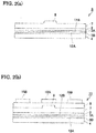
Fig. 2(a) shows the state that a ridge-typeoptical waveguide 8 is formed on theoptical waveguide material 7, andFig. 2(b) shows the state thatmodulation electrodes optical modulator 11. -
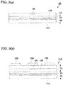
Fig. 3(a) shows a bondedbody 6A of the supportingsubstrate 4 and anoptical waveguide material 7A, andFig. 3(b) shows anoptical modulator 11A. -
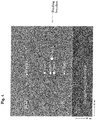
Fig. 4 is a photograph showing a cross section of an essential part of a bonded body. -
Figs. 1 and2 show an optical modulator and a bonded body for the optical modulator according to an embodiment of the present invention. - As shown in
Fig. 1(a) , it is provided afirst oxide film 3A on anoptical waveguide material 1 through anintermediate layer 2. Then, neutralized atomic beam is irradiated onto a surface of afirst oxide film 3A as an arrow A to provide an activatedsurface 12A. Further, as shown inFig. 1(b) , asecond oxide film 3B is provided on the supportingsubstrate 4. Then, neutralized atomic beam is irradiated onto a surface of asecond oxide film 3B as an arrow B to provide an activatedsurface 12B. Then, the activatedsurface 12A of thefirst oxide film 3A and activatedsurface 12B of thesecond oxide film 3B are contacted and directly bonded with each other to obtain a bonded body shown inFig. 1(c) . The first oxide film and second oxide film are integrated to form a bonding layer. - Then, as shown in
Fig. 2(a) , it is obtained anoptical waveguide material 7 having aridge part 6 by processing theoptical waveguide material 1. Here, theridge part 8 may be made a ridge-type optical waveguide, or metal ions or protons may be further diffused into theridge part 8 by metal diffusion or proton exchange method to generate an optical waveguide. 6 represents a bonded body for an optical modulator. Further, the optical waveguide may be generated only through the diffusion of the metal ions or protons. - Then, as shown in
Fig. 2(b) ,modulation electrodes optical waveguide material 7 through abuffer layer 9 to obtain anoptical modulator 11. According to the present example, as the optical waveguide material is composed of a Z-plate, theelectrodes 10A are formed directly above theoptical waveguide 8. However, the position of the electrode is appropriately changed depending on the embodiment of the optical waveguide material. - The
buffer layer 9 may be omitted in the case that an X-plate is used. - Further, according to an embodiment of
Fig.3 , metal-diffusion or proton exchangeoptical waveguide 8A is formed on the optical waveguide material to obtain anoptical waveguide material 7A and a bondedbody 6A for an optical modulator, as shown inFig. 3(a) . However, according to the present example, thefirst oxide film 3A andsecond oxide film 3B are directly bonded with each other. The first oxide film and second oxide film are integrated to form a bonding layer. Further, the ridge part is not provided in anoptical waveguide 8A. Then, as shown inFig. 3(b) , modulatingelectrodes optical waveguide material 7A through thebuffer layer 9 to obtain anoptical modulator 11A. - The respective constituents of the present invention will be described further.
- The material of the supporting substrate is made a material selected from the group consisting of magnesium oxide and a magnesium-silicon composite oxide. Magnesium oxide may be a single crystal or polycrystal. Further, the magnesium-silicon composite oxide is a composite oxide of a magnesium atom, silicon atom and oxygen atom, and may preferably be steatite (MgSiO3), forsterite (Mg2SiO4) or the mixture thereof, as a stable crystalline composition.
- The relative density of the material forming the supporting substrate may preferably be 90% or higher and may be 100%. Further, although the method of producing the supporting substrate is not particularly limited, it is preferred to improve the relative density by pressurized sintering method.
- The thickness of the optical waveguide material may preferably be 0.05 to, 5µm and more preferably be 0.1 to 1.0µm, on the viewpoint of propagation efficiency of the optical waveguide.
- The material forming the optical waveguide material is made a material selected from the group consisting of lithium niobate, lithium tantalate or lithium niobate-lithium tantalate. These materials are compatible with magnesium oxide or the magnesium-silicon composite oxide forming the supporting substrate, so that it is possible to suppress the cracks during the annealing (or film-formation of the optical waveguide material) and to provide wider bandwidth.
- The material forming the optical waveguide may preferably be expressed by LixAOz (Ais Nb, Ta), wherein x represents 0.9 to 1.05 and z represents 2.8 to 3.2. Further, 10% or less of Li and A may be replaced with other elements. As the other elements, it is listed K, Na, Rb, Cs, Be, Mg, Ca, Sr, Ba, Ti, Zr, Hf, V, Cr, Mo, W, Fe, Co, Ni, Zn, Sc, Ce or the like, and the combinations of the two or more kinds are permissible.
- The optical waveguide provided in the optical waveguide material may be so-called ridge-type optical waveguide or the metal-diffusion optical waveguide or proton exchange optical waveguide. Preferably, the diffusion type optical waveguide is formed in the ridge part by metal diffusion or proton exchange to strengthen the confinement of the light.
- It is provided an intermediate layer having a dielectric constant lower than that of the optical waveguide material on the surface of the optical waveguide material, so that the confinement of light within the optical waveguide can be made stronger. On the viewpoint, the material of the intermediate layer may preferably be silicon oxide. Further, the thickness of the intermediate layer may preferably be 2.0 to 15µm and more preferably be 4.0 to 10µm.
- According to a preferred embodiment, a first oxide film is provided on the
optical waveguide material 1, a second oxide film is provided on the supporting substrate, a surface of the first oxide film and a surface of the second oxide film are activated by neutralized atomic beam, respectively, and the respective activated surfaces are directly bonded with each other. Further, theoptical waveguide material 1 and second oxide film may be directly bonded with each other, the supporting substrate and first oxide film may be directly bonded with each other, and theoptical waveguide material 1 and supporting substrate may be directly bonded with each other. The first oxide film and second oxide film are integrated with each other to form a bonding layer. - In the surface activation by the neutralized atomic beam, preferably, the respective surfaces to be bonded are flattened to obtain flat surfaces. Here, the method of flattening the respective surfaces includes lapping and chemical mechanical polishing (CMP) or the like. Further, the flattened surface may preferably have Ra of 1nm or lower and more preferably be 0.3nm or lower.
- Then, for removing residues of a polishing agent and process denatured layer, the respective surfaces are cleaned. As the method of cleaning the surfaces, wet cleaning, dry cleaning, scrub cleaning or the like is listed, and scrub cleaning is preferred for obtaining clean surfaces simply and efficiently. At this time, after "Sun Wash LH540" is used as the cleaning agent, it is particularly preferred to perform the cleaning using mixed solution of acetone and IPA by means of a scrub cleaning machine.
- Then, neutralized beam is irradiated onto the respective surfaces to activate the respective surfaces.
- In the case that the surface activation is performed by the neutralized beam, it is used a high-speed atomic beam source of saddle-field type as a beam source. Then, an inert gas is introduced into a chamber, and a high voltage is applied on an electrode from a direct current electric power source. Electrons e are thereby moved responsive to an electric field of saddle field type generated between the electrode (positive electrode) and housing (negative electrode) to generate beams of atoms and ions of the inert gas. Among the beams reaching a grid, the ion beams are neutralized at the grid so that the beams of neutral atoms are emitted from the high-speed atomic beam source. The atomic species forming the beams may preferably be an inert gas (argon, nitrogen or the like).
- The voltage and current during the activation by the beam irradiation may preferably be made 0.5 to 2.0 kV and 50 to 200mA, respectively.
- Then, the activated surfaces are contacted and bonded with each other under vacuum atmosphere. The temperature at this time is made ambient temperature, specifically and preferably is 40°C or lower and more preferably is 30°C or lower. Further, the temperature at the time of bonding may more preferably be made 20°C or higher and 25°C or lower. The pressure during the bonding may preferably be 100 to 20000N.
- The first oxide film and second oxide film are provided for improving the bonding strength by the direct bonding. On such viewpoint, the material of each of the oxide films (material of the bonding layer) may preferably be a material selected from the group consisting of silicon oxide, magnesium oxide, alumina, tantalum pentoxide, titanium oxide and niobium pentoxide.
- Further, the thickness of each of the first oxide film and second oxide film may preferably be 2.0 pm or smaller, 1.0 pm or smaller and more preferably be 0.5 pm or smaller, on the viewpoint of the present invention. Further, the thickness of each of the first oxide film and second oxide film may preferably be 0.01 pm or larger, on the viewpoint of the present invention.
- Although the method of film-forming the intermediate layer, first oxide film or second oxide film is not limited, sputtering, chemical vapor deposition (CVD) and vapor deposition methods may be listed.
- The optical waveguide material may have a shape of a substrate as shown in
Figs. 1 to 3 . Alternatively, the optical waveguide material may be formed on the supporting substrate by film-formation. In this case, sputtering, CVD and MOCVD (organic metal vapor deposition method) are exemplified as the method of the film-formation, and a single crystal film or orientated film may be formed. Such single crystal film or orientated film may be utilized as the optical waveguide material. - An optical modulator was produced according to the method described referring to
Figs. 1 and2 . - Specifically, it was prepared an
optical waveguide material 1 composed of lithium niobate single crystal. The optical waveguide material is made of an X-plate. Then, on theoptical waveguide material 1, anintermediate layer 2 composed of silicon oxide andfirst oxide film 3A composed of amorphous silicon oxide were film-formed by sputtering in this order. The thickness of thefirst oxide film 3A was made 50 nm. - Further, on a supporting
substrate 4 composed of magnesium oxide, asecond oxide film 3B composed of amorphous silicon oxide was film-formed by sputtering. The thickness of thesecond oxide film 3B was made 50 nm. - The respective surfaces of the respective oxide films were then subjected to chemical mechanical polishing (CMP) until the film thickness was made 20 to 40 nm and Ra was made 0.08 to 0.4 nm.
- Then, neutralized atomic beam was irradiated onto the surface of the first silicon oxide film and surface of the second silicon oxide film to activate and directly bond the surfaces.
- Specifically, the respective surfaces were cleaned to remove the contamination, followed by incorporation into a vacuum chamber. It was evacuated to the order of 10-6 Pa, and the high-speed atomic beam (acceleration voltage of 1kV and Ar flow rate of 27 sccm) was irradiated onto the respective surfaces for 120 seconds to activate the respective surfaces to provide the activated surfaces. Then, after the activated surface of the first oxide film and activated surface of the second oxide film were contacted with each other, they were bonded by pressurizing at 10000 N for 2 minutes.
- Further,
Fig. 4 shows a photograph of a cross section of an essential part of the bonded body (magnification of 2,000,000 folds by a transmission type electron microscope). According to the photograph, it is shown the supporting substrate, second silicon oxide film, the direct bonding interface, first silicon oxide film and intermediate layer (silicon oxide) from the bottom in the order. Further, the results of measurement of composition ratios at the respective points were shown in table 1. - Then, the
ridge part 8 was patterned on theoptical waveguide material 1 by the procedure of photolithography using a resist, and the dry etching of theoptical waveguide material 1 was performed by a milling system. The milling system was made "RF-350" supplied by Veeco and used under the conditions of a beam voltage of 300 to 700 V and beam current of 300 to 800 mA. Then, the resist part was peeled off by an organic solvent to form a ridge part having a height of 0.4 µm, a width of 2 µm and a length of 20 mm. - A titanium metal film was then deposited on the ridge part and subjected to thermal diffusion at 1000°C for 10 hours to form a titanium diffusion optical waveguide. Then, annealing process was performed at 650°C.
- The presence or absence of the cracks of the thus obtained bonded body was observed by visual evaluation.
- Further,
electrodes Table 1 Si O Ar Point 1 44.6 54.8 0.6 Point 292.2 7.4 0.5 Point 3 88.4 8.4 3.2 Point 489.7 8.1 2.2 Point 590.7 6.6 2.7 Point 694.5 4.9 0.6 - It was obtained the optical modulator and the bonded body for the optical modulator according to similar procedure as the Inventive example 1, and the presence or absence of the cracks and bandwidth were measured.
- Further, according to the present example, the supporting substrate was formed of forsterite (Mg2SiO4). Specifically, powdery raw materials of MgO and SiO2 were weighed at a predetermined ratio and then mixed, calcined and ground to obtain powdery mixture of forsterite (Mg2SiO4). Then, alumina (Al2O3) and a dispersing agent were added to the powdery mixture and mixed and dried in ethanol. Then, a binder and acetone were added to the thus obtained powdery mixture, which was then subjected to hot water drying and sieving to obtain powder having a grain size of about 100 µm. Further, the powder was filled in a metal mold, and a column-shaped molded body of a wafer shape was molded using a uniaxial pressing machine. It was then subjected to CIP processing (cold isostatic pressing process) and then sintered at a predetermined temperature (1300 to 1400°C) to obtain a column-shaped supporting substrate composed of an oxide sintered body.
- It was obtained the optical modulator and the bonded body for the optical modulator according to the similar procedure as the inventive example 1, and the presence or absence of the cracks and bandwidth were measured.
- However, according to the present example, the supporting substrate was formed of steatite (MgSiO3), Specifically, powdery raw materials of MgO and SiO2 were weighed at a predetermined ratio and then mixed, calcined and ground to obtain mixed powder of steatite (MgSiO3). Then, alumina (Al2O3) and a dispersing agent were added to the powdery mixture and mixed and dried in ethanol. Then, a binder and acetone were added to the thus obtained powdery mixture, which was then subjected to hot water drying and sieving to obtain powder having a grain size of about 100 µm. Further, the powder was filled in a metal mold, and a column-shaped molded body of a wafer shape was molded using a uniaxial pressing machine. It was then subjected to CIP processing (cold isostatic pressing process) and then sintered at a predetermined temperature (1300 to 1400°C) to obtain a column-shaped supporting substrate composed of an oxide sintered body.
- It was obtained the optical modulator and bonded body for the optical modulator according to the similar procedure as the inventive example 1, and the presence or absence of the cracks and bandwidth were measured.
- However, the material of the supporting substrate was made a glass (quartz glass). The other procedure was the same as that of the inventive example 1.
- It was obtained the optical modulator and bonded body for the optical modulator according to the same procedure as the inventive example 1, and the presence or absence of the cracks and bandwidth were measured.
- Further, the material of the supporting substrate was made lithium niobate. The other procedure was made the same as that of the inventive example 1.
Table 2 Optical waveguide substrate Intermediate layer Bonding layer Supporting Substrate Cracks during annealing (650°C) Optical characteristics ( Bandwidth)
Inventive Example 1 X-LiNbO3 SiO2 α-Si/α-Si MgO None 1.15 Inventive Example 2 X-LiNbO3 SiO2 α-Si/α-Si Mg2SiO4 None 1.30 Inventive Example 3 X-LiNbO3 SiO2 α-Si/α-Si MgSiO3 None 1.25 Comparative Example 1 X-LiNbO3 SiO2 α-Si/α-Si glass Present --- Comparative Example 2 X-LiNbO3 SiO2 α-Si/α- Si LiNbO3 None 1 - As can be seen from table 2, according to the examples of the present invention, the cracks during the annealing was not observed and the optical characteristics were good.
- According to the comparative example 1, as it was used a supporting substrate made of the glass, the cracks during the annealing was observed.
- According to the comparative example 2, the bandwidth was proved to be inferior compared with those of the inventive examples.
Claims (10)
- A bonded body for an optical modulator, said bonded body comprising:a supporting substrate;an optical waveguide material provided on said supporting substrate and comprising a material selected from the group consisting of lithium niobate, lithium tantalate and lithium niobate-lithium tantalate; andan optical waveguide in said optical waveguide material,wherein said supporting substrate comprises a material selected from the group consisting of magnesium oxide and a magnesium-silicon composite oxide.
- The bonded body for the optical modulator of claim 1, wherein said magnesium-silicon composite oxide comprises steatite or forsterite.
- The bonded body for the optical modulator of claim 1 or 2, further comprising a bonding layer between said supporting substrate and said optical waveguide material.
- The bonded body for the optical modulator of claim 3, wherein said bonding layer comprises an oxide film.
- An optical modulator comprising:the bonded body for the optical modulator of any one of claims 1 to 4; andan electrode provided on said optical waveguide material and modulating a light propagating in said optical waveguide.
- A method of producing a bonded body for an optical modulator, said method comprising the steps of:bonding a supporting substrate comprising a material selected from the group consisting of magnesium oxide and a magnesium-silicon composite oxide and an optical waveguide material comprising a material selected from the group consisting of lithium niobate, lithium tantalate and lithium niobate-lithium tantalate; andproviding an optical waveguide in said optical waveguide material.
- The method of claim 5, wherein said magnesium-silicon composite oxide comprises steatite or forsterite.
- The method of claim 5 or 6, further comprising the step of providing a bonding layer between said supporting substrate and said optical waveguide material.
- The method of any one of claims 6 to 8, further comprising the steps of:forming a first oxide film on said optical waveguide material;forming a second oxide film on said supporting substrate; and
directly bonding said first oxide film and said second oxide film. - The method of claim 9, further comprising the steps of:irradiating a neutralized atomic beam on a surface of said first oxide film to provide a first activated surface; andirradiating a neutralized atomic beam on a surface of said second oxide film to provide a second activated surface,wherein said first activated surface and said second activated surface are directly bonded with each other.
Applications Claiming Priority (1)
| Application Number | Priority Date | Filing Date | Title |
|---|---|---|---|
| JP2019183583A JP7343347B2 (en) | 2019-10-04 | 2019-10-04 | Optical modulator conjugate, method for manufacturing optical modulator and optical modulator conjugate |
Publications (2)
| Publication Number | Publication Date |
|---|---|
| EP3800501A1 true EP3800501A1 (en) | 2021-04-07 |
| EP3800501B1 EP3800501B1 (en) | 2025-08-20 |
Family
ID=72744559
Family Applications (1)
| Application Number | Title | Priority Date | Filing Date |
|---|---|---|---|
| EP20199651.9A Active EP3800501B1 (en) | 2019-10-04 | 2020-10-01 | Bonded bodies for optical modulators, optical modulators and a method of producing bonded bodies for optical modulators |
Country Status (4)
| Country | Link |
|---|---|
| US (1) | US11448907B2 (en) |
| EP (1) | EP3800501B1 (en) |
| JP (1) | JP7343347B2 (en) |
| CN (1) | CN112612149B (en) |
Families Citing this family (7)
| Publication number | Priority date | Publication date | Assignee | Title |
|---|---|---|---|---|
| US12282214B2 (en) | 2019-11-27 | 2025-04-22 | HyperLight Corporation | Thin film lithium niobate optical device having an engineered substrate for heterogeneous integration |
| US12601938B2 (en) | 2019-11-27 | 2026-04-14 | HyperLight Corporation | Electro-optic devices having closely spaced engineered electrodes |
| EP4158422A4 (en) * | 2020-06-02 | 2024-07-17 | Hyperlight Corporation | HIGH PERFORMANCE OPTICAL MODULATORS AND DRIVERS |
| US12422726B2 (en) * | 2022-05-25 | 2025-09-23 | Optilab, Llc | Method of making thin film lithium niobate electro-optical modulators |
| CN115774300A (en) * | 2022-12-05 | 2023-03-10 | 华中光电技术研究所(中国船舶集团有限公司第七一七研究所) | Hetero-integrated silicon-based thin film lithium niobate modulator and manufacturing method thereof |
| CN121002433A (en) * | 2023-02-14 | 2025-11-21 | 国立大学法人九州大学 | Structures, waveguides, optical modulators, and methods for manufacturing structures |
| JP2026002380A (en) * | 2024-06-21 | 2026-01-08 | 株式会社日本製鋼所 | Optical waveguide bonded substrate and method for manufacturing optical waveguide bonded substrate |
Citations (5)
| Publication number | Priority date | Publication date | Assignee | Title |
|---|---|---|---|---|
| JPS6418121A (en) | 1987-07-13 | 1989-01-20 | Nippon Telegraph & Telephone | Production of high-speed optical circuit parts |
| JP2007182335A (en) * | 2006-01-05 | 2007-07-19 | Toshiba Ceramics Co Ltd | Single crystal thin film and method for forming the same |
| JP4667932B2 (en) | 2005-03-31 | 2011-04-13 | 住友大阪セメント株式会社 | Light modulator |
| JP2014147054A (en) * | 2013-01-30 | 2014-08-14 | Sumitomo Electric Ind Ltd | Piezoelectric substrate and surface acoustic wave element |
| JP2015014716A (en) | 2013-07-05 | 2015-01-22 | Tdk株式会社 | Optical waveguide and electro-optic device |
Family Cites Families (15)
| Publication number | Priority date | Publication date | Assignee | Title |
|---|---|---|---|---|
| KR0134763B1 (en) * | 1992-04-21 | 1998-04-23 | 다니이 아끼오 | Optical waveguide device and manufacturing method |
| US6544431B2 (en) | 2001-01-16 | 2003-04-08 | Triquint Technology Holding Co. | Thin film lithium niobate structure and method of making the same |
| CN1936629A (en) * | 2002-05-31 | 2007-03-28 | 松下电器产业株式会社 | Optical element and its manufacturing method |
| JP2004295088A (en) | 2003-03-11 | 2004-10-21 | Ngk Insulators Ltd | Wavelength conversion element |
| CN100538445C (en) * | 2007-11-01 | 2009-09-09 | 浙江大学 | Epitaxial barium strontium niobate thin film with transparent conductive lithium nickelate bottom electrode and preparation method |
| JP5258786B2 (en) | 2007-11-20 | 2013-08-07 | ローム株式会社 | Light control device and light control system |
| US8765621B2 (en) * | 2008-11-25 | 2014-07-01 | Ube Industries, Ltd. | Dielectric ceramic composition for high-frequency use and method for producing the same, as well as dielectric ceramic for high-frequency use and method for producing the same and high-frequency circuit element using the same |
| JP5462837B2 (en) * | 2011-06-24 | 2014-04-02 | 株式会社アドバンテスト | Optical device or light modulator |
| EP2899515A4 (en) | 2012-09-24 | 2016-05-18 | Ngk Insulators Ltd | Terahertz-wave detection element, production method therefor, joined body, and observation device |
| EP2787638B1 (en) * | 2012-11-14 | 2016-03-30 | NGK Insulators, Ltd. | Composite substrate |
| WO2016031712A1 (en) * | 2014-08-26 | 2016-03-03 | 日本碍子株式会社 | Grating element |
| US10678072B2 (en) * | 2018-01-22 | 2020-06-09 | Honeywell International Inc. | Apparatuses and methods for low energy data modulation |
| WO2019180922A1 (en) | 2018-03-23 | 2019-09-26 | 日本碍子株式会社 | Composite substrate for electro-optical device |
| WO2020080465A1 (en) * | 2018-10-19 | 2020-04-23 | 株式会社村田製作所 | Elastic wave device |
| US11226538B2 (en) * | 2019-03-07 | 2022-01-18 | California Institute Of Technology | Thin-film optical parametric oscillators |
-
2019
- 2019-10-04 JP JP2019183583A patent/JP7343347B2/en active Active
-
2020
- 2020-09-27 CN CN202011031274.9A patent/CN112612149B/en active Active
- 2020-10-01 EP EP20199651.9A patent/EP3800501B1/en active Active
- 2020-10-02 US US17/061,955 patent/US11448907B2/en active Active
Patent Citations (5)
| Publication number | Priority date | Publication date | Assignee | Title |
|---|---|---|---|---|
| JPS6418121A (en) | 1987-07-13 | 1989-01-20 | Nippon Telegraph & Telephone | Production of high-speed optical circuit parts |
| JP4667932B2 (en) | 2005-03-31 | 2011-04-13 | 住友大阪セメント株式会社 | Light modulator |
| JP2007182335A (en) * | 2006-01-05 | 2007-07-19 | Toshiba Ceramics Co Ltd | Single crystal thin film and method for forming the same |
| JP2014147054A (en) * | 2013-01-30 | 2014-08-14 | Sumitomo Electric Ind Ltd | Piezoelectric substrate and surface acoustic wave element |
| JP2015014716A (en) | 2013-07-05 | 2015-01-22 | Tdk株式会社 | Optical waveguide and electro-optic device |
Also Published As
| Publication number | Publication date |
|---|---|
| JP7343347B2 (en) | 2023-09-12 |
| JP2021060479A (en) | 2021-04-15 |
| US20210103164A1 (en) | 2021-04-08 |
| US11448907B2 (en) | 2022-09-20 |
| CN112612149A (en) | 2021-04-06 |
| CN112612149B (en) | 2024-03-29 |
| EP3800501B1 (en) | 2025-08-20 |
Similar Documents
| Publication | Publication Date | Title |
|---|---|---|
| EP3800501B1 (en) | Bonded bodies for optical modulators, optical modulators and a method of producing bonded bodies for optical modulators | |
| DE112019002430B4 (en) | Connected body and acoustic wave element | |
| KR102753300B1 (en) | Thin film electro-optical waveguide modulator device | |
| US11133788B2 (en) | Bonded body and elastic wave element | |
| EP1025580A2 (en) | Improved process for production of thin layers of semiconductor material | |
| DE112017005977B4 (en) | composite body | |
| Howlader et al. | Investigation of the bonding strength and interface current of p-Si/n-GaAs wafers bonded by surface activated bonding at room temperature | |
| DE112019001960B4 (en) | Bonded body composed of a substrate made of a piezoelectric material and a supporting substrate | |
| CN115516368B (en) | Composite substrates for electro-optical components | |
| US20240322777A1 (en) | Method for producing composite substrate | |
| CN113764572A (en) | Preparation method of heterogeneous single crystal film for acoustic filter | |
| KR102840339B1 (en) | Composite substrate, elastic surface wave element and method for manufacturing composite substrate | |
| US11920256B2 (en) | Method for growing rare earth oxide crystal on a semiconductor substrate | |
| CN112864006B (en) | Preparation method of semiconductor substrate | |
| JPWO2001001190A1 (en) | Electro-optical element and its manufacturing method | |
| US20260126479A1 (en) | Vapor Cells Having Optical Windows with Multilayer Coatings | |
| JPH06305888A (en) | Thin-film waveguide crystal and its production | |
| TWI918671B (en) | Thin-film electro-optical waveguide modulator device and methods of forming the same | |
| DE112024002769T5 (en) | COMPOSITE WAFER AND METHOD FOR MAKING A COMPOSITE WAFER | |
| Talneau et al. | Heteroepitaxial bonding of GalnAs quantum wells on Si: A new approach towards photonic integration on Si for devices operating at 1.55 µm | |
| Mazzalai et al. | Developing production process for high performance piezoelectrics in MEMS applications | |
| Maid | 7455. Structure and superconducting properties of YBa2Cn307 _ x films pre-pared by nitrogen laser evaporation and CO2 laser annealing in oxygen |
Legal Events
| Date | Code | Title | Description |
|---|---|---|---|
| PUAI | Public reference made under article 153(3) epc to a published international application that has entered the european phase |
Free format text: ORIGINAL CODE: 0009012 |
|
| STAA | Information on the status of an ep patent application or granted ep patent |
Free format text: STATUS: REQUEST FOR EXAMINATION WAS MADE |
|
| 17P | Request for examination filed |
Effective date: 20201001 |
|
| AK | Designated contracting states |
Kind code of ref document: A1 Designated state(s): AL AT BE BG CH CY CZ DE DK EE ES FI FR GB GR HR HU IE IS IT LI LT LU LV MC MK MT NL NO PL PT RO RS SE SI SK SM TR |
|
| AX | Request for extension of the european patent |
Extension state: BA ME |
|
| RBV | Designated contracting states (corrected) |
Designated state(s): AL AT BE BG CH CY CZ DE DK EE ES FI FR GB GR HR HU IE IS IT LI LT LU LV MC MK MT NL NO PL PT RO RS SE SI SK SM TR |
|
| STAA | Information on the status of an ep patent application or granted ep patent |
Free format text: STATUS: EXAMINATION IS IN PROGRESS |
|
| 17Q | First examination report despatched |
Effective date: 20230131 |
|
| GRAP | Despatch of communication of intention to grant a patent |
Free format text: ORIGINAL CODE: EPIDOSNIGR1 |
|
| STAA | Information on the status of an ep patent application or granted ep patent |
Free format text: STATUS: GRANT OF PATENT IS INTENDED |
|
| INTG | Intention to grant announced |
Effective date: 20250311 |
|
| RIN1 | Information on inventor provided before grant (corrected) |
Inventor name: KOBAYASHI, HIROHARU Inventor name: HISHIKI, TATSUYA Inventor name: KOBAYASHI, YOSHIMASA Inventor name: KONDO, JUNGO Inventor name: UNO, YUDAI Inventor name: TAI, TOMOYOSHI |
|
| GRAS | Grant fee paid |
Free format text: ORIGINAL CODE: EPIDOSNIGR3 |
|
| GRAA | (expected) grant |
Free format text: ORIGINAL CODE: 0009210 |
|
| STAA | Information on the status of an ep patent application or granted ep patent |
Free format text: STATUS: THE PATENT HAS BEEN GRANTED |
|
| AK | Designated contracting states |
Kind code of ref document: B1 Designated state(s): AL AT BE BG CH CY CZ DE DK EE ES FI FR GB GR HR HU IE IS IT LI LT LU LV MC MK MT NL NO PL PT RO RS SE SI SK SM TR |
|
| REG | Reference to a national code |
Ref country code: GB Ref legal event code: FG4D |
|
| REG | Reference to a national code |
Ref country code: CH Ref legal event code: EP |
|
| REG | Reference to a national code |
Ref country code: IE Ref legal event code: FG4D |
|
| REG | Reference to a national code |
Ref country code: DE Ref legal event code: R096 Ref document number: 602020056860 Country of ref document: DE |
|
| REG | Reference to a national code |
Ref country code: CH Ref legal event code: U11 Free format text: ST27 STATUS EVENT CODE: U-0-0-U10-U11 (AS PROVIDED BY THE NATIONAL OFFICE) Effective date: 20251101 |
|
| REG | Reference to a national code |
Ref country code: NL Ref legal event code: MP Effective date: 20250820 |
|
| PG25 | Lapsed in a contracting state [announced via postgrant information from national office to epo] |
Ref country code: IS Free format text: LAPSE BECAUSE OF FAILURE TO SUBMIT A TRANSLATION OF THE DESCRIPTION OR TO PAY THE FEE WITHIN THE PRESCRIBED TIME-LIMIT Effective date: 20251220 |
|
| PGFP | Annual fee paid to national office [announced via postgrant information from national office to epo] |
Ref country code: DE Payment date: 20250910 Year of fee payment: 6 |
|
| PG25 | Lapsed in a contracting state [announced via postgrant information from national office to epo] |
Ref country code: NO Free format text: LAPSE BECAUSE OF FAILURE TO SUBMIT A TRANSLATION OF THE DESCRIPTION OR TO PAY THE FEE WITHIN THE PRESCRIBED TIME-LIMIT Effective date: 20251120 |
|
| REG | Reference to a national code |
Ref country code: LT Ref legal event code: MG9D |
|
| PG25 | Lapsed in a contracting state [announced via postgrant information from national office to epo] |
Ref country code: PT Free format text: LAPSE BECAUSE OF FAILURE TO SUBMIT A TRANSLATION OF THE DESCRIPTION OR TO PAY THE FEE WITHIN THE PRESCRIBED TIME-LIMIT Effective date: 20251222 |
|
| PG25 | Lapsed in a contracting state [announced via postgrant information from national office to epo] |
Ref country code: FI Free format text: LAPSE BECAUSE OF FAILURE TO SUBMIT A TRANSLATION OF THE DESCRIPTION OR TO PAY THE FEE WITHIN THE PRESCRIBED TIME-LIMIT Effective date: 20250820 |
|
| PG25 | Lapsed in a contracting state [announced via postgrant information from national office to epo] |
Ref country code: NL Free format text: LAPSE BECAUSE OF FAILURE TO SUBMIT A TRANSLATION OF THE DESCRIPTION OR TO PAY THE FEE WITHIN THE PRESCRIBED TIME-LIMIT Effective date: 20250820 Ref country code: HR Free format text: LAPSE BECAUSE OF FAILURE TO SUBMIT A TRANSLATION OF THE DESCRIPTION OR TO PAY THE FEE WITHIN THE PRESCRIBED TIME-LIMIT Effective date: 20250820 |
|
| PG25 | Lapsed in a contracting state [announced via postgrant information from national office to epo] |
Ref country code: GR Free format text: LAPSE BECAUSE OF FAILURE TO SUBMIT A TRANSLATION OF THE DESCRIPTION OR TO PAY THE FEE WITHIN THE PRESCRIBED TIME-LIMIT Effective date: 20251121 |
|
| PGFP | Annual fee paid to national office [announced via postgrant information from national office to epo] |
Ref country code: CH Payment date: 20251101 Year of fee payment: 6 |
|
| PG25 | Lapsed in a contracting state [announced via postgrant information from national office to epo] |
Ref country code: SE Free format text: LAPSE BECAUSE OF FAILURE TO SUBMIT A TRANSLATION OF THE DESCRIPTION OR TO PAY THE FEE WITHIN THE PRESCRIBED TIME-LIMIT Effective date: 20250820 |
|
| PG25 | Lapsed in a contracting state [announced via postgrant information from national office to epo] |
Ref country code: LV Free format text: LAPSE BECAUSE OF FAILURE TO SUBMIT A TRANSLATION OF THE DESCRIPTION OR TO PAY THE FEE WITHIN THE PRESCRIBED TIME-LIMIT Effective date: 20250820 |
|
| PG25 | Lapsed in a contracting state [announced via postgrant information from national office to epo] |
Ref country code: PL Free format text: LAPSE BECAUSE OF FAILURE TO SUBMIT A TRANSLATION OF THE DESCRIPTION OR TO PAY THE FEE WITHIN THE PRESCRIBED TIME-LIMIT Effective date: 20250820 Ref country code: BG Free format text: LAPSE BECAUSE OF FAILURE TO SUBMIT A TRANSLATION OF THE DESCRIPTION OR TO PAY THE FEE WITHIN THE PRESCRIBED TIME-LIMIT Effective date: 20250820 |
|
| PG25 | Lapsed in a contracting state [announced via postgrant information from national office to epo] |
Ref country code: RS Free format text: LAPSE BECAUSE OF FAILURE TO SUBMIT A TRANSLATION OF THE DESCRIPTION OR TO PAY THE FEE WITHIN THE PRESCRIBED TIME-LIMIT Effective date: 20251120 |
|
| PG25 | Lapsed in a contracting state [announced via postgrant information from national office to epo] |
Ref country code: ES Free format text: LAPSE BECAUSE OF FAILURE TO SUBMIT A TRANSLATION OF THE DESCRIPTION OR TO PAY THE FEE WITHIN THE PRESCRIBED TIME-LIMIT Effective date: 20250820 |
|
| REG | Reference to a national code |
Ref country code: AT Ref legal event code: MK05 Ref document number: 1827913 Country of ref document: AT Kind code of ref document: T Effective date: 20250820 |
|
| PG25 | Lapsed in a contracting state [announced via postgrant information from national office to epo] |
Ref country code: RO Free format text: LAPSE BECAUSE OF FAILURE TO SUBMIT A TRANSLATION OF THE DESCRIPTION OR TO PAY THE FEE WITHIN THE PRESCRIBED TIME-LIMIT Effective date: 20250820 |
|
| PG25 | Lapsed in a contracting state [announced via postgrant information from national office to epo] |
Ref country code: SM Free format text: LAPSE BECAUSE OF FAILURE TO SUBMIT A TRANSLATION OF THE DESCRIPTION OR TO PAY THE FEE WITHIN THE PRESCRIBED TIME-LIMIT Effective date: 20250820 |
|
| PG25 | Lapsed in a contracting state [announced via postgrant information from national office to epo] |
Ref country code: DK Free format text: LAPSE BECAUSE OF FAILURE TO SUBMIT A TRANSLATION OF THE DESCRIPTION OR TO PAY THE FEE WITHIN THE PRESCRIBED TIME-LIMIT Effective date: 20250820 |
|
| PG25 | Lapsed in a contracting state [announced via postgrant information from national office to epo] |
Ref country code: AT Free format text: LAPSE BECAUSE OF FAILURE TO SUBMIT A TRANSLATION OF THE DESCRIPTION OR TO PAY THE FEE WITHIN THE PRESCRIBED TIME-LIMIT Effective date: 20250820 |
|
| PG25 | Lapsed in a contracting state [announced via postgrant information from national office to epo] |
Ref country code: IT Free format text: LAPSE BECAUSE OF FAILURE TO SUBMIT A TRANSLATION OF THE DESCRIPTION OR TO PAY THE FEE WITHIN THE PRESCRIBED TIME-LIMIT Effective date: 20250820 |
|
| PG25 | Lapsed in a contracting state [announced via postgrant information from national office to epo] |
Ref country code: CZ Free format text: LAPSE BECAUSE OF FAILURE TO SUBMIT A TRANSLATION OF THE DESCRIPTION OR TO PAY THE FEE WITHIN THE PRESCRIBED TIME-LIMIT Effective date: 20250820 |
|
| PG25 | Lapsed in a contracting state [announced via postgrant information from national office to epo] |
Ref country code: EE Free format text: LAPSE BECAUSE OF FAILURE TO SUBMIT A TRANSLATION OF THE DESCRIPTION OR TO PAY THE FEE WITHIN THE PRESCRIBED TIME-LIMIT Effective date: 20250820 Ref country code: SK Free format text: LAPSE BECAUSE OF FAILURE TO SUBMIT A TRANSLATION OF THE DESCRIPTION OR TO PAY THE FEE WITHIN THE PRESCRIBED TIME-LIMIT Effective date: 20250820 |