EP3799384B1 - Verfahren zur einführung von personalisierungsdaten in nichtflüchtigen speichern einer vielzahl von integrierten schaltungen, insbesondere in integrierten schaltkarten, zugehöriges system und computerprogrammprodukt - Google Patents
Verfahren zur einführung von personalisierungsdaten in nichtflüchtigen speichern einer vielzahl von integrierten schaltungen, insbesondere in integrierten schaltkarten, zugehöriges system und computerprogrammprodukt Download PDFInfo
- Publication number
- EP3799384B1 EP3799384B1 EP20196213.1A EP20196213A EP3799384B1 EP 3799384 B1 EP3799384 B1 EP 3799384B1 EP 20196213 A EP20196213 A EP 20196213A EP 3799384 B1 EP3799384 B1 EP 3799384B1
- Authority
- EP
- European Patent Office
- Prior art keywords
- data
- personalization
- memory
- image
- integrated circuit
- Prior art date
- Legal status (The legal status is an assumption and is not a legal conclusion. Google has not performed a legal analysis and makes no representation as to the accuracy of the status listed.)
- Active
Links
Images


Classifications
-
- G—PHYSICS
- G01—MEASURING; TESTING
- G01R—MEASURING ELECTRIC VARIABLES; MEASURING MAGNETIC VARIABLES
- G01R31/00—Arrangements for testing electric properties; Arrangements for locating electric faults; Arrangements for electrical testing characterised by what is being tested not provided for elsewhere
- G01R31/28—Testing of electronic circuits, e.g. by signal tracer
- G01R31/2851—Testing of integrated circuits [IC]
- G01R31/2896—Testing of IC packages; Test features related to IC packages
-
- H—ELECTRICITY
- H04—ELECTRIC COMMUNICATION TECHNIQUE
- H04W—WIRELESS COMMUNICATION NETWORKS
- H04W12/00—Security arrangements; Authentication; Protecting privacy or anonymity
- H04W12/40—Security arrangements using identity modules
-
- G—PHYSICS
- G01—MEASURING; TESTING
- G01R—MEASURING ELECTRIC VARIABLES; MEASURING MAGNETIC VARIABLES
- G01R31/00—Arrangements for testing electric properties; Arrangements for locating electric faults; Arrangements for electrical testing characterised by what is being tested not provided for elsewhere
- G01R31/28—Testing of electronic circuits, e.g. by signal tracer
- G01R31/2851—Testing of integrated circuits [IC]
- G01R31/2855—Environmental, reliability or burn-in testing
- G01R31/2856—Internal circuit aspects, e.g. built-in test features; Test chips; Measuring material aspects, e.g. electro migration [EM]
-
- G—PHYSICS
- G01—MEASURING; TESTING
- G01R—MEASURING ELECTRIC VARIABLES; MEASURING MAGNETIC VARIABLES
- G01R31/00—Arrangements for testing electric properties; Arrangements for locating electric faults; Arrangements for electrical testing characterised by what is being tested not provided for elsewhere
- G01R31/28—Testing of electronic circuits, e.g. by signal tracer
- G01R31/317—Testing of digital circuits
- G01R31/3181—Functional testing
- G01R31/3183—Generation of test inputs, e.g. test vectors, patterns or sequences
-
- G—PHYSICS
- G06—COMPUTING OR CALCULATING; COUNTING
- G06F—ELECTRIC DIGITAL DATA PROCESSING
- G06F21/00—Security arrangements for protecting computers, components thereof, programs or data against unauthorised activity
- G06F21/70—Protecting specific internal or peripheral components, in which the protection of a component leads to protection of the entire computer
- G06F21/71—Protecting specific internal or peripheral components, in which the protection of a component leads to protection of the entire computer to assure secure computing or processing of information
- G06F21/77—Protecting specific internal or peripheral components, in which the protection of a component leads to protection of the entire computer to assure secure computing or processing of information in smart cards
-
- G—PHYSICS
- G06—COMPUTING OR CALCULATING; COUNTING
- G06Q—INFORMATION AND COMMUNICATION TECHNOLOGY [ICT] SPECIALLY ADAPTED FOR ADMINISTRATIVE, COMMERCIAL, FINANCIAL, MANAGERIAL OR SUPERVISORY PURPOSES; SYSTEMS OR METHODS SPECIALLY ADAPTED FOR ADMINISTRATIVE, COMMERCIAL, FINANCIAL, MANAGERIAL OR SUPERVISORY PURPOSES, NOT OTHERWISE PROVIDED FOR
- G06Q20/00—Payment architectures, schemes or protocols
- G06Q20/30—Payment architectures, schemes or protocols characterised by the use of specific devices or networks
- G06Q20/32—Payment architectures, schemes or protocols characterised by the use of specific devices or networks using wireless devices
- G06Q20/322—Aspects of commerce using mobile devices [M-devices]
- G06Q20/3229—Use of the SIM of a M-device as secure element
-
- G—PHYSICS
- G06—COMPUTING OR CALCULATING; COUNTING
- G06Q—INFORMATION AND COMMUNICATION TECHNOLOGY [ICT] SPECIALLY ADAPTED FOR ADMINISTRATIVE, COMMERCIAL, FINANCIAL, MANAGERIAL OR SUPERVISORY PURPOSES; SYSTEMS OR METHODS SPECIALLY ADAPTED FOR ADMINISTRATIVE, COMMERCIAL, FINANCIAL, MANAGERIAL OR SUPERVISORY PURPOSES, NOT OTHERWISE PROVIDED FOR
- G06Q20/00—Payment architectures, schemes or protocols
- G06Q20/30—Payment architectures, schemes or protocols characterised by the use of specific devices or networks
- G06Q20/34—Payment architectures, schemes or protocols characterised by the use of specific devices or networks using cards, e.g. integrated circuit [IC] cards or magnetic cards
- G06Q20/355—Personalisation of cards for use
-
- G—PHYSICS
- G11—INFORMATION STORAGE
- G11C—STATIC STORES
- G11C16/00—Erasable programmable read-only memories
- G11C16/02—Erasable programmable read-only memories electrically programmable
- G11C16/06—Auxiliary circuits, e.g. for writing into memory
- G11C16/10—Programming or data input circuits
- G11C16/14—Circuits for erasing electrically, e.g. erase voltage switching circuits
-
- G—PHYSICS
- G11—INFORMATION STORAGE
- G11C—STATIC STORES
- G11C16/00—Erasable programmable read-only memories
- G11C16/02—Erasable programmable read-only memories electrically programmable
- G11C16/06—Auxiliary circuits, e.g. for writing into memory
- G11C16/26—Sensing or reading circuits; Data output circuits
-
- G—PHYSICS
- G11—INFORMATION STORAGE
- G11C—STATIC STORES
- G11C29/00—Checking stores for correct operation ; Subsequent repair; Testing stores during standby or offline operation
- G11C29/04—Detection or location of defective memory elements, e.g. cell constructio details, timing of test signals
- G11C29/08—Functional testing, e.g. testing during refresh, power-on self testing [POST] or distributed testing
- G11C29/12—Built-in arrangements for testing, e.g. built-in self testing [BIST] or interconnection details
- G11C29/38—Response verification devices
-
- H—ELECTRICITY
- H04—ELECTRIC COMMUNICATION TECHNIQUE
- H04W—WIRELESS COMMUNICATION NETWORKS
- H04W12/00—Security arrangements; Authentication; Protecting privacy or anonymity
- H04W12/30—Security of mobile devices; Security of mobile applications
- H04W12/35—Protecting application or service provisioning, e.g. securing SIM application provisioning
-
- G—PHYSICS
- G11—INFORMATION STORAGE
- G11C—STATIC STORES
- G11C29/00—Checking stores for correct operation ; Subsequent repair; Testing stores during standby or offline operation
- G11C29/04—Detection or location of defective memory elements, e.g. cell constructio details, timing of test signals
- G11C29/08—Functional testing, e.g. testing during refresh, power-on self testing [POST] or distributed testing
- G11C29/12—Built-in arrangements for testing, e.g. built-in self testing [BIST] or interconnection details
- G11C29/38—Response verification devices
- G11C29/40—Response verification devices using compression techniques
- G11C2029/4002—Comparison of products, i.e. test results of chips or with golden chip
Definitions
- Embodiments of the present disclosure relate to solutions for introducing personalization data in non volatile memories of a plurality of integrated circuits, comprising writing in the non volatile memory of a given integrated circuit a static data image, corresponding to invariant part of non volatile memory common to said plurality of integrated circuits, and personalization data image representing data specific of the given integrated circuit.
- Embodiments of the present disclosure relate in particular to integrated circuits produced with WLCSP (Wafer Level Chip Scale Packaging) techniques, in particular integrated circuits for UICC (Universal Integrated Circuit Card) and more in particular to embedded UICC (eUICC).
- WLCSP Wafer Level Chip Scale Packaging
- UICC Universal Integrated Circuit Card
- eUICC embedded UICC
- the solution refers to generation of batches of integrated circuits, in particular integrated cards such eUICC, each personalized with the introduction of personalization data (sometimes referred to as "perso data"), e.g. encryption keys or identifiers, specific for each integrated circuit in the card.
- personalization data sometimes referred to as "perso data”
- encryption keys or identifiers specific for each integrated circuit in the card.
- WLCSP Wafer Level Chip Scale Packaging
- WLP Wafer-Level packaging
- CSP Chip Scale Packaging
- WLCSP Wafer-Level packaging
- a WLCSP package usually includes the integrated circuit die, a possible redistribution Layer (RDL) and solder balls or bumps.
- the redistribution Layer is required to route from peripherally located bond wire pads to a grid array of CSP pad locations.
- WLCSP can be a good choice for small pin count devices as a way to optimize area and cost.
- the integrated circuit can be laid out with bond-wire I/O pads on the periphery of the integrated circuit.
- a redistribution Layer can then be applied to the integrated circuit to redistribute the CSP ball pads to the desired grid spacing.
- the integrated circuit modules cannot be identical: they have to be diversified by a personalization operation to include a respective Unique identifier and/or encryption keys and other personalization data.
- eUICC embedded Universal Integrated Circuit Card
- OEM OEM
- MNO Mobile Network Operator
- EUM eUICC Manufacturer
- figure 1 it is shown a flow diagram exemplary of a known method 100 for introducing personalization data in non volatile memories of a plurality of integrated circuits, which are specifically eUICCs produced by WLCSP.
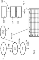
- figure 2 it is shown a schematics of an embodiment 50 of a system for introducing personalization data in non volatile memories of a plurality of integrated circuits, which can implement the method 100.
- a Mobile Network Operator 52 sends to a Chip Manufacturer 53 an input file PD with personalization data, for instance a personalization data table 11a as shown in figure 2 , to generate personalization data (e.g. IMSI, ICCID, RSA/ECC certificate, encryption keys and other identifiers, certificates or keys specific of the a specific card/chip).
- the Chip Manufacturer 53 which usually corresponds to the card vendor for integrated cards like the eUICC, may also receive from a Equipment User Manufacturer 51, i.e.
- pre-personalization data PPD which includes for instance the operative system, and other data which are common to the plurality of integrated circuits and form a static image SI, i.e. a data image, to be stored in the non volatile memory of the integrated circuit.
- the data table 11a includes a plurality of records R 1 ...R n , corresponding to the rows of the table 11a.
- Each i-th record R i corresponds to a determined i-th integrated circuit card 60 in a set or batch comprising a number n of card 60 to be personalized.
- Each column of the personalization data table 11a include then a personalization field T 1 ... T j ...T m , m being the number of fields in the table 11a and j the integer index of the personalization field, in which a different type of personalization value is stored.
- T 1 ... T m can be stored the Crypto Keys, in other fields the PIN numbers, the Unique Id and other personalization data
- the Chip Manufacturer 53 prepares in a step 120 a batch or batches of non volatile memory images I, containing static images SI, and personalization images DI to be sent to the semiconductor fabrication plant 54 producing the integrated circuits.
- the semiconductor fabrication plant 54 thus prepares in a step 130 integrated circuits 60, which are in this embodiment on wafers W, with personalized integrated circuit modules ready to be cut and soldered/embedded as eUICC in a device such as a SIM in a smartphone or tablet.
- integrated circuits 60 in general include at least a non volatile memory, in which data images can be stored for programming the integrated circuit, and usually also a processing unit, as in the case of integrated circuit card for banking and communication application, e.g. UICC and eUICC.
- the WLCSP process applied in the last step 130 described above has some constraints in providing the non volatile memory images, which have to be provided as follows:
- the non volatile memory images must be provided in S19 (also known as SREC or S-RECORD) format coded format, encrypted.
- S19 also known as SREC or S-RECORD
- the process dictates requirements such as a minimum, maximum or fixed memory slice dimension (e.g. 8 bytes) and base addresses alignment (e.g. 4 bytes).
- the memory slice is defined as a contiguous linear memory starting at a given pointer or address and spanning for a given length, in this case the dimension of 8 bytes.
- a first approach provides that personalization data, i.e. personalization images DI are bound in a dedicated memory section.
- This has the advantage that the size and position of the personalization data image can be decided at design time and overlap is intrinsically avoided.
- the drawback is that each product has its own management of personalization data, that requires a First Boot Routine (FBR) of the operating system dedicated to parse and store personalization data.
- FBR First Boot Routine
- the personalization data area may vary product by product, the first boot of modules spends time to process personalization data.
- third parties personalization applets can be an hard issue as the use of memory may be not under full control, as a matter of fact it can be unknown.
- a second known approach provides that the memory image is extracted by using a simulator. While this has the advantage of not need a physical module, the drawback is that the simulator must reproduce perfectly such physical module.
- a third known approach provides that personalization data are sent via ISO APDUs (Application Protocol Data Unit) by the Chip Manufacturer. This solution determines that Personalization Data are managed only by certified Chip Manufacturers, and also provide decoupling Pre-Personalization and Personalization steps in the case of preprocessed stocks. However, the integrated circuits have to be moved from the semiconductor plant to the chip manufacturer and the time taken by the personalization is quite slow.
- ISO APDUs Application Protocol Data Unit
- Patent application US 2016/249203 A1 discloses a method for introducing personalization data in non volatile memories of a plurality of integrated circuits comprising writing into a non volatile memory a static data image and personalization data images.
- Embodiments moreover concerns a related system for the personalization of integrated circuit cards module as well as a corresponding related computer program product, loadable in the memory of at least one computer and including software code portions for performing the steps of the method when the product is run on a computer.
- a computer program product is intended to be equivalent to reference to a computer-readable medium containing instructions for controlling a computer system to coordinate the performance of the method.
- Reference to "at least one computer” is evidently intended to highlight the possibility for the present disclosure to be implemented in a distributed/modular fashion.
- the present disclosure provides solutions regarding a method for introducing personalization data in non volatile memories of a plurality of integrated circuits, comprising
- said integrated circuit is comprised in an integrated circuit card, in particular an eUICC.
- said processing said memory locations includes identifying the memory slice at which the alteration occurs and a subsequent step of identification of the position index in the memory slice at which the alteration occurs.
- said method includes organizing said reference version of test personalization data arranged in said set of data fields in a tuple structure and that said alteration is applied on a different data field for each iteration by introducing the content of a corresponding data field in a further alteration tuple over the same set of data fields but with different data in each data field.
- said storing test personalization data in said non volatile memory includes using a personalization script comprising a sequence of commands, in particular APDU, configured to store the personalization data, said personalization script being configured to use personalization data from the reference version and one data from said further alteration tuple to apply said alteration on a different data field for each iteration by introducing the content of a corresponding data field in a further alteration tuple over the same set of data fields but with different data in each data field.
- the present disclosure provides also solutions regarding a system for introducing personalization data in non volatile memories of a plurality of integrated circuits, including a chip manufacturer and a factory, configured to introduce personalization data in non volatile memories of a plurality of integrated circuits according to the method of any of the previous claims 1 to 6.
- said chip manufacturer is configured to process said location information to identify a static memory image containing only invariant memory slices and a dynamic memory image associated to a substitution table indicating the location of memory area corresponding to each data field and to send said static and dynamic image to said factory which is configured for writing in an integrated circuit of said plurality of integrated circuits said static image and a dynamic personalized image obtained filling at corresponding locations of memory area in the dynamic memory image obtained from the substitution table the content of respective data fields in personalization data to be specifically associated to said integrated circuit .
- said factory is configured to produce said integrated circuits according to WLCSP (Wafer Level Chip Scale Packaging) techniques, performing said writing operation on integrated circuits on a wafer.
- WLCSP Wafer Level Chip Scale Packaging
- the present disclosure provides also solutions regarding a computer-program product that can be loaded into the memory of at least one processor and comprises portions of software code for implementing the method of any of the previous embodiments.
- the solution here described substantially regards a method for introducing personalization data in non volatile memories of a plurality of integrated circuits, in particular including manufacturing a plurality of chip in a WLCSCP packaging process, which comprises building static image and respective personalization data images for each integrated circuit in said plurality of integrated circuits prior storing said static image and respective personalization data images in the corresponding integrated circuit, in particular in the corresponding integrated circuit still on wafer according to the WLCSCP packaging process.
- Such building static image and respective personalization data images for each integrated circuit in said plurality of integrated circuits uses a conventional operating system, configured to be personalized by using APDU, and determined imagebuilding personalization data to obtain a set of non volatile memory images, which are processed to obtain location of memory areas that finally contain personalization data, the list of all said locations being processed to separate Static Memory Image, which contains invariant memory slices from a integrated circuit to another in the plurality of integrated circuit and a Dynamic Memory Image, which contains both invariant memory locations and target areas for personalization data for the respective integrated circuit in the plurality of integrated circuits.
- Static Memory Image which contains invariant memory slices from a integrated circuit to another in the plurality of integrated circuit
- Dynamic Memory Image which contains both invariant memory locations and target areas for personalization data for the respective integrated circuit in the plurality of integrated circuits.
- the method preferably is applied to circuits using an operating system in which memory changes not corresponding to personalization data values are not allowed outside a Transaction Buffer area.
- Such method solves the problems of the approaches discussed previously, as it does not require a personalization data dedicated area in the memory, a first boot routine with first boot execution time, allows third parties applet personalization data management. Since it is not based on simulation of course the solution does not present simulator image unreliability and also does not require moving the integrated circuits from the plant to the chip manufacturer for the personalization.
- a Full Personalization Script is provided which is a parametric script meant to configure a module once it is embedded and accessible with APDUs.
- Such Full Personalization Script includes a sequence of proper APDUs that fully personalize a product according to product requirements.
- FIG 3 it is shown an image building personalization data set AHPD, which, as shown in the following, in particular with reference to the method described in the flow diagram of figure 4 , is used to build memory images, which contains both invariant memory areas and locations and target areas for personalization data for the respective integrated circuit in the plurality of integrated circuits.
- AHPD image building personalization data set
- the image building personalization data set AHPD includes test personalization data TPD arranged in a set of data fields T 1 ...T m , in particular T 1 ...T 4 in the example. As show, this can be represented as a plurality of tuples, in particular a pair of tuples U1, U2 like in figure 3 , such that for each field T 1 ...T 4 of the two tuples the corresponding value, i.e. test personalization data value, contained in the data field is different from one tuple to the other. It is observed that also more than two tuples may be used, for instance for reliability tests.
- a set of Altered Personalization Scripts APS is built.
- Each script APS j of this set of Altered Personalization Scripts APS uses all the personalization values from the first tuple, e.g. values in fields T 1 ...T 4 of the tuple U1 except only one, and uses only one value of the second tuple U2, i.e.
- each Altered Personalization Script APS j introduces one alteration only at time, corresponding to the one selected value of the second or alteration tuple U2 corresponding to the j-th data field, in the entire data image, which is thus the j-th data image I j , to be written in the non volatile memory of the integrated circuit.
- FIG 3 a table representing the image building personalization data set AHPD, including a first o reference tuple U1, corresponding to a first profile, and a second or alteration tuple U2, corresponding to a second profile.
- the tuples can correspond to the rows of the table 11a.
- figure 4 it is shown a flow diagram representing an embodiment 200 of the method for introducing personalization data in non volatile memories of a plurality of integrated circuits here described.
- the method includes that a test integrated circuit 60' is provided in a step 205, which is the same integrated circuit of the integrated circuits 60 in the batch to be produced at the factory 54.
- the method then includes comparing in a step 240 each test dumped image I j with the test dumped image obtained from the reference version, i.e. the first test dumped image I 1 , extracting memory locations of the memory area LM j in the non volatile memory of the integrated circuit 60' at which said dumped image I j differs from the dumped image I 1 obtained from the reference version. Finally a set of memory location of memory areas LM 2 ...LM m is obtained corresponding to the target areas for personalization data for the respective integrated circuit in the plurality of integrated circuits. In a step 250 is then performed the identification through said memory locations LM j of the memory area or slices corresponding to a static memory image SI, i.e. containing only invariant memory slices MS, and to a dynamic memory image DMI, obtaining a location map ML indicating the memory areas of the non volatile memory in which the dynamic memory images DMI j corresponding to the different fields T j are to be stored .
- a step 240 each test dumped image I
- a normalization step is performed, which produces a substitution table ST indicating the slice MS of the non volatile memory 61 in which a certain target area, i.e. memory area in which the dynamic image corresponding to a certain data field is to be stored, and a position index k in such slice MS.
- a static image SI and a dynamic image DMI formed by the set of dynamic memory images DMI j corresponding to the different fields T j are made available together with such substation table ST.
- the static image SI since data are invariant, represents already the static image which will be the programmed in all the integrated circuits 60 s of the batch.
- the dynamic image represents the target area to be filled in by the actual personalization data PD.
- a step 270 the actual personalization data PD are stored in the corresponding target area of the dynamic images DMI j using the information on the location (slice MS, index k) in the substitution table ST, obtaining dynamic personalized images PMI j in the non volatile memory of the integrated circuit 60.
- this step 270 takes place when programming the WLCSP integrated circuit 60 before packaging, i.e. steps 210-260 can be performed at the Chip Manufacturer 53 at a given time obtaining the static image SI, the dynamic image DMI and the substitution table ST, while the filling step 270 can take place at the semiconductor plant 54 at a subsequent time.
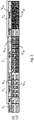
- FIG. 5-10 it is represented a non volatile memory 61 of the test integrated circuit 60', shown as a matrix in which the first column contains the memory address AD and the following columns, eight in the example, represents each a byte of a memory page or memory slice MS, i.e. a memory with 8 byte granularity.
- Target areas corresponding to data field T2, T3, T4 are shown, containing the values of the first profile, i.e. tuple U1, V 21 , V 31 , V 41 .
- Figure 7 represents the memory 61 after the second personalization, i.e. performing first step 232 to obtain an instance TPD 2 corresponding to the reference version U1 subject to an alteration applied on a different data field for each iteration, in particular said alteration being applied on the data field T 2 introducing the value V 22 of the corresponding data field, i.e. the values of the PIN code in this case from the second or further alteration tuple U2.
- the second instance TPD 2 is then stored in the storing step 233.
- Figure 8 represents the memory 61 after the second personalization, i.e. performing first step 232 to obtain an instance TPD 3 corresponding to the reference version U1 subject to an alteration applied on a different data field for each iteration, in particular said alteration being applied on the data field T 3 introducing the value V 32 of the corresponding data field, i.e. the values of the IMSI code in this case from the second or further alteration tuple U2.
- the third instance TPD 3 is then stored in the storing step 233.
- Figure 9 represents the memory 61 after the third personalization, i.e. performing first step 232 to obtain an instance TPD 4 corresponding to the reference version U1 subject to an alteration applied on a different data field for each iteration, in particular said alteration being applied on the data field T 4 introducing the value V 42 of the corresponding data field, i.e. the values of the ICCID code in this case from the second or further alteration tuple U2.
- the third instance TPD 3 is then stored in the storing step 233.
- the described solution allows thus to introduce personalization data without requiring a personalization data dedicated area in the memory, a first boot routine with first boot execution time, and allows third parties applet personalization data management. Since it is based on a test integrated circuit which is equal to those of the batch to be produced, and it is not based on simulation the solution does not present simulator image unreliability and also does not require moving the integrated circuits from the plant to the chip manufacturer for the personalization.
- the method here described in particular can be applied to the introduction of personalization data in integrated circuits for smart cards like eUICC and iUICC, but also in variant embodiments to integrated circuits for other device such as Secure Elements, NFC tags, VPP, SSP, which have a non volatile memory to be programmed with personalization data.
- the integrated circuits are produced by a WLCSP, Wafer Level Chip Scale Packaging, so that the method of introduction of personalization data here described can be performed while the integrated circuit is still on the wafer, and then it is cut and possibly soldered on a plastic support or in place in a device, however the method here described can be applied also to an integrated circuit already separated by the wafer, in particular already mounted on the support or embedded in a device.
Landscapes
- Engineering & Computer Science (AREA)
- Physics & Mathematics (AREA)
- General Physics & Mathematics (AREA)
- General Engineering & Computer Science (AREA)
- Computer Security & Cryptography (AREA)
- Computer Hardware Design (AREA)
- Business, Economics & Management (AREA)
- Theoretical Computer Science (AREA)
- Computer Networks & Wireless Communication (AREA)
- Microelectronics & Electronic Packaging (AREA)
- General Business, Economics & Management (AREA)
- Strategic Management (AREA)
- Accounting & Taxation (AREA)
- Signal Processing (AREA)
- Environmental & Geological Engineering (AREA)
- Mathematical Physics (AREA)
- Software Systems (AREA)
- Testing Or Measuring Of Semiconductors Or The Like (AREA)
- Credit Cards Or The Like (AREA)
Claims (9)
- Verfahren zur Einführung von Personalisierungsdaten in nicht flüchtigen Speichern einer Vielzahl von integrierten Schaltungen, umfassendSchreiben in dem nicht flüchtigen Speicher (61) einer gegebenen integrierten Schaltung einer statischen Datenabbildung (SI), das einem unveränderlichen Teil des nicht flüchtigen Speichers entspricht, welcher der Vielzahl von integrierten Schaltungen (60) gemein ist, die ein Betriebssystem beinhalten, und von Personalisierungsdatenabbildungen (DI), welche Daten repräsentieren, die spezifisch für die gegebene integrierte Schaltung sind,wobei die Personalisierungsdaten einer gegebenen integrierten Schaltung zugehörig sind, die in einer Reihe von Personalisierungsdatenfeldern angeordnet ist,dadurch gekennzeichnet, dass das Verfahren einen Vorgang des Erzeugens (205-235) von Prüfdatenabbildungen (Ij) beinhaltet, die in dem nicht flüchtigen Speicher abzulegen sind, umfassendfür jedes Datenfeld (Tj) in der Reihe von Personalisierungsdatenfeldern (T1...Tm) Ausführen eines iterativen Vorgangs, bei jeder Iteration die folgenden Abläufe umfassend:Löschen (210) eines nicht flüchtigen Speichers (61) einer integrierten Prüfschaltung (60') entsprechend der Vielzahl von integrierten Schaltungen,Ablegen (220) des Betriebssystems in dem nicht flüchtigen Speicher,Ablegen (230) von Prüfpersonalisierungsdaten in dem nicht flüchtigen Speicher,wobei das Ablegen (230) umfasstErzeugen (232) von Instanzen (TPD1...TPDm) der Prüfpersonalisierungsdaten (TPD) auf der Grundlage einer bereitgestellten (231) Referenzversion (U1) der Prüfpersonalisierungsdaten (TPD), die in der Reihe von Datenfeldern (T1...Tm) angeordnet sind,wobei die erste Instanz (TPD1) an der ersten Iteration der bereitgestellten Referenzversion (U1) entspricht, und die folgenden Instanzen (TPD2...TPDm) in folgenden Iterationen der Referenzversion (U1) entsprechen, die einer Änderung unterzogen wird, die für jede Iteration auf ein unterschiedliches Datenfeld (T1...Tm) angewandt wird,Deponieren (234) einer Abbildung (Ij) des nicht flüchtigen Speichers (61) entsprechend der aktuellen Prüfinstanz (TPDj),iteratives Ausführen (235) des Erzeugungsvorganges, bis das letzte Datenfeld in der Reihe von Personalisierungsdatenfeldern eine entsprechende Reihe von deponierten Prüfabbildungen (I1...Im), eines für jedes Datenfeld (Tj) in der Reihe von Personalisierungsdatenfeldern (T1...Tm) , erhält,Vergleichen (240) einer jeden deponierten Prüfabbildung (I1...Im) mit der deponierten Prüfabbildung (I1), die aus der Referenzversion (U1) erhalten wird, Extrahieren jeweiliger Standortinformationen (LMj) hinsichtlich des Speicherbereichs in dem nicht flüchtigen Speicher (61), in dem die deponierte Prüfabbildung (I1...Im) von der deponierten Prüfabbildung (I1) abweicht, die aus der Referenzversion erhalten wird,Verarbeiten (250) der Standortinformationen zum Identifizieren einer statischen Speicherabbildung (SI), die nur unveränderliche Speichersegmente enthält, und einer dynamischen Speicherabbildung (DMI), die einer Ersatztabelle (ST) zugewiesen ist, die den Standort eines Speicherbereichs anzeigt, der jedem Datenfeld (Tj) entspricht,Schreiben (270) in einer integrierten Schaltung (60) der Vielzahl von integrierten Schaltungen der statischen Abbildung (SI) und einer erhaltenen personalisierten dynamischen Abbildung (PMI), Füllen an entsprechenden Standorten eines Speicherbereichs in der dynamischen Speicherabbildung (DMI), die aus der Ersatztabelle (ST) erhalten wird, des Inhalts der jeweiligen Datenfelder (Tj) in Personalisierungsdaten (PD), die spezifisch der integrierten Schaltung (60) zuzuweisen sind.
- Verfahren nach Anspruch 1, dadurch gekennzeichnet, dass die integrierte Schaltung (60) in einer integrierten Schaltungskarte, insbesondere einer eUICC vorliegt.
- Verfahren nach Anspruch 1, dadurch gekennzeichnet, dass das Verarbeiten der Speicherstandorte (LMj) Identifizieren des Speichersegments (MS), in dem die Änderung auftritt, und einen nachfolgenden Schritt des Identifizierens des Positionsindex (k) in dem Speichersegment (MS) beinhaltet, bei dem die Änderung auftritt.
- Verfahren nach einem der vorstehenden Ansprüche, dadurch gekennzeichnet, dass es Organisieren der Referenzversion (U1) von Prüfpersonalisierungsdaten (TPD), die in der Reihe von Datenfeldern (T1...Tm) in einer Tupelstruktur beinhaltet, und dadurch, dass die Änderung für jede Iteration auf ein unterschiedliches Datenfeld durch Einbringen des Inhalts eines entsprechenden Datenfelds in einem weiteren Änderungstupel (U2) über dieselbe Reihe von Datenfeldern (T1...Tm), jedoch mit unterschiedlichen Daten in jedem Datenfeld angewandt wird.
- Verfahren nach Anspruch 4, dadurch gekennzeichnet, dass das Ablegen (230) von Prüfpersonalisierungsdaten in dem nicht flüchtigen Speicher (61) Verwenden eines Personalisierungsscripts beinhaltet, das eine Befehlsfolge, insbesondere APDU, umfasst, die konfiguriert ist, um die Personalisierungsdaten abzulegen, wobei das Personalisierungsscript konfiguriert ist, um Personalisierungsdaten aus der Referenzversion (U1) und ein Datum aus dem weiteren Änderungstupel (U2) zu verwenden, um die Änderung für jede Iteration auf ein unterschiedliches Datenfeld durch Einbringen des Inhalts eines entsprechenden Datenfelds in ein weiteres Änderungstupel (U2) über dieselbe Reihe von Datenfeldern (T1...Tm), jedoch mit unterschiedlichen Daten in jedem Datenfeld, anzuwenden.
- System zur Einführung von Personalisierungsdaten in nicht flüchtigen Speichern einer Vielzahl von integrierten Schaltungen, das einen Chip-Hersteller (53) und eine Fertigung (54) beinhaltet, die konfiguriert ist, um Personalisierungsdaten in nicht flüchtige Speicher einer Vielzahl von integrierten Schaltungen entsprechend dem Verfahren nach einem der vorstehenden Ansprüche 1 bis 5 einzubringen.
- System nach Anspruch 6, wobei der Chip-Hersteller (53) konfiguriert ist, um die Standortinformationen zu verarbeiten (250), um eine statische Speicherabbildung (SI) zu identifizieren, die nur unveränderliche Speichersegmente enthält, und eine dynamische Speicherabbildung (DMI), die einer Ersatztabelle (ST) zugewiesen ist, die den Standort eines Speicherbereichs anzeigt, der jedem Datenfeld (Tj) entspricht, und die statische (SI) und dynamische Abbildung zur Fertigung (54) zu senden, die zum Schreiben (270) in einer integrierten Schaltung (60) der Vielzahl von integrierten Schaltungen der statischen Abbildung (SI) und einer erhaltenen personalisierten dynamischen Abbildung (PMI), Füllen an entsprechenden Standorten eines Speicherbereichs in der dynamischen Speicherabbildung (DMI), die aus der Ersatztabelle (ST) erhalten wird, des Inhalts der jeweiligen Datenfelder (Tj) in Personalisierungsdaten (PD), die spezifisch der integrierten Schaltung (60) zuzuweisen sind.
- System nach den Ansprüchen 6 oder 7, wobei die Fertigung (54) konfiguriert ist, um die integrierten Schaltungen entsprechend WLCSP (Wafer-Level-Chipscale-Packaging) Techniken herzustellen, die den Schreibablauf (270) in den integrierten Schaltungen (60) auf einem Wafer (W) durchführt.
- Computerprogrammprodukt, das in den Speicher mindestens eines Prozessors geladen werden kann, und Abschnitte eines Software-Codes zum Umsetzen des Verfahrens nach einem der Ansprüche 1 bis 5 umfasst.
Applications Claiming Priority (1)
| Application Number | Priority Date | Filing Date | Title |
|---|---|---|---|
| IT102019000017561A IT201900017561A1 (it) | 2019-09-30 | 2019-09-30 | "Procedimento per introdurre dati di personalizzazione in memorie non volatile di una pluralità di circuiti integrati, in particolare in carte a circuito integrato, corrispondente sistema e prodotto informatico" |
Publications (2)
| Publication Number | Publication Date |
|---|---|
| EP3799384A1 EP3799384A1 (de) | 2021-03-31 |
| EP3799384B1 true EP3799384B1 (de) | 2022-07-06 |
Family
ID=69191193
Family Applications (1)
| Application Number | Title | Priority Date | Filing Date |
|---|---|---|---|
| EP20196213.1A Active EP3799384B1 (de) | 2019-09-30 | 2020-09-15 | Verfahren zur einführung von personalisierungsdaten in nichtflüchtigen speichern einer vielzahl von integrierten schaltungen, insbesondere in integrierten schaltkarten, zugehöriges system und computerprogrammprodukt |
Country Status (3)
| Country | Link |
|---|---|
| US (1) | US11675001B2 (de) |
| EP (1) | EP3799384B1 (de) |
| IT (1) | IT201900017561A1 (de) |
Families Citing this family (4)
| Publication number | Priority date | Publication date | Assignee | Title |
|---|---|---|---|---|
| DE102021001850A1 (de) * | 2021-04-09 | 2022-10-13 | Giesecke+Devrient Mobile Security Gmbh | Verfahren zum Personalisieren eines sicheren Elementes |
| CN113360955B (zh) * | 2021-06-16 | 2024-06-04 | 深圳市雪球科技有限公司 | 一种Applet管理方法、装置和服务器 |
| US20250245314A1 (en) * | 2022-04-22 | 2025-07-31 | Giesecke+Devrient Mobile Security Germany Gmbh | Method and system for personalizing a secure element |
| IT202200011084A1 (it) * | 2022-05-26 | 2023-11-26 | St Microelectronics Srl | Procedimento per introdurre dati di personalizzazione in memorie non volatile di una pluralità di circuiti integrati, in particolare in carte a circuito integrato, corrispondente sistema e prodotto informatico |
Family Cites Families (10)
| Publication number | Priority date | Publication date | Assignee | Title |
|---|---|---|---|---|
| US5889941A (en) * | 1996-04-15 | 1999-03-30 | Ubiq Inc. | System and apparatus for smart card personalization |
| CA2405477A1 (en) * | 2000-04-11 | 2001-10-18 | Visa International Service Association | Integrated production of smart cards |
| FR2848364B1 (fr) * | 2002-12-09 | 2005-03-11 | Oberthur Card Syst Sa | Procede de personnalisation securisee d'un objet |
| EP2016533B1 (de) * | 2006-04-28 | 2014-03-26 | Giesecke & Devrient GmbH | Verfahren und vorrichtung zur personalisierung tragbarer datenträger |
| FR3011652B1 (fr) * | 2013-10-07 | 2015-12-04 | Oberthur Technologies | Procede de personnalisation d'un element securise |
| EP2887212A1 (de) * | 2013-12-17 | 2015-06-24 | StepNexus Ltd | System, Verfahren und personalisierbare tragbare Vorrichtung mit in komprimierter Form verteilten Anwendungscodebibliotheken |
| CN112566074B (zh) * | 2015-04-10 | 2024-11-08 | 苹果公司 | 用于电子用户身份模块(esim)安装和互操作的装置和方法 |
| EP3483772A1 (de) * | 2017-11-14 | 2019-05-15 | Nagravision S.A. | Personalisierung einer integrierten schaltung durch datei die mit des ausgangs eine physikalisch unklonbarer funktion verschlüsselt sind |
| IT201800004046A1 (it) * | 2018-03-28 | 2019-09-28 | St Microelectronics Srl | Procedimento per la personalizzazione di carte a circuito integrato, corrispondente sistema e prodotto informatico |
| IT201800005510A1 (it) | 2018-05-18 | 2019-11-18 | Procedimento per la generazione di dati personalizzati di profile package in carte a circuito integrato, corrispondente sistema e prodotto informatico |
-
2019
- 2019-09-30 IT IT102019000017561A patent/IT201900017561A1/it unknown
-
2020
- 2020-09-15 EP EP20196213.1A patent/EP3799384B1/de active Active
- 2020-09-29 US US17/036,135 patent/US11675001B2/en active Active
Also Published As
| Publication number | Publication date |
|---|---|
| IT201900017561A1 (it) | 2021-03-30 |
| EP3799384A1 (de) | 2021-03-31 |
| US11675001B2 (en) | 2023-06-13 |
| US20210096178A1 (en) | 2021-04-01 |
Similar Documents
| Publication | Publication Date | Title |
|---|---|---|
| US11675001B2 (en) | Method, system and computer program product for introducing personalization data in nonvolatile memories of a plurality of integrated circuits | |
| US8447982B2 (en) | System and method for operating end-to-end security channel between server and IC card | |
| JP5910297B2 (ja) | 情報処理装置、icチップ、情報処理方法、プログラム、及び情報処理システム | |
| US9250930B2 (en) | Configuration method for an electronic entity | |
| US11907931B2 (en) | Method and system for managing virtual electronic card, secure chip, terminal and storage medium | |
| US9037687B2 (en) | Information processing apparatus, method and program for writing file system metadata of plural operating systems | |
| CN117158016A (zh) | 用于个性化安全元件的方法 | |
| CN106937275A (zh) | 一种在安卓系统下保存系统唯一标识及硬件id的设备 | |
| US10509901B2 (en) | Method of managing a secure element | |
| US12093560B2 (en) | Method for introducing personalization data in non volatile memories of a plurality of integrated circuits, in particular in integrated circuit cards, corresponding system and computer program product | |
| US8844827B2 (en) | Chip card, and method for the software-based modification of a chip card | |
| US20180107840A1 (en) | Method of restoring a secure element to a factory state | |
| US11106472B2 (en) | Method for managing multiple operating systems in integrated circuit cards, corresponding system and computer program product | |
| KR101489102B1 (ko) | 안전한 전자 토큰의 동작을 분석하는 방법 | |
| US10489775B2 (en) | Integrated circuit card adapted to transfer first data from a first application for use by a second application | |
| CN117131553A (zh) | 引入个性化数据的方法、对应系统和计算机程序产品 | |
| EP2499642B1 (de) | Verfahren zur Analyse des Verschleißes eines nichtflüchtigen Speichers, der in ein sicheres elektronisches Token eingebettet ist | |
| US20250094968A1 (en) | System and Method for Payment Hardware System Module (HSM) Integration | |
| US20240202310A1 (en) | Installation of a bound package on a security module | |
| JP6515850B2 (ja) | 情報処理装置、icチップ、情報処理方法、プログラム、及び情報処理システム | |
| HK40026914A (en) | Model training data storage method and device, electronic equipment and storage medium | |
| CN118246039A (zh) | 电子设备的保护 | |
| CN118246040A (zh) | 电子设备的保护 | |
| Olofsson | Design and Implementation of SIM Functionality for TETRA-system on a Smart Card |
Legal Events
| Date | Code | Title | Description |
|---|---|---|---|
| PUAI | Public reference made under article 153(3) epc to a published international application that has entered the european phase |
Free format text: ORIGINAL CODE: 0009012 |
|
| STAA | Information on the status of an ep patent application or granted ep patent |
Free format text: STATUS: THE APPLICATION HAS BEEN PUBLISHED |
|
| AK | Designated contracting states |
Kind code of ref document: A1 Designated state(s): AL AT BE BG CH CY CZ DE DK EE ES FI FR GB GR HR HU IE IS IT LI LT LU LV MC MK MT NL NO PL PT RO RS SE SI SK SM TR |
|
| AX | Request for extension of the european patent |
Extension state: BA ME |
|
| STAA | Information on the status of an ep patent application or granted ep patent |
Free format text: STATUS: REQUEST FOR EXAMINATION WAS MADE |
|
| 17P | Request for examination filed |
Effective date: 20210924 |
|
| RBV | Designated contracting states (corrected) |
Designated state(s): AL AT BE BG CH CY CZ DE DK EE ES FI FR GB GR HR HU IE IS IT LI LT LU LV MC MK MT NL NO PL PT RO RS SE SI SK SM TR |
|
| REG | Reference to a national code |
Ref country code: DE Ref legal event code: R079 Ref document number: 602020003869 Country of ref document: DE Free format text: PREVIOUS MAIN CLASS: H04L0029060000 Ipc: H04W0012000000 |
|
| GRAP | Despatch of communication of intention to grant a patent |
Free format text: ORIGINAL CODE: EPIDOSNIGR1 |
|
| STAA | Information on the status of an ep patent application or granted ep patent |
Free format text: STATUS: GRANT OF PATENT IS INTENDED |
|
| RIC1 | Information provided on ipc code assigned before grant |
Ipc: H04W 12/30 20210101ALI20220203BHEP Ipc: H04W 8/20 20090101ALI20220203BHEP Ipc: H04W 4/50 20180101ALI20220203BHEP Ipc: H04W 12/00 20210101AFI20220203BHEP |
|
| INTG | Intention to grant announced |
Effective date: 20220301 |
|
| GRAS | Grant fee paid |
Free format text: ORIGINAL CODE: EPIDOSNIGR3 |
|
| GRAA | (expected) grant |
Free format text: ORIGINAL CODE: 0009210 |
|
| STAA | Information on the status of an ep patent application or granted ep patent |
Free format text: STATUS: THE PATENT HAS BEEN GRANTED |
|
| AK | Designated contracting states |
Kind code of ref document: B1 Designated state(s): AL AT BE BG CH CY CZ DE DK EE ES FI FR GB GR HR HU IE IS IT LI LT LU LV MC MK MT NL NO PL PT RO RS SE SI SK SM TR |
|
| REG | Reference to a national code |
Ref country code: AT Ref legal event code: REF Ref document number: 1503741 Country of ref document: AT Kind code of ref document: T Effective date: 20220715 Ref country code: CH Ref legal event code: EP |
|
| REG | Reference to a national code |
Ref country code: DE Ref legal event code: R096 Ref document number: 602020003869 Country of ref document: DE |
|
| REG | Reference to a national code |
Ref country code: IE Ref legal event code: FG4D |
|
| REG | Reference to a national code |
Ref country code: LT Ref legal event code: MG9D |
|
| REG | Reference to a national code |
Ref country code: NL Ref legal event code: MP Effective date: 20220706 |
|
| PG25 | Lapsed in a contracting state [announced via postgrant information from national office to epo] |
Ref country code: SE Free format text: LAPSE BECAUSE OF FAILURE TO SUBMIT A TRANSLATION OF THE DESCRIPTION OR TO PAY THE FEE WITHIN THE PRESCRIBED TIME-LIMIT Effective date: 20220706 Ref country code: RS Free format text: LAPSE BECAUSE OF FAILURE TO SUBMIT A TRANSLATION OF THE DESCRIPTION OR TO PAY THE FEE WITHIN THE PRESCRIBED TIME-LIMIT Effective date: 20220706 Ref country code: PT Free format text: LAPSE BECAUSE OF FAILURE TO SUBMIT A TRANSLATION OF THE DESCRIPTION OR TO PAY THE FEE WITHIN THE PRESCRIBED TIME-LIMIT Effective date: 20221107 Ref country code: NO Free format text: LAPSE BECAUSE OF FAILURE TO SUBMIT A TRANSLATION OF THE DESCRIPTION OR TO PAY THE FEE WITHIN THE PRESCRIBED TIME-LIMIT Effective date: 20221006 Ref country code: NL Free format text: LAPSE BECAUSE OF FAILURE TO SUBMIT A TRANSLATION OF THE DESCRIPTION OR TO PAY THE FEE WITHIN THE PRESCRIBED TIME-LIMIT Effective date: 20220706 Ref country code: LV Free format text: LAPSE BECAUSE OF FAILURE TO SUBMIT A TRANSLATION OF THE DESCRIPTION OR TO PAY THE FEE WITHIN THE PRESCRIBED TIME-LIMIT Effective date: 20220706 Ref country code: LT Free format text: LAPSE BECAUSE OF FAILURE TO SUBMIT A TRANSLATION OF THE DESCRIPTION OR TO PAY THE FEE WITHIN THE PRESCRIBED TIME-LIMIT Effective date: 20220706 Ref country code: FI Free format text: LAPSE BECAUSE OF FAILURE TO SUBMIT A TRANSLATION OF THE DESCRIPTION OR TO PAY THE FEE WITHIN THE PRESCRIBED TIME-LIMIT Effective date: 20220706 Ref country code: ES Free format text: LAPSE BECAUSE OF FAILURE TO SUBMIT A TRANSLATION OF THE DESCRIPTION OR TO PAY THE FEE WITHIN THE PRESCRIBED TIME-LIMIT Effective date: 20220706 |
|
| REG | Reference to a national code |
Ref country code: AT Ref legal event code: MK05 Ref document number: 1503741 Country of ref document: AT Kind code of ref document: T Effective date: 20220706 |
|
| PG25 | Lapsed in a contracting state [announced via postgrant information from national office to epo] |
Ref country code: PL Free format text: LAPSE BECAUSE OF FAILURE TO SUBMIT A TRANSLATION OF THE DESCRIPTION OR TO PAY THE FEE WITHIN THE PRESCRIBED TIME-LIMIT Effective date: 20220706 Ref country code: IS Free format text: LAPSE BECAUSE OF FAILURE TO SUBMIT A TRANSLATION OF THE DESCRIPTION OR TO PAY THE FEE WITHIN THE PRESCRIBED TIME-LIMIT Effective date: 20221106 Ref country code: HR Free format text: LAPSE BECAUSE OF FAILURE TO SUBMIT A TRANSLATION OF THE DESCRIPTION OR TO PAY THE FEE WITHIN THE PRESCRIBED TIME-LIMIT Effective date: 20220706 Ref country code: GR Free format text: LAPSE BECAUSE OF FAILURE TO SUBMIT A TRANSLATION OF THE DESCRIPTION OR TO PAY THE FEE WITHIN THE PRESCRIBED TIME-LIMIT Effective date: 20221007 |
|
| REG | Reference to a national code |
Ref country code: DE Ref legal event code: R097 Ref document number: 602020003869 Country of ref document: DE |
|
| PG25 | Lapsed in a contracting state [announced via postgrant information from national office to epo] |
Ref country code: SM Free format text: LAPSE BECAUSE OF FAILURE TO SUBMIT A TRANSLATION OF THE DESCRIPTION OR TO PAY THE FEE WITHIN THE PRESCRIBED TIME-LIMIT Effective date: 20220706 Ref country code: RO Free format text: LAPSE BECAUSE OF FAILURE TO SUBMIT A TRANSLATION OF THE DESCRIPTION OR TO PAY THE FEE WITHIN THE PRESCRIBED TIME-LIMIT Effective date: 20220706 Ref country code: MC Free format text: LAPSE BECAUSE OF FAILURE TO SUBMIT A TRANSLATION OF THE DESCRIPTION OR TO PAY THE FEE WITHIN THE PRESCRIBED TIME-LIMIT Effective date: 20220706 Ref country code: DK Free format text: LAPSE BECAUSE OF FAILURE TO SUBMIT A TRANSLATION OF THE DESCRIPTION OR TO PAY THE FEE WITHIN THE PRESCRIBED TIME-LIMIT Effective date: 20220706 Ref country code: CZ Free format text: LAPSE BECAUSE OF FAILURE TO SUBMIT A TRANSLATION OF THE DESCRIPTION OR TO PAY THE FEE WITHIN THE PRESCRIBED TIME-LIMIT Effective date: 20220706 Ref country code: AT Free format text: LAPSE BECAUSE OF FAILURE TO SUBMIT A TRANSLATION OF THE DESCRIPTION OR TO PAY THE FEE WITHIN THE PRESCRIBED TIME-LIMIT Effective date: 20220706 |
|
| PLBE | No opposition filed within time limit |
Free format text: ORIGINAL CODE: 0009261 |
|
| STAA | Information on the status of an ep patent application or granted ep patent |
Free format text: STATUS: NO OPPOSITION FILED WITHIN TIME LIMIT |
|
| REG | Reference to a national code |
Ref country code: BE Ref legal event code: MM Effective date: 20220930 |
|
| PG25 | Lapsed in a contracting state [announced via postgrant information from national office to epo] |
Ref country code: SK Free format text: LAPSE BECAUSE OF FAILURE TO SUBMIT A TRANSLATION OF THE DESCRIPTION OR TO PAY THE FEE WITHIN THE PRESCRIBED TIME-LIMIT Effective date: 20220706 Ref country code: EE Free format text: LAPSE BECAUSE OF FAILURE TO SUBMIT A TRANSLATION OF THE DESCRIPTION OR TO PAY THE FEE WITHIN THE PRESCRIBED TIME-LIMIT Effective date: 20220706 |
|
| 26N | No opposition filed |
Effective date: 20230411 |
|
| PG25 | Lapsed in a contracting state [announced via postgrant information from national office to epo] |
Ref country code: LU Free format text: LAPSE BECAUSE OF NON-PAYMENT OF DUE FEES Effective date: 20220915 Ref country code: AL Free format text: LAPSE BECAUSE OF FAILURE TO SUBMIT A TRANSLATION OF THE DESCRIPTION OR TO PAY THE FEE WITHIN THE PRESCRIBED TIME-LIMIT Effective date: 20220706 |
|
| PG25 | Lapsed in a contracting state [announced via postgrant information from national office to epo] |
Ref country code: IE Free format text: LAPSE BECAUSE OF NON-PAYMENT OF DUE FEES Effective date: 20220915 Ref country code: FR Free format text: LAPSE BECAUSE OF NON-PAYMENT OF DUE FEES Effective date: 20220930 |
|
| PG25 | Lapsed in a contracting state [announced via postgrant information from national office to epo] |
Ref country code: SI Free format text: LAPSE BECAUSE OF FAILURE TO SUBMIT A TRANSLATION OF THE DESCRIPTION OR TO PAY THE FEE WITHIN THE PRESCRIBED TIME-LIMIT Effective date: 20220706 |
|
| PG25 | Lapsed in a contracting state [announced via postgrant information from national office to epo] |
Ref country code: BE Free format text: LAPSE BECAUSE OF NON-PAYMENT OF DUE FEES Effective date: 20220930 |
|
| PG25 | Lapsed in a contracting state [announced via postgrant information from national office to epo] |
Ref country code: IT Free format text: LAPSE BECAUSE OF FAILURE TO SUBMIT A TRANSLATION OF THE DESCRIPTION OR TO PAY THE FEE WITHIN THE PRESCRIBED TIME-LIMIT Effective date: 20220706 |
|
| PG25 | Lapsed in a contracting state [announced via postgrant information from national office to epo] |
Ref country code: CY Free format text: LAPSE BECAUSE OF FAILURE TO SUBMIT A TRANSLATION OF THE DESCRIPTION OR TO PAY THE FEE WITHIN THE PRESCRIBED TIME-LIMIT Effective date: 20220706 |
|
| REG | Reference to a national code |
Ref country code: CH Ref legal event code: PL |
|
| PG25 | Lapsed in a contracting state [announced via postgrant information from national office to epo] |
Ref country code: MK Free format text: LAPSE BECAUSE OF FAILURE TO SUBMIT A TRANSLATION OF THE DESCRIPTION OR TO PAY THE FEE WITHIN THE PRESCRIBED TIME-LIMIT Effective date: 20220706 Ref country code: HU Free format text: LAPSE BECAUSE OF FAILURE TO SUBMIT A TRANSLATION OF THE DESCRIPTION OR TO PAY THE FEE WITHIN THE PRESCRIBED TIME-LIMIT; INVALID AB INITIO Effective date: 20200915 |
|
| PG25 | Lapsed in a contracting state [announced via postgrant information from national office to epo] |
Ref country code: TR Free format text: LAPSE BECAUSE OF FAILURE TO SUBMIT A TRANSLATION OF THE DESCRIPTION OR TO PAY THE FEE WITHIN THE PRESCRIBED TIME-LIMIT Effective date: 20220706 |
|
| PG25 | Lapsed in a contracting state [announced via postgrant information from national office to epo] |
Ref country code: CH Free format text: LAPSE BECAUSE OF NON-PAYMENT OF DUE FEES Effective date: 20230930 |
|
| PG25 | Lapsed in a contracting state [announced via postgrant information from national office to epo] |
Ref country code: CH Free format text: LAPSE BECAUSE OF NON-PAYMENT OF DUE FEES Effective date: 20230930 Ref country code: BG Free format text: LAPSE BECAUSE OF FAILURE TO SUBMIT A TRANSLATION OF THE DESCRIPTION OR TO PAY THE FEE WITHIN THE PRESCRIBED TIME-LIMIT Effective date: 20220706 |
|
| PG25 | Lapsed in a contracting state [announced via postgrant information from national office to epo] |
Ref country code: MT Free format text: LAPSE BECAUSE OF FAILURE TO SUBMIT A TRANSLATION OF THE DESCRIPTION OR TO PAY THE FEE WITHIN THE PRESCRIBED TIME-LIMIT Effective date: 20220706 |
|
| GBPC | Gb: european patent ceased through non-payment of renewal fee |
Effective date: 20240915 |
|
| PG25 | Lapsed in a contracting state [announced via postgrant information from national office to epo] |
Ref country code: GB Free format text: LAPSE BECAUSE OF NON-PAYMENT OF DUE FEES Effective date: 20240915 |
|
| PGFP | Annual fee paid to national office [announced via postgrant information from national office to epo] |
Ref country code: DE Payment date: 20250820 Year of fee payment: 6 |