EP3799103A1 - High breaking capacity chip fuse - Google Patents
High breaking capacity chip fuse Download PDFInfo
- Publication number
- EP3799103A1 EP3799103A1 EP20197842.6A EP20197842A EP3799103A1 EP 3799103 A1 EP3799103 A1 EP 3799103A1 EP 20197842 A EP20197842 A EP 20197842A EP 3799103 A1 EP3799103 A1 EP 3799103A1
- Authority
- EP
- European Patent Office
- Prior art keywords
- insulative layer
- porous
- layer
- intermediate insulative
- breaking capacity
- Prior art date
- Legal status (The legal status is an assumption and is not a legal conclusion. Google has not performed a legal analysis and makes no representation as to the accuracy of the status listed.)
- Granted
Links
Images
Classifications
-
- H—ELECTRICITY
- H01—ELECTRIC ELEMENTS
- H01H—ELECTRIC SWITCHES; RELAYS; SELECTORS; EMERGENCY PROTECTIVE DEVICES
- H01H85/00—Protective devices in which the current flows through a part of fusible material and this current is interrupted by displacement of the fusible material when this current becomes excessive
- H01H85/02—Details
- H01H85/04—Fuses, i.e. expendable parts of the protective device, e.g. cartridges
- H01H85/041—Fuses, i.e. expendable parts of the protective device, e.g. cartridges characterised by the type
- H01H85/046—Fuses formed as printed circuits
-
- H—ELECTRICITY
- H01—ELECTRIC ELEMENTS
- H01H—ELECTRIC SWITCHES; RELAYS; SELECTORS; EMERGENCY PROTECTIVE DEVICES
- H01H85/00—Protective devices in which the current flows through a part of fusible material and this current is interrupted by displacement of the fusible material when this current becomes excessive
- H01H85/02—Details
- H01H85/04—Fuses, i.e. expendable parts of the protective device, e.g. cartridges
- H01H85/05—Component parts thereof
- H01H85/165—Casings
- H01H85/17—Casings characterised by the casing material
-
- H—ELECTRICITY
- H01—ELECTRIC ELEMENTS
- H01H—ELECTRIC SWITCHES; RELAYS; SELECTORS; EMERGENCY PROTECTIVE DEVICES
- H01H69/00—Apparatus or processes for the manufacture of emergency protective devices
- H01H69/02—Manufacture of fuses
- H01H69/022—Manufacture of fuses of printed circuit fuses
-
- H—ELECTRICITY
- H01—ELECTRIC ELEMENTS
- H01H—ELECTRIC SWITCHES; RELAYS; SELECTORS; EMERGENCY PROTECTIVE DEVICES
- H01H85/00—Protective devices in which the current flows through a part of fusible material and this current is interrupted by displacement of the fusible material when this current becomes excessive
- H01H85/02—Details
- H01H85/04—Fuses, i.e. expendable parts of the protective device, e.g. cartridges
- H01H85/041—Fuses, i.e. expendable parts of the protective device, e.g. cartridges characterised by the type
- H01H85/0411—Miniature fuses
-
- H—ELECTRICITY
- H01—ELECTRIC ELEMENTS
- H01H—ELECTRIC SWITCHES; RELAYS; SELECTORS; EMERGENCY PROTECTIVE DEVICES
- H01H85/00—Protective devices in which the current flows through a part of fusible material and this current is interrupted by displacement of the fusible material when this current becomes excessive
- H01H85/02—Details
- H01H85/04—Fuses, i.e. expendable parts of the protective device, e.g. cartridges
- H01H85/05—Component parts thereof
- H01H85/055—Fusible members
- H01H85/06—Fusible members characterised by the fusible material
-
- H—ELECTRICITY
- H01—ELECTRIC ELEMENTS
- H01H—ELECTRIC SWITCHES; RELAYS; SELECTORS; EMERGENCY PROTECTIVE DEVICES
- H01H85/00—Protective devices in which the current flows through a part of fusible material and this current is interrupted by displacement of the fusible material when this current becomes excessive
- H01H85/02—Details
- H01H85/04—Fuses, i.e. expendable parts of the protective device, e.g. cartridges
- H01H85/05—Component parts thereof
- H01H85/165—Casings
- H01H85/175—Casings characterised by the casing shape or form
-
- H—ELECTRICITY
- H01—ELECTRIC ELEMENTS
- H01H—ELECTRIC SWITCHES; RELAYS; SELECTORS; EMERGENCY PROTECTIVE DEVICES
- H01H85/00—Protective devices in which the current flows through a part of fusible material and this current is interrupted by displacement of the fusible material when this current becomes excessive
- H01H85/02—Details
- H01H85/38—Means for extinguishing or suppressing arc
-
- H—ELECTRICITY
- H01—ELECTRIC ELEMENTS
- H01H—ELECTRIC SWITCHES; RELAYS; SELECTORS; EMERGENCY PROTECTIVE DEVICES
- H01H85/00—Protective devices in which the current flows through a part of fusible material and this current is interrupted by displacement of the fusible material when this current becomes excessive
- H01H85/02—Details
- H01H85/04—Fuses, i.e. expendable parts of the protective device, e.g. cartridges
- H01H85/041—Fuses, i.e. expendable parts of the protective device, e.g. cartridges characterised by the type
- H01H85/0411—Miniature fuses
- H01H2085/0412—Miniature fuses specially adapted for being mounted on a printed circuit board
-
- H—ELECTRICITY
- H01—ELECTRIC ELEMENTS
- H01H—ELECTRIC SWITCHES; RELAYS; SELECTORS; EMERGENCY PROTECTIVE DEVICES
- H01H85/00—Protective devices in which the current flows through a part of fusible material and this current is interrupted by displacement of the fusible material when this current becomes excessive
- H01H85/02—Details
- H01H85/04—Fuses, i.e. expendable parts of the protective device, e.g. cartridges
- H01H85/041—Fuses, i.e. expendable parts of the protective device, e.g. cartridges characterised by the type
- H01H85/0411—Miniature fuses
- H01H2085/0414—Surface mounted fuses
-
- H—ELECTRICITY
- H01—ELECTRIC ELEMENTS
- H01H—ELECTRIC SWITCHES; RELAYS; SELECTORS; EMERGENCY PROTECTIVE DEVICES
- H01H85/00—Protective devices in which the current flows through a part of fusible material and this current is interrupted by displacement of the fusible material when this current becomes excessive
- H01H85/02—Details
- H01H85/38—Means for extinguishing or suppressing arc
- H01H2085/388—Means for extinguishing or suppressing arc using special materials
-
- H—ELECTRICITY
- H01—ELECTRIC ELEMENTS
- H01H—ELECTRIC SWITCHES; RELAYS; SELECTORS; EMERGENCY PROTECTIVE DEVICES
- H01H85/00—Protective devices in which the current flows through a part of fusible material and this current is interrupted by displacement of the fusible material when this current becomes excessive
- H01H85/02—Details
- H01H85/04—Fuses, i.e. expendable parts of the protective device, e.g. cartridges
- H01H85/05—Component parts thereof
- H01H85/165—Casings
Definitions
- This disclosure relates generally to the field of circuit protection devices and relates more particularly to a chip fuse having porous inner layers adapted to absorb energy from a blown fusible element.
- Chip fuses typically include a fusible element extending between two conductive endcaps and sandwiched between two or more layers of dielectric material (e.g., ceramic).
- dielectric material e.g., ceramic
- the electrical arc may rapidly heat the surrounding air and ambient particulate and may cause a small explosion within the chip fuse.
- the explosion may break the dielectric layers and rupture the chip fuse, potentially causing damage to surrounding components.
- the likelihood of rupture is generally proportional to the severity of the overcurrent condition.
- the maximum current that a chip fuse can arrest without rupturing is referred to as the chip fuse's "breaking capacity.” It is generally desirable to maximize the breaking capacity of a chip fuse without significantly increasing the size or form factor of the chip fuse.
- a high breaking capacity chip fuse in accordance with a non-limiting embodiment of the present disclosure may include a first intermediate insulative layer, a second intermediate insulative layer, and a top insulative layer disposed in a stacked arrangement in the aforementioned order, a fusible element disposed between the first and second intermediate insulative layers and extending between electrically conductive first and second terminals at opposing longitudinal ends of the bottom insulative layer, the first intermediate insulative layer, the second intermediate insulative layer, and the top insulative layer, wherein the first and second intermediate insulative layers are formed of porous ceramic.
- a method of forming a high breaking capacity chip fuse in accordance with a non-limiting embodiment of the present disclosure may include providing a bottom insulative layer, a first intermediate insulative layer, a second intermediate insulative layer, and a top insulative layer disposed in a stacked arrangement in the aforementioned order, and disposing a fusible element between the first and second intermediate insulative layers, the fusible extending between electrically conductive first and second terminals at opposing longitudinal ends of the bottom insulative layer, the first intermediate insulative layer, the second intermediate insulative layer, and the top insulative layer, wherein the first and second intermediate insulative layers are formed of porous ceramic.
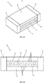
- the fuse 10 may include a bottom insulative layer 12, a first intermediate insulative layer 14, a second intermediate insulative layer 16, and a top insulative layer 18 disposed in a stacked arrangement in the aforementioned order.
- the layers 12-18 may be flatly bonded to one another, such as with epoxy or other electrically insulating adhesive or fasteners.
- the fuse 10 is shown and described herein as having only two intermediate insulative layers (the first and second intermediate insulative layers 14, 16), it is contemplated that the fuse 10 may be provided with additional intermediate insulative layers without departing from the scope of the present invention.
- the fuse 10 may be provided with a third intermediate insulative layer disposed between the bottom insulative layer 12 and the first intermediate insulative layer 14, and/or a fourth intermediate insulative layer disposed between the top insulative layer 18 and the second intermediate insulative layer 16.
- the present disclosure is not limited in this regard.
- the fuse 10 may further include a fusible element 20 disposed between the first and second intermediate insulative layers 14, 16 (e.g., sandwiched between the first and second intermediate insulative layers 14, 16) and extending between electrically conductive first and second terminals 22, 24 at opposing longitudinal ends of the layers 12-18.
- the fusible element 20 may be formed of an electrically conductive material, including, but not limited to, tin or copper, and may be formed as a wire, a ribbon, a metal link, a spiral wound wire, a film, and electrically conductive core deposited on a substrate, etc.
- the fusible element 20 may be configured to melt and separate upon the occurrence of a predetermined fault condition in the fuse 10, such as an overcurrent condition in which an amount of current exceeding a predefined maximum current (i.e., a "rating" of the fuse 10) flows through the fusible element 20.
- a predetermined fault condition in the fuse 10 such as an overcurrent condition in which an amount of current exceeding a predefined maximum current (i.e., a "rating" of the fuse 10) flows through the fusible element 20.
- a predefined maximum current i.e., a "rating" of the fuse
- the bottom insulative layer 12 and the top insulative layer 18 of the fuse 10 may be formed of any suitable dielectric material, including, but not limited to, FR-4, glass, ceramic (e.g., low temperature co-fired ceramic), etc., and may be generally non-porous.
- the first and second intermediate insulative layers 14, 16 of the fuse 10 may be formed of porous ceramic (e.g., low temperature co-fired ceramic) having pluralities of hollow pores 26 formed therein.
- the porous ceramic of the first and second intermediate insulative layers 14, 16 may be made by mixing granules or particles of one or more fugitive materials (e.g., carbon, corn starch, etc.) into the ceramic prior to firing/curing of the ceramic. During firing/curing, the particles of fugitive material may be burned away, leaving the hollow pores 26 within the ceramic.
- the present disclosure is not limited in this regard.
- the first and second intermediate insulating layers 14, 16 may have porosities greater than the porosities of the bottom and top insulative layers 12, 18 of the fuse 10. In a particular embodiment, the first and second intermediate insulating layers 14, 16 may be 25% more porous than the bottom and top insulative layers 12, 18 of the fuse 10. In another embodiment, the first and second intermediate insulating layers 14, 16 may be 50% more porous than the bottom and top insulative layers 12, 18 of the fuse 10. In another embodiment, the first and second intermediate insulating layers 14, 16 may be 75% more porous than the bottom and top insulative layers 12, 18 of the fuse 10. In another embodiment, the first and second intermediate insulating layers 14, 16 may be 100% more porous than the bottom and top insulative layers 12, 18 of the fuse 10. The present disclosure is not limited in this regard.
- the first and second intermediate insulative layers 14, 16, which are relatively weaker and more prone to breaking than the bottom insulative layer 12 and the top insulative layer 18 due to the provision of the pores 26, may fracture and may absorb the energy of the explosion (e.g., in the manner of crumple zones in an automobile), thereby preventing much of the energy from the explosion from being communicated to the bottom insulative layer 12 and the top insulative layer 18.
- the vaporized material of the melted fusible element 20 may be rapidly cleared into the pores 26 of the fractured first and second intermediate insulative layers 14, 16, thereby preventing such vaporized material from feeding and prolonging electrical arcing across separated portions of the fusible element 20.
- the risk of the fuse 10 being ruptured is mitigated by the fracturing of the first and second intermediate insulative layers 14, 16, and the breaking capacity of the fuse 10 may therefore be relatively greater than the breaking capacity of chip fuses that lack the porous first and second intermediate insulative layers 14, 16 of the fuse 10 of the present disclosure.
Landscapes
- Engineering & Computer Science (AREA)
- Manufacturing & Machinery (AREA)
- Fuses (AREA)
Abstract
Description
- This application claims the benefit of
U.S. Provisional Patent Application No. 62/906,024, filed September 25, 2019 - This disclosure relates generally to the field of circuit protection devices and relates more particularly to a chip fuse having porous inner layers adapted to absorb energy from a blown fusible element.
- Chip fuses (also commonly referred to as "solid-body" fuses) typically include a fusible element extending between two conductive endcaps and sandwiched between two or more layers of dielectric material (e.g., ceramic). When the fusible element of a chip fuse is melted or is otherwise opened during an overcurrent condition it is sometimes possible for an electrical arc to propagate between the separated portions of the fusible element. The electrical arc may rapidly heat the surrounding air and ambient particulate and may cause a small explosion within the chip fuse. In some cases, the explosion may break the dielectric layers and rupture the chip fuse, potentially causing damage to surrounding components. The likelihood of rupture is generally proportional to the severity of the overcurrent condition. The maximum current that a chip fuse can arrest without rupturing is referred to as the chip fuse's "breaking capacity." It is generally desirable to maximize the breaking capacity of a chip fuse without significantly increasing the size or form factor of the chip fuse.
- It is with respect to these and other considerations that the present improvements may be useful.
- This Summary is provided to introduce a selection of concepts in a simplified form that are further described below in the Detailed Description. This Summary is not intended to identify key features or essential features of the claimed subject matter, nor is it intended as an aid in determining the scope of the claimed subject matter.
- A high breaking capacity chip fuse in accordance with a non-limiting embodiment of the present disclosure may include a first intermediate insulative layer, a second intermediate insulative layer, and a top insulative layer disposed in a stacked arrangement in the aforementioned order, a fusible element disposed between the first and second intermediate insulative layers and extending between electrically conductive first and second terminals at opposing longitudinal ends of the bottom insulative layer, the first intermediate insulative layer, the second intermediate insulative layer, and the top insulative layer, wherein the first and second intermediate insulative layers are formed of porous ceramic.
- A method of forming a high breaking capacity chip fuse in accordance with a non-limiting embodiment of the present disclosure may include providing a bottom insulative layer, a first intermediate insulative layer, a second intermediate insulative layer, and a top insulative layer disposed in a stacked arrangement in the aforementioned order, and disposing a fusible element between the first and second intermediate insulative layers, the fusible extending between electrically conductive first and second terminals at opposing longitudinal ends of the bottom insulative layer, the first intermediate insulative layer, the second intermediate insulative layer, and the top insulative layer, wherein the first and second intermediate insulative layers are formed of porous ceramic.
- By way of example, various embodiments of the disclosed system will now be described, with reference to the accompanying drawings, wherein:
-
FIG. 1A is a perspective view illustrating a high breaking capacity chip fuse in accordance with an exemplary embodiment of the present disclosure; - FIG. IB is cross sectional view illustrating the high breaking capacity chip fuse shown in
FIG. 1A . - A high breaking capacity chip fuse in accordance with the present disclosure will now be described more fully with reference to the accompanying drawings, in which preferred embodiments of the high breaking capacity chip fuse are presented. It will be understood, however, that the high breaking capacity chip fuse described below may be embodied in many different forms and should not be construed as being limited to the embodiments set forth herein. Rather, these embodiments are provided so that this disclosure will convey certain exemplary aspects of the high breaking capacity chip fuse to those skilled in the art.
- Referring to
FIGS. 1A and 1B , a perspective view and a cross sectional side view illustrating a high breaking capacity chip fuse 10 (hereinafter "thefuse 10") in accordance with an exemplary, non-limiting embodiment of the present disclosure are shown. Thefuse 10 may include a bottominsulative layer 12, a first intermediateinsulative layer 14, a second intermediateinsulative layer 16, and a topinsulative layer 18 disposed in a stacked arrangement in the aforementioned order. The layers 12-18 may be flatly bonded to one another, such as with epoxy or other electrically insulating adhesive or fasteners. While thefuse 10 is shown and described herein as having only two intermediate insulative layers (the first and second intermediateinsulative layers 14, 16), it is contemplated that thefuse 10 may be provided with additional intermediate insulative layers without departing from the scope of the present invention. For example, thefuse 10 may be provided with a third intermediate insulative layer disposed between the bottominsulative layer 12 and the first intermediateinsulative layer 14, and/or a fourth intermediate insulative layer disposed between the topinsulative layer 18 and the second intermediateinsulative layer 16. The present disclosure is not limited in this regard. - The
fuse 10 may further include afusible element 20 disposed between the first and second intermediateinsulative layers 14, 16 (e.g., sandwiched between the first and second intermediateinsulative layers 14, 16) and extending between electrically conductive first andsecond terminals fusible element 20 may be formed of an electrically conductive material, including, but not limited to, tin or copper, and may be formed as a wire, a ribbon, a metal link, a spiral wound wire, a film, and electrically conductive core deposited on a substrate, etc. Thefusible element 20 may be configured to melt and separate upon the occurrence of a predetermined fault condition in thefuse 10, such as an overcurrent condition in which an amount of current exceeding a predefined maximum current (i.e., a "rating" of the fuse 10) flows through thefusible element 20. As will be appreciated by those of ordinary skill in the art, the size, shape, configuration, and material of thefusible element 20 may all contribute to the rating of thefuse 10. - The bottom
insulative layer 12 and the topinsulative layer 18 of thefuse 10 may be formed of any suitable dielectric material, including, but not limited to, FR-4, glass, ceramic (e.g., low temperature co-fired ceramic), etc., and may be generally non-porous. The first and second intermediateinsulative layers fuse 10 may be formed of porous ceramic (e.g., low temperature co-fired ceramic) having pluralities ofhollow pores 26 formed therein. The porous ceramic of the first and second intermediateinsulative layers hollow pores 26 within the ceramic. The present disclosure is not limited in this regard. - In various embodiments, the first and second intermediate
insulating layers insulative layers fuse 10. In a particular embodiment, the first and second intermediateinsulating layers insulative layers fuse 10. In another embodiment, the first and second intermediateinsulating layers insulative layers fuse 10. In another embodiment, the first and second intermediateinsulating layers insulative layers fuse 10. In another embodiment, the first and second intermediateinsulating layers insulative layers fuse 10. The present disclosure is not limited in this regard. - During operation of the
fuse 10, if an overcurrent condition causes thefusible element 20 to melt and produce an explosion, the first and second intermediateinsulative layers insulative layer 12 and the topinsulative layer 18 due to the provision of thepores 26, may fracture and may absorb the energy of the explosion (e.g., in the manner of crumple zones in an automobile), thereby preventing much of the energy from the explosion from being communicated to the bottominsulative layer 12 and the topinsulative layer 18. Additionally, the vaporized material of the meltedfusible element 20 may be rapidly cleared into thepores 26 of the fractured first and second intermediateinsulative layers fusible element 20. Thus, the risk of thefuse 10 being ruptured is mitigated by the fracturing of the first and second intermediateinsulative layers fuse 10 may therefore be relatively greater than the breaking capacity of chip fuses that lack the porous first and second intermediateinsulative layers fuse 10 of the present disclosure. - As used herein, an element or step recited in the singular and proceeded with the word "a" or "an" should be understood as not excluding plural elements or steps, unless such exclusion is explicitly recited. Furthermore, references to "one embodiment" of the present disclosure are not intended to be interpreted as excluding the existence of additional embodiments that also incorporate the recited features.
- While the present disclosure makes reference to certain embodiments, numerous modifications, alterations and changes to the described embodiments are possible without departing from the sphere and scope of the present disclosure, as defined in the appended claim(s). Accordingly, it is intended that the present disclosure not be limited to the described embodiments, but that it has the full scope defined by the language of the following claims, and equivalents thereof.
Claims (15)
- A high breaking capacity chip fuse comprising:a bottom insulative layer, a first intermediate insulative layer, a second intermediate insulative layer, and a top insulative layer disposed in a stacked arrangement; anda fusible element disposed between the first and second intermediate insulative layers and extending between electrically conductive first and second terminals at opposing longitudinal ends of the bottom insulative layer, the first intermediate insulative layer, the second intermediate insulative layer, and the top insulative layer;wherein the first and second intermediate insulative layers are formed of porous ceramic.
- The high breaking capacity chip fuse of claim 1, wherein the fusible element is one of a wire, a ribbon, a metal link, a spiral wound wire, a film, and electrically conductive core deposited on a substrate.
- The high breaking capacity chip fuse of claim 1 or 2, wherein the first intermediate insulative layer and the second intermediate insulative layer are more porous than the bottom insulative layer and the top insulative layer, preferably
wherein the first intermediate insulative layer and the second intermediate insulative layer are at least 25% more porous than the bottom insulative layer and the top insulative layer, more preferably
wherein the first intermediate insulative layer and the second intermediate insulative layer are at least 50% more porous than the bottom insulative layer and the top insulative layer, even more preferably wherein the first intermediate insulative layer and the second intermediate insulative layer are at least 75% more porous than the bottom insulative layer and the top insulative layer. - The high breaking capacity chip fuse of claim 3, wherein the first intermediate insulative layer and the second intermediate insulative layer are at least 100% more porous than the bottom insulative layer and the top insulative layer.
- The high breaking capacity chip fuse of any of the preceding claims, wherein the bottom insulative layer and the top insulative layer are formed of one of FR-4, glass, and ceramic.
- The high breaking capacity chip fuse of any of the preceding claims, the bottom insulative layer, the first intermediate insulative layer, the second intermediate insulative layer, and the top insulative layer are flatly bonded to one another with an electrically insulating adhesive.
- A method of forming a high breaking capacity chip fuse comprising:providing a bottom insulative layer, a first intermediate insulative layer, a second intermediate insulative layer, and a top insulative layer disposed in a stacked arrangement; anddisposing a fusible element between the first and second intermediate insulative layers, the fusible extending between electrically conductive first and second terminals at opposing longitudinal ends of the bottom insulative layer, the first intermediate insulative layer, the second intermediate insulative layer, and the top insulative layer;wherein the first and second intermediate insulative layers are formed of porous ceramic.
- The method of claim 7 , wherein the fusible element is one of a wire, a ribbon, a metal link, a spiral wound wire, a film, and electrically conductive core deposited on a substrate
- The method of claim 7 or 8, wherein the first intermediate insulative layer and the second intermediate insulative layer are more porous than the bottom insulative layer and the top insulative layer.
- The method of claim 9, wherein the first intermediate insulative layer and the second intermediate insulative layer are at least 25% more porous than the bottom insulative layer and the top insulative layer,
preferably wherein the first intermediate insulative layer and the second intermediate insulative layer are at least 50% more porous than the bottom insulative layer and the top insulative layer,
more preferably wherein the first intermediate insulative layer and the second intermediate insulative layer are at least 75% more porous than the bottom insulative layer and the top insulative layer,
even more preferably wherein the first intermediate insulative layer and the second intermediate insulative layer are at least 100% more porous than the bottom insulative layer and the top insulative layer. - The method of any of the claims 7-10, wherein the bottom insulative layer and the top insulative layer are formed of one of FR-4, glass, and ceramic.
- The method of any of the preceding claims 7-11, further comprising forming the porous ceramic by mixing particles of one or more fugitive materials into a ceramic and then firing the ceramic to burn the particles of fugitive material away, leaving hollow pores within the ceramic.
- The method of claim 12 wherein the fugitive materials include at least one of carbon and corn starch.
- The method of any of the preceding claims 7-13, further comprising flatly bonding the bottom insulative layer, the first intermediate insulative layer, the second intermediate insulative layer, and the top insulative layer to one another with an electrically insulating adhesive.
- The method of any of the preceding claims 7-14 for forming a high breaking capacity chip fuse according to any of the claims 1-6.
Applications Claiming Priority (1)
| Application Number | Priority Date | Filing Date | Title |
|---|---|---|---|
| US201962906024P | 2019-09-25 | 2019-09-25 |
Publications (2)
| Publication Number | Publication Date |
|---|---|
| EP3799103A1 true EP3799103A1 (en) | 2021-03-31 |
| EP3799103B1 EP3799103B1 (en) | 2024-04-17 |
Family
ID=72644037
Family Applications (1)
| Application Number | Title | Priority Date | Filing Date |
|---|---|---|---|
| EP20197842.6A Active EP3799103B1 (en) | 2019-09-25 | 2020-09-23 | High breaking capacity chip fuse |
Country Status (3)
| Country | Link |
|---|---|
| US (2) | US11217415B2 (en) |
| EP (1) | EP3799103B1 (en) |
| CN (1) | CN112563089B (en) |
Cited By (2)
| Publication number | Priority date | Publication date | Assignee | Title |
|---|---|---|---|---|
| WO2024121237A1 (en) * | 2022-12-06 | 2024-06-13 | Schurter Ag | Electrical fuse |
| EP4421839A1 (en) * | 2023-02-24 | 2024-08-28 | Yageo Electronics (China) Co., LTD | Explosion-proof over-current protection element and manufacturing method thereof |
Families Citing this family (1)
| Publication number | Priority date | Publication date | Assignee | Title |
|---|---|---|---|---|
| US11804351B1 (en) * | 2022-09-14 | 2023-10-31 | Littelfuse, Inc. | High breaking capacity fuse with fire-extinguishing pads |
Citations (3)
| Publication number | Priority date | Publication date | Assignee | Title |
|---|---|---|---|---|
| DE29717120U1 (en) * | 1997-09-25 | 1997-11-13 | Wickmann-Werke GmbH, 58453 Witten | Electrical fuse element |
| CN102013368B (en) * | 2010-10-08 | 2012-11-21 | Aem科技(苏州)股份有限公司 | Fuse with built-in thermal-protective coating and manufacture process thereof |
| CN106783449A (en) * | 2016-11-29 | 2017-05-31 | 苏州达方电子有限公司 | Surface-adhered fuse and its manufacture method with compacting arc structure |
Family Cites Families (23)
| Publication number | Priority date | Publication date | Assignee | Title |
|---|---|---|---|---|
| US2483577A (en) * | 1943-11-24 | 1949-10-04 | Westinghouse Electric Corp | Circuit interrupter |
| JPS5532380Y2 (en) * | 1975-11-26 | 1980-08-01 | ||
| US4272752A (en) * | 1979-07-30 | 1981-06-09 | Gould Inc. | Electric fuse including two different fillers |
| US4306213A (en) * | 1980-01-28 | 1981-12-15 | General Electric Company | Layered plastic fuse |
| CA1264791A (en) * | 1987-03-20 | 1990-01-23 | Vojislav Narancic | Fuse having a non-porous rigid ceramic arc extinguishing body and method for fabricating such a fuse |
| US5726621A (en) * | 1994-09-12 | 1998-03-10 | Cooper Industries, Inc. | Ceramic chip fuses with multiple current carrying elements and a method for making the same |
| JP2002513196A (en) * | 1998-04-24 | 2002-05-08 | ヴィックマン−ヴェルケ ゲーエムベーハー | Electric fuse |
| US6034589A (en) * | 1998-12-17 | 2000-03-07 | Aem, Inc. | Multi-layer and multi-element monolithic surface mount fuse and method of making the same |
| US7570148B2 (en) * | 2002-01-10 | 2009-08-04 | Cooper Technologies Company | Low resistance polymer matrix fuse apparatus and method |
| US7385475B2 (en) * | 2002-01-10 | 2008-06-10 | Cooper Technologies Company | Low resistance polymer matrix fuse apparatus and method |
| US7436284B2 (en) * | 2002-01-10 | 2008-10-14 | Cooper Technologies Company | Low resistance polymer matrix fuse apparatus and method |
| JP4211406B2 (en) * | 2003-01-27 | 2009-01-21 | パナソニック株式会社 | Chip-type fuse and manufacturing method thereof |
| TWI323906B (en) * | 2007-02-14 | 2010-04-21 | Besdon Technology Corp | Chip-type fuse and method of manufacturing the same |
| US8659384B2 (en) * | 2009-09-16 | 2014-02-25 | Littelfuse, Inc. | Metal film surface mount fuse |
| US9847203B2 (en) * | 2010-10-14 | 2017-12-19 | Avx Corporation | Low current fuse |
| JP5863980B2 (en) * | 2011-10-19 | 2016-02-17 | リテルヒューズ・インク | Method for manufacturing a fuse element |
| US9460882B2 (en) * | 2013-03-14 | 2016-10-04 | Littelfuse, Inc. | Laminated electrical fuse |
| US20150009007A1 (en) * | 2013-03-14 | 2015-01-08 | Littelfuse, Inc. | Laminated electrical fuse |
| US20160005561A1 (en) * | 2013-03-14 | 2016-01-07 | Littelfuse, Inc. | Laminated electrical fuse |
| US20150200067A1 (en) * | 2014-01-10 | 2015-07-16 | Littelfuse, Inc. | Ceramic chip fuse with offset fuse element |
| CN204289342U (en) * | 2014-10-27 | 2015-04-22 | 南京萨特科技发展有限公司 | Explosion-proof miniature protection component |
| US10141150B2 (en) * | 2016-02-17 | 2018-11-27 | Littelfuse, Inc. | High current one-piece fuse element and split body |
| US10538460B2 (en) * | 2018-03-15 | 2020-01-21 | General Electric Company | Ceramic slurries for additive manufacturing techniques |
-
2020
- 2020-09-17 US US17/023,601 patent/US11217415B2/en active Active
- 2020-09-23 EP EP20197842.6A patent/EP3799103B1/en active Active
- 2020-09-25 CN CN202011022259.8A patent/CN112563089B/en active Active
-
2021
- 2021-11-18 US US17/530,008 patent/US11508542B2/en active Active
Patent Citations (3)
| Publication number | Priority date | Publication date | Assignee | Title |
|---|---|---|---|---|
| DE29717120U1 (en) * | 1997-09-25 | 1997-11-13 | Wickmann-Werke GmbH, 58453 Witten | Electrical fuse element |
| CN102013368B (en) * | 2010-10-08 | 2012-11-21 | Aem科技(苏州)股份有限公司 | Fuse with built-in thermal-protective coating and manufacture process thereof |
| CN106783449A (en) * | 2016-11-29 | 2017-05-31 | 苏州达方电子有限公司 | Surface-adhered fuse and its manufacture method with compacting arc structure |
Cited By (3)
| Publication number | Priority date | Publication date | Assignee | Title |
|---|---|---|---|---|
| WO2024121237A1 (en) * | 2022-12-06 | 2024-06-13 | Schurter Ag | Electrical fuse |
| WO2024120618A1 (en) * | 2022-12-06 | 2024-06-13 | Schurter Ag | Eletrical fuse with a conducting layer arranged on a glass- like sheet and manufacturing thereof |
| EP4421839A1 (en) * | 2023-02-24 | 2024-08-28 | Yageo Electronics (China) Co., LTD | Explosion-proof over-current protection element and manufacturing method thereof |
Also Published As
| Publication number | Publication date |
|---|---|
| US20210090839A1 (en) | 2021-03-25 |
| CN112563089A (en) | 2021-03-26 |
| US11217415B2 (en) | 2022-01-04 |
| US11508542B2 (en) | 2022-11-22 |
| US20220076913A1 (en) | 2022-03-10 |
| EP3799103B1 (en) | 2024-04-17 |
| CN112563089B (en) | 2026-03-17 |
Similar Documents
| Publication | Publication Date | Title |
|---|---|---|
| US11508542B2 (en) | High breaking capacity chip fuse | |
| EP2161731A1 (en) | Protective element | |
| US6384708B1 (en) | Electrical fuse element | |
| US20100289612A1 (en) | Current protection device and the method for forming the same | |
| CN106663575B (en) | Chip fuse and its manufacturing method | |
| US12431313B2 (en) | Protection element | |
| US20240096581A1 (en) | Arc quenching fuse filler for current limiting fuses | |
| US20150200067A1 (en) | Ceramic chip fuse with offset fuse element | |
| CN106653513A (en) | Automatic control protector conforming to high-voltage and low-voltage dual-function protection and fabrication method of automatic control protector | |
| US20150009007A1 (en) | Laminated electrical fuse | |
| KR20230022131A (en) | Surface mount fuse with solder link and de-wetting substrate | |
| US20250079104A1 (en) | Protection device | |
| US20180366293A1 (en) | Electrical circuit protection device with high resistive bypass material | |
| CN204167243U (en) | Circuit protecting element | |
| EP3389077B1 (en) | Printed circuit fuse and method for use of the same | |
| US20250157774A1 (en) | Chip fuse with floating leads | |
| US11804351B1 (en) | High breaking capacity fuse with fire-extinguishing pads | |
| US11087945B1 (en) | Fuse with integrated heat shield | |
| US20140300444A1 (en) | Laminated electrical fuse | |
| CN108231506B (en) | Small fuse and manufacturing method thereof | |
| KR20240105509A (en) | Circuit module | |
| US20150102896A1 (en) | Barrier layer for electrical fuses utilizing the metcalf effect |
Legal Events
| Date | Code | Title | Description |
|---|---|---|---|
| PUAI | Public reference made under article 153(3) epc to a published international application that has entered the european phase |
Free format text: ORIGINAL CODE: 0009012 |
|
| STAA | Information on the status of an ep patent application or granted ep patent |
Free format text: STATUS: THE APPLICATION HAS BEEN PUBLISHED |
|
| AK | Designated contracting states |
Kind code of ref document: A1 Designated state(s): AL AT BE BG CH CY CZ DE DK EE ES FI FR GB GR HR HU IE IS IT LI LT LU LV MC MK MT NL NO PL PT RO RS SE SI SK SM TR |
|
| AX | Request for extension of the european patent |
Extension state: BA ME |
|
| STAA | Information on the status of an ep patent application or granted ep patent |
Free format text: STATUS: REQUEST FOR EXAMINATION WAS MADE |
|
| 17P | Request for examination filed |
Effective date: 20210930 |
|
| RBV | Designated contracting states (corrected) |
Designated state(s): AL AT BE BG CH CY CZ DE DK EE ES FI FR GB GR HR HU IE IS IT LI LT LU LV MC MK MT NL NO PL PT RO RS SE SI SK SM TR |
|
| GRAP | Despatch of communication of intention to grant a patent |
Free format text: ORIGINAL CODE: EPIDOSNIGR1 |
|
| STAA | Information on the status of an ep patent application or granted ep patent |
Free format text: STATUS: GRANT OF PATENT IS INTENDED |
|
| INTG | Intention to grant announced |
Effective date: 20231116 |
|
| GRAS | Grant fee paid |
Free format text: ORIGINAL CODE: EPIDOSNIGR3 |
|
| GRAA | (expected) grant |
Free format text: ORIGINAL CODE: 0009210 |
|
| STAA | Information on the status of an ep patent application or granted ep patent |
Free format text: STATUS: THE PATENT HAS BEEN GRANTED |
|
| AK | Designated contracting states |
Kind code of ref document: B1 Designated state(s): AL AT BE BG CH CY CZ DE DK EE ES FI FR GB GR HR HU IE IS IT LI LT LU LV MC MK MT NL NO PL PT RO RS SE SI SK SM TR |
|
| REG | Reference to a national code |
Ref country code: GB Ref legal event code: FG4D |
|
| REG | Reference to a national code |
Ref country code: CH Ref legal event code: EP |
|
| REG | Reference to a national code |
Ref country code: DE Ref legal event code: R096 Ref document number: 602020029057 Country of ref document: DE |
|
| P01 | Opt-out of the competence of the unified patent court (upc) registered |
Effective date: 20240402 |
|
| REG | Reference to a national code |
Ref country code: IE Ref legal event code: FG4D |
|
| REG | Reference to a national code |
Ref country code: LT Ref legal event code: MG9D |
|
| REG | Reference to a national code |
Ref country code: NL Ref legal event code: MP Effective date: 20240417 |
|
| REG | Reference to a national code |
Ref country code: AT Ref legal event code: MK05 Ref document number: 1678097 Country of ref document: AT Kind code of ref document: T Effective date: 20240417 |
|
| PG25 | Lapsed in a contracting state [announced via postgrant information from national office to epo] |
Ref country code: NL Free format text: LAPSE BECAUSE OF FAILURE TO SUBMIT A TRANSLATION OF THE DESCRIPTION OR TO PAY THE FEE WITHIN THE PRESCRIBED TIME-LIMIT Effective date: 20240417 |
|
| PG25 | Lapsed in a contracting state [announced via postgrant information from national office to epo] |
Ref country code: NL Free format text: LAPSE BECAUSE OF FAILURE TO SUBMIT A TRANSLATION OF THE DESCRIPTION OR TO PAY THE FEE WITHIN THE PRESCRIBED TIME-LIMIT Effective date: 20240417 |
|
| PG25 | Lapsed in a contracting state [announced via postgrant information from national office to epo] |
Ref country code: IS Free format text: LAPSE BECAUSE OF FAILURE TO SUBMIT A TRANSLATION OF THE DESCRIPTION OR TO PAY THE FEE WITHIN THE PRESCRIBED TIME-LIMIT Effective date: 20240817 |
|
| PG25 | Lapsed in a contracting state [announced via postgrant information from national office to epo] |
Ref country code: BG Free format text: LAPSE BECAUSE OF FAILURE TO SUBMIT A TRANSLATION OF THE DESCRIPTION OR TO PAY THE FEE WITHIN THE PRESCRIBED TIME-LIMIT Effective date: 20240417 |
|
| PG25 | Lapsed in a contracting state [announced via postgrant information from national office to epo] |
Ref country code: FI Free format text: LAPSE BECAUSE OF FAILURE TO SUBMIT A TRANSLATION OF THE DESCRIPTION OR TO PAY THE FEE WITHIN THE PRESCRIBED TIME-LIMIT Effective date: 20240417 Ref country code: HR Free format text: LAPSE BECAUSE OF FAILURE TO SUBMIT A TRANSLATION OF THE DESCRIPTION OR TO PAY THE FEE WITHIN THE PRESCRIBED TIME-LIMIT Effective date: 20240417 |
|
| PG25 | Lapsed in a contracting state [announced via postgrant information from national office to epo] |
Ref country code: GR Free format text: LAPSE BECAUSE OF FAILURE TO SUBMIT A TRANSLATION OF THE DESCRIPTION OR TO PAY THE FEE WITHIN THE PRESCRIBED TIME-LIMIT Effective date: 20240718 |
|
| PG25 | Lapsed in a contracting state [announced via postgrant information from national office to epo] |
Ref country code: PT Free format text: LAPSE BECAUSE OF FAILURE TO SUBMIT A TRANSLATION OF THE DESCRIPTION OR TO PAY THE FEE WITHIN THE PRESCRIBED TIME-LIMIT Effective date: 20240819 |
|
| PG25 | Lapsed in a contracting state [announced via postgrant information from national office to epo] |
Ref country code: ES Free format text: LAPSE BECAUSE OF FAILURE TO SUBMIT A TRANSLATION OF THE DESCRIPTION OR TO PAY THE FEE WITHIN THE PRESCRIBED TIME-LIMIT Effective date: 20240417 |
|
| PG25 | Lapsed in a contracting state [announced via postgrant information from national office to epo] |
Ref country code: AT Free format text: LAPSE BECAUSE OF FAILURE TO SUBMIT A TRANSLATION OF THE DESCRIPTION OR TO PAY THE FEE WITHIN THE PRESCRIBED TIME-LIMIT Effective date: 20240417 |
|
| PG25 | Lapsed in a contracting state [announced via postgrant information from national office to epo] |
Ref country code: PL Free format text: LAPSE BECAUSE OF FAILURE TO SUBMIT A TRANSLATION OF THE DESCRIPTION OR TO PAY THE FEE WITHIN THE PRESCRIBED TIME-LIMIT Effective date: 20240417 |
|
| PG25 | Lapsed in a contracting state [announced via postgrant information from national office to epo] |
Ref country code: LV Free format text: LAPSE BECAUSE OF FAILURE TO SUBMIT A TRANSLATION OF THE DESCRIPTION OR TO PAY THE FEE WITHIN THE PRESCRIBED TIME-LIMIT Effective date: 20240417 |
|
| PG25 | Lapsed in a contracting state [announced via postgrant information from national office to epo] |
Ref country code: PT Free format text: LAPSE BECAUSE OF FAILURE TO SUBMIT A TRANSLATION OF THE DESCRIPTION OR TO PAY THE FEE WITHIN THE PRESCRIBED TIME-LIMIT Effective date: 20240819 Ref country code: PL Free format text: LAPSE BECAUSE OF FAILURE TO SUBMIT A TRANSLATION OF THE DESCRIPTION OR TO PAY THE FEE WITHIN THE PRESCRIBED TIME-LIMIT Effective date: 20240417 Ref country code: NO Free format text: LAPSE BECAUSE OF FAILURE TO SUBMIT A TRANSLATION OF THE DESCRIPTION OR TO PAY THE FEE WITHIN THE PRESCRIBED TIME-LIMIT Effective date: 20240717 Ref country code: LV Free format text: LAPSE BECAUSE OF FAILURE TO SUBMIT A TRANSLATION OF THE DESCRIPTION OR TO PAY THE FEE WITHIN THE PRESCRIBED TIME-LIMIT Effective date: 20240417 Ref country code: IS Free format text: LAPSE BECAUSE OF FAILURE TO SUBMIT A TRANSLATION OF THE DESCRIPTION OR TO PAY THE FEE WITHIN THE PRESCRIBED TIME-LIMIT Effective date: 20240817 Ref country code: HR Free format text: LAPSE BECAUSE OF FAILURE TO SUBMIT A TRANSLATION OF THE DESCRIPTION OR TO PAY THE FEE WITHIN THE PRESCRIBED TIME-LIMIT Effective date: 20240417 Ref country code: GR Free format text: LAPSE BECAUSE OF FAILURE TO SUBMIT A TRANSLATION OF THE DESCRIPTION OR TO PAY THE FEE WITHIN THE PRESCRIBED TIME-LIMIT Effective date: 20240718 Ref country code: FI Free format text: LAPSE BECAUSE OF FAILURE TO SUBMIT A TRANSLATION OF THE DESCRIPTION OR TO PAY THE FEE WITHIN THE PRESCRIBED TIME-LIMIT Effective date: 20240417 Ref country code: ES Free format text: LAPSE BECAUSE OF FAILURE TO SUBMIT A TRANSLATION OF THE DESCRIPTION OR TO PAY THE FEE WITHIN THE PRESCRIBED TIME-LIMIT Effective date: 20240417 Ref country code: BG Free format text: LAPSE BECAUSE OF FAILURE TO SUBMIT A TRANSLATION OF THE DESCRIPTION OR TO PAY THE FEE WITHIN THE PRESCRIBED TIME-LIMIT Effective date: 20240417 Ref country code: AT Free format text: LAPSE BECAUSE OF FAILURE TO SUBMIT A TRANSLATION OF THE DESCRIPTION OR TO PAY THE FEE WITHIN THE PRESCRIBED TIME-LIMIT Effective date: 20240417 Ref country code: RS Free format text: LAPSE BECAUSE OF FAILURE TO SUBMIT A TRANSLATION OF THE DESCRIPTION OR TO PAY THE FEE WITHIN THE PRESCRIBED TIME-LIMIT Effective date: 20240717 |
|
| PG25 | Lapsed in a contracting state [announced via postgrant information from national office to epo] |
Ref country code: DK Free format text: LAPSE BECAUSE OF FAILURE TO SUBMIT A TRANSLATION OF THE DESCRIPTION OR TO PAY THE FEE WITHIN THE PRESCRIBED TIME-LIMIT Effective date: 20240417 |
|
| REG | Reference to a national code |
Ref country code: DE Ref legal event code: R097 Ref document number: 602020029057 Country of ref document: DE |
|
| PG25 | Lapsed in a contracting state [announced via postgrant information from national office to epo] |
Ref country code: EE Free format text: LAPSE BECAUSE OF FAILURE TO SUBMIT A TRANSLATION OF THE DESCRIPTION OR TO PAY THE FEE WITHIN THE PRESCRIBED TIME-LIMIT Effective date: 20240417 |
|
| PG25 | Lapsed in a contracting state [announced via postgrant information from national office to epo] |
Ref country code: CZ Free format text: LAPSE BECAUSE OF FAILURE TO SUBMIT A TRANSLATION OF THE DESCRIPTION OR TO PAY THE FEE WITHIN THE PRESCRIBED TIME-LIMIT Effective date: 20240417 |
|
| PG25 | Lapsed in a contracting state [announced via postgrant information from national office to epo] |
Ref country code: SK Free format text: LAPSE BECAUSE OF FAILURE TO SUBMIT A TRANSLATION OF THE DESCRIPTION OR TO PAY THE FEE WITHIN THE PRESCRIBED TIME-LIMIT Effective date: 20240417 Ref country code: RO Free format text: LAPSE BECAUSE OF FAILURE TO SUBMIT A TRANSLATION OF THE DESCRIPTION OR TO PAY THE FEE WITHIN THE PRESCRIBED TIME-LIMIT Effective date: 20240417 |
|
| PG25 | Lapsed in a contracting state [announced via postgrant information from national office to epo] |
Ref country code: SM Free format text: LAPSE BECAUSE OF FAILURE TO SUBMIT A TRANSLATION OF THE DESCRIPTION OR TO PAY THE FEE WITHIN THE PRESCRIBED TIME-LIMIT Effective date: 20240417 |
|
| PG25 | Lapsed in a contracting state [announced via postgrant information from national office to epo] |
Ref country code: SM Free format text: LAPSE BECAUSE OF FAILURE TO SUBMIT A TRANSLATION OF THE DESCRIPTION OR TO PAY THE FEE WITHIN THE PRESCRIBED TIME-LIMIT Effective date: 20240417 Ref country code: SK Free format text: LAPSE BECAUSE OF FAILURE TO SUBMIT A TRANSLATION OF THE DESCRIPTION OR TO PAY THE FEE WITHIN THE PRESCRIBED TIME-LIMIT Effective date: 20240417 Ref country code: RO Free format text: LAPSE BECAUSE OF FAILURE TO SUBMIT A TRANSLATION OF THE DESCRIPTION OR TO PAY THE FEE WITHIN THE PRESCRIBED TIME-LIMIT Effective date: 20240417 Ref country code: EE Free format text: LAPSE BECAUSE OF FAILURE TO SUBMIT A TRANSLATION OF THE DESCRIPTION OR TO PAY THE FEE WITHIN THE PRESCRIBED TIME-LIMIT Effective date: 20240417 Ref country code: DK Free format text: LAPSE BECAUSE OF FAILURE TO SUBMIT A TRANSLATION OF THE DESCRIPTION OR TO PAY THE FEE WITHIN THE PRESCRIBED TIME-LIMIT Effective date: 20240417 Ref country code: CZ Free format text: LAPSE BECAUSE OF FAILURE TO SUBMIT A TRANSLATION OF THE DESCRIPTION OR TO PAY THE FEE WITHIN THE PRESCRIBED TIME-LIMIT Effective date: 20240417 |
|
| PG25 | Lapsed in a contracting state [announced via postgrant information from national office to epo] |
Ref country code: IT Free format text: LAPSE BECAUSE OF FAILURE TO SUBMIT A TRANSLATION OF THE DESCRIPTION OR TO PAY THE FEE WITHIN THE PRESCRIBED TIME-LIMIT Effective date: 20240417 |
|
| PLBE | No opposition filed within time limit |
Free format text: ORIGINAL CODE: 0009261 |
|
| STAA | Information on the status of an ep patent application or granted ep patent |
Free format text: STATUS: NO OPPOSITION FILED WITHIN TIME LIMIT |
|
| 26N | No opposition filed |
Effective date: 20250120 |
|
| PG25 | Lapsed in a contracting state [announced via postgrant information from national office to epo] |
Ref country code: MC Free format text: LAPSE BECAUSE OF FAILURE TO SUBMIT A TRANSLATION OF THE DESCRIPTION OR TO PAY THE FEE WITHIN THE PRESCRIBED TIME-LIMIT Effective date: 20240417 Ref country code: SI Free format text: LAPSE BECAUSE OF FAILURE TO SUBMIT A TRANSLATION OF THE DESCRIPTION OR TO PAY THE FEE WITHIN THE PRESCRIBED TIME-LIMIT Effective date: 20240417 |
|
| REG | Reference to a national code |
Ref country code: CH Ref legal event code: PL |
|
| PG25 | Lapsed in a contracting state [announced via postgrant information from national office to epo] |
Ref country code: LU Free format text: LAPSE BECAUSE OF NON-PAYMENT OF DUE FEES Effective date: 20240923 |
|
| GBPC | Gb: european patent ceased through non-payment of renewal fee |
Effective date: 20240923 |
|
| PG25 | Lapsed in a contracting state [announced via postgrant information from national office to epo] |
Ref country code: GB Free format text: LAPSE BECAUSE OF NON-PAYMENT OF DUE FEES Effective date: 20240923 |
|
| REG | Reference to a national code |
Ref country code: BE Ref legal event code: MM Effective date: 20240930 |
|
| PG25 | Lapsed in a contracting state [announced via postgrant information from national office to epo] |
Ref country code: BE Free format text: LAPSE BECAUSE OF NON-PAYMENT OF DUE FEES Effective date: 20240930 |
|
| PG25 | Lapsed in a contracting state [announced via postgrant information from national office to epo] |
Ref country code: FR Free format text: LAPSE BECAUSE OF NON-PAYMENT OF DUE FEES Effective date: 20240930 |
|
| PG25 | Lapsed in a contracting state [announced via postgrant information from national office to epo] |
Ref country code: CH Free format text: LAPSE BECAUSE OF NON-PAYMENT OF DUE FEES Effective date: 20240930 |
|
| PG25 | Lapsed in a contracting state [announced via postgrant information from national office to epo] |
Ref country code: IE Free format text: LAPSE BECAUSE OF NON-PAYMENT OF DUE FEES Effective date: 20240923 |
|
| PG25 | Lapsed in a contracting state [announced via postgrant information from national office to epo] |
Ref country code: SE Free format text: LAPSE BECAUSE OF FAILURE TO SUBMIT A TRANSLATION OF THE DESCRIPTION OR TO PAY THE FEE WITHIN THE PRESCRIBED TIME-LIMIT Effective date: 20240417 |
|
| PGFP | Annual fee paid to national office [announced via postgrant information from national office to epo] |
Ref country code: DE Payment date: 20250702 Year of fee payment: 6 |
|
| PG25 | Lapsed in a contracting state [announced via postgrant information from national office to epo] |
Ref country code: CY Free format text: LAPSE BECAUSE OF FAILURE TO SUBMIT A TRANSLATION OF THE DESCRIPTION OR TO PAY THE FEE WITHIN THE PRESCRIBED TIME-LIMIT; INVALID AB INITIO Effective date: 20200923 |
|
| PG25 | Lapsed in a contracting state [announced via postgrant information from national office to epo] |
Ref country code: HU Free format text: LAPSE BECAUSE OF FAILURE TO SUBMIT A TRANSLATION OF THE DESCRIPTION OR TO PAY THE FEE WITHIN THE PRESCRIBED TIME-LIMIT; INVALID AB INITIO Effective date: 20200923 |